

Page 1

COM 830
(Computer-On-Module)
Reference Manual
P/N 5001829A Revision A
Page 2

Notice Page
NOTICE
No part of this document may be reproduced, transmitted, transcribed, stored in a retrieval system, or
translated into any language or computer language, in any form or by any means, electronic, mechanical,
magnetic, optical, chemical, manual, or otherwise, without the prior written permission of Ampro
Computers, Incorporated.
DISCLAIMER
Ampro Computers, Incorporated makes no representations or warranties with respect to the contents of this
manual or of the associated Ampro products, and specifically disclaims any implied warranties of
merchantability or fitness for any particular purpose. Ampro shall under no circumstances be liable for
incidental or consequential damages or related expenses resulting from the use of this product, even if it has
been notified of the possibility of such damages. Ampro reserves the right to revise this publication from
time to time without obligation to notify any person of such revisions. If errors are found, please contact
Ampro at the address listed below on the Notice page of this do cu ment.
TRADEMARKS
Ampro and the Ampro logo are registered trademarks, and CoreModule, EnCore, Little Board,
LittleBoard, MightyBoard, MightySystem, MiniModule, ReadyBoard, ReadyBox, ReadyPanel, and
ReadySystem are trademarks of Ampro Computers, Inc. All other marks are the property of their
respective companies.
REVISION HISTORY
Revision Reason for Change Date
A, 1 Preliminary Release Apr/07
A, A Final Release July/07
Ampro Computers, Incorporated
5215 Hellyer Avenue
San Jose, CA 95138-1007
Tel. 408 360-0200
Fax 408 360-0222
www.ampro.com
© Copyright 2007, Ampro Computers, Incorporated
Audience
This reference manual is for the person who designs computer related equipment, including but not limited
to hardware and software design and implementation of the same. Ampro Computers, Inc. assumes you are
qualified in designing and implementing your hardware designs and its related software into your prototype
computer equipment.
ii Reference Manual COM 830
Page 3

Contents
Chapter 1 About This Manual....................................................................................................1
Symbols...........................................................................................................................................1
Warning.................................................................................................................................1
Caution..................................................................................................................................1
Note.......................................................................................................................................1
Terminology.....................................................................................................................................1
Warranty ..........................................................................................................................................1
COM Express™ Concept...................... ... ... ... ....................................... ... .... ... ... ... .... ... ....................2
Certification......................................................................................................................................3
Technical Support............................................................................................................................3
Lead-Free Designs (RoHS) .................................. ....................................... ... ... ... .... ... ... ... ... .... .......3
Electrostatic Sensitive Device .........................................................................................................3
COM 830 Options Information .........................................................................................................3
Chapter 2 Specifications............................................................................................................5
Feature List......................................................................................................................................5
Usable Memory..................................... ... ... ... .... ... ... ... ....................................... ... .... ... ... .................6
Supported Operating Systems.........................................................................................................6
Mechanical Dimensions. ... .... ...................................... .... ... ... ... .... ... ... ... ... .... ... ... ..............................6
Electrostatic Sensitive Device.....................................................................................................7
Supply Voltage Standard Power......................................................................................................7
Electrical Characteristics .......................... ..................................................................................7
Power Consumption.........................................................................................................................7
Windows XP Professional SP2...................................................................................................7
Processor Information......................................................................................................................8
Environmental Specifications................................... ... .......................................... .... .......................9
Block Diagram................................................................................................................................10
Heatspreader.................................................................................................................................11
Heatspreader Dimensions .............................................................................................................12
Connector Subsystems Rows A, B, C, D.......................................................................................13
Primary Connector Rows A and B.................................................................................................13
Serial ATA™ (SATA)................................................................................................................13
USB 2.0 ................................. ... .... ... ... ... ... ....................................... ... .... ..................................13
AC'97 Digital Audio Interface/HDA ......................................... ... ... ... ... .... ... ... ... .... .....................13
Gigabit Ethernet .......................................................................................................................13
LPC Bus....................................................................................................................................13
I²C Bus 400kHz.........................................................................................................................13
PCI Express™..........................................................................................................................14
ExpressCard™ .........................................................................................................................14
Graphics Output (VGA/CRT)........ ... ... ... ... .... ... ... ... ...................................................................14
LCD...........................................................................................................................................14
TV-Out......................................................................................................................................14
Power Control................................................................................................................................14
PWR_OK .................................................................................................................................14
SUS_S5#/PS_ON#...................................................................................................................14
PWRBTN#................................................................................................................................14
Power Supply Implementation Guidelines.....................................................................................15
Power Management..................................................................................................................15
COM 830 Reference Manual iii
Page 4

Contents
Secondary Connector Rows C and D ......................................................................................15
PCI Express Graphics (PEG)...................................................................................................15
SDVO.......................................................................................................................................15
PCI Bus....................................................................................................................................15
IDE...........................................................................................................................................15
Additional Features .................................................................. ... ... .... ... ... ... ... .... ... ... ... .... ..............15
Watchdog.................................................................................................................................15
Onboard Microcontroller...........................................................................................................16
Embedded BIOS .................................................... ... ... .... ... ... ... .... ... ... .....................................16
Simplified Overview of BIOS Setup Data Backup....................................................................17
Security Features.......................................................................................................................... 18
Suspend to Ram...................... .... ... ... ... .... ...................................... .... ... ... ... ... .... ... ........................18
Ampro Tech Notes ...................... ... ... ... .... ... ... ... ... ....................................... ... .... ... ... .....................18
Comparison of I/O APIC to 8259 PIC Interrupt mode ...................................................................18
Intel® Matrix Storage Technology ........................... .....................................................................18
AHCI......................................................................................................................................... 18
RAID.........................................................................................................................................18
Native vs. Compatible IDE mode ..................................................................................................19
Compatible Mode................................... ... ... ... .... ... ... ... .... ... ... ... .... ... ........................................ 19
Native Mode ............................................................................................................................19
Intel® Processor Features.............................. ... ... .... ... ... ... .... ... ... ... .... ... ... ... ... .... ... ... ... .... ... ... ........ 19
Thermal Monitor and Catastrophic Thermal Protection ...........................................................19
Processor Performance Control...............................................................................................20
Intel 64 .....................................................................................................................................20
Intel® Virtualization Technology...............................................................................................21
Thermal Management...................................................................................................................21
Passive Cooling ..................................................................................................................21
Active Cooling............................ .... ... ....................................... ... ... ... ... ...............................22
Critical Trip Point.................................................................................................................22
ACPI Suspend Modes and Resume Events..................................................................................22
USB 2.0 EHCI Host Controller Support......................................................................................... 24
Routing Diagram:..................................................................................................................... 24
Chapter 3 Signals and Pinout Tables..................................................................................... 25
A-B Connector Signal Descriptions...............................................................................................26
A-B Connector Pinout....................................................................................................................36
C-D Connector Signal Descriptions...............................................................................................38
C-D Connector Pinout...................................................................................................................43
Boot Strap Signals....................... ... ... ... .... ...................................... .... ... ... ... ... .... ... ... ... .... ..............45
System Resources ............................................ ... .... ... ... ... .... ... ... ....................................... ........... 46
System Memory Map... ... ... .... ...................................... .... ... ... ... .... ... ... .....................................46
I/O Address Assignment................................................................................................................46
LPC Bus...................................................................................................................................47
Interrupt Request (IRQ) Lines .......................................................................................................48
PCI Configuration Space Map.......................................................................................................49
PCI Interrupt Routing Map.............................................................................................................51
PCI Bus Masters ...........................................................................................................................52
I²C Bus .......................................................................................................................................... 52
SM Bus.......................................................................................................................................... 52
iv Reference Manual COM 830
Page 5

Contents
Chapter 4 BIOS Setup Description..........................................................................................53
Entering the BIOS Setup Program.................................................................................................53
Boot Selection Popup............... .... ... ... ... ... .... ... ... ... ....................................... ... .... ... ... ... ... .... .....53
Manufacturer Default Settings ..................................................................................................53
Setup Menu and Navigation...........................................................................................................53
Main Setup Screen ........................................................................................................................54
Advanced Setup.............................................................................................................................55
ACPI Configuration Submenu...................................................................................................56
Win XP Watchdog ACPI Event restart configuration .....................................................................57
PCI Configuration Submenu.....................................................................................................57
PCI IRQ Resource Exclusion Submenu..............................................................................58
PCI Interrupt Routing Submenu ..........................................................................................58
Graphics Configuration Submenu.............................................................................................58
CPU Configuration Submenu ................................ ...................................................................61
Chipset Configuration Submenu...............................................................................................63
I/O Interface Configuration Submenu.......................................................................................64
SIO Winbond W83627 Configuration ..................................................................................65
Clock Configuration ...................................... ... ... ... .... ... ... ....................................... ... ... ... .........66
IDE Configuration Submenu.....................................................................................................66
Primary/Secondary IDE Master/Slave Submenu............... ... ... ... ... .... ... ... ... .........................68
USB Configuration Submenu..................................................................... ... ............................70
USB Mass Storage Device Configuration Submenu ...........................................................71
Keyboard/Mouse Configuration Submenu................................................................................71
Remote Access Configuration Submenu..................................................................................72
Hardware Monitoring Submenu................................................................................................73
Watchdog Configuration Submenu...........................................................................................74
Boot Setup.................. ... ... .... ...................................... .... ... ... ....................................... ..................75
Boot Device Priority.................. .... ... ... ... ... .... ............................................................................76
Boot Settings Configuration............................................. ....................................... ... ... ... .... .....77
Security Setup................................................................................................................................78
Security Settings.......................................................................................................................79
Hard Disk Security....................................................................................................................79
Hard Disk Security User Password .....................................................................................80
Hard Disk Security User Password .....................................................................................80
Power Setup ..................................................................................................................................80
Exit Menu..................................................................................................................................81
Additional BIOS Features ........................................ ... .... .......................................... ... ..................81
Updating the BIOS...... ....................................... ... ... ... .... ... ... ... ....................................... ... ............81
BIOS Recovery..............................................................................................................................81
BIOS Recovery via Storage Devices........................................................................................81
BIOS Recovery via Serial Port..................................................................................................81
Serial Port and Console Redirection..............................................................................................82
BIOS Security Features.................................................................................................................82
Hard Disk Security Features..........................................................................................................82
Industry Specifications....................................... ... ... ... .... ... ... ....................................... ... ... ............83
Appendix A Technical Support...................................................................................................85
COM 830 Reference Manual v
Page 6

Contents
List of Tables
Table 1-1. Definitions of Terms ......................... ... .......................................... ... .......................1
Table 1-2. COM Express Pinout Types................................... .... ... .......................................... 2
Table 1-3. COM 830 Configuration Matrix................................................................................3
Table 2-1. Feature Summary................... ... ... .... ... ... ... .... .......................................... ... .............5
Table 2-2. Dual Connector Pinout Limitations.......................................................................... 7
Table 2-3. COM 830 Intel® Core™ Duo U2500 1.2G Hz 2MB L2 cache.................................. 8
Table 2-4. COM 830 Intel® Celeron M 423 1.07GHz 1MB L2 cache.......................................9
Table 3-1. Signal Tables Terminology Descriptions...............................................................25
Table 3-2. AC'97/Intel® High Definition Audio Link Signals Descriptions...............................26
Table 3-3. Gigabit Ethernet Signal Descriptions.....................................................................27
Table 3-4. Serial ATA Signal Descriptions ............................................................................ 27
Table 3-5. PCI Express Signal Descriptions [general purpose] .............................................28
Table 3-6. ExpressCard Support Pins Descriptions ...............................................................29
Table 3-7. LPC Signal Descriptions........................................................................................29
Table 3-8. USB Signal Descriptions ......................................................................................30
Table 3-9. CRT Signal Descriptions ......................................................................................31
Table 3-10. LVDS Signal Descriptions...................... ... .... ... ... ... .... ... ... ... ... .... ... ... ... .... ... ... ... .....32
Table 3-11. TV-Out Signal Descriptions ..................................................................................32
Table 3-12. Miscellaneous Signal Descriptions........................................................................33
Table 3-13. General Purpose I/O Signal Descriptions .............................................................34
Table 3-14. Power and System Management Signal Descriptions ......................................... 34
Table 3-15. Power and GND Signal Descriptions ....................................................................35
Table 3-16. Connector A-B Pinout.......................................... .......................................... ... ... .. 36
Table 3-17. PCI Signal Descriptions ........................................................................................38
Table 3-18. IDE Signal Descriptions ........................................................................................39
Table 3-19. PCI Express Signal Descriptions (x16 Graphics)..................................................40
Table 3-20. SDVO Signal Descriptions .............................. ... ... .... ... ... ... ... .... ... ... ... .... ... ... ... .....41
Table 3-21. Module Type Definition Signal Description............................................................42
Table 3-22. Power and GND Signal Descriptions ....................................................................42
Table 3-23. Connector C-D Pinout .................................................................. ... ... .... ..............43
Table 3-24. Boot Strap Signal Descriptions ............................................................................. 45
Table 3-25. Memory Map .......................................... ... .... ... ... ... .... ... ...................................... .. 46
Table 3-26. I/O Address Assignment...................................... ... .... ......................................... .. 47
Table 3-27. IRQ Lines in PIC mode........................................ ... .... ... ... ... ... .... ... ... ... ..................48
Table 3-28. IRQ Lines in APIC mode .............................................................. ... ... .... ... ... ... ... .. 48
Table 3-29. PCI Configuration Space Map ..............................................................................49
Table 3-30. PCI Interrupt Routing Map................................... ... ....................................... ... ... .. 51
Table 3-31. PCI Interrupt Routing Map (continued).................................................................. 52
Table 3-32. LAN ........................................... ... .... ... ... ... ....................................... ... .... ... ... ........ 52
Table A-1. Technical Support Contact Information................................................................. 85
vi Reference Manual COM 830
Page 7

Chapter 1 About This Manual
This manual provides information about the components, features, connectors and BIOS Setup menus
available on the COM 830.
Symbols
The following symbols are used in this manual:
Warning
Warnings indicate conditions that, if not observed, can cause personal injury.
Caution
Cautions warn the user about how to prevent damage to hardware or loss of data.
Note
Notes call attention to important information that should be observed.
Terminology
Table 1-1. Definitions of Terms
Term Description
GB Gigabyte (1,073,741,824 bytes)
GHz Gigahertz (one billion hertz)
kB Kilobyte (1024 bytes)
MB Megabyte (1,048,576 bytes)
Mb Megabit (1,048,576 bits)
kHz Kilohertz (one thousand hertz)
MHz Megahertz (one million hertz)
TDP Thermal Design Power
PCIe P C I E xpress
SATA Serial ATA
PATA Parallel ATA
T.O.M. Top of memory = max. DRAM installed
HDA High Definition Audio
I/F Interface
N.C. Not connected
N.A. Not available
TBD To be determined
Warranty
Ampro makes no representation, warranty or guaranty, express or implied regarding the products except its
standard form of limited warranty ("Limited Warranty"). Ampro may in its sole discretion modify its
Limited Warranty at any time and from time to time.
COM 830 Reference Manual 1
Page 8

Chapter 1 About This Manual
Beginning on the date of shipment to its direct customer and continuing for the publi shed warranty period,
Ampro represents that the products are new and warrants that each product failing to function properly under
normal use, due to a defect in materials or workmanship or due to non conformance to the agreed upon
specifications, will be repaired or exchanged, at Ampro's option and expense.
Customer will obtain a Return Material Authorization ("RMA") number from Ampro prior to returning the
non conforming product freight prepaid. Ampro will pay for transporting the repaired or exchanged product
to the customer.
Repaired, replaced or exchanged product will be warranted for the repair warranty period in effect as of the
date the repaired, exchanged or replaced product is shipped by Ampro, or the rem ainder of the original
warranty, whichever is longer. This Limited Warranty extends to Ampro's direct customer only and is not
assignable or transferable.
Except as set forth in writing in the Limited Warranty, Ampro makes no performance representations,
warranties, or guarantees, either express or implied, oral or written, with respect to the products, including
without limitation any implied warranty (a) of merchantability, (b) of fitness for a particular purpose, or (c)
arising from course of performance, course of dealing, or usage of trade.
Ampro shall in no event be liable to the end user for collateral or consequential damages of any kind. Ampro
shall not otherwise be liable for loss, damage or expense directly or indirectly arising from the use of the
product or from any other cause. The sole and exclusive remedy against Ampro, whether a claim sound in
contract, warranty, tort or any other legal theory, shall be repair or replacement of the product only
COM Express™ Concept
COM Express™ is an open industry standard defined specifically for COMs (computer on modules). Its
creation provides the ability to make a smooth transition from legacy parallel interfaces to the newest
technologies based on serial buses available today. COM Express™ modules are available in the following
form factors:
• Compact 95mm x 95mm (not specified by PICMG
®
)
• Basic 25mm x 95mm
• Extended 55mm x 110mm
The COM Express™ specification 1.0 defines five different pinout types.
Table 1-2. COM Express Pinout Types
Types Connector Rows PCI Express Lanes PCI IDE Channels LAN ports
Type 1 A-B Up to 6 1
Type 2 A-B C-D Up to 22 32 bit 1 1
Type 3 A-B C-D Up to 22 32 bit 3
Type 4 A-B C-D Up to 32 1 1
Type 5 A-B C-D Up to 32 3
Ampro modules utilize the Type 2 pinout definition. They are equipped with two high performance
connectors that ensure stable data throughput.
The COM (computer on module) integrates all the core components and is mounted onto an application
specific carrier board. COM modules are a legacy-free design (no Super I/O, PS/2 keyboard and mouse) and
provide most of the functional requirements for any application. These functions include, but are not limited
to, a rich complement of contemporary high bandwidth serial interfaces such as PCI Express, Serial ATA,
USB 2.0, and Gigabit Ethernet. The Type 2 pinout provides the ability to offer 32-bit PCI, Parallel ATA, and
LPC options thereby expanding the range of potential peripherals. The robust thermal and mechanical
concept, combined with extended power management capabilities, is perfectly suited for all applications.
2 Reference Manual COM 830
Page 9
Chapter 1 About This Manual
Carrier board designers can utilize as little or as many of the I/O interfaces as necessary. The carrier board
can therefore provide all the interface connectors required to attach the system to the application specific
peripherals. This versatility allows the designer to create a dense and optimized package, which results in a
more reliable product while simplifying system integration. Most importantly, COM Express™ modules are
scalable, which means once an application has been created there is the ability to diversify the product range
through the use of different performance class or form factor size modules. Simply unplug one module and
replace it with another, no redesign is necessary.
Certification
Ampro is certified to DIN EN ISO 9001:2000 standard.
Technical Support
Ampro technicians and engineers are committed to providing the best possible technical support for our
customers so that our products can be easily used and implemented. We request that you first visit our
website at www.ampro.com for the latest documentation, utilities and drivers, which have been made
available to assist you. If you still require assistance after visiting our website then contact our technical
support department by email at www.ampro.com.com/Support/.
Lead-Free Designs (RoHS)
As of July 2006 all electronic products are required to be environmentally friendly. In the future, many of the
currently available embedded computer modules will not be offered as lead-free variants. For this reason all
Ampro designs are created from lead-free components and are completely RoHS compliant. This makes
Ampro products ideal lead-free substitutes for new and exi st ing de signs.
Electrostatic Sensitive Device
All Ampro products are electrostatic sensitive devices and are packaged accordingly. Do not open or handle
an Ampro product except at an electrostatic-free workstation. Additionally, do not ship or store Ampro
products near strong electrostatic, electromagnetic, magnetic, or radioactive fields unless the device is
contained within its original manufacturer's packaging. Be aware that failure to comply with these
guidelines will void the Ampro Limited Warranty.
COM 830 Options Information
The COM 830 is currently available in two different variants. This manual describes all of these options.
Below you will find an order table showing the different configurations that are currently offered by Ampro.
Check the table for the Part no./Order no. that applies to your product. This will tell you which options
described in this manual are available on your particular module.
Table 1-3. COM 830 Configuration Matrix
Part-No. COM 830-R-30 COM 830-R-10
CPU
L2 Cache 2 MByte 1 MByte
FSB 533MHz 533MHz
CPU TDP 9 W 5.5 W
Intel® Core™ Duo U2500 ULV
1.2GHz (Ultra Low Voltage)
Intel® Celeron M 423 1.07GHz ULV
(Ultra Low Voltage)
COM 830 Reference Manual 3
Page 10

Chapter 1 About This Manual
4 Reference Manual COM 830
Page 11
Chapter 2 Specifications
Feature List
Table 2-1. Feature Summary
Form Factor
Processor
Memory
Chipset
Audio
Ethernet
Graphics
Options
Based on COM Express™ standard pinout Type 2 (Basic size 95 x 125mm)
Intel® Core™ Duo U2500 ULV 1.2GHz, with 2-MByte L2 cache ULV (Ultra
Low Voltage)
Intel® Celeron M 423 UL V 1.07GHz, with 1-MByte L2 cache (Ultra Low Voltage)
2 sockets: SO-DIMM DDR2 667 up to 4-GByte physical memory. Sockets located
top and bottom side of module.
Graphics and Memory Controller Hub (GMHC) Intel
®
I/O Controller Hub 82801GHM (ICH7M-DH)
Intel
AC‘97 Rev.2.2 compatible, HDA (High Definition Audio)/digital audio interface
with support for multiple codecs
Gigabit Ethernet, Marvell 88E8056 (uses one x1 PCI Express Lane)
Intel® Graphics Media Accelerator 950 with max.224MByte Dynamic Video
Memory Technology (DVMT 3.0) as well as Dual independent display support.
CRT Interface
400 MHz RAMDAC
Resolutions up to 2048x1536 @ 70Hz
(QXGA) including 1920x1080 @ 85Hz
(HDTV)
Flatpanel Interface (integrated)
2x112MHz LVDS Transmitter
Supports all 1x18, 2x18, 1x24, 2x24 Bit TFT
configurations (current chipset revisions
support 24Bit modes although not officially
®
stated by Intel
Supports both conventional (FPDI) and non-
conventional (LDI) color mappings
Automatic Panel Detection via EPI
(Embedded Panel Interface based on VESA
EDID™ 1.3)
)
®
82945GM
Motion Video Support
Up- and Downscaling
High definition content decode
H/W motion compensation
Subpicture support
Dynamic bob and weave
AUX Output
2 x Intel compliant SDVO ports
(serial DVO) 200MPixel/sec each
(shared with PEG x16 pins)
Supports external DVI, TV and
LVDS transmitter
TV Out: Integrated TV encoder
Supports component + s-video
Resolutions 640x480 up to 1920x1200
(UXGA)
Peripheral
Interfaces
COM 830 Reference Manual 5
2x Serial ATA® supports RAID 0/1
5x x1 PCI Express® Lanes
PCI Express Graphics x16 (shared
with SDVO)
8x USB 2.0 (EHCI)
PCI Bus Rev. 2.3
1x EIDE (UDMA-66/100)
LPC Bus
I2C Bus, Fast Mode (400 kHz)
multimaster
Page 12
Chapter 2 Specifications
Table 2-1. Feature Summary (Continued)
®
BIOS
Power
Management
NOTE Some of the features mentioned in the above Feature Summary are optional.
Based on AMIBIOS8
ACPI 2.0 compliant with battery support. Also supports Suspend to RAM (S3).
Check the article number of your module and compare it to the option
information listed in Tables 2-3 and 2-4 on page 9 of this manual to determine
what options are available on your particular module.
-1MByte Flash BIOS with Embedded BIOS features.
Usable Memory
Although the Intel® 82945GM Graphics and Memory Controller Hub (GMHC) supports up to 4GB of
physical memory, not all of the available memory is usable for applications. This is due to the fact that some
of the physical memory will always be allocated to the following:
Legacy MMIO (Memory Mapped I/O)
Chipset MMIO
PCI Enumeration Area
In order to provide full support for the above mentioned areas, usable memory is limited to 3GB on the
COM 830 when a maximum of 4GB physical memory is installed.
Supported Operating Systems
The COM 830 supports the following operating systems.
®
Microsoft
Linux
Windows ®XP Embedded
Mechanical Dimensions
95.0 mm x 125.0 mm (3.74" x 4.92")
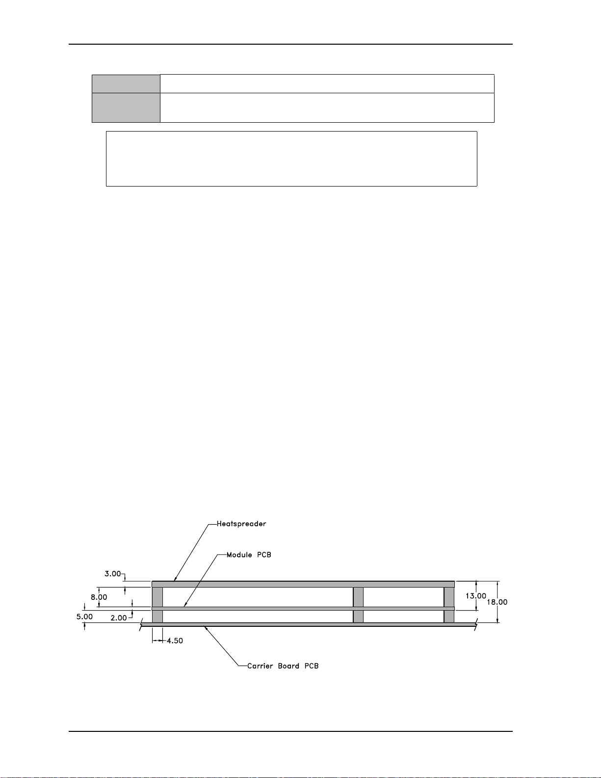
Height approx. 18 or 21mm (including heatspreader) depending on the carrier board connector that is used.
If the 5mm (height) carrier board connector is used then approximate overall height is 18mm. If the 8mm
(height) carrier board connector is used then approximate overall height is 21mm.
6 Reference Manual COM 830
Page 13

Chapter 2 Specifications
Electrostatic Sensitive Device
All COM 830 variants are electrostatic sensitive devices. Do not handle the COM 830, or processor, except
at an electrostatic-free workstation. Failure to do so may cause damage to the module and/or processor and
void the manufacturer’s warranty.
Supply Voltage Standard Power
12V DC ± 5%
Electrical Characteristics
Power supply pins on the module's connectors limit the amount of input power. The following table provides
an overview of the limitations for pinout Type 2 (dual connector, 440 pins).
Table 2-2. Dual Connector Pinout Limitations
Power
Rail
VCC_
12V
VCC_
5VSBY
VCC_
RTC
Module
Pin
Current
Capability
(Amps)
16.5 12 11.4-
2 5 4.75-
0.5 3 2.0-3.3 +/- 20
Nominal
Input
(Volts)
Input
Range
(Volts)
12.6
5.25
Derated
Input
(Volt)
11.4 +/- 100 188 85% 160
4.75 +/- 50 9
Max.
Input
Ripple
(mV)
Max. Module
Input Power
(w. derated
input)(Watts)
Assumed
Conversion
Efficiency
Max. Load
Power
(Watts)
Power Consumption
The power consumption values listed in this document were measured under a controlled environment. The
hardware used includes a COM 830 module, Ampro baseboard, CRT monitor, SATA drive, and USB
keyboard. The complete testing environment was powered by a Direct Current (DC) power supply that is set
to output 12V. The current consumption value displayed by the DC pow er supply's readout is the value that
is recorded as the power consumption measurement. All recorded values are approximate.
The power consumption of the Ampro baseboard (without module attached) was first measured and the
resulting value was later subtracted from the overall power consumption value measured when the module
and all peripherals were connected.
The SATA drive was powered externally by an ATX power supply so that it does not influence the power
consumption value that is measured for the module. The USB keyboard was detached once the module was
configured within the OS.
Each module was measured while running Windows XP Professional with SP2 (service pack 2) and the
“Power Scheme” was set to “Portable/Laptop”. This setting ensures that Core 2 Duo and Core Duo
processors run in LFM (lowest frequency mode) with minimal co re vol tage during desktop idle. Celeron M
processors do not support this feature and therefore always run at the same core voltage even during desktop
idle. Each module was tested while using a swissbit
different sizes of RAM, as well as two memory modules, will cause slight variances in the measured results.
Power consumption values were recorded during the following stages:
® DDR2 PC2-4200-444 512MB memory module. Using
Windows XP Professional SP2
Desktop Idle (1000MHz for 667MHz FSB or 800MHz for 533MHz FSB modules)
100% CPU workload (see note below)
COM 830 Reference Manual 7
Page 14
Chapter 2 Specifications
Windows XP Professional Standby Mode (requires setup node “Suspend Mode” in the BIOS to be
configured to S1 POS [Power On Suspend])
Suspend to RAM (requires setup node “Suspend Mode” in BIOS to be configured to S3 STR [suspend to
RAM])
NOTE The PassMark, Burn-In Test-Suite was used to stress the CPU to 100% workload.
Processor Information
In the following power tables there is some additional information about the processors. Intel® offers
processors that are considered to be low power consuming. These processors can be identified by their
voltage status. Intel uses the following terms to describe these processors. If none of these terms are used
then the processor is not considered to be low power consuming.
LV=Low voltage
ULV=Ultra low voltage
When applicable, the above mentioned terms will be added to the power tables to describe the processor. For
example:
®
Intel
Core™ Duo L2400 1.66GHz 2MB L2 cache LV
®
Intel
also describes the type of manufacturing process used for each processor. The following term is
used:
nm=nanometer
The manufacturing process description is included in the power tables as well. See example below. For
information about the manufacturing process, visit Intel's website.
®
Intel
Core™ Duo L2400 1.66GHz 2MB L2 cache LV 65nm
Table 2-3. COM 830 Intel® Core™ Duo U2500 1.2GHz 2MB L2 cache
COM 830-R-30
Intel® Core™ Duo U2500 1.2GHz 2MB L2 cache
ULV 65nm
Layout Rev.B945LX0 /BIOS Rev. B945R007
Memory Size
Operating System
Power State Desktop Idle 100%
Power consumption (measured
512MB
Windows XP Professional SP2
Standby (S1) Suspend to
workload
Ram (S3)
0.99A/11.88 W 2.07A/24.84 W 1.62A/19.49W 0.81A/9.78W
in Amperes/Watts)
8 Reference Manual COM 830
Page 15
Chapter 2 Specifications
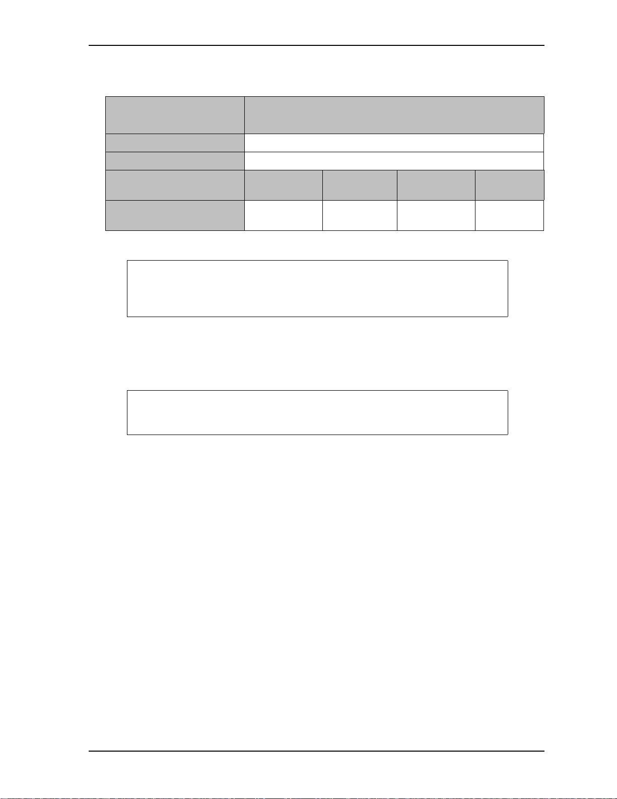
Table 2-4. COM 830 Intel® Celeron M 423 1.07GHz 1MB L2 cache
COM 830-R-10
Memory Size
Operating System
Power State Desktop Idle 100%
Power consumption
(measured in Amperes/Watts)
NOTE All recorded power consumption values are approximate and only valid for the
controlled environment described earlier. Power consumption results will vary
depending on the workload of other components such as graphics engine,
memory, etc.
Intel® Celeron M 423 1.06GHz 1MB L2 cache
ULV 65nm
512MB
Windows XP Professional SP2
1.26A/15.10W 1.90A/22.82W 1.60A/19.23W 0.82A/9.86W
Environmental Specifications
Temperature Operation: 0° to 60°C Storage: -20° to +80°C
Humidity Operation: 10% to 90% Storage: 5% to 95%
workload
Standby (S1) Suspend to
Ram (S3)
CAUTION The above operating temperatures must be strictly adhered to at all times.
When using a heatspreader the maximum operating temperature refers to
any measurable spot on the heatspreader's surface.
Ampro strongly recommends that you use the appropriate module heatspreader as a thermal interface
between the module and your application’s cooling solution.
If for some reason it is not possible to use the appropriate module heatspreader, then it is the responsibility
of the operator to ensure that all components found on the module operate within the component
manufacturer’s specified temperature range.
COM 830 Reference Manual 9
Page 16
Chapter 2 Specifications
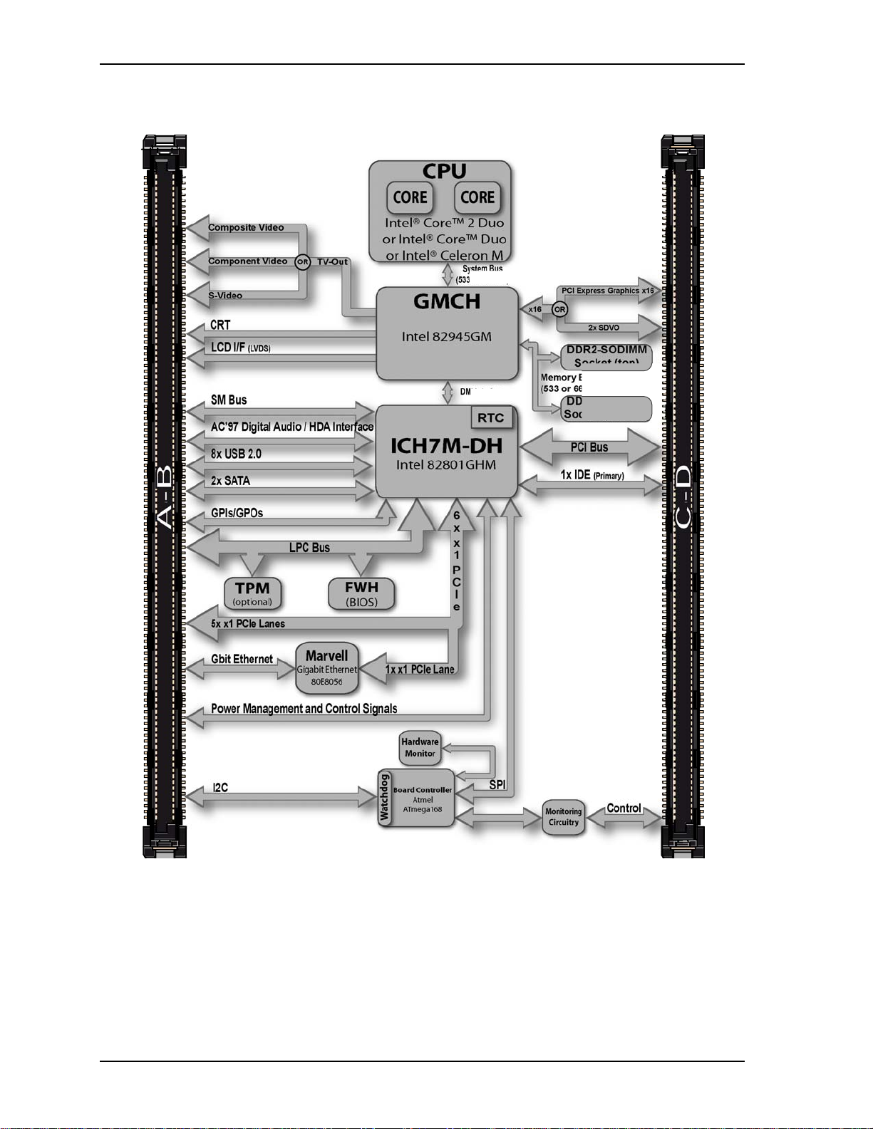
Block Diagram
Composite Video
Component Video
S-Video
OR
CRT
LCD I/F
(LVDS)
SM Bus
AC’97 Digital Audio / HDA Interface
8x USB 2.0
2x SATA
GPIs/GPOs
A-B
LPC Bus
5x x1 PCIe Lanes
Gbit Ethernet
TV-Out
System Bus
(533 or 667MHz)
GMCH
Intel 82945GM
DMI Interface
[
[
3&,H
1x x1 PCIe Lane
PCI Express Graphics x16
x16
OR
DDR2-SODIMM
Socket (top)
Memory Bus
(533 or 667MHz)
DDR2-SODIMM
Socket (bottom)
PCI Bus
1x IDE
2x SDVO
(Primary)
Power Management and Control Signals
I2C
SPI
Fan
Control
10 Reference Manual COM 830
Page 17

Chapter 2 Specifications
Heatspreader
An important factor for each system integration is the thermal design. The heatspreader acts as a thermal
coupling device to the module. It is a 3mm thick aluminum plate.
The heatspreader is thermally coupled to the CPU via a thermal gap filler and on some modules it may also
be thermally coupled to other heat generating components with the use of additional thermal gap fillers.
Although the heatspreader is the thermal interface where most of the heat generated by the module is
dissipated, it is not to be considered as a heatsink. It has been designed to be used as a thermal interface
between the module and the application specific thermal solution. The application specific thermal solution
may use heatsinks with fans, and/or heat pipes, which can be attached to the heatspreader. Some thermal
solutions may also require that the heatspreader is attached directly to the systems chassis therefore using the
whole chassis as a heat dissipater.
CAUTION Att e nti on must be given to the mounting solution used to mount the heatspreader
and module into the system chassis. Do not use a threaded heatspreader together
with threaded carrier board standoffs. The combination of the two threads may be
staggered, which could lead to stripping or cross-threading of the threads in either
the standoffs of the heatspreader or carrier board.
COM 830 Reference Manual 11
Page 18
Chapter 2 Specifications
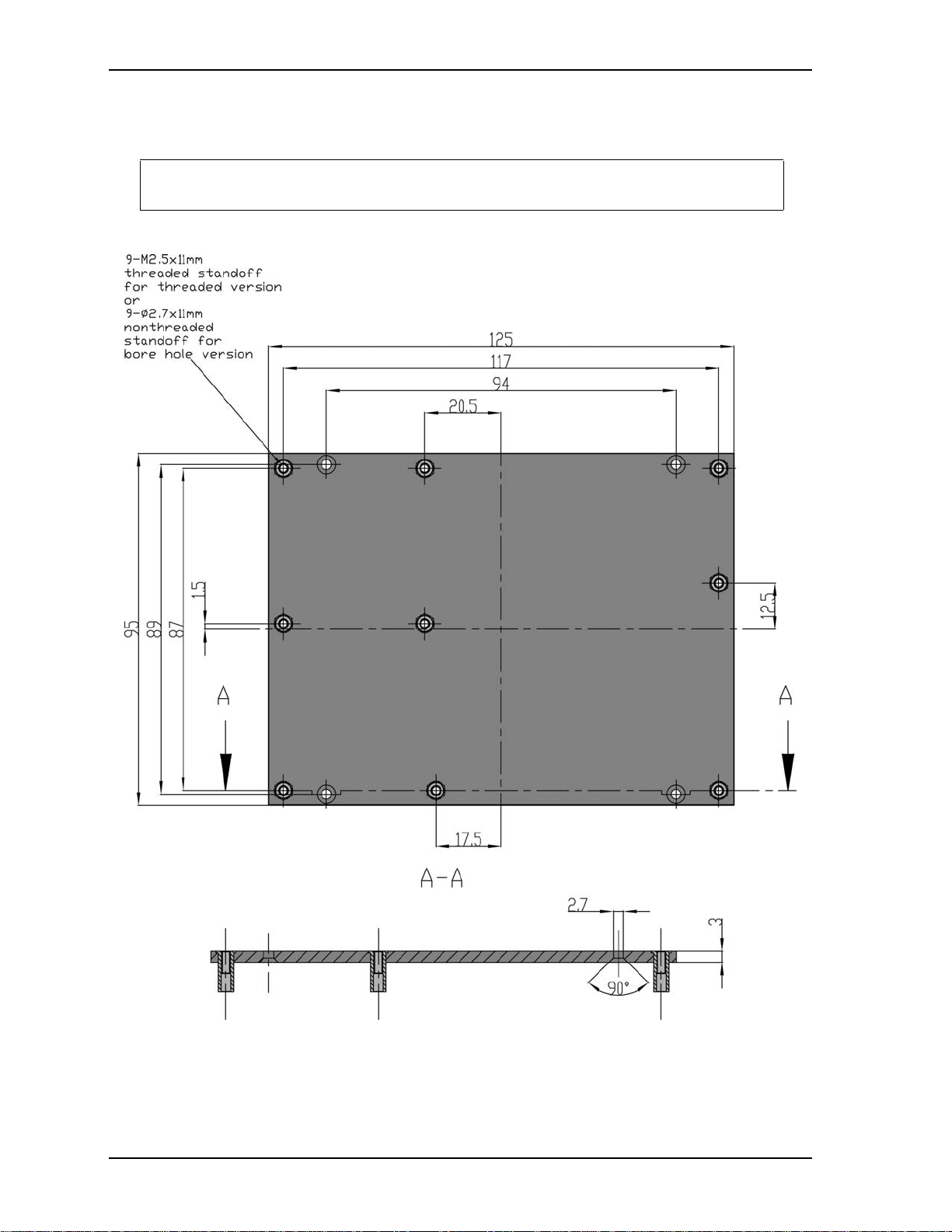
Heatspreader Dimensions
Heatspreader is available for all variants of COM 830.
NOTE All measurements are in millimeters. Torque specification for heatspreader screws is 0.5
Nm.
12 Reference Manual COM 830
Page 19

Chapter 2 Specifications
Connector Subsystems Rows A, B, C, D
The COM 830 is connected to the carrier board via two 220-pin connectors (COM Express Type 2 pinout)
for a total of 440 pins connectivity. These connectors are broken down into four rows. The primary
connector consists of rows A and B while the secondary connector consists of rows C and D.
In this view the connectors are seen “through” the module.
Primary Connector Rows A and B
The following subsystems can be found on the primary connector rows A and B.
Serial ATA™ (SATA)
Two Serial ATA150 connections are provided via the Intel® 82801GHM (ICH7M-DH). SATA is an
enhancement of the parallel A TA therefore offering higher performance. As a result of this enhancement the
traditional restrictions of parallel ATA are overcome with respect to speed and EMI. SATA starts with a
transfer rate of 150 Mbytes/s and can be expanded up to 600 Mbytes/s in order to accommodate future
developments. SATA is completely protocol and software compatible to parallel ATA.
USB 2.0
The COM 830 offers 4 UHCI USB host controllers and one EHCI USB host controller provided by the
®
Intel
82801GHM (ICH7M-DH). These controllers comply with USB standard 1.1 and 2.0 and offer a total
of 8 USB ports via connector rows A and B.
NOTE The USB controller is a PCI bus device. The BIOS allocates the necessary
system resources when configuring the PCI devices.
AC'97 Digital Audio Interface/HDA
The COM 830 provides an interface that supports the connection of AC'97 digital audio codecs as well as
HDA audio codecs.
Gigabit Ethernet
The COM 830 is equipped with a Marvell 88E8056 Gigabit Ethernet Controller. This controller is
implemented through the use of the sixth x1 PCI Express lane. The Ethernet interface consists of 4 pairs of
low voltage differential pair signals designated from GBE0_MD0 (+ and -) to GBE0_MD3 (+ and -) plus
control signals for link activity indicators. These signals can be used to connect to a 10/100/1000 BaseT
RJ45 connector with integrated or external isolation magnetics on the carrier board.
LPC Bus
COM 830 offers the LPC (Low Pin Count) bus through the use of the Intel® 82801GHM (ICH7M-DH).
There are already many devices available for this Intel defined bus. The LPC bus corresponds approximately
to a serialized ISA bus yet with a significantly reduced number of signals. Due to the software compatibility
to the ISA bus, I/O extensions such as additional serial ports can be easily implemented on an application
specific baseboard using this bus.
I²C Bus 400kHz
The I²C bus is implemented through the use of AT MEL ATmega168 microcontroller. It provides a Fast
Mode (400kHz max.) multi-master I²C Bus that has maximum I²C bandwidth.
COM 830 Reference Manual 13
Page 20

Chapter 2 Specifications
PCI Express™
The COM 830 offers 6x x1 PCI Express lanes via the Intel 82801GHM (ICH7M-DH), which can be
configured to support PCI Express edge cards or ExpressCards. One of the six x1 PCI Express lane is
utilized by the onboard Ethernet controller therefore there are only 5x x1 PCI Express lanes available on the
A,B connector row. The PCI Express interface is based on the PCI Express Specification 1.0a.
ExpressCard™
The COM 830 supports the implementation of ExpressCards, which require the dedication of one USB port
and one PCI Express lane for each ExpressCard used.
Graphics Output (VGA/CRT)
The COM 830 graphics are driven by an Intel Graphics Media Accelerator 950 engine, which is
incorporated into the Intel 82945GM chipset found on the COM 830. This graphic engine offers
significantly higher performance than the Intel
Extreme Graphics Engine found on other Intel chipsets.
LCD
The Intel 82945GM chipset, found on the COM 830, offers an integrated dual channel LVDS interface that
is connected to Display Pipe B.
TV-Out
TV-Ou t su pport is integrated into the Intel 82945GM chipset and is supported on both Display Pipe A and
Pipe B.
Power Control
PWR_OK
Power OK from main power supply. A high value indicates that the power is good. Using this input is
optional. Through the use of an internal monitor on the +12V ± 5% input voltage and/or the internal power
supplies the COM 830 module is capable of generating its own power-on reset. According to the COM
Express PWR_OK is a 3.3V signal.
The COM 830 provides support for controlling ATX-style power supplies. When not using an ATX power
supply then the COM 830's pins SUS_S3/PS_ON, 5V_SB, and PWRBTN# should be left unconnected.
SUS_S5#/PS_ON#
The SUS_S5#/PS_ON# (pin A24 on the A-B connector) signal is an active-high output that can be used to
turn on the main outputs of an ATX-style power supply. In order to accomplish this the signal must be
inverted with an inverter/transistor that is supplied by standby voltage and is locat ed on the carrier board.
PWRBTN#
When using ATX-style power supplies PWRBTN# (pin B12 on the A-B connector) is used to connect to a
momentary-contact, active-low debounced pushbutton input while the other termin al on the pushbutton
must be connected to ground. This signal is internally pulled up to 3V_SB using a 10k resistor. When
PWRBTN# is asserted it indicates that an operator wants to turn the power on or off. The response to this
signal from the system may vary as a result of modifications made in BIOS settings or by system software.
14 Reference Manual COM 830
Page 21

Chapter 2 Specifications
Power Supply Implementation Guidelines
12 volt input power is the sole operational power source for the COM 830. The remaining necessary
voltages are internally generated on the module using onboard voltage regulators. A baseboard designer
should be aware of the following important information when designing a power supply for a COM 830
application:
It has also been noticed that on some occasions problems occur when using a 12V power supply that
produces non monotonic voltage when powered up. The problem is that some internal circuits on the module
(e.g. clock-generator chips) will generate their own reset signals when the supply voltage exceeds a certain
voltage threshold. A voltage dip after passing this threshold may lead to these circuits becoming confused
resulting in a malfunction. It must be mentioned that this problem is quite rare but has been observed in
some mobile power supply applications. The best way to ensure that this problem is not encountered is to
observe the power supply rise waveform through the use of an oscilloscope to determine if the rise is indeed
monotonic and does not have any dips. This should be done during the power supply qualification phase
therefore ensuring that the above mentioned problem doesn't arise in the application. For more information
about this issue visit www.formfactors.org and view page 25 figure 7 of the document “ATX12V Power
Supply Design Guide V2.2”.
Power Management
APM 1.2 compliant. ACPI 2.0 compliant with battery support. Also supports Suspend to RAM (S3).
Secondary Connector Rows C and D
The following subsystems can be found on the secondary connector rows C and D.
PCI Express Graphics (PEG)
The COM 830 supports the implementation of a x16 link for an external high-performance PCI Express
Graphics card. It supports a theoretical bandwidth of up to 4GB/s. Each lane of the PEG Port consists of a
receive and transmit differential signal pair designated from PEG_RX0 (+ and -) to PEG_RX15 (+ and -)
and correspondingly from PEG_TX0 (+ and -) to PEG_RX15 (+ and -). It's also possible to utilize a
standardized Advanced Digital Display Card 2nd Generation (ADD2-based on SDVO) via the x16 PEG
Port connector, which can support a wide variety of display options like DVI, LVDS, TV-Out and HDMI.
SDVO
The pins of PEG Port are shared with the Serial Digital Video Ouput (SDVO) functionality and may be
alternatively used for two third party SDVO compliant devices connected to channels B and C.
PCI Bus
The implementation of the PCI bus complies with PCI specification Rev. 2.3 and provides a 32bit parallel
PCI bus that is capable of operating at 33MHz.
IDE
The IDE host adapter is capable of UDMA-100 operation. Only the Primary IDE channel is supported.
Additional Features
Watchdog
The COM 830 is equipped with a multi stage watchdog solution that is triggered by softw are. The COM
Express Specification does not provide support for external hardware triggering of the Watchdog, which
means the COM 830 does not support external hardware triggering.
COM 830 Reference Manual 15
Page 22

Chapter 2 Specifications
Onboard Microcontroller
The COM 830 is equipped with an A TMEL Atmega168 microcontroller . This onboard microcontroller plays
an important role for most of the BIOS features. It fully isolates some of the embedded features such as
system monitoring or the I²C bus from the x86 core architecture, which results in higher embedded feature
performance and more reliability , even when the x86 processor is in a low power mode.
Embedded BIOS
The COM 830 is equipped with Embedded BIOS and has the following features:
ACPI Power Management
ACPI Battery Support
Supports Customer Specific CMOS Defaults
Multistage Watchdog
User Data Storage
Manufacturing Data and Board Information
OEM Splash Screen
Flat Panel Auto Detection
BIOS Setup Data Backup
Fast Mode I²C Bus
16 Reference Manual COM 830
Page 23
Chapter 2 Specifications
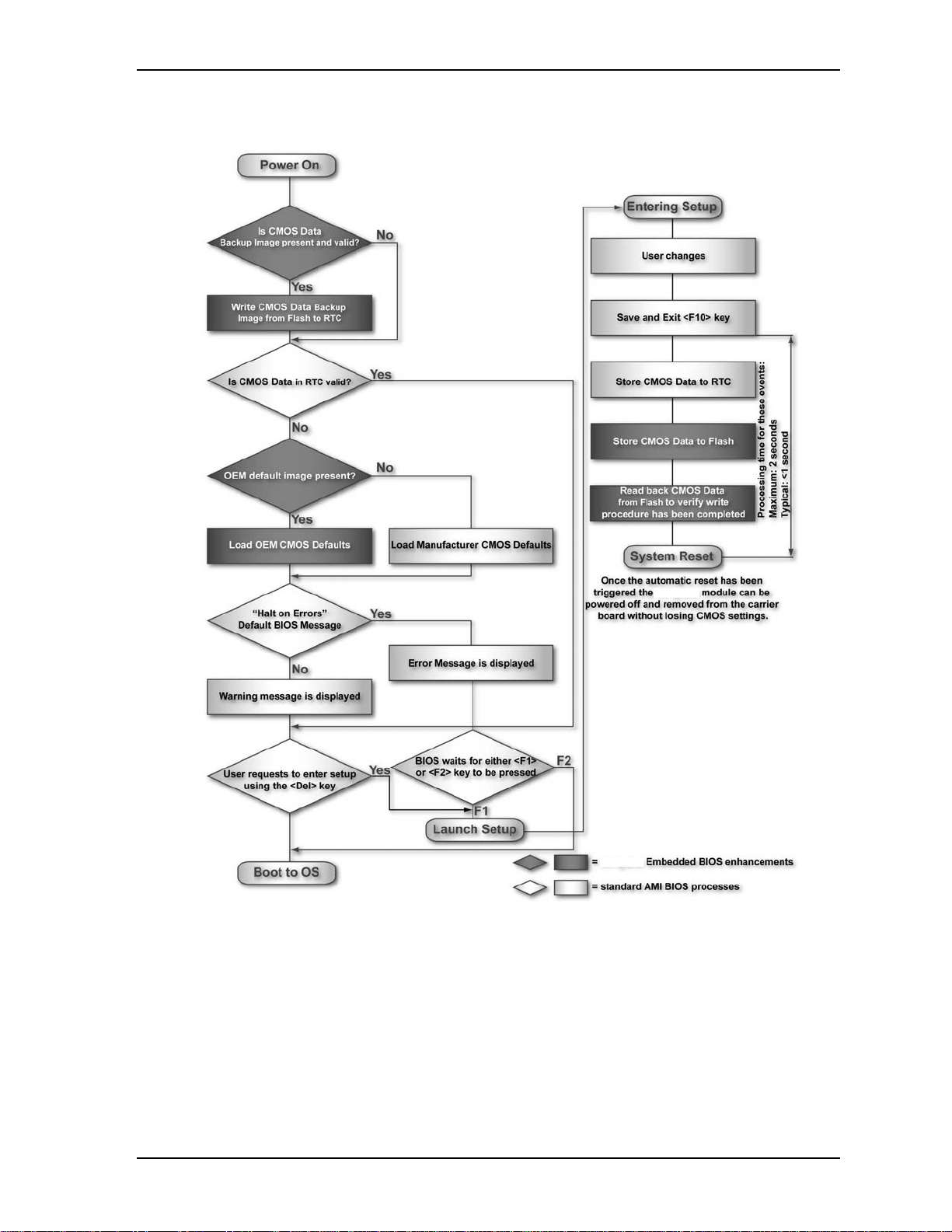
Simplified Overview of BIOS Setup Data Backup
Ampro,
Ampro
The above diagram provides an overview of how the BIOS Setup Data is backed up on modules. OEM
default values mentioned above refer to customer specific CMOS settings created using the System Utility
tool.
Once the BIOS Setup Program has been entered and the settings have been changed, the user saves the
settings and exits the BIOS Setup Program using the F10 key feature. After the F10 function has been
evoked, the CMOS Data is stored in a dedicated non-volatile CMOS Data Backup area located in the BIOS
Flash Memory chip as well as RTC. The CMOS Data is written to and read back from the CMOS Data
Backup area and verified. Once verified the F10 Save and Exit function continues to perform some minor
processing tasks and finally reaches an automatic reset point, which instructs the module to reboot. After the
Automatic Reset has been triggered the module can be powered off and if need be removed from the
baseboard without losing the new CMOS settings.
COM 830 Reference Manual 17
Page 24

Chapter 2 Specifications
Security Features
The COM 830 can be equipped optionally with a “Trusted Platform Module” (TPM 1.2). This TPM 1.2
includes co-processors to calculate efficient hash and RSA algorithms with key lengths up to 2,048 bits as
well as a real random number generator. Security sensitive applications like gaming and e-commerce will
benefit also with improved authentication, integrity and confidence levels.
Suspend to Ram
The Suspend to RAM feature is available on the COM 830.
Ampro Tech Notes
The COM 830 has some technological features that require additional explanation. The following section
will give the reader a better understanding of some of these features. This information will also help to gain
a better understanding of the information found in the System Resources section of this manual as well as
some of the setup nodes found in the BIOS Setup Program description section.
Comparison of I/O APIC to 8259 PIC Interrupt mode
I/O APIC (Advanced Programmable Interrupt controller) mode deals with interrupts differently than the
8259 PIC.
The method of interrupt transmission used by APIC mode is implemented by transmitting interrupts through
the system bus and they are handled without the requirement of the processor to perform an interrupt
acknowledge cycle.
Another difference between I/O APIC and 8259 PIC is the way the interrupt numbers are prioritized. Unlike
the 8259 PIC, the I/O APIC interrupt priority is independent of the actual interrupt number.
A major advantage of the I/O APIC found in the chipset of the COM 830 is that it's able to provide more
interrupts, a total of 24 to be exact. It must be mentioned that the APIC is not supported by all operating
systems. In order to utilize the APIC mode it must be enabled in the BIOS setup program before the
installation of the OS and it only functions in ACPI mode. You can find more information about APIC in the
IA-32 Intel Architecture Software Developer's Manual, Volume 3 in chapter 8.
NOTE You must ensure that your operating system su pports APIC mode in order to use it.
Intel® Matrix Storage Technology
The ICH7M-DH provides support for Intel® Matrix Storage Technology, providing both AHCI and
integrated RAID functionality.
AHCI
The ICH7M-DH provides hardware support for Advanced Host Controller Interface (AHCI), a new
programming interface for SATA host controllers. Platforms supporting AHCI may take advantage of
performance features such as no master/slave designation for SATA devices (each device is treated as a
master) and hardware-assisted native command queuing. AHCI also provides usability enhancements such
as Hot-Plug.
RAID
The industry-leading RAID capability provides high performance RAID 0 and 1 functionality on the 2
SATA ports of ICH7M-DH. Software components include an Option ROM for pre-boot configuration and
boot functionality, a Microsoft* Windows* compatible driver, and a user interface for configuration and
management of the RAID capability of ICH7M-DH.
18 Reference Manual COM 830
Page 25

Chapter 2 Specifications
Native vs. Compatible IDE mode
Compatible Mode
When operating in compatible mode, the SATA and PATA (Parallel ATA) controller together need two
legacy IRQs (14 and 15) and are unable to share these IRQs with other devices. This is a result of the fact
that the SATA and PATA controller emulate legacy IDE controllers.
Native Mode
Native mode allows the SATA and PA TA controllers to operate as true PCI devices and therefore do not need
dedicated legacy resources, which means it can be configured anywhere within the system. When either the
SATA or PATA controll er runs in native mode it only requires one PCI interrupt for both channels and also
has the ability to share this interrupt with other devices in the system. Setting Enhanced mode in the BIOS
setup program will automatically enable Native mode as Native mode is a subset of Enhanced mode.
Running in native mode frees up interrupt resour ces (IRQs 14 and 15) and decreases the chance that there
may be a shortage of interrupts when installing devices.
NOTE If your operating system supports native mode then Ampro recommends you
enable it.
Intel® Processor Features
Thermal Monitor and Catastrophic Thermal Protection
Intel® Core™ 2 Duo, Core™ Duo and Celeron M processors have a thermal monitor feature that helps to
control the processor temperature. The integrated TCC (Thermal Control Circuit) activates if the processor
silicon reaches its maximum operating temperature. The activation temperature, that the Intel Thermal
Monitor uses to activate the TCC, cannot be configured by the user nor is it software visible.
The Thermal Monitor can control the processor temperature through the use of two different methods
defined as TM1 and TM2. TM1 method consists of the modulation (starting and stopping) of the processor
clocks at a 50% duty cycle. The TM2 method initiates an Enhanced Intel Speedstep transition to the lowest
performance state once the processor silicon reaches the maximum operating temperature.
NOTE The maximum operating temperature for Intel Core™ 2 Duo, Core™ Duo and
Celeron M processors is 100°C. TM2 mode is used for Intel Core 2 Duo and
Core Duo processors, it is not supported by Intel Celeron M processors.
Two modes are supported by the Thermal Monitor to activate the TCC. They are called Automatic and OnDemand. No additional hardware, software, or handling routines are necessary when using Autom atic
Mode.
NOTE T o ensure that the TCC is active for only short periods of time thus reducing the
impact on processor performance to a minimum, it is necessary to have a
properly designed thermal solution. The Intel Core 2 Duo, Core™ Duo and
Celeron M processor's respective datasheet can provide you with more
information about this subject.
THERMTRIP# signal is used by Intel's Intel Core 2 Duo, Core Duo and Celeron M processors for
catastrophic thermal protection. If the processor's silicon reaches a temperature of approximately 125°C then
the processor signal THERMTRIP# will go active and the system will automatically shut down to prevent
COM 830 Reference Manual 19
Page 26

Chapter 2 Specifications
any damage to the processor as a result of overheating. The THERMTRIP# signal activation is completely
independent from processor activity and therefore does not produce any bus cycles.
NOTE In order for THERMTRIP# to be able to automatically switch off the system it is
necessary to use an ATX style power supply.
Processor Performance Control
Intel® Core™ 2 Duo and Core™ Duo processors run at different voltage/frequency states (performance
states), which is referred to as Enhanced Intel
®
SpeedStep® technology (EIST). Operating systems that
support performance control take advantage of microprocessors that use several different performance states
in order to efficiently operate the processor when it is not being fully utilized. The operating system will
determine the necessary performance state that the processor should run at so that the optimal balance
between performance and power consumption can be achieved during runtime.
The Windows family of operating systems links its processor performance control policy to the power
scheme setting found in the control panel option applet.
NOTE If the “Home/Office” or “Always On” power scheme is selected when using
Windows operating systems then the processor will always run at the highest
performance state. For more information about this subject see chapter 8 of the
ACPI Specification Revision 2.0c, which can be found at www.acpi.info. Also
visit Microsoft's website and search for the document called “Windows Native
Processor Performance Control”.
The Ampro BIOS allows you to limit the maximum processor frequency . This can be useful if the maximum
performance is not required or if the maximum processor perform ance state dissipates too much power and
heat.
In the 'CPU Configuration' submenu of the 'BIOS Setup Program' you'll find the node for 'Max. Frequency'
limitation. For each Intel Core 2 Duo and Core Duo processor the BIOS lists the supported frequencies. If a
lower frequency than the maximum one is selected, the processor will never run at frequencies above this
setting.
Celeron M processors do not support Enhanced Intel SpeedStep
®
technology. They always run at a fixed
frequency. In order to limit the performance and power consumption of Celeron M processors, the BIOS
offers 'On-Demand Clock Modulation' support in the 'CPU Configuration' submenu of the 'BIOS Setup
Program'. When 'On-Demand Clock Modulation' is enabled, the processor clock is throttled using the duty
cycle determined in setup. Keep in mind that the 'On-Demand' clock modulation duty cycle indicates that the
clock on to clock off interval ratio. This means that when set to 75% the clock is running 75% of the overall
time and this leads to a performance decrease of approximately 25%.
Intel 64
The formerly known Intel Extended Memory 64 Technology is an enhancement to Intel's IA-32 architecture.
Intel 64 is only available on Core 2 Duo processors and is designed to run newly written 64-bit code and
access more than 4GB of memory. Processors with Intel 64 architecture support 64-bit-capable operating
systems from Microsoft and Red Hat. Processors running in legacy mode remain fully compatible with
today's existing 32-bit applications and operating systems.
Platforms with Intel 64 can be run in three basic ways:
1. Legacy Mode: 32-bit operating system and 32-bit applicat ion s. In th is mod e no software changes are
required, however the benefits of Intel 64 are not utilized.
2. Compatibility Mode: 64-bit operating system and 32 -bi t appl ications. This mode requires all device
drivers to be 64-bit. The operating system will see the 64-bit extensio ns but the 32-bit application will
not. Existing 32-bit applications do not need to be recompiled and may or may not benefit from the 64bit extensions. The application will likely need to be re-certified by the vendor to run on the new 64-bit
extended operating system.
20 Reference Manual COM 830
Page 27

Chapter 2 Specifications
3. 64-bit Mode: 64-bit operating system and 64-bit applications. This usage requires 64-bit device drivers.
It also requires applications to be modified for 64-bit operation and then recompiled and validated.
Intel 64 provides support for:
64-bit flat virtual address space
64-bit pointers
64-bit wide general purpose registers
64-bit integer support
Up to one Terabyte (TB) of platform address space
You can find more information about Intel 64 Technology at: http://developer.intel.com/technology/intel64/
index.htm
NOTE Ampro does not intend to offer BSPs for 64-bit operating systems. Contact
technical support if you plan to use a 64-bit operating system on the COM 830.
Intel® Virtualization Technology
Virtualization solutions enhanced by Intel VT will allow a Core Duo and Core 2 Duo platform to run
multiple operating systems and applications in independent partitions. When using virtualization
capabilities, one computer system can function as multiple "virtual" systems. With processor and I/O
enhancements to Intel's various platforms, Intel Virtualization T echnology can improve the performance and
robustness of today's software-only virtual machine solutions.
Intel VT is a multi-generational series of extensions to Intel processor and platform architecture that
provides a new hardware foundation for virtualization, establishing a common infrastructure for all classes
of Intel based systems. The broad availability of Intel VT makes it possible to create entirely new
applications for virtualization in servers, clients as well as embedded systems thus providing new ways to
improve system reliability, manageability, security, and real-time quality of service.
The success of any new hardware architecture is highly dependent on the system software that puts its new
features to use. In the case of virtualization technology, that support comes from the virtual machine monitor
(VMM), a layer of software that controls the underlying physical platform resources sharing them between
multiple "guest" operating systems. Intel VT is already incorporated into most commercial and open-source
VMMs including those from VMware, Microsoft, XenSource, Parallels, Virtual Iron, Jaluna and TenAsys.
You can find more information about Intel Virtualization Technology at: http:// developer.intel.com/
technology/virtualization/index.htm
NOTE Ampro does not offer virtual machine monitor (VMM) software. All VMM
software support questions and queries should be directed to the VMM software
vendor and not technical support.
Thermal Management
ACPI is responsible for allowing the operating system to play an important part in the system's thermal
management. This results in the operating system having the ability to take control of the operating
environment by implementing cooling decisions according to the demands put on the CPU by the
application.
The COM 830 ACPI thermal solution offers three different cooling policies.
Passive Cooling
When the temperature in the thermal zone must be reduced, the operating system can decrease the power
consumption of the processor by throttling the processor clock. One of the advantages of this cooling policy
is that passive cooling devices (in this case the processor) do not produce any noise. Use the “passive
cooling trip point” setup node in the BIOS setup program to determine the temperature threshold that the
operating system will use to start or stop the passive cooling procedure.
COM 830 Reference Manual 21
Page 28

Chapter 2 Specifications
Active Cooling
During this cooling policy the operating system is turning the fan on/off. Although active cooling devices
consume power and produce noise, they also have the ability to cool the thermal zone without having to
reduce the overall system performance. Use the “active cooling trip point” setup node in the BIOS setup
program to determine the temperature threshold that the operating system will use to start the active cooling
device. It is stopped again when the temperature goes below the threshold (5°C hysteresis).
Critical Trip Point
If the temperature in the thermal zone reaches a critical point then the operating system will perform a
system shut down in an orderly fashion in order to ensure that there is no damage done to the system as
result of high temperatures. Use the “critical trip point” setup node in the BIOS setup program to determine
the temperature threshold that the operating system will use to shut down the system.
NOTE The end user must determine the cooling preferences for the system by using the
setup nodes in the BIOS setup program to establish the appropriate trip points.
If passive cooling is activated and the processor temperature is above the trip point the
processor clock is throttled according to the formula below.
ΔP[%] = TC1(T
ΔP is the performance delta
is the target temperature = critical trip point.
T
t
The two coefficients TC1 and TC2 and the sampling period TSP are hardware
dependent constants. These constants are set to fixed values for the COM 830:
TC1= 1
TC2= 5
TSP= 5 seconds
See section 12 of the ACPI Specification 2.0 C for more information about passive
cooling.
) + TC2(Tn-Tt)
n-Tn-1
ACPI Suspend Modes and Resume Events
COM 830 supports the S1 (POS= Power On Suspend) state and S3 (STR= Suspend to RAM). For more
information about S3 wake events see section “ACPI Configuration Submenu”.
S4 (Suspend to Disk) is not supported by the BIOS (S4_BIOS) but it is supported by the following operating
systems (S4_OS= Hibernate):
Win2K
WinXP
The following table lists the “Wake Events” that resume the system from both S1 or S3 unless otherwise
stated in the “Conditions/Remarks” column:
Wake Event Conditions/Remarks
Power Button Wakes unconditionally from S1-S5.
GPI1# Only if configured as Lid Switch in the ACPI setup menu. Additionally the
lid button has to be activated using the Windows Power Options. The best
way to use it is to go to Standby (see note below) on lid button press and
wake from Standby (see note below) on lid button release.
22 Reference Manual COM 830
Page 29
Chapter 2 Specifications
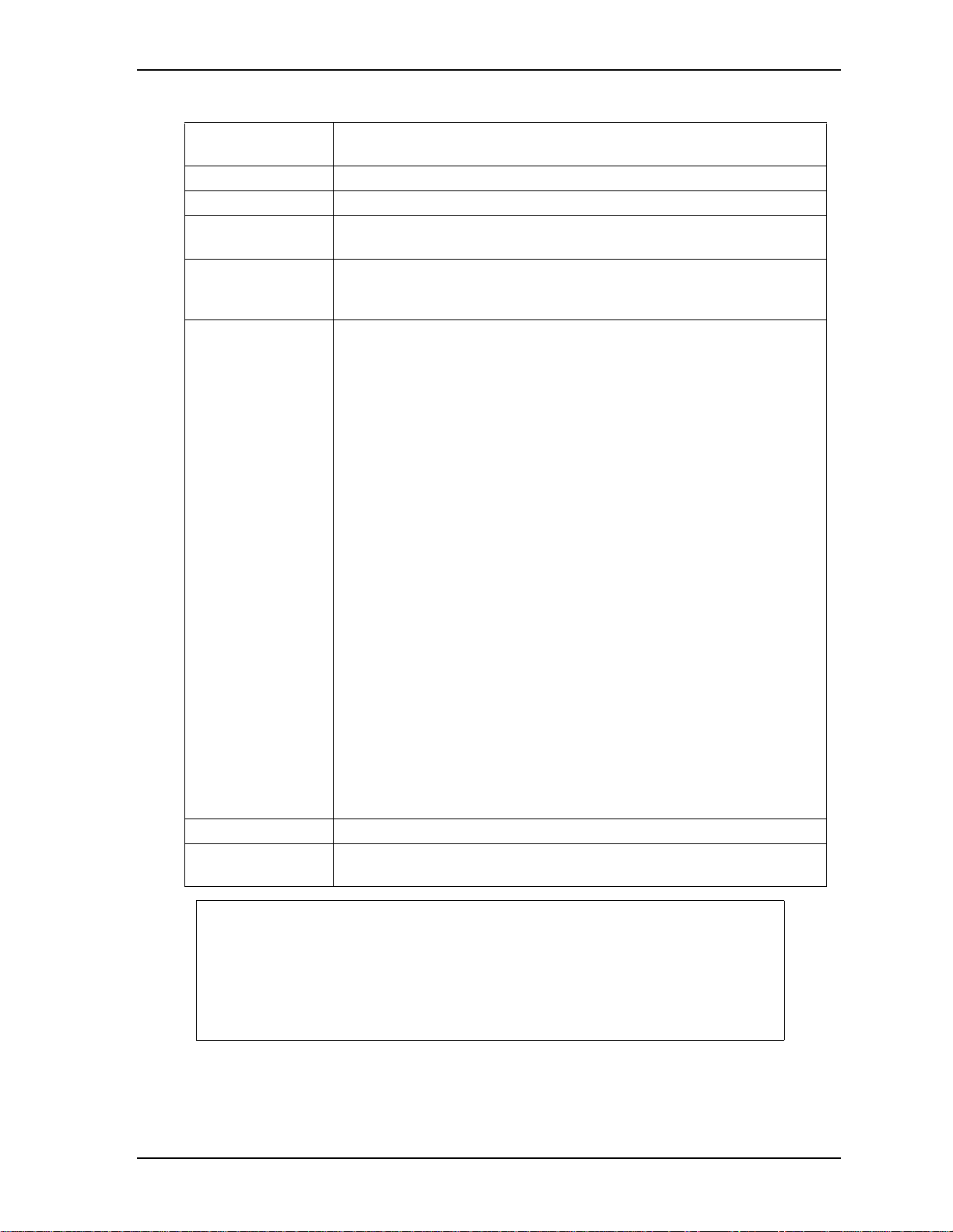
GPI2# Set GPE2 Function node to Sleep Button in the ACPI setup menu or set
Resume On Ring to Enabled in the Power setup menu.
Onboard LAN Event Device driver must be configured for Wake On LAN support.
SMBALERT# Wakes unconditionally from S1-S5.
PCI Express
Wakes unconditionally from S1-S3.
WAKE#
PME# A ctivat e the wake up capabi lities of a PCI device using Windows Device
Manager configuration options for this device OR set Resume On PME# to
Enabled in the Power setup menu.
USB Mouse/
Keyboard Event
When Standby mode is set to S1, no special action must be taken for a USB
Mouse/Keyboard Event to be used as a Wake Event.
When Standby mode is set to S3, the following must be done for a USB
Mouse/Keyboard Event to be used as a Wake Event.
USB Hardware must be powered by standby power source.
Set USB Device Wakeup from S3/S4 to ENABLED in the ACPI setup menu.
Under Windows XP add following registry entries:
Add this key:
HKEY_LOCAL_MACHINE\SYSTEM\CurrentControlSet\Services\usb
Under this key add the following value:
“USBBIOSx“=DWORD:00000000
Note that Windows XP disables USB wakeup from S3, so this entry has to be
added to re-enable it.
Configure USB keyboard/mouse to be able to wake up the system:
In Device Manager look for the keyboard/mouse devices. Go to the Power
Management tab and check 'Allow this device to bring the computer out of
standby'.
Note: When the standby state is set to S3 in the ACPI setup menu, the power
management tab for USB keyboard /mouse devices only becomes available
after adding the above registry entry and rebooting to allow the registry
changes to take affect.
RTC Alarm Activate and configure Resume On RTC Alarm in the Power setup menu.
Watchdog Power
Wakes unconditionally from S1-S5.
Button Event
NOTE The above list has been verified using a Windows XP SP2 ACPI enabled
installation.
When using Windows XP, Standby mode is either an S1 state or S3 state
depending on what has been selected in the ACPI Configuration Menu in the BIOS
setup program.
COM 830 Reference Manual 23
Page 30
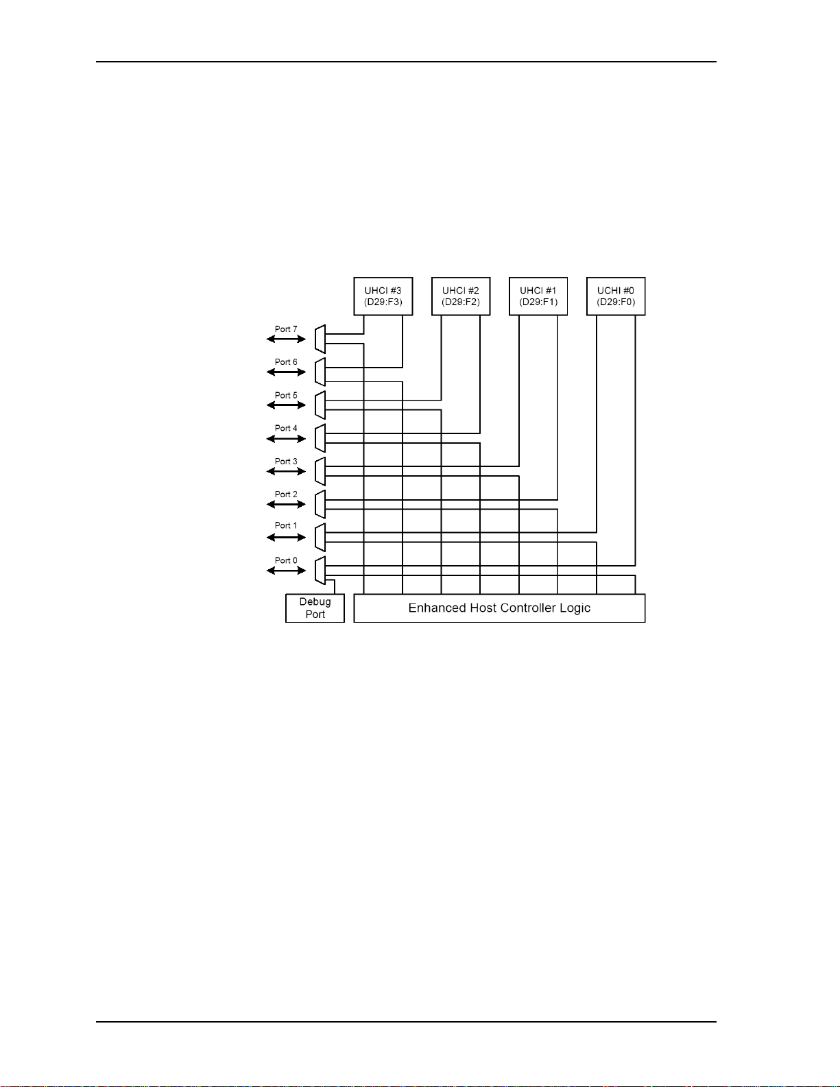
Chapter 2 Specifications
USB 2.0 EHCI Host Controller Support
The 8 USB ports are shared between an EHCI host controller and the 4 UHCI host controllers.
Within the EHC functionality there is a port-routing logic that executes the mixing between the two different
types of host controllers (EHCI and UHCI). This means that when a USB device is connected the routing
logic determines who owns the port. If the device is not USB 2.0 compliant, or if the software drivers for
EHCI support are not installed, then the UHCI controller owns the ports.
Routing Diagram:
24 Reference Manual COM 830
Page 31

Chapter 3 Signals and Pinout Tables
The following section describes the signals found on COM Express™ Type II connectors used for Ampro
modules.
The table below describes the terminology used in this section for the Signal Description tables. The PU/PD
column indicates if a COM Express internal pull-up or pull-down resistor has been used. If the field entry
area in this column for the signal is empty, then no pull-up or pull-down resistor has been implemented.
The “#” symbol at the end of the signal name indicates that the active or asserted state occurs when the
signal is at a low voltage level. When “#” is not present, the signal is asserted when at a high voltage level.
Table 3-1. Signal Tables Terminology Descriptions
Term Description
PU COM Express internally implement e d Pull up resistor
PD COM Express internally implement ed Pull down resistor
I/O 3.3V Bi-directional signal 3.3V tolerant
I/O 5V Bi-directional signal 5V tolerant
I 3.3V Input 3.3V tolerant
I 5V Input 5V tolerant
I/O 3.3VSB Input 3.3V tolerant active in standby state
O 3.3V Output 3.3V signal level
O 5V Output 5V signal level
OD Open drain output
P Power Input/Output
DDC Display Data Channel
PCIE In compliance with PCI Express Base Specification, Revision 1.0a
SATA In compliance with Serial ATA specificati on, Revisio n 1.0a
REF Reference voltage output. May be sourced from a module power plane.
PDS Pull-down strap. A module output pin that is either tied to GND or is not connected.
Used to signal module capabilities (pinout type) to the Carrier Board.
COM 830 Reference Manual 25
Page 32

Chapter 3 Signals and Pinout Tables
A-B Connector Signal Descriptions
Table 3-2. AC'97/Intel® High Definition Audio Link Signals Descriptions
Signal Description
AC_RST# AC ’97/Intel High Definition Audio Reset: This
signal is the master hardware reset to external codec(s).
AC_SYNCAC ’97/Intel High Definition Audio Sync: This signal
is a 48 kHz fixed rate sample sync to the codec(s). It is
also used to encode the stream number.
AC_BIT_
CLK
AC_SDOUTAC ’97/Intel High Definition Audio Serial Data Out:
AC_SDIN
[2:0]
AC ’97 Bit Clock Input: This signal is a 12.288 MHz
serial data clock generated by the external codec(s).
This signal has an Intel integrated pull-down resistor.
Intel High Definition Audio Bit Clock Output: This
signal is a 24.000MHz serial data clock generated by
the Intel High Definition Audio controller (the Intel
ICH7M-DH). This signal has an Intel
down resistor so that AC_BIT_CLK doesn’t float when
an Intel High Definition Audio codec (or no codec) is
connected but the signals are temporarily configured as
AC ’97.
This signal is the serial TDM data output to the
codec(s). This serial output is double-pumped for a bit
rate of 48 Mb/s for Intel High Definition Audio.
AC ’97//Intel High Definition Audio Serial Data In
[0]: These signals are serial TDM data inputs from the
three codecs. The serial input is single-pumped for a bit
rate of 24 Mb/s for Intel High Definition Audio.
integrated pull-
I/O PU/PD Comment
O 3.3V
O 3.3V AC_S Y N
C is a boot
strap
signal (see
note
below)
I 3.3V
O 3.3V
O 3.3V AC_S D O
UT is a
boot strap
signal (see
note
below)
I 3.3V
NOTE Some signals have special functionality during the reset process. They may bootstrap
some basic important functions of the module.
26 Reference Manual COM 830
Page 33
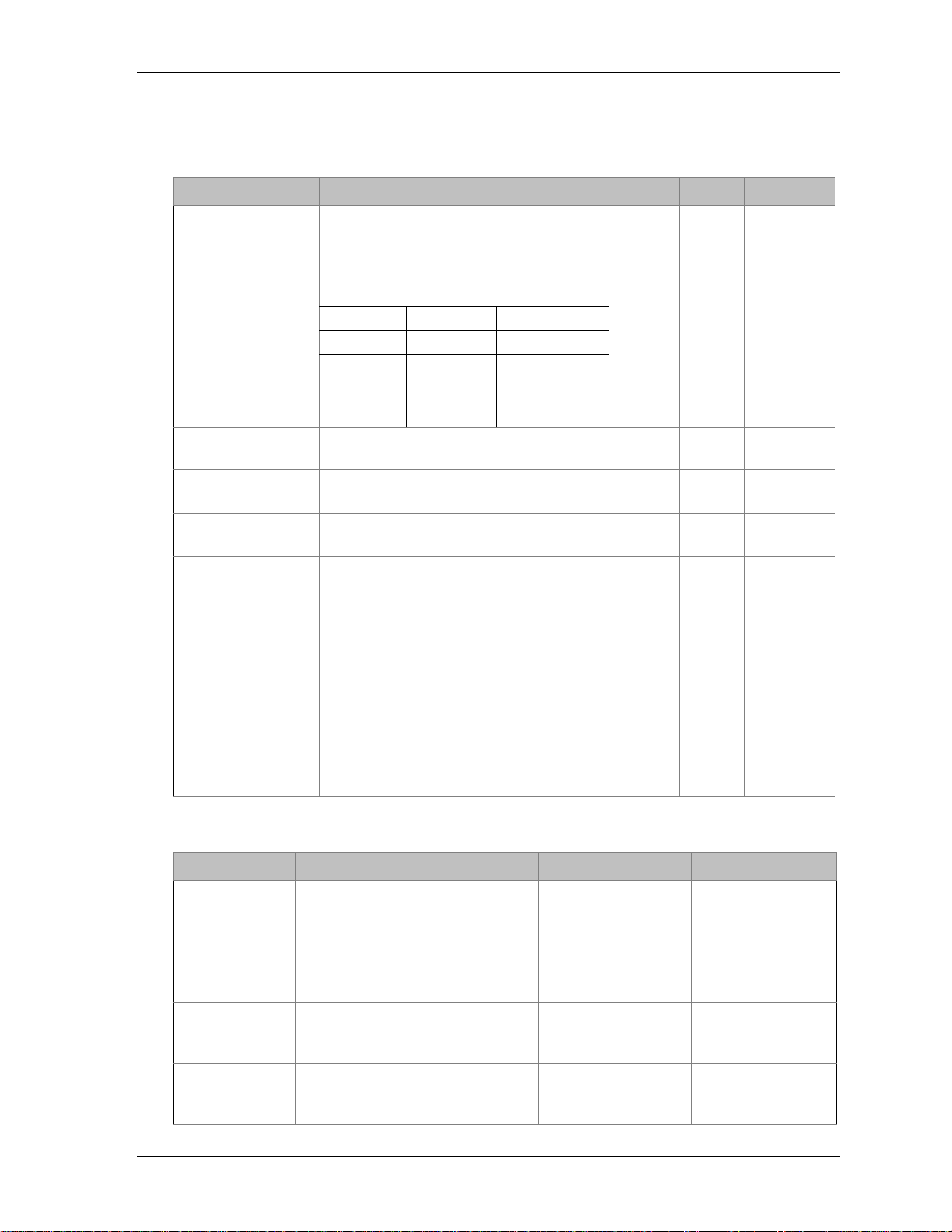
Chapter 3 Signals and Pinout Tables
AC_SYNC and AC_SDOUT can be used to switch PCI Express channels 1-4 between x1 and x4 mode. If
both signals are each pulled-up (using 1k resistors) to 3.3V at the rising edge of PWROK then x4 mode is
enabled. x1 mode is used by default if these resistors are not populated.
Table 3-3. Gigabit Ethernet Signal Descriptions
Gigabit Ethernet Description I/O PU/PD Comment
GBE0_MDI[0:3]+
GBE0_MDI[0:3]-
Gigabit Ethernet Controller 0: Media
Dependent Interface Differential Pairs 0, 1,
2, 3. The MDI can operate in 1000, 100, and
10Mbit/sec modes. Some pairs are unused
I/O
Analog
Twisted
pair signals
for external
transformer.
in some modes according to the following:
1000 100 10
MDI[0]+/- B1_DA+/- TX+/- TX+/MDI[1]+/- B1_DB+/- RX+/- RX+/MDI[2]+/- B1_DC+/MDI[3]+/- B1_DD+/-
GBE0_ACT# Gigabit Ethernet Controller 0 activity
OD
indicator, active low.
GBE0_LINK# Gigabit Ethernet Controller 0 link indicator,
OD
active low.
GBE0_LINK100# Gigabit Ethernet Controller 0 100Mbit/sec
OD
link indicator, active low.
GBE0_LINK1000# Gigabit Ethernet Controller 0 1000Mbit/sec
OD
link indicator, active low.
GBE0_CTREF Reference voltage for Carrier Board
Ethernet channel 0 magnetics center tap.
The reference voltage is determined by the
requirements of the module PHY and may
REF Reference
voltage on
COM 830
is 1.8V
be as low as 0V and as high as 3.3V.
The reference voltage output shall be
current limited on the module. In the case in
which the reference is shorted to ground,
the current shall be limited to 250mA or
less.
Table 3-4. Serial ATA Signal Descriptions
Signal Description I/O PU/PD Comment
SATA0_RX+
SATA0_RX-
SATA0_TX+
SATA0_TX-
SATA1_RX+
SATA1_RX-
SATA1_TX+
SATA1_TX-
Serial A TA channel 0, Receive Input
differential pair.
Serial ATA channel 0, Transmit
Output differential pair.
Serial A TA channel 1, Receive Input
differential pair.
Serial ATA channel 1, Transmit
Output differential pair.
I SATA Supports Serial ATA
O SATA Supports Serial ATA
I SATA Supports Serial ATA
O SATA Supports Serial ATA
specification,
Revision 1.0a
specification,
Revision 1.0a
specification,
Revision 1.0a
specification,
Revision 1.0a
COM 830 Reference Manual 27
Page 34

Chapter 3 Signals and Pinout Tables
Table 3-4. Serial ATA Signal Descriptions (Continued)
SATA2_RX+
SATA2_RX-
SATA2_TX+
SATA2_TX-
SATA3_RX+
SATA3_RX-
SATA3_TX+
SATA3_TX-
ATA_ACT# ATA (parallel and serial) or SAS
Serial A TA channel 2, Receive Input
differential pair.
Serial ATA channel 2, Transmit
Output differential pair.
Serial A TA channel 3, Receive Input
differential pair.
Serial ATA channel 3, Transmit
Output differential pair.
activity indicator, active low.
I SATA Not supported
O SATA Not supported
I SATA Not supported
O SATA Not supported
OC 3.3V ATA_ACT# is a
boot strap signal
(see note below)
NOTE Some signals have special functionality during the reset process. They may
bootstrap some basic important functions of the module.
Table 3-5. PCI Express Signal Descriptions [general purpose]
Signal Description I/O PU/PD Comment
PCIE0_RX+
PCIE0_RX-
PCI Express channel 1, Receive Input
differential pair
I
PCIE
Supports PCI
Express Base
Specification,
Revision 1.0a
PCIE0_TX+
PCIE0_TX-
PCI Express channel 1, Transmit Output
differential pair
O
PCIE
Supports PCI
Express Base
Specification,
Revision 1.0a
PCIE1_RX+
PCIE1_RX-
PCI Express channel 2, Receive Input
differential pair
I
PCIE
Supports PCI
Express Base
Specification,
Revision 1.0a
PCIE1_TX+
PCIE1_TX-
PCI Express channel 2, Transmit Output
differential pair
O
PCIE
Supports PCI
Express Base
Specification,
Revision 1.0a
PCIE2_RX+
PCIE2_RX-
PCI Express channel 3, Receive Input
differential pair
I
PCIE
Supports PCI
Express Base
Specification,
Revision 1.0a
PCIE2_TX+
PCIE2_TX-
PCI Express channel 3, Transmit Output
differential pair
O
PCIE
Supports PCI
Express Base
Specification,
Revision 1.0a
PCIE3_RX+
PCIE3_RX-
PCI Express channel 4, Receive Input
differential pair
I
PCIE
Supports PCI
Express Base
Specification,
Revision 1.0a
28 Reference Manual COM 830
Page 35

Chapter 3 Signals and Pinout Tables
Table 3-5. PCI Express Signal Descriptions [general purpose] (Continued)
PCIE3_TX+
PCIE3_TX-
PCI Express channel 4, Transmit Output
differential pair
O
PCIE
Supports PCI
Express Base
Specification,
Revision 1.0a
PCIE4_RX+
PCIE4_RX-
PCI Express channel 5, Receive Input
differential pair
I
PCIE
Supports PCI
Express Base
Specification,
Revision 1.0a
PCIE4_TX+
PCIE4_TX-
PCI Express channel 5, Transmit Output
differential pair
O
PCIE
Supports PCI
Express Base
Specification,
Revision 1.0a
PCIE5_RX+
PCIE5_RX-
PCI Express channel 6, Receive Input
differential pair
I
PCIE
Not available.
Used by
onboard Gigabit
Ethernet.
PCIE5_TX+
PCIE5_TX-
PCI Express channel 6, Transmit Output
differential pair
O
PCIE
Not available.
Used by
onboard Gigabit
Ethernet.
PCIE_CLK_RE
F+
PCIE_CLK_RE
PCI Express Reference Clock output for all
PCI Express and PCI Express Graphics
Lanes
O
PCIE
PD 49.9R
F-
T able 3-6. ExpressCard Support Pins Descriptions
Signal Description I/O PU/PD Comment
EXCD[0..1]_CPPE#ExpressCard capable card
request
EXCD[0..1]_RST#
ExpressCard Reset O 3.3V PU 10k
(EXCD[0..1]_PER
I
3.3VSB
PU 8k2
3.3VSB
3.3V
ST#)
Table 3-7. LPC Signal Descriptions
Signal Description I/O PU/PD Comment
LPC_AD[0:3] LPC multiplexed address, command and
I/O 3.3V
data bus
LPC_FRAME# LPC frame indicates the start of an LPC
O 3.3V
cycle
LPC_DRQ[0:1]# LPC serial DMA request I 3.3V PU 10k
3.3V
LPC_SERIRQ LPC serial int e rrupt I/O 3.3V PU 10k
3.3V
LPC_CLK LPC clock output - 33MHz nominal O 3.3V
COM 830 Reference Manual 29
Page 36

Chapter 3 Signals and Pinout Tables
Table 3-8. USB Signal Descriptions
Signal Description I/O PU/PD Comment
USB0+ USB Port 0, data + or D+ I/O USB 2.0 compliant and
backwards compatible
to USB 1.1
USB0- USB Port 0, data - or D- I/O USB 2.0 compliant and
backwards compatible
to USB 1.1
USB1+ USB Port 1, data + or D+ I/O USB 2.0 compliant and
backwards compatible
to USB 1.1
USB1- USB Port 1, data - or D- I/O USB 2.0 compliant and
backwards compatible
to USB 1.1
USB2+ USB Port 2, data + or D+ I/O USB 2.0 compliant and
backwards compatible
to USB 1.1
USB2- USB Port 2, data - or D- I/O USB 2.0 compliant and
backwards compatible
to USB 1.1
USB3+ USB Port 3, data + or D+ I/O USB 2.0 compliant and
backwards compatible
to USB 1.1
USB3- USB Port 3, data - or D- I/O USB 2.0 compliant and
backwards compatible
to USB 1.1
USB4+ USB Port 4, data + or D+ I/O USB 2.0 compliant and
backwards compatible
to USB 1.1
USB4- USB Port 4, data - or D- I/O USB 2.0 compliant and
backwards compatible
to USB 1.1
USB5+ USB Port 5, data + or D+ I/O USB 2.0 compliant and
backwards compatible
to USB 1.1
USB5- USB Port 5, data - or D- I/O USB 2.0 compliant and
backwards compatible
to USB 1.1
USB6+ USB Port 6, data + or D+ I/O USB 2.0 compliant and
backwards compatible
to USB 1.1
USB6- USB Port 6, data - or D- I/O USB 2.0 compliant and
backwards compatible
to USB 1.1
USB7+ USB Port 7, data + or D+ I/O USB 2.0 compliant and
backwards compatible
to USB 1.1
30 Reference Manual COM 830
Page 37

Chapter 3 Signals and Pinout Tables
Table 3-8. USB Signal Descriptions (Continued)
USB7- USB Port 7, data - or D- I/O USB 2.0 compliant and
backwards compatible
to USB 1.1
USB_0_1_OC# USB over-current sense,
USB ports 0 and 1. A pull-
I
3.3VSB
PU 10k
3.3VSB
up for this line shall be
present on the module. An
open drain driver from a
USB current monitor on
the carrier board may
drive this line low. Do not
pull this line high on the
carrier board.
USB_2_3_OC# USB over-current sense,
USB ports 2 and 3. A pull-
I
3.3VSB
PU 10k
3.3VSB
up for this line shall be
present on the module. An
open drain driver from a
USB current monitor on
the carrier board may
drive this line low. Do not
pull this line high on the
carrier board.
USB_4_5_OC# USB over-current sense,
USB ports 4 and 5. A pull-
I
3.3VSB
PU 10k
3.3VSB
up for this line shall be
present on the module. An
open drain driver from a
USB current monitor on
the carrier board may
drive this line low. Do not
pull this line high on the
carrier board.
USB_6_7_OC# USB over-current sense,
USB ports 6 and 7. A pull-
I
3.3VSB
PU 10k
3.3VSB
up for this line shall be
present on the module. An
open drain driver from a
USB current monitor on
the carrier board may
drive this line low. Do not
pull this line high on the
carrier board.
Table 3-9. CRT Signal Descriptions
Signal Description I/O PU/PD Comment
VGA_RED Red for monitor. Analog DAC output,
designed to drive a 37.5-Ohm equivalent load.
VGA_GRN Green for monitor. Analog DAC output,
designed to drive a 37.5-Ohm equivalent load.
O
Analog
O
Analog
PD 150R Analog output
PD 150R Analog output
COM 830 Reference Manual 31
Page 38
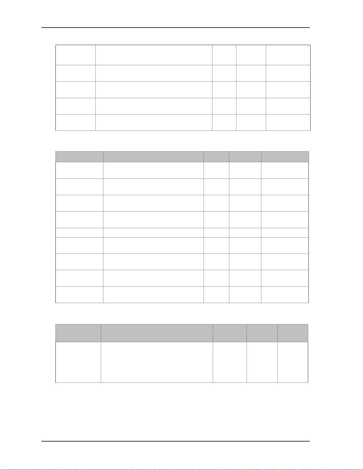
Chapter 3 Signals and Pinout Tables
Table 3-9. CRT Signal Descriptions (Continued)
VGA_BLU Blue for monitor. Analog DAC output,
designed to drive a 37.5-Ohm equivalent load.
O
Analog
PD 150R Analog output
VGA_HSYNC Horizontal sync output to VGA monitor O 3.3V
VGA_VSYNC Vertical sync output to V GA monitor O 3.3V
VGA_I2C_CK DDC clock line (I²C port dedicated to identify
VGA monitor capabilities)
VGA_I2C_D
DDC data line. I/O 5V PU 2k2
AT
Table 3-10. LVDS Signal Descriptions
I/O 5V PU 2k2
5V
5V
Signal Description I/O PU/PD Comment
LVDS_A[0:3]+
LVDS_A[0:3]-
LVDS_A_CK+
LVDS_A_CK-
LVDS_B[0:3]+
LVDS_B[0:3]-
LVDS_B_CK+
LVDS_B_CK-
LVDS Channel A differential pairs O
LVDS
LVDS Channel A differential clock O
LVDS
LVDS Channel B differential pairs O
LVDS
LVDS Channel B differential clock O
LVDS
LVDS_VDD_EN LVDS panel power enable O 3.3V PD 10k
LVDS_BKLT_EN LVDS panel backlight enable O 3.3V
LVDS_BKLT_C
TRL
LVDS_I2C_CK DDC lines used for flat panel detection
LVDS_I2C_DAT DDC lines used for flat panel detection
LVDS panel backlight brightness
control
and control.
and control.
O 3.3V
O 3.3V PU 2k2
3.3V
I/O
3.3V
PU 2k2
3.3V
Table 3-11. TV-Out Signal Descriptions
Signal Description I/O PU/PD Commen
t
TV_DAC_A TVDAC Channel A Output supports the
following: Composite video: CVBS
Component video: Chrominance (Pb) analog
O
Analog
PD 150R Analog
output
signal
S-Video: not used
32 Reference Manual COM 830
Page 39

Chapter 3 Signals and Pinout Tables
Table 3-11. TV-Out Signal Descriptions (Continued)
TV_DAC_B TVDAC Chann el B Outpu t su pports the
following: Composite video: not used
Component video: Luminance (Y) analog
O
Analog
PD 150R Analog
output
signal.
S-Video: Luminance analog signal.
TV_DAC_C TVDAC Chann el C Outpu t su pports the
following: Composite video: not used
Component: Chrominance (Pr) analog
O
Analog
PD 150R Analog
output
signal.
S-Video: Chrominance analog signal.
Table 3-12. Miscellaneous Signal Descriptions
Signal Description I/O PU/PD Comment
I2C_CK
General purpose I²C port clock output
O 3.3V PU 4k7
3.3V
I2C_DAT
General purpose I²C port data I/O line
SPKR Output for audio enunciator, the "speaker" in
PC-AT systems
I/O
3.3V
PU 4k7
3.3V
O 3.3V SPEAKER
is a boot
strap signal
(see note 1
below)
BIOS_DISABLE# Module BIOS disable input. Pull low to disable
module BIOS. Used to allow off-module BIOS
I 3.3V PU 4k7
3.3V
implementations.
WDT Output indicating that a watchdog time-out
event has occurred.
I 3.3V PU 10k
3.3V
This signal
is not
supported
(see note 2
below)
KBD_RST# Input to module from (optional) external
keyboard controller that can force a reset.
I PU 10k
3.3V
Pulled high on the module. This is a legacy
artifact of the PC-AT.
KBD_A20GATE Input to module from (optional) external
keyboard controller that can be used to control
I PU 10k
3.3V
the CPU A20 gate line. The A20GATE restricts
the memory access to the bottom megabyte and
is a legacy artifact of the PC-AT. Pulled low on
the module.
NOTE Some signals have special functionality during the reset process. They may
bootstrap some basic important functions of the module.
For more information about this signal, please visit Ask an Expert on the Ampro
web site.
COM 830 Reference Manual 33
Page 40

Chapter 3 Signals and Pinout Tables
Table 3-13. General Purpose I/O Signal Descriptions
Signal Description I/O PU/PD Commen
t
GPO[0] General purpose output pins. Upon a
hardware reset, these outputs should
O 3.3VSB PU 10k
3.3VSB
be low.
GPO[1] General purpose output pins. Upon a
hardware reset, these outputs should
O 3.3VSB PU 10k
3.3VSB
be low.
GPO[2] General purpose output pins. Upon a
hardware reset, these outputs should
O 3.3VSB PU 10k
3.3VSB
be low.
GPO[3] General purpose output pins. Upon a
hardware reset, these outputs should
O 3.3VSB PU 10k
3.3VSB
be low.
GPI[0] General purpose input pins. Pulled
high internally on the module.
GPI[1] General purpose input pins. Pulled
high internally on the module.
GPI[2] General purpose input pins. Pulled
high internally on the module.
GPI[3] General purpose input pins. Pulled
high internally on the module.
I 3.3VSB PU 10k
3.3VSB
I 3.3VSB PU 10k
3.3VSB
I 3.3VSB PU 10k
3.3VSB
I 3.3VSB PU 10k
3.3VSB
Table 3-14. Power and System Management Signal Descriptions
Signal Description I/O PU/PD Comment
PWRBTN# Power button to bring system out of S5 (soft
off), active on rising edge.
SYS_RESET#Reset button input. Active low input. System is
held in hardware reset while this input is low,
I 3.3VSB PU 10k
3.3VSB
I 3.3VSB PU 10k
3.3VSB
and comes out of reset upon release.
CB_RESET# Reset output from module to Carrier Board.
O 3.3V
Active low. Issued by module chipset and may
result from a low SYS_RESET# input, a low
PWR_OK input, a VCC_12V power input that
falls below the minimum specification, a
watchdog timeout, or may be initiated by the
module software.
PWR_OK Power OK from main power supply. A high
I 3.3V Set by
value indicates that the power is good.
SUS_STAT# Indicates imminent suspend operation; used to
notify LPC devices.
O 3.3VSB PU 10k
3.3VSB
resistor
divider to
accept
3.3V.
34 Reference Manual COM 830
Page 41

Chapter 3 Signals and Pinout Tables
Table 3-14. Power and System Management Signal Descriptions (Continued)
SUS_S3# Indicates system is in Suspend to RAM state.
Active low output. Also known as "PS_ON"
O 3.3VSB PU 10k
3.3VSB
and can be used to control an ATX power
supply.
SUS_S4# Indicates system is in Suspend to Disk state.
Active low output.
O 3.3VSB PU 10k
3.3VSB
Not
supported
SUS_S5# Indicates system is in Soft Off state. O 3.3VSB PU 10k
3.3VSB
WAKE0# PCI Express wake up signal. I 3.3VSB PU 10k
3.3VSB
WAKE1# General purpose wake up signal. May be used
to implement wake-up on PS/2 keyboard or
I 3.3VSB PU 10k
3.3VSB
mouse activity.
BATLOW# Battery low input. This signal may be driven
low by external circuitry to signal that the
I 3.3VSB PU 10k
3.3VSB
system battery is low, or may be used to signal
some other external power-management event.
THRM# Input from off-module temp sensor indicating
an over-temp situation.
THERMTRIP#Active low output indicating that the CPU has
entered thermal shutdown.
SMB_CK System Management Bus bidirectional clock
line. Power sourced through 5V standby rail
I 3.3V PU 10k
3.3V
O 3.3V PU 10k
3.3V
I/O
3.3VSB
PU 2k2
3.3VSB
and main power rails.
SMB_DAT# System Management Bus bidirectional data
line. Power sourced through 5V standby rail
I/O
3.3VSB
PU 2k2
3.3VSB
and main power rails.
SMB_ALERT#System Management Bus Alert – active low
input can be used to generate an SMI# (System
I 3.3VSB PU 10k
3.3VSB
Management Interrupt) or to wake the system.
Power sourced through 5V standby rail and
main power rails.
Table 3-15. Power and GND Signal Descriptions
Signal Description I/O PU/
Comment
PD
VCC_12V Primary power input: +12V nominal. All
P
available VCC_12V pins on the connector(s)
shall be used.
VCC_5V_SBY Standby power input: +5.0V nominal. If
P
VCC5_SBY is used, all available
VCC_5V_SBY pins on the connector(s) shall
be used. Only used for standby and suspend
functions. May be left unconnected if these
functions are not used in the system design.
COM 830 Reference Manual 35
Page 42

Chapter 3 Signals and Pinout Tables
Table 3-15. Power and GND Signal Descriptions
VCC_RTC Real-time clock circuit-power input. Nominally
+3.0V.
GND Ground - DC power and signal and AC signal
return path.
All available GND connector pins shall be used
and tied to Carrier Board GND plane.
P
P
A-B Connector Pinout
Table 3-16. Connector A-B Pinout
Pin Row A Pin Row B Pin Row A Pin Row B
A1 GND (FIXED) B1 GND (FIXED) A56 PCIE_TX4- B56 PCIE_RX4A2 GBE0_MDI3- B2 GBE0_ACT# A57 GND B57 GPO2
A3 GBE0_MDI3+ B3 LPC_FRAME# A58 PCIE_TX3+ B58 PCIE_RX3
+
A4 GBE0_LINK100# B4 LPC_AD0 A59 PCIE_TX3- B59 PCIE_RX3A5 GBE0_LINK1000# B5 LPC_AD1 A60 GND (FIXED) B60 GND
(FIXED)
A6 GBE0_MDI2- B6 LPC_AD2 A61 PCIE_TX2+ B61 PCIE_RX2
+
A7 GBE0_MDI2+ B7 LPC_AD3 A62 PCIE_TX2- B62 PCIE_RX2A8 GBE0_LINK# B8 LPC_DRQ0# A63 GPI1 (*) B63 GPO3
A9 GBE0_MDI1- B9 LPC_DRQ1# A64 PCIE_TX1+ B64 PCIE_RX1
+
A10 GBE0_MDI1+ B10 LPC_CLK A65 PCIE_TX1- B65 PCIE_RX1-
A11 GND (FIXED) B11 GND (FIXED) A66 GND B66 WAKE0#
A12 GBE0_MDI0- B12 PWRBTN# A67 GPI2 B67 WAKE1#
A13 GBE0_MDI0+ B13 SMB_CK A68 PCIE_TX0+ B68 PCIE_RX0
+
A14 GBE0_CTREF B14 SMB_DAT A69 PCIE_TX0- B69 PCIE_RX0-
A15 SUS_S3# B15 SMB_ALERT# A70 GND (FIXED) B70 GND
(FIXED)
A16 SATA0_TX+ B16 SATA1_TX+ A71 LVDS_A0+ B71 LVDS_B0+
A17 SATA0_TX- B17 SATA1_TX- A72 LVDS_A0- B72 LVDS_B0-
A18 SUS_S4# (*) B18 SUS_STAT# A73 LVDS_A1+ B73 LVDS_B1+
A19 SATA0_RX+ B19 SATA1_RX+ A74 LVDS_A1- B74 LVDS_B1-
36 Reference Manual COM 830
Page 43

Chapter 3 Signals and Pinout Tables
Table 3-16. Connector A-B Pinout (Continued)
A20 SATA0_RX- B20 SATA1_RX- A75 LVDS_A2+ B75 LVDS_B2+
A21 GND (FIXED) B21 GND (FIXED) A76 LVDS_A2- B76 LVDS_B2-
A22 SATA2_TX+ (*) B22 SATA3_TX+ (*) A77 LVDS_VDD_ENB77 LVDS_B3+
A23 SATA2_TX- (*) B23 SATA3 _TX- (*) A78 LVDS_A3+ B78 LVDS_B3-
A24 SUS_S5# B24 PWR_OK A79 LVDS_A3- B79 LVDS_BKL
T_EN
A25 SATA2_RX+(*) B25 SATA3_RX+ (*) A80 GND (FIXED) B80 GND
(FIXED)
A26 SATA2_RX-(*) B26 SATA3_RX- (*) A81 LVDS_A_CK+ B81 LVDS_B_C
K+
A27 BATLOW# B27 WDT (*) A82 LVDS_A_CK- B82 LVDS_B_C
K-
A28 ATA_ACT# B28 AC_SDIN2 A83 LVDS_I2C_CKB83 LVDS_BKL
T_CTRL
A29 AC_SYNC B29 AC_SDIN1 ( A84 LVDS_I2C_DATB84 VCC_5V_S
BY
A30 AC_RST# B30 AC_SDIN0 A85 GPI3 B85 VCC_5V_S
BY
A31 GND (FIXED) B31 GND (FIXED) A86 KBD_RST# B86 VCC_5V_S
BY
A32 AC_BITCLK B32 SPKR A87 KBD_A20GA
TE
A33 AC_SDOUT B33 I2C_CK A88 PCIE0_CK_R
B87 VCC_5V_S
BY
B88 RSVD
EF+
A34 BIOS_DISABLE# B34 I2C_DAT A89 PCIE0_CK_R
B89 VGA_RED
EF-
A35 THRMTRIP# B35 THRM# A90 GND (FIXED) B90 GND
(FIXED)
A36 USB6- B36 USB7- A91 RSVD B91 VGA_GRN
A37 USB6+ B37 USB7+ A92 RSVD B92 VGA_BLU
A38 USB_6_7_OC# B38 USB_4_5_OC# A93 GPO0 B93 VGA_HSY
NC
A39 USB4- B39 USB5- A94 RSVD B94 VGA_VSY
NC
A40 USB4+ B40 USB5+ A95 RSVD B95 VGA_I2C_
CK
A41 GND (FIXED) B41 GND (FIXED) A96 GND B96 VGA_I2C_
DAT
A42 USB2- B42 USB3- A97 VCC_12V B97 TV_DAC_
A
COM 830 Reference Manual 37
Page 44
Chapter 3 Signals and Pinout Tables
Table 3-16. Connector A-B Pinout (Continued)
A43 USB2+ B43 USB3+ A98 VCC_12V B98 TV_DAC_
B
A44 USB_2_3_OC# B44 USB_0_1_OC# A99 VCC_12V B99 TV_DAC_
C
A45 USB0- B45 USB1- A100GND (FIXED) B100GND
(FIXED)
A46 USB0+ B46 USB1+ A101VCC_12V B101VCC_12V
A47 VCC_RTC B47 EXCD1_PERST# A102VCC_12V B102VCC_12V
A48 EXCD0_PERST# B48 EXCD1_CPPE# A103VCC_12V B103VCC_12V
A49 EXCD0_CPPE# B49 SYS_RESET# A104VCC_12V B104VCC_12V
A50 LPC_SERIRQ B50 CB_RESET# A105VCC_12V B105VCC_12V
A51 GND (FIXED) B51 GND (FIXED) A106VCC_12V B106VCC_12V
A52PCIE_TX5+ B52 PCIE_RX5+ A107VCC_12V B107VCC_12V
A53PCIE_TX5- B53 PCIE_RX5- A108VCC_12V B108VCC_12V
A54GPI0 B54 GPO1 A109VCC_12V B109VCC_12V
A55PCIE_TX4+ B55 PCIE_RX4+ A110GND (FIXED) B110GND
NOTE The signals marked with an asterisk symbol (*) are not supported on the COM 830.
PCIE_TX5± and PCIE_RX5± are used for the onboard Gigabit Ethernet and
therefore are not available.
C-D Connector Signal Descriptions
Table 3-17. PCI Signal Descriptions
Signal Description I/O PU/PD Comment
PCI_AD[0:31] PCI bus multiplexed address and data lines I/O
3.3V
PCI_C/BE[0:3]# PCI bus byte enable lines, active low I/O
3.3V
PCI_DEVSEL# PCI bus Device Select, active low I/O
3.3V
PCI_FRAME# PCI bus Frame control line, active low I/O
3.3V
PCI_IRDY# PCI bus Initiator Ready control line, active
low
I/O
3.3V
PU 8k2
3.3V
PU 8k2
3.3V
PU 8k2
3.3V
(FIXED)
38 Reference Manual COM 830
Page 45

Chapter 3 Signals and Pinout Tables
T able 3-17. PCI Signal Descriptions (Continued)
PCI_TRDY# PCI bus Target Ready control line, active low I/O
3.3V
PCI_STOP# PCI bus STOP control line, active low, driven
by cycle initiator
I/O
3.3V
PU 8k2
3.3V
PU 8k2
3.3V
PCI_PAR PCI bus parity I/O
3.3V
PCI_PERR# Parity Error: An external PCI device drives
PERR# when it receives data that has a parity
I/O
3.3V
PU 8k2
3.3V
error.
PCI_REQ[0:3]# PCI bus master request input lines, active low. I 3.3V PU 8k2
3.3V
PCI_GNT[0:3]# PCI bus master grant output lines, active low. O 3.3V
PCI_RESET# PCI Reset output, active low. O 3.3V
PCI_LOCK# PCI L ock control line, active low. I/O
3.3V
PCI_SERR# System Error: SERR# may be pulsed active
by any PCI device that detects a system error
I/O
3.3V
PU 8k2
3.3V
PU 8k2
3.3V
condition.
PCI_PME# PCI Power Management Event: PCI
peripherals drive PME# to wake system from
low-power states S1–S5.
PCI_CLKRUN# Bidirectional pin used to support PCI clock
run protocol for mobile systems.
I
3.3VS
B
I/O
3.3V
PU 10k
3.3VSB
PU 8k2
3.3V
PCI_IRQ[A:D]# PCI interrupt request lines. I 3.3V PU 8k2
3.3V
PCI_CLK PCI 33MHz clock output. O 3.3V
PCI_M66EN Module input signal indicates whether an
off-module PCI device is capable of 66MHz
I Not
connected
operation. Pulled to GND by Carrier Board
device or by Slot Card if the devices are NOT
capable of 66MHz operation.
If the module is not capable of supporting
66MHz PCI operation, this input may be a
no-connect on the module.
If the module is capable of supporting 66MHz
PCI operation, and if this input is held low by
the Carrier Board, the module PCI interface
shall operate at 33MHz.
Table 3-18. IDE Signal Descriptions
IDE Description I/O PU/PD Comment
IDE_D[0:15] Bidirectional data to / from IDE device. I/O
3.3V
IDE_A[0:2] Address lines to IDE device. O 3.3V
IDE_IOW# I/O write line to IDE device. Data latched on
O 3.3V
trailing (rising) edge.
COM 830 Reference Manual 39
Page 46
Chapter 3 Signals and Pinout Tables
T able 3-18. IDE Signal Descriptions (Continued)
IDE_IOR# I/O read line to IDE device. O 3.3V
IDE_REQ IDE Device DMA Request. It is asserted by the
I 3.3V
IDE device to request a data transfer.
IDE_ACK# IDE Device DMA Acknowledge. O 3.3V
IDE_CS1# IDE Device Chip Select for 1F0h to 1FFh range. O 3.3V
IDE_CS3# IDE Device Chip Select for 3F0h to 3FFh range. O 3.3V
IDE_IORDY IDE device I/O ready input. Pulled low by the IDE
device to extend the cycle.
I 3.3V PU 4k7
3.3V
IDE_RESET# Reset output to IDE device, active low. O 3.3V
IDE_IRQ Interrupt request from IDE device. I 3.3V PU 8k2
3.3V
IDE_CBLID# Input from off-module hardware indicating the
I 3.3V PD 10k
type of IDE cable being used. High indicates a 40pin cable used for legacy IDE modes. Low
indicates that an 80-pin cable with interleaved
grounds is used. Such a cable is required for UltraDMA 66, 100 and 133 modes.
Table 3-19. PCI Express Signal Descriptions (x16 Graphics)
Signal Description I/O PU/PD Comment
PEG_RX[0-15]+
PEG_RX[0-15]-
PCI Express Graphics Receive Input differential
pairs. Some of these lines are multiplexed with
I PCIE
SDVO lines.
Note: Can also be used as PCI Express Receive
Input differential pairs 16 through 31 known as
PCIE_RX[16-31] + and -.
PEG_TX[0-15]+
PEG_TX[0-15]-
PCI Express Graphics Transmit Output
differential pairs. Some of these lines are
O
PCIE
multiplexed with SDVO lines.
Note: Can also be used as PCI Express Transmit
Output differential pairs 16 through 31 known
as PCIE_TX[16-31] + and -.
PEG_LANE_RV#PCI Express Graphics lane reversal input strap.
Pull low on the carrier board to reverse lane
I
1.05V
order. Be aware that the SDVO lines that share
this interface do not necessarily reverse order if
this strap is low.
PEG_ENABLE# Strap to enable PCI Express x16 external
graphics interface. Pull low to disable internal
I 3.3V PU 10k
3.3V
graphics and enable the x16 interface.
PEG_LANE
_RV# is a
boot strap
signal (see
note below)
NOTE Some signals have special functionality during the reset process. They may bootstrap
some basic important functions of the module.
40 Reference Manual COM 830
Page 47

Chapter 3 Signals and Pinout Tables
Table 3-20. SDVO Signal Descriptions
Signal Description I/O PU/PD Comment
SDVOB_RED+
SDVOB_RED-
Serial Digital Video B red output
differential pair Multiplexed with
O PCIE
PEG_TX[0]+ and PEG_TX[0]- pair
SDVOB_GRN+
SDVOB_GRN-
Serial Digital Video B green output
differential pair Multiplexed with
O PCIE
PEG_TX[1]+ and PEG_TX[1]-
SDVOB_BLU+
SDVOB_BLU-
Serial Digital Video B blue output
differential pair Multiplexed with
O PCIE
PEG_TX[2]+ and PEG_TX[2]-
SDVOB_CK+
SDVOB_CK-
Serial Digital Video B clock output
differential pair. Multiplexed with
O PCIE
PEG_TX[3]+ and PEG_TX[3]-
SDVOB_INT+
SDVOB_INT-
Serial Digital Video B interrupt input
differential pair. Multiplexed with
I PCIE
PEG_RX[1]+ and PEG_RX[1]-
SDVOC_RED+
SDVOC_RED-
Serial Digital Video C red output
differential pair. Multiplexed with
O PCIE
PEG_TX[4]+ and PEG_TX[4]-
SDVOC_GRN+
SDVOC_GRN-
Serial Digital Video C green output
differential pair. Multiplexed with
O PCIE
PEG_TX[5]+ and PEG_TX[5]-
SDVOC_BLU+
SDVOC_BLU-
Serial Digital Video C blue output
differential pair. Multiplexed with
O PCIE
PEG_TX[6]+ and PEG_TX[6]-
SDVOC_CK+
SDVOC_CK-
Serial Digital Video C clock output
differential pair. Multiplexed with
O PCIE
PEG_TX[7]+ and PEG_TX[7]-
SDVOC_INT+
SDVOC_INT-
Serial Digital Video C interrupt input
differential pair. Multiplexed with
I PCIE
PEG_RX[5]+ and PEG_RX[5]-
SDVO_TVCLKIN+
SDVO_TVCLKIN-
Serial Digital Video TVOUT
synchronization clock input
I PCIE
differential pair. Multiplexed with
PEG_RX[0]+ and PEG_RX[0]-
SDVO_FLDSTALL+
SDVO_FLDSTALL-
Serial Digital Video Field Stall input
differential pair. Multiplexed with
I PCIE
PEG_RX[2]+ and PEG_RX[2]-
SDVO_I2C_CK
(SDVO_CLK)
SDVO_I2C_DAT
(SDVO_DATA)
SDVO I²C clock line to set up SDVO
peripherals.
SDVO I²C data line to set up SDVO
peripherals.
O 2.5V
I/O OD
2.5V
SDVO_I2C_
DAT is a
boot strap
signal (see
note below)
COM 830 Reference Manual 41
Page 48
Chapter 3 Signals and Pinout Tables
NOTE Some signals have special functionality during the reset process. They may
bootstrap some basic important functions of the module.
Table 3-21. Module Type Definition Signal Description
Signal Description I/O Comment
TYPE[
0:2]#
The TYPE pins indicate to the Carrier Board the Pin-out T ype that is
implemented on the module. The pins are tied on the module to
either ground (GND) or are no-connects (NC). For Pinout Type 1,
these pins are don’t care (X).
TYPE2# TYPE1# TYPE0#
X
X
X
Pinout Type 1
PDS TYPE[0:2]#
signals are
available on all
modules
following the
Type 2-5 Pinout
standard.
NC
NC
NC
Pinout Type 2
The COM 830 is
NC
The Carrier Board should implement combinatorial logic that
monitors the module TYPE pins and keeps power off (e.g
deactivates the ATX_ON signal for an ATX power supply) if an
incompatible module pin-out type is detected.
NC
GND
Pinout Type 3 (no IDE)
based on the
COM Express
Type 2 pinout
therefore these
pins are not
connected.
Table 3-22. Power and GND Signal Descriptions
Signal Description I/O PU/PD Comment
VCC_12V Primary power input: +12V nominal. All
available VCC_12V pins on the connector(s)
shall be used.
GND Ground - DC power and signal and AC signal
return path.
All available GND connector pins shall be used
and tied to carrier board GND plane.
P
P
42 Reference Manual COM 830
Page 49

Chapter 3 Signals and Pinout Tables
C-D Connector Pinout
Table 3-23. Connector C-D Pinout
Pin Row C Pin Row D Pin Row C Pin Row D
C1 GND (FIXED) D1 GND (FIXED) C56 PEG_RX1- D56 P EG_TX1C2 IDE_D7 D2 IDE_D5 C57 TYPE1# D57 TYPE2#
C3 IDE_D6 D3 IDE_D10 C58 PEG_RX2+ D58 PEG_TX2+
C4 IDE_D3 D4 IDE_D11 C59 PEG_RX2- D59 PEG_TX2C5 IDE_D15 D5 IDE_D12 C60 GND (FIXED) D60 GND
(FIXED)
C6 IDE_D8 D6 IDE_D4 C61 PEG_RX3+ D61 PEG_TX3+
C7 IDE_D9 D7 IDE_D0 C62 PEG_RX3- D62 PEG_TX3C8 IDE_D2 D8 IDE_REQ C63 RSVD D63 RSVD
C9 IDE_D13 D9 IDE_IOW# C64 RSVD D64 RSVD
C10 IDE_D1 D10 IDE_ACK# C65 PEG_RX4+ D65 PEG_TX4+
C11 GND (FIXED) D11 GND (FIXED) C66 PEG_RX4- D66 PEG_TX4C12 IDE_D14 D12 IDE_IRQ C67 RSVD D67 GND
C13 IDE_IORDY D13 IDE_A0 C68 PEG_RX5+ D68 PEG_TX5+
C14 IDE_IOR# D14 IDE_A1 C69 PEG_RX5- D69 PEG_TX5C15 PCI_PME# D15 IDE_A2 C70 GND (FIXED) D70 GND
(FIXED)
C16 PCI_GNT2# D16 IDE_CS1# C71 PEG_RX6+ D71 PEG_TX6+
C17 PCI_REQ2# D17 IDE_CS3# C72 PEG_RX6- D72 PEG_TX6C18 PCI_GNT1# D18 IDE_RESET# C73 SDVO_DATA D73 SVDO_CLK
C19 PCI_REQ1# D19 PCI_GNT3# C74 PEG_RX7+ D74 PEG_TX7+
C20 PCI_GNT0# D20 PCI_REQ3# C75 PEG_RX7- D75 PEG_TX7C21 GND (FIXED) D21 GND (FIXED) C76 GND D76 GND
C22 PCI_REQ0# D22 PCI_AD1 C77 RSVD D77 IDE_CBLID#
C23 PCI_RESET# D23 PCI_AD3 C78 PEG_RX8+ D78 PEG_TX8+
C24 PCI_AD0 D24 PCI_AD5 C79 PEG_RX8- D79 PEG_TX8C25 PCI_AD2 D25 PCI_AD7 C80 GND (FIXED) D80 GND
(FIXED)
C26 PCI_AD4 D26 PCI_C/BE0# C81 PEG_RX9+ D81 PEG_TX9+
C27 PCI_AD6 D27 PCI_AD9 C82 PEG_RX9- D82 PEG_TX9C28 PCI_AD8 D28 PCI_AD11 C83 RSVD D83 RSVD
C29 PCI_AD10 D29 PCI_AD13 C84 GND D84 GND
C30 PCI_AD12 D30 PCI_AD15 C85 PEG_RX10+ D85 PEG_TX10+
C31 GND (FIXED) D31 GND (FIXED) C86 PEG_RX10- D86 PEG_TX10C32 PCI_AD14 D32 PCI_PAR C87 GND D87 GND
C33 PCI_C/BE1# D33 PCI_SERR# C88 PEG_RX11+ D88 PEG_TX11+
C34 PCI_PERR# D34 PCI_STOP# C89 PEG_RX11- D89 PEG_TX11C35 PCI_LOCK# D35 PCI_TRDY# C90 GND (FIXED) D90 GND
(FIXED)
COM 830 Reference Manual 43
Page 50

Chapter 3 Signals and Pinout Tables
Table 3-23. Connector C-D Pinout (Continued)
C36 PCI_DEVSEL# D36 PCI_FRAME# C91 PEG_RX12+ D91 PEG_TX12+
C37 PCI_IRDY# D37 PCI_AD16 C92 PEG_RX12- D92 PEG_TX12C38 PCI_C/BE2# D38 PCI_AD18 C93 GND D93 GND
C39 PCI_AD17 D39 PCI_AD20 C94 PEG_RX13+ D94 PEG_TX13+
C40 PCI_AD19 D40 PCI_AD22 C95 PEG_RX13- D95 PEG_TX13C41 GND (FIXED) D41 GND (FIXED) C96 GND D96 GND
C42 PCI_AD21 D42 PCI_AD24 C97 RSVD D97 PEG_ENABL
E#
C43 PCI_AD23 D43 PCI_AD26 C98 PEG_RX14+ D98 PEG_TX14+
C44 PCI_C/BE3# D44 PCI_AD28 C99 PEG_RX14- D99 PEG_TX14C45 PCI_AD25 D45 PCI_AD30 C100GND (FIXED) D100GND
(FIXED)
C46 PCI_AD27 D46 PCI_IRQC# C101PEG_RX15+ D101PEG_TX15+
C47 PCI_AD29 D47 PCI_IRQD# C102PEG_RX15- D102PEG_TX15-
C48 PCI_AD31 D48 PCI_CLKRUN# C103GND D103GND
C49 PCI_IRQA# D49 PCI_M66EN
C104VCC_12V D104VCC_12V
(*)
C50 PCI_IRQB# D50 PCI_CLK C105VCC_12V D105VCC_12V
C51 GND (FIXED) D51 GND (FIXED) C106VCC_12V D106VCC_12V
C52 PEG_RX0+ D52 PEG_TX0+ C107VCC_12V D107VCC_12V
C53 PEG_RX0- D53 PEG_TX0- C108VCC_12V D108VCC_12V
C54 TYPE0# D54 PEG_LANE_R
C109VCC_12V D109VCC_12V
V#
C55 PEG_RX1+ D55 PEG_TX1+ C110 GND (FIXED) D110GND
(FIXED)
NOTE The signals marked with an asterisk symbol (*) are not supported on the COM 830.
44 Reference Manual COM 830
Page 51

Chapter 3 Signals and Pinout Tables
Boot Strap Signals
Table 3-24. Boot Strap Signal Descriptions
Signal Description of Boot Strap Signal I/O PU/PD Comment
AC_SYNC
AC_SDOUT AC ’97/Intel High Definition
ATA_ACT# ATA (parallel and serial) or SAS
SPKR Output for audio enunciator, the
PEG_LANE_RV# PCI Express Graphics lane reversal
SDVO_I2C_DAT
(SDVO_DATA)
AC ’97/Intel
Audio Sync: This signal is a 48 kHz
fixed rate sample sync to the
codec(s). It is also used to encode
the stream number.
Audio Serial Data Out: This signal
is the serial TDM data output to the
codec(s). This serial output is
double-pumped for a bit rate of 48
Mb/s for Intel High Definition
Audio.
activity indicator, active low.
"speaker" in PC-AT systems
input strap. Pull low on the carrier
board to reverse lane order. Be
aware that the SDVO lines that
share this interface do not
necessarily reverse order if this
strap is low.
SDVO I²C data line to set up SDVO
peripherals.
®
High Definition
O 3.3V AC_SYNC is
a boot strap
signal (see
caution
statement
below)
O 3.3V AC_SDOUT
is a boot strap
signal (see
caution
statement
below)
OC 3.3V ATA_ACT# is
a boot strap
signal (see
caution
statement
below)
O 3.3V SPEAKER is
a boot strap
signal (see
caution
statement
below)
I 1.05V PEG_LANE_
RV# is a boot
strap signal
(see caution
statement
below)
I/O OD
2.5V
SDVO_I2C_D
AT is a boot
strap signal
(see caution
statement
below)
COM 830 Reference Manual 45
Page 52
Chapter 3 Signals and Pinout Tables
CAUTION The signals listed in the table above are used as chipset configuration straps
during system reset. In this condition (during reset), they are inputs that are
pulled to the correct state by either COM Express internally implemented
resistors or chipset internally implemented resistors that are located on the
module. No external DC loads or external pull-up or pull-down resistors
should change the configuration of the signals listed in the above table with
the exception of AC_SYNC and AC_SDOUT. External resistors may
override the internal strap states and cause the COM Express module to
malfunction and/or cause irreparable damage to the module.
AC_SYNC and AC_SDOUT can be used to switch PCI Express channels 1-4
between x1 and x4 mode. If both signals are each pulled-up (using 1K
resistors) to 3.3V at the rising edge of PWROK then x4 mode is enabled. x1
mode is used by default if these resistors are not populated.
System Resources
System Memory Map
Table 3-25. Memory Map
Address Range (decimal) Address Range (hex) Size Description
(TOM-192kB) – TOM N.A. 192kB ACPI reclaim, MPS
and NVS area **
(TOM-8MB-192kB) – (TOM192kB)
1024kB – (TOM-8MB-192kB) 100000 – N.A N.A. Extended memory
869kB – 1024kB E0000 - FFFFF 128kB Runtim e BIOS
832kB – 869kB D0000 - DFFFF 64kB Upper memory
640kB – 832kB A0000 - CFFFF 192kB Video memory and
639kB – 640kB 9FC00 - 9FFFF 1kB Extended BIOS data
0 – 639kB 00000 - 9FC00 512kB Conventional memory
NOTE T.O.M. = T o p of memory = max. DRAM installed
* VGA frame buffer can be reduced to 1MB in setup.
** Only if ACPI Aware OS is set to YES in setup
N.A. 1 or 8MB VGA frame buffer *
BIOS
I/O Address Assignment
The I/O address assignment of the COM 830 module is functionally identical with a standard PC/AT. The
most important addresses and the ones that differ from the standard PC/AT configuration are listed in the
table below.
46 Reference Manual COM 830
Page 53
Chapter 3 Signals and Pinout Tables
Table 3-26. I/O Address Assignment
I/O Address (hex) Size Available Description
0000 - 00FF 256 bytes No Motherboard resources
0100 - 010F 16 bytes No Ampro System Control
0170 - 0177 8 bytes No Secondary IDE channel
01F0 - 01F7 8 bytes No Primary IDE channels
0376 1 byte No Secondary IDE channel comm and
port
0377 1 byte No Secondary IDE channel status port
03B0 – 03DF 16 bytes No Video system
03F6 1 byte No Primary IDE channel command port
03F7 1 byte No Primary IDE channel status port
0480 – 04BF 64 bytes No Motherboard resources
04D0 – 04D1 2 bytes No Motherboard resources
0800 – 087F 128 bytes No Motherboard resources
0CF8 - 0CFB 4 bytes No PCI configuration address register
0CFC - 0CFF 4 bytes No PCI configuration data register
0D00 – FFFF See note PCI / PCI Express bus
NOTE The BIOS assigns PCI and PCI Express I/O resources from FFF0h downwards. Non
PnP/PCI/PCI Express compliant devices must not consume I/O resources in that
area.
LPC Bus
On the COM 830 the PCI Bus acts as the subtractive decoding agent. All I/O cycles that are not positively
decoded are forwarded to the PCI Bus not the LPC Bus. Only specified I/O ranges are forwarded to the LPC
Bus. In the BIOS the following I/O address ranges are sent to the LPC Bus:
280 – 2FF
3F8 – 3FF
3E8 – 3EF
A00 - A0F
Parts of these ranges are not available if a Super I/O is used on the carrier board. If a Super I/O is not
implemented on the carrier board then these ranges are available for customer use. If you require additional
LPC Bus resources other than those mentioned above, or more information about this subject, contact
Ampro technical support for assistance.
COM 830 Reference Manual 47
Page 54
Chapter 3 Signals and Pinout Tables
Interrupt Request (IRQ) Lines
Table 3-27. IRQ Lines in PIC mode
IRQ# Available Typical Interrupt Source Connected to Pin
0 No Counter 0 Not applicable
1 No Keyboard Not applicable
2 No Cascade Interrupt from Slave PIC Not applicable
3 Yes IRQ3 via SERIRQ or PCI BUS INTx
4 Yes IRQ4 via SERIRQ or PCI BUS INTx
5 Yes IRQ5 via SERIRQ or PCI BUS INTx
6 Yes IRQ6 via SERIRQ or PCI BUS INTx
7 Yes IRQ7 via SERIRQ or PCI BUS INTx
8 No Real-time Clock Not applicable
9 Note 2 SCI / Generic IRQ9 via SERIRQ or PCI BUS INTx
10 Yes IRQ10 via SERIRQ or PCI BUS INTx
11 Yes I RQ11 via SERIRQ or PCI BUS INTx
12 Yes IRQ12 via SERIRQ or PCI BUS INTx
13 No Math processor Not applicable
14 Note 1 IDE Controller 0 (IDE0) / Generic IRQ14 or PCI BUS INTx
15 Note 1 IDE Controller 1 (IDE1) / Generic IRQ15 or PCI BUS INTx
In PIC mode, the PCI bus interrupt lines can be routed to any free IRQ.
NOTE If the A TA/IDE configuration is set to enhanced mode in BIOS setup (serial A TA
and parallel ATA native mode operation), IRQ14 and 15 are free for PCI/LPC
bus.
In ACPI mode, IRQ9 is used for the SCI (System Control Interrupt). The SCI can
be shared with a PCI interrupt line.
Table 3-28. IRQ Lines in APIC mode
IRQ# Available Typical Interrupt Source Connected to Pin / Function
0 No Counter 0 N ot applicable
1 No Keyboard Not applicable
2 No Cascade Interrupt from Slave
PIC
3 Yes IRQ3 via SERIRQ
4 Yes IRQ4 via SERIRQ
5 Yes IRQ5 via SERIRQ
6 Yes IRQ6 via SERIRQ
7 Yes IRQ7 via SERIRQ
8 No Real-time Clock Not applicable
Not applicable
48 Reference Manual COM 830
Page 55

Chapter 3 Signals and Pinout Tables
Table 3-28. IRQ Lines in APIC mode (Continued)
9 Note 2 Generic IRQ9 via SERIRQ, option for SCI
10 Yes IRQ10 via SERIRQ
11 Yes IRQ11 via SERIRQ
12 Yes IRQ12 via SERIRQ
13 No Math processor Not applicable
14 Note 1 IDE Cont ro ller 0 (IDE0) /
Generic
15 Note 1 IDE Cont ro ller 1 (IDE1) /
Generic
16 No PIRQA, Integrated VGA Controller, PCI
17 No PIRQB, AC'97 Audio, PCI Express Root
18 No PIRQC, Parallel ATA Controller in
19 No PIRQD, Serial ATA controller in
20 Yes PIRQE, PCI Bus INTD, option for SCI
21 Yes PIRQF, PCI Bus INTA
22 Yes PIRQG, PCI Bus INTB
23 Yes PIRQH, PCI Bus INTC, UHCI Host
IRQ14
IRQ15
Express Root Port 1, Intel High
Definition Audio Controller (Azalia),
UHCI Host Controller 3
Port 2, PCI Express Root Port 6, onboard
Gigabit LAN Controller
enhanced/native mode, UHCI Host
Controller 2, PCI Express Root Port 3
enhanced/native mode, UHCI Host
Controller 1, SMBus Controller, PCI
Express Root Port 4
Controller 0, EHCI Host Controller
In APIC mode, the PCI bus interrupt lines are connected with IRQ 20, 21, 22 and 23.
NOTE If the ATA/IDE configuration is set to enhanced mode in BIOS setup (serial A TA and
parallel ATA native mode operation), IRQ14 and 15 are free for PCI/LPC bus.
In ACPI mode, IRQ9 is used for the SCI (System Control Interrupt). The SCI can be
shared with a PCI interrupt line.
PCI Configuration Space Map
Table 3-29. PCI Configuration Space Map
Bus Number
(hex)
00h 00h 00h N.A. Host Bridge
00h 01h 00h Internal PCI Express Graphics
00h 02h 00h Internal VGA Graphics
COM 830 Reference Manual 49
Device Number
(hex)
Function Number
(hex)
PCI Interrupt
Routing
Description
Root Port
Page 56

Chapter 3 Signals and Pinout Tables
Table 3-29. PCI Configuration Space Map (Continued)
00h 02h 01h N.A. VGA Graphics
00h 1Bh 00h Internal Intel High Definition
Audio Controller
(Azalia)
00h (see
Note)
00h (see
Note)
00h (see
Note)
00h (see
Note)
00h (see
Note)
00h (see
Note)
1Ch 00h Internal PCI Express Root Port
0
1Ch 01h Internal PCI Express Root Port
1
1Ch 02h Internal PCI Express Root Port
2
1Ch 03h Internal PCI Express Root Port
3
1Ch 04h Internal PCI Express Root Port
4
1Ch 05h Internal PCI Express Root Port
5
00h 1Dh 00h Internal UHCI Host Controller
0
00h 1Dh 01h Internal UHCI Host Controller
1
00h 1Dh 02h Internal UHCI Host Controller
2
00h 1Dh 03h Internal UHCI Host Controller
3
00h 1Dh 07h Internal EHCI Host Controller
00h 1Eh 00h Internal PCI to PCI Bridge
00h 1Eh 02h Internal AC97 Audio
Controller
00h 1Fh 00h N.A. PCI to LPC Bridge
00h 1Fh 01h Internal Parallel A TA
Controller in enhanced
mode
00h 1Fh 02h Internal Serial ATA Controller
in enhanced or RAID
mode / Parallel ATA
and non-RAID Serial
ATA as combined IDE
Controller in
compatible mode
00h 1Fh 03h Internal SMBus Host
Controller
01h (see
00h xxh Internal PCI Express Port 0
Note)
02h (see
00h xxh Internal PCI Express Port 1
Note)
03h (see
00h xxh Internal PCI Express Port 2
Note)
50 Reference Manual COM 830
Page 57
Chapter 3 Signals and Pinout Tables
Table 3-29. PCI Configuration Space Map (Continued)
04h (see
Note)
05h (see
Note)
06h (see
Note)
07h (see
Note)
07h (see
Note)
07h (see
Note)
07h (see
Note)
NOTE The given bus numbers only apply if all PCI Express Ports are enabled in the BIOS
00h xxh Internal PCI Express Port 3
00h Xxh Internal PCI Express Port 4
00h 00h Internal Onboard Gigabit LAN
Controller
04h xxh INTA-INTD PCI Bus Slot 1
05h xxh INTA-INTD PCI Bus Slot 2
06h xxh INTA-INTD PCI Bus Slot 3
07h xxh INTA-INTD PCI Bus Slot 4
setup. If for example PCI Express Port 2 is disabled then PCI Express Port 3 will be
assigned bus number 3 instead of bus number 4, Port 4 will be assigned bus number 4
and the standard PCI slots will be assigned bus number 6. Furthermore, the
respective PCI Express Root Port is hidden if the corresponding PCI Express Port is
disabled.
PCI Interrupt Routing Map
Table 3-30. PCI Interrupt Routing Map
PIRQ PCI
BUS
INT
Line ¹
A16xx x
B17 x
C18 x x
D19 x x
EINTD20
FINTA21
GINTB22
HINTC23 x x
APIC
Mode
IRQ
VGA Azalia
HDA
UHC
I 0
UCH
I 1
UCH
I 2
UHCI 3EHCIPATA
Native
SM
BusAC
9
7
COM 830 Reference Manual 51
Page 58

Chapter 3 Signals and Pinout Tables
Table 3-31. PCI Interrupt Routing Map (continued)
PIRQ
Ax xx ²
B x x x x ³
Cx
Dx x
Table 3-32.
LAN
SAT A
Native
PCIEX
Root
Port
0
PCIEX
Root
Port
1
PCIEX
Root
Port
2
PCIEX
Root
Port
3
PCIEX
Root
Port
4
PCIEX
Root
Port
5
PCI
-EX
Port
0
4
x
5
x
PCI
-EX
Por
t 1
5
x
2
x
3
x
4
x
PCI
-EX
Port
2
4
x
5
x
x ²
x ³
PCI
-EX
Por
t 3
3
x
4
x
5
x
2
x
PCI
-EX
Por
t 4
x ²
x ³
4
x
5
x
E
F
G
H
NOTE ¹ These interrupts are available for external devices/slots on the X1 connector.
² Interrupt used by single function PCI Express devices (INTA).
³ Interrupt used by multifunction PCI Express devices (INTB).
4
Interrupt used by multifunction PCI Express devices (INTC).
5
Interrupt used by multifunction PCI Express devices (INTD).
PCI Bus Masters
The COM 830 supports 4 external PCI Bus Masters. There are no limitati ons in connecting bus master PCI
devices.
NOTE If there are two devices connected to the same PCI REQ/GNT pair and they are
transferring data at the same time then the latency time of these shared PCI
devices can not be guaranteed.
I²C Bus
There are no onboard resources connected to the I²C bus. Address 16h is reserved for Battery Management
solutions.
SM Bus
System Management (SM) bus signals are connected to the Intel® I/O Controller Hub 82801GHM
(ICH7M-DH) and the SM bus is not intended to be used by off-board non-system management devices. For
more information about this subject please contact Ampro technical support.
52 Reference Manual COM 830
Page 59
Chapter 4 BIOS Setup Description
The following section describes the BIOS setup program. The BIOS setup program can be used to view and
change the BIOS settings for the module. Only experienced users should change the default BIOS settings.
Entering the BIOS Setup Program.
The BIOS setup program can be accessed by pressing the <DEL> key during POST.
Boot Selection Popup
The BIOS offers the possibility to access a Boot Selection Popup menu by pressing the <F11> key during
POST. If this option is used, a message will be displayed during POST stating that the “Boot Selection
Popup menu has been selected” and the menu itself will be displayed immediately after POST thereby
allowing the operator to choose the boot device to be used.
Manufacturer Default Settings
Pressing the <End> key repeatedly, immediately after power is initiated will result in the manufacturer
default settings being loaded for that boot sequence and only that boot sequence. This is helpful when a
previous BIOS setting is no longer desired. If you want to change the BIOS settings, or save the
manufacturer default settings, then you must enter the BIOS setup program and use the 'Save and Exit'
function. This feature is enabled by default.
Setup Menu and Navigation
The BIOS setup screen is composed of the menu bar and two main frames. The menu bar is shown below:
NOTE Entries in the option column that are displayed in bold print indicate BIOS default
values.
Main Advanced Boot Security Power Exit
The left frame displays all the options that can be configured in the selected menu. Grayed-out options
cannot be configured. Only the blue options can be configured. When an option is selected, it is highlighted
in white.
The right frame displays the key legend. Above the key legend is an area reserved for text messages. These
text messages explain the options and the possible impacts when changing the selected option in the left
frame.
The setup program uses a key-based navigation system. Most of the keys can be used at any time while in
setup. The table below explains the supported keys:
Key Description
Left/Right Select a setup menu (e.g. Main, Boot, Exit).
Up/Down Select a setup item or sub menu.
+ - Plus/Minus Change the field value of a particular setup item.
COM 830 Reference Manual 53
Page 60
Chapter 4 BIOS Setup Description
Tab Select setup fields (e.g. in date and time).
F1 Display General Help screen.
F2/F3 Change Colors of setup screen.
F7 Discard Changes.
F9 Load optimal default settings.
F10 Save changes and exit setup.
ESC Discard changes and exit setup.
ENTER Display options of a particular setup item or enter submenu.
Main Setup Screen
When you first enter the BIOS setup, you will enter the Main setup screen. You can always return to the
Main setup screen by selecting the Main tab.
The Main screen reports BIOS, processor, memory and board information and is for configuring the system
date and time.
Feature Options Description
System Time Hour:Minute:Second Specifies the current system time.
Note: The time is in 24-hour format.
System Date Day of week, month/
day/year
BIOS ID no option Displays the BIOS ID.
Processor no option Displays the processor type.
System Memory no option Displays the total amount of system memory.
Product Revision no option Displays th e hardware revision of the board
Serial Number no option Displays the serial number of the board.
BC Firmware Rev. no option Displays the revision of the board controller.
MAC Address no option Displays the MAC address of the onboard Ethernet
Boot Counter no option Displays the number of boot-ups. (max. 16777215)
Running Time no option Displays the time the board is running [in hours max.
Specifies the current system date.
Note: The date is in month-day-year format.
controller.
65535].
54 Reference Manual COM 830
Page 61

Chapter 4 BIOS Setup Description
Advanced Setup
Select the Advanced tab from the setup menu to enter the Advanced BIOS Setup screen. The menu is used
for setting advanced features:
Main Advanced Boot Security Power Exit
ACPI Configuration
PCI Configuration
Graphics Configuration
CPU Configuration
Chipset Configuration
I/O Interface Configuration
Clock Configuration
IDE Configuration
USB Configuration
Keyboard/Mouse Configuration
Remote Access Configuration
Hardware Health Configuration
Watchdog Configuration
COM 830 Reference Manual 55
Page 62

Chapter 4 BIOS Setup Description
ACPI Configuration Submenu
Feature Options Description
ACPI Aware O/S No
Yes
ACPI Version Features ACPI v1.0
ACPI v2.0
ACPI v3.0
System Off Mode G3/Mech Off
S5/Soft Off
ACPI APIC support Enabled
Disabled
Suspend mode S1 (POS)
Set this value to allow the system to utilize the Intel
ACPI (Advanced Configuration and Power
Interface).
Set to NO for non ACPI aware operating system like
DOS and Windows NT.
Set to YES if your OS complies with the ACPI
specification (e.g. Windows XP)
ACPI version supported by the BIOS ACPI code and
tables.
Set to enable to include the APIC support table to
ACPI.
Select the state used for ACPI system suspend.
S3 (STR)
Repost Video on S3
Resume
USB Device Wakeup
From S3/S4
Active Cooling Trip
Point
Passive Cooling Trip
Point
Critical Trip Point Disabled, 80, 85, 90,
Watchdog ACPI Event Shutdown
GPI1 Function No Function
GPI0 Function No Function
No
Yes
Disabled
Enabled
Disabled
50, 60, 70, 80, 90°C
Disabled
50, 60, 70, 80, 90°C
95, 100, 105, 110°C
Restart
Lid Switch
Sleep Button
Determines whether to invoke VGA BIOS post on S3
resume (required by some OS to re-initialize
graphics).
Enable or disable USB device wakeup from S3 and
S4 state.
Specifies the temperature threshold at which the
ACPI aware OS turns the fan on/off.
Specifies the temperature threshold at which the
ACPI aware OS starts/stops CPU clock throttling.
Specifies the temperature threshold at which the
ACPI aware OS performs a critical shutdown.
Select the event that is initiated by the watchdog
ACPI event. When the watchdog times out a critical
but orderly OS shutdown or restart can be performed
(see note below).
Determines the functionality of GPI1.
Determines functionality of GPI0.
56 Reference Manual COM 830
Page 63

Chapter 4 BIOS Setup Description
NOTE In ACPI mode it is not possible for a “Watchdog ACPI Event” handler to
directly restart or shutdown the OS. For this reason the BIOS will do one of the
following:
For Shutdown: An over temperature notification is executed. This causes the OS
to shut down in an orderly fashion.
For Restart: An ACPI fatal error is reported to the OS.
It depends on your particular OS as to how this reported fatal error will be
handled when the Restart function is selected. If you are using Windows XP
there is a setting that can be enabled to ensure that the OS will perform a restart
when a fatal error is detected. After a very brief blue-screen the system will
restart.
You can enable this setting by goin g to the “System Properties” dialog box and
choosing the “Advanced” tab. Once there, choose the “Settings” button for the
“Startup and Recovery” section. This will open the “Startup and Recovery”
dialog box. In this dialog box under “System failure” there are three check boxes
that define what Windows will do when a fatal error has been detected. In order
to ensure that the system restarts after a 'Watchdog ACPI Event” that is set to
'Restart', you must make sure that the check box for the selection “Automatically
restart” has been checked. If this option is not selected then Windows will
remain at a blue-screen after a “W atchdog ACPI Event” that has been configured
for 'Restart' has been generated. Below is a Windows screen-shot showing the
proper configuration.
Win XP Watchdog ACPI Event restart configuration
PCI Configuration Submenu
Feature Options Description
Plug & Play O/S No
Yes
PCI Latency Timer 32, 64, 96, ... 248 This option allows you to adjust the latency timer of
Allocate IRQ to PCI VGA Yes
No
Allocate IRQ to SMBUS HCYes
No
PCI IRQ Resource
Exclusion
PCI Interrupt Routing sub menu Opens PCI Interrupt Routing sub menu.
sub menu Opens PCI IRQ Resource Exclusion sub menu.
Specifies if manual configuration is desired.
Set to NO for operating systems that do not meet the
Plug and Play specification. In this case the BIOS
configures all devices in the system.
Select YES to let the operating system configure PnP
devices that are not required for booting.
all devices on the PCI bus.
Allow or restrict the BIOS from giving the VGA
controller an IRQ resource.
Allow or restrict the BIOS from giving the SMBus
controller an IRQ resource.
COM 830 Reference Manual 57
Page 64

Chapter 4 BIOS Setup Description
PCI IRQ Resource Exclusion Submenu
Feature Options Description
IRQ xx Available
Reserved
PCI Interrupt Routing Submenu
Feature Options Description
PIRQ xx (devices) Auto,
3, 4, .., 14, 15
Allow or restrict the BIOS from giving IRQ resource
to PCI/PNP devices.
Select fixed IRQ for PCI interrupt line or set to AUTO
to let the BIOS and operating system route an IRQ.
Note: Make sure that the selected IRQ is not assigned
to legacy I/O.
Graphics Configuration Submenu
Feature Options Description
Primary Video Device IGD
PCI/IGD
PCI/PEG
PEG/IGD
PEG/PCI
Internal VGA Mode
Select
DVMT Mode Select Fixed Mode
Disabled
Enabled, 1MB
Enabled, 8MB
DVMT Mode
Combo Mode
Select primary video adapter t o be
used during boot up.
IGD: Internal Graphics Device
PEG: PCI Express x16 Graphics Port
Device
PCI: Standard PCI Express or PCI
Graphics Device
This option allows you to disable the
internal VGA controller or enable it
with 1MB or 8MB initial frame
buffer size.
Select the DVMT mode to be used by
the DVMT graphics driver.
Fixed Mode: The amount of DVMT
memory selected is always allocated
by the DVMT graphics driver.
DVMT Mode: The DVMT driver
only allocates as much memory as
required for the current video mode
but may allocate memory up to the
limit specified in the following node.
Combo Mode: The DVMT graphics
driver allocates at least 64MB but
may allocate up to 224MB if
required.
DVMT = Dynamic Video Memory
Technology
58 Reference Manual COM 830
Page 65

Chapter 4 BIOS Setup Description
DVMT/FIXED Memory 64MB
128MB
Maximum DVMT
Boot Display Device Auto
CRT only
SDVO only
CRT + SDVO
LFP only
CRT + LFP
Boot Display Preference LFP SDVO-B SDVO-C
LFP SDVO-C SDVO-B
SDVO-B SDVO-C LFP
SDVO-C SDVO-B LFP
Local Flat Panel Type Auto
VGA 1x18 (002h)
VGA 1x18 (013h)
Amount of DRAM the DVMT
graphics driver can or will allocate
(depends on DVMT mode selected).
Select the display device(s) used for
boot up.
LFP = Local Flat Panel (LVDS)
Note: Auto feature only works with
a DDC compatible CRT monitor.
Select order in which devices are
checked and enabled as boot display
devices in case a combination of LFP
and SDVO devices is present. The
preference selection is only used if
Boot Display Device selection is set
to Auto.
Select a predefined LFP type or
choose Auto to let the BIOS
automatically detect and configure
the attached LVDS panel.
SVGA 1x18 (004h)
XGA 1x18 (006h)
XGA 2x18 (007h)
XGA 1x24 (008h)
XGA 2x24 (012h)
SXGA 2x24 (00Ah)
UXGA 2x24 (00Ch)
Customized EDID™ 1
Customized EDID™ 2
Customized EDID™ 3
Auto detection is performed by
reading an EDID data set via the
video I²C bus.
The number in brackets specifies the
internal number of the respective
panel data set.
Note: Customized EDID™ utilizes
an OEM defined EDID™ data set
stored in the BIOS flash device.
VGA = 640x480
SVGA = 800x600
XGA = 1024x768
SXGA = 1280x1024
UXGA = 1600x1200
Local Flat Panel Scaling Centering,
Expand Text,
Select whether and how to scale the
actual video mode resolution to the
local flat panel resolution.
Expand Graphics,
Expand Text & Graphics
Backlight Control 0%, 25%, 50%, 75%, 100% Set local flat panel backlight control
value.
COM 830 Reference Manual 59
Page 66

Chapter 4 BIOS Setup Description
SDVO Port B Device None
DVI
TV
CRT
LVDS
SDVO Port C Device None
DVI
TV
CRT
LVDS
TV Standard VBIOS-Default
NTSC
PAL
SECAM
SMPTE240M
ITU-R television
SMPTE295M
Select the SDVO device connected to
this port.
Select the SDVO device connected to
this port.
Select TV standard that should be
supported. TV connection type is
automatically detected by the Video
BIOS.
SMPTE296M
EIA-770.2
EIA-770.3
TV Sub-Type (Options depend on selected TV
standard)
Select sub-type for selected TV
standard.
60 Reference Manual COM 830
Page 67

Chapter 4 BIOS Setup Description
CPU Configuration Submenu
Feature Options Description
Processor Info Block No option Displays the processor manufacturer, brand, frequency, and
cache sizes.
MPS Revision 1.1
1.4
Max CPUID Value
Limit
Execute Disable Bit Disabled
Core MultiProcessing
Intel SpeedStep tech. Maximum Speed
Disabled
Enabled
Enabled
Disabled
Enabled
Select the revision of the multi processor support interface
that should be offered by the BIOS. Set back to 1.1 in case
problems occur with older non ACPI operating systems.
When enabled, the processor will limit the maximum
CPUID input value to 03h when queried, even if the
processor supports a higher CPUID input value. When
disabled, the processor will return the actual maximum
CPUID input value of the processor when queried.
Limiting the CPUID input value may be required for older
operating systems that cannot handle the extra CPUID
information returned when using the full CPUID input
value.
Enable or disable the hardware support for data execution
prevention.
When set to disabled, the second core in a dual core
processor system is not used.
Maximum: CPU speed is set to maximum.
Max. CPU
Frequency
Max. CPU
Frequency (Battery)
On Demand Clock
Modulation
Minimum Speed
Automatic
Disabled
(Available
options depend
on processor)
(same as above) Allows to reduce the maximum processor frequency. This
Disabled
75%
50%
Minimum: CPU speed is set to minimum.
Automatic: CPU speed is controlled by the operating
system.
Disabled: No SpeedStep, default CPU speed.
Note: This option is not available for Celeron M CPUs.
Allows to reduce the maximum processor frequency. This
limits the maximum frequency the CPU can be set to when
SpeedStep is set to Automatic or Maximum Speed. Used
when the system is AC powered.
Note: This option is not available for Celeron M CPUs.
limits the maximum frequency the CPU can be set to when
SpeedStep is set to Automatic or Maximum Speed. Used
when the system is battery powered.
Note: This option is not available for Celeron M CPUs.
This node is only visible when the system is connected to a
battery system.
Allows a reduction of the performance of the processor by
utilizing clock modulation. The value indicates the CLOCK
ON to CLOCK OFF interval ratio. E.g. 75% results in a
performance decrease of about 25%.
25%
Intel(R) C-State tech. Disabled
Enabled
COM 830 Reference Manual 61
Note: This option is only available for Celeron M CPUs.
Enable or disable advanced CPU C-state support.
Page 68

Chapter 4 BIOS Setup Description
C1 Enable Standard
Enhanced
C2 Enable Disabled
Standard
Enhanced
C3 Enable Disabled
Standard
Enhanced
C4 Enable Disabled
Standard
Enhanced
Hard C4 Enable Disabled
Enabled
Enable standard or enhanced C1 support.
Disable or enable C2 support in standard or enhanced mode.
Disable or enable C3 support in standard or enhanced mode.
Disable or enable C4 support in standard or enhanced mode.
Enable or disable hard C4 support (additional power
reduction compared to C4).
62 Reference Manual COM 830
Page 69

Chapter 4 BIOS Setup Description
Chipset Configuration Submenu
Feature Options Description
Memory Hole Disabled
15MB-16MB
Chipset Thermal
Throttling
IOAPIC Disabled
APIC ACPI SCI IRQ Disabled
Disabled
Enabled
Enabled
Enable or disable the memory hole between 15MB
and 16MB. If enabled, accesses to this range are
forwarded to the LPC / PCI bus.
This enables or disables chipset thermal throttling.
Enable / Disable ICH7M-DH IOAPIC function.
If set to Disabled IRQ9 is used for the SCI.
Enabled
C4 On C3 Disabled
Enabled
Active State Power
Management
PCIE Port 0 Auto
PCIE Port 1 Auto
PCIE Port 2 Auto
PCIE Port 3 Auto
PCIE Port 4 Auto
Disabled
Enabled
Enabled
Disabled
Enabled
Disabled
Enabled
Disabled
Enabled
Disabled
If set to Enabled IRQ20 is used for the SCI.
If enabled the CPU is put to C4 state, when the ACPI
OS initiates a transition to C3, for additional power
saving at “Desktop Idle Mode”.
Enable or disable PCI Express L0s and L1 link power
states.
Enable or disable PCI Express port.
Enable or disable PCI Express port.
Enable or disable PCI Express port.
Enable or disable PCI Express port.
Enable or disable PCI Express port.
Enabled
Disabled
PCIE High Priority
Port
PCIE Port 0 IOxAPIC
Enable
COM 830 Reference Manual 63
Disabled
Port 0
Port 1
Port 2
Port 3
Port 4
Disabled
Enabled
Enable PCI Express high priority port for isochronous
data transfers.
Enable support for IOAPIC behind PCI Express port.
Page 70
Chapter 4 BIOS Setup Description
PCIE Port 1IOxAPIC
Enable
PCIE Port 2 IOxAPIC
Enable
PCIE Port 3 IOxAPIC
Enable
PCIE Port 4 IOxAPIC
Enable
Disabled
Enabled
Disabled
Enabled
Disabled
Enabled
Disabled
Enabled
I/O Interface Configuration Submenu
Feature Options Description
Onboard Audio
Controller
Onboard Ethernet
Controller
SIO Winbond W83627
Configuration
Azalia
AC97
Disabled
Enabled
Disabled
sub menu Opens sub menu. Note: This setup node is only available if
Configure onboard audio controller for AC'97 or Azalia
(Intel High Definition Audio) mode.
Note: Azalia mode requires an external Azalia codec.
Enable / Disable the ICH7M-DH onboard Ethernet
controller.
an external Winbond W83627 Super I/O has been
implemented on the carrier board.
Enable support for IOAPIC behind PCI Express port.
Enable support for IOAPIC behind PCI Express port.
Enable support for IOAPIC behind PCI Express port.
Enable support for IOAPIC behind PCI Express port.
64 Reference Manual COM 830
Page 71

Chapter 4 BIOS Setup Description
SIO Winbond W83627 Configuration
Feature Options Description
Floppy Controller Disabled
Enable / Disable the W83627 floppy controller.
Enabled
Floppy A Disabled
Select the floppy drive A type.
360 KB 5¼”
1.2 MB 5¼”
720 KB 3 ½”
1.44 MB 3 ½”
2.88 MB 3 ½”
Serial Port 1/2
Configuration
Disabled
3F8/IRQ4
2F8/IRQ3
Specifies the I/O base address and IRQ of serial
port 1/2.
3E8/IRQ4
2E8/IRQ3
Serial Port 2 Mode Normal
Specifies the mode for serial port 2.
IrDA
ASK IR
IR Duplex Mode Full Duplex
Select IRDA full or half duplex function.
Half Duplex
IR I/O Pin Select SINB/SOUTB
IRRX/RTX
Parallel Port Address Disabled
378
278
3BC
Parallel Port Mode Normal
Bi-directional
ECP
EPP
ECP&EPP
EPP Version 1.9
1.7
Parallel Port DMA DMA0
DMA1
DMA3
Parallel Port IRQ IRQ5
IRQ7
Select receiver and transmit pins for IRDA mode.
Specifies the I/O base address used by the parallel
port.
Specifies the parallel port mode.
Specifies the EPP version.
Specifies the DMA channel for parallel port in ECP
mode.
Specifies the interrupt for the parallel port.
NOTE This setup menu is only available if an external Winbond W83627 Super I/O has
been implemented on the carrier board.
COM 830 Reference Manual 65
Page 72

Chapter 4 BIOS Setup Description
Clock Configuration
Feature Options Description
Spread Spectrum Disabled
Enabled
Enable spread spectrum clock modulation to reduce EMI.
IDE Configuration Submenu
Feature Options Description
ATA/IDE Configuration Disabled
Compatible
Enhanced
Legacy IDE Channels SATA Only
Configure the integrated parallel and serial ATA
controllers.
Disabled: Both controllers are disabled.
Compatible: Both controllers operate in legacy or
compatible mode.
Enhanced: Both controllers operate in enhanced or
native mode.
Configure the legacy channels in compatible mode.
SATA Pri, PATA Sec
PATA Only
Configure SATA as Disabled
RAID
Configure SATA as IDE
RAID
AHCI
Primary IDE Master sub menu Reports type of connected IDE device.
Primary IDE Slave sub menu Reports type of connected IDE device.
Secondary IDE Master sub menu Reports type of connected IDE device.
Secondary IDE Slave sub menu Reports type of connected IDE device.
Hard Disk Write Protect Disabled
Enabled
Disable SATA or configure it as RAID controller.
Note: This node is only available if ATA/IDE
Configuration is set to Compatible and the Legacy
IDE Channels configuration node is set to PATA only.
Configure SATA device as IDE, RAID or AHCI
controller.
Note: This node is only available if ATA/IDE
Configuration is set to Enhanced.
If enabled, protects the hard drive from being erased.
Disabled allows the hard drive to be used normally.
Read, write and erase functions can be performed to
the disk.
66 Reference Manual COM 830
Page 73

Chapter 4 BIOS Setup Description
IDE Detect Time Out
(s)
ATA(PI) 80Pin Cable
Detection
0, 5, 10, ... 30, 35 Set this option to stop the BIO S from searching for
IDE devices within the specified number of seconds.
Basically, this allows you to fine-tune the settings to
allow for faster boot times. Adjust this setting until a
suitable timing can be found that will allow for all
IDE disk drives that are attached to be detected.
Host&Device
Host
Device
Select the mechanism for detecting 80Pin ATA(PI)
cable.
Note: The use of an 80-conductor ATA cable is
mandatory for running UDMA66 and faster hard disk
drives. The standard 40-conductor ATA cable cannot
handle the higher speeds.
COM 830 Reference Manual 67
Page 74

Chapter 4 BIOS Setup Description
Primary/Secondary IDE Master/Slave Submenu
Feature Options Description
Device Hard Disk
ATAPI CDROM
Displays the type of drive detected. The 'grayed-out' items
below are the IDE disk drive parameters taken from the
firmware of the IDE disk.
Vendor no option Manufacturer of the device.
Size no option Total size of the device.
LBA Mode supported
not supported
Shows whether the device supports Logical Block
Addressing.
Block Mode number of sectors Block mode boosts IDE performance by increasing the
amount of data transfered. Only 512 byte of data can be
transfered per interrupt if block mode is not used. Block
mode allows transfers of up to 64 kB per interrupt.
PIO Mode 0, 1, 2, 3, 4 IDE PIO mode programs timing cycles between the IDE
drive and the programmable IDE controller. As the PIO mode
increases, the cycle time decreases.
Async DMA no option This indicates the highest Asynchronous DMA Mode that is
supported.
Ultra DMA no option This indicates the highest Synchronous DMA Mode that is
supported.
S.M.A.R.T no option Self-Monitoring Analysis and Reporting Technology protocol
used by IDE drives of some manufacturers to predict drive
failures.
Ty pe Not Installed
Auto
CD/DVD
ARMD
Sets the type of device that the BIOS attempts to boot from
after the POST has completed.
Not Installed prevents the BIOS from searching for an IDE
disk.
Auto allows the BIOS to auto detect the IDE disk drive type.
CD/DVD specifies that an IDE CD/DVD drive is attached.
The BIOS will not attempt to search for other types of IDE
disk drives.
ARMD specifies an ATAPI Removable Media Device. This
includes, but is not limited to ZIP and LS-120.
LBA/Large
Mode
Block
(Multi-Sector
Transfer)
Disabled
Auto
Disabled
Auto
Set to AUTO to let the BIOS auto detect LBA mode control.
Set to Disabled to prevent the BIOS from using LBA mode.
Set to AUTO to let the BIOS auto detect device support for
multi sector transfer. The data transfe r to and from the device
will occur multiple (the number of sectors, see above) sectors
at a time.
Set to Disabled to prevent the BIOS from using block mode.
The data transfer to and from the device will occur one sector
at a time.
PIO Mode Auto
0, 1, 2, 3, 4
Set to AUTO to let the BIOS auto detect the supported PIO
mode.
68 Reference Manual COM 830
Page 75

Chapter 4 BIOS Setup Description
DMA Mode Auto
SWDMA0, 1, 2
MWDMA0, 1, 2
UDMA0, 1, 2, 3, 4, 5,
6
S.M.A.R.T Auto
Disabled
Enabled
32Bit Data
Transfer
ARMD
Emulation
Type
Disabled
Enabled
Auto
Floppy
Hard disk drive
Set to AUTO to let the BIOS auto detect the supported DMA
mode.
SWDMA = Single Word DMA
MWDMA = Multi Word DMA
UDMA = Ultra DMA
Set to AUTO to let the BIOS auto detect hard disk drive
support.
Set to Disabled to prevent the BIOS from using SMART
feature.
Set to Enabled to allow the BIOS to use SMART feature on
supported hard disk drives.
Enable/Disable 32-bit data transfers on supported hard disk
drives.
ARMD is a device that uses removable media, such as the
LS120, MO (Magneto-optical), or Iomega Zip drives. If you
want to boot from media on ARMD, it is required that you
emulate boot up from a floppy or hard disk drive. This is
essentially necessary when trying to boot to DOS. You can
select the type of emulation used if you are booting such a
device.
COM 830 Reference Manual 69
Page 76

Chapter 4 BIOS Setup Description
USB Configuration Submenu
Feature Options Description
USB Functions Disabled
Disable ICH7M-DH USB host controllers.
2 USB Ports
4 USB Ports
6 USB Ports
8 USB Ports
USB 2.0 Controller Enabled
Disabled
Legacy USB Support Disabled
Enabled
Auto
USB Keyboard Legacy
Support
USB Mouse Legacy
Support
USB Storage Device
Support
Port 64/60 Emulation Disabled
USB 2.0 Controller
Mode
BIOS EHCI Hand-Off Disabled
USB Beep Message Disabled
USB Stick Default
Emulation
Disabled
Enabled
Disabled
Enabled
Disabled
Enabled
Enabled
FullSpeed
HiSpeed
Enabled
Enabled
Auto
Hard Disk
Enable UHCI host controller 0.
Enable UHCI host controller 0 + 1.
Enable UHCI host controller 0 + 1 + 2.
Enable UHCI host controller 0 + 1 + 2 + 3.
Enable the ICH7M-DH USB 2.0 (EHCI) host controller.
Legacy USB Support refers to the USB keyboard, USB
mouse and USB mass storage device support.
If this option is Disabled, any attached USB device will not
become available until a USB compatible operating system
is booted. However, legacy support for USB keyboard will
be present during POST.
When this option is Enabled, those USB devices can
control the system even when there is no USB driver
loaded.
AUTO disables legacy support if no USB devices are
connected.
Enable/Disable USB keyboard legacy support.
NOTE: This option has to be used with caution. If the
system is equipped with USB keyboard only, the user
cannot enter setup to enable the option back.
Enable/Disable USB mouse legacy support.
Enable/Disable USB mass storage device support.
Enable/Disable the “Port 6h/64h” trapping option. Port
60h/64h trapping allows the BIOS to provide full PS/2
based legacy support for USB keyboard and mouse. It
provides the PS/2 functionalities like keyboard lock,
password setting, scan code selection etc. to USB
keyboards.
Configures the USB 2.0 host controller in HiSpeed
(480Mbps) or FullSpeed (12Mbps).
Enable workaround for OSs without EHCI hand-off
support.
Enable/Disable the beep during USB device enumeration.
Select default USB stick emulation type. Auto selects
floppy or hard disk emulation based on the storage size of
the USB stick, but the emulation type can be manually
reconfigured for each device using the Mass Storage
Device Configuration sub menu.
70 Reference Manual COM 830
Page 77

Chapter 4 BIOS Setup Description
USB Mass Storage
Reset Delay
USB Mass Storage
Device Configuration
USB Mass Storage Device Configuration Submenu
Feature Options Description
Emulation Type Auto
10 Sec
20 Sec
30 Sec
40 Sec
sub menu Opens sub m e nu.
Floppy
Forced FDD
Hard Disk
CD-ROM
Number of seconds the legacy USB support BIOS routine
waits for the USB mass storage device after the start unit
command.
Every USB MSD that is enumerated by the BIOS will
have an emulation type setup option. This option
specifies the type of emulation the BIOS has to
provide for the device.
Note: The device's formatted type and the emulation
type provided by the BIOS must match for the device
to boot properly.
Select AUTO to let the BIOS auto detect the current
formatted media.
Keyboard/Mouse Configuration Submenu
Feature Options Description
Bootup Num-Lock Off
On
Typematic Rate Slow
Fast
If Floppy is selected then the device will be emulated
as a floppy drive.
Forced FDD allows a hard disk image to be
connected as a floppy image. Works only for drives
formatted with FAT12, FAT16 or FAT32.
Hard Disk allows the device to be emulated as hard
disk.
CDROM assumes the CD-ROM is formatted as
bootable media, specified by the 'El Torito' Format
Specification.
Specifies the power-on state of the Num-lock feature
on the numeric keypad of the keyboard.
Specifies the rate at which the computer repeats a key
that is held down.
Slow sets a rate of under 8 times per second.
Fast sets a rate of over 20 times per second.
COM 830 Reference Manual 71
Page 78

Chapter 4 BIOS Setup Description
Remote Access Configuration Submenu
Feature Options Description
Remote Access Disabled
Enabled
Serial Port Number COM1
COM2
Serial Port Mode 115200 8,n,1
57600 8,n,1
19200 8,n,1
Flow Control None
Hardware
Enable/Disable the BIOS remote access feature.
Note: If the systems serial ports are disabled in the 'I/
O Interface Configuration' submenu, then Serial
Redirection is disabled and 'Remote Access
Configuration' menu is unavailable to the users.
Select the serial port you want to use for console
redirection.
Note: Only enabled serial ports are presented as an
option.
Select the baud rate (transmitted bits per second) you
want the serial port to use for console redirection.
Note: The terminal program used with Serial
Redirection must be set to use exactly the same set of
communication parameters.
Select the flow control for Serial Redirection.
Software
Redirection After
BIOS POST
T erminal Type ANSI
VT-UTF8
Combination Key
Support
Sredir Memory
Display Delay
Disabled
Boot Loader
Always
VT100
VT-UTF8
Disabled
Enabled
No Delay
Delay 1 Sec
With Disabled Serial Redirection functionality is
disabled at the end of BIOS POST.
If set to Always, all resources and interrupts
associated with Serial Redirection are protected and
not released to DOS. This option lets Serial
Redirection permanently reside at base memory
which allows the DOS console to be redirected. Note,
that graphics output (VGA, SVGA, etc) from DOS
programs is not redirected!
If set to Boot loader, Serial Redirection is active
during the OS boot loader process. This allows boot
status messages to be redirected, but Serial
Redirection will terminate when the OS loads.
Select the target terminal type.
Escape sequences representing keystrokes are sent to
the remote terminal based on these settings.
This option enables VT-UFT8 combination key
support for ANSI/ VT100 terminals.
Set the delay in seconds to display memory
information if serial redirection is enabled.
Delay 2 Sec
Delay 4 Sec
Serial Port BIOS
Update
72 Reference Manual COM 830
Disabled
Enabled
Enable or disable the serial port BIOS update feature.
Disabling saves boot time.
Page 79
Chapter 4 BIOS Setup Description
NOTE This setup node is only applicable if an external Super I/O has been
implemented on the carrier board.
Hardware Monitoring Submenu
Feature Options Description
H/W Health Function Disabled
Enabled
Board Temperature no option Current board temperature.
CPU Temperature no option Current processor die temperature.
CPU Fan Speed no option Current CPU FAN speed.
VcoreA no optio n Current Core A reading.
+3.3VSB no option Current 3.3V standby reading.
+5VSB no option Current 5V standby reading.
+12Vin no option Current 12 V in reading.
VBAT no option Current VBAT reading.
Enable hardware health monitoring device and
display the readings.
COM 830 Reference Manual 73
Page 80

Chapter 4 BIOS Setup Description
Watchdog Configuration Submenu
Feature Options Description
POST Watchdog Disabled
30sec
Select the timeout value for the POST watchdog.
1min
2min
5min
10min
30min
Runtime Watchdog Disabled
One time trigger
Single Event
Repeated Event
Delay see Post Watchdog Select the delay time before the runtime watchdog
Event 1 NMI
ACPI Event
The watchdog is only active during the power-onself-test of the system and provides a facility to
prevent errors during boot up by performing a reset.
Selects the operating mode of the runtime watchdog.
This watchdog will be initialized just before the
operating system starts booting.
If set to 'One time trigger' the watchdog will be
disabled after the first trigger.
If set to 'Single event', every stage will be executed
only once, then the watchdog will be disabled.
If set to 'Repeated event' the last stage will be
executed repeatedly until a reset occurs.
becomes active. This ensures that an operating
system has enough time to load.
Selects the type of event that will be generated when
timeout 1 is reached.
Reset
Power Button
Event 2 Disabled
NMI
ACPI Event
Reset
Power Button
Event 3 Disabled
NMI
ACPI Event
Reset
Power Button
Selects the type of event that will be generated when
timeout 2 is reached.
Selects the type of event that will be generated when
timeout 3 is reached.
74 Reference Manual COM 830
Page 81

Chapter 4 BIOS Setup Description
Timeout 1 0.5sec
1sec
2sec
5sec
10sec
30sec
1min
2min
Timeout 2 see above Selects the timeout value for the second stage
Timeout 3 see above Selects the timeout value for the third stage watchdog
Selects the timeout value for the first stage watchdog
event.
watchdog event.
event.
Boot Setup
Select the Boot tab from the setup menu to enter the Boot setup screen. In the upper part of the screen the
Boot setup allows you to prioritize the available boot devices. The lower part of this setup screen shows
options related to the BIOS boot.
COM 830 Reference Manual 75
Page 82

Chapter 4 BIOS Setup Description
Boot Device Priority
Feature Options Description
Boot Priority Selection Device Based
Type Based
1st, 2nd, 3rd, ...
Boot Device
Disabled
Primary Master
Select between device and type based boot priority
lists. The “Device Based” boot priority list allows
you to select from a list of currently detected devices
only. The “Type Based” boot priority list allows you
to select device types, even if a respective device is
not yet present. Moreover, the “Device Based” boot
priority list might change dynamically in cases when
devices are physically removed or added to the
system. The “Type Based” boot menu is static and
can only be changed by the user.
This view is only available when in the default “Type
Based” mode.
(Up to 12 boot devices
can be prioritized if
device based priority
list control is selected.
If “Type Based”
priority list control is
enabled only 8 boot
devices can be
prioritized.)
Primary Slave
Secondary Master
Secondary Slave
Legacy Floppy
USB Harddisk
USB CDROM
USB Removable Dev.
Onboard LAN
External LAN
PCI Mass Storage
PCI SCSI Card
Any PCI BEV Device
Third Master
Third Slave
PCI RAID
When in “Device Based” mode you will only see the
devices that are currently connected to the system.
The default boot priority is Removables 1st, ATAPI
CDROM 2nd, Hard Disk 3rd, BEV 4th (BEV = Boot
Entry Vector, e.g. Network or SCSI Option-ROMs).
76 Reference Manual COM 830
Page 83

Chapter 4 BIOS Setup Description
Boot Settings Configuration
Feature Options Description
Quick Boot Disabled
Enabled
Quiet Boot Disabled
If Enabled, some POST tasks will be skipped to speed-up the
BIOS boot process.
Disabled displays normal POST diagnostic messages.
Enabled
Boot Display Clear
Maintain
Automatic Boot List
Retry
AddOn ROM Display
Mode
Halt On Error Disabled
Hit 'DEL' Message
Display
Interrupt 19 Capture Disabled
PXE Boot to LAN Disabled
Power Loss Control
(see note below)
Disabled
Enabled
Force BIOS
Keep current
Enabled
Disabled
Enabled
Enabled
Enabled
Remain Off
Tur n On
Last State
Enabled displays OEM logo instead of POST messages.
Note: The default OEM logo is a dark screen.
Controls the end of POST boot display handling, if Quiet
Boot is enabled. If set to Maintain the BIOS will maintain
the current display contents and graphics video mode used
for POST display. If set to Clear the BIOS will clear the
screen and switch to VGA text mode at end of POST.
Set display mode for Option ROM.
Determines whether the BIOS halts and displays an error
message if an error occurs. If set to Enabled the BIOS waits
for user input.
Allows/Prevents the BIOS to display the 'Hit Del to enter
Setup' message.
Allows/Prevents the option ROMs (such as network
controllers) from trapping the boot strap interrupt 19.
Disable/Enable PXE boot to LAN
Note: When set to 'Enabled', the system has to be rebooted in
order for the Intel Boot Agent device to be available in the
Boot Device Menu.
Specifies the mode of operation if an AC power loss occurs.
Remain Off keeps the power off until the power button is
pressed.
Turn O n restores power to the computer.
Last State restores the previous power state before power
loss occurred.
Note: Only works with an ATX type power supply.
COM 830 Reference Manual 77
Page 84

Chapter 4 BIOS Setup Description
NOTE The term 'AC power loss' stands for the state when the module loses the standby
voltage on the 5V_SB pins. On modules, the standby voltage is continuously
monitored after the system is turned off. If within 30 seconds the standby voltage is
no longer detected, then this is considered an AC power loss condition. If the standby
voltage remains stable for 30 seconds, then it is assumed that the system was
switched off properly.
Inexpensive ATX power supplies ofte n have problems with short AC power sags.
When using these ATX power supplies it is possible that the system turns off but does
not switch back on, even when the PS_ON# signal is asserted correctly by the
module. In this case, the internal circuitry of the ATX power supply has become
confused. Usually another AC power off/on cycle is necessary to recover from this
situation.
Security Setup
Select the Security tab from the setup menu to enter the Security setup screen.
78 Reference Manual COM 830
Page 85

Chapter 4 BIOS Setup Description
Security Settings
Feature Options Description
Supervisor Password Installed
Not Installed
User Password Installed
Not Installed
Change Supervisor
Password
User Access Level No Access
Change User Password enter password Specifies the user password.
Password Check Setup
Boot Sector Virus
Protection
enter password Specifies the supervisor password.
View Only
Limited
Full Access
Always
Disabled
Enabled
Reports if there is a supervisor password set.
Reports if there is a user password set.
Sets BIOS setup utility access rights for user level.
Setup: Check password while invoking setup.
Always: Check password also on each boot.
Select Enabled to enable boot sector protection.
The BIOS displays a warning when any program (or
virus) issues a Disk Format command or attempts to
write to the boot sector of the hard disk drive.
If enabled, the following appears when a write is
attempted to the boot sector. You may have to type N
several times to prevent the boot sector write.
Boot Sector Write!
Possible VIRUS: Continue (Y/N)?
The following appears after any attempt to format any
cylinder, head or sector of any hard disk drive via the
BIOS INT13 hard disk drive service:
Format!!!
Possible VIRUS: Continue (Y/N)?
BIOS Update & Write
Protection
END-Key Loads
CMOS Defaults
Disabled
Enabled
Yes
No
Only visible if a supervisor password is installed. If
enabled the BIOS update and modification utilities
will ask for the supervisor password before allowing
any write accesses to the BIOS flash ROM chip.
If set to Yes, the user can force the loading of CMOS
defaults by pressing the END key during POST.
Hard Disk Security
This feature enables the users to set, reset or disable passwords for each hard drive in Setup without
rebooting. If the user enables password support, a power cycle must occur for the hard drive to lock using
the new password. Both user and master password can be set independently however the drive wi ll only lock
if a user password is installed.
COM 830 Reference Manual 79
Page 86

Chapter 4 BIOS Setup Description
Hard Disk Security User Password
Feature Options Description
Primary/Secondary
Master/Slave HDD
User Password
Hard Disk Security User Password
Feature Options Description
Primary/Secondary
Master/Slave HDD
Master Password
enter password Set or clear the user password for the hard disk.
Note: This option will be shaded if the hard drive
does support the Security Mode Feature set but user
failed to unlock the drive during BIOS POST.
enter password Set or clear the master password for the hard disk.
Note: This option will be shaded if the hard drive does
support the Security Mode Feature set but user failed
to unlock the drive during BIOS POST.
Power Setup
Select the Power tab from the setup menu to enter the Power Management setup screen.
Feature Options Description
Power Management /
APM
Suspend Timeout Disabled
Video Power Down
Mode
Hard Disk Power
Down Mode
<Device> Ignore
Resume On Ring Disabled
Resume On PME Disabled
Disabled
Enabled
1- 60 Min
Disabled
Standby
Suspend
Disabled
Standby
Suspend
Monitor
Enabled
Set this option to allow or prevent chipset power
management and APM (Advanced Power
Management).
Specifies the length of time of inactivity the system
waits before it enters suspend mode.
Specifies the power state that the video subsystem
enters when the BIOS places it in a power saving state
after the specified period of display inactivity has
expired.
Specifies the power state that the hard disk drives
enter after the specified period of hard drive inactivity
has expired.
Determines whether the device activity is monitored
by the power management timer or not.
Disable / enable RI signal (= GPE2 on pin 89 of X4
connector) to generate a wake event.
If enabled wake is possible from all power down
states including S5 (Soft Off).
Disable / enable PCI PME to generate a wake event.
Enabled
Resume On RTC
Alarm
80 Reference Manual COM 830
Disabled
Enabled
If enabled wake is possible from all power down
states including S5 (Soft Off).
Disable / enable RTC to generate a wake event.
If enabled wake is possible from all power down
states including S5 (Soft Off).
Page 87

Chapter 4 BIOS Setup Description
RTC Alarm Date
(Days)
System Time Hour:Minute:Second Select the system time when the event shoul d be
Power Button Mode On /Off
Everyday, 01....31 Select the day of the month when the event should be
generated.
generated.
Specifies if the system enters suspend or soft off
Suspend
mode when the power button is pressed.
Exit Menu
Select the Exit tab from the setup menu to enter the Exit setup screen.
You can display an Exit screen option by high lighting it using the <Arrow> keys.
Feature Description
Save Changes and Exit Exit setup and reboot so the new system configuration parameters can
take effect.
Discard Changes and Exit Exit setup without saving any changes made in the BIOS setup program.
Discard Changes Discard changes without exiting setup. The option values presented
when the computer was turned on are used.
Load CMOS Defaults Load the CMOS defaults of all th e setup opti ons.
Additional BIOS Features
The COM 830 uses a /AMIBIOS that is stored in an onboard Flash Rom chip and can be updated using the
System Utility, which is available in a DOS based command line, Win32 command line, Win32 GUI, and
Linux version.
The BIOS displays a message during POST and on the main setup screen identifying the BIOS project name
and a revision code. The initial production BIOS is identified as B945R1xx, where B945 is the internal
project name, R is the identifier for a BIOS ROM file, 1 is the so called feature number and xx is the major
and minor revision number.
Updating the BIOS
BIOS updates are often used by OEMs to correct platform issues discovered after the board has been
shipped or when new features are added to the BIOS.
BIOS Recovery
The “BIOS recovery” scenario is recommended for situations when the normal flash update fails and the
user can no longer boot back to an OS to restore the system. The code that handles BIOS recovery resides in
a section of the flash referred to as “boot block”.
BIOS Recovery via Storage Devices
In order to make a BIOS recovery from a floppy disk, CD-ROM (ISO9660) or USB floppy the BIOS file
must be copied into the root directory of the storage device and renamed AMIBOOT.ROM.
BIOS Recovery via Serial Port
The Serial Flash method allows for boot block recovery by loading a BIOS image via a serial port (COM1).
This is can be used by many headless embedded systems which rely on a serial port as a debug and utility
console port. This feature is disabled by default.
COM 830 Reference Manual 81
Page 88

Chapter 4 BIOS Setup Description
NOTE The above mentioned feature is only applicable if an external Super I/O has been
implemented on the carrier board.
Serial Port and Console Redirection
Serial Redirection allows video and keyboard redirection via a standard RS-232 serial port.
NOTE The above mentioned feature is only applicable if an external Super I/O has been
implemented on the carrier board.
BIOS Security Features
The BIOS provides both a supervisor and user password. If you use both passwords, the supervisor
password must be set first. The system can be configured so that all users must enter a password every time
the system boots or when setup is executed.
The two passwords activate two different levels of security. If you select password support you are prompted
for a one to six character password. Type the password on the keyboard. The password does not appear on
the screen when typed.
The supervisor password (supervisor mode) gives unrestricted access to view and change all the setup
options. The user password (user mode) gives restricted access to view and change setup options.
If only the supervisor password is set, pressing <Enter> at the password prompt of the BIOS setup program
allows the user restricted access to setup.
NOTE Setting the password check to 'Always' restricts who can boot the system. The
password prompt will be displayed before the system attempts to load the operating
system. If only the supervisor password is set, pressing <Enter> at the password
prompt allows the user to boot the system.
Hard Disk Security Features
Hard Disk Security uses the Security Mode feature commands defined in the ATA specification. This
functionality allows users to protect data using drive-level passwords. The passwords are kept within the
drive, so data is protected even if the drive is moved to another computer system.
The BIOS provides the ability to 'lock' and 'unlock' drives using the security password. A 'locked' drive will
be detected by the system, but no data can be accessed. Accessing data on a 'locked' drive requires the proper
password to 'unlock' the disk.
The BIOS enables users to enable/disable hard disk security for each hard drive in setup. A master password
is available if the user can not remember the user password. Both passwords can be set independently
however the drive will only lock if a user password is installed. The max length of the passwords is 32 bytes.
During POST each hard drive is checked for security mode feature support. In case the drive supports the
feature and it is locked, the BIOS prompts the user for the user password. If the user does not enter the
correct user password within five attempts, the user is notified that the drive is locked and POST continues
as normal. If the user enters the correct password, the drive is unlocked until the next reboot.
In order to ensure that the ATA security features are not compromised by viruses or malicious programs
when the drive is typically unlocked, the BIOS disables the ATA security features at the end of POST to
prevent their misuse. Without this protection it would be possible for viruses or malicious programs to set a
password on a drive thereby blocking the user from accessing the data.
82 Reference Manual COM 830
Page 89

Chapter 4 BIOS Setup Description
Industry Specifications
The list below provides links to industry specifications that apply to Ampro modules.
Specification Link
Audio Codec ‘97 Component Specification, Version 2.3
(AC ’97)
Low Pin Count Interface Specification, Revision 1.0
(LPC)
Universal Serial Bus (USB) Specification, Revision 2.0 http://www.usb.org/home
PCI Specification, Revision 2.2 http://www.pcisig.com/specifications
Serial ATA Specification, Revision 1.0a http://www.serialata.org
PICMG
PCI Express Base Specification, Revision 2.0 http://www.pcisig.com/specifications
®
COM Express Module™ Base Specification
http://www.intel.com/design/chipsets/
audio/
http://developer.intel.com/design/
chipsets/industry/lpc.htm
http://www.picmg.org/
COM 830 Reference Manual 83
Page 90

Chapter 4 BIOS Setup Description
84 Reference Manual COM 830
Page 91

Appendix A Technical Support
Ampro Computers, Inc. provides a number of methods for contacting Technical Support listed in the
Table A-1 below. Requests for support through the Ask an Expert are given the highest priority, and usually
will be addressed within one working day.
• Ampro Ask an Expert – This is a comprehensive support center designed to meet all your technical
needs. This service is free and available 24 hours a day through the Ampro web site at http://
ampro.custhelp. This includes a searchable database of Frequently Asked Questions, which will help
you with the common information requested by most customers. This is a good source of information to
look at first for your technical solutions. However, you must register online if you wish to use the Ask a
Question feature.
• Personal Assistance – You may also request personal assistance by creating an Ask an Expert account
and then going to the Ask a Question feature. Requests can be submitted 24 hours a day, 7 days a week.
You will receive immediate confirmation that your request has been entered. Once you have submitted
your request, you must log in to go to My Stuff area where you can check status, update your request,
and access other features.
• InfoCenter – This service is also free and available 24 hours a day at the Ampro web site at http://
www.ampro.com. However, you must sign up online before you can login to access this service.
The InfoCenter was created as a resource for embedded system developers to share Ampro's
knowledge, insight, and expertise. This page contains links to White Papers, Specifications , and
additional technical information.
Table A-1. Technical Support Contact Information
Method Contact Information
Ask an Expert http://ampro.custhelp.com
Web Site http://www.ampro.com
Standard Mail Ampro Computers, Incorporated
5215 Hellyer Avenue
San Jose, CA 95138-1007, USA
COM 830 Reference Manual 85
Page 92

Appendix A Technical Support
86 Reference Manual COM 830
 Loading...