

Page 1

CoreModule™/3SXi
Technical Manual
P/N: 5001131
Revision: C
Ampro Computers, Incorporated
4757 Hellyer Avenue n San Jose, CA 95138
Tel (408) 360-0200 n FAX (408) 360-0220
WEBSITE: www.ampro.com
Page 2

CoreModule/3SXi Technica l Manua l
NOTICE
DISCLAIMER
Ampro Computers, Incorporated makes no representations or warranties with respect to the contents of
this manual or of the associated Ampro software products, and specifically disclaims any implied
warranties of merchantability or fitness for any particular purpose. Ampro shall under no circumstances
be liable for incidental or consequential damages or related expenses resulting from the use of this
product, even if it has been notified of the possibility of such damages. Ampro reserves the right to revise
this publication from time to time without obligation to notify any person of such revisions. If errors are
found, please contact Ampro at the address listed on the title page of this document.
TRADEMARKS
The Ampro logo is a registered trademark, and Ampro, Little Board, StackPlane, MiniModule,
MiniBackplane, and CoreModule are trademarks of Ampro Computers, Inc. All other marks are the
property of their respective companies.
TECHNICAL SUPPORT
•
Telephone technical support is available from 8:00 AM to
5:00 PM, Pacific time. The telephone number is 800 966-5200.
(Please have the product you wish to discuss at hand w hen
you call. )
•
E-mail address: [email protected]
•
Web site: http://www.ampro.com
•
Ampro Technical Support Bulletin Board (BBS): 408 720-1332
REVISION HISTORY
REVISION REASON FOR CHANGE DATE
A Initial Release 1/97
B Production Release 7/97
C Update Mech & Environ Specs 7/97
© 1997 AMPRO COMPUTERS INCORPORATED
No part of this document may be reproduced , transmitted, tran scribed, stored in a retrieval system, or
translated into any language or computer language, in any form or by any means, electronic,
mechanical, magnetic, optical, chemical, manual, or otherwise, without the prior written permission of
Ampro Computers, Incorporated.
ii
Page 3

Introduction
PREFACE
This manual is for designers of systems based on the Ampro CoreModule/3SXi CPU, a PC/AT compatible
modular computing engine. T his manual contains info rmation on har dware re quire ments and connec tions,
and details about how to program the device and integrate it with other devices to create an embedded
system customized to your requirements.
There are three chapters, organized as follows:
n Chapter 1—Introduction. General information pertaining to the CoreModule/3SXi CP U, its
features, and technical specifications.
n Chapter 2—Configuration and Installation. A description of the jumper options, connector
pinouts, and hardware-related technical information needed to configure and install the module.
n Chapter 3—Operation. A description of software-related system features. Includes instructions on
how to use the BIOS SETUP feature to configure your system. Includes descriptions of specialized
utilities provided with the Development Kit.
iii
Page 4

CoreModule/3SXi Technica l Manua l
TABLE OF CONTENTS
CHAPTER 1—INTRODUCTION
1.1 General Description............................................................................................................... 1–1
1.2 Features................................................................................................................................. 1–1
1.3 Enhanced Reliability.............................................................................................................. 1–3
1.4 Software................................................................................................................................ 1–4
1.5 Designing CoreModule Systems............................................................................................. 1–5
1.5.1 CoreModule Development Chassis ............................................................................... 1–5
1.6 CoreModule/3SXi Specifications ........................................................................................... 1–6
1.6.1 CPU/Motherboard ........................................................................................................ 1 –6
1.6.2 Onboard Peripherals..................................................................................................... 1–6
1.6.3 Embedded-PC System Enhancements............................................................................ 1–7
1.6.4 Support Software.......................................................................................................... 1–7
1.6.5 Mechanical and Environmental Specifications.............................................................. 1–8
CHAPTER 2—CONFIGURATION AND INSTALLATION
2.1 Introduction........................................................................................................................... 2–1
2.1.1 Interface Connector Summary....................................................................................... 2–1
2.1.2 Jumper Configuration Options...................................................................................... 2–3
2.2 DC Power............................................................................................................................... 2–4
2.2.1 Power Requirements..................................................................................................... 2–5
2.2.2 Setting the CPU Speed (W8) ........................................................................................ 2–5
2.2.3 Backup Battery............................................................................................................. 2–5
2.3 DRAM...................................................................................................................... ............. 2–6
2.3.1 Shadowing.................................................................................................................... 2–6
2.3.2 Expanded Memory and Extended Memory.................................................................... 2–6
2.4 Math Coprocessor .......................................................................................................... ........ 2–7
2.5 Serial Ports............................................................................................................................ 2–7
2.5.1 I/O Addresses........................................................................................................... .... 2–7
2.5.2 Interrupt Assignments................................................................................................... 2–7
2.5.3 ROM-BIOS Installation of the Serial Ports ................................................................... 2–8
2.5.4 Serial Port Connectors (J3, J9) ..................................................................................... 2–8
2.5.5 Configuring Serial 2 for RS-485 (J10, W1, W10) ......................................................... 2–9
2.5.6 RS-485 Twisted-Pair Cabling Using RJ11 Connectors.................................................. 2–10
2.5.7 Serial Console.............................................................................................................. 2–11
2.5.8 Serial Downloader....................................................................................................... . 2–11
2.6 Multimode Parallel Port.........................................................................................................2–11
2.6.1 I/O Addresses........................................................................................................... .... 2–11
2.6.2 ROM-BIOS Installation of Parallel Ports ...................................................................... 2–12
2.6.3 Interrupts...................................................................................................................... 2–12
2.6.4 DMA Channels............................................................................................................. 2–12
2.6.5 Parallel Port Connector (J15)........................................................................................ 2–12
2.6.6 IEEE-1284-Compliant Cables....................................................................................... 2–14
iv
Page 5

Introduction
2.7 Floppy Disk Interface..................................................................................................... ........2–14
2.7.1 Floppy Drive Considerations.........................................................................................2–14
2.7.2 Floppy Interface Configuration .....................................................................................2–15
2.7.3 Floppy Interface Connector (J8) ....................................................................................2–15
2.8 IDE Hard Disk Interface.........................................................................................................2–16
2.8.1 IDE Connector (J6) ...................................................................................................... .2–17
2.8.2 IDE Cable Adapter........................................................................................................ 2–18
2.8.3 IDE Interface Configuration.......................................................................................... 2–18
2.9 Byte-wide Socket ...................................................................................................................2–19
2.9.1 Addressing the Byte-wide Socket ..................................................................................2–20
2.9.2 Byte-Wide S0’s Interaction with the OEM Flash Memory .............................................2–21
2.9.3 Solid State Disk (SSD) Drives.......................................................................................2–22
2.9.4 Jumpering the Byte-Wide Socket .................................................................................. 2–22
2.9.5 Using EPROMs............................................................................................................. 2–23
2.9.6 Using Flash EPROMs ...................................................................................................2–24
2.9.7 Using SRAMs ...............................................................................................................2–25
2.9.8 Byte-Wide Socket Signals.............................................................................................2–25
2.10 Battery-Backed Clock...........................................................................................................2–26
2.11 Watchdog Timer...................................................................................................................2–27
2.12 Utility Connector (J5)........................................................................................................... 2–27
2.12.1 Speaker Connections...................................................................................................2–28
2.12.2 Push-button Reset Connection.....................................................................................2–28
2.12.3 Keyboard Connections................................................................................................2–29
2.12.4 External Battery Connections......................................................................................2–29
2.13 AT Expansion Bus................................................................................................................ 2–29
2.13.1 On-board MiniModule Expansion...............................................................................2–30
2.13.2 Using Standard PC and AT Bus Cards.........................................................................2–30
2.13.3 Bus Expansion Guidelines...........................................................................................2–30
2.13.4 Expansion Bus Connector Pinouts...............................................................................2–32
CHAPTER 3—OPERATION
3.1 Introduction............................................................................................................................3–1
3.2 SETUP Overview...................................................................................................................3–1
3.3 SETUP Page 1—Standard (CMOS) SETUP............................................................................3–4
3.3.1 Date and Time .............................................................................................................. 3–4
3.3.2 Floppy Drives............................................................................................................... 3–5
3.3.3 IDE Hard Disk Drives...................................................................................................3–5
3.3.4 Video................................................................................................................... .........3–6
3.3.5 DRAM Memory ............................................................................................................3–6
3.3.6 Error Halt .....................................................................................................................3–6
3.3.7 Video Shadow RAM.....................................................................................................3–7
3.3.8 System POST................................................................................................................3–7
3.4 SETUP Page 2—Options/Peripheral Configuration.................................................................3–8
3.4.1 Extended BIOS............................................................................................................. 3–8
3.4.2 Advanced Power Management BIOS.............................................................................3–9
3.4.3 Serial Ports...................................................................................................................3–9
3.4.4 Parallel Port ........................................................................................................... .......3–9
v
Page 6

CoreModule/3SXi Technica l Manua l
3.4.5 Floppy Interface Enable................................................................................................ 3–10
3.4.6 IDE Interface Enable.................................................................................................... 3–10
3.4.7 Mono/Color Selection................................................................................................... 3–11
3.4.8 Hot Key Setup Enable .................................................................................................. 3– 11
3.4.9 Video State................................................................................................................... 3–11
3.4.10 Blank Post Test .......................................................................................................... 3–11
3.4.11 Byte-wide Socket and OEM Flash Configuration ........................................................ 3–12
3.4.12 Serial Boot Loader Enable .......................................................................................... 3–12
3.4.13 Watchdog Timer Configuration .................................................................................. 3–12
3.5 SETUP Page 3—SCSI Hard Disk........................................................................................... 3–14
3.5.1 SCSI Drive Parameter Setup......................................................................................... 3–15
3.6 SETUP Page 4—Serial Console............................................................................................. 3–17
3.7 The SETUP.COM Program.................................................................................................... 3 –19
3.7.1 Creating Configuration Files with SETUP.COM ........................................................... 3–19
3.8 Operation with DOS...............................................................................................................3–20
3.9 Serial Ports............................................................................................................................ 3–21
3.9.1 Using the RS-485 Interface........................................................................................... 3–21
3.9.2 Serial Console Features................................................................................................ 3–22
3.9.3 Serial Booting and Serial Programming........................................................................ 3–24
3.9.4 Using a Serial Modem.................................................................................................. 3–24
3.10 Enhanced Parallel Port ................................................................................................... ...... 3–25
3.10.1 Standard and Bi-Directional Operation (SPP)............................................................. 3–26
3.10.2 EPP and ECP Operation ............................................................................................. 3–29
3.11 Byte-Wide Socket................................................................................................................ 3–30
3.11.1 Accessing the Byte-Wide Socket and OEM Flash Device............................................ 3–30
3.11.2 Accessing Large Devices............................................................................................ 3–31
3.11.3 Flash EPROM Programming....................................................................................... 3–32
3.12 SCSI Controller ................................................................................................................... 3–33
3.12.1 The Ampro SCSI BIOS...............................................................................................3–33
3.13 PC Speaker.......................................................................................................................... 3–33
3.14 Watchdog Timer.................................................................................................................. 3–34
3.15 Powerfail Monitor................................................................................................................ 3–35
3.16 System Memory Map ........................................................................................................... 3–35
3.17 System I/O Map...................................................................................................................3–36
vi
Page 7

Introduction
FIGURES
Figure 1–1. Mechanical Dimensions .............................................................................................1–9
Figure 1–2. Block Diagram..........................................................................................................1–10
Figure 2–1. Connector and Jumper Locations............................................................................... 2–3
Figure 2–2. Serial 2 Interface Selection........................................................................................2–9
Figure 2–3. DMA Channel Selection (W5, W6)............................................................................2–12
Figure 2–4. Using 28- and 32- pin Devices in 32-pin Sockets....................................................... 2–20
Figure 2–5. Stacking PC/104 Modules with the CoreModule/3SXi CPU...................................... 2–30
Figure 3–1. SETUP Page 1...................................................................................................... .....3–4
Figure 3–2. SETUP Page 2...................................................................................................... .....3–8
Figure 3–3. SETUP Page 3...................................................................................................... .....3–14
Figure 3–4. SETUP Page 4...................................................................................................... .....3–18
Figure 3–5. RS-485 Interface Wiring............................................................................................3–22
TABLES
Table 1–1. Summary of SETUP Options....................................................................................... 1–4
Table 2–1. Connector Usage Summary.........................................................................................2–2
Table 2–2. Configuration Jumper Summary..................................................................................2–4
Table 2–3. J7 Power Connector ................................................................................................. ...2–4
Table 2–4. J7 Mating Connectors................................................................................................. 2–5
Table 2–5. Serial Port I/O Addresses and Interrupts.....................................................................2–7
Table 2–6. Serial Port Connectors (J3, J9)....................................................................................2–8
Table 2–7. J3 and J9 Mating Connector........................................................................................ 2 –8
Table 2–8. RS-485 Termination using W10..................................................................................2–9
Table 2–9. RS-485 Serial Port 2 Connector (J10)......................................................................... 2–10
Table 2–10. J10 Mating Connector.............................................................................................. .2–10
Table 2–11. J10/RJ11 Cable Wiring............................................................................................. 2–10
Table 2–12 Parallel Port Address Configuration...........................................................................2–11
Table 2–13. Parallel Port Connector (J4) ......................................................................................2–13
Table 2–14. J4 Mating Connector.................................................................................................2–13
Table 2–15. Supported Floppy Formats ........................................................................................2–14
Table 2–16. Floppy Disk Interface Connector (J8)........................................................................2–16
Table 2–17. J8 Mating Connector.................................................................................................2–16
Table 2–18. IDE Drive Interface Connector (J6) .......................................................................... 2–17
Table 2–19. J6 Mating Connector.................................................................................................2–18
Table 2–20. Typical Byte-wide Devices ....................................................................................... 2–19
Table 2–22. Window Size and Address Selection .........................................................................2–20
Table 2–23. EPROM Jumpering for S0.........................................................................................2–23
Table 2–24. Flash EPROM Jumpering for S0 ............................................................................... 2–24
Table 2–25. SRAM and NOVRAM Jumpering for S0 ...................................................................2–25
Table 2–26. Byte-Wide Jumper Pin Signals (W3) .........................................................................2–26
Table 2–27. Watchdog Timer Setup ............................................................................................. 2 –27
Table 2–28. Utility Connector (J5)...............................................................................................2–28
Table 2–29. J5 Mating Connector.................................................................................................2–28
Table 2–30. Keyboard Connector (J5)..........................................................................................2–29
Table 2–31. AT Expansion Bus Connector, A1-A32 (P1).............................................................2–33
vii
Page 8

CoreModule/3SXi Technica l Manua l
Table 2–32. AT Expansion Bus Connector, B1-B32 (P1)............................................................. 2–34
Table 2–33. AT Expansion Bus Connector, C0-C19 (P2)............................................................. 2–35
Table 2–34. AT Expansion Bus Connector, D0-D19 (P2)............................................................. 2–36
Table 2–35. Interrupt Channel Assignments ................................................................................. 2–37
Table 2–36. DMA Channel Assignments...................................................................................... 2–38
Table 3–1. Functions on Each SETUP Page................................................................................. 3–2
Table 3–2. Serial Port Resources ................................................................................................. 3–9
Table 3–3. Parallel Port Resources .............................................................................................. 3–9
Table 3–4 Parallel Port Modes.....................................................................................................3–10
Table 3–5. Floppy Controller Resources...................................................................................... 3–10
Table 3–6. IDE Controller Resources........................................................................................... 3–11
Table 3–7. Byte-Wide Memory and Onboard Flash Configuration................................................ 3–12
Table 3–8. SETUP.COM Command Switches.............................................................................. 3–19
Table 3–9. Required Serial Console Commands...........................................................................3–23
Table 3–10. Parallel Port Register Map........................................................................................ 3–25
Table 3–11. Parallel Port Use ...................................................................................................... 3–27
Table 3–12. Parallel Port Register Bits ........................................................................................ 3–28
Table 3–13. Standard and PS/2 Mode Register Bit Definitions..................................................... 3–29
Table 3–14. Segment Addressing in Large Memory Devices........................................................ 3–32
Table 3–15. CoreModule/3SXi Memory Map...............................................................................3–36
Table 3–16. CoreModule/3SXi I/O Map ...................................................................................... 3–37
viii
Page 9

Introduction
ix
Page 10

CHAPTER 1
INTRODUCTION
1.1 GENERAL DESCRIPTION
The CoreModule/3SXi CPU is an exceptionally high integration, high performance, 386SX-based
PC/AT compatible system in the PC/104 form factor. This rugged and high quality single-board system
contains all the component subsystems of a PC/AT motherboard plus the equivalent of several PC/AT
expansion boards.
Key functions included on the CoreModule/3SXi module are CPU, RAM, embedded-PC BIOS, keyboard
and speaker interfaces, two serial ports, a multimode IEEE-1284 enhanced parallel port, floppy drive
controller and IDE hard disk controller. In addition, the CoreModule/3SXi CPU includes a
comprehensive set of system extensions and enhancements that are specifically designed for embedded
systems. It is designed to meet the size, power consumption, temperature range, quality, and reliability
demands of embedded applications.
Among the many embedded-PC enhancements that ensure fail-safe embedded system operation are a
watchdog timer and an onboard bootable "solid state disk" (SSD) capability. The unit requires a single
+5 Volt power source and offers "green PC" power-saving modes under support of Advanced Power
Management (APM) BIOS functions (APM Release 1.1-compliant).
The CoreModule/3SXi CPU is particularly well suited to demanding environments such as embedded or
portable applications. The flexibility of the CoreModule/3SXi CPU makes system design quick and
easy. Stack it with Ampro MiniModules™ or other PC/104-compliant expansion modules, use the
Ampro MiniBackplane and ordinary plug-in cards, or use it as the computing engine in a fully
customized application.
1.2 FEATURES
CPU/Motherboard
The CoreModule/3SXi CPU implements a fully PC-compatible motherboard architecture, with an
80386SX CPU running at 25 MHz.
The standard DRAM compliment of the CoreModule/3SXi CPU is 2M bytes, soldered on the board. A
model with 4M bytes is also available. For DRAM expansion, you can order an Ampro custom memory
module which allows you to add an additional 4M bytes.
Serial Ports
The board provides two PC-compatible RS-232C serial ports, implemented using 16C550-type UARTs.
These UARTs are equipped with 16-byte FIFO buffers to improve throughput. Baud rates up to 115K
baud are supported. Onboard voltage converters provide the RS-232C voltage levels from the +5 volt
supply.
The second serial port can be configured for either RS-232C or RS-485. RS-485 uses a bi-directional
differential-pair signaling scheme. RS-485 is generally used for a serial bus. Up to 32 nodes can be
bussed together, sharing a single twisted-pair cable.
1–1
Page 11

CoreModule/3SXi Technical Manual
Parallel Port
An enhanced bi-directional parallel port interface conforms to the IEEE-1284 standard. It provides new
features attractive to embedded system designers, including increased speed, an internal FIFO buffer,
and DMA transfer capability.
Floppy Interface
An onboard floppy disk interface provides access to standard floppy drives. The interface supports up to
two floppy drives, 5.25 inch or 3.5 inch, in any combination.
IDE Interface
An onboard IDE interface provides hard disk and CD-ROM drive access. The interface supports up to
two drives. The BIOS supports hard drives greater than 528 M bytes through Logical Block Addressing
(LBA).
Enhanced Embedded-PC BIOS
One of the most valuable features of the CoreModule/3SXi CPU is its enhanced embedded-PC BIOS,
which includes an extensive set of functions that meet the unique requirements of embedded system
applications. These enhancements include:
n Solid State Disk (SSD) support (see below)
n SCSI services—full SCSI BIOS services are integrated with the module’s hard disk support
n Watchdog timer—monitors the boot process and provides a watchdog function call for applications
n Fast boot operation—normal or accelerated POST, selectable by SETUP options
n Configurable POST display—select what will be displayed at boot time
n Fail-safe boot support—intelligently retries boot devices until successful
n Battery-free boot support—saves system SETUP information in non-volatile EEPROM
n Serial console option—lets you use a serial device as a console
n Serial loader option—supports loading boot code from an external serial source
n EEPROM access function—512 bits of EEPROM storage available to user; useful for serialization,
copy protection, security, etc.
n OEM customization hooks—can execute custom code prior to system boot via ROM extensions;
allows sophisticated system customization without BIOS modification
Modular PC/104 Expansion Bus
The CoreModule/3SXi CPU provides a PC/104-compatible expansion bus for additional system
functions. This bus, a compact version of the standard PC ISA bus, offers compact, self-stacking,
modular expandability. The growing list of PC/104 modules available from Ampro and hundreds of
other PC/104 vendors includes such functions as communications interfaces, LAN interfaces, video
framegrabbers, digital signal processors (DSPs), data acquisition and control functions, and many
specialized interfaces and controllers.
In addition, you can mount the CoreModule/3SXi CPU on your own custom application-specific base
board using its PC/104 expansion bus interface as a rugged and reliable interconnect. This eliminates
the need for you to design a PC engine for your product and facilitates easy upgrades and
troubleshooting.
1–2
Page 12

Introduction
Byte-Wide Socket and Solid State Disk (SSD)
An important feature of the CoreModule/3SXi CPU is its byte-wide memory socket, in which you can
install a bootable "solid state disk" (SSD) or other embedded application software.
An SSD substitutes EPROMs, Flash EPROMs, battery-backed SRAMs, or Non-Volatile RAM
(NOVRAM) modules for conventional rotating-media drives. Using Ampro's SSD/DOS Support
Software, any DOS-based application, including the operating system, utilities, drivers, and application
programs, can be run from SSD without modification. SSD operation is also supported by a growing
number of real-time operating systems.
The module’s 32-pin byte-wide socket is configurable for nearly every available 28-pin and 32-pin bytewide memory device. The socket supports all varieties of devices, CMOS SRAM, SRAM non-volatile
modules, EPROM, and Flash EPROM. It accommodates devices from 32K bytes to 1M byte and larger
using a simple memory-paging scheme implemented with custom BIOS calls.
To support the use of 12 volt Flash memory devices in the byte-wide socket, the board is equipped with
an onboard 5 volt to 12 volt converter.
OEM Flash Memory
The system BIOS is stored in a portion of an onboard Flash memory device. The remaining part of the
Flash memory device can be used by OEMs for embedded software. Ampro provides a utility for
programming this memory. The onboard Flash memory device is accessed as a second byte-wide
memory device, using the same custom BIOS calls provided in Ampro’s extended BIOS that are used to
access the byte-wide memory socket.
Two models of the CoreModule/3SXi are available. One has a 128K byte onboard Flash memory device,
64K bytes of which are used for the ROM BIOS, and the remaining 64K bytes available for OEM Flash
memory. Another version comes equipped with a 1M byte Flash memory device, with all but 64K bytes
available for OEM use. This larger version permits using the OEM Flash memory with Ampro’s
SSD/DOS to create a read-only solid state disk for the operating system and application programs. Or,
using OEM Flash True Flash File system (TFFS), you can create a solid state disk with full read/write
capability.
1.3 ENHANCED RELIABILITY
Reliability is especially important in embedded computer systems. Ampro, specializing in embedded
system computers and peripherals, knows that embedded systems must be able to run reliably in rugged,
hostile, and mission-critical environments without operator intervention. Over the years, Ampro has
evolved system designs and a comprehensive testing program to ensure a reliable and stable system for
harsh and demanding applications. These include:
ISO 9001 Manufacturing. Ampro is a certified ISO 9001 vendor.
Regulatory testing. Knowing that many embedded systems must qualify under ESD, EMC emissions,
and susceptibility testing, Ampro designs boards with careful attention to EMI issues. Boards are tested
in standard enclosures to ensure that they can pass such tests. Tests include CE MARK directives EMC
EN55022 and EN55011, ESD EN 61000-4-4, RF susceptibility ENV 50140, EFT EN 61000-4-5, and
conducted emissions at US voltages per FCC Subpart 15.
Wide-range temperature testing. Ampro Engineering qualifies all of its designs by extensive thermal
and voltage margin testing.
1–3
Page 13

CoreModule/3SXi Technical Manual
Shock and Vibration Testing. Boards intended for use in harsh environments are tested for shock and
vibration durability to MIL-STD 202F, Method 214A, Table 214I, Condition D at 5 minutes per axis for
random vibration, and to MIL-STD 202F, Method 213B, Table 213-1, Condition A for resistance to
mechanical shock. (Contact your Ampro sales representative to obtain Shock and Random Vibration Test
Report for the CoreModule/3SXi CPU for details.)
1.4 SOFTWARE
The vast array of commercial and public-domain software for the IBM PC and PC/AT is usable in
CoreModule/3SXi CPU based systems. You can use the most popular software development tools
(editors, compilers, debuggers, etc.) for developing code for your application. With this software and the
standard Ampro-supplied utilities and drivers, you can quickly tailor a system to your needs.
Use the board’s SETUP function for all system configuration. SETUP can be invoked using a “hot-key”
combination (CTRL-ALT-ESC) or from the DOS command line using a utility program, SETUP.COM,
available on the Common Utilities diskette. Table 1–1 summarizes the configuration parameters you
can modify using SETUP.
Table 1–1. Summary of SETUP Options
n Date and time in the battery-backed real-time clock
n Floppy drive quantity and type
n IDE Hard disk drive quantity and type
n Video controller type (for an external video controller)
n Serial port enable/disable
n Parallel port enable/disable/mode
n Byte-wide socket address and size
n OEM Flash memory address and size
n Serial console option
n Video BIOS Shadow RAM enable
n SCSI disk drive parameters (using Ampro SCSI adapter)
n DOS hard disk map
n Choice of default boot drive (hard disk or floppy)
n Enable/Disable hot-key access to SETUP
n Watchdog timer startup time-out
n Serial loader enable/disable/port selection
n POST speed options
n POST screen display and blanking options
SETUP information is stored in both the battery-backed CMOS RAM-portion of the real-time clock, and
in a configuration EEPROM. For a complete discussion of SETUP, see Chapter 3.
1–4
Page 14

Introduction
1.5 DESIGNING COREMODULE SYSTEMS
The CoreModule/3SXi CPU affords a great deal of flexibility in system design. You can build a system
using only the CoreModule, serial or parallel devices for input/output, and a Solid State Disk drive in
the byte-wide socket or OEM Flash device.
Self-stacking Modules—The simplest way to expand a CoreModule system is with self-stacking Ampro
MiniModules. MiniModules are available for a wide variety of functions There are MiniModules that
provide video interfaces, from monochrome through Super VGA, including flat panel displays. Other
MiniModules provide additional serial and parallel ports, Ethernet LAN adapter, PCMCIA interface,
sound card, and other functions. You can stack the MiniModules with the CoreModule and avoid the
need for bus cables, card cages, and backplanes.
MiniModules mount directly on the PC/104 bus connector of the CoreModule. PC/104-compliant
modules can be stacked with an inter-board spacing of ~0.66 inches. Thus, a 3-module system fits in a
3.6 inch by 3.8 inch by 2.4 inch space. A complete description of self-stacking options with various
Ampro MiniModules and other PC/104-compatible modules can be found in Ampro Application Note
AAN-9402, available from Ampro.
MiniBackplane Systems—You can also use a CoreModule/3SXi system with an Ampro MiniBackplane
and standard PC/AT plug-in cards. Using the MiniBackplane, two standard cards can be added.
OEM Motherboard—You can add the CoreModule/3SXi CPU as the computing engine to a dedicated
OEM logic or interface board. Compatible connectors can be arranged on the OEM “motherboard”, and
the CoreModule/3SXi CPU can be mounted directly on these connectors. Not only does this eliminate
the need for OEMs to design their own CPU subsystem, but it also allows for substitution of new models
as technology changes, without requiring an expensive redesign of the motherboard.
1.5.1 CoreModule Development Chassis
Whatever your CoreModule application, there will always be a need for an engineering development
cycle. To help developers quickly assemble an embedded system, Ampro offers the CoreModule
Development Chassis. It includes a power supply, floppy disk drive, hard disk, a StackPlane/AT (for
mounting the CoreModule and additional MiniModules or other PC/104-compliant modules), speaker,
I/O connectors, and a two-slot PC backplane.
The Development chassis provides a “known good” environment for your development work. You can
install the CoreModule/3SXi CPU, MiniModules or conventional expansion boards, keyboards,
monitors, and I/O devices to quickly create a platform for your hardware and software engineering
needs. Often, development chassis are used in repair and support facilities as well, and on the
production floor for system test. Contact your Ampro sales representative for information.
1.6 COREMODULE/3SXi CPU SPECIFICATIONS
The following section provides technical specifications for the CoreModule/3SXi CPU.
1.6.1 CPU/Motherboard
n CPU: 25 MHz 386SX
1–5
Page 15

CoreModule/3SXi Technical Manual
n System RAM: 2M or 4M bytes DRAM (soldered on the board)
− Provision for an Ampro custom 4M byte memory module
− Supports up to 8M bytes of DRAM, 4M bytes onboard plus one 4M byte memory module.
n Shadow RAM support provides fast system and video BIOS execution
n 14 interrupt channels (8259-equivalent) (IRQ12 is not supported.)
n 7 DMA channels (8237-equivalent)
n 3 programmable counter/timers (8254-equivalent)
n Standard PC/AT keyboard port
n Standard PC speaker port with .1 watt output drive
n Battery-backed real-time clock and CMOS RAM, with support for battery-free operation
n Award ROM BIOS with Ampro embedded-system extensions
1.6.2 Onboard Peripherals
This section describes standard peripherals found on every CoreModule/3SXi CPU.
n Two buffered serial ports with full handshaking
− Implemented with 16550-equivalent controllers with built-in 16-byte FIFO buffers
− Onboard generation of RS-232C signal levels
− The second port supports RS-485
− Logged as COM1 and COM2 by DOS. May be disabled using SETUP.
n Multimode Parallel Port
− Superset of standard LPT printer port
− Bi-directional data lines
− IEEE-1284 (EPP/ECP) compliant
− Standard hardware supports all four IEEE-1284 protocol modes
− Internal 16-byte FIFO buffer
− DMA option for data transfers
1–6
Page 16

n Floppy Disk Controller
− Supports one or two drives
− Reliable digital phase-locked loop circuit
− Supports all standard PC/AT formats: 360K, 1.2M, 720K, 1.44M
n IDE Disk Controller
− Standard PC-compatible IDE hard disk controller
− Supports up to two devices, generally hard disk drives or CD-ROM drives. (CD-ROM drives
require a driver.)
− BIOS supports drives larger than 528 M bytes through Logical Block Addressing (LBA)
1.6.3 Embedded-PC System Enhancements
n 32-pin byte-wide memory socket:
− Usable with 32K to 1M byte byte-wide memory devices, including EPROMs, Flash EPROMs,
SRAMs, and NOVRAMs (Non-volatile RAMs)
− Backup battery automatically converts SRAM to NOVRAM
Introduction
− Onboard programming of 5 V and 12 V Flash EPROMs
− Configurable as 64K or 128K byte window, addressed in the range of D0000h to EFFFFh
− Usable with DiskOnChip read/write Flash memory device
− Supports a PCMCIA memory card connection via an Ampro Memory Card Adapter
− Supported by Ampro SSD Support Software and many third-party operating systems
− OEM Flash Memory—an additional 64K (or 960K by special order) of onboard Flash memory
for OEM use. Operates like a second byte-wide socket.
n 2K-bit configuration EEPROM:
− Stores system SETUP parameters
− Supports battery-free boot capability
− 512 bits are available for OEM use
n Watchdog Timer
− Utilizes the onboard real-time clock alarm function
− Timeout triggers a hardware reset or non-maskable interrupt
1.6.4 Support Software
n Enhanced Embedded-PC BIOS Features:
− Solid State Disk (SSD) support
− SCSI services (supports SCSI interfaces found on Ampro MiniModule boards.)
− Watchdog timer (WDT) support
1–7
Page 17

CoreModule/3SXi Technical Manual
− Fast boot and blank POST options
− Fail-safe boot logic
− Battery-free boot
− Serial console option
− Serial loader option
− EEPROM access function
− BIOS OEM customization hooks
See the Ampro Embedded-PC BIOS data sheet for additional details about these features.
n Software Utilities Included
− SETUP utility
− Watchdog timer support
− Serial access and development support
1.6.5 Mechanical and Environmental Specifications
n Dimensions:
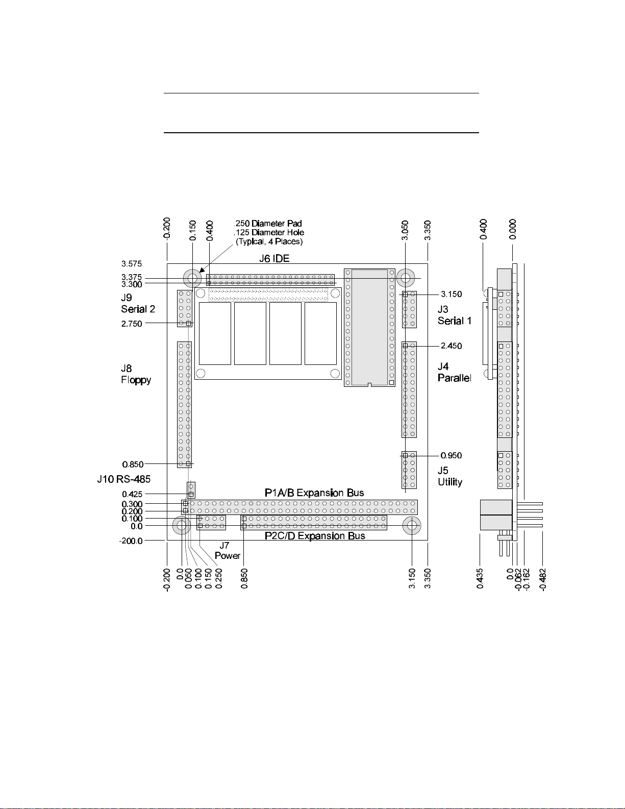
− Board Envelope: 3.6 x 3.8 x 0.92 inches (90.2 x 95.9 x 23.4 mm.). Refer to Figure 1–1 for
mounting dimensions.
− Board-to-board spacing: 0.6 inches (15.2 mm.)
n Provision for system expansion with one or more Ampro MiniModule products or other PC/104
expansion modules.
n Power requirements (typical, with 4M bytes DRAM installed):
− 25 MHz configuration: 450MA at +5V ±5%
− Standby power mode: 240MA at +5V ±5%
n Operating environment:
− Standard: 0° to 70° C (with adequate airflow)
− Extended temperature range can be tested by special order. Contact Ampro for details.
− 5% to 95% relative humidity (non-condensing)
n Storage temperature: -55° to +85° C
n Weight:
– 3.4 Oz. (95 gm)
n PC/104 expansion bus
− Stackthrough 16-bit bus connectors, for expansion via PC/104 Version 2 "double-stackthrough"
(DST) modules
− Four mounting holes
n 6-layer PCB using latest surface mount technology
1–8
Page 18
Note
Contact Ampro regarding custom configurations and special order
options.
Introduction
Figure 1–1. Mechanical Dimensions
1–9
Page 19
CoreModule/3SXi Technical Manual
1–10
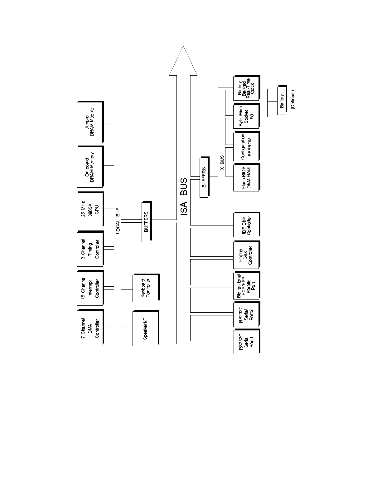
Figure 1–2. Block Diagram
Page 20

CHAPTER 2
CONFIGURATION AND INSTALLATION
2.1 INTRODUCTION
This chapter covers configuration and installation of the CoreMod ule/3SXi CPU. It includes the board’s
connector signals and pinouts, external device requirements, interconnection cable wiring, and jumper
configuration optio ns.
The topics covered in this chapter are:
n Power Connector
n DRAM me mo r y
n RS-232C/RS-485 serial ports
n Enhanced parallel port
n Floppy disk interface
n IDE hard disk interface
n 32-pin byte-wide socket
n OEM F l as h memo r y
n Utility connector (Keyboard, PC speaker, reset button, external battery)
n Watchdog timer
n Battery-backed clock
n PC/104-compatible expansion bus
2.1.1 Interface Connector Summary
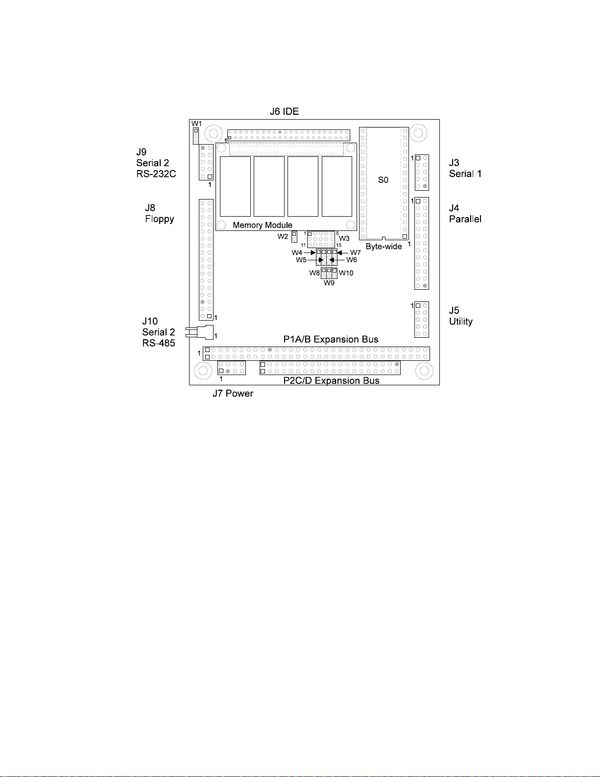
Refer to Figure 2–1 for the locations of the connectors (P1, P2, J3 - J10) and configuration jumpers
(W1 - W9).
Table 2–1 summarizes the use of the I/O connectors and Table 2–2 summarizes use of the configuration
jumpers.
Each interface is described in its own section, showing connector pinouts, signal definitions, required
mating connectors, and c onfiguratio n jumper optio ns.
Many of the connectors have a key pin removed. This allows you to block the corresponding cable
connector socket to help prevent improper assembly. Table 2–1 indicates which pins are key pins, and
Figure 2–1 shows their locations.
2–1
Page 21

CoreModule/3SXi Technica l Manua l
Table 2–1. Connector Usage Summary
Connector Function Size Key Pin
P1A/B PC/104 Expansion Bus 64-Pin B10
P2C/D PC/104 Expansion Bus 40-pin C19
J3 Serial 1 10-pin 10
J4 Parallel Port 26-pin 26
J5 Utility/Keyboard 10-pin None
J6 IDE Hard Disk Interface 44-pin
2 mm
Power, +5V; +12V,
J7
J8 Floppy Disk Interface 34-pin 6
J9 Serial 2, RS-232C 10-pin 10
J10 Serial 2, RS-485 2-pin None
Connectors
Most of the I/O connectors are dual-row headers for use with insulation displacement connectors (IDC)
and flat ribbon cable. J5 is usually implemented with discrete wires rather than flat ribbon cable. J10 is a
2-pin connector for an RS-485 twisted-pair cable.
A number of the connectors have “key pins”. Install a blocking key in the corresponding connector socket
on the mating ribbon cable to prevent misalignment.
You can design a PC board assembly, made with female connectors in the same relative positions as the
CoreModule’s connectors, to eliminate cables, meet packaging requirements, add EMI filtering, or
customize your installation in other ways.
The PC/104-compatible expansion bus appears on two connectors (P1 and P2). You can expand the
system with Ampro MiniModule products or other PC/104-compliant expansion modules. These modules
stack directly on the P1 and P2 connectors, or you can use conventional or custom expansion hardware,
including solutions available from Ampro. Contact your Ampro sales representative for information about
alternatives offered by Ampro.
-12V, and -5V to
PC/104 Bus
8-pin None
20
2–2
Page 22
Configuration and Installation
(Key pins on connectors are shaded.)
Figure 2–1. Connector and Jumper Locations
2.1.2 Jumper Configuration Options
Ampro installs option jumpers in default positions so that in most cases the CoreModule/3SXi CPU
requires no special jumpering for standard operation. You can connect the power and peripherals and
operate it immediately. The only jumpers of concern are those that configure the byte-wide socket for the
device you install.
Jumper-pin arrays are designated W1, W2 and so forth. Jumper pins are spaced 2 mm apart. A square
solder pad identifies pin 1 of each jumper array. Table 2–2 is a summary of jumper use. In the Default
column, two numbers separated by a slash (for example, 1/2) means that pins 1 and 2 are shorted with a
2 mm jumper block.
2–3
Page 23

CoreModule/3SXi Technica l Manua l
Table 2–2. Configuration Jumper Summary
Jumper
Group Function Default Description
W1 RS-232C/RS- 485 Select 1/2 1/2=RS-232C; 2/3=RS-485
W2 BIO S/OEM Flash progr am m ing
power enable
W3 Byte-Wide Socket Configuration See “Jumpering the Byte-
W4 Watchdog Timer Output
Selection
W5 DMA ACK1/ACK3 Off Parallel port DMA ACK
W6 DMA REQ 1/REQ3 Off Parallel port DMA REQ
W7 Byte-Wide Backup Power Select 1/2 (1/2) enables external
W8 Byte-W ide Battery
Backup Power
W9 BIO S/Byte-W ide Swap On Off enables access of a
W10 RS-485 Termination Off On for 100 ohm term inator
2.2 DC POWER
Off Vpp for Flash EPROM
programming
Wide Sock et” in Chapter 2
Off See “Watchdog T im er” on
Page 2–27.
select
select
battery backup for S0
Off On enables backup for S0
system BIOS from S0.
To power the module and to supply power to the PC/104 expansion bus, connect the voltages you need for
your system to J7. Refer to Table 2–3 for power connections and Table 2–4 for mating connector
information.
Table 2–3. J7 Power Connector
Pin Connection
1, 7 Ground
2, 8 +5VDC
4 +12VDC
5-5VDC
6 -12VDC
2–4
Page 24

Configuration and Installation
Table 2–4. J7 Mating Connectors
Connector Type Mating Connector
Discrete W ire, 8-pin MOLEX Housing 22-55- 2081
Pin 16-02-0103
2.2.1 Power Requirements
The CoreModule/3SXi CPU requires only +5VDC (±5%) for operation. The ±9 volts for the RS-232 ports
is generated onboard from the +5VDC supply.
The module is equipped with a +5 volt to +12 volt voltage co nverter circuit for programming 12 volt
Flash EPROMs. The supply is switched electronically, controlled by the FLASHWRI program (supplied
with the CoreModule/3SXi CPU Development Kit). Note that this supply is not intended to supply
12 volts to peripherals, and is not connected to the 12 volt input pin on the power connector or on the
PC/104 connector. There may be a requirement for an external +12 volt supply, depending on what
peripherals you connect to the CoreModule system.
The exact power requirement of the CoreModule/3SXi CPU system depends on several factors, including
the quantity of DRAM, installed byte-wide memory device, the peripheral connections, and which, if any,
MiniModule products or other expansion boards are attached to the PC/104 bus. For example, AT
keyboards draw their power from the board, and there can be some loading from the serial and parallel
ports. Consult the specifications in Chapter 1 for the basic power requirements of your model.
If you use a switching power supply, be sure it regulates properly with the load your system draws. Some
switching power supplies do not regulate properly unless they are loaded to some minimum value. If this
is the case with your supply, consult the manufacturer about additional loading, or use another supply or
another type of power source (such as a linear supply, batteries, etc.).
2.2.2 CPU Speed
The CPU speed is fixed at 25MHz. There is no user adjustment.
2.2.3 Backup Battery
You can add an external 3.6 volt lithium battery to the Utility Connector, J5, to power the onboard realtime clock and to back up an SRAM installed in the byte-wide socket. Connect the positive terminal to
J5-9 and the negative terminal to J5-1.
Here is the formula for calculating battery life (in hours):
Battery life = (battery mA-hour specification
The real-time clock battery drain is approximately 1 uA. To calculate battery life, divide the battery rating
by the sum of the clock current and the SRAM current. Then, multiply that result by the duty cycle of the
battery. That is, estimate the percentage of time the battery supplies power (while the system is off).
÷ (1 uA + SRAM backup current)) × Duty Cycle
2–5
Page 25

CoreModule/3SXi Technica l Manua l
2.3 DRAM
Standard boards have 2M or 4M b ytes of DRAM installed on the board. There is also a po sition for an
Ampro custom memory module which currently allows adding 4M bytes of additional DRAM. Contact
your Ampro sales representative for the latest information about Ampro’s custom memory modules.
When the system boots, the BIOS measures the amount of memory installed and configures the internal
memory controller for that amount. ( No j umpering or manual configura tion is re quired .) T he amount o f
memory the BIOS measured can be displayed b y running SETUP . Saving SE TUP automatically store s this
figure in the Configuration Me mory.
Note
If you change the amount of memory installed, you must run
SETUP again to save the new value in the Configuration Memory.
Onboard memory is allocated as follows (standard for the PC architecture):
n The first 640K bytes of DRAM are assigned to the DOS region 00000h to 9FFFFh.
n DRAM in the top 384K bytes of the first 1M byte is not available for user programs. DRAM is
mapped into the top 64K to shadow the ROM BIOS. DRAM can also be mapped into a portion of
this region to shadow a video BIOS (a SETUP option). (Shadowing is described in the following
section.)
n The remaining memory is mapped to extended memory starting at the 1M byte boundary.
2.3.1 Shadowing
One way to improve system performance is to “shadow” the ROM BIOS and video BIOS. When the
system operates directly from ROM code, it accesses an 8-bit memory device. When the ROM contents
are shadowed, the contents are copied into system DRAM where they are accessed as 16-bit wide data.
Shadowing a BIOS ROM substantially enhances system performance, especially when an application or
operating system repeatedly accesses the ROM. ROM BIOS shadowing is built into the Ampro Extended
BIOS. There is no user setting. Shadowing the video BIOS is a SET UP op tion. For information about
how to set the video BIOS shadowing option, refer to the SETUP section in Chapter 3.
2.3.2 Expanded Memory and Extended Memory
Memory above the 1 megabyte boundary is called “extended” memory. It is a contiguous linear block of
memor y. S o me p r og r a ms r e q ui r e th at me mo r y b e a v ai l a bl e a s “ ex p a nd e d ” ( o r “E M S ” ) me mo r y, whi c h
makes memory available as pages rather than as a contiguous block. The exact manner for accessing
expanded memory is defined in the EMS LIM 4.0 specification.
You can convert the board’s extended memory into expanded memory using DOS EMS emulation
utilities. Current versions of DOS provide EMS emulation utilities (such as EMM386) that conform to the
LIM 4.0 specification. Refer to your DOS technical documentation for instructions for using their EMS
emulation utility.
2–6
Page 26

Configuration and Installation
2.4 MATH COPROCESSOR
The 386SX CPU does not contain a floating point math coprocessor. There are no configuration jumpers
or options for a math coprocessor.
2.5 SERIAL PORTS
The CoreModule/3SXi module provides two standard RS-232C serial ports at J3 and J9. At your option,
the second serial port can be configured as an RS-485 port.
You can use the serial ports for printers, modems, terminals, remote hosts, or other RS-232C serial
devices. Many devices, such as printers and modems, require handshaking in one or both directions.
Consult the documentation for the device (s) you use fo r infor mation abo ut handshaking, cabling, and
other interface considerations.
Use of the RS-485 option offers a low cost, easy-to-use communications and networking multidrop
interface that is ideally suited to a wide variety of embedded applications requiring low-to-medium-speed
data transfer between two or more systems.
The serial ports are based on a 16550 UART-compatible controller. This is an advanced UART that has a
16-byte FIFO buffer to impro ve thro ughput.
Both serial ports support software selectable standard baud rates up to 115.2K baud, 5-8 data bits, and 1,
1.5, or 2 stop bits. Note that the IEEE RS-232C specification limits the serial port to 19.2K baud on
cables up to 50 feet in length.
2.5.1 I/O Addresses
The serial ports appear at the standard port addresses as shown in Table 2–5. These are fixed assignments
and cannot be changed. Each serial port, however, can be independently disabled using the SETUP
function, freeing its I/O addresses for use by other devices installed on the PC/104 expansion bus. For
information about serial port configuration using SETUP, see Chapter 3 .
Table 2–5. Serial Port I/O Addresses and Interrupts
Port I/O Address Interrupt
Serial 1 3F8h - 3FFh 4
Serial 2 2F8h - 2FFh 3
2.5.2 Interrupt Assignments
As shown in Table 2–5, Interrupt 4 (IRQ4) is assigned to Serial 1 and Interrupt 3 (IRQ3) to Serial 2.
These assignments can be disabled, but they cannot be changed. When a serial port is disabled, its IRQ is
available to other peripherals installed on the PC/104 expansion bus. For information about disabling the
serial ports using SETUP, see Chapter 3.
2–7
Page 27
CoreModule/3SXi Technica l Manua l
2.5.3 ROM-BIOS Installation of the Serial Ports
Normally, the ROM BIOS supports Serial 1 as the DOS COM1 device, Serial 2 as the DOS COM2
device, and so on. If you disable a serial port, and there is no substitute serial port in the system, then the
ROM-BIOS assigns the COM designations as it finds the serial ports, starting from the primary serial port
and searching to the last one. Thus, for example, if Serial 1 is disabled, the ROM-BIOS assigns COM1 to
Serial 2 (unless another Serial 1 is discovered). The ROM BIOS scans I/O addresses for serial ports in the
following order: 3F8h, 2F8h, 3E8h, 2E8h.
2.5.4 Serial Port Connectors (J3, J9)
Serial 1 appears on connector J3 and Serial 2 appears on connector J9. Table 2–6 gives the connector
pinout and signal definitions for both ports. B oth connecto rs are wired the same.
In addition, the table indicates the pins to which each signal must be wired for compatibility with standard
DB25 and DB9 connectors. The serial port pinout is arranged so that you can use a flat ribbon cable
between the header and a standard DB9 connector. Normally PC serial ports use male “DB“ connectors.
Table 2–7 shows the manufacturer’s part numbers for ribbon cable mating connectors to J3 and J9.
Table 2–6. Serial Port Connectors (J3, J9)
Pin
1
2
3
4
5
6
7
8
9
10
Signal
Name Function In/Out
DCD
DSR
RXD
RTS
TXD
CTS
DTR
RI
GND
N/A
Table 2–7. J3 and J9 Mating Connector
Data Carrier Detect
Data Set Ready
Receive Data
Request To Send
Transmit Data
Clear to Send
Data Terminal Ready
Ring Indicator
Signal Ground
Key pin
In
In
In
Out
Out
In
Out
In
-
-
DB25
Pin
8
6
3
4
2
5
20
22
7
-
Connector Type Mating Connector
Ribbon 3M 3473-7010
DB9
Pin
1
6
2
7
3
8
4
9
5
-
2–8
Discrete W ire MOLEX Housing 22-55- 2101
Pin 16-02-0103
Page 28

Configuration and Installation
2.5.5 Configuring Serial 2 for RS-485 (J10, W1, W10)
Serial 2 provides circuitry for both an RS-232C and RS-485 interface. Using jumpers, you can configure
the port to support either interface (but not both at the same time).
The RS-232C interface appears on J9. Table 2–6 shows the pinout for J9. The RS-485 interface appears
on the two-pin connector, J10. Table 2–9 shows the pinout for J10.
Figure 2–2 shows how to set W1 to select the output interface for Serial 2.
Figure 2–2. Serial 2 Interface Selection
Note
The RS-485 and RS-232C interfaces share some circuitry. If you
configure Serial 2 for RS-485, do not connect a serial device to J9.
Similarly, if you configure Serial 2 for RS-232C, do not connect
anything to J10.
The RS-485 interface specification requires that both ends of the twisted-pair cable be terminated with
100 ohm resistors. You can terminate the RS-485 interface on J10 with a resistor provided on the
CoreModule/3SXi. To terminate the line, install a jumper on W10.
Table 2–8. RS-485 Termination u sing W10
W10 Result
On Connects a 100 ohm term ination r esistor
between J10-1 (+I/O) and ground.
Off No term ination
2–9
Page 29

CoreModule/3SXi Technica l Manua l
Table 2–9. RS-485 Serial Port 2 Connector (J10)
Table 2–10. J10 Mating Connector
Connector Type Mating Connector
Pin Signal Name
1 +I/O
2 -I/O
Discrete W ire
(Locking Connector)
For further information about the RS-485 interface, see Chapter 3, Section 3.9 Serial Ports.
MOLEX Housing 22-01-2027
Pin 08-55-0102
2.5.6 RS-485 Twisted-Pai r Cabli ng Using RJ11 Connectors
Connector J10 is used for an RS-485 twisted-pair connection. In RS-485 multidrop installations, standard
RJ11 modular telephone connector jacks are often used to attach standard twisted-pair cables between
systems.
RJ11 modular connectors have 6 available contact positions, but only 4 are populated. The 4 center
conductors are wired so that the two outside and the two inside conductors are connected together. This
eliminates any confusion about pin number ing conve ntions, as a rever sal of co nnectio ns has no effe ct. I n
addition, the lines have been chosen to minimize the possibility of circuit damage should the unit be
accidentally plugged into a standard telephone outlet. (It sets the phone line to its “offhook” state to
prevent the phone from ringing.)
The recommended wiring for a J10-to-RJ11 cable is shown in Table 2–11.
Table 2–11. J10/RJ11 Cable Wiring
J10
Pin
RJ11
Pin Signal
Standard
Wire Color
1N/C
2 2 - I/O Signal Black
1 3 + I/O Signal Red
1 4 + I/O Signal Green
2 5 - I/O Signal Yellow
6N/C
When connecting the RS-485 port into a multidrop network, the devices at the ends of the network should
be terminated with a 100 ohm resistor. Installing a jumper on W10 connects a termination resistor across
the RS-485 line on the CoreModule/3SXi.
2–10
Page 30
Configuration and Installation
2.5.7 Serial Console
Unique to Ampro is ROM BIOS support for using a serial console (keyboard and display) in place of the
conventional video controller, monitor, and keyboard. See Chapter 3 for an explanation of the serial
console option.
2.5.8 Serial Dow nloader
Also unique to Ampro is ROM BIOS support for downloading a program from a host computer via a
serial port. The downloaded program is then run as if it had been loaded from disk. See Chapter 3 for an
explanation of the serial download option.
2.6 MULTIMODE PARALLEL PORT
The CoreModule/3SXi incorporates a multimode parallel port. This port supports four modes of
operation:
n Standard PC/AT printer port (output only)
n PS/2-compatible bi-directional parallel port (SPP)
n Enhanced Parallel Port (EPP)
n Extended Capabilities Port (ECP)
See “Multimode Parallel Port” in Chapter 3 for a description of the parallel por t’s modes.
This section lists the pinout of the parallel port co nnector and d escribes how to configure it for its I/O
port and interrupt assignments, and how to assign a DMA channel to the port when operating in ECP
mode. Refer to Chapter 3 for programming information, including how to use the port for bi-directional
I/O.
2.6.1 I/O Addresses
The parallel port functions are controlled by eight I/O ports and their associated register and control
functionality. By enabling the parallel port in SETUP, you configure the parallel port as the p rimary port
(typically LPT1). You may disable the port to free the hardware resources for other peripherals.
Table 2–12 lists the parallel port addresses.
Table 2–12 Parallel Port Address Configuration
Selection I/O Address
Primary 378h - 37Fh
Disable None
For details about the parallel port I/O addresses and the d ata, status, control, EP P, and ECP port b it
definitions, refer to the Parallel Port section in Chapter 3.
2–11
Page 31
CoreModule/3SXi Technica l Manua l
2.6.2 ROM-BIOS Installation of Parallel Ports
Normally, the BIOS assigns the name LPT1 to the primary parallel port, and LPT2 to the secondary
parallel port (if present in the system), and so on. However, the BIOS scans the standard addresses for
parallel ports and if it only finds a secondary port, it assigns LPT1 to that one. The BIOS scans for
parallel ports in the following address order: 3BCh, 378h, 278h.
2.6.3 Interrupts
The parallel port can be configured to generate an interrupt request upo n a variety of conditions,
depending on the mode the port is in. (These are described in Chapter 3.) In most applications, the
interrupt is not used. The standard parallel port interrup ts are:
n Primary port IRQ7
n Secondary port IRQ5
The parallel port on the CoreModule/3SXi is assigned IRQ7 when enabled in SETUP. It cannot be
changed.
2.6.4 DMA Channels
In ECP enhancement mode, the parallel port can send and receive data under control of an on-board DMA
controller. DMA channels operate with a request/acknowledge handshake protocol between an internal
DMA controller and the parallel port logic. You can select DMA request (DRQ) and DMA Acknowledge
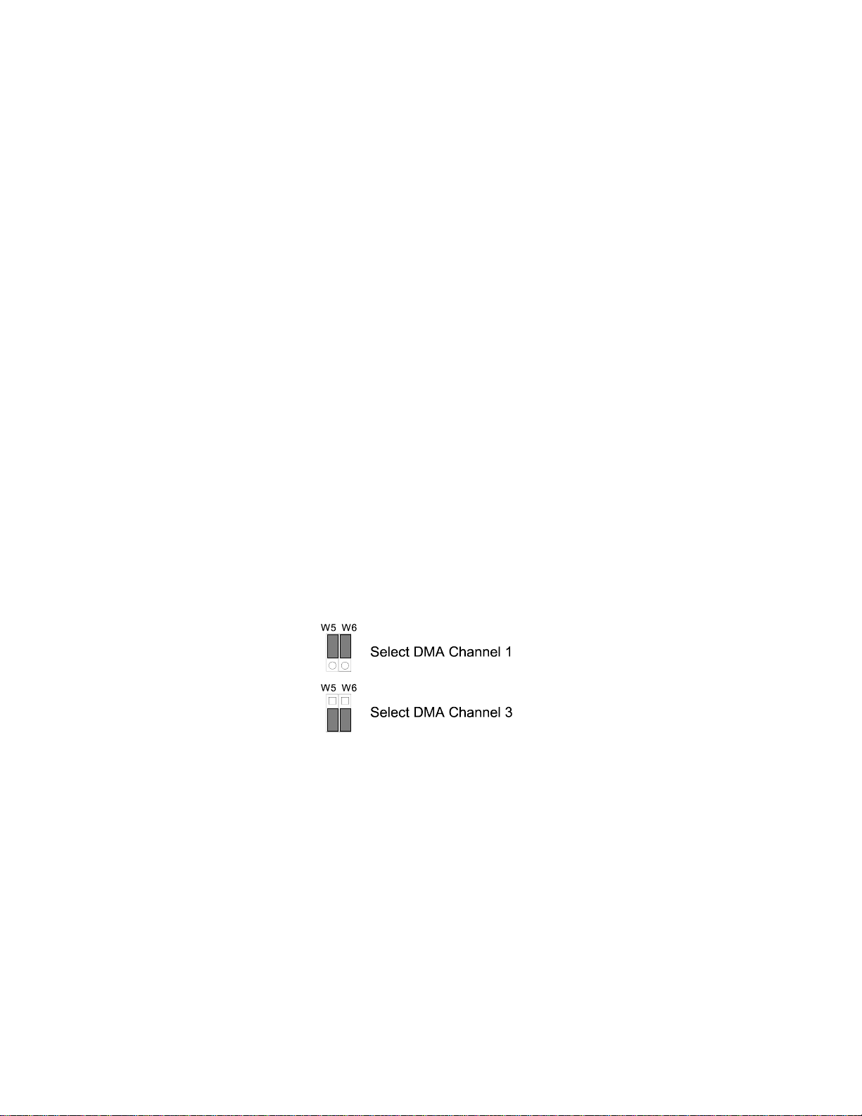
(DACK) assignments using the jumpers at W5 and W6. The parallel port may use either DMA channel 1
or DMA channel 3. T o se lect DM A channel 1 , shunt jumper W5 (1/2 ) and W 6 ( 1/2) . T o selec t DMA
channel 3, shunt jumper W5 ( 2/3) and W6 (2/3 ). See Figur e 2–3.
Figure 2–3. DMA Channel Selection (W5, W6)
If you will not be using DMA with the parallel port, leave the jumpers off. This makes the DMA controls
available to other peripherals installed on the expansion bus.
2.6.5 Parallel Port Connector (J4)
Connection to the para llel por t is through c onnecto r J4 . T able 2–13 gives this connector’s pinout and
signal definitions. You can use a flat ribbon cable between J4 and a female DB25 connector. The table
also gives the connections from the header pins to the DB25 connector. Table 2–14 gives manufacturer’s
part numbers for mating co nnect ors.
2–12
Page 32

Table 2–13. Parallel Port Connector (J4)
Configuration and Installation
J4
Pin
1
3
5
7
9
11
13
15
17
19
21
23
25
2
4
Signal
Name Function In/Out
STROBE*
Data 0
Data 1
Data 2
Data 3
Data 4
Data 5
Data 6
Data 7
ACK*
BUSY
PAPER OUT
SEL OUT
AUTOFD*
ERROR
Output data strobe
LSB of printer data
MSB of printer data
Character accepted
Cannot receive data
Out of paper
Printer selected
Autofeed
Printer error
OUT
I/O
I/O
I/O
I/O
I/O
I/O
I/O
I/O
IN
IN
IN
IN
OUT
IN
DB25
Pin
1
2
3
4
5
6
7
8
9
10
11
12
13
14
15
6
8
26
10,12,
14,16
18,20
22,24
Data lines: 24 mA sink (.4 V m ax .), 12 m A sour ce (2.4 V m in.) .
Control lines: 24 mA sink ( .4 V m ax.), open c ollector with 4.7K pull-
ups.
INIT*
SEL IN
N/A
GROUND Signal ground N/A 18-25
Initialize printer
Selects printer
Key pin
OUT
OUT
16
17
2–13
Page 33

CoreModule/3SXi Technica l Manua l
Table 2–14. J4 Mating Connector
Connector Type Mating Connector
RIBBON 3M 3399-7600
DISCRETE W IRE MOLEX HOUSING 22-55-2262
PIN 16-02-0103
Note
For maximum reliability, keep the cable between the board and the
device it drives to 10 feet or less in length.
2.6.6 IEEE-1284-Compliant Cables
Using the parallel port for high-speed data transfer in ECP/EPP modes requires special cabling for
maximum reliability.
Some of the parameters for a compliant IEEE-1284 cable assembly include:
•
All signals are twisted pair with a signal and ground return
•
Each signal and ground return should have a characteristic unbalanced impedance of 62 +/- 6 ohms
within a frequency band of 4 to 16 MHz
•
The wire-to-wire crosstalk should be no greater than 10%
Please refer to the IEEE-1284 standard for the complete list of requirements for a compliant cable
assembly, including recommended connectors. For information about the IEEE-1284 standard, see
Enhanced Parallel Port in Chapter 3.
Latch Up Protection
The parallel port incorporates chip p rotection circuitry on some inputs, designed to minimize the
possibility of CMOS “latch up” due to a printer or other peripheral being powered up while the
CoreModule/3SXi is turned off.
2.7 FLOPPY DISK INTERFACE
The onboard floppy disk controller and ROM BIOS support one or two floppy disk drives in any of the
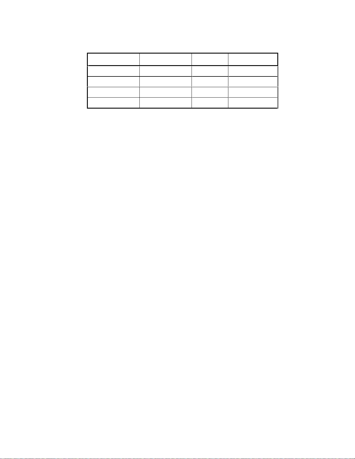
standard DOS formats shown in Table 2–15
2–14
Page 34
Configuration and Installation
Table 2–15. Supported Floppy Formats
Capacity Drive Size Tracks Data Rate
360K 5-1/4 inch 40 250 KHz
1.2M 5-1/4 inch 80 500 KHz
720K 3-1/2 inch 80 250 KHz
1.44M 3-1/2 inch 80 500 KHz
2.7.1 Floppy Drive Considerations
Nearly any type of soft-sectored, single or double-sided, 40 or 80 track, 5-1/4 inch or 3-1/2 inch floppy
disk drive is usable with this interface. Using higher quality drives improves system reliability. Here are
some considerations about the selection, configuration, and connection of floppy drives to the
CoreModule/3SXi CPU .
n Drive Interface—The drives must be compatible with the board’s floppy disk connector signal
interface, as described below. Ampro recommends any standard PC-or AT-compatible 5-1/4 inch or
3-1/2 inch floppy drive.
n Drive Quality—Use high quality, DC servo, direct drive motor floppy disk drives.
n Drive Select Jumpering—Jumper both drives for the second drive select (standard on PC drives).
n Floppy Cable—For systems with two drives, use a floppy cable with conductors 10-16 twisted
between the two drives. This is standard practice for PC-compatible systems.
n Drive Termination—Resistive terminations should be installed only on the drive connected to the
last interface cable connector (farthest from the board). Near-end cable termination is provided on the
CoreModule/3SXi CPU.
n Head Load Jumpering—When using drives with a Head Load option, jumper the drive for head load
with motor on rather than head load with drive select. This is the default for PC-compatible drives.
n Drive Mounting—If you mount a floppy drive very close to the Little Board or another source of
EMI, you may need to place a thin metal shield between the disk drive and the device to reduce the
possibility of electromagnetic interference.
2.7.2 Floppy Interface Configuration
The floppy interface is configured using SETUP to set the number and type of floppy drives connected to
the system. Refer to the SETUP section in Chapter 3 for details.
If you don’t use the floppy interface, disable it in SETUP. This frees its I/O addresses (3F0h - 3F7h),
DMA2, and IRQ6 for use by other peripherals installed on the PC/104 bus.
2.7.3 Floppy Interface Connector (J8)
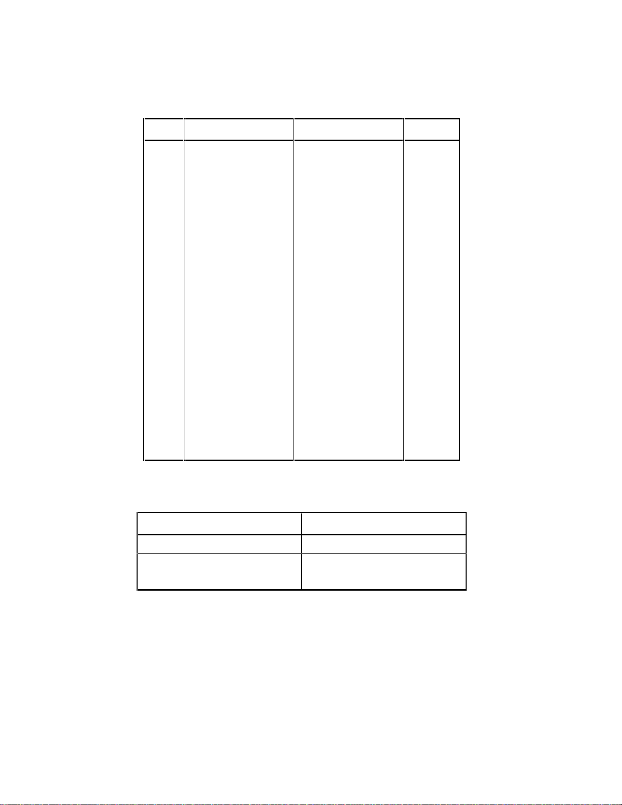
Table 2–16 shows the pinout and signal definitions of the floppy disk interface connector, J8. The pinout
of J8 meets the AT standard for floppy drive cables. Table 2–17 shows the manufacturer’s part numbers
for mating connector s.
2–15
Page 35
CoreModule/3SXi Technica l Manua l
Table 2–16. Floppy Disk Interface Connector (J8)
Pin Signal Name Function In/Out
2
4
6
8
10
12
14
16
18
20
22
24
26
28
30
32
34
RPM/-RWC
N/A
N/A
-IDX
-MO1
-DS2
-DS1
-MO2
-DIRC
-STEP
-WD
-WE
-TRKO
-WP
-RDD
-HS
-DCHG
Speed/Precomp
(Not used)
Key pin
Index Pulse
Motor On 1
Drive Select 2
Drive Select 1
Motor On 2
Direction Select
Step
Write Data
Write Enable
Track 0
Write Pr otect
Read Data
Head Select
Disk Change
OUT
N/A
N/A
IN
OUT
OUT
OUT
OUT
OUT
OUT
OUT
OUT
IN
IN
IN
OUT
IN
1-33
(all odd)
Table 2–17. J8 Mating Connector
Signal grounds
N/A
Connector Type Mating Connector
Ribbon 3M 3414-7600
Discrete W ire MOLEX Housing 22-55-2342
Pin 16-02-0103
2.8 IDE HARD DISK INTERFACE
The CoreModule/3SXi CPU provides an interface for one or two Integrated Device Electronics (IDE)
hard disk drives. IDE drives, the most popular and cost-effective type of hard drive currently available,
have an internal hard disk controller. There are also many CD-ROM drives designed to use the IDE
interface. If you attach a CD-ROM drive to the IDE port, you will need a driver (supplied by the CDROM drive manufacturer or your operating system) to access the device .
2–16
Page 36

Configuration and Installation
2.8.1 IDE Connector (J6)
The IDE interface appears at connector J6, a 44-pin, dual-row 2 mm. right-angle connector. Table 2–18
shows the interface signals and pin outs for the IDE interface connector. Table 2–19 shows
manufacturer’s part numbers for mating connec tor s to J 6.
Note
For maximum reliability, keep IDE drive cables less than 18 inches
long.
Table 2–18. IDE Drive Interface Connector (J6)
Pin Signal Name Function In/Out
1 -HOST RESET Reset signal from host OUT
3 HOST D7 Data bit 7 I/O
4 HOST D8 Data bit 8 I/O
5 HOST D6 Data bit 6 I/O
6 HOST D9 Data bit 9 I/O
7 HOST D5 Data bit 5 I/O
8 HOST D10 Data bit 10 I/O
9 HOST D4 Data bit 4 I/O
10 HOST D11 Data bit 11 I/O
11 HOST D3 Data bit 3 I/O
12 HOST D12 Data bit 12 I/O
13 HOST D2 Data bit 2 I/O
14 HOST D13 Data bit 13 I/O
15 HOST D1 Data bit 1 I/O
16 HOST D14 Data bit 14 I/O
17 HOST D0 Data bit 0 I/O
18 HOST D15 Data bit 15 I/O
20 KEY Keyed pin N/C
21 RSVD Reserved N/C
23 -HOST IOW Write strobe OUT
25 -HOST IOR Read s trobe OUT
27 RSVD Reserved N/C
28 RSVD Reserved N/C
29 RSVD Reserved N/C
31 HOST IRQ14 Drive inter rupt request IN
2–17
Page 37
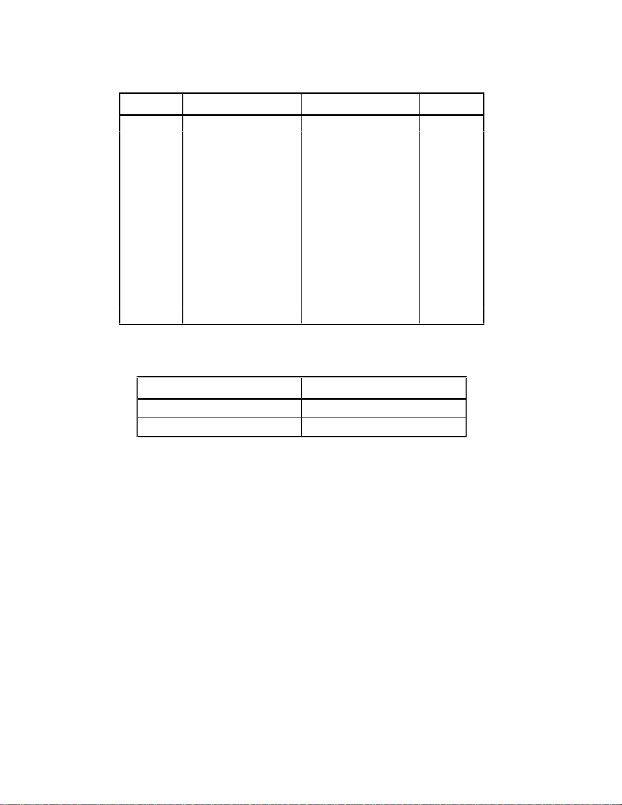
CoreModule/3SXi Technica l Manua l
Table 2–15. IDE Drive Interface Connector (J6) (cont.)
Pin Signal Name Function In/Out
32 RSVD Reserved N/C
33 HOST A1 Drive address 1 OUT
34 RSVD Reserved N/C
35 HOST AD0 Drive address 0 OUT
36 HOST AD2 Drive address 2 OUT
37 -HOST CS0 Chip select OUT
38 -HOST CS1 Chip select OUT
39 -HOST SLV/ACT Drive active/drive
41, 42 +5V Power OUT
2, 19, 22,
24, 26, 30,
40, 43
21, 28, 29 N/C No Connection -
10K Pull-
slave
GND Ground OUT
up
Table 2–19. J6 Mating Connector
Connector Type Mating Connector
Ribbon Cable, 1 mm. 44 cond. 3M 3625/44
Ribbon Cable Connector ASTRON AT-IDCSK-44-11- GF
2.8.2 IDE Cable Adapter
Many IDE hard dr ives and CD-ROM d rives have 40 -pin c onnect ors with .1 inc h pin sp acing. Ampro
makes an adapter board that you can install on your drive to convert it from the larger 40-pin format to the
44-pin 2 mm. format to make it compatible with the 2 mm. cable defined by the components listed in
Table 2–19. For details, ask your Ampro sales representative about the IDE Cable Adapter.
2.8.3 IDE Interface Configuration
Use SETUP to specify your IDE hard disk drive type. Refer to the SETUP section in Chapter 3 for
details.
If you do not find a drive type whose displayed parameters match the drive you are using, use drive type
48 or 49. These allow you to manually enter the drive’s parameters. The drive manufacturer provides the
drive parameters—check the drive’s documentation for the proper values to enter.
If you are using a newer IDE drive, use drive type AUTO. It automatically configures the drive type
parameters from information provided by the drive itself. The Autoconfigure function is described in
Chapter 3.
If you use an IDE drive in your system, you can still add SCSI drives or other SCSI peripherals. The
Ampro ROM BIOS provides a means for allowing both IDE and SCSI drives on the same system. See the
SETUP description in Chapter 3 for details.
2–18
Page 38

Configuration and Installation
2.9 BYTE-WIDE SOCKET
The CoreModule/3SXi CPU has a 32-pin onboard byte-wide memory socket, designated S0. This socket
can accept a wide variety of EPROM, Flash EPROM, SRAM, and nonvolatile RAM (NOVRAM) devices.
Battery backup power can be connected to S0 using a jumper option to make a standard SRAM “nonvolatile” (retains data while system power is off).
You can use a memory device installed in the byte-wide socket for a variety of purposes:
n Simple program storage
n BIOS extension
n Solid State Disk (SSD) drive
Table 2–20 shows representative byte-wide memory devices that can be installed in the byte-wide socket.
The table gives examples of generic part numbers, the size of the device (K bytes), and the DIP package
pin count. It also lists the SSD device type, used by the Ampro Solid State Disk (SSD) Support Software
to identify memory devices.
Table 2–20. Typical Byte-wide Devices
SSD Device
Type Size
Package
Pins
Generic
Part Number
EPROMs
EPROM32 32K byte 28 27C256
EPROM64 64K byte 28 27C512
EPROM128 128K byte 32 27C010
EPROM256 256K byte 32 27C020
EPROM512 512K byte 32 27C040
EPROM1024 1024K byte 32 27C080
Flash EPROMs
EPROM128 128K bytes 32 28F010
EPROM256 256K bytes 32 28F020
EPROM512 512K bytes 32 29F040
2–19
Page 39
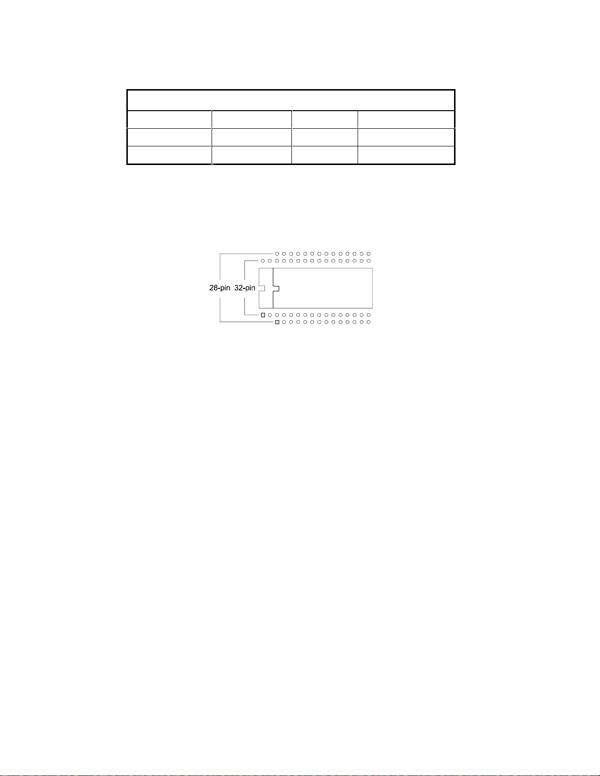
CoreModule/3SXi Technica l Manua l
Table 2–21. Typical Byte-wide Devices (Cont.)
SRAMs
SRAM32 32K bytes 28 43256
SRAM128 128K bytes 32 62204
SRAM512 512K bytes 32 434000
The pinout of the 32-pin socket can be configured to comply with both the 28-pin and 32-pin JEDEC
standards. You can install a 28-pin device in the 32-pin socket. Install the 28-pin device with pin 1
oriented to the socket’s pin 3, as indicated in Figure 2–4.
Figure 2–4. Using 28- and 32- pin Devices in 32-pin Sockets
2.9.1 Addressing the Byte-wide Socket
Use SETUP to specify the size and starting address of the byte-wide socket, and whether the BIOS
enables the socket upon system initialization.
Table 2–22 lists the possible settings for sizes and address ranges of the byte-wide socket.
2–20
Page 40

Configuration and Installation
Note
When the byte-wide socket is enabled, the memory address space it
uses is unavailable for other devices, even if no memory device is
installed in the socket. You must disable the byte-wide socket in
SETUP before you can use the memory space for other purposes.
Table 2–22. Window Size and Address Selection
Window Address
DISABLE N/A
64K D0000-DFFFFh
64K E0000-EFFFFh
128K D0000-EFFFFh
The size of the device installed in the byte-wide socket is not limited to 128K bytes. Using a page
addressing scheme, devices (or modules) up to 1M bytes can be used. Higher address lines (A16-A19)
are synthesized and can be set by software using Ampro extended BIOS function calls. A description and
examples of byte-wide page control are provided in Chapter 3.
If devices larger than 64K bytes are installed, you must select which page is visible in the address
window. A page is 64K bytes. (If the size is set to 128K bytes, a single 128K byte window is established.
Paging is only available with the 64K window setting.) The Ampro Extended BIOS provides convenient
software calls to manage enabling/disabling the socket and selecting pages. Refer to Chapter 3 for details
about the byte-wide extended ROM-BIOS calls.
If you install a device that is smaller than the selected window size, the contents of the device are
duplicated in the byte-wide socket’s memory space. For example, the software will see two copies of a
32K device in a 64K window, and 4 copies in a 128K window.
ROM-BIOS Extensions
The system can be configured to run its application from the byte-wide socket instead of loading it into
DRAM from a disk drive. This technique, known as a ROM BIOS extension, directly executes the
application during the Power On Self Test (POST) instead of booting from floppy or hard disk. The
ROM-BIOS extension concept, and its practical implementation, is discussed in Ampro Application Notes
AAN-8702 and AAN-9003.
Performance Issues
Note that executing programs directly from the byte-wide socket can adversely affect system performance.
There are a number of factors that can contribute to the performance impact:
n The byte-wide device is substantially slower than DRAM, as it is an 8-bit device instead of 16-bit.
n The device is accessed from the PC expansion bus which is much slower than the high-speed
processor memory bus.
You can improve performance substantially by copying the contents of the byte-wide device into RAM
and executing the RAM copy.
2–21
Page 41

CoreModule/3SXi Technica l Manua l
2.9.2 OEM Flash Memory
Access to the byte-wide socket is integrated with access to an onboard Flash memory device, designated
the OEM Flash Memory in SETUP. The OEM Flash memory acts as a second byte-wide device, in that
you access it through the same code mechanisms as the byte-wide socket. These mechanisms are described
in Chapter 3. (There are no jumpers to configure the OEM Flash memory.)
Only one of the two devices can be enabled at a time. When you enable the OEM Flash memory (using an
extended BIOS call), the byte-wide is automatically disabled, and vice-versa.
The first 64K bytes of the Flash memory device hold the ROM BIOS. The remaining portion can be used
by OEMs or end-users in a manner similar to the byte-wide socket. In the standard version of the
CoreModule/3SXi, the remaining portion is 64K bytes (the second 64K portion of a 128K device). By
special order, you can substitute a 1M byte Flash device. As with the 128K device, the first 64K is used
for the ROM BIOS. The remaining area is available for the embedded system. (Contact your Ampro Sales
Representative for details about ordering the larger memory size.)
Set the address parameters for both the byte-wide socket and the OEM Flash device with SETUP. Refer to
Chapter 3 for details.
2.9.3 Solid State Disk (SSD) Drives
Using the Ampro Solid State Disk (SSD) Support Software, you can configure an EPROM, Flash
EPROM, or SRAM solid-state device, installed in the byte-wide socket, or the OEM Flash device, to act
as a solid-state floppy disk drive.
No custom programming is required. Regular DOS-compliant programs, including standard DOS utilities,
can be used without modification. Ampro’s SSD support software creates data image files, based on your
application programs and operating system, which are programmed into the device you install in the bytewide socket. The Ampro ROM-BIOS treats the device like one or more disk drives, loading the programs
into DRAM for execution. You can use SSD drives in addition to, or instead of, normal floppy and hard
disk drives. You can increase the system SSD capacity by adding one or more of Ampro’s SSD expansion
modules.
If your board is equipped with the optional 1M b yte OEM Flash device, you can install the TrueFFS Flash
file system in it. This creates a fully read/write-capable solid state disk without adding any additional
components to your system. Instructions on how to configure the OEM Flash device with TrueFFS Flash
file system is in the TrueFFS manual that comes with the software.
2.9.4 Jumpering the Byte-Wide Socket
You must jumper the byte-wide socket for the device you install. Jumper array W3 configures S0 for a
particular device type.
Table 2–23 shows how to install jumpers for a variety of supported EPROM memory devices.
Table 2–24 shows how to install jumpers for a variety of supported Flash EPROM memory devices.
Table 2–25 shows how to install jumpers for a variety of supported SRAM and NOVRAM memory
devices.
2–22
Page 42
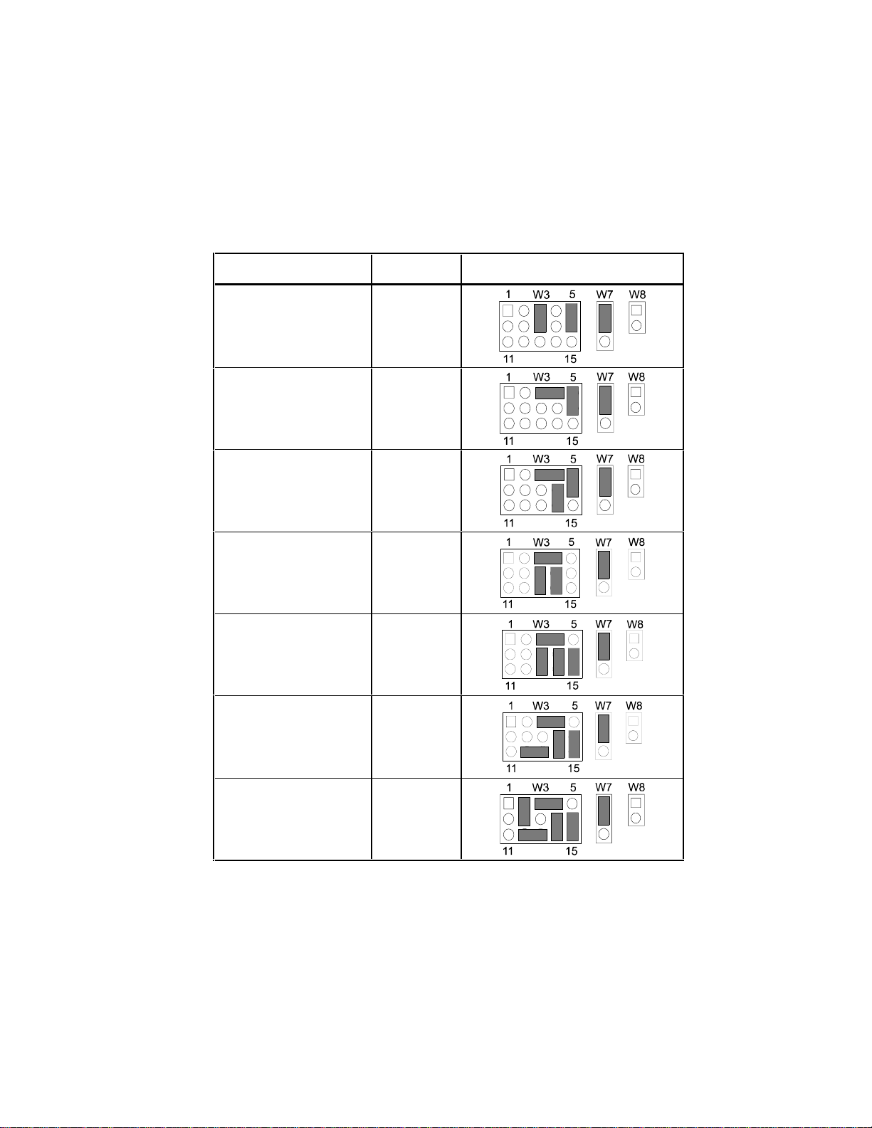
Configuration and Installation
2.9.5 Using EPROMs
Table 2–23 shows the jumpering for supported EPROM devices. If you install an EPROM, make sure the
jumper on W8 is removed and the jumper on W7 is on pins 1/2 to prevent premature discharge of the
onboard ba ckup b attery. Some EP ROMs d raw current thr ough their chip se lect lines ( or o ther p ins) when
powered down.
Table 2–23. EPROM Jump ering fo r S0
EPROM Pins Jumper Diagram
8K EPROM 27C64
16K EPROM 27C128
8K EEPROM 28C64
32K EPROM
27C256
64K EPROM
27C512
128K EPROM
27C010
256K EPROM
27C020
512K EPROM
27C040
28
28
28
32
32
32
1M EPROM 27C080 32
2–23
Page 43
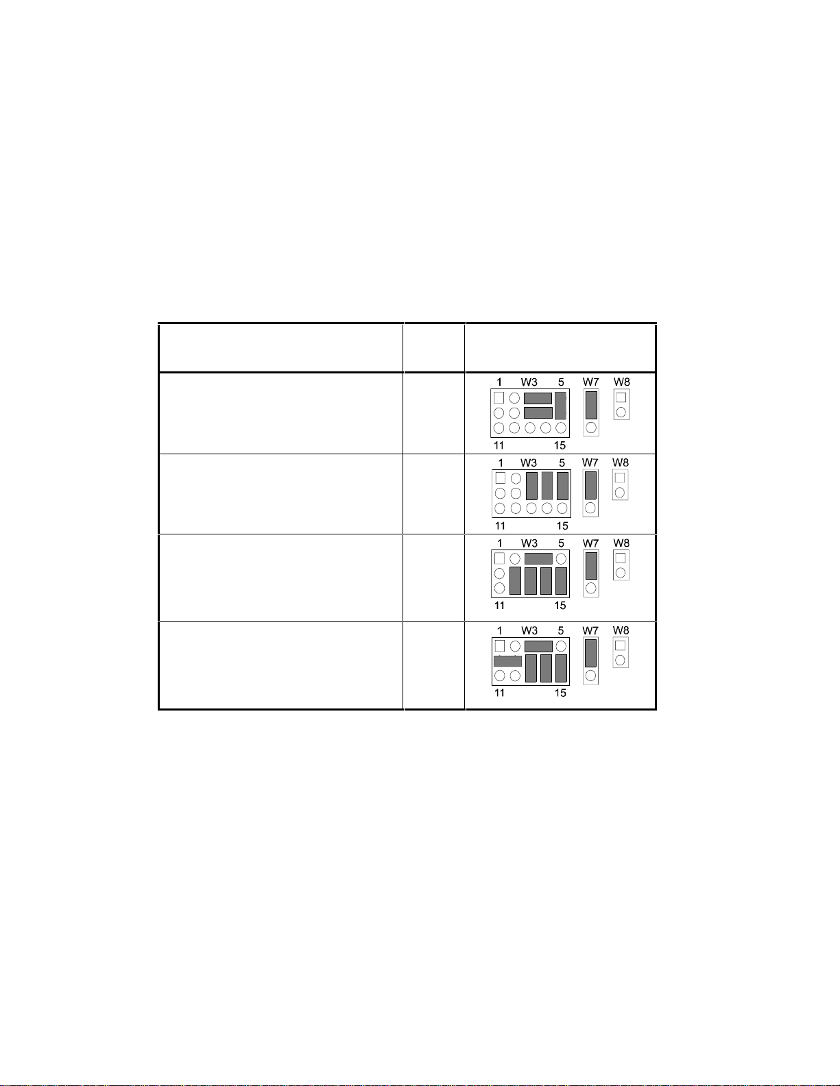
CoreModule/3SXi Technica l Manua l
2.9.6 Using Flash EPROMs
Flash programming power for +12V Flash devices is provided by an onboard power supply. You do not
need to connect an external +12V power supply to program Flash devices. Programming power is
switched under software control so that it is applied only during the actual programming process (to
prevent accidental corruption of the data). A utility for programming supported Flash devices is included
on the utility disk that is provided with the CoreModule/3SXi CPU Development Kit.
If you install a Flash EPROM, make sure the jumper on W8 is removed and the jumper on W7 is on pins
1/2 to prevent premature discharge of the onboard backup battery. Some Flash EPROMs draw current
through their chip selec t lines (o r othe r pins) when powered d own.
Table 2–24. Flash EPROM Jumpering for S0
Flash EPROM
Typical Devices Pins Jumper Diagram
32K 5V Flash EPROM 29C256 28
32K 5V Flash EPROM 28C256 28
64K 5V Flash EPROM 29F512
128K 5V Flash EPROM 29F010
256K 5V Flash EPROM 29F020
512K 5V Flash EPROM 29F040
32K 12V Flash EPROM 28F256
64K 12V Flash EPROM 28F512
128K 12V Flash EPROM 28F010
256K 12V Flash EPROM 28F020
32
32
2–24
Page 44
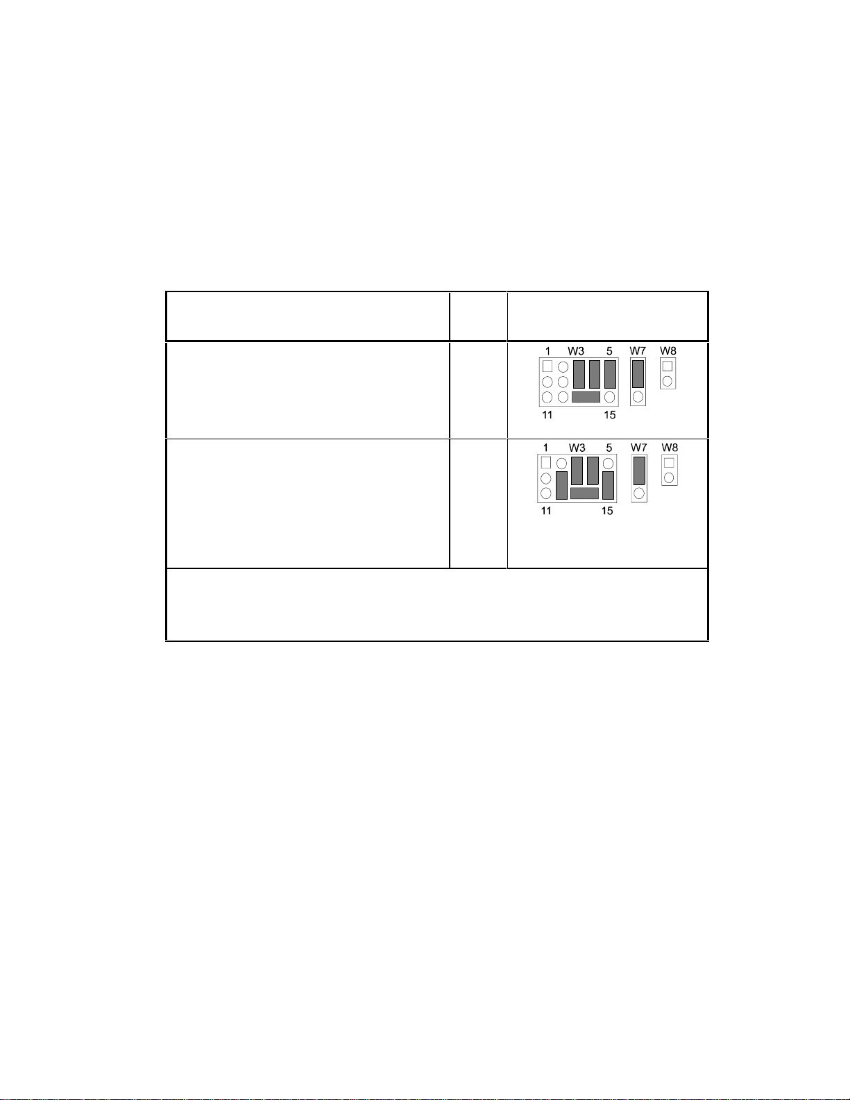
Configuration and Installation
2.9.7 Using SRAMs
If you install an SRAM, you can provide backup power from the battery when power is off by shorting
W8 and W7-2/3. If you use the SRAM for “scratchpad” storage and do not want to retain data when
power is off, remove the jumper from W8 and install a jumper on W7-1/2.
A typical 165 milliamp-hour external battery provides sufficient current for the onboard real-time clock
for a 10 year life, but if you are going to battery-back-up a device in S0, Ampro recommends a larger
battery. For calculating battery life, see page 2–5, Backup Battery.
Table 2–25. SRAM and NOVRAM Jumpering for S0
SRAM
Typical Devices Pins Jumper Diagram
32K SRAM 43256
32K NOVRAM Dallas DS1230Y
Benchmarq BQ4011Y
128K SRAM 628128
128K NOVRAM Dallas DS1245Y
Benchmarq BQ4013Y
512K SRAM 628512
512K NOVRAM Dallas DS1650Y
Benchmarq BQ4015Y
NOTE: W7 and W8 are show configured for (self-powered) NOVRAMs. To configure
W7 and W8 for SRAM battery backup, install a jumper on W8 and move the jumper on
W7 to 2/3.
28
32
2.9.8 Byte-Wide Socket Signals
W3 is used to configure the byte-wide socket for specific memory devices. In addition, jumpers W7 and
W8 control the backup battery to S0 for use with SRAMs.
Table 2–26 lists the signals that appear on the pins of W3.
2–25
Page 45

CoreModule/3SXi Technica l Manua l
Table 2–26. Byte-Wide Jumper Pin Signals (W 3)
W3 Pin Signal
Name Description
1 N/C No connec tion
2 A19 Address A19
3 Pin 29 Connection to pin 29 of the byte-wide socket
4 A14 Address SA14 from the expans ion bus
5 Vcc or
backup
battery
6 Vpp Programming power for F lash devices
7 Pin 1 Connection to pin 1 of the byte-wide socket
8 -SMEMW Write s trobe
9 Pin 3 Connection to pin 3 of the byte-wide socket
10 Pin 30 Connected to pin 30 of the byte-wide socket
11 N/C No Connection
12 A18 Address A18
13 Pin 31 Connection to pin 31 of the byte-wide socket
14 A15 Address SA15 from the expansion bus
15 A17 Address A17
W7 and W8 Options
Some EPROMs draw power thro ugh their c hip selec t lines when Vcc is off. This co uld d rain the r eal-time
clock battery if it were connected to such a device. Removing the jumper from W8 disconnects the battery
from the byte-wide circuit (leaving it connected to the real-time clock) and prevents an EPROM from
draining the battery prematurely.
Connected to the center pin of W7. W7-1 connects
to +5V. W7-3 c onnects to the bac k up battery.
Some byte-wide devices require more current than can be handled by the power switch that controls Vcc
to the byte-wide socket. The power switch is designed to switch between battery power and Vcc for an
SRAM which has very low current drain. If you are using a Flash memory or EP ROM in the b yte-wide
socket, set W7-1/2 to conne ct the memory device dir ectly to Vcc r ather than thro ugh the po wer switch
(W7-2/3).
2.10 BATTERY-BACKED CLOCK
An AT-compatible battery-backed real-time clock (with CMOS RAM) is standard on the
CoreModule/3SXi CPU. The clock can be po wered by a 3.6 volt Lithium battery connected to the Utility
Connector, J5. Battery drain for the clock is less than 1 uA.
Use the Ampro SETUP utility to set the current time and date in the real-time clock, as well as SETUP
information in the CMOS RAM portion of the clock chip (configuration memory).
2–26
Page 46

Configuration and Installation
The contents of the configuration memory are also stored in an onboard EEPROM. The ROM BIOS reads
the EEPROM to get configuration information if the CMOS RAM data is lost. This means that the board
will function without the battery. Note that without a battery, the real-time clock date and time will not be
correct.
2.11 WATCHDOG TIMER
A unique feature of the onboard clock circuitry is a watchdog timer. You can program this timer to
generate an interrupt or reset signal if the programmed time interval expires before the timer is
reinitialized. Use SETUP to select the time interval. The options are: Disable, 30 seco nds, 60 seco nds,
and 90 seconds.
The watchdog timer uses the standard alarm feature of the real-time clock. In a standard AT, the alarm
output is connected to IRQ8. On the CoreModule/3SXi CPU you can also jumper the alarm output to I/O
Channel Check (-IOCHCK) or RESET with W4. I/O Channel Check is the bus signal that triggers a nonmaskable interrupt (NMI). RESET is a hard reset signal, the same as pressing the Reset button. Watchdog
timer responses are summarized in Table 2–27.
Table 2–27. Watchdog Timer Setup
Jumper W4 SETUP WDT Response
W4-1/2 Shorted Enabled Hardware Reset
W4-2/3 Shorted Enabled I/O Channel Check (NMI)
W4 Open Enabled IRQ8 turns off interrupt. System
continues unaffected .
W4 Open Disabled No action.
Note
If you use the MS-DOS operating system, you cannot use the
watchdog timer to monitor the boot process. MS-DOS resets the
alarm clock in the real-time clock at boot time.
2.12 UTILITY CONNECTOR (J5)
Six functions appear on the 10-pin connector at J5. These are:
n PC speaker
n Push-button reset switch
n Standard PC keyboard interface
n External back-up battery for the real-time clock and byte-wide S0
2–27
Page 47

CoreModule/3SXi Technica l Manua l
Table 2–28 shows the pinout and signal definitions of the Utility Connector. Since there are connections
for diverse features on this single connector, you would usually choose a discrete-wire connector rather
than a ribbon cable connector, though this is not a requirement. Table 2–29 shows manufacturer’s part
numbers for both types of mating connectors.
Table 2–28. Utility Connector (J5)
Pin Signal Name Function
1 Speak er + PC audio signal output
2 BATV- Negative ter m inal of ex ternal back up battery
3 Reset Manual reset button.
4 N/C No connec tion
5 Keyboard Data Keyboard serial data
6 Keyboard Clock Keyboard clock
7 Ground Keyboard ground
8 Keyboard Power Keyboard +5V power
9 BATV+ Pos itive term inal of external bac kup batter y
10 N/C N o connection
Table 2–29. J5 Mating Connector
Connector Type Mating Connector
Ribbon 3M 3473-7010
Discrete W ire MOLEX Housing 22-55-2101
Pin 16-02-0103
2.12.1 Speaker Connections
The board supplies about 100 mW for a speaker on J5-1. Connect the other side of the speaker to ground
(J5-2). A transistor amplifier buffers the speaker signal. Use a small general purpose 2 or 3 inch
permanent magnet speaker with an 8 ohm voice coil. Refer to Chapter 3 for an explanation of the PC
speaker circuit architecture.
2.12.2 Push-button Reset Connection
J5-3 provides a connection for an external normally-open momentary switch to manually reset the system.
Connect the other side of the switch to ground. The reset signal is “de-bounced” on the board.
2–28
Page 48

Configuration and Installation
2.12.3 Keyboard Connections
You can connect a n AT ( not P C) ke yboard to the keyboar d p ort. J5-5 thro ugh J5 -8 pr ovide this function.
Normally, AT keyboards include a cable that terminates in a male 5-pin DIN plug for connection to an
AT. Table 2–30 gives the keyboard connector pinout and signal definitions, and includes corresponding
pin numbers of a no rmal AT D IN ke yboa rd c onne cto r.
Table 2–30. Keyboard Connector (J5)
J5 Pin Signal Name DIN Pin
5 Keyboard Clock 1
6 Keyboard Data 2
N/C No connection 3
7 Ground 4
8 Keyboard power 5
2.12.4 External Battery Connections
To connect an external battery, connect its positive terminal to J5-9 and its negative terminal to J5-2. Use
a 3.6 volt lithium cell.
The battery is connected by a low-drop Schottky diode. Two blocking devices are in series with the
battery, complying with UL recommendations for lithium batteries.
2.13 AT EXPANSION BUS
The PC/AT expansion bus appears on a pair of header connectors at P1 and P2. P1 is a 64-pin female
dual-row header. P2 is a 40 -pin female d ual-r ow header . P ins fro m both hea der s extend thr ough the b oar d,
providing male connections for PC/104-compliant peripherals or other devices.
The PC-bus subset of the expansion bus connects to the first 62 p ositions of P 1; the two additional
positions of P1 (A32 and B32) are added grounds to enhance system reliability. Connector P2 replaces the
36-pin edge card connector of a conventional ISA expansion bus. It has extra ground positions at each end
of the connector (C0, D0, D19). (C19 is a key pin.) The extra grounds C0 and D0 are numbered “0” to
keep the pin numbers of the remaining signals on the connector the same as those on the standard ISA
bus. The layout of signals on P1 and P2 is compliant with the PC/104 bus specification (IEEE P996.1
(proposed)). PC/104-compatible expansion modules can be installed on the CoreModule/3SXi CPU
expansion bus.
The buffered output signals to the expansion bus are standard T T L level signals. All inputs to the
CoreModule/3SXi CPU operate at TT L levels and present a typical CMOS load to the expansion bus. The
current ratings for most output signals driving the AT expansion bus are shown in Table 2–31 through
Table 2–34 , and indicate how the signals are terminated on the CoreModule/3SXi CPU.
2.13.1 Onboard MiniM odule Expansi on
You can install one or more Ampro MiniModule products or other PC/104 modules on the
CoreModule/3SXi CPU expansion connectors. When installed on P1 and P2, the expansion modules fit
2–29
Page 49
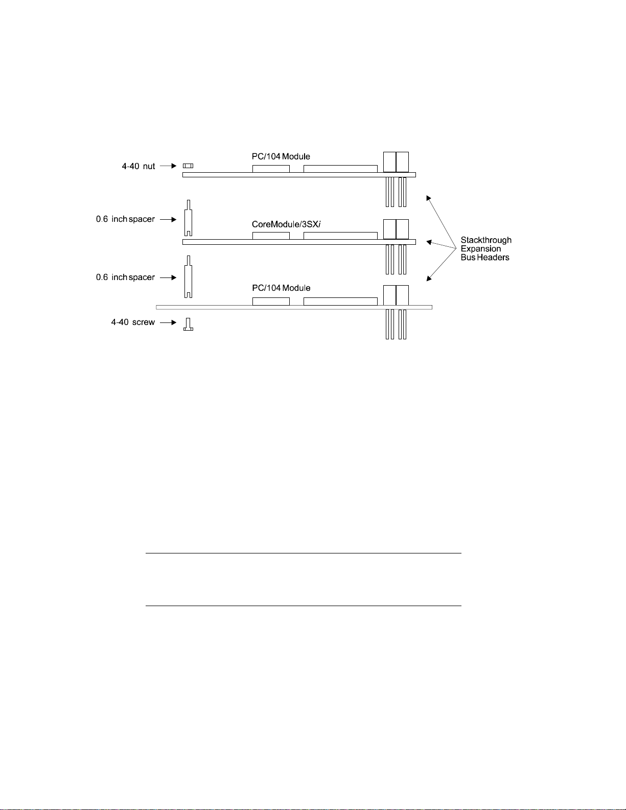
CoreModule/3SXi Technica l Manua l
within the CoreModule/3SXi CPU’s outline dimensions. Most Ampro MiniModule products have
stackthrough connectors c ompatible with the PC/104 Version 2.1 specification. You can stack several
modules on the CoreModule/3SXi CPU headers. Each additional module increases the thickness of the
package by 0.66 inches (17 mm). See Figure 2–5.
Figure 2–5. Stacking PC/104 Modul es
with the CoreM odule/3SX
i
CPU
2.13.2 Using Standard PC and AT Bus Cards
Ampro offers several options that allow you to add conventional 8-bit and 16-bit ISA expansion cards to
the CoreModule/3SXi CPU system. Contact Ampro for further information about optional bus expansion
products.
2.13.3 Bus Expansion Guidelines
Note
Ampro does not recommend the use of ribbon cables for bus
expansion in production configurations. If cables are unavoidable,
the following guidelines apply.
There are restrictions when attaching peripherals to the expansion bus with ribbon cables. If cables are
too long or improperly terminated, noise and cross-talk introduced by the ribbon cables can cause errors.
Ampro strongly recommends that you confor m to the following guideline s:
2–30
Page 50

Configuration and Installation
Cable Length and Quality—In general, keep the bus expansion cable as short as possible. Long cables
reduce system reliability.
•
Do not use cables longer than 6 inches.
•
Carefully measure signal quality on each bus line. You may need to add termination to correct signal
degradation.
Backplane Quality—If you connect a backplane to the CoreModule/3SXi CPU. be sure to use a high
quality backplane that minimizes signal crosstalk. Use a backplane that has power and ground planes
between trace layers, and run guard traces between sensitive bus signals.
Eliminating Reset and TC Noise—Many cards have asynchronous TTL logic inputs that are susceptible
to noise and crosstalk. The active high RESET and TC bus lines are especially vulnerable. You can make
these signals more reliable by adding a 200 pF to 500 pF capacitor between the signal and ground to
prevent false triggering by filtering noise on the signals. These RESET and TC filters are included on
most Ampro backplane expansion products.
Bus Termination
Some backplanes include bus termination to improve system reliability by matching backplane impedance
to the rest of the system. The IEEE-P996 draft specification for the AT expansion bus recommends the
use of AC termination (sometimes called “snubbers”) rather than resistive termination. The recommended
AC termination is a 50 to 100 pF capacitor, in series with a 50 to 100 ohm resistor, from each signal to
ground. Ampro provides positions for OEM addition o f AC termination on most bus expansion products.
These positions are designed to accommodate 9-pin 8-terminator Single Inline Package (SIP) terminators.
Here are some manufacturer part numbers for 9-pin, eight-terminator devices with 100 pF capacitors in
series with 100 ohm resistors:
n Dale CSRC-09C30-101J-101M
n Bourns 4609H-701-101/101
Caution
Do not use resistive bus termination! If the signal requires
termination, use AC termination only.
The actual requirements for signal termination depend on system configuration, interconnecting bus cable,
and on the number and type of expansion modules used. It is the system engineer’s responsibility to
determine the need for termination.
For engineering development purposes, you can expand a CoreModule/3SXi system by connecting short
ribbon cables to the header connectors. Ampro makes a small ribbon cable connector assembly, the
Double Stackthrough (DST) Cable Adapter, that you can use to connect standard ribbon cables to the
female expansion bus connectors on the CoreModule/3SXi CPU. Contact your Ampro sales representative
for more information about the DST Cable Adapter.
2–31
Page 51

CoreModule/3SXi Technica l Manua l
2.13.4 Expansion Bus Connector Pinouts
Table 2–31 through Table 2–34 show the pinout and signal functions on the PC/104-compliant expansion
bus connectors.
The CoreModule/3SXi CPU does not generate ±12VDC or -5VDC for the expansion bus. If devices on
the bus require these voltages, they can be supplied to the bus connector from the Power Connector (J7).
You do not need to add a +12V supply to program Flash EPROMs installed in the byte-wide socket, or for
the onboard Flash device. An onboard supply provides the programming voltage. However, this supply
does not provide power to the expansion bus. Most Ampro expansion products provide onboard DC-toDC converters to convert the +5V supply to other voltages they require.
The expansion bus p in numbers sho wn in the following tables co rre spond to the sche me normally used on
ISA expansion bus card sockets. Rather than numerical designations (1, 2, 3) they have alpha-numeric
designations (A1, A2…, B1, B2…, etc.)
2–32
Page 52

Configuration and Installation
Table 2–31. AT Expansion Bus Connector, A1-A32 (P1)
Signal
Pin
A1
A2
A3
A4
A5
A6
A7
A8
A9
A10
A11
A12
A13
A14
A15
A16
A17
A18
A19
A20
A21
A22
A23
A24
A25
A26
A27
A28
A29
A30
A31
A32
* PU = pull up; PD = pull down; S = resistance in series. All values in ohm s .
Name Function In/Out
IOCHCK*
SD7
SD6
SD5
SD4
SD3
SD2
SD1
SD0
IOCHRDY
AEN
SA19
SA18
SA17
SA16
SA15
SA14
SA13
SA12
SA11
SA10
SA9
SA8
SA7
SA6
SA5
SA4
SA3
SA2
SA1
SA0
GND
bus NMI input
Data bit 7
Data bit 6
Data bit 5
Data bit 4
Data bit 3
Data bit 2
Data bit 1
Data bit 0
Processor Ready Ctrl
Address Enable
Address bit 19
Address bit 18
Address bit 17
Address bit 16
Address bit 15
Address bit 14
Address bit 13
Address bit 12
Address bit 11
Address bit 10
Address bit 9
Address bit 8
Address bit 7
Address bit 6
Address bit 5
Address bit 4
Address bit 3
Address bit 2
Address bit 1
Address bit 0
Ground
IN
I/O
I/O
I/O
I/O
I/O
I/O
I/O
I/O
IN
I/O
I/O
I/O
I/O
I/O
I/O
I/O
I/O
I/O
I/O
I/O
I/O
I/O
I/O
I/O
I/O
I/O
I/O
I/O
I/O
I/O
N/A
Drive
Level PU/PD/S *
N/A
6 mA
6 mA
6 mA
6 mA
6 mA
6 mA
6 mA
6 mA
N/A
12 mA
6 mA
6 mA
6 mA
6 mA
6 mA
6 mA
6 mA
6 mA
6 mA
6 mA
6 mA
6 mA
6 mA
6 mA
6 mA
6 mA
6 mA
6 mA
6 mA
6 mA
N/A
4.7K PU
4.7K PU
4.7K PU
4.7K PU
4.7K PU
4.7K PU
4.7K PU
4.7K PU
1K PU
2–33
Page 53

CoreModule/3SXi Technica l Manua l
Table 2–32. AT Expansion Bus Connector, B1-B32 (P1)
Pin
B1
B2
B3
B4
B5
B6
B7
B8
B9
B10
B11
B12
B13
B14
B15
B16
B17
B18
B19
B20
B21
B22
B23
B24
B25
B26
B27
B28
B29
B30
B31
B32
Signal
Name Function In/Out
GND
RESETDRV
+5V
IRQ9
-5V
DRQ2
-12V
ENDXFR*
+12V
Key
SMEMW*
SMEMR*
IOW
IOR
DACK3*
DRQ3
DACK1*
DRQ1
REFRESH*
SYSCLK
IRQ7
IRQ6
IRQ5
IRQ4
IRQ3
DACK2*
TC
BALE
+5V
OSC
GND
GND
Mem W r ite(lwr 1MB)
Mem Read(lwr 1MB)
DMA Acknowledge 3
DMA Acknowledge 1
DMA Acknowledge 2
DMA Terminal Count
Address latch enable
Ground
System reset signal
+5 Volt power
Interrupt request 9
To J16-3
DMA request 2
To J16-1
Zero wait state
To J10-1
Key pin
I/O Wr ite
I/O Read
DMA Request 3
DMA Request 1
Memory Refresh
Sys Clock
Interrupt Request 7
Interrupt Request 6
Interrupt Request 5
Interrupt Request 4
Interrupt Request 3
+5V power
14.3 Mhz clock
Ground
Ground
N/A
OUT
N/A
IN
N/A
IN
N/A
IN
N/A
N/A
I/O
I/O
I/O
I/O
OUT
IN
OUT
IN
I/O
OUT
IN
IN
IN
IN
IN
OUT
OUT
OUT
N/A
OUT
N/A
N/A
Drive
Level PU/PD/S *
N/A
12 mA
N/A
N/A
N/A
N/A
N/A
N/A
N/A
N/A
12 mA
12 mA
8 mA
8 mA
6 mA
N/A
6 mA
N/A
24 mA
12 mA
N/A
N/A
N/A
N/A
N/A
6 mA
12 mA
12 mA
N/A
6 mA
N/A
N/A
27K PU
33 S
33 S
33 S, 10K PU
33 S, 10K PU
33 S,4.7K PU
27K PU
27K PU
27K PU
27K PU
27K PU
33 S
* PU = pull up; PD = pull down; S = resistance in series. All values in ohm s .
2–34
Page 54
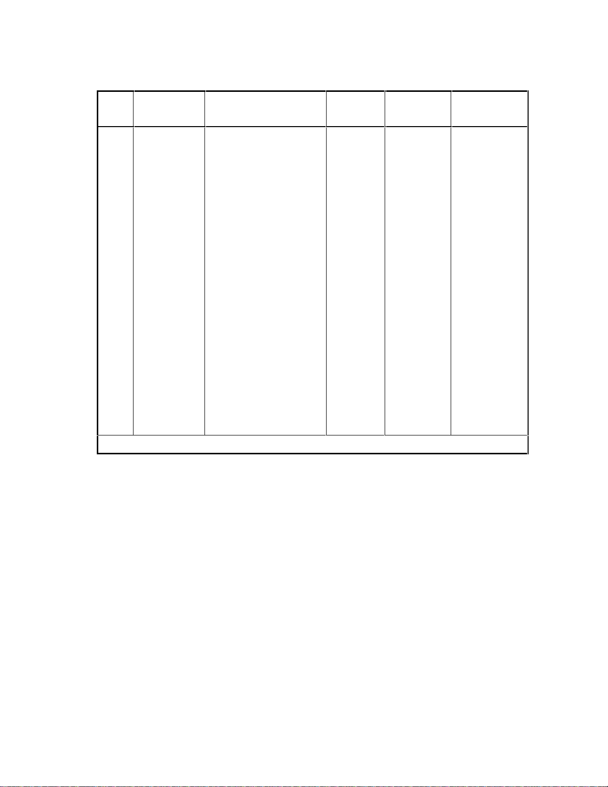
Configuration and Installation
Table 2–33. AT Expansion Bus Connector, C0-C19 (P2)
Pin
C0
C1
C2
C3
C4
C5
C6
C7
C8
C9
C10
C11
C12
C13
C14
C15
C16
C17
C18
C19
Signal
Name Function In/Out
GND
SBHE
LA23
LA22
LA21
LA20
LA19
LA18
LA17
MEMR*
MEMW*
SD8
SD9
SD10
SD11
SD12
SD13
SD14
SD15
Key
Ground
Bus High Enable
Address bit 23
Address bit 22
Address bit 21
Address bit 20
Address bit 19
Address bit 18
Address bit 17
Memory Read
Memory Wr ite
Data Bit 8
Data Bit 9
Data Bit 10
Data Bit 11
Data Bit 12
Data Bit 13
Data Bit 14
Data Bit 15
Key Pin
N/A
I/O
I/O
I/O
I/O
I/O
I/O
I/O
I/O
I/O
I/O
I/O
I/O
I/O
I/O
I/O
I/O
I/O
I/O
N/A
Drive
Level PU/PD/S *
N/A
12 mA
24 mA
24 mA
24 mA
24 mA
24 mA
24 mA
24 mA
12 mA
12 mA
12 mA
12 mA
12 mA
12 mA
12 mA
12 mA
12 mA
12 mA
N/A
33 S, 10K PU
33 S, 10K PU
4.7K PU
4.7K PU
4.7K PU
4.7K PU
4.7K PU
4.7K PU
4.7K PU
4.7K PU
* PU = pull up; PD = pull down; S = resistance in series. All values in ohm s .
2–35
Page 55

CoreModule/3SXi Technica l Manua l
Table 2–34. AT Expansion Bus Connector, D0-D19 (P2)
Signal
Pin
D0
D1
D2
D3
D4
D5
D6
D7
D8
D9
D10
D11
D12
D13
D14
D15
D16
D17
D18
D19
* PU = pull up; PD = pull down; SER = resistance in series. All values in ohm s .
Name Function In/Out
GND
MEMCS16*
IOCS16*
IRQ10
IRQ11
IRQ12
IRQ15
IRQ14
DACK0*
DRQ0
DACK5*
DRQ5
DACK6*
DRQ6
DACK7*
DRQ7
+5V
MASTER*
GND
GND
Interrupt Request 10
Interrupt Request 11
Interrupt Request 12
Interrupt Request 15
Interrupt Request 14
DMA Acknowledge 0
DMA Acknowledge 5
DMA Acknowledge 6
DMA Acknowledge 7
Ground
16-bit Mem Access
16-bit I/O Access
OUT
DMA Request 0
OUT
DMA Request 5
OUT
DMA Request 6
OUT
DMA Request 7
+5 Volt Power
Bus Master Assert
Ground
Ground
N/A
IN
IN
IN
IN
IN
IN
IN
IN
IN
IN
IN
N/A
IN
N/A
N/A
Drive
Level PU/PD/S *
N/A
N/A
N/A
N/A
N/A
N/A
N/A
N/A
6mA
N/A
6mA
N/A
6mA
N/A
6mA
N/A
N/A
N/A
N/A
N/A
330 PU
330 PU
27K PU
27K PU
27K PU
27K PU
27K PU
330 PU
2–36
Page 56

Configuration and Installation
2.13.5 Interrupt and DMA Channel Usage
The AT bus provides several interrupt and DMA control signals. W hen you expand the system with
MiniModule products or plug-in cards that require either interrupt or DMA support, you must select
which interrupt or DMA channel to use. Typically this involves switches or jumpers on the module. In
most cases, these are not shared resources. It is important that you configure the new module to use an
interrupt or DMA channel not already in use. For your convenience, Table 2–35 and Table 2–36 provide a
summary of the normal interrupt and DMA channel assignments on the CoreModule/3SXi CPU.
Table 2–35. Interrupt Channel Assignments
Interrupt Function
IRQ0
IRQ1
IRQ2
IRQ3
IRQ4
IRQ5
IRQ6
IRQ7
IRQ8
IRQ9
IRQ10
IRQ11
IRQ12
IRQ13
IRQ14
IRQ15
* Unavailable on the PC/104 bus.
ROM BIOS clock tick func tion, fr om Tim er 0 *
Cascade input for IRQ8-15 *
Reserved for battery-backed clock alarm *
IDE hard disk controller
Keyboard interrupt *
Serial 2
Serial 1
Available
Floppy controller
Parallel port
Available
Available
Available
Available
Available
Available
2–37
Page 57

CoreModule/3SXi Technica l Manua l
Table 2–36. DMA Channel Assignments
Channel Function
0
1
2
3
4
5
6
7
Available for 8-bit transfer s
Available for 8-bit transfer s
Floppy controller
Available for 8-bit transfer s
Cascade for channels 0-3
Available for 16-bit transfer s
Available for 16-bit transfer s
Available for 16-bit transfer s
2–38
Page 58

CHAPTER 3
OPERATION
3.1 INTRODUCTION
This chapter provides the information you need to software configure your CoreModule/3SXi CPU. The
first section describes the SETUP function. It describes each option that can be set using SETUP.
Additional sections describe important options you can set for each major functional block of the board.
Note
The SETUP descriptions in the following section also contain much
useful information about each SETUP topic. Review these sections
even if you already know how to set the SETUP parameters.
This chapter presumes you have some familiarity with DOS (PC-DOS, MS-DOS, or DR DOS). It does
not attempt to describe the standard DOS and ROM BIOS functions. Refer to the appropriate DOS and
PC reference manuals for information about DOS, its drivers and utilities, and about the software
interface of the onboard ROM-BIOS. Where Ampro has added to or modified standard functions, these
will be described.
The Ampro Common Utilities manual contains detailed descriptions of the Ampro utility programs
supplied on the Utility diskette that is included with the CoreModule/3SXi CPU Development Kit.
3.2 SETUP OVERVIEW
Many options provided on the CoreModule/3SXi CPU are controlled by the SETUP function. You have
access to these options when you activate the SETUP function. The parameters are displayed on four
screens. To configure the board, you modify the fields on these screens and save the results in the
onboard configuration memory. The configuration memory consists of portions of the CMOS RAM in
the battery-backed real-time clock chip and an Ampro-unique configuration EEPROM. To enhance
embedded-system reliability, the contents of the EEPROM mirror the contents of the CMOS memory.
The EEPROM retains your configuration information even if the clock’s backup battery should fail. If
you choose to use the CoreModule/3SXi CPU without a battery, the system takes its SETUP parameters
from the EEPROM, providing battery-free operation.
The SETUP information is retrieved from configuration memory when the board is powered up or when
it is rebooted with a CTL-ALT-DEL key pattern. Changes made to the SETUP parameters (with the
exception of the real-time clock time and date settings) do not take effect until the board is rebooted.
The SETUP function is located in the ROM BIOS. It can be accessed using CTRL-ALT-ESC while the
computer is in the Power On Self Test (POST), just prior to booting up. This is called hot key access.
The screen will display a message indicating when you can enter CTRL-ALT-ESC. You may also enter
the SETUP function from the DOS command line using the SETUP.COM program provided on the
Ampro Common Utilities diskette .
3–1
Page 59

CoreModule/3SXi Technical Manual
Table 3–1 summarizes the choices found on each SETUP page.
1. Functions on Each SETUP Page
Page Menu Name Functions
1 Standard (CMOS/EEPROM)
Configuration
2 Options/Peripheral
Configuration
3 Extended SCSI and Hard
Disk configuration
Set date and time
Define floppy drives
Define IDE hard disks
Select video type
Display DRAM quantity
Set error halt conditions
Enable/disable video shadow RAM
Set POST display option
Enable/disable extended BIOS functions
Enable/disable APM BIOS functions
Enable/disable serial ports
Enable/disable/configure parallel port
Enable/disable floppy interface
Enable/disable IDE interface
Configure Mono/Color
Enable/disable hot key access to SETUP
Set video display state
Select POST display option
Configure byte-wide and OEM Flash memories
Enable/disable serial boot loader
Enable/disable watchdog timer
Set SCSI controller parameters
Configure SCSI disk map
Select floppy or hard disk boot
Configure DOS disk map
4 Extended Serial Console
Configuration
* SETUP pages 3 and 4 are available when you enable Extended BIOS from SETUP
3–2
Configure serial port parameters for serial
console output
Configure serial port output handshake option
Configure serial port parameters for serial
console input
Delete/include console port from DOS COM
table
Page 60

Note
Some SETUP options can put your system into an unrecoverable
state. For instance, you might set a display option that prevents
you from seeing the SETUP screens. Installing a jumper between
J3-7 and J3-8 (Serial 1 DTR and RI) temporarily sets all SETUP
functions to their default state, bypassing the SETUP parameters
stored in the configuration memory so that you can reenter SETUP
and correct the problem.
Operation
3–3
Page 61

CoreModule/3SXi Technical Manual
3.3 SETUP PAGE 1—STANDARD (CMOS) SETUP
The first SETUP page contains the parameters normally saved in CMOS RAM plus some additional
parameters unique to the CoreModule/3SXi CPU. The only parameters not also saved in the EEPROM
memory are the real-time clock date and time. If no battery is used or if the battery fails, the date and
time will not be accurate. All other parameters are saved in the EEPROM.
Figure 3–1 shows what can be configured using SETUP page 1. Sections following the figure describe
each option.
Standard (CMOS/EEPROM) Setup
Date (mm/dd/yy) 9/20/96 Time (hh:mm:ss) 10:08:00
1st Floppy 1.4M
2nd Floppy 1/2M
Cyls Heads Sectors Precomp Landzone
ATA/IDE Disk 1 17 655 14 17 0 0
ATA/IDE Disk 2 None
Video EGA/VGA
Base Memory 640
Extended Memory 1024
Error Halt NO HALT ON ANY ERROR
Video Shadow RAM Enabled
System POST Normal
PgDn or (D)own for Extended Setup
áá ââ [Enter] Moves Between Items, ßßàà + - Selects Values
(E)xit to quit without change, or (S)ave to record changes
Figure 3–1. SETUP Page 1
3.3.1 Date and Time
The time shown on the first SETUP screen is continuously updated and reflects the current state of the
hardware real-time clock. The new time and date that you enter is immediately written to the device.
Enter the date in the form mm/dd/yy. Enter the time in 24-hour format, in the form hh:mm:ss.
The ROM BIOS maintains the system real-time clock. It is incremented approximately 18.2 times per
second by an interrupt from timer/counter 0. The ROM BIOS automatically initializes the system realtime clock from the hardware real-time clock upon system reset or power up. The accuracy of the
hardware real-time clock depends, of course, on your connecting a battery to the appropriate terminals
3–4
Page 62

Operation
on J5, the Utility connector. If no battery is attached, the system time information will not remain
accurate after a power cycle.
3.3.2 Floppy Drives
The ROM BIOS supports all of the popular DOS-compatible floppy disk formats. This includes all the
5-1/4 inch and 3-1/2 inch floppy formats—360K, 720K, 1.2M, and 1.44M. (Note: some formats are not
supported by early versions of DOS.) In addition, the ROM BIOS supports dual-capacity use of high
density floppy drives. That is, you can read and boot from 360K floppies in a 1.2M 5-1/4 inch drive, and
from 720K floppies in a 1.44M 3-1/2 inch drive.
Drive Parameter Setup
Enter the number and type of floppy drives in the system. If the drives connected to the system do not
match the parameters in the configuration memory, POST displays an error message. To eliminate the
error message, set the drive parameters to match your floppy drives.
3.3.3 IDE Hard Disk Drives
The ROM BIOS supports one or two hard disk drives connected to the IDE interface. The BIOS allows
you to mix IDE drives in combination with SCSI hard disk drives. (Use the IDE SETUP parameters for
IDE drives only. SCSI hard drives are configured on SETUP screen 3.)
The IDE SETUP parameters are used for setting the physical parameters of the drives you install in your
system. Physical drives can have one or more logical partitions. You can install up to eight logical
drives or drive partitions, but only two physical drives. (Older versions of DOS may limit the number of
logical drives you can install.)
To configure the system for one or two IDE drives, set the drive parameters with SETUP, as outlined
here:
n Drive Types—The configuration memory contains a default list of parameters that specify the
physical format of each drive. Each type specifies the total number of cylinders, the number of
sectors per cylinder, number of heads, cylinder to begin precompensation, and landing zone cylinder
number. The drive manufacturer supplies these parameters. The list contains “legacy values”,
standard for PCs—a number of older (smaller) drives are defined.
Two special drive types, 48 and 49, let you enter drive parameters manually. If no built-in drive type
matches your drive, select drive type 48 or 49 and enter the drive parameters in the fields provided.
Drive type AUTO selects Autoconfigure. Autoconfigure queries the drive for its parameters. Most
modern drives will respond to the query, allowing the BIOS to set the drive parameter values
automatically. This option also provides Logical Block Addressing (LBA) capability, which is used
to support drives larger than 512M bytes.
3–5
Page 63

CoreModule/3SXi Technical Manual
Note
LBA uses a translation scheme to convert physical heads, sectors
and cylinders to logical block numbers. Due to differences in the
translation schemes used by different system BIOSes, LBAcompatible drives that have been formatted on Ampro systems may
not function properly in other systems that support LBA mode.
However, due to the intelligent translation algorithm in the Ampro
BIOS, drives formatted in other systems are likely to be usable on
the CoreModule/3SXi CPU. Note that this only applies to IDE
drives that support LBA mode. Consult the technical literature for
your specific drive to find out if it supports LBA mode.
n Drive Selection—Besides specifying the physical characteristics of each IDE drive, you also must
specify how they are to be used by the ROM BIOS. Two factors control how they are used, drive
number jumper(s) and the DOS disk map.
1. An IDE drive can be jumpered as a master or slave. Each manufacturer’s drive is different, so
you must refer to the drive’s technical literature to find out how to jumper the drives you install.
Drives default to master from the factory, so if you only have one IDE drive in a system it is
generally already set up properly.
2. Use the SETUP Extended SCSI and Hard Disk Configuration menu (SETUP page 3) to enter
your IDE drive(s) in the DOS disk map. Disk 1 in the map will be logged by DOS as drive C,
Disk 2 as drive D, and so on. See the description of SETUP page 3 for details.
Once you have set the system’s configuration memory, the IDE drive(s) can be formatted and otherwise
prepared normally. Refer to your operating system and disk drive documentation for specific procedures
and requirements.
3.3.4 Video
Specify the initial video mode. Select Mono, Color40, Color80, or EGA/VGA. If your video display
card is VGA, super VGA, or any other high resolution standard, specify EGA/VGA no matter how it is
configured to come up.
3.3.5 DRAM Memory
The ROM BIOS automatically sets the amount of memory it discovers during Power-On Self-Test
(POST) and stores the result when you save the configuration values when exiting SETUP. If you change
the amount of memory installed on the board, however, you must run SETUP and do a save when you
exit. This updates the configuration memory to reflect the new memory size. Until you do this, an error
message will appear during POST.
Note that if an error message appears during POST when you have not changed the amount of memory
installed, it indicates that at least part of the memory is not functioning properly.
3.3.6 Error Halt
Select which kinds of errors will halt the POST. If you plan to use the module without a keyboard, be
sure to set this option to not halt on keyboard error.
3–6
Page 64

Operation
3.3.7 Video Shadow RAM
This option, when enabled, allows the ROM BIOS to copy the contents of a video BIOS into DRAM.
The actual video BIOS ROM on the video controller is disabled, and DRAM is mapped into the address
space it occupied. This speeds up video BIOS accesses. Ampro video controllers are designed to allow
video BIOS shadowing. If you are using a video controller from another manufacturer, it may not
support shadowing. In that case, set video BIOS shadowing to “Disabled.”
3.3.8 System POST
At boot time, the BIOS runs a series of tests called the “Power On Self Test”, or POST. There are
options in the Ampro BIOS to customize the POST to control how fast the computer powers up and to
control what the user sees at power up time. The choices are:
n Normal—Displays the results of all tests
n Fast—Faster than Normal POST because it uses a shorter memory test
n Express—Skips most tests and does not display POST test results on the screen
3–7
Page 65

CoreModule/3SXi Technical Manual
3.4 SETUP PAGE 2—OPTIONS/PERIPHERAL CONFIGURATION
Use SETUP page 2 to enable or disable many of the functions and peripherals provided on the
CoreModule/3SXiCPU. Figure 3–2 shows what can be configured on SETUP page 2, and the sections
that follow describe each parameter.
CM/3SXi Options/Peripheral Configuration
CoreModule Extended BIOS ............ Enabled
Advanced Power Mgmt BIOS ............ Enabled
Serial Port 1 ....................... Enabled
Serial Port 2 ....................... Enabled
Parallel Port ....................... Enabled Mode SPP
Floppy Interface .................... Enabled
IDE Interface ....................... Enabled
Mono/Color Jumper ................... Color
Socket S0 ........................... 64K @ D0000h
OEM Flash ........................... 64K @ E0000h
Default Socket ...................... S0
Video State ......................... Enabled
Blank POST Test ..................... Enabled
Serial Boot Loader .................. Disabled
Watchdog Timer ...................... Disabled
Hot Key Setup ....................... Enabled
(S)ave to Record Extended Setup
áá ââ [Enter] Moves Between Items, ßßàà + - Selects Values
(E)xit to quit without change, or (S)ave to record changes
Figure 3–2. SETUP Page 2
3.4.1 Extended BIOS
Normally, the Ampro Extended BIOS is enabled. This allows access to SETUP pages three and four and
the features they define. If you do not want to use the BIOS extensions, you can disable them using this
parameter. (Some UNIX implementations or other operating systems may require disabling the
extended portion of the BIOS.) Ampro Application Note AAN-9210 documents the features in the
extended BIOS, including the application program interface specifications.
3.4.2 Advanced Power Management BIOS
The CoreModule/3SXi CPU BIOS incorporates an Advanced Power Management BIOS (APM)
compliant with Advanced Power Management (APM) BIOS Interface Specification Revision 1.1, created
3–8
Page 66

Operation
by Intel and Microsoft. This SETUP option allows you to enable or disable access to the APM BIOS
functions. Note that this option does not enable or disable power management on the CoreModule, it
enables or disables access to the APM BIOS that drivers or applications use to control power
management features.
3.4.3 Serial Ports
Use SETUP to independently enable or disable either of the two onboard serial ports. (When you use
SETUP to enable or disable a port, the change does not take effect until you reboot the system.)
The I/O addresses and interrupt assignments (IRQs) for the serial ports cannot be changed. The
following table lists the I/O addresses and IRQs of each port. These resources are freed for use by other
peripherals installed on the PC/104 bus when their respective ports are disabled.
Table 3–2. Serial Port Resources
Port Address Interrupt
Serial 1 3F8h – 3FFh IRQ4
Serial 2 2F8h – 2FFh IRQ3
Normally, the BIOS logs Serial 1 and Serial 2 as COM1 and COM2. Note, however, that COM1 and
COM2 are logical designations, not physical values. When the system boots, the BIOS scans the
standard serial port addresses and installs the first port it finds as COM1. If it finds a second port, it
installs that one as COM2, and so on. If you disable a serial port, the designations of all highernumbered COM ports will change.
For more information about the serial ports, see Serial Ports, page 3—21.
3.4.4 Parallel Port
You enable or disable the CoreModule/3SXi parallel port using the Parallel Port option on this SETUP
page. You set the parallel port mode (SSP, EPP, or ECP) by setting the Mode option.
Table 3–3 summarizes the resources that are used when the parallel port is enabled.
3. Parallel Port Resources
Selection I/O Address Interrupt
Primary 0378h - 037Fh IRQ7
Disable None None
The I/O ports and interrupt request channel are freed for use by other peripherals installed on the
PC/104 bus when the parallel port is disabled.
Normally, the BIOS logs in the primary and secondary parallel ports as LPT1 and LPT2. Note, however,
that LPT1 and LPT2 are logical designations, not physical values. When the system boots, the BIOS
scans the standard parallel port addresses and installs the first port it finds as LPT1. If it finds a second
3–9
Page 67

CoreModule/3SXi Technical Manual
port, it installs that one as LPT2, and so on. If you disable a parallel port, the designations of all
higher-numbered LPT ports will change.
Setting the Parallel Port Mode
Set the parallel port mode to either SPP, EPP, or ECP.
Table 3–4 Parallel Port Modes
Mode Description
SPP Standard Parallel Port (default)—Bi-directional, compatible
with standard and PS/2 ports.
EPP Enhanced Parallel Port—Bi-directional, compatible with
standard and PS/2 ports, but adding automatic read- and
write- cycle modes.
ECP Extended Capabilities Port—IEEE-1284-compliant port.
Provides interlocking handshaking, 16-byte FIFO buffer,
optional DMA transfer capability, and optional RLE data
compression.
For more information about the parallel port, see Enhanced Parallel Port on page 3–25.
3.4.5 Floppy Interface Enable
Enable or disable the onboard floppy interface. When disabled, the I/O ports assigned to the floppy
controller become available, allowing them to be used by other devices installed on the expansion bus.
Table 3–5 lists the resources used by the floppy controller.
5. Floppy Controller Resources
Selection I/O Address IRQ DMA
Enabled 03F2h Digital Output Register
03F4h Main Status Register
03F5h Data Register
03F7h Control Register
Disable None None None
IRQ6 DMA 2
3.4.6 IDE Interface Enable
Enable or disable the onboard IDE hard disk interface. When disabled, the I/O ports and IRQ assigned
to the IDE controller become available, allowing them to be used by other devices installed on the
expansion bus. Table 3–6 lists the resources used by the IDE interface.
3–10
6. IDE Controller Resources
Selection I/O Address Interrupt
Enabled 01F0h - 01F7 Control and Data Registers IRQ14
Page 68

Operation
03F7h Shared with FDC
Disable None None
If you have an IDE drive attached to J6, just disabling the IDE interface will not free the interrupt,
IRQ14, since it is connected directly to the drive. You must disconnect the cable.
3.4.7 Mono/Color Selection
Set the Mono/Color selection to Mono only if you have a monochrome monitor connected to a
monochrome (MDA) video adapter. In all other cases, set this option to Color. Set it to Color even if you
have a VGA monochrome monitor attached to a VGA or SuperVGA adapter.
3.4.8 Hot Key Setup Enable
In some embedded systems, you do not want an end-user to use the hot-key sequence (CTRL-ALT-ESC)
to enter SETUP. You can enable or disable hot-key access to SETUP with this parameter. (This also
prevents “+++” from entering SETUP when using the serial console feature.)
3.4.9 Video State
You can set this option to Enabled or Inhibited. Inhibited blanks the display until your program makes
a call to the Video Restore State function in the video BIOS (via INT10h). This provides a means of
controlling what appears on the screen when the system starts up. This option can be used to inhibit the
POST test display and everything else that DOS or an application would display, until a call is made to
the video BIOS.
The following is an example of code that reenables the display inhibited by this option:
;=====================================================================
init: mov ah,1ch
mov al,-1
mov bx,414Dh
mov cx,5052h
int 10h
;=====================================================================
3.4.10 Blank Post Test
Enable or disable POST display. If set to Disabled, the messages from the POST will not be sent to the
console. To inhibit display of a broader range of system and application messages, see Video State,
above.
3–11
Page 69

CoreModule/3SXi Technical Manual
3.4.11 Byte-Wide Socket and OEM Flash Memory Configuration
The byte-wide socket, S0, and the user portion of the OEM Flash memory device can be independently
configured for its starting address and the size of the memory block in which it appears to the processor,
or it can be disabled. You can also specify which device is enabled at boot time. (This is the “Default
Socket” SETUP option.) Note that only one can be enabled at boot time.
Table 3–7 lists the socket address configuration options that are available.
7. Byte-Wide Memory and Onboard Flash Configuration
Size Address
Disabled None
64K bytes D0000h – DFFFFh
64K bytes E0000h – EFFFFh
128K bytes
(Available only for S0)
If you configure both devices to occupy the same address space (or overlap), only one device will be
visible to the CPU. This will be either the default socket (enabled during POST) or the socket that was
last enabled. The Ampro BIOS provides a call for enabling and disabling each device. A code example
is shown on page 3–30. Refer to Ampro Application Note AAN-9210 for a complete description of the
BIOS functions that control the byte-wide sockets.
Devices larger than 64K can be installed in the byte-wide socket, independent of the memory block size
setting. The memory block size setting specifies a “window” in which the memory device is visible.
You can use an extended BIOS call to select which 64K page of the byte-wide device is visible to the
processor. A code example is shown on page 3–31.
You must also set hardware jumpers to configure the byte-wide socket for the device you install in S0.
Refer to Chapter 2 for jumper positions. If you are using the byte-wide socket for Solid State Disk
(SSD), using Ampro’s Solid State Disk software, follow the directions for setting the byte-wide socket
that are in the SSD Technical Manual.
D0000h – EFFFFh
3.4.12 Serial Boot Loader Enable
This parameter enables or disables the Serial Boot Loader option in the Ampro ROM BIOS. The serial
boot loader allows you to boot from either of the onboard serial ports, much in the same way you would
boot from a local hard disk or from a LAN. A description of the Serial Boot Loader is provided in the
Ampro Common Utilities manual (see SERLOAD and SERPROG), and in Ampro Application Note
AAN-9403. If you are not using the Serial Boot Loader, set this parameter to “Disabled.”
3–12
Page 70

Operation
3.4.13 Watchdog Timer Configuration
This parameter allows you to set the time duration of the watchdog timer for monitoring the boot
process. You can set it to 30, 60, or 90 seconds, or you can disable it.
Further information about the watchdog timer can be found later in this chapter under “Watchdog
Timer.” A description of the WATCHDOG utility program can be found in the Ampro Common
Utilities manual.
3–13
Page 71

CoreModule/3SXi Technical Manual
3.5 SETUP PAGE 3—SCSI HARD DISK
A unique feature of the CoreModule/3SXi CPU is that its ROM BIOS contains hard disk support
functions that allow easy integration of SCSI and IDE drives. Use this SETUP screen to configure for
your hard disk drives and other SCSI peripherals. Figure 3–3 shows SETUP screen 3, and descriptions
of each field are provided in sections below.
Extended SCSI and Hard Disk Configuration
SCSI /BIOS Services............. Enabled
SCSI Initiator ID............... 7
SCSI Disk I/O Retries........... 10
SCSI Disk Map
SCSI 1.......................... Id 0, Lun 0
SCSI 2.......................... Not Active
SCSI 3.......................... Not Active
SCSI 4.......................... Not Active
SCSI 5.......................... Not Active
SCSI 6.......................... Not Active
SCSI 7.......................... Not Active
DOS Disk Map
Default Boot Device............. Floppy
1st Hard Disk................... SCSI Disk 1
2nd Hard Disk................... IDE Disk 1
3rd Hard Disk................... Not Active
4th Hard Disk................... Not Active
5th Hard Disk................... Not Active
6th Hard Disk................... Not Active
7th Hard Disk................... Not Active
8th Hard Disk................... Not Active
áá ââ [Enter] Moves Between Items, ßßàà + - Selects Values
(E)xit to quit without change, or (S)ave to record changes
Figure 3–3. SETUP Page 3
With the Ampro Extended BIOS, SCSI hard disks are available to DOS through standard ROM BIOS
functions (INT 13). (SCSI interface hardware is available on a variety of Ampro add-on products.) SCSI
functions are in the SCSI BIOS portion of the ROM BIOS. The ROM BIOS hard disk support allows
direct system booting from SCSI Common Command Set direct access devices. Other types of SCSI
direct access devices can be used to provide a compatible hard disk function. These include CD ROM
drives, tape drives, SCSI RAM disks, and other peripherals.
Most DOS or Windows applications run normally in this SCSI-based hard disk environment. Programs
nearly always use either DOS or ROM BIOS functions for disk drive access. It is rare for software to
attempt to access hard disk controller hardware directly.
Utilities for SCSI drive formatting, and other SCSI functions are included on the Ampro Common
Utilities diskette. These are described in the Ampro Common Utilities manual.
3–14
Page 72

Operation
3.5.1 SCSI Drive Parameter Setup
If you add a SCSI device to your CoreModule/3SXi-based embedded system, you must set several SCSI
drive parameters in the configuration memory using SETUP. This section describes the SETUP
parameters found on the SCSI Disk Configuration screen.
SCSI Controller Parameters
n SCSI/BIOS Services—To use the SCSI BIOS for hard disks, it must be enabled. When disabled, the
system will not boot from an attached SCSI drive, nor will standard disk-related BIOS calls (INT13)
be able to see a drive. SCSI services are still available from BIOS calls in your program, even when
SCSI/BIOS Services is disabled. Disabling the SCSI BIOS services will speed up system booting
when you don’t use the SCSI port.
n SCSI Initiator ID—The Ampro CoreModule/3SXi CPU is the SCSI Initiator in its transactions with
SCSI target devices such as hard disk drives. Every SCSI device (target or initiator) must have a
unique ID between 0 and 7. The default ID for the SCSI controller on the CoreModule/3SXi CPU is
7. It is the highest priority ID, and this ID tells the SCSI BIOS to reset the SCSI bus on system
power up or reset. In most cases you will not change the default SCSI initiator ID.
n SCSI Disk I/O Retries—You can specify the number of read/write retries when using SCSI drives
as DOS drives. The default is 10 retries.
SCSI Disk Map
n Target Device IDs and LUNs—The specification of SCSI target device IDs and Logical Unit
Numbers (LUNs) are stored in the configuration memory. Enter the IDs and LUNs of the SCSI
drives you have installed in your system. Assign each drive to a SCSI Disk position in the SCSI
Disk Map. Normally, all SCSI LUNs default to 0.
The SCSI ID for target devices can be 0 to 6 (since the CPU is set for ID 7). A device’s ID is usually set
by jumpers or switches on the device. If you have multiple SCSI drives, assign each one a unique
device ID.
DOS Disk Map
n BOOT Device Specification—You can choose to boot the system from a hard or floppy drive using
the Default Boot Device parameter. You can specify Floppy for floppy A: or Hard Disk for drive C:.
(When you select Hard Disk, the drive shown as 1st Hard Disk on the DOS Disk Map becomes the
boot drive.)
n DOS Disk Map—Assign your disk drives, both IDE drives and SCSI drives, to positions on the
DOS Disk Map. You can assign them in any order and in any mix. The 1st Hard Disk becomes
drive C:, 2nd Hard Disk becomes drive D:, and so on. Any non-SCSI devices that will appear to
the system as a drive should be configured in the DOS Disk Map as an AT Bus Drive. This includes
any device that is installed with its own driver.
3–15
Page 73

CoreModule/3SXi Technical Manual
SETUP screen 1, “Standard (CMOS) SETUP” is used for defining
hard drives connected to the IDE interface. Do not attempt to use
the IDE configuration menu to define disk drive parameters for
SCSI-connected drives.
Note
3–16
Page 74

Operation
3.6 SETUP PAGE 4—SERIAL CONSOLE
The ROM BIOS includes a unique set of features which allow full access to the system at any time over
standard RS232 serial ports. An embedded system may take advantage of these remote access
capabilities using the serial console functions in the following ways:
Serial console—Use Serial 1 or Serial 2 as a console. Use a serial terminal to replace the standard video
monitor and keyboard.
Serial boot loader—Boot from a serial port much like you would boot from a local hard disk or from a
network. (This feature is enabled or disabled with the Serial Boot Loader option on Page 2 of SETUP.)
Serial programming—Automatically update system software, such as an SSD, through a serial port.
This feature allows you to replace code in a Flash device installed in the byte-wide socket.
For more information about these serial console functions, see “Serial Console Features,” under “Serial
Ports”, later in this chapter. For a thorough explanation of the remote host features, refer to Ampro
Application Note AAN-9403.
Figure 3–4 shows the options you can set for the serial console. Since the DOS normally initializes the
serial ports during boot, you have the option to remove the serial console port from DOS’s COM port
table. By doing this, the values you set on SETUP screen 4 will remain after you boot DOS.
Extended Serial Console Configuration
Console Output Device......... Video
Console Input Device.......... Keyboard
Serial Console Output Setup
Data Length.................
Stop Bits...................
Parity......................
Baud........................
Delete from Com Port Table..
Console Output Handshake......
Serial Console Input Setup....
Data Length.................
Stop Bits...................
Parity......................
Baud........................
Delete from Com Port Table..
NOTE: When the Console Output Device is serial, the
MONO/COLOR jumper must be removed and the
Video in Standard Setup set to EGA/VGA.
áá ââ [Enter] Moves Between Items, ßßàà + - Selects Values
PgUp or (U)p for previous page
Figure 3–4. SETUP Page 4
3–17
Page 75

CoreModule/3SXi Technical Manual
Console Output Device—Select the console output device, either Video, Serial 1, Serial 2, or None.
Console Input Device—Select the console input device, either the PC Keyboard, Serial 1, Serial 2, or
None.
Serial Console Output Setup—Enter the communication parameters for your console output serial port.
Set the data length, stop bits, parity, and baud rate to match your serial output device.
Console Output Handshake—Enable or disable hardware handshaking. If enabled, the DSR and CTS
signals control the data flow. Be sure to connect the DSR and CTS signals on the serial port’s connector
to the appropriate handshake signals on the external serial device’s interface connector.
Serial Console Input Setup—Enter the communication parameters for your console input serial port.
Set the data length, stop bits, parity, and baud rate to match your serial input device.
Delete from COM Port Table—When DOS boots, it initializes the system serial ports. (Different
versions of DOS may set the ports to different default settings.) By enabling this option, the BIOS does
not include your console serial device(s) in the COM port table. This prevents DOS from changing the
values you assign to the port in this SETUP screen.
Caution
Be careful when changing the console configuration. If you specify
“None” for console input and output, there will be no console
access to the system. (You can recover from this state by removing
the serial console plug from the primary serial port connector and
shorting pins J3-7/8.)
3.7 THE SETUP.COM PROGRAM
You can use the SETUP.COM utility from the command line to access the same SETUP functions as the
“hot key” code, CTRL-ALT-ESC. SETUP.COM also adds additional functionality, such as the ability to
load and store configuration settings to a disk file. This same feature is used to store up to 512 bits of
OEM information in the configuration memory EEPROM. SETUP.COM is on the Ampro Common
Utilities diskette, included with the CoreModule/3SXi CPU Development Kit.
3.7.1 Creating Configuration Files with SETUP.COM
The Ampro SETUP utility, SETUP.COM, offers the following options for command line entry:
SETUP [-switches] [@file.ext | Wfile.ext]
3–18
Page 76

Operation
The supported switches and their meaning are as follows:
Table 3–8. SETUP.COM Command Switches
Switch Function
? Display a usage help screen
T Set the (hardware) real-time clock time and
date from the current DOS time and date.
@file.ext Writes the specified file to the board’s
CMOS RAM and configuration EEPROM.
Drive and path are optional in the file name.
Wfile.ext Write CMOS RAM and EEPROM contents to
the file specified. The file name may contain
an optional drive and path.
You can save a copy of the current contents of the board’s configuration memory to a disk file by using
the W switch. The data saved includes the entire contents of the nonvolatile configuration EEPROM.
The first 512 bits are the SETUP information (excluding time and date). The next 512 bits are available
for OEM storage. See Ampro Application Note AAN-8805 for a description of how to use the OEM
storage portion of the EEPROM.
Note
If the SETUP is changed, the system must be rebooted before
writing a configuration file using the SETUP W option. Otherwise,
the changes will not appear in the setup file.
The file you create with this menu option can be used as a source for programming the configuration
memory of a CoreModule/3SXi CPU at a later time.
For example, the following command initializes the EEPROM values with a previously saved
configuration:
C>SETUP @SYSTEM.A
Assuming you created the file SYSTEM.A with SETUP’s write option, SETUP will initialize the
EEPROM configuration memory and CMOS RAM using the contents of SYSTEM.A.
Note
The system must be rebooted before new configuration information
will take effect.
Using SETUP to save and load configuration memory parameters can be useful when many boards must
be initialized automatically, for instance, during production, or when you want to change between
several predefined system configurations.
3–19
Page 77

CoreModule/3SXi Technical Manual
3.8 OPERATION WITH DOS
The CoreModule/3SXi CPU supports IBM’s PC-DOS or Microsoft’s MS-DOS, Version 3.3 or later, or
any version of Digital Research’s DR DOS as the disk operating system. Any differences between these
similar operating systems are noted in the text where applicable.
Caution
Sometimes MS-DOS is customized by a manufacturer for a specific
system and may not work on the CoreModule/3SXi CPU. Use DR
DOS (supplied by Ampro), IBM PC-DOS (supplied by IBM), or the
generic version of MS-DOS (supplied by Microsoft on an OEM
basis).
EMS Option—The CoreModule/3SXi CPU can emulate the Lotus-Intel-Microsoft Expanded Memory
Specification Version 4.0 (LIM EMS 4.0), with the memory management capability of the 80386SX
CPU, under control of a device driver. Such drivers are available with the newer versions of DOS. With
Microsoft MS-DOS, the driver is called EMM386.EXE.
Serial Ports—DOS normally supports the board’s two serial ports as COM1 and COM2.
At boot time, DOS initializes the serial ports, assigning them their COM port designations and their
communication parameter settings. Although this might vary with different types and versions of DOS,
typical communication parameter settings are 9600 baud, even parity, 7 bits, and 1 stop bit.
Usually an application program that uses a serial port will access the port’s hardware and reinitialize the
communication parameters to other values, based on settings that the user has entered when configuring
the application program.
Parallel Port—The Parallel Printer port is normally the DOS LPT1 device. Most application software
uses LPT1 as the default printer port. If you enable the port, printing to it is automatic.
The following DOS commands can be used to test printing with a parallel printer:
A>COPY filename.ext LPT1 Prints contents of filename.ext
A>DIR >LPT1 Prints the directory
In addition, the <PrtSc> (Print Screen) key will print the contents of the video screen to the LPT1
device. Also, you can use the Printer Echo function to print all characters typed on the keyboard. The
command <Ctrl-P> enables the Printer Echo function. Entering <Ctrl-P> again disables Printer Echo.
Disk Drives—Older versions of DOS require you to divide disk drives larger than 32M bytes into more
than one partition. More recent versions permit drives to be up to 2G bytes, though IDE drives are BIOS
limited to 512M bytes. Drives larger than 512M bytes must use the Auto configuration type in SETUP
or use a vendor supplied driver to access the entire drive.
3–20
Page 78
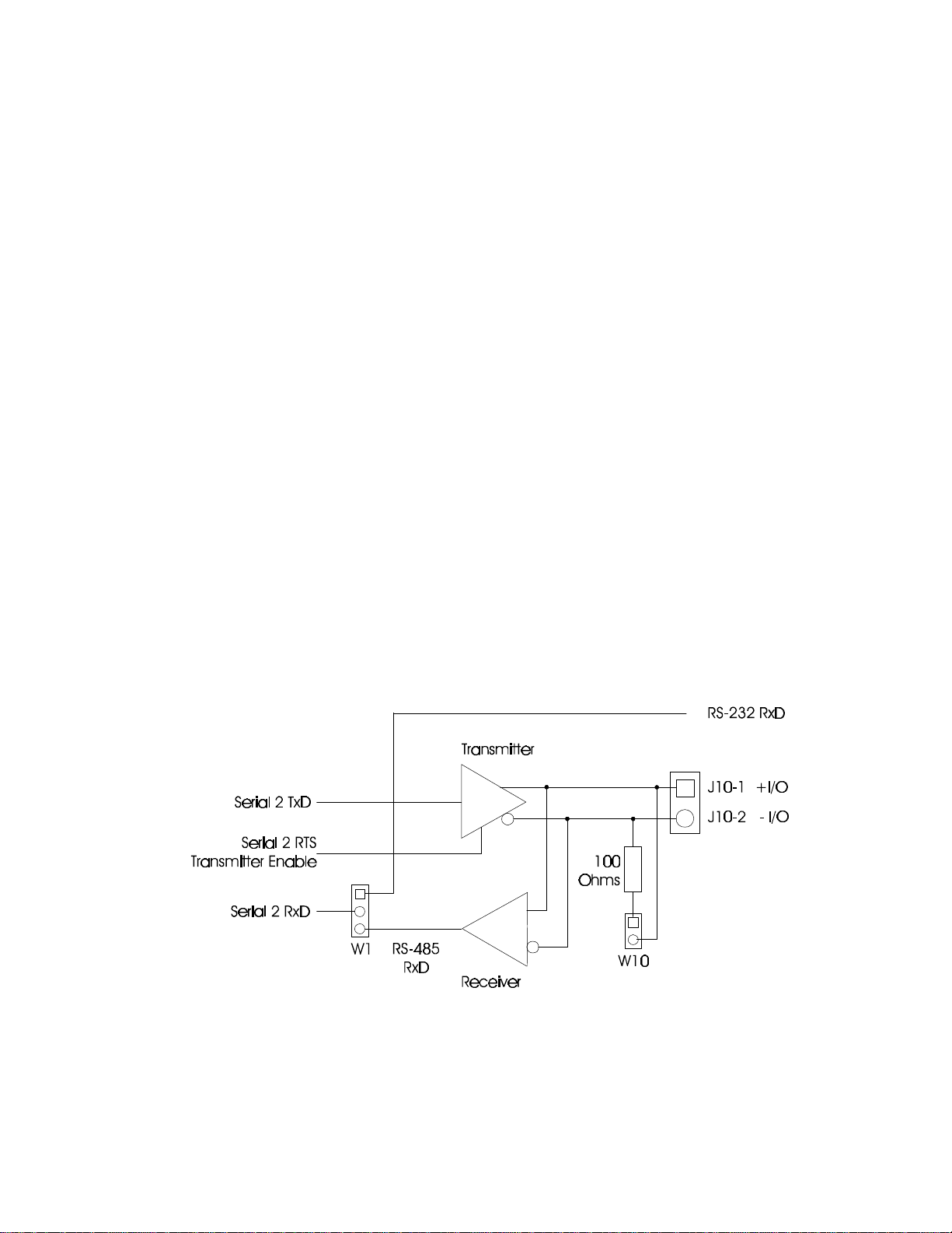
Operation
3.9 SERIAL PORTS
This section describes uses for the serial ports on the CoreModule/3SXi CPU, including:
• Using the RS-485 interface
• The serial console feature
• Serial booting
• Serial downloading and programming
• Using a serial modem
3.9.1 Using the RS-485 Interface
This section describes the RS-485 interface circuit and discusses some RS-485 concepts to aid in using
the interface in an embedded system.
RS-485 provides for half-duplex operation. It is a 5 volt differential interface, which has greater
immunity against noise and interference than single-wire interfaces. This interface will drive cable
lengths up to 4000 feet reliably at 57.6K bps. All communication, both transmission and reception,
occurs via a single pair of wires. There are no handshaking lines.
RS-485 supports multidrop operation. That is, more than two devices can be connected to the same
RS-485 balanced line. To prevent signal contention, only one transmitter is enabled at a time. The
CoreModule/3SXi RS-485 transmitter is controlled by Serial 2’s RTS signal. At power up, RTS is in its
inactive state, ready to receive. When it is time to transmit, the RTS signal is made active, enabling the
transmitter. It is the responsibility of the user’s software to prevent two transmitters from being enabled
at the same time.
Figure 3–5 illustrates the CoreModule/3SXi RS-485 interface wiring.
5. RS-485 Interface Wiring
The following are some examples of interconnection schemes that can be used to take advantage of the
RS-485 serial connection:
3–21
Page 79

CoreModule/3SXi Technical Manual
n One-way Broadcast—A single device uses an RS-485 signal pair to transmit data to many
receiving devices. To enable the broadcaster’s transmitter, the RTS signal is turned on (True, High,
Active) and left on. If the device is to be a receiver, RTS must be turned off and left off.
n Simple Bi-Directional Communication—Two devices use a single RS-485 bi-directional pair for
half-duplex, two-way transmission of data. The Adapter’s transceiver is placed in the send or
receive mode under control of the network software. This can be done using a simple alternation
scheme or by messages contained within data packets.
n Multidrop Network—More than two devices share an RS-485 signal pair, for both transmission
and reception of data. Only one device is permitted to talk at any one time. As with simple bidirectional communication, the board’s RS-485 transceiver is placed in receive mode unless it is the
one permitted to transmit. One popular way of managing who is the transmitter is by a “token
passing scheme. Each node is assigned an ID number. Whoever transmits also sends the ID of the
next node allowed to transmit. If a node does not need to transmit, it just immediately sends the
“token” to its next node. This simple scheme is easy to implement and trouble free. Time-outs can
be implemented in software to prevent a lockup should a node fail to pass the token properly.
3.9.2 Serial Console Features
To use the serial console features, connect the serial console device(s) to Serial 1 or Serial 2. Use
SETUP to configure the CoreModule/3SXi CPU to use its serial console support feature. The
configuration memory stores serial console configuration parameters.
Caution
Be careful when changing the console configuration using SETUP.
If you specify “None” for console input and output, there will be no
console access to the system. (You can recover from this state by
removing the serial console plug from the primary serial port
connector and shorting pins J3-7/8.)
SETUP provides separate configurations for serial console input and output. Thus, you can use a serial
port (and attached serial device) for either or both input and output. For instance, you can use a modem
or other serial device for input, and a standard video display for output. Or you can use a standard
keyboard for input and an ASCII terminal for serial display, or use an ASCII terminal for both input and
output.
To use an ASCII terminal as the console device for your system, set both the input and output
parameters to Serial Port 1 (or 2), and set the serial baud rate, data length, and stop bits to match the
setting of your terminal. For proper display of SETUP and POST messages from the BIOS, you must use
an IEEE-compatible terminal that implements the standard ASCII cursor commands. The required
commands and their hexadecimal codes are listed in Table 3–9.
3–22
Page 80

Table 3–9. Required Serial Console Commands
Hex Command
08 Backspace
0A Line Feed
0B Vertical Tab
0C Non-destructive Space
0D Carriage Return
Note
Some programs that emulate an ASCII terminal do not properly
support the basic ASCII command functions shown in Table 3–9.
Ampro provides a suitable PC terminal emulator program,
TVTERM, on the Common Utilities diskette.
Operation
After booting this system, the keyboard and screen of the terminal become the system console. The
programs you use this way must use ROM BIOS video functions (rather than direct screen addressing)
for their display I/O. You can enter keyboard data from both the external serial device and the standard
AT keyboard.
Note
DOS programs that write directly to video RAM will not display
properly on a serial console device.
COM Port Table
When the system boots, DOS initializes the serial ports to 9600 baud (typical). To preserve the selected
console port parameters stored in SETUP, the ROM BIOS can be instructed to delete the selected
console port from the internal COM port table, normally used by DOS to locate the serial ports. With the
port deleted from the COM port table, DOS cannot change its parameters. If you use a serial console, be
sure to select the option that deletes the console port from the COM port table.
Serial Handshake
The serial console device data format and the CoreModule/3SXi CPU serial port data format must match
for the devices to properly communicate. In addition, the hardware handshake behavior must be
compatible. Normally, a serial port’s Data Set Ready (DSR) and Clear To Send (CTS) input handshake
signals must be true (active) for the ROM BIOS to send data out. On the CoreModule/3SXi CPU, the
hardware handshake can be enabled or disabled with SETUP. When hardware handshaking is enabled,
be sure to connect the DSR and CTS signals to appropriate handshake signals on the external serial
device’s interface connector. As an alternative, loop the CoreModule/3SXi’s serial output handshake
signals to its input signals as follows:
3–23
Page 81

CoreModule/3SXi Technical Manual
n DTR (out) to DSR (in)
n RTS (out) to CTS (in)
3.9.3 Serial Booting and Serial Programming
Serial console functionality has been expanded to incorporate two additional features useful in embedded
applications.
n The serial boot facility enables the CoreModule/3SXi CPU to boot from code downloaded through a
serial port in a manner similar to booting from a local hard disk or from a network.
n The serial programming facility permits updating Flash memory devices installed in the byte-wide
socket over the serial port. It can also be used to program the OEM Flash device.
Refer to Ampro Application Note AAN-9403 for a complete description of these features. Refer to the
Ampro Common Utilities manual for descriptions of SERLOAD and SERPROG, utility programs used
to support serial booting and serial programming.
3.9.4 Using a Serial Modem
You can use any of the RS232C ports as a modem interface. You will not need to concern yourself with
serial port initialization since most PC communications programs control the serial port hardware
directly. If your program does not do this, use the DOS MODE command to initialize the port.
When installing a modem, be sure to connect appropriate input and output handshake signals,
depending on what your communications software requires. Standard PC-compatible serial modem
cables that connect all of the proper signals correctly are commonly available. The signal arrangement
on the serial port connectors is described in Chapter 2.
Many powerful communications programs are available to control modem communications. Some of
these programs offer powerful “script” languages that allow you to generate complex automatically
functioning applications with little effort.
3–24
Page 82

Operation
3.10 ENHANCED PARALLEL PORT
The enhanced parallel printer port is a superset of the standard PC-compatible printer port. It supports
three modes of operation:
n Standard PC/AT printer port (SPP)—Centronics-type output only printer port, compatible with
the original IBM PC printer port. Sometimes it is called a PS/2-compatible parallel port. It behaves
the same as the standard PC/AT port on outputs, and provides an input mode as well.
n Enhanced Parallel Port (EPP)—Bi-directional parallel port, compatible with the Standard and
PS/2 ports, and adding automatic read- and write-cycle modes. Automatically generates input and
output handshaking signals for increased throughput. Data flow is monitored by a watchdog timer
(separate from the board’s watchdog timer) to ensure reliable transfers.
n Extended Capabilities Parallel Port (ECP)—Compliant with the IEEE-1284 Extended
Capabilities Port Protocol and ISA Standard (Rev 1.09, January 7, 1993), developed by Microsoft.
The ECP mode provides the highest level throughput for the parallel port. It provides interlocking
handshaking, a 16-byte FIFO buffer, DMA transfers (optional), hardware RLE data compression
(optional), and well-defined software protocols.
The low-level software interface to the parallel port consists of eight addressable registers. The address
map of these registers is shown in Table 3–10.
10. Parallel Port Register Map
Register Name Address
Data Port Base address
Status Port Base address + 1
Control Port Base address + 2
EPP Address Port Base address + 3
EPP Data Port 0 Base address + 4
EPP Data Port 1 Base address + 5
EPP Data Port 2 Base address + 6
EPP Data Port 3 Base address + 7
Note: EPP registers are only accessible when in
EPP mode
3.10.1 Standard and Bi-Directional Operation (SPP)
You can use the parallel port as a standard output-only printer port or as a bi-directional data port with
up to 12 output lines and 17 input lines. The bi-directional mode can be very valuable in custom
applications. For example, you might use it to control parallel-connected external peripherals, an LCD
display, scan keyboards, sense switches, or interface with optically isolated I/O modules. All data and
interface control signals are TTL-compatible.
To use the parallel port in standard or bi-directional modes, set the parallel port Mode option on page 2
of SETUP to SPP.
3–25
Page 83

CoreModule/3SXi Technical Manual
Note
Note that the term “mode” in this section is used for both the
SPP/EPP/ECP Mode as set with SETUP, and for input and output
modes that port can be in when in the SPP Mode. For clarity, the
port’s SETUP Mode setting will be in bold type and capitalized to
distinguish it from the various modes that the port can be in when in
the SPP Mode.
The default mode of the port in SPP Mode is output only, to make the port compatible with the original
IBM PC parallel port. To use the port as a bi-directional data port, put it in bi-directional mode with a
Ampro extended BIOS call, as shown in the following code example.
;---------------------------------------------------------; Code to set the parallel port mode to “bi-directional”
;----------------------------------------------------------
MOV AH,0CDh ; AMPRO command
MOV AL,0Ch ; AMPRO function
MOV BX,01h ; Bi-directional mode (00 for output-only)
INT 13h
Once the port is in bi-directional mode, you can dynamically change the port between input and output
states by directly accessing the control register at I/O address 37Ah.. The initial state of the port after
the BIOS call is input. A “1” written to 37Ah-bit 5 sets the port to input; a “0” sets it to output.
The following example is code for dynamically changing the primary parallel port’s direction (the code
assumes that the port is in SPP Mode).
;---------------------------------------------------------; Code to change the parallel port direction to input
;----------------------------------------------------------
MOV DX,37Ah
IN AL,DX
OR AL,20h ;set bit 5
OUT DX,AL
;
;---------------------------------------------------------; Code to change the parallel port direction to output
;----------------------------------------------------------
MOV DX,37Ah
IN AL,DX
AND AL,0DFh ;clear bit 5
OUT DX,AL
3–26
Page 84

Operation
Using control lines for Input/Output
Besides the eight data lines, you can use the four control lines (-STROBE, -AUTOFD, -INIT, and -SEL
IN) as general purpose output lines when the port is set to SPP Mode. Similarly, you can use the five
status lines (-ERROR, SEL OUT, PAPER EMPTY, -ACK, and BUSY) as general purpose input lines.
You can also read the four control lines and use them as input lines. These lines have open collector
drivers with 4.7K ohm pull-ups. To use a control line as an input line, you must first write to its
corresponding bit in the control register. Refer to Table 3-12 for the parallel port control register bit
definitions. If the line is inverting, write a “0”, otherwise write a “1”. This will cause the line to float
(pulled up by the 4.7K ohm resistors). When they float, you can use them as inputs. Table 3–11 is a
summary of the uses of the parallel port lines.
Table 3–11. Parallel Port Use
Signal
Type
Data
Control
Status
* Open collector control lines convert to TTL outputs in EPP and
ECP modes. Output under those conditions is 4 mA @ 2.4V
Parallel Port Interrupt Enable
Bit 4 in the control register, IRQEN, (see Table 3–12) enables the parallel port interrupt. If this bit is
high, then a rising edge on the -ACK (IRQ) line will produce an interrupt on IRQ7.
Number
of Lines Function Output Drive
8 lines
4 lines
5 lines
Read/Write
Read/Write*
Read Only
24 mA @ .5V
12 mA @ 2.4V
12 mA @.5V
4.7K PU
--
3–27
Page 85

CoreModule/3SXi Technical Manual
Table 3–12. Parallel Port Register Bits
Signal Name
Register Bit
DATA
(378h)
STATUS
(379h)
CONTROL
(37Ah)
0
1
2
3
4
5
6
7
0
1
2
3
4
5
6
7
0
1
2
3
4
5
6
7
or Function In/Out
Data 0
Data 1
Data 2
Data 3
Data 4
Data 5
Data 6
Data 7
0
0
0
ERROR*
SLCT
PE
ACK* (IRQ)
BUSY
STROBE*
AUTOFD*
INIT*
SLC
IRQEN
PCD
1
1
* Can also be used as input (see text).
I/O
I/O
I/O
I/O
I/O
I/O
I/O
I/O
In
---
--In
In
In
In
In
Out*
Out*
Out*
Out*
---
---
---
---
Active
High/Low
High
High
High
High
High
High
High
High
---
---
---
Low
High
High
Low
High
Low
Low
High
High
High
High
---
---
J15
Pin
3
5
7
9
11
13
15
17
---
---
---
4
25
23
19
21
1
2
6
8
---
---
---
---
DB25F
Pin
2
3
4
5
6
7
8
9
---
---
--15
13
12
10
11
1
14
16
17
---
---
---
---
3–28
Page 86

Operation
Register Bit Definitions
Table 3–13 defines the register bits shown in the “Signal Name or Function” column in Table 3–12.
13. Standard and PS/2 Mode Register Bit Definitions
Signal
Name Full Name Description
ERR* Error Reflects the status of the ERROR* input. 0
means an error has occurred.
SLCT Printer selected
status
PE Paper end Reflects the status of the PE input. 1
ACK* Acknowledge Reflects the status of the ACK* input. 0
BUSY* Busy Reflects the complement of the BUSY input. 0
STROBE Strobe This bit is inverted and output to the
AUTOFD Auto feed This bit is inverted and output to the
INIT* Initiate output This bit is output to the INIT* pin.
SLC Printer select
input
IRQEN Interrupt request
enable
Reflects the status of the SLCT input. 1
means a printer is on-line.
indicates paper end.
indicates a printer received a character..
indicates a printer is busy.
STROBE* pin.
AUTOFD* pin.
This bit is inverted and output to the pin. It
selects a printer.
When set to 1, interrupts are enabled. An
interrupt is generated by the positive-going
ACK* input.
PCD Parallel control
direction
PD0-PD7 Parallel Data Bits
When set to 1, port is in input mode. In
printer mode, the printer is always in output
mode regardless of the state of this bit.
3.10.2 EPP and ECP Operation
When set to either EPP or ECP Mode, the board’s parallel port is compliant with the IEEE-1284
Extended Capabilities Port Protocol and ISA Standard (Rev 1.09, January 7, 1993), developed by
Microsoft. The IEEE-1284 specification is complex and is beyond the scope of this manual. Contact
IEEE Customer Service and request IEEE Std 1284 for information about EPP and ECP operation.
3–29
Page 87

CoreModule/3SXi Technical Manual
IEEE Customer Service
445 Hoes Lane
PO Box 1331
Piscataway, NJ 08855-1331 USA
Phone: (800) 678-IEEE (in the US and Canada)
(908) 981-0060 (outside the US and Canada)
FAX: (908) 981-9667
Telex: 833233
3.11 BYTE-WIDE SOCKET
The 32-pin byte-wide memory socket S0 supports a variety of 28- and 32-pin JEDEC pinout memory
devices, including EPROM, Flash EPROM, NOVRAM, and SRAM. If you have a backup battery
attached to the Utility connector, you can configure the socket to supply backup battery power to convert
an SRAM into a Non-Volatile RAM (NOVRAM). Chapter 2 gives examples of the memory devices the
socket will support.
Ampro’s solid state disk (SSD) drive support in the ROM BIOS and optional SSD Support Software
treat the byte-wide socket as one or more DOS disk devices, containing up to 1M byte of storage. The
socket is highly configurable with jumpers to accept nearly any common JEDEC byte-wide device.
Instructions on how to configure the byte-wide socket for common devices are in Chapter 2.
Access Time
A device used in the byte-wide socket must have access times of 250 nS or less.
Content Mirroring
If you install a device smaller than the memory window specified in SETUP, (for example, a 32K byte
component in a 64K window) the contents will appear as multiple copies in the socket’s address
window.
OEM Flash Memory Device
The CoreModule/3SXi CPU has an onboard Flash memory, 64K of which is used to store the ROM
BIOS. The remainder is available for semi-permanent storage of programs or data. The amount of
available OEM Flash memory on the CoreModule varies between 64K and 960K, depending on the
model. Contact your Ampro sales representative for details about CoreModule/3SXi models.)
The onboard Flash memory is architecturally equivalent to a second byte-wide socket. It uses the same
software mechanisms in the BIOS to control access. It is also configured with SETUP in the same way
as the byte-wide socket. It is designated OEM Flash in SETUP.
The BIOS accesses the byte-wide S0 and the OEM Flash memory, S1, as 8-bit devices on the PC
expansion bus. If you are using both devices, your application program must manually enable and
disable them, as only one can be enabled at a time.
3.11.1 Accessing the Byte-Wide Socket and OEM Flash Device
To access the byte-wide socket or the OEM Flash device, it must be enabled. Using SETUP, you can
cause either device to be enabled at boot time. This places the contents of the enabled device at the
address you specified in SETUP and the processor can access this memory in a normal fashion. If you
want to use both the byte-wide socket and the OEM Flash device, you will need to enable each device as
it is needed, as only one can be enabled at a time.
3–30
Page 88

Operation
Here is a simple assembly language routine showing how to use an Ampro extended-BIOS call to enable
or disable the byte-wide memory socket, S0, or the OEM Flash memory. (This code selects the first 64K
page on large devices.) Note that when you enable a device, the BIOS call automatically disables the
opposite device.
;---------------------------------------------------------; Access control code for a byte-wide socket (S0 or the
; OEM Flash memory)
;----------------------------------------------------------
MOV AH,0CDH ; AMPRO function call
MOV AL,nn ; Use 03 for S0; 04 for the OEM Flash memory
MOV BL,nn ; Use 01 to turn ON or 00 to turn OFF
MOV BH,00 ; Selects page 0 of the device
MOV CX,414DH ; Ampro identifier(‘AM’)
INT 13H
3.11.2 Accessing Large Devices
For byte-wide devices over 64K bytes, select the 64K byte window size in SETUP. You then use software
to select which segment of the device you want to appear in that window, using code equivalent to that
illustrated below and using the values shown in Table 3–14. Table 3–14 gives the byte (in hex) to write
to the BH register to select each 64K segment of a large device.
This assembly language routine can be used to select pages when accessing large memory devices:
;---------------------------------------------------------; Page select code for a byte-wide socket (S0 or the
; OEM Flash memory)
;----------------------------------------------------------
MOV AH,0CDH ; AMPRO function call
MOV AL,nn ; Use 03 for S0; 04 for the OEM Flash memory
MOV BL,nn ; Use 01 to turn ON or 00 to turn OFF
MOV BH,x0h ; The upper nibble of BH contains the page
; number for devices larger than 64 K.
MOV CX,414Dh ; Ampro identifier (‘AM’)
INT 13H
3–31
Page 89

CoreModule/3SXi Technical Manual
Table 3–14. Segment Addressing in Large Memory Devices
Device
Size
128K 2 First BH=00h
256K 4 First BH=00h
512K 8 First BH=00h
1M 16 First BH=00h
64KB
Segments
Segment Address
(BH Value)
Second BH=10h
Second BH=10h
Third BH=20h
Fourth BH=30h
Second BH=10h
Third BH=20h
Fourth BH=30h
Fifth BH=40h
Sixth BH=50h
Seventh BH=60h
Eighth BH=70h
Second BH=10h
Third BH=20h
Fourth BH=30h
Fifth BH=40h
Sixth BH=50h
Seventh BH=60h
Eighth BH=70h
Ninth BH=80h
Tenth BH=90h
Eleventh BH=A0h
Twelfth BH=B0h
Thirteenth BH=C0h
Fourteenth BH=D0h
Fifteenth BH=E0h
Sixteenth BH=F0h
128K Special Case
If you install a 128K byte device in the byte-wide socket, you can set the starting address to D0000h and
the window size to 128K. It will occupy the entire D0000h - EFFFFh address region. This allows you to
access the entire device without switching between windows. (The 128K byte window size is not
available for the OEM Flash device, nor can it be used with Ampro’s SSD/DOS Support Software.)
3.11.3 Flash EPROM Programming
To program a Flash device in byte-wide socket S0 or the OEM Flash memory, use the FLASHWRI.EXE
utility supplied on the Common Utilities diskette. The Common Utilities manual describes its operation.
Programming power is handled automatically for both 5V and 12V Flash devices. The board provides
12V power for programming 12V Flash EPROMs. There are no jumpers to set (other than the Vpp
jumper, W2-6), as the onboard 12V Flash programming supply is controlled by software.
3–32
Page 90

Operation
You can also develop your own Flash programming routines using extended BIOS calls in the ROM
BIOS. Refer to Ampro Application Note AAN-9210 for information about the extended BIOS call
provided for Flash programming power. (Note that there is a 5 mS delay for the 12V Flash programming
supply to come up to its full voltage after being switched on by software.)
3.12 SCSI CONTROLLER
A SCSI controller can serve many purposes, including controlling hard disk drives, tape drives, text
scanners, and printer and communications servers. The ROM BIOS supports booting DOS from a SCSI
device such as a hard disk. With Ampro’s ROM BIOS support, you can use any device compatible with
the SCSI Common Command Set (CCS) for “direct access devices.” Ampro has several MiniModule
products that can be used to provide a SCSI interface for a CoreModule/3SXi CPU system.
The CoreModule/3SXi Development Kit comes with a diskette containing an assortment of SCSI
utilities for use with DOS. It includes a SCSI hard disk formatting utility that allows low-level
formatting and changing the disk interleaving. Refer to the Ampro Utilities manual for details about
using the SCSI utilities.
Besides direct access, SCSI devices include sequential access devices (tape), printer devices, read-only
devices (CD-ROM), and processor devices (CPUs). These device types require special application
programs, utilities, or driver software not included on the Ampro Utility diskette. Contact Ampro
Technical Support for information about connecting these devices to an Ampro SCSI interface.
Hard disk support for operating systems other than DOS may or may not be available through the ROM
BIOS hard disk driver. This depends on two things: whether the operating system in question uses
ROM-BIOS calls exclusively for the hard disk function; and whether the operating system has any
special ROM BIOS constraints, such as reentrancy. Some operating systems—multitasking ones in
particular such as UNIX—bypass the BIOS and attempt to program the hard disk controller directly.
With such systems, you must modify the operating system to add an appropriate SCSI hard disk driver
that can take advantage of the SCSI interface. An alternative is to use the IDE interface instead of
SCSI, as the IDE drive standard is more widely supported on PC platforms.
3.12.1 The Ampro SCSI BIOS
You can use a variety of mass storage devices with the SCSI universal bus interface and command
protocols. Ampro has added a further layer of universality, the SCSI BIOS.
The SCSI BIOS, a set of low level functions in the ROM BIOS, is a hardware-independent interface
between system software and SCSI peripherals. Using SCSI BIOS calls, programmers can write software
for SCSI devices without concern for the operational details of the SCSI interface. Also, the SCSI BIOS
enables you to import software from other environments more safely, quickly, and easily.
Application Note AAN-8804, available from Ampro, provides details of the SCSI BIOS functions.
3.13 PC SPEAKER
The CoreModule’s motherboard logic includes a standard AT-compatible speaker port. The speaker
logic signal is buffered by a transistor amplifier, and provides about 100 mW to an external 8 ohm
speaker.
The audio output is based on two signals: the output of Timer 2; and the programming of two bits, 0 and
1, at I/O port 61h. Bit 1 of I/O port 61h is one term of a 2-input AND gate. The other term is the output
3–33
Page 91

CoreModule/3SXi Technical Manual
from Timer 2. Thus, setting bit 1 to a logic 1 enables the output of Timer 2 to the speaker, and a logic 0
disables it. Disabling Timer 2 by setting bit 0 of port 61h to a 0 causes its output to go high. Then you
can use bit 1 of port 61h to control the speaker directly.
3.14 WATCHDOG TIMER
The purpose of a watchdog timer function is to restart the system should some mishap occur. Possible
problems include: a failure to boot properly; the application software losing control; temporary power
supply problems including spikes, surges, or interference; the failure of an interface device; unexpected
conditions on the bus; or other hardware or software malfunctions. The watchdog timer helps assure
proper start-up after an interruption.
The CoreModule/3SXi CPU ROM BIOS supports the board’s watchdog timer function in two ways:
n There is an initial watchdog timer setting, specified using SETUP, which determines whether the
watchdog timer will be used to monitor the system boot, and if so, how long the time-out is (30, 60,
or 90 seconds).
n There is a special ROM-BIOS function which may be used by application software to start, stop, and
retrigger the watchdog timer function.
The initial time-out should be set (using SETUP) to be long enough to guarantee that the system can
boot and pass control to the application. Once the system is booted and the application is running, the
application must periodically retrigger the timer so that a watchdog timer time-out does not occur. If
the time-out does occur, the system will respond in a manner determined by how the watchdog timer
jumper, W3, is set (see Chapter 2).
The following assembly language routine illustrates how to reset the watchdog timer using an Ampro
extended BIOS function call:
;---------------------------------------------------------; Watchdog timer control program
;---------------------------------------------------------MOV AH,0C3h ; Watchdog Timer BIOS function
MOV AL,nn ; Use “00” to disable; “01” to enable
; timer.
MOV BX,mm ; Selects time, in seconds
;(00-FFh; 1-255 seconds)
INT 15h
Ampro provides a simple DOS program that can be used from the command line or in a batch program
to manage the watchdog timer. It is called WATCHDOG, and is described in the Ampro Common
Utilities manual.
3–34
Page 92

Operation
Note
Some operating systems, including some versions of DOS, turn off
the real-time clock alarm at boot time. If your OS does this, make
sure that your application program enables the alarm function
using this BIOS call.
If you jumper the output of the Watchdog Timer to trigger a non-maskable interrupt (NMI), an NMI IO
Channel Check will be asserted by the real-time clock alarm circuit when it times out. For the system to
respond to the NMI, the NMI circuit must be enabled. (In the PC architecture, the non-maskable
interrupt can be masked.) To enable (unmask) the NMI, execute the following code.
;------------------------------------------------; To enable NMI (IO channel check)
;-------------------------------------------------
IN AL,61H
AND AL,NOT 08H
OUT 61H,AL
;-------------------------------------------------
To use the NMI I/O Channel Check in a custom Watchdog Timer handler routine, the standard NMI
handler would have to be replaced with your custom code. If you install your own NMI interrupt service
routine, it can test to see if the I/O Channel Check NMI occurred by reading I/O port 61h, bit 6. Bit 6 is
true (1) if the NMI occurred.
Note
Following the occurrence of an I/O Channel Check NMI, the
function must be disabled and then re-enabled before the next one
can occur.
3.15 POWERFAIL MONITOR
In embedded systems, it is important for the computer to execute a clean reset if its power supply
fluctuates. In general, you would want to avoid erratic behavior that could result if the system voltage
were to dip to marginal levels.
The CoreModule/386SXi has a built-in powerfail circuit that will generate a clean reset signal if power
falls below 4.65V. It guarantees a minimum 140 mS reset signal, independent of how long the power
falls below the 4.65V threshold.
3.16 SYSTEM MEMORY MAP
The CoreModule/3SXi CPU architecture allows it to address up to 64M bytes of memory. Table 3–15
shows how this memory is used.
The DRAM, the byte-wide socket, ROM BIOS, and OEM Flash memory occupy the first megabyte
(starting at 00000h). You can install up to 8 megabytes of DRAM onboard with 4M bytes of base DRAM
and a 4M byte custom add on memory module.
3–35
Page 93

CoreModule/3SXi Technical Manual
Table 3–15. CoreModule/3SXi Memory Map
Memory Address Function
FF0000h - FFFFFFh Duplicates BIOS at 0F0000-0FFFFFh.
100000h - FDFFFFh Extended memory
0F0000h - 0FFFFFh 64K ROM BIOS.
0D0000h - 0EFFFFh Byte-wide socket S0 or OEM Flash, if enabled.
0C0000h - 0CBFFFh VGA Video BIOS.
0A0000h - 0BFFFFh Normally contains video RAM, as follows:
000000h - 09FFFFh Onboard DRAM
Otherwise, free.
CGA Video: B8000-BFFFFh
Monochrome: B0000-B7FFFh
EGA and VGA video: A0000-AFFFFh
3.17 SYSTEM I/O MAP
Table 3-15 is a list of the I/O port assignments used on the CoreModule/3SXi CPU. The I/O port
functions and addresses (except for a few “Ampro reserved” addresses) shown in Table 3-15 are all
standard for PC compatibles from both a hardware and software perspective.
Typically, the ROM BIOS provides all the services needed to use the onboard devices and devices
connected to I/O ports. If you need to directly program the standard functions, refer to a programming
reference for the PC/AT.
3–36
Page 94

Table 3–16. CoreModule/3SXi I/O Map
I/O Address Function
03F8h - 03FFh Primary serial port
03F2h - 03F7h Floppy disk controller ports
3F2: FDC Digital output register
3F4: FDC Main status register
3F5: FDC Data register
3F7: FDC Control register
3F0, 3F1 Ampro reserved
0378h - 037Fh Parallel port (configured as Primary)
02F8h - 02FFh Secondary serial port
0278h - 027Fh Parallel port (configured as Secondary)
0202h Ampro reserved
01F0h - 01F7h IDE hard disk interface
00F0h - 00FFh Reserved
00C0h - 00DFh DMA controller 2 (8237 equivalent)
Operation
00A0h - 00A1h Interrupt controller 2 (8359 equivalent)
0092h Fast A20 gate and CPU reset
0080h - 009Fh DMA page registers (74LS61 equivalent)
0070h - 0071h Real-time clock and NMI mask
0060h, 0064h
0061h
0040h - 0043h Programmable timer (8254 equivalent)
0022h, 0023h Ampro reserved
0020h - 0021h Interrupt controller 1 (8359 equivalent)
0000h - 000Fh DMA controller 1 (8237 equivalent)
All I/O ports below 100h are reserved for internal system functions
and should not be accessed.
Keyboard controller (8042 equivalent)
Port B
Note
3–37
Page 95

CoreModule/3SXi Technical Manual
3–38
Page 96

INDEX
28-pin devices, in 32-pin sockets, 2–20
AAN-8702, 2–21
AAN-8804, SCSI BIOS, 3–33
AAN-8805, EEPROM access, 3–19
AAN-9003, 2–21
AAN-9210, Extended BIOS, 3–8, 3–33
AAN-9403, Serial boot, 3–12, 3–17, 3–24
AC termination, 2–31
AT bus, 2–29
Backplane, quality, 2–31
Balanced line, 3–21
Battery, 2–5
Calculating life, 2–5
Battery, external, 2–29
Battery-backed clock, 2–26
Bi-directional communication, 3–22
BIOS, SCSI, 3–33
Broadcast, 3–22
Bus termination, 2–31
Byte-wide, 1–3
Accessing large devices, 3–31
Addressing, 2–20
BIOS calls, 2–21
Configuration, 2–22, 3–12
Flash programming, 3–32
In memory map, 3–36
Serial programming, 3–17
Socket, 3–30
Socket signals, 2–25
Sockets, 2–19
COM port table, 3–24
Configuration
Summar y, 2 –3
Configuration, Byte-wide, 2–22
Connector
Parallel port (J15), 2–13
Coprocessor, math, 2–7
CPU, 1–1
CTRL-ALT-ESC, 3– 1
Cursor commands, 3–23
DC Power, 2–4
DIN plug, keyboard, 2–29
Direction, parallel port, 3–25
Disk, floppy, 2–14, 3–5
Disk, IDE, 2–16, 3–5
Disk, SCSI, 3–33
DMA, 2–37
DOS, 3–20
and SCSI, 3–33
MODE command, 3–24
DRAM, 2–6, 3–6
Embedded-PC System Enhancements, 1–7
EMS, 3–20
Environmental specifications, 1–8
Expanded memory, 2–6
Expansion bus, 1–2, 2–29
Expansion bus, ribbon cables, 2–31
Exte nd e d me mo ry , 2 – 6
External battery, 2–29
Cables, 2–2
Expansion bus, 2–31
Floppy, 2–15
IDE, 2–17
Keyboard, 2–28
Modem, 3–24
Parallel port, 2–12
Utility, 2–28
Clock, 2–26, 3–4
Filtering, PC bus, 2–31
Flash EPROMs, 2–24
Floppy drives, 2–14, 3–5
Floppy interface, 1–2, 2–14, 3–10
Half-duplex, 3–21
Hard disk drives, SCSI, 3–14
Hard drives, partitioning, 3–21
Hot key setup, 3–11
Index–1
Page 97

CoreModule/3SXi Technica l Manua l
I/O map, 3–36
IDE hard drives, 3–5
IDE interface, 1–2, 2–16, 3–10
IEEE 1284, 3–25, 3–29
Installation, custom, 2–2
Installation, MiniModules, 2–2, 2–30
Interface, floppy disk, 2–14
Interface, IDE, 2–16
Interrupts, 2–37
Jumpering, byte-wide, 2–22
Jumpering, general infor mation, 2– 3
LIM 4.0, 2–6, 3–20
Lithium battery, external, 2–29
Math coprocessor, 2–7
Mating connector (J15), 2–13
Mechanical specifications, 1–8
Memory map, 3–35
Memory, expanded, 2–6
Memory, extended, 2–6
MiniModule installation, 2–30
Modem, 3–23, 3–24
Motherboard, 1–1
Multidrop, 3–21, 3–22
Multimode Parallel Port, 3–25
Onboard Flash memory, 3–12
Parallel port, 1–2, 2–11, 3–21, 3–25
Parallel port configuration, 2–11
Parallel port connector (J15), 2–13
Parallel port, extended mode, 3–25
Partioning hard drives, 3–21
PC/104 bus, 1–2
Performance, system, 2–21
Port, Serial, 2–7
Ports, 3–20
POST, SETUP, 3 –7
Power requirements, 2–5
Power supplies, switching, 2–5
Power, DC, 2–4
POWERGOOD signal, 2–27
Printer port, 2–11
Pushbutton reset, 2–28
Real-time clock, 2–5, 2–26, 3–4
Reset, pushbutton, 2–28
RJ11 modular connector, 2–10
ROM BIOS, 3–20
ROM BIOS, video functions, 3–23
ROM-BIOS, extension, 2–21
RS-485, 2–9
RS-485 twisted-pair, 2–10
SCSI
BIOS, 3–33
Controller, 3–33
Utilities, 3–33
SCSI BIOS, 3–14
SCSI drive setup, 3–15
SCSI hard disk drives, 3–14
SCSI utilities, 3–14
Serial boot, 3–24
Serial boot loader, 3–12
Serial console, 3–22
Serial console option, 3–17, 3–24
Serial port, 1–1, 2–7, 3–9, 3–20
Serial programming, 3–24
SETUP, 2–6, 2–18, 2–20, 3–1
Setup, SCSI drives, 3–15
Shadowing, 2–6, 2–21, 3–7
Snubbers, 2–31
Solid state disk (SSD), 1–3, 3–30
Speaker, 2–28
Speaker, 3–33
SRAMs, 2–25
SSD, 1–3, 2–22
Switching power supplies, 2–5
System Expansion, 2–2
System, performance, 2–6
Termination, 2–10
Termination, AT bus, 2–29
Termination, floppy drives, 2–15
Termination, PC bus, 2–31
Timer, watchdog, 2–27
Token passing, 3–22
Index–2
Page 98

UNIX, 3–33
Utilities, SCSI, 3–33
Video, 3–23
Index
WATCHDOG, 3–34
Watchdog timer, 2–27, 3–12, 3–34
Index–3
 Loading...