

Page 1

ART6212 Datasheet
Amp’ed RF Technology, Inc.
www.ampedrftech.com
1
Page 2
ART6212 Product Specification
PRELIMINARY
Description
Amp’ed RF Tech presents the ART621 Wi-Fi &
BLE combo module: 802.11abgn/BLEv4.1. The
ART6212 is a small footprint low cost RF module
intended to help customers shorten product
development cycles and reduce cost.
Fully compatible with our AmpedUP embedded
protocol stack, the ART6212 may be matched
with many Host MCU chipsets. Additionally,
Linux and Android OS drivers are available.
The ART6212 is offered in WiFi/BLE combo,
WiFi only, and BLE only configurations.
12 mm x 12 mm x 2.4 mm
Features
WLAN
802.11a/b/g/n, 802.11d, 802.11r
Dual Band: 2.4GHz and 5GHz
Output Power, +21.5dBm
Interface, SDIO 2.0, SPI
Wi-Fi Direct (concurrent)
Wi-Fi Protected Setup
Soft Access Point
Hotspot 2.0
Security: WPA1/WPA2, AES, WEP
Blu et ooth
Bluetooth BLE 4.1
Hardw are
Serial interfaces: UART, SDIO
RoHS conformance
www.ampedrftech.com
2
Page 3

Contents
1. Hardware Specifications ....................................................................................... 4
1.1. Recommended Operating Conditions ............................................................................................ 4
1.2. Absolute Maximum Ratings ........................................................................................................... 4
1.3. Current Consumption .................................................................................................................... 4
1.4. Selected RF Characteristics .......................................................................................................... 6
1.5. Pin Assignment ART6212 ............................................................................................................. 8
1.6. Layout Drawing ART6212 ........................................................................................................... 10
2. Hardware Design ................................................................................................. 11
2.1. Module Reflow Installation ........................................................................................................... 11
3. Reference Design Example ART6212 ................................................................ 12
4. Startup behavior .................................................................................................. 15
4.1. WL_REG_ON & BT_RST_N ....................................................................................................... 15
4.2. UART and SPI interface .............................................................................................................. 15
5. RF Path Control ................................................................................................... 15
5.1. ART6212 Control ........................................................................................................................ 15
6. Ordering Information .......................................................................................... 16
7. Warning ................................................................................................................ 17
8. Revision History .................................................................................................. 17
www.ampedrftech.com
3
Page 4
1. Hardware Specifications
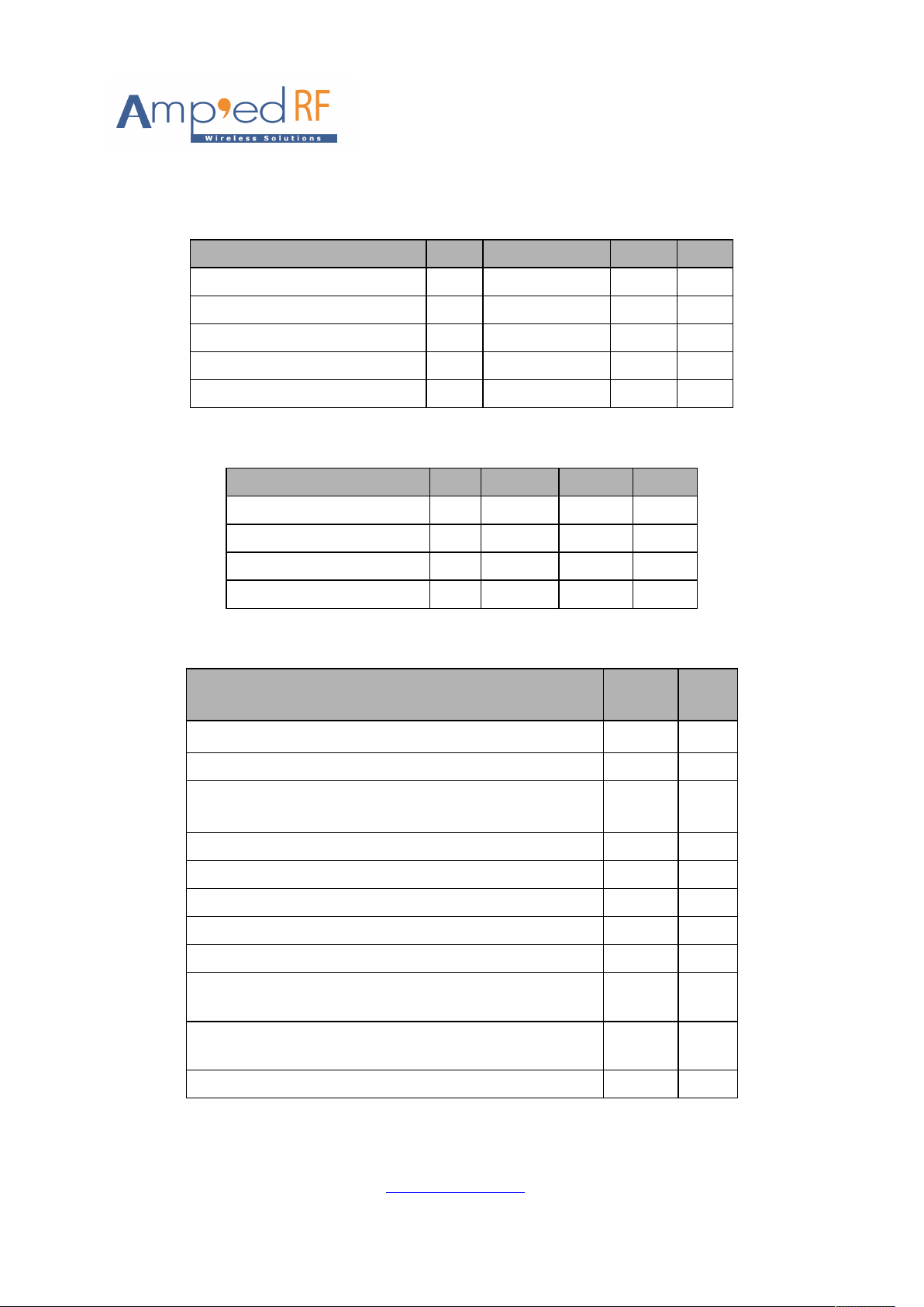
General Conditions (VIN= 3.6V and 25°C)
1.1. Recommended Operating Conditions
Rating Min Typical Max Unit
Operating Temperature Range -40 - 85 °C
Supply Voltage VIN 2.3 3.6 4.8 Volts
Supply Voltage V
Signal Pin Voltage - 0.7 V
RF Frequency 2400 - 2483.5 MHz
1.7 3.3 3.6 Volts
VDDIO
1.2. Absolute Maximum Ratings
Rating Min Typical Max Unit
Storage temperature range -55 - +150 °C
Supply voltage VIN -0.3 - +5.0 Volts
I/O pin voltage VIO -0.3 - +3.6 Volts
RF input power - - -5 dBm
1.3. Current Consumption
Modes (WLAN Max Power Consumption)
V
=3.6v
BAT
Complete Power Down (
Sleep 101 μA
WL_REG_ON
low)
VDDIO
~ V
- Volts
VDDIO
Avg Unit
17 μA
Power save (beacon period including DTIM 100ms, beacon length 1ms)
-proprietary power saving features enabled
RX (idle, 2.4GHz) 64.07 mA
RX (active, 2.4GHz, OFDM) 67.87 mA
TX (active, 2.4GHz, OFDM), 15.5dBm @RF port 242.67 mA
TX (active, 2.4GHz, OFDM), 20.5dBm @RF port 338.67 mA
TX (active, 2.4GHz, OFDM), 19.0dBm @RF port 285.67 mA
A VoIP call using a standard codec G.711 (64Kb/s, 320 byte packets) and
U-APSD (WMM power save) power-saving mode.
Video streaming; the device is receiving 2.0 Mbps of data using legacy
PSM mode (for example, MPEG-4@2Mbps)
Ipeak: system maximum peak current draw 378 mA
0.77 mA
4.65 mA
13.31 mA
www.ampedrftech.com
4
Page 5

Modes (Bluetooth Typical Power Consumption) Avg Unit
System reset mode 0.1 μA
System deep sleep mode TBD μA
Advertising (nonconnectable) (Interval: 1.28s;Data:15; bytes 3 channels) TBD μA
Advertising (discoverable) (Interval: 1.28 s;Data: 15 bytes;3 channels) TBD μA
Scanning (Interval: 1.28 s;Window: 11.25 ms;Single frequency per window) TBD μA
www.ampedrftech.com
5
Page 6
1.4. Selected RF Characteristics
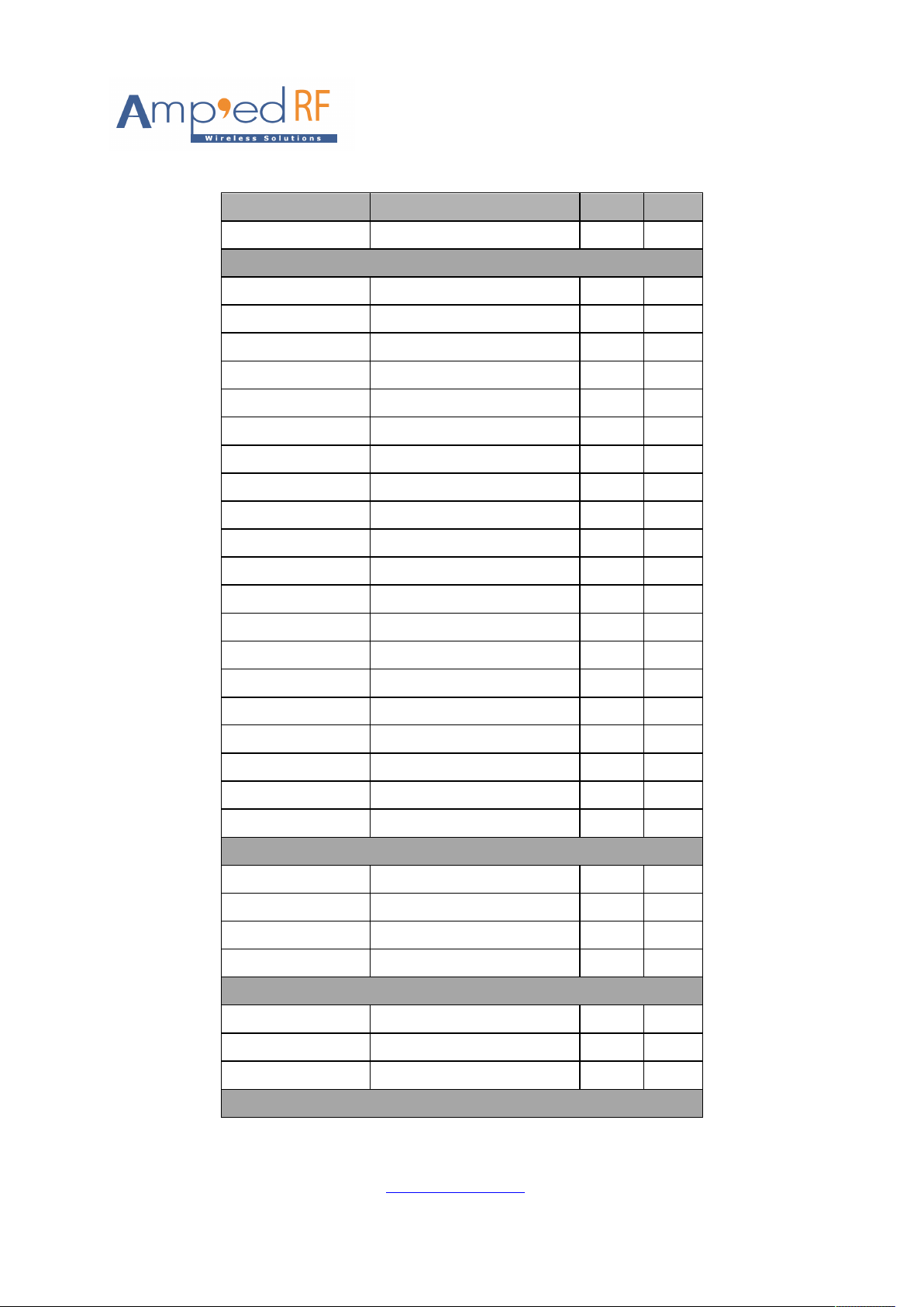
Parameters Conditions Typical Unit
Antenna load 50 ohm
Wi-Fi Receiver
Sensitivity DSSS 1Mbps@FER<8% -98 dBm
Sensitivity DSSS 2Mbps@FER<8% -95 dBm
Sensitivity CCK 5.5Mbps@FER<8% -93 dBm
Sensitivity CCK 11Mbps@FER<8% -91 dBm
Sensitivity BPSK 6Mbps@PER<10% -93.5 dBm
Sensitivity BPSK 9Mbps@PER<10% -91.5 dBm
Sensitivity QPSK 12Mbps@PER<10% -90.5 dBm
Sensitivity QPSK 18Mbps@PER<10% -88 dBm
Sensitivity 16QAM 24Mbps@PER<10% -85 dBm
Sensitivity 16QAM 36Mbps@PER<10% -82 dBm
Sensitivity 64QAM 48Mbps@PER<10% -78 dBm
Sensitivity 64QAM 54Mbps@PER<10% -76.5 dBm
Sensitivity BPSK 6.5Mbps@PER<10% -92 dBm
Sensitivity QPSK 13Mbps@PER<10% -89 dBm
Sensitivity QPSK 19.5Mbps@PER<10% -86.5 dBm
Sensitivity 16QAM 26Mbps@PER<10% -84 dBm
Sensitivity 16 QAM 39Mbps@PER<10% -80.5 dBm
Sensitivity 64QAM 52Mbps@PER<10% -76.5 dBm
Sensitivity 64QAM 58.5Mbps@PER<10% -74.5 dBm
Sensitivity 64QAM 65Mbps@PER<10% -73 dBm
Wi-Fi Receiver 5GHz 11n
Sensitivity BPSK 6.5Mbps@PER<10%,Nss=1 -91 dBm
Sensitivity QPSK 13Mbps@PER<10%, Nss=1 -88 dBm
Sensitivity 16QAM 26MbpsPER<10%,Nss=1 -83 dBm
Sensitivity 64QAM 65MbpsPER<10%,Nss=1 -72.5 dBm
Wi-Fi Transmitter
Output Power 802.11b@ch1 8 dBm
Output Power 802.11g @ch1 17.5 dBm
Output Power 802.11n @ch1 17 dBm
Wi-Fi Transmitter 5GHz, 11n
www.ampedrftech.com
6
Page 7
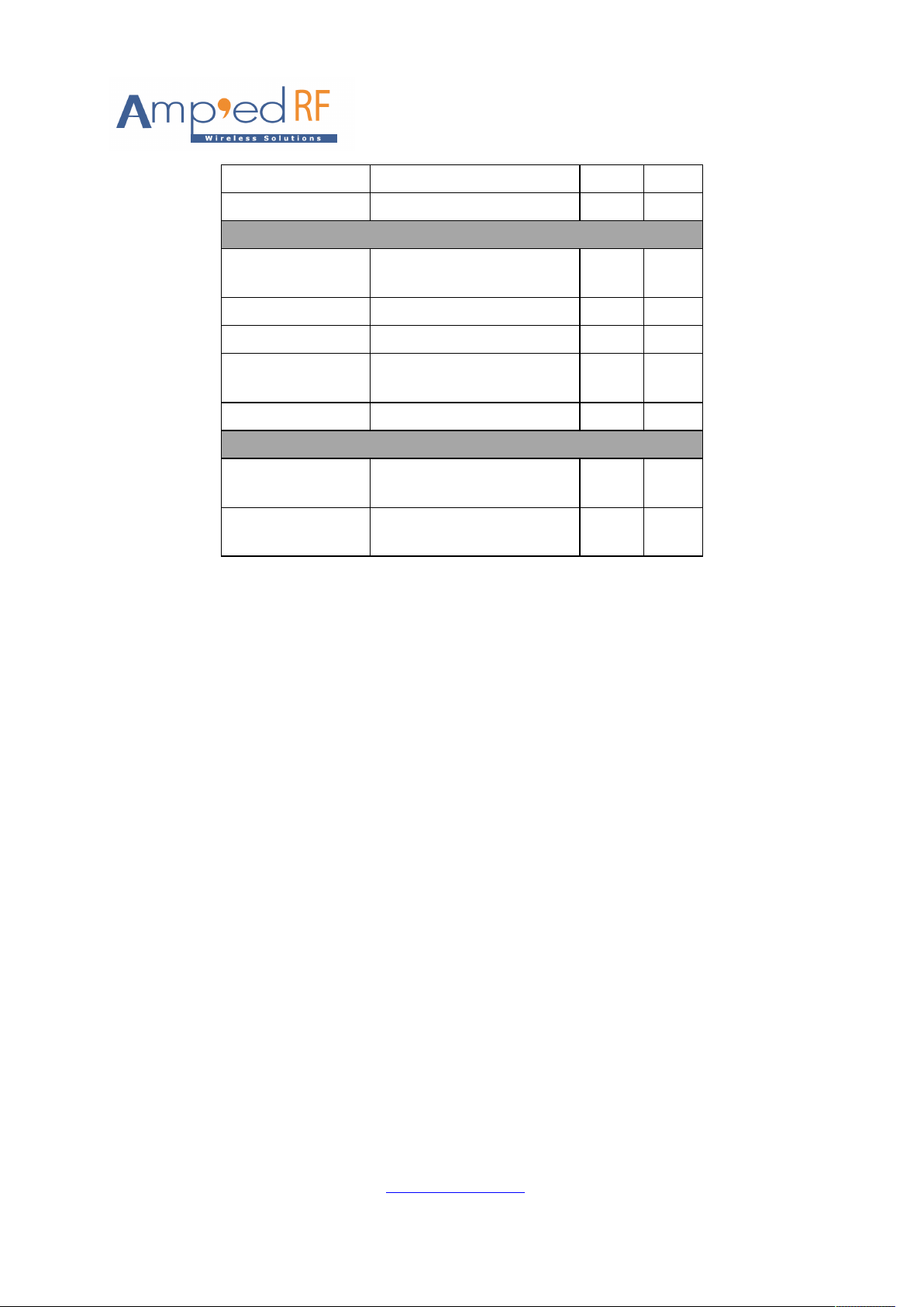
Output Power 802.11a @ch36 19 dBm
Output Power 802.11n @ch36 16 dBm
Bluetooth Transmitter
Frequency range
Maximum output power 2 dBm
Minimum output power -21 dBm
Minimum output power
in advertising mode
Output power accuracy TBD dB
Bluetooth Receiver
Receiver sensitivity
(clean transmitter)
Receiver sensitivity
(dirty transmitter)
TBD dBm
BER < .001 -93 dBm
BER < .001 TBD dBm
2400~24
83.5
MHz
www.ampedrftech.com
7
Page 8
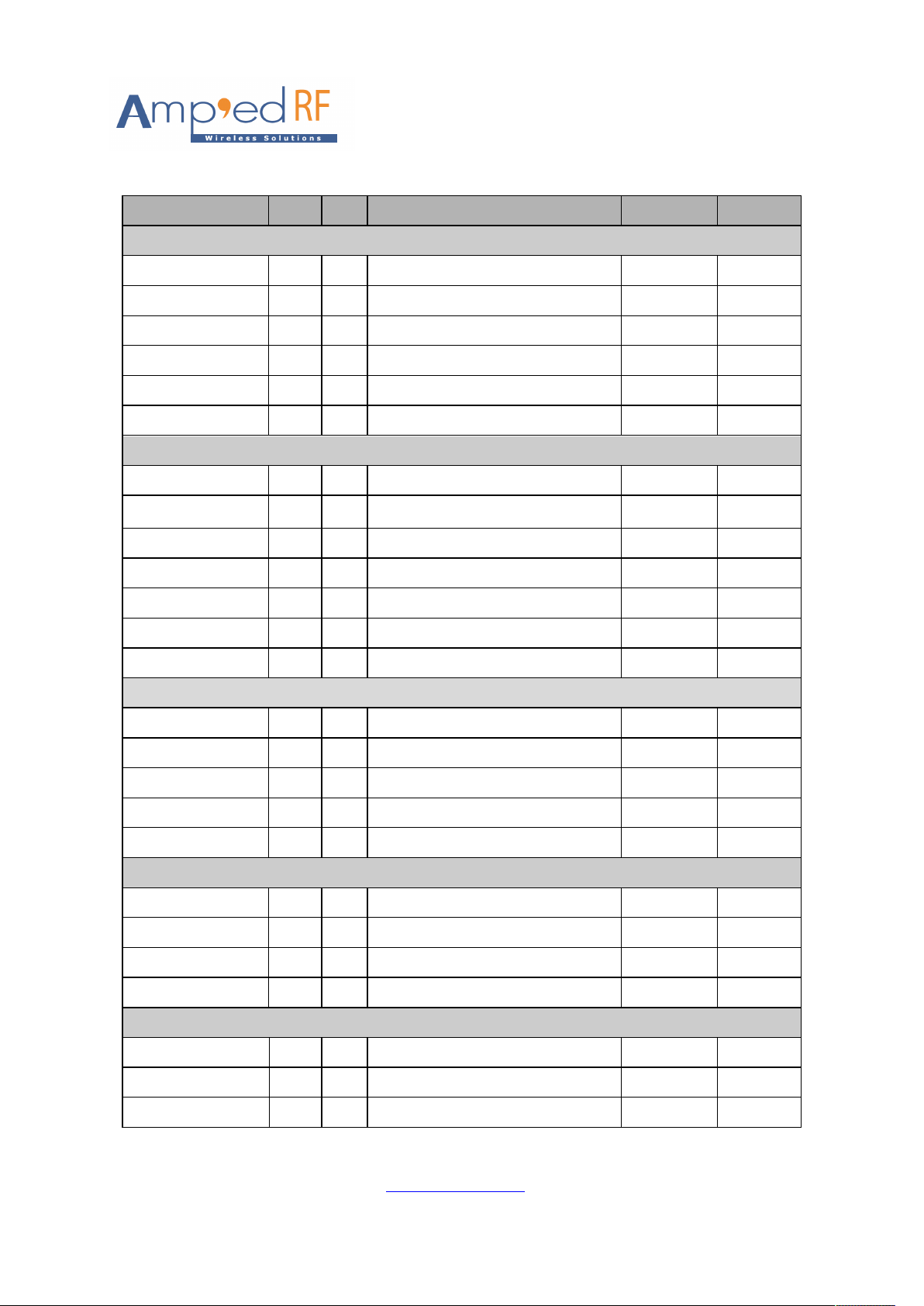
1.5. Pin Assignment ART6212
Name Type Pin # Description ALT Function Typ Voltage
Power and Ground
VIN
GND
9 VIN
20 GND
VIN_LDO_OUT 21 Internal Buck voltage generation pin
VDDIO 22 I/O Voltage supply input
VIN_LDO 23 Internal Buck voltage generation pin
VDD_1V8 29 1.8V power supply input (optional)
Control
BT_RST_N I 34 BT Reset input
WL_REG_ON I 12 Internal regulators power enable/disable
BT_WAKE I 6 HOST wake-up Bluetooth device
BT_HOST_WAKE O 7 Bluetooth device to wake-up HOST
WL_HOST_WAKE O 13 WLAN to wake-up HOST
FEM_CTRL_1 I 39 Function control of antenna switch
FEM_CTRL_2 I 40 Function control of antenna switch
Clock
3.6v
1.8v
3.3v
LPO I 24 low power clock 32.768KHz
26M XTAL_IN I 10 26MHz Crystal input
26M XTAL_OUT O 11 26MHz Crystal output
32k XTAL_IN I 37 32kHz Crystal input
32k XTAL_OUT O 38 32kHz Crystal output
UART Interface
RXD I 42 Receive data
TXD O 43 Transmit data
RTS O 41 Request to send (active low)
CTS I 44 Clear to send (active low)
Digital Interface
SDIO [0] I/O 16 SDIO CMD SPI DI
SDIO [1] I/O 18 SDIO DATA0 SPI DO
SDIO [2] I/O 19 SDIO DATA1 SPI INT
www.ampedrftech.com
8
3.3v
3.3v
3.3v
3.3v
3.3v
3.3v
3.3v
3.3v
Page 9
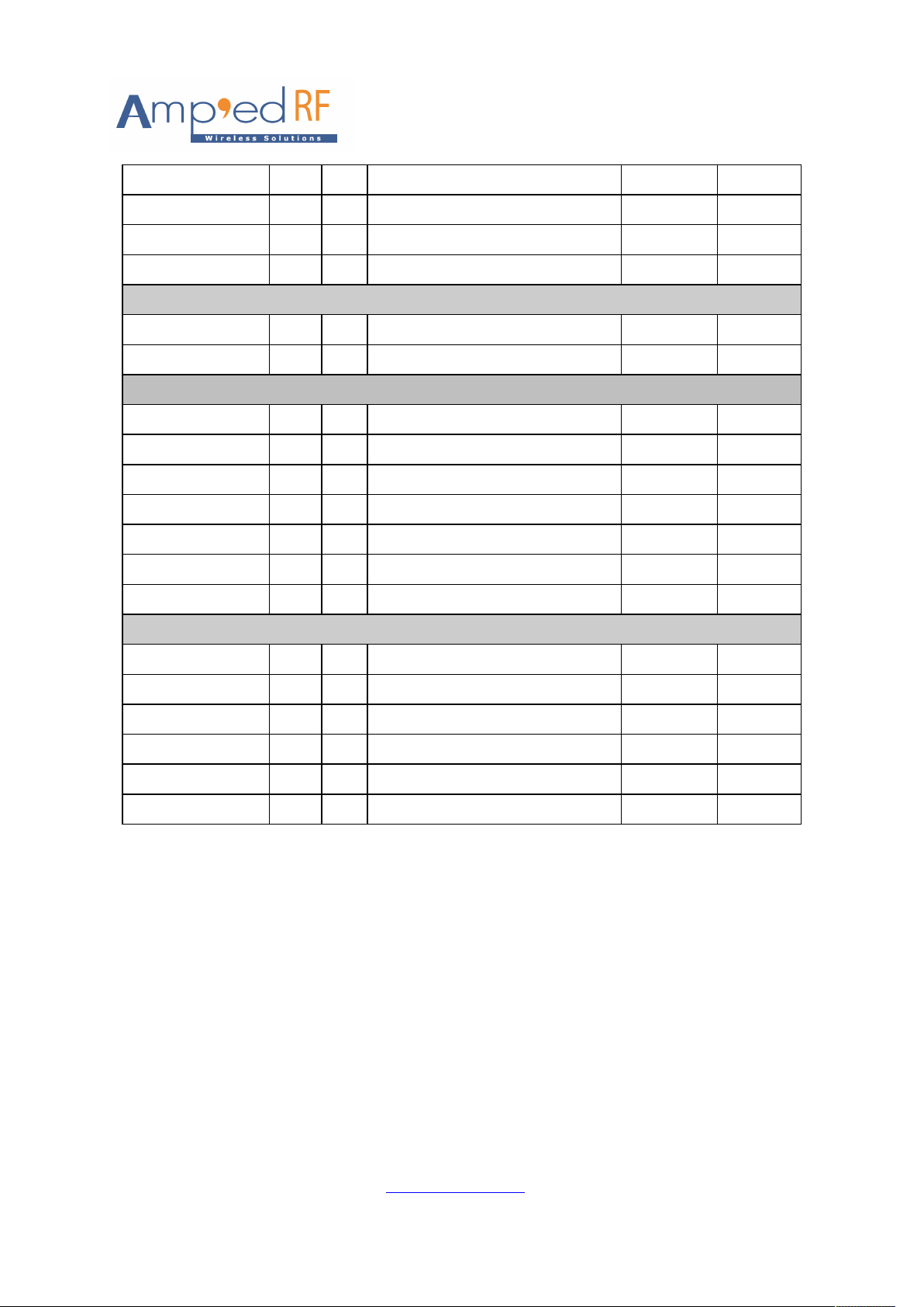
SDIO [3] I/O 15 SDIO DATA3 SPI CSN
SDIO [4] I/O 17 SDIO CLK SPI CLK
SDIO [5] I/O 14 SDIO DATA2 3.3v
SDIO INT I 8 SDIO external interrupt 1.8v
5GHz Interface
RF_IN_HB I 4 5GHz RF input
RF_OUT_HB O 5 5GHz RF output
External Antenna
GND 1 GND
WL_ANT 2 Antenna port for WIFI
GND 3 GND
GND 31 GND
BLE ANT 32 Antenna port for BLE
GND 33 GND
GND 36 GND
NC Pins
3.3v
3.3v
NC 25 Floating (Do not connect to ground)
NC 26 Floating (Do not connect to ground)
NC 27 Floating (Do not connect to ground)
NC 28 Floating (Do not connect to ground)
NC 30 Floating (Do not connect to ground)
NC 35 Floating (Do not connect to ground)
www.ampedrftech.com
9
Page 10
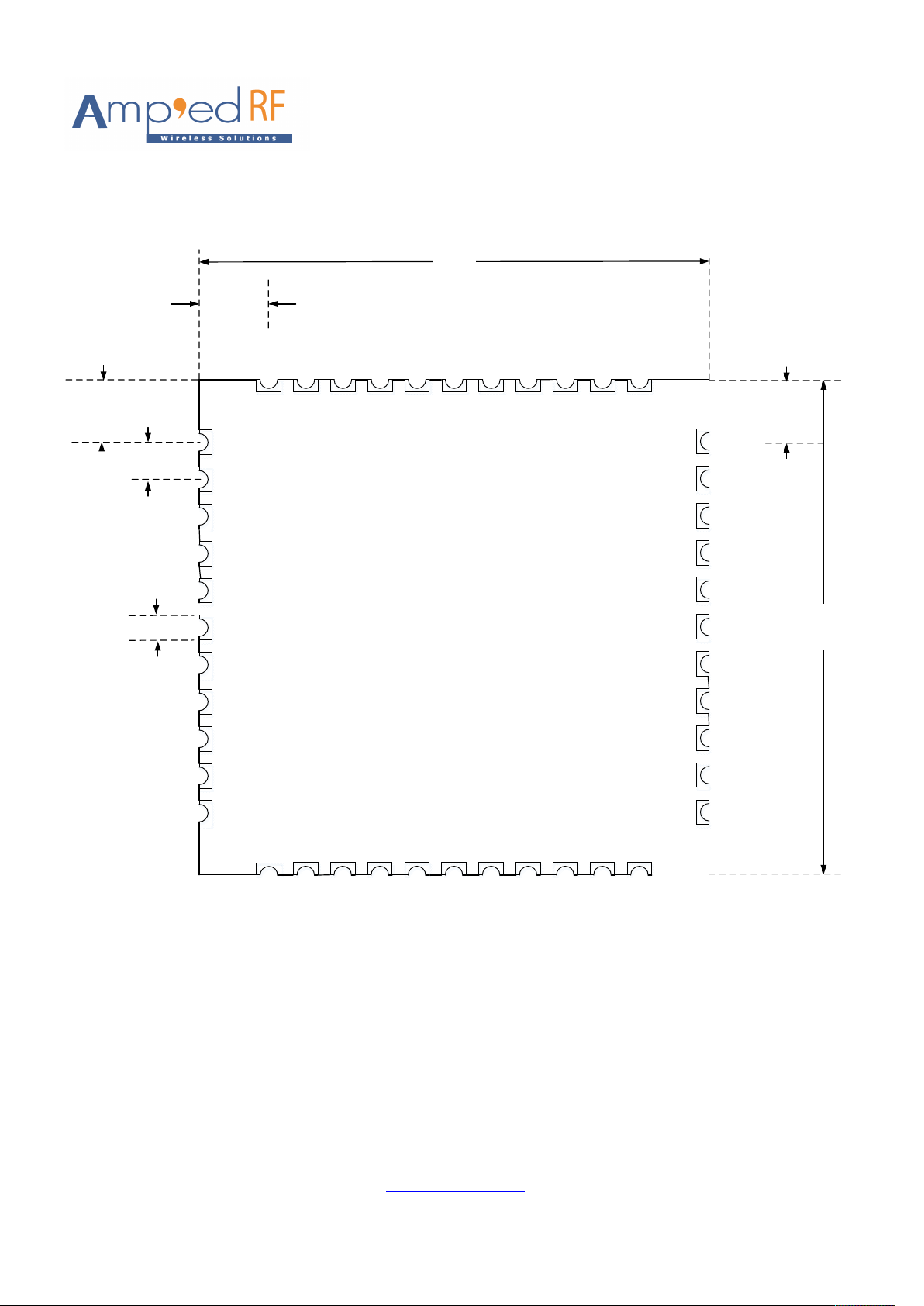
1.6. Layout Drawing ART6212
Size: 12 mm x 12mm x 2.4 mm (height)
59 mil
(1.5 mm)
472.4mil
(12 mm)
59 mil
(1.5 mm)
35.4 mil
(0.9 mm)
20 mil
(0.5 mm)
44 CTS
43 TXD
1 GND
2 Antenna port for WIFI
3 GND
4 RF_IN_HB
5 RF_OUT_HB
6 BT_WAKE
7 BT_HOST_WAKE
8 SDIO INT
9 VIN
10 26M XTAL_IN
59 mil
40 FEM_CTRL_2
41 RTS
42 RXD
38 32k XTAL_OUT
39 FEM_CTRL_1
36 GND
37 32k XTAL_IN
35 NC
34 BT_RST_N
(1.5 mm)
33 GND
32 Antenna port for BLE
31 GND
30 NC
TOP VIEW
29 VDD_1V8
28 NC
27 NC
26 NC
25 NC
24 LPO
472.4 mil
(12 mm)
11 26M XTAL_OUT
13 WL_HOST_WAKE
12 WL_REG_ON
16 SDIO CMD
15 SDIO DATA3
14 SDIO DATA2
17 SDIO CLK
18 SDIO DATA0
20 GND
19 SDIO DATA1
22 VDDIO
21 VIN_LDO_OUT
23 VIN_LDO
www.ampedrftech.com
10
Page 11

2. Hardware Design
All unused pins should be left floating; do not ground.
All GND pins must be well grounded.
Traces should not be routed underneath the module.
2.1. Module Reflow Installation
The ART6212 is a surface mount Bluetooth module supplied on a 44 pin, 6-layer PCB. The final assembly
recommended reflow profiles are:
For RoHS/Pb-free applications, Sn96.5/Ag3.0/Cu0.5 solder is recommended.
Maximum peak temperature of 230° - 240°C (below 250°C).
Maximum rise and fall slope after liquidous of < 2°C/second.
Maximum rise and fall slope after liquidous of < 3°C/second.
Maximum time at liquidous of 40 – 80 seconds.
www.ampedrftech.com
11
Page 12
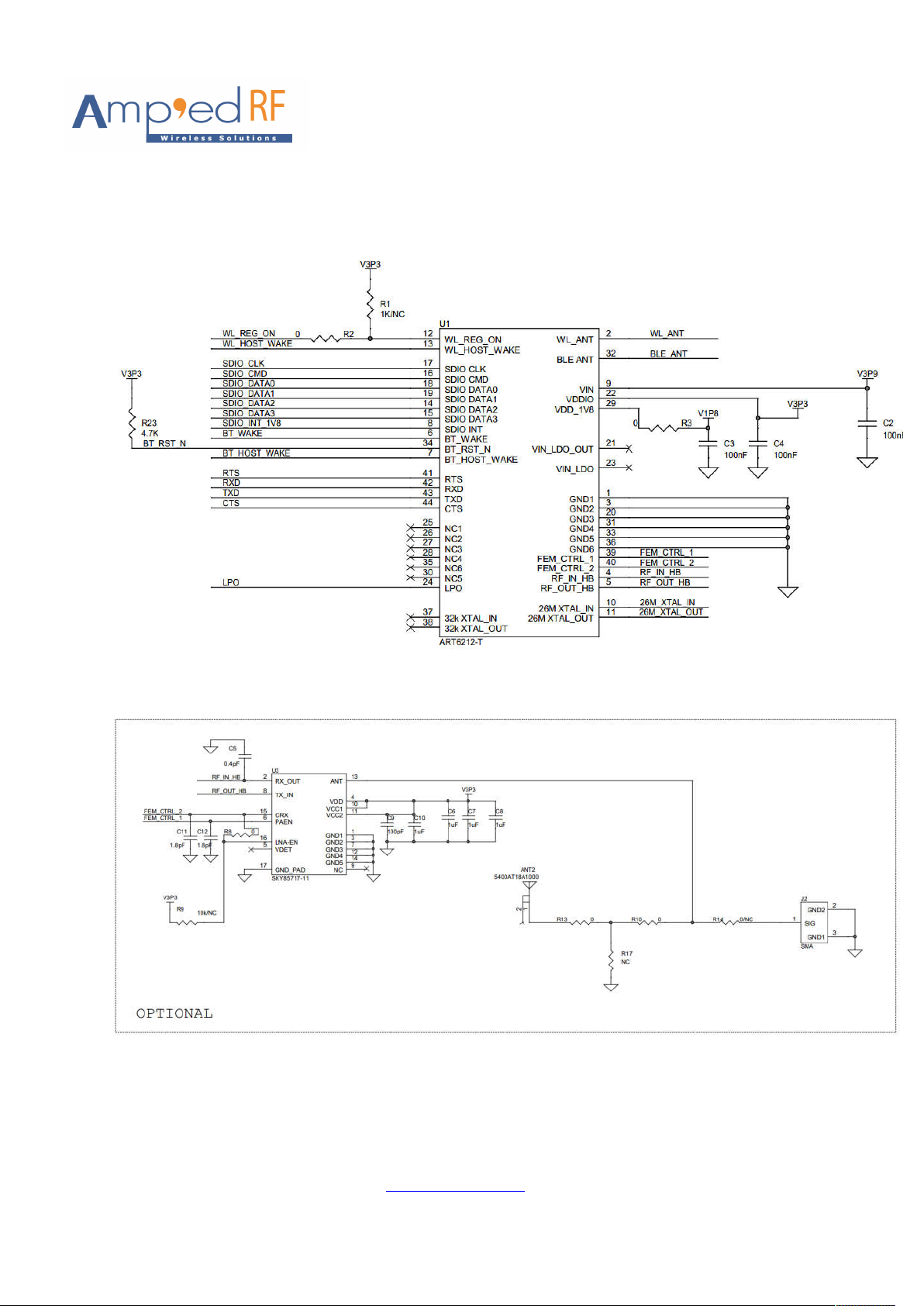
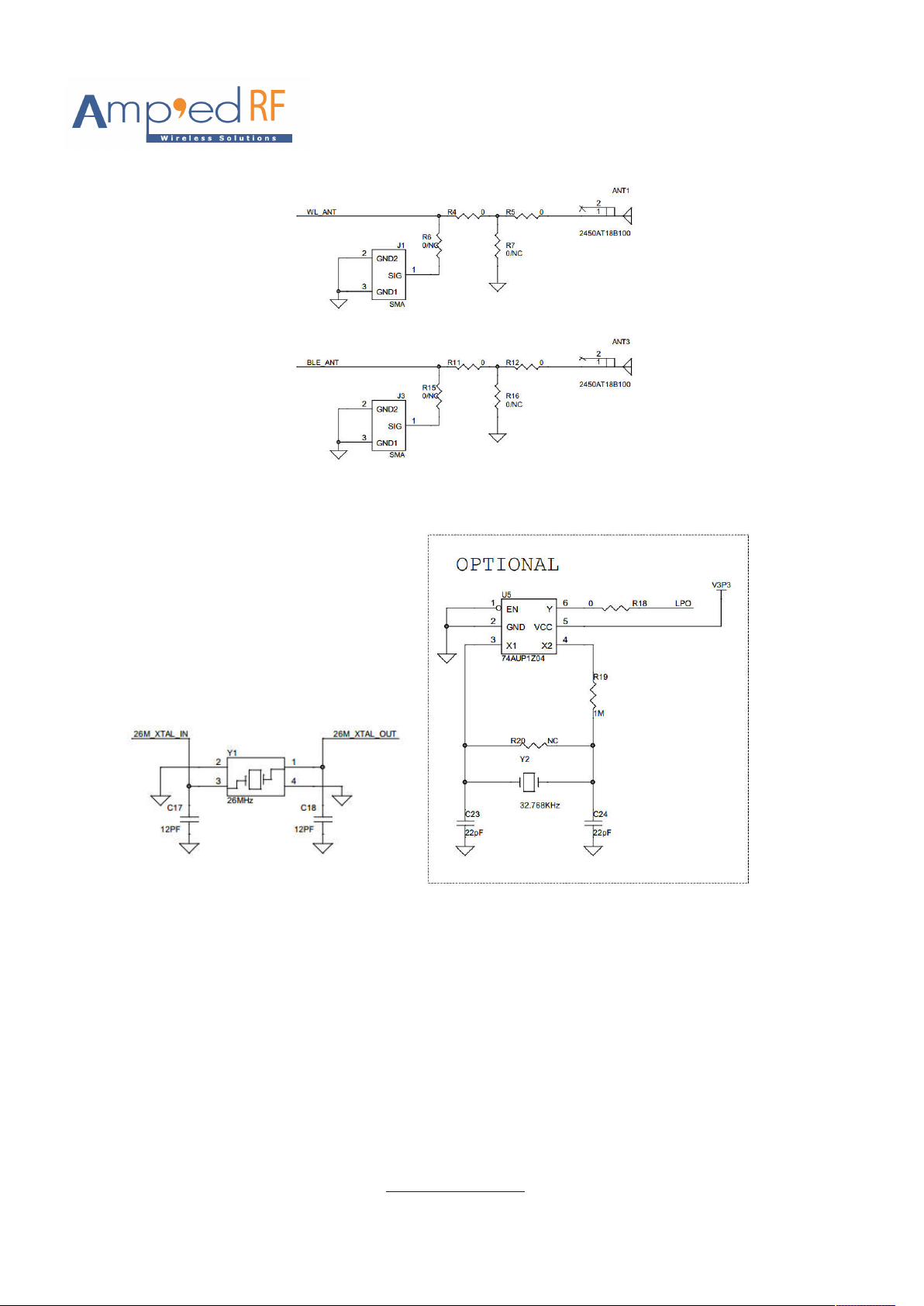
3. Reference Design Example ART6212
The follow circuits are examples of typical Linux based platform connections to the ART6212 module.
www.ampedrftech.com
12
Page 13
www.ampedrftech.com
13
Page 14
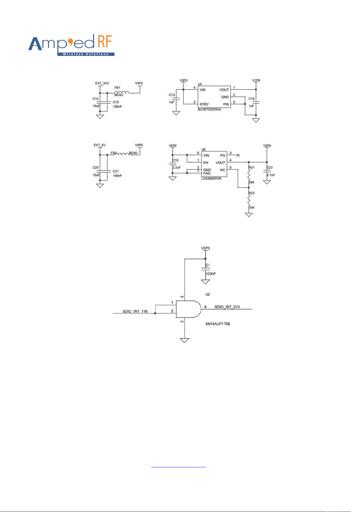
Note: It is better to use 9pF 26MHz crystal (Y1). The load capacitors (C17, C18) of crystal circuit is
recommended to be 12pF or 15pF which is depended the design of the PCB layout traces. The capacitors
ESR is better to be 0.1ohm at 100MHz. The traces from the crystal to the ART6212-T pads should be as
short as possible.
www.ampedrftech.com
14
Page 15
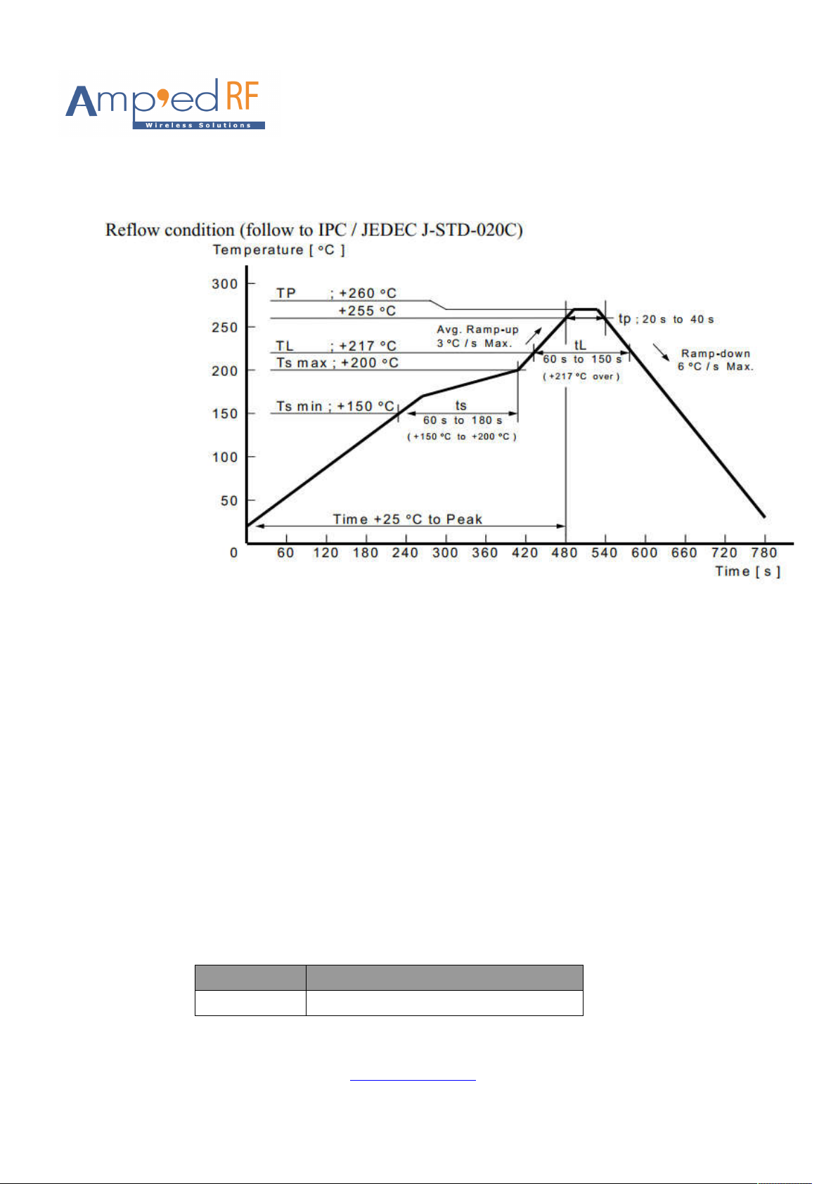
The recommended 26MHz crystal PN is Q22FA1280002000 and it’s soldered at the user’s PCB board by
the following condition:
4. Startup behavior
4.1. WL_REG_ON & BT_RST_N
These pins are always an input pins, active low, with a PD during reset. This signal MUST be active during
power supplies initialization and, when all power supplies are stable, it must remain active low for at least 2
cycles of the slow clock in order to insure good reset functionality.
When WL_REG_ON is low, the WIFI chip is power down.
When BT_RST_N is low, the WIFI chip is power down.
4.2. UART and SPI interface
UART_CTS is an input with PU, UART_RXD is an input with PU, UART_TXD toggles from input PU to output
High and UART_RTS toggles from input PU to output Low 70ms after reset, enabling UART communication
if needed.
5. RF Path Control
5.1. ART6212 Control
Version Path
ART6212-T WLAN 2.4GHz uses external ANT; BLE uses external
www.ampedrftech.com
15
Page 16
6. Ordering Information
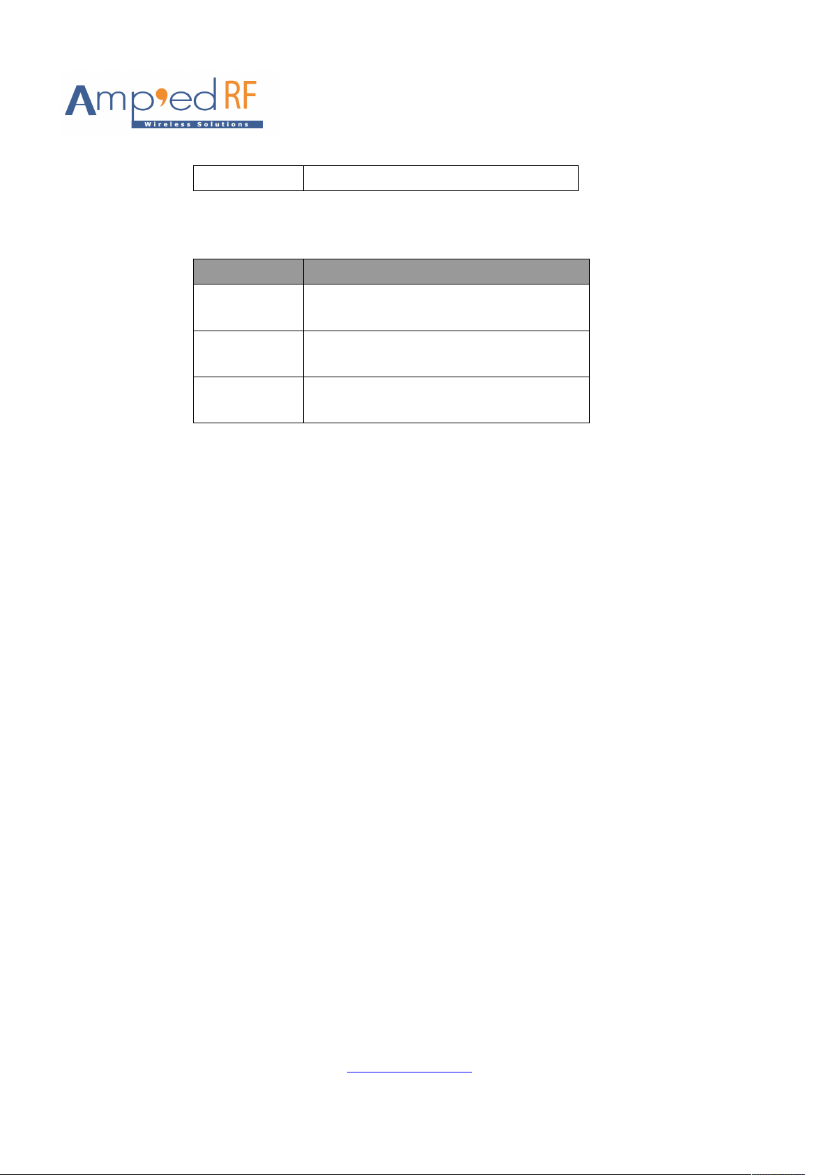
Part Name Description
ART6212-T-CM Combo WiFi and BLE.
ART6212-T-WF WiFi only
ART6212-T-BLE BLE only
ANT; WLAN 5GHz uses external antenna
External ant for WLAN/BLE 2.4GHz
External ant for WLAN
External ant for BLE
www.ampedrftech.com
16
Page 17
7. Warning
Please note that changes or modifications not expressly approved by the party responsible for compliance could void the user’s
authority to operate the equipment.
Note: This equipment has been tested and found to comply with the limits for a Class B digital device, pursuant to part 15 of the FCC
Rules. These limits are designed to provide reasonable protection against harmful interference in a residential installation. This
equipment generates uses and can radiate radio frequency energy and, if not installed and used in accordance with the instructions,
may cause harmful interference to radio communications. However, there is no guarantee that interference will not occur in a
particular installation. If this equipment does cause harmful interference to radio or television reception, which can be determined
by turning the equipment off and on, the user is encouraged to try to correct the interference by one or more of the following measures:
—Reorient or relocate the receiving antenna.
—Increase the separation between the equipment and receiver.
—Connect the equipment into an outlet on a circuit different from that to which the receiver is connected.
—Consult the dealer or an experienced radio/TV technician for help.
This equipment complies with radio frequency exposure limits set forth by the FCC for an uncontrolled environment.
This equipment should be installed and operated with a minimum distance of 20 cm between the device and the user or
bystanders.
This device must not be co-located or operating in conjunction with any other antenna or transmitter.
The user (OEM) must follow the datasheet instruction and Hardware guide. It is better to use the datasheet part3 reference
design.
The OEM
integrator must make the label (containing
ID X3ZWFMOD1) can
FCC
be seen by the operator.
Associated authorized antenna(s)
Authorized Antennas
Model Type Connector Antenna Gain
AT3216-B2R7HAA
AT3216-B5R5HAA
47950-1011
Surface Mount
Surface Mount Solder
PCB trace
Solder
U.FL
2.4GHz~2.483GHz:0.5dBi
4.9GHz ~ 5.85GHz
2.4GHz~2.483GHz:3dBi
8. Revision History
Date Revision Description
24 May 2016 0.1 Preliminary draft
2 Aug, 2016 1.0 Added BLE and WiFi only options to part number
29 Dec 2016 1.1 Change the UART TXD\RXD definition
20 Jan 2017 1.2 Added recommended crystal and load capacitors
: 2dBi
www.ampedrftech.com
17
 Loading...