


AMPAK
AP6XXX
Evaluation Kits
User manual
Version 1.2
Revision History
Date Revision Content Revised By Version
2012/12/26
2013/03/07
2013/06/06
AMPAK Technology Inc. www.ampak.com.tw Proprietary & Confidential Information i
Doc. NO:
Initial released Dora 1.0
Modify figure1 Dora 1.1
Modify figure1 Dora 1.2
1. AP6XXX Evaluation Board Introduction
AP6XXX Evaluation board (EVB) likes as figure1. That is designed for IEEE802.11
a/b/g/n/ac WLAN with integrated Bluetooth, FM, NFC and GPS application. It is subject
to provide a convenient environment for customer’s verification on WiFi or Bluetooth
function. There are many controller pins and reserved GPIO on Evaluation board which
describes as below.
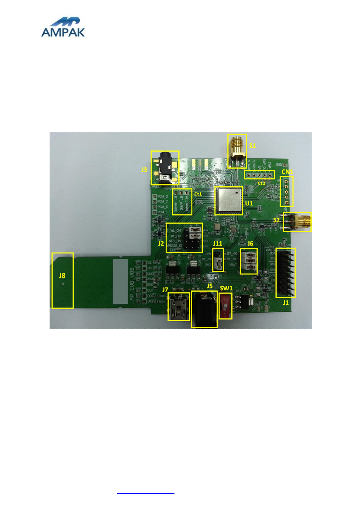
Figure1. Top view of AP6XXX EVB
Interface highlights:
1. U1: AP6XXX SIP module.
2. J1: UART interface connects with UART transport board for BT and GPS
measuring, it also provides I2C (SDA/SCL) for NFC measuring.
3. J2: Enable(H) or disable(L) Bluetooth, WiFi, NFC function and AP6335_SDIO I/O
voltage selection.(H for SDIO 3.3V, L for SDIO 1.8V)
4. J3: FM audio out interface.
5. J5: 5V DC adaptor input connector.
6. J6: VBAT / WL_VIO / BT_VIO for main system I/O power path.
7. J7: 5V DC mini USB input connector.
8. J8: Standard SDIO interfaces for Wi-Fi performance measured.
AMPAK Technology Inc. www.ampak.com.tw Proprietary & Confidential Information
Doc. NO:
1

9. J11: WL_VIO power path for 1V8 or 3V3 selection.
10. SW1: Power on/off switch.
11. CN1: NFC interface connects with NFC antenna.
12. S1: SMA connector let RF signal in/out path, you could connect with RF cable or
Dipole antenna.
13. S2: SMA connector let GPS RF signal input, you could connect with GPS
antenna.
14. Ct1: WLAN and BT control pins, strongly recommended WL_HWAKE(IRQ)
connected to MCU.
15. Ct2: NFC control pins, strongly recommended N_WAKE and N_H_WAKE
connected to MCU.
2. WiFi function verification step
WIFI SDIO: Using external pull up resistors depends on the SDIO supply voltage. For
1.8V, the resistance range is 30KΩ~82KΩ. For 3.3V, its range from 21
KΩ~41 KΩ on the four data lines and the CMD line as the following circuitry.
VIO_3V3
1 2
C10
10uF
R7 R10
SDIO_3V3
R28 R29
J8
SDCMD
SDCLK
Golden Finger_9
SD2
SD3
GND
3.3V
GND
SD0
SD1
9
1
2
3
4
5
6
7
8
SDIO_D 2
SDIO_D 3
SDIO_C MD
SDIO_C LK
SDIO_D 0
SDIO_D 1
R6
Figure2. WiFi verification connection interface to Host SDIO
Hardware Setup:
Refer to Figure2 SDIO pin definition connects the J8 interface of AP6XXX
evaluation board to Host SDIO control interface.
Using pull high resistors (R6, R7, R10, R28, R29) that resistance is 30Kohm for
1.8V or 3.3V VDDIO pull up voltage. (Pull high resistors are un-necessary if at
verification phase.)
Connects an external antenna at SMA connector on the evaluation board.
Note to the VDDIO voltage level should be the same with GPIO voltage level of
Host CPU. (VDDIO 3.3V or 1.8V selection by jump J11)
WiFi software setup:
Please follow up software guideline of Ampak official released.
AMPAK Technology Inc. www.ampak.com.tw Proprietary & Confidential Information
Doc. NO:
2

3. Bluetooth function verification step
Figure3. Bluetooth verification connection interface to Host UART
Hardware Setup:
Refer to Figure3 UART pin definition connects the J1 interface of AP6XXX
evaluation board to Host UART control interface.
Connects an external antenna at SMA connector on the evaluation board.
Note to the VDDIO voltage level should be the same as GPIO voltage level of
Host CPU.
WiFi and Bluetooth software setup:
Please follow up software guideline of Ampak official released.
AMPAK Technology Inc. www.ampak.com.tw Proprietary & Confidential Information
Doc. NO:
3

Federal Communications Commission (FCC) Statement
You are cautioned that changes or modifications not expressly approved by the part
responsible for compliance could void the user’s authority to operate the equipment.
This equipment has been tested and found to comply with the limits for a Class B digital
device, pursuant to part 15 of the FCC rules. These limits are designed to provide
reasonable protection against harmful interference in a residential installation. This
equipment generates, uses and can radiate radio frequency energy and, if not installed
and used in accordance with the instructions, may cause harmful interference to radio
communications. However, there is no guarantee that interference will not occur in a
particular installation. If this equipment does cause harmful interference to radio or
television reception, which can be determined by turning the equipment off and on, the
user is encouraged to try to correct the interference by one or more of the following
measures:
-Reorient or relocate the receiving antenna.
-Increase the separation between the equipment and receiver.
-Connect the equipment into an outlet on a circuit different from that to which the receiver is
connected.
-Consult the dealer or an experienced radio/TV technician for help.
This device complies with Part 15 of the FCC Rules. Operation is subject to the following
two conditions:
1) this device may not cause harmful interference, and
2) this device must accept any interference received, including interference that may
cause undesired operation of the device.
(WIFI) For product available in the USA/Canada market, only channel 1~11 can be
operated. Selection of other channels is not possible.
AMPAK Technology Inc. www.ampak.com.tw Proprietary & Confidential Information
Doc. NO:
4

FCC RF Radiation Exposure Statement :
1. This Transmitter must not be co-located or operating in conjunction with any other
antenna or transmitter.
2. This equipment complies with FCC RF radiation exposure limits set forth for an
uncontrolled environment. This equipment should be installed and operated with a minimum
distance of 20 centimeters between the radiator and your body.
This module has been granted modular approval for mobile applications. OEM integrators for
host products may use the module in their final products without additional FCC certification if
they meet the following conditions. Otherwise, additional FCC approvals must be obtained.
1. The host product with the module installed must be evaluated for simultaneous
transmission requirements.
2. The users manual for the host product must clearly indicate the operating requirements
and conditions that must be observed to ensure compliance with current FC RF exposure
guidelines.
3. To comply with FCC regulations limiting both maximum RF output power and human
exposure to RF radiation, the maximum antenna gain including cable loss in a mobile-only
exposure condition must not exceed {Insert Reference to Your Antenna Information Here.
Note: The end product shall has the words “Contains Transmitter Module FCC
ID: ZQ6-AP6212A”
AMPAK Technology Inc. www.ampak.com.tw Proprietary & Confidential Information
Doc. NO:
3
 Loading...