

Page 1

AMN11310
TM
WHDI
Transmitter
Module Datasheet
Version 0.4
Version 0.4
AMIMON Confidential i
Page 2

Important Notice
Important Notice
AMIMON Ltd. reserves the right to make corrections, modifications, enhancements, improvements, and other changes to its products
and services at any time and to discontinue any product or service without notice. Customers should obtain the latest relevant
information before placing orders and should verify that such information is current and complete. All products are sold subject to
AMIMON's terms and conditions of sale supplied at the time of order acknowledgment.
AMIMON warrants performance of its hardware products to the specifications applicable at the time of sale in accordance with
AMIMON's standard warranty. Testing and other quality control techniques are used to the extent AMIMON deems necessary to
support this warranty. Except where mandated by government requirements, testing of all parameters of each product is not
necessarily performed.
AMIMON assumes no liability for applications assistance or customer product design. Customers are responsible for their products
and applications using AMIMON components. To minimize the risks associated with customer products and applications, customers
should provide adequate design and operating safeguards.
AMIMON does not warrant or represent that any license, either express or implied, is granted under any AMIMON patent right,
copyright, mask work right, or other AMIMON intellectual property right relating to any combination, MAChine, or process in which
AMIMON products or services are used. Information published by AMIMON regarding third-party products or services does not
constitute a license from AMIMON to use such products or services or a warranty or endorsement thereof. Use of such information
may require a license from a third party under the patents or other intellectual property of the third party, or a license from AMIMON
under the patents or other intellectual property of AMIMON.
Reproduction of information in AMIMON data books or data sheets is permissible only if reproduction is without alteration and is
accompanied by all associated warranties, conditions, limitations, and notices. Reproduction of this information with alteration is an
unfair and deceptive business practice. AMIMON is not responsible or liable for such altered documentation.
Resale of AMIMON products or services with statements different from or beyond the parameters stated by AMIMON for that product
or service voids all express and any implied warranties for the associated AMIMON product or service and is an unfair and deceptive
business practice. AMIMON is not responsible or liable for any such statements.
All company and brand products and service names are trademarks or registered trademarks of their respective holders.
Contact Us
US Office
2350 Mission College Blvd.
Suite 500
Santa Clara, CA 95054
Tel: +1 650 641 7178
Israeli Headquarters
2 Maskit St.
Building D, 2nd Floor
P.O.Box 12618
Herzlia 46733, Israel
Tel: +972-9-962-9222
Fax: +972-9-956-5467
[email protected]
Japan Office
FS Building 9F.
1-14-9 Higashi-Gotanda Shinagawa-ku
Tokyo 141-0022,
Japan
TEL +81-3-3444-4305
[email protected]
Version 0.4
AMIMON Confidential ii
Page 3
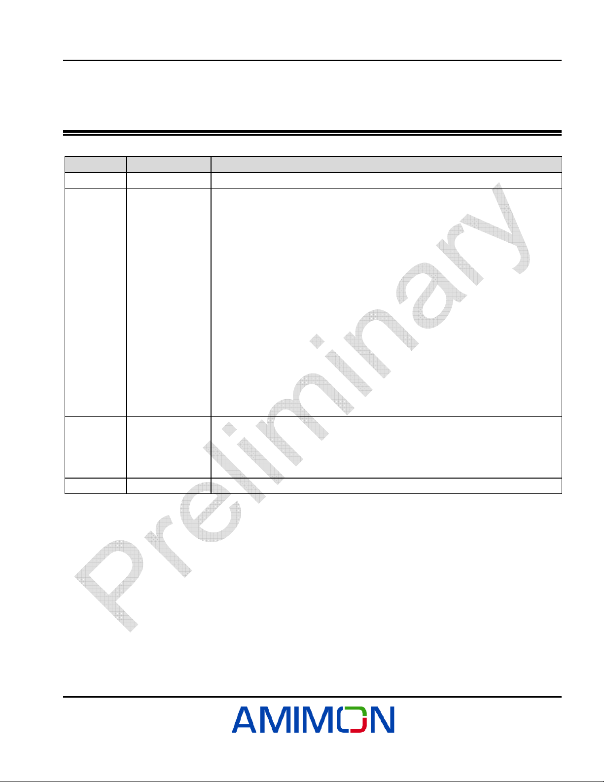
Revision History
Version Date Description
0.1 - Initial Release
0.2 15.6.08 Revision of RFIC board revB
Board Mechanical size
Reset and Wake-up Timer modified
RF frame modified
Power switch on RF removed
Operating Conditions and Electrical Characteristics modified
AMN11310 Block Diagram modified
Unhide Certification & Compliance
Power requirements
Mini-MAC changed to MAC
Add chapter RF AMN3110 Antenna diversity.
WHDI Module Configuration
Connector Schematics
Stack up
Test Points and Jumpers
0.3 20.7.08 Fixed link to STMF datasheet p-12.
Fixed pin id of WHDI connector p -25
Fixed recommended stack up table p- 23
Fixed power requirements p- 2
0.4 2.9.08 Change in FCC chapter
Revision History
Version 0.4
AMIMON Confidential iii
Page 4

Table of Contents
Table of Contents
List of Figures ......................................................................................................................................................... vi
List of Tables .......................................................................................................................................................... vi
Chapter 1, Introduction .............................................................................................. 1
1.1 Features......................................................................................................................................................... 1
Chapter 2, Overview ................................................................................................... 3
2.1 AMN2110 WHDI Baseband Transmitter...................................................................................................... 4
2.2 STM32F MAC µController ............................................................................................................................ 4
2.3 AMN3110 WHDITM 5GHz Transceiver ......................................................................................................... 5
2.4 Power Amplifier (PA) .................................................................................................................................... 5
2.5 Board Connector (WHDITM Connector)....................................................................................................... 5
2.6 Clocks ............................................................................................................................................................ 5
2.6.1 40MHz Crystal Oscillator.................................................................................................................. 5
2.6.2 40Mhz Digital Clock ......................................................................................................................... 5
2.6.3 10Mhz Micro Controller Clock .......................................................................................................... 5
2.7 RF AMN3110 Antenna Switching Switch ................................................................................................... 6
Chapter 3, Interfaces.................................................................................................. 7
3.1 Video Data Input and Conversions ............................................................................................................. 7
3.1.1 Video Channel Mapping ................................................................................................................... 8
3.1.2 Video Interface Input Timing Diagram ............................................................................................. 8
3.2 Audio Data Capture ...................................................................................................................................... 9
3.2.1 I2S Bus Specification ...................................................................................................................... 10
3.2.2 S/PDIF Bus..................................................................................................................................... 11
3.3 Management Buses and Connectors .......................................................................................................12
3.3.1 Two-Wire Serial Bus Interface ....................................................................................................... 12
3.3.2 Interrupts ........................................................................................................................................ 13
3.3.3 WHDI Module Configuration .......................................................................................................... 14
3.4 Reset and Wake-up Timer.......................................................................................................................... 14
Chapter 4, WHDI Connector Pins.............................................................................. 17
4.1 Signals ......................................................................................................................................................... 17
4.2 Connector Schematics............................................................................................................................... 18
4.3 Pin List......................................................................................................................................................... 19
Version 0.4
AMIMON Confidential iv
Page 5

Table of Contents
Chapter 5, Electrical Specifications ........................................................................ 21
5.1 Operating Conditions and Electrical Characteristics .............................................................................21
5.2 RF Characteristics TBD ............................................................................................................................. 22
Chapter 6, Design Guidelines ................................................................................... 23
6.1 Digital Layout Recommendation............................................................................................................... 23
6.1.1 Stack up ......................................................................................................................................... 23
6.1.2 General Guidelines ........................................................................................................................ 24
6.1.3 WHDI Lines .................................................................................................................................... 24
6.1.4 Power and Ground ......................................................................................................................... 24
6.2 RF Design Recommendation..................................................................................................................... 24
6.2.1 RF Components ............................................................................................................................. 24
6.2.2 Power Management ....................................................................................................................... 24
6.3 Test Points and Jumpers ........................................................................................................................... 25
Chapter 7, Mechanical Dimensions.......................................................................... 27
7.1 RF Shield Frame and Cover....................................................................................................................... 29
Version 0.4
AMIMON Confidential v
Page 6

List of Figures
List of Figures
Figure 1: AMN11310 Block Diagram......................................................................................................................... 3
Figure 2: WHDI Baseband Transmitter Chipset ........................................................................................................ 4
Figure 3: Video Data Processing Path ...................................................................................................................... 7
Figure 4: Timing Diagram .......................................................................................................................................... 9
Figure 5: I2S Simple System Configurations and Basic Interface Timing ............................................................... 10
Figure 6: I2S Input Timings ...................................................................................................................................... 11
Figure 7: Two-Wire Application/MAC Connection ................................................................................................... 12
Figure 8: Two-Wire MAC Write Commands ............................................................................................................ 13
Figure 9: Two-Wire Read Command....................................................................................................................... 13
Figure 10: Reset Time Diagram .............................................................................................................................. 14
Figure 11: Reset Mechanism .................................................................................................................................. 15
Figure 12: WHDI Connector .................................................................................................................................... 18
Figure 13: Mechanical Dimensions Top View ......................................................................................................... 27
Figure 14: Mechanical Dimensions Bottom View .................................................................................................... 28
Figure 15: RF-Shield Frame .................................................................................................................................... 29
Figure 16: RF-Shield Cover..................................................................................................................................... 30
List of Tables
Table 1: Common Supported Video Input Resolutions ............................................................................................. 8
Table 2: Video Channel Mapping .............................................................................................................................. 8
Table 3: Video Interface ............................................................................................................................................ 8
Table 4: I2S Audio Interface Timing Requirements ................................................................................................10
Table 5: Audio Interface Timing Requirements ....................................................................................................... 11
Table 6: Device Addresses ..................................................................................................................................... 12
Table 7: Reset Timing Requirements...................................................................................................................... 15
Table 8: WHDI Connector Signals .......................................................................................................................... 17
Table 9: Tx WHDI Connector Pin List ..................................................................................................................... 19
Table 10: Absolute Maximum Ratings over Operating Case Temperature Range................................................. 21
Table 11: Recommended Operating Conditions ..................................................................................................... 21
Table 12: Electrical Characteristics over Recommended Range of Supply Voltage and Operating Conditions .... 21
Table 13: Digital Layout Recommendation ............................................................................................................. 23
Version 0.4
AMIMON Confidential vi
Page 7

Introduction
Chapter 1
Introduction
The AMN11310 is the second generation of WHDITM transmitter board. It is based on AMIMON's WHDI
transmitter chipset: the AMN2110 baseband transmitter and the AMN3110 RFIC transmitter.
The AMN11310 WHDITM wireless transmitter module, together with the AMN12310 wireless receiver module,
presents the ultimate solution for converting any High Definition (HD) system into a wireless one. These add-on
modules enable wireless A/V applications that easily fit into the living room and eliminate traditional A/V wiring.
The perfect HD video and audio quality and the high robustness are unmatched by any other wireless technology,
and present a true alternative to cable. The WHDI system transmits uncompressed video and audio streams
wirelessly and thus simplifies and eliminates system issues such as lip-sync, large buffers and other burdens like
retransmissions or error propagation.
1.1 Features
• Uncompressed and uncompromised HD video quality, using AMIMON's baseband chipsets:
AMN2110: WHDITM Baseband Transmitter
AMN3110: WHDITM RFIC Transmitter
• WHDI – Wireless High Definition Interface:
Digital video: 30-bit RGB or YCrCb
Digital audio: I2S and SPDIF
Two-Wire serial bus slave interface
One interrupt line
• Supports any uncompressed video resolutions, including:
HD: 720p, 1080i, 1080p, 576i, 576p, 480p, 480i
PC: VGA (640x480), SVGA (800x600), XGA (1024x768)
Panel: 854x800, 1280x768, 1366x768
• Audio:
Up to 3Mbps audio stream:
I2S: Two PCM channels (sampled up to 48 KHz x 24 bit)
SPDIF: Including AC-3, DTS
• Strong 256-bit AES encryption
• User-defined two-way channel with minimum 10 Kbps for data and control
• Less than 1mSec latency between source and sink
• Small mechanical footprint:
PCB integrated antennas
Version 0.4
AMIMON Confidential 1
Page 8

Introduction
• RF characteristics:
MIMO technology, using 5GHz unlicensed band, 18MHz bandwidth.
Coexists with 802.11a/n and 5.8GHz cordless devices.
Support for Automatic Transmission Power Control (ATPC).
No line of sight needed between transmitter and receiver. It has a range of over 30 meters, suitable for
almost any room.
14mW typical transmission power per transmitting channel.
Maximum 20mW transmission power per transmitting channel.
Uplink antenna switching
• Current consumption
Option to disable 40MHz digital clock to AMN2110 from AMN3110.
• Power requirements:
3.3V (±5%), ~6.2 W
• Certification & Compliance:
FCC
This product is for indoor use only in the band of 5.15-5.25GHz.
AMN11310 complies with part 15 of the FCC Rules. Operation is subject to the following two
conditions: (1) This device may not cause harmful interference, and (2) this device must accept any
interference received, including interference that may cause undesired operation.
Any changes or modifications not expressly approved by Amimon for compliance could void the user's
authority to operate the equipment.
This equipment has been tested and found to comply with the limits for a Class B digital device,
pursuant to part 15 of the FCC Rules. These limits are designed to provide reasonable protection
against harmful interference in a residential installation. This equipment generates uses and can
radiate radio frequency energy and, if not installed and used in accordance with the instructions, may
cause harmful interference to radio communications. However, there is no guarantee that interference
will not occur in a particular installation. If this equipment does cause harmful interference to radio or
television reception, which can be determined by turning the equipment off and on, the user is
encouraged to try to correct the interference by one or more of the following measures:
Reorient or relocate the receiving antenna.
Increase the separation between the equipment and receiver.
Connect the equipment into an outlet on a circuit different from that to which the receiver is
connected.
Consult the dealer or an experienced radio/TV technician for help.
MIC
This device complies with Japan Radio Law:
Item 19-11 of Article 1, paragraph 1, of certification ordinance.
Item 19-3 of Article 1, paragraph 1, of certification ordinance.
• Caution: The module should be positioned so that personnel in the area for prolonged periods may safely
remain at least 20 cm (8 in) in an uncontrolled environment from the module.
Version 0.4
AMIMON Confidential 2
Page 9
Overview
Chapter 2
Overview
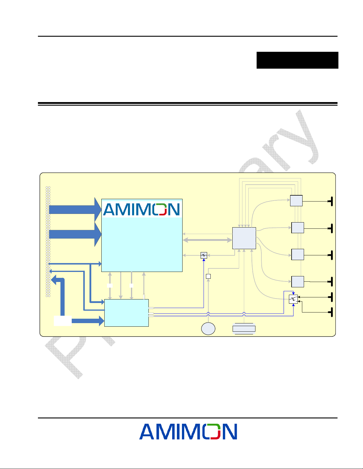
The AMN11310 WHDI Video Source Unit (VSU) is designed to modulate and transmit downstream video and
audio content over the wireless medium and receive a control channel over the wireless upstream. The
modulation uses 18MHz bandwidth and is carried over the 5GHz unlicensed band. Figure 1 displays a block
diagram of the AMN11310. The inputs to the VSU are digital uncompressed video, digital audio and control, all
via the WHDI connector. It has a MIMO design of four wireless output channels and a slow rate data input
wireless channel. The MAC uC is responsible for the control and the management.
PA_DET_1
PA_DET_2
PA_DET_3
PA_DET_4
PA
VIDEO
Connector
TH
80 Pin WHDI
WHDI_RESET_
(reset from whdi)
WHDI_INT
(interrupt from whdi)
Control
TwoWire
Audio
WHDI_SDA
WHDI_SCL
AMN2110
WHDITM Baseband Transmitter
S_RESET_B
Int
PIN#61
PIN#15
PIN#58
PIN#59
SPI
UC_MAC_CLK
(Clock 10MHz)
uC
MAC
Figure 1: AMN11310 Block Diagram
Clk40M_OE
ANT_CON_P
ANT_CON_N
CLK40M
RSSI_DET
clken
3.3V
DIG_CLK (40M)
3.3V_RAIL
fb
3.3V
PA
AMN3110
PA
(Clock 40MHz)
PA
40M XTAL
Version 0.4
AMIMON Confidential 3
Page 10
Overview
The main building blocks of the AMN11310 are as follows:
• AMN2110 WHDI Baseband Transmitter, as briefly described on page 4.
• STM32F MAC µController, as briefly described on page 4.
• AMN3110 WHDITM 5GHz Transceiver, as briefly described on page 5.
• Power Amplifier (PA), as briefly described on page 5.
• Board Connector (WHDITM Connector), as described on page 5.
• 40MHz Crystal Oscillator, as described on page 5.
• RF AMN3110 Antenna Switching Switch, as described on page 6.
2.1 AMN2110 WHDI Baseband Transmitter
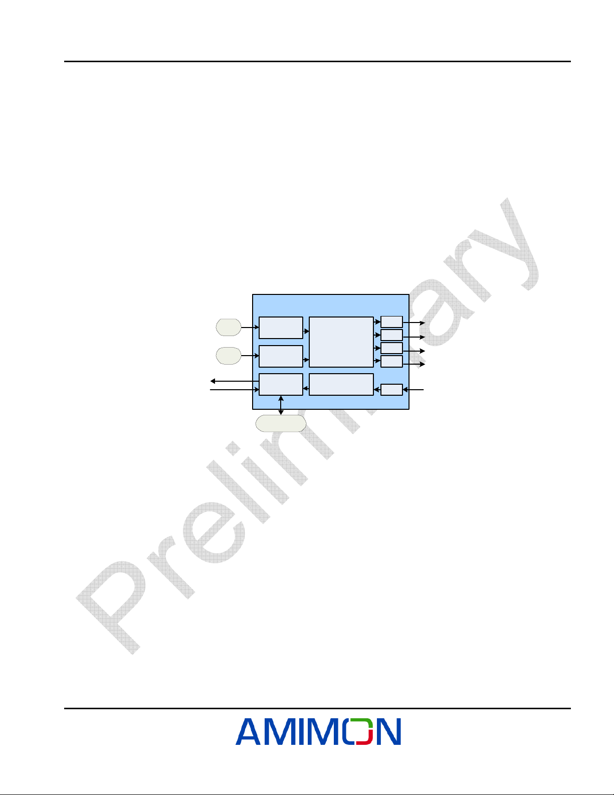
The AMN2110 WHDITM baseband transmitter chip is the heart of the AMN11310 WHDI transmitter module. The
AMN2110 interfaces the A/V source through the WHDI connector, and is controlled on board by the MAC uC.
WHDITM Baseband Transmitter
Video
Source
Audio
Source
Video
Interface
Audio
Interface
Control
MiniMAC
MicroController
Downlink
Modulation
Uplink
De-modulation
AMN2110
DAC
DAC
DAC
DAC
ADC
Figure 2: WHDI Baseband Transmitter Chipset
The AMN2110 is based on MIMO technology transmitting through up to four output channels. Four
digital-to-analog converters and one analog-to-digital converter are embedded within the chip.
The AMN2110 internal PLL accepts an input clock frequency of 40MHz. The input frequency is multiplied and
then used as an internal system clock.
2.2 STM32F MAC µController
The STM32F Microcontroller is based on an ARM 32-bit Cortex™-M3 CPU, with 128 Kbytes of embedded Flash
memory. It is used as an external microcontroller for implementing the MAC layer of the WHDI link.
The STM32F Internal PLL accepts an input clock frequency of 10MHz and generates an internal 60MHz system
clock. The STM32F also has an option to work with an internal 4-to-16 MHz oscillator.
Version 0.4
AMIMON Confidential 4
Page 11

Overview
2.3 AMN3110 WHDITM 5GHz Transceiver
The VSU uses the AMN3110 chip. The AMN3110 is a fully integrated direct conversion MIMO transmitter
specifically designed for WHDI applications using OFDM modulation in single-band 4.9GHz to 5.9GHz. The
device includes:
• Four Complete Downlink Direct Conversion Transmitters
• One Uplink Receiver
• Integrated Synthesizer
• Internal DC Servo Loops
• RSSI
• IQ Detector
• RF and Baseband Control Interface
• Power Management Unit
• 3-Wire SPI Interface
To complete RF front-end solution, the AMN3110 uses external PA, RF switches, RF Band Pass Filters (BPF),
RF BALUNs and a few passive components.
2.4 Power Amplifier (PA)
In order to extend the operating range for the AMN11310, the RF transmitter uses power amplifiers. Each power
amplifier has an output power detector for TPC purposes.
AMN11310 uses Sharp IRM053U7 PAs.
2.5 Board Connector (WHDITM Connector)
For information regarding the connector specification and pin-outs, see section Signals, page 17.
2.6 Clocks
2.6.1 40MHz Crystal Oscillator
An on-board 40MHz Oscillator is connected to the AMN3110 chip.
2.6.2 40Mhz Digital Clock
AMN3110 drives the 40MHz clock to the baseband AMN2110 through a buffer (with output enable).
This clock is named DIG_CLK. The control to the output buffer is named Clk40M_OE.
2.6.3 10Mhz Micro Controller Clock
The DIG_CLK (40MHz) clock is divided by four by the AMN2110 and generates 10MHz that drives the STM32F
UC.
Version 0.4
AMIMON Confidential 5
Page 12

Overview
2.7 RF AMN3110 Antenna Switching Switch
The antenna switching switch controls two input options: reception from on board printed antenna or SPIFA
(standing antenna) for uplink channel. This switch is controlled by two general purpose pins of the STM32F UC:
GPIO PB6 pin#58 and PB7 pin#59.
Version 0.4
AMIMON Confidential 6
Page 13
3.1 Video Data Input and Conversions
Interfaces
Chapter 3
Interfaces
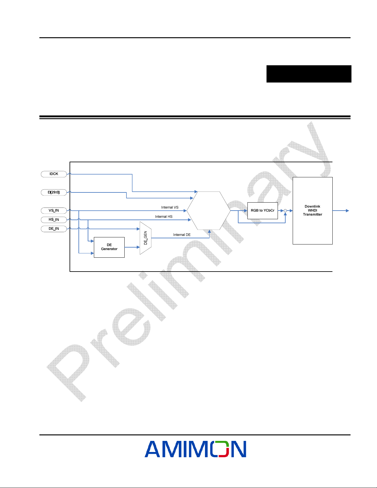
Figure 3: Video Data Processing Path
Figure 3 shows the stages for processing video data through the AMN2110. The HSYNC and the VSYNC input
signals are mandatory. The DE input signal is optional and can be created with the DE generator using the
HSYNC and the VSYNC pulses.
The video input data is uncompressed digital video up to 3*10 bits in width.
Important: When connected to a 3*8 bits source, connect the appropriate LSBs to GND.
The video interface provides a direct connection to the outputs from an HDMI receiver or from an MPEG decoder.
The appropriate registers must be configured to describe which format of video to input into the AMN11310. Refer
to the appropriate programmer's reference guide for more details.
DATA Enable (DE) Generator
The AMN2110 includes logic to construct the DE signal from the incoming HSYNC, VSYNC and clock. Registers
are programmed to enable the DE signal to define the size of the active display region.
Version 0.4
AMIMON Confidential 7
Page 14
Interfaces
Color Space Converter
The AMN11310 can receive either RGB or YCbCr color space. For more details, you may refer to the MAC
registers in the programmer's reference guide.
Common Video Input Format
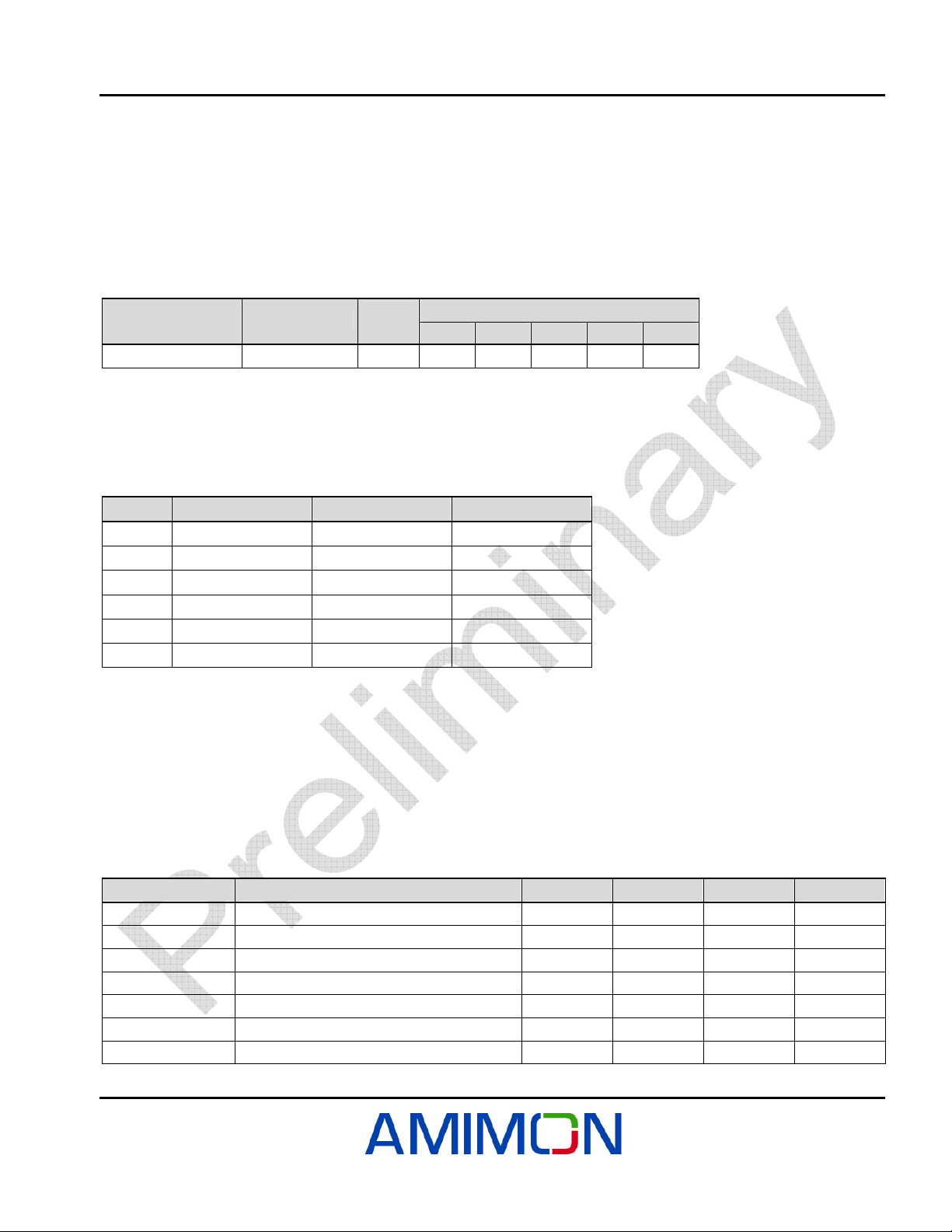
Table 1 describes the common supported video input resolutions.
Table 1: Common Supported Video Input Resolutions
Color Space Video Format
RGB/YCbCr 4:4:4 24 27 27 65 74.25 74.25
Bus
Width
480i 480p XGA 720p 1080i
Input Pixel Clock (MHz)
3.1.1 Video Channel Mapping
The 30 bit video input signals are mapped to the RGB and YCbCr color space according to the options described
in the following table:
Table 2: Video Channel Mapping
Option D[29:20] D[19:10] D[9:0]
#1 RED (Cr) GREEN (Y) BLUE (Cb)
#2 RED (Cr) BLUE (Cb) GREEN (Y)
#3 GREEN (Y) RED (Cr) BLUE (Cb)
#4 GREEN (Y) BLUE (Cb) RED (Cr)
#5 BLUE (Cb) RED (Cr) GREEN (Y)
#6 BLUE (Cb) GREEN (Y) RED (Cr)
The AMN11310 allows any of the input video channels options. The first option is the default from power-up. In
order to change the video channel mapping, please refer to the appropriate programmer's reference guide.
3.1.2 Video Interface Input Timing Diagram
3.1.2.1 Timing Requirements
Important: The following parameters relate to the AMN2110 baseband chipset and not to the entire AMN11310
board.
Table 3: Video Interface
Symbol Parameter MIN TYP MAX Units
TDCKCYC DCLK period 12.5 74.1 ns
TDCKFREQ DCLK frequency 13.5 80 MHz
TDCKDUTY DCLK duty cycle 40% 60% ns
TDCKSUR Setup time to DCLK rising edge 0.7 ns
TDCKHDR Hold time to DCLK rising edge 1.1 ns
TDCKSUF Setup time to DCLK falling edge 1.5 ns
TDCKHDF Hold time to DCLK falling edge 0.5 ns
Version 0.4
AMIMON Confidential 8
Page 15
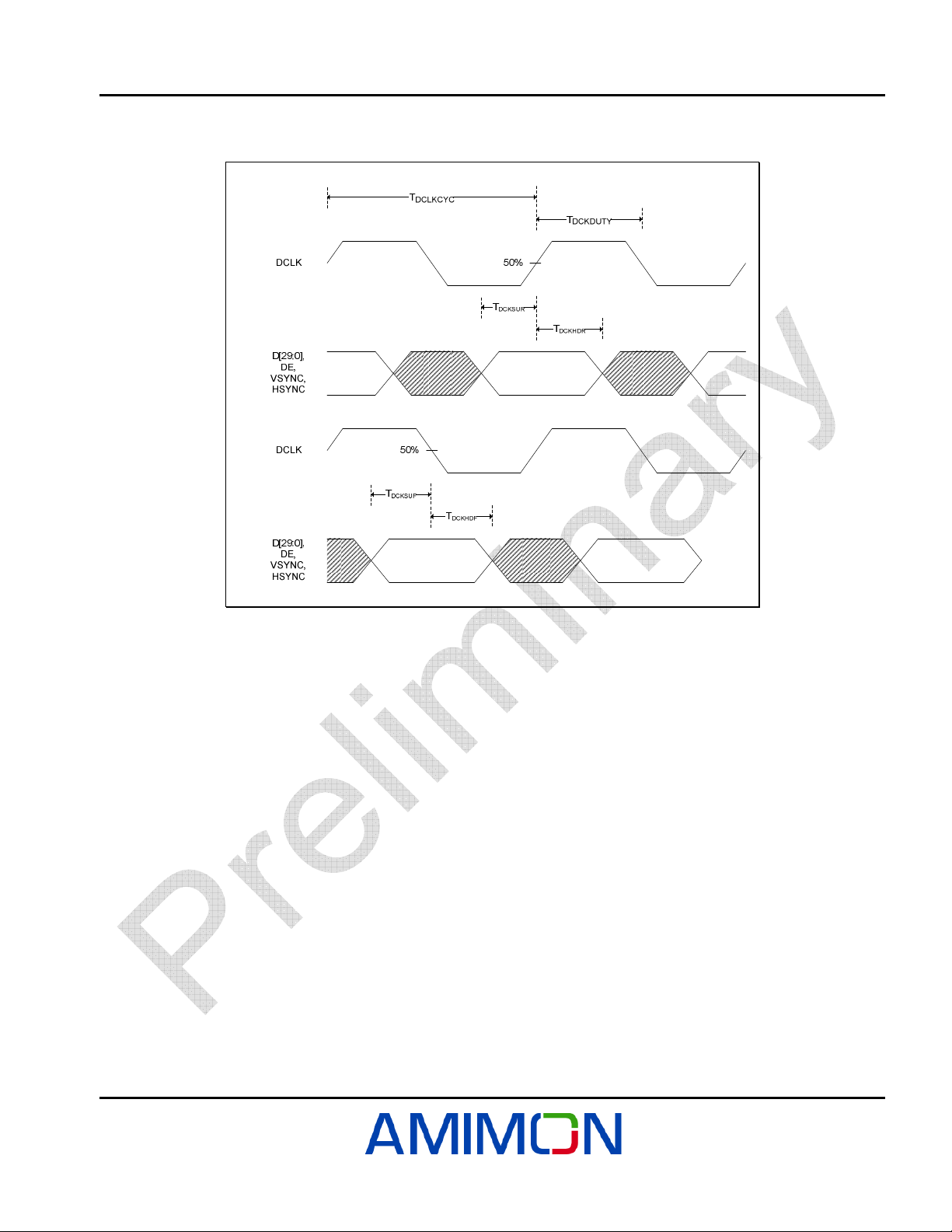
3.1.2.2 Timing Diagram
EDGE = 0 EDGE = 1
Interfaces
Figure 4: Timing Diagram
3.2 Audio Data Capture
AMN11310 transports an explicit audio master clock with appropriate data-over-the-wireless link. No constraints
exist for a coherent video and audio clock, where coherent means that the audio and the video clock must have
been created from the same clock source. The AMN11310 can accept digital audio from either SPDIF or I2S
inputs.
The AMN11310 supports two channel audio sampling frequencies of up to 48KHz and of up to 32 bits per sample
(For I2S – only 24 bits are supported).
Version 0.4
AMIMON Confidential 9
Page 16
Interfaces
3.2.1 I2S Bus Specification
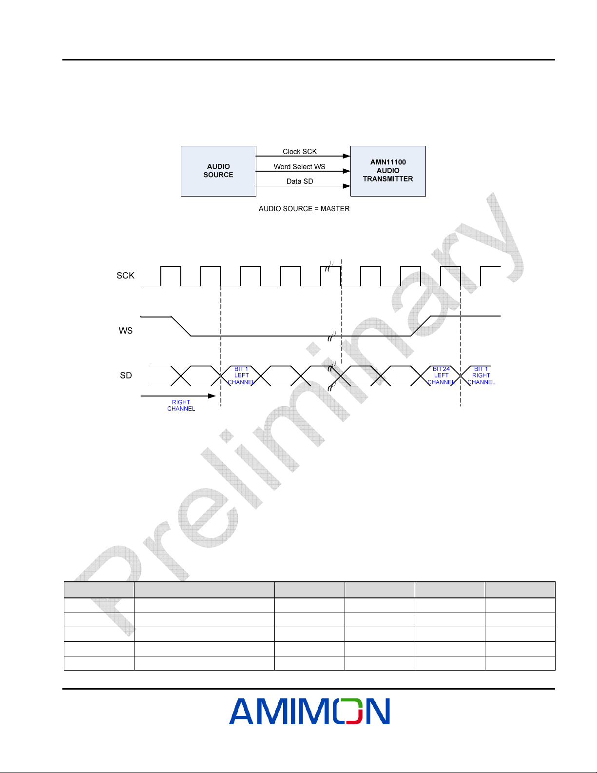
The AMN11310 supports a standardized communication structure inter-IC sound (I2S) bus. As shown in Figure 5,
the bus has three lines: continuous serial clock (SCK), word select (WS) and serial data (SD). The external
device generating SCK and WS is the audio source.
Figure 5: I2S Simple System Configurations and Basic Interface Timing
The AMN11310 supports an I2S format of up to 32 bits for each channel (left and right). The serial data is latched
into the AMN11310 on the leading (LOW to HIGH) edge of the clock signal. The WS is also latched on the
leading edge of the clock signal. The WS line should change one clock period before the first bit of the channel is
transmitted.
The AMN11310 transmits explicit clock SD and WS and does not process the audio content. The input audio at
the transmitter end is mirrored to the receiver end. The source may have different word lengths, up to 32 bits.
However, the AMN11310 always samples and transmits 24 bits over the wireless link.
3.2.1.1 Timing Requirements
Table 4: I2S Audio Interface Timing Requirements
Symbol Parameter MIN TYP MAX Units
TSCKCYC SCK period 325 976 ns
TSCKFREQ SCK frequency 1.024 3.072 MHz
TSCKDUTY SCK duty cycle 40 60 %
TDCKSETUP Setup time to SCK rising edge 25 ns
TDCKHOLD Hold time to SCK rising edge 25 ns
Version 0.4
AMIMON Confidential 10
Page 17
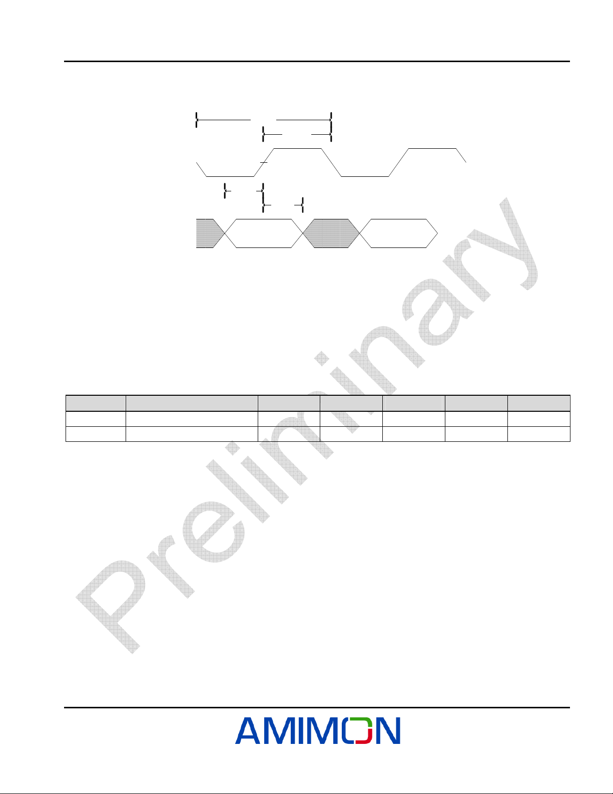
3.2.1.2 Timing Diagram
Interfaces
SCK
SD,WS
T
DCKSETUP
50%
T
SCKCYC
T
DCKH OLD
T
SCKDUTY
Figure 6: I2S Input Timings
3.2.2 S/PDIF Bus
3.2.2.1 Timing Requirements
The AMN11310 does not require the SPDIF clock. The clock is produced internally by sampling the SPDIF data
input at a high clock rate and processing it.
Table 5: Audio Interface Timing Requirements
Symbol Parameter Condition MIN TYP MAX Units
TSPCYC SPDIF data sampling rate 162 488 ns
TSPFREQ SPDIF data sampling freq 2.048 6.144 MHz
Version 0.4
AMIMON Confidential 11
Page 18
Interfaces
3.3 Management Buses and Connectors
3.3.1 Two-Wire Serial Bus Interface
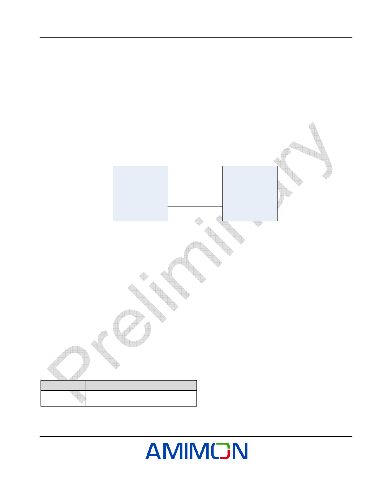
The WHDI application observes and controls the AMN11310 via a Two-Wire interface and an interrupt line
connecting the application microcontroller and the AMN11310 MAC microcontroller. The protocol of the Two-Wire
bus for the WHDI application/MAC interface is described in the following sections.
The Two-Wire bus is bidirectional and, as its name implies, has only two wires: a Serial Clock Line (SCL) and a
Serial Data Line (SDA). The Two-Wire architecture includes master and slave devices. The master initiates a
data transfer on the bus and generates the clock signal. The AMN11310 MAC operates as a slave device. Each
slave device is recognized by a unique address and can operate as either a receive-only device or a transmitter
with the ability to both receive and send information.
SDA
Application
MicroController
(Two-Wire Master)
SCL
WHDI MAC
(Two-Wire Slave)
Figure 7: Two-Wire Application/MAC Connection
On top of the Two-Wire low level operation described in sections 3.3.1.3 and 3.3.1.4, the WHDI application and
the MAC microcontrollers communicate with each other in a defined protocol, which avoids all possibilities of
confusion. The protocol defines command oriented transactions between the application and the WHDI MAC.
Each Two-Wire command has a predefined data byte length and is defined to be exactly one Two-Wire
transaction long.
3.3.1.1 Two-Wire Timing
Generally, the clock frequency of the bus is dictated by the slowest device on the Two-Wire interface. However,
the selected MAC supports the 100 KHz SCL frequency rate.
Refer to STM32F Two-wire reference application note for detailed description of the physical protocol and timing.
http://www.st.com/stonline/products/literature/ds/13587.pdf, pp 55-59.
3.3.1.2 Device Addresses
The MAC device address may be altered by two jumpers on VDU/VSU board.
Table 6: Device Addresses
Device Address
MAC uC 0x62 or 0x82 or 0x90 or 0x70
(Board configuration dependant)
Alternatively, the device address can be set in the MAC SW in advance.
Version 0.4
AMIMON Confidential 12
Page 19
Interfaces
3.3.1.3 MAC uC Write Operation
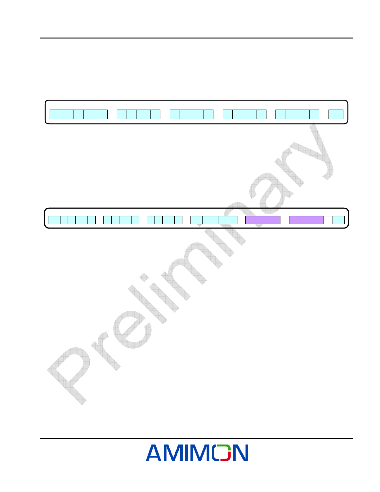
Figure 8 demonstrates a write transaction which sends 2 data bytes and which ends with the master stop bit.
Each write transaction sends 1 or more data bytes to the MAC, beginning at an explicit 2 bytes long address.
Multiple data bytes may be written as the MAC stores the received register data until the master sends a stop bit.
The MAC updates the register value upon a successful termination of a write transaction.
Two-Wire Slave address ack
...
I
6
5
writeI
register address ack
A
...
A
15
14
register address ack
A
A
8
...
A
7
6
A
0
register data0 ack
...
D7 D0D6
register data1 ack
D
...
D
7
6
D
STOPSTART
0
Figure 8: Two-Wire MAC Write Commands
3.3.1.4 MAC uC Read Operation
This operation reads from a specific 2-byte address. The read transaction is divided into two parts. In the first
part, the Two-Wire master sends a write command to the slave containing only the required start address. (The
address is always 2 bytes long.) In the second part, multiple bytes may be read from consecutive addresses. The
MAC puts the appropriate data on the Two-Wire bus and the internal address is automatically incremented. A
stop bit is sent by the master only when the entire transaction has been completed.
Two-Wire Slave address ack register address ack register address
START
I
6
writeI
A
5
...
A
15
A
A
14
8
...
A
7
Figure 9: Two-Wire Read Command
6
ack
Two-Wire slave address ack
A
0
...
I
START Data Byte 0
6
readI
5
...
register data ack
register data ack
Data Byte 1
STOP
3.3.1.5 WHDI Application/MAC Protocol
The WHDI programmer’s reference defines the MAC registers data structure. Each register has an associated
group ID and index offset address.
The group ID and the index offset are each 1 byte long. Together they define a register address that is 2 bytes
long.
Each register has an attributed length (in byte units). All registers within the same group have the same length.
A Two-Wire transaction to a specific register includes 2 bytes of register address and the register data bytes. The
register is written in one transaction. If the transaction terminates ahead of time or is too long, the MAC issues an
error interrupt and does not store the received values. The register is read in one transaction, as described in
section 3.3.1.4. If the read transaction finishes ahead of time, the MAC issues an error interrupt.
3.3.2 Interrupts
There is one interrupt connected to the WHDI connector. The interrupt source is the AMN2110 MAC uC. For
details about the interrupt, please refer to the Programmer's User Guide. The interrupt active polarity is set in SW
or by configuration resistors on board – see 3.3.3.
Version 0.4
AMIMON Confidential 13
Page 20
Interfaces
3.3.3 WHDI Module Configuration
In order to distinguish between boards and by the SW, there is an on board id that can be read by the STM32F.
WHDI_MODULE_ID (Details)
Amimon Project
Part Number
AMN11310 Rev. 2.0 1 0 0 0 0 0 0 0
AMN12310 Rev. 2.0 1 0 1 0 0 0 1 0
[7] [6] [5] [4] [3] [2] [1] [0]
Tx="0",
Rx="1"
Interrupt Polarity:
"0"=falling, "1"=rising
I2C Address: "00"=0x62,
"01"=0x72, 10"=0x60, 11"=0x70
MODULE_ID
Comments
3.4 Reset and Wake-up Timer
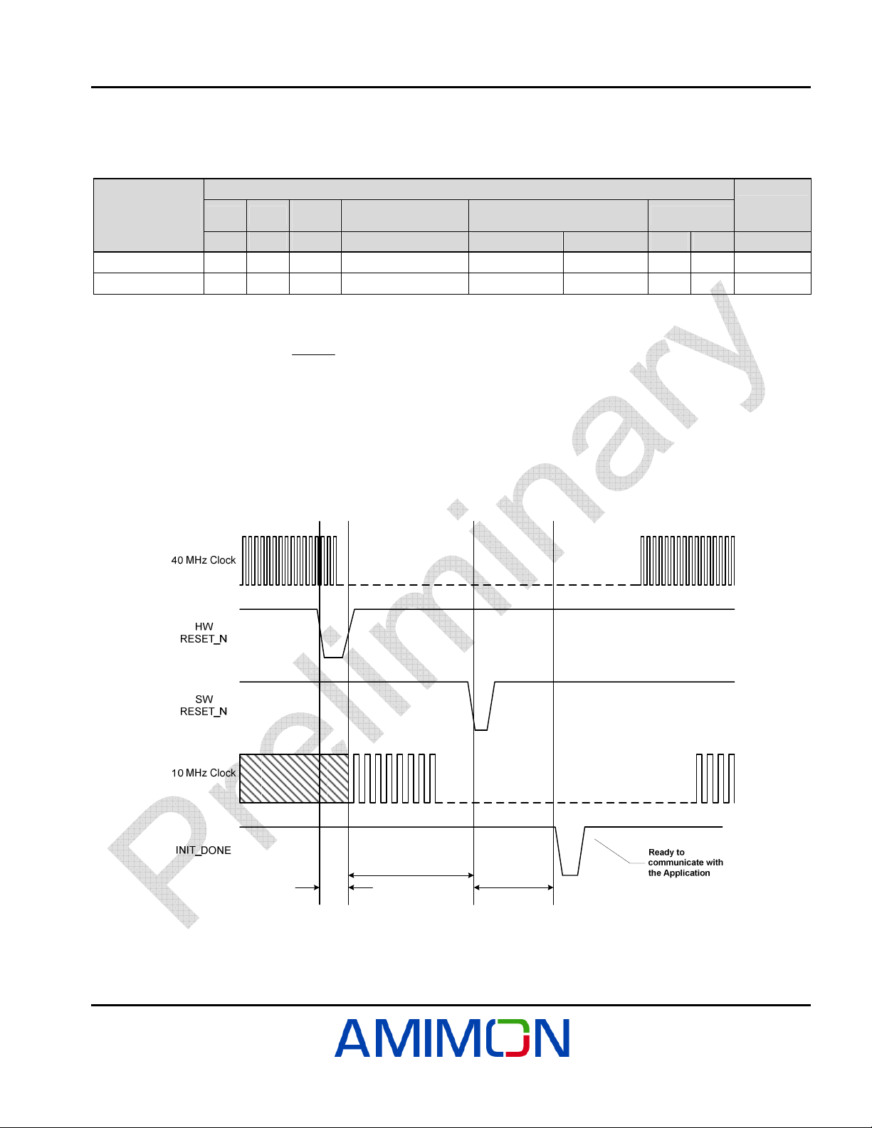
The AMN11100 has one hard
RESET
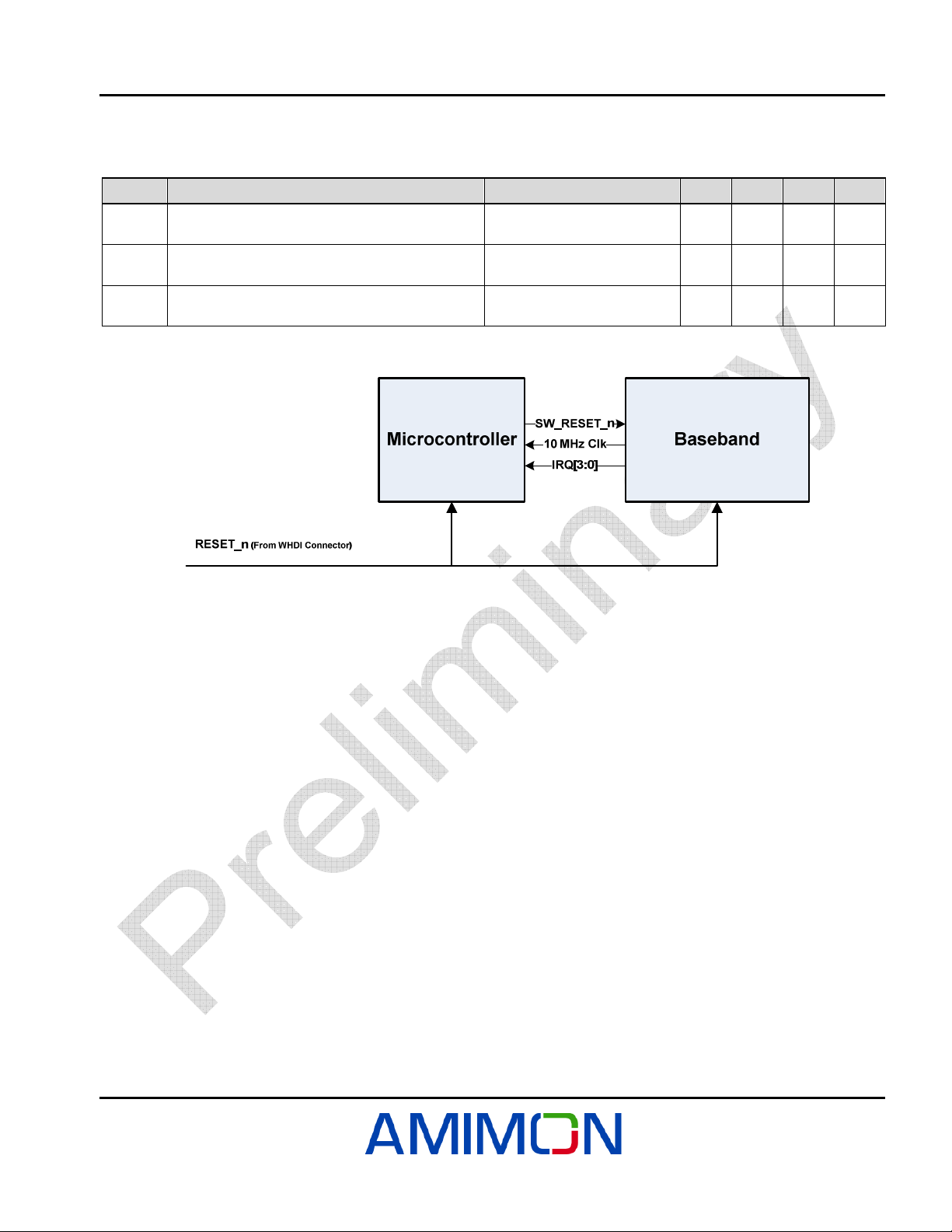
input pin connected directly to the AMN2110 and to the STM32F uC, as
described in 3.4. Assertion of the STM32F reset switches the clock of uC to the internal oscillator until the
Albatross does not assert an INIT_DONE interrupt. Assertion of the Albatross reset enables the generation of the
10 MHz clock. After a hard reset, the MAC asserts the SW reset signal which just clears the registers without
resetting the clock generation scheme.
When the INIT_DONE is asserted, it indicates the completion of the Albatross initialization and that the 10 MHz
clock is stable. At that point, the uC switches to the external clock source from the Albatross and enable
communication with the application microcontroller.
ST
T
rst
clkrstT−
T
init
Figure 10: Reset Time Diagram
Version 0.4
AMIMON Confidential 14
Page 21
The following table specifies the timing parameters -
Table 7: Reset Timing Requirements
Interfaces
Symbol
T
RST-CLK
T
ST,RST
Time from assertion of the HW reset until valid
clock is generated
Time from assertion of the HW reset until the
Parameter Condition MIN TYP MAX Units
40 MHz clock is valid – few
us after power up
Power is stable 4.5 ms
STM32F completes the internal initialization
T
INIT
Time from assertion of the HW/SW reset until the
1.7 ms
AMN2110 completes the internal initialization
The following figure specifies the reset schema and related signals -
Figure 11: Reset Mechanism
300 ns
Version 0.4
AMIMON Confidential 15
Page 22

Interfaces
Version 0.4
AMIMON Confidential 16
Page 23
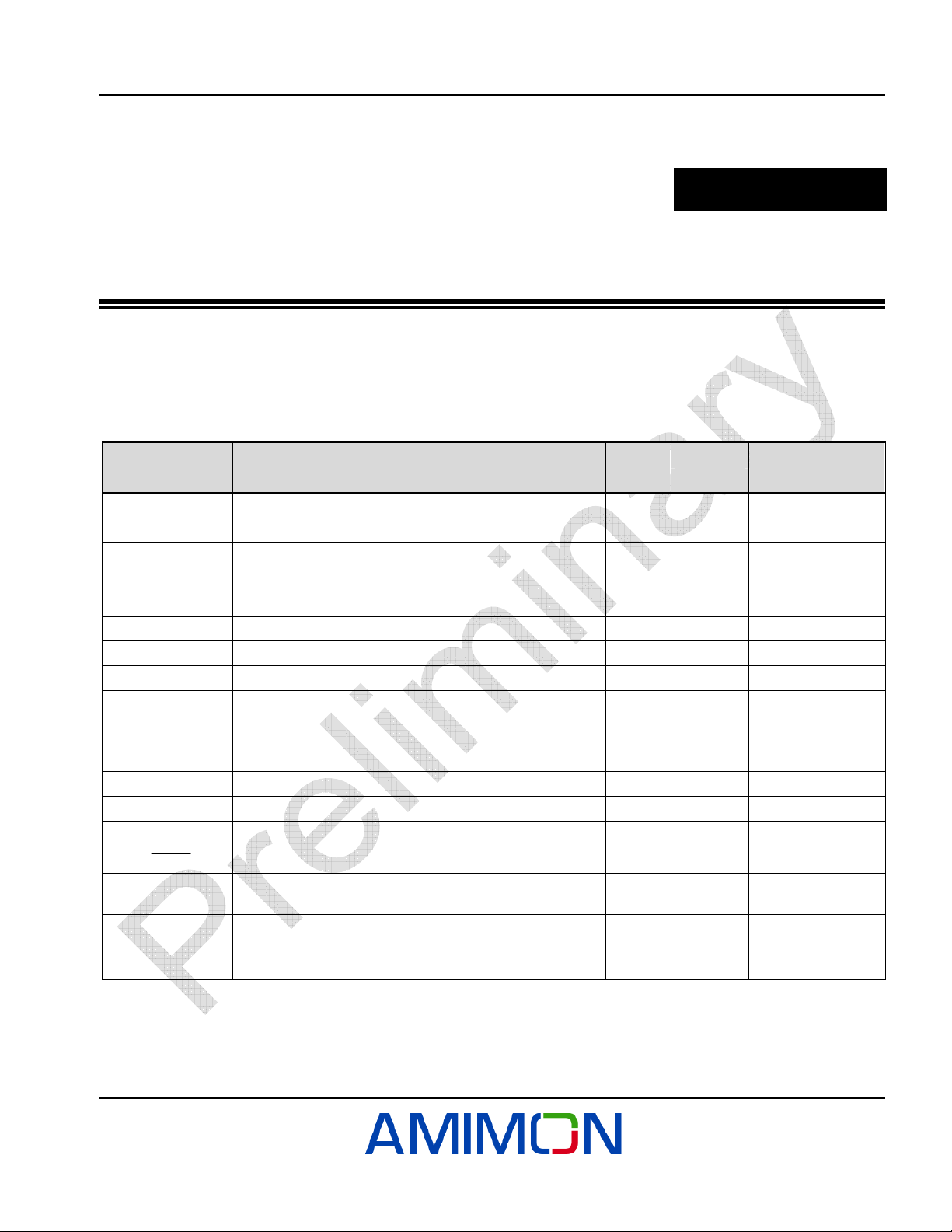
4.1 Signals
Table 8: WHDI Connector Signals
WHDI Connector Pins
Chapter 4
WHDI Connector Pins
# of
Pins
30 D[29:0] 30-bit RGB (10:10:10) or YCrCb (10:10:10) Video In
1 DCLK Video data clock Video In Up to 78.125 MHz
1 DE Data enable Video In
1 H_SYNC Horizontal sync Video In
1 V_SYNC Vertical sync Video In
1 SPDIF SPDIF audio interface Audio In
1 SD I2S audio interface Serial Data signals Audio In
1 SCLK I2S continuous serial clock Audio In Up to 3.072Mbps
1 WS(LRCLK)
1 MCLK
1 SDA Two-wire Serial Bus Data (Slave Mode) Control I/O Control I/F for WHDI
1 SCL Two-wire Serial Bus Clock (Slave Mode) Control In Control I/F for WHDI
1 INT Interrupt from WHDI module Control Out
1
2 TBD[5:4]
14 3.3V VCC Power Power
17 GND Ground Power Power
Pin Name Description/Functionality Group
Audio In
Audio NA
TBD TBD
RESET
I2S Word Select (Left/right clock) which defines also the
sampling rate
I2S master clock coherent to WS according to specified
ratio
Reset / Power-down line Control In
TBD4, TBD5 are reserved in AMN11310, as an option for
RS232 connection to STM32F UART2.
Direction
Tx
Remarks
Rate is adjustable
on RX side
300 mA maximum
rating per pin
†
Data in this table is preliminary.
Version 0.4
AMIMON Confidential 17
Page 24
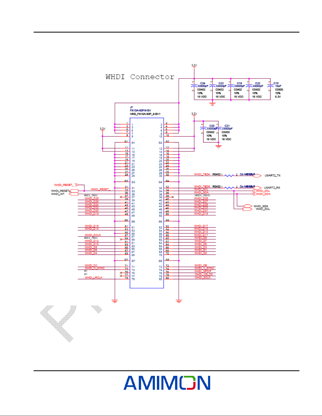
4.2 Connector Schematics
WHDI Connector Pins
Figure 12: WHDI Connector
Version 0.4
AMIMON Confidential 18
Page 25
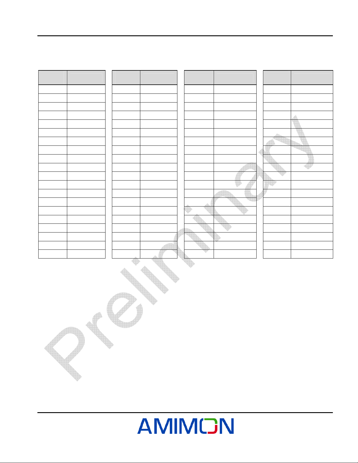
4.3 Pin List
Table 9: Tx WHDI Connector Pin List
WHDI Connector Pins
Pin
Number
1
3
5
7
9
11
13
15
17
19
21
23
25
27
29
31
33
35
37
39
Signal
3.3V
3.3V
3.3V
3.3V
3.3V
3.3V
3.3V
GND
GND
GND
GND
GND
GND
GND
GND
GND
WHD_RESET_
WHDI_INT
NC
WHDI_D28
Pin
Number
2
4
6
8
10
12
14
16
18
20
22
24
26
28
30
32
34
36
38
40
Signal
3.3V
3.3V
3.3V
3.3V
3.3V
3.3V
3.3V
GND
GND
GND
GND
GND
GND
GND
WHDI_TBD4
WHDI_TBD5
WHDI_SCL
WHDI_SDA
NC
WHDI_D29
Pin
Number
41
43
45
47
49
51
53
55
57
59
61
63
65
67
69
71
73
75
77
79
Signal
WHDI_D26
WHDI_D24
WHDI_D22
WHDI_D20
WHDI_D18
WHDI_D16
WHDI_D14
GND
WHDI_DCLK
NC
WHDI_D12
WHDI_D10
WHDI_D8
WHDI_D6
WHDI_D4
WHDI_D2
WHDI_H_SYNC
NC
NC
WHDI_LRCLK
Pin
Number
42
44
46
48
50
52
54
56
58
60
62
64
66
68
70
72
74
76
78
80
Signal
WHDI_D27
WHDI_D25
WHDI_D23
WHDI_D21
WHDI_D19
WHDI_D17
WHDI_D15
WHDI_D13
WHDI_D11
WHDI_D9
WHDI_D7
WHDI_D5
WHDI_D3
WHDI_D1
WHDI_D0
WHDI_DE
WHDI_V_SYNC
WHDI_SPDIF
WHDI_I2S_D0
WHDI_SCLK
Version 0.4
AMIMON Confidential 19
Page 26

WHDI Connector Pins
Version 0.4
AMIMON Confidential 20
Page 27
Electrical Specifications
Chapter 5
Electrical Specifications
5.1 Operating Conditions and Electrical Characteristics
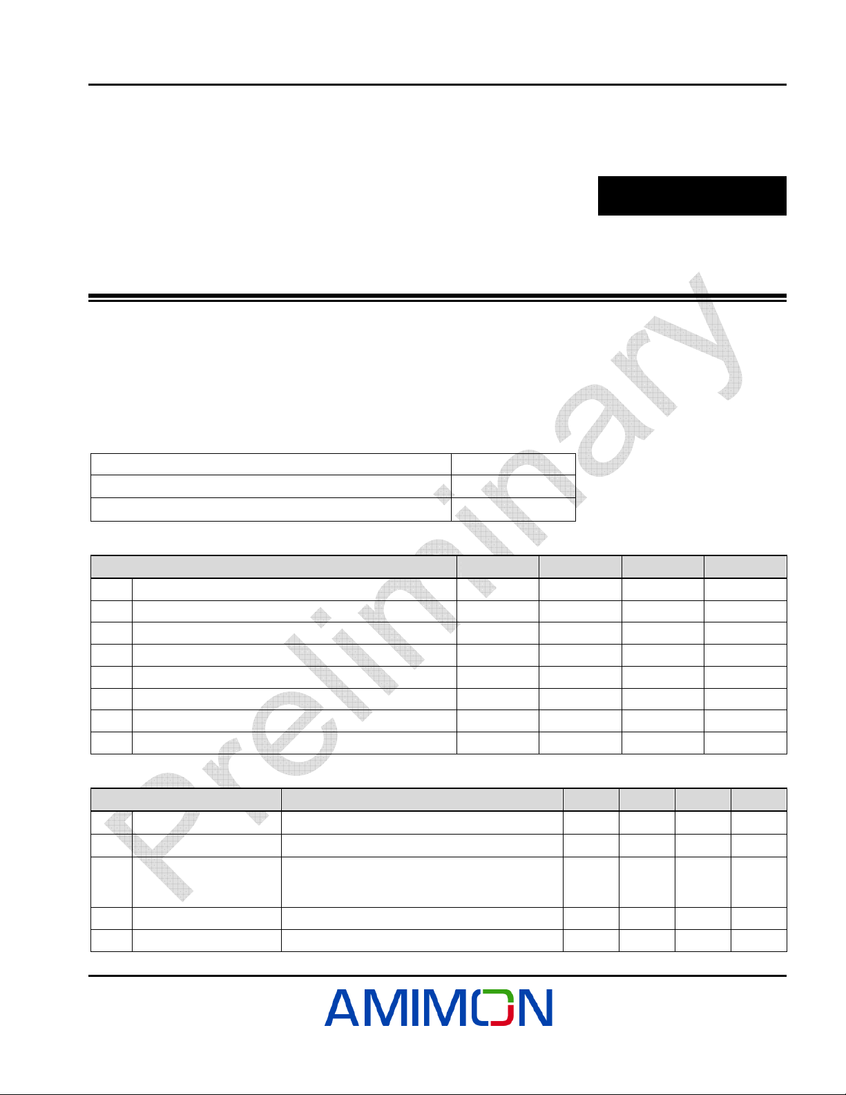
The following tables describe the operating conditions and electrical characteristics required for working with the
AMN11310.
Table 10: Absolute Maximum Ratings over Operating Case Temperature Range
Supply input-voltage range, VI 0 to 3.6 V
Ambient temperature range
Storage temperature range, Tstg
0°C to 70°C
-40°C to 125°C
Table 11: Recommended Operating Conditions
Parameter Min. Typ. Max. Unit
DVDD Module supply voltage 3.15 3.3 3.45 V
VSS Supply ground 0 V
VIH High-level input voltage 0.7 DVDD V
VIL Low-level input voltage 0.3 DVDD V
VOH High-level output voltage (DV
VOL Low-level output voltage (DV
IOH High-level output current -8 mA
IOL Low-level output current 8 mA
= MIN, I
DD
= MIN, I
DD
= MAX) 0.8 DVDD V
OH
= MAX) 0.22 DVDD V
OL
Table 12: Electrical Characteristics over Recommended Range of Supply Voltage and Operating Conditions
Parameter Test Conditions Min. Typ. Max. Unit
I
Input current VI = VSS to DVDD
I
I
Off-state output current VO = DV
OZ
I
Module supply
DVDD
C
Input capacitance 10 pF
i
C
Output capacitance 10 pF
o
DV
DD
with activity on all I/O terminals and transmitting
in maximum power.
or 0 V
DD
= Max., Video Clock = 74.25 MHz,
1800 mA
±
±
20
20
µ
A
µ
A
Version 0.4
AMIMON Confidential 21
Page 28

5.2 RF Characteristics (TBD)
Electrical Specifications
Version 0.4
AMIMON Confidential 22
Page 29
Design Guidelines
Chapter 6
Design Guidelines
6.1 Digital Layout Recommendation
To better understand the layout guidelines, please refer to the AMN11310 schematics which are part of the HDK
package.
6.1.1 Stack up
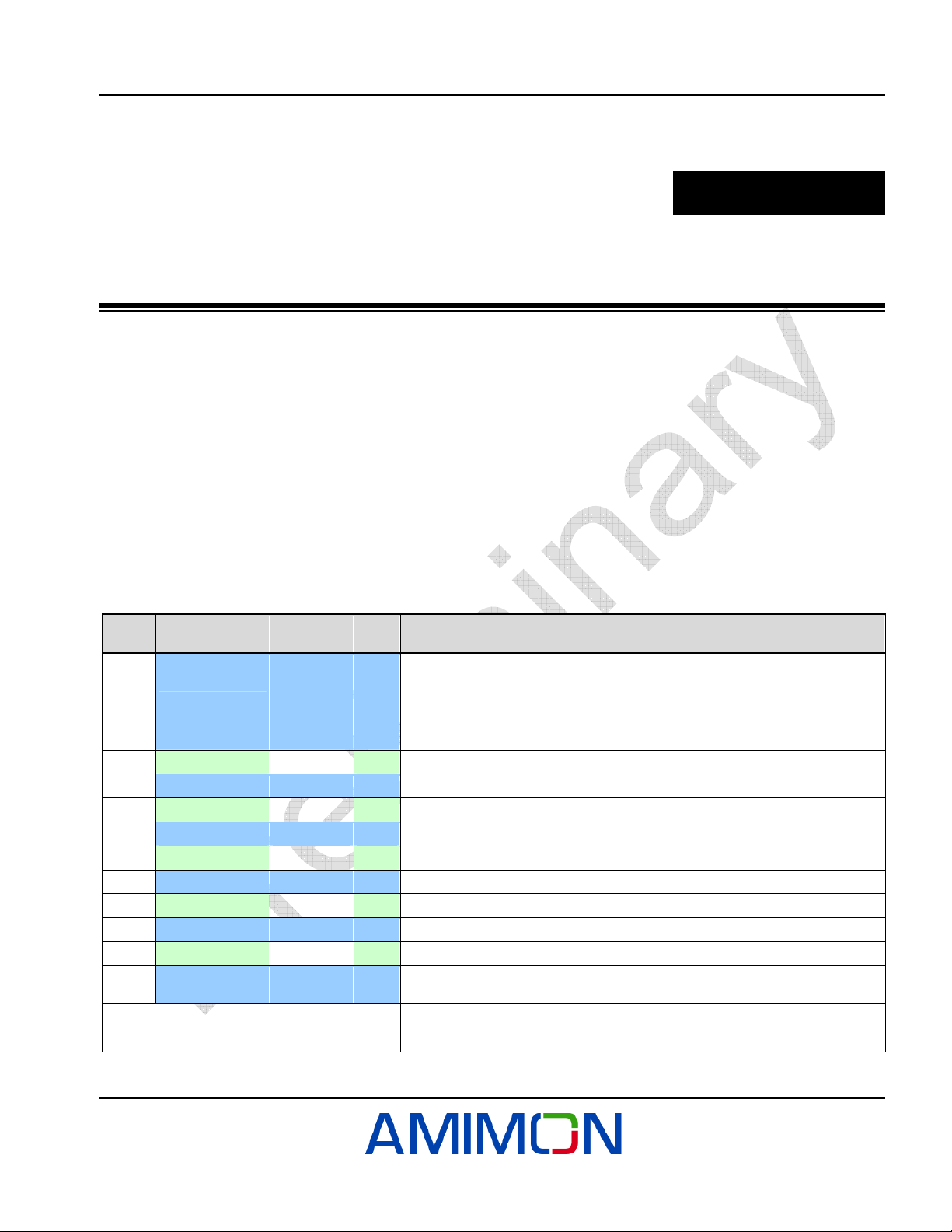
Recommended stack up for six layers design:
• Total thickness: 1.15mm
• Tolerance thickness: 10%
Table 13: Digital Layout Recommendation
Lay.
No.
1 Component side
Space 8.6 mil
2 Ground 2 oz
Space 4 mil
3 Ground 2 oz
Space 4 mil
4 Power / Ground 2 oz
Space 4 mil
5 Ground 2 oz
Space 8.6 mil
6 Print Side (PS) 1-1.5 oz Trace Width - 5. mil, Separation between differential lines – 6 mil, differential
Board Thickness 1.15 MM +\- 10%
Material FR4 HITG
Layer Name
(CS)
Layer Stack-
up
1-1.5 oz 1) Trace Width -14mil, Separation -12 mil (to ground plane) - 50 OHM COPLANAR
Control Impedance/Note's
2) Trace Width - 5.5 mil, Separation between differential lines – 5.5 mil, differential
impedance - 103 OHM.
3) Trace Width – 5 mil, Separation between differential lines – 6 mil, differential
impedance - 107 OHM.
impedance - 107 OHM.
Version 0.4
AMIMON Confidential 23
Page 30

Design Guidelines
6.1.2 General Guidelines
• Keep traces as short as possible.
• Traces should be routed over full solid reference plans.
• Sensitive lines like reset and clocks should be routed with special care.
These lines should be routed over full solid power plans (ground or power).
Traces should be routed at least 2 times the trace width away from other lines in the same routing layer.
Place a series resistor ~30 ohm at the clock source.
• Keep digital signals away from the analog side.
6.1.3 WHDI Lines
• Place series resistors on all output lines (near the outputs pins).
• Series resistors on input lines are unnecessary. (The series resistors should be placed on the interface
board.)
6.1.4 Power and Ground
• Use a solid ground plan.
• Ground plans separation is unnecessary.
• Place decoupling capacitors near power pins. (Refer to the schematics and BOM for recommended values.)
• Analog power pins should be filtered with ferrite beads. (Refer to the schematics and BOM for recommended
values.)
• Add as many ground vias as possible, for better ground connections between layers and better heat
dissipation.
6.2 RF Design Recommendation
6.2.1 RF Components
All passive components must have compatible performance with components used in the Amimon reference
design.
6.2.2 Power Management
The RF power rail 3.3V_RAIL is separated from the digital power rail 3.3 with ferrite bead.
Version 0.4
AMIMON Confidential 24
Page 31
6.3 Test Points and Jumpers
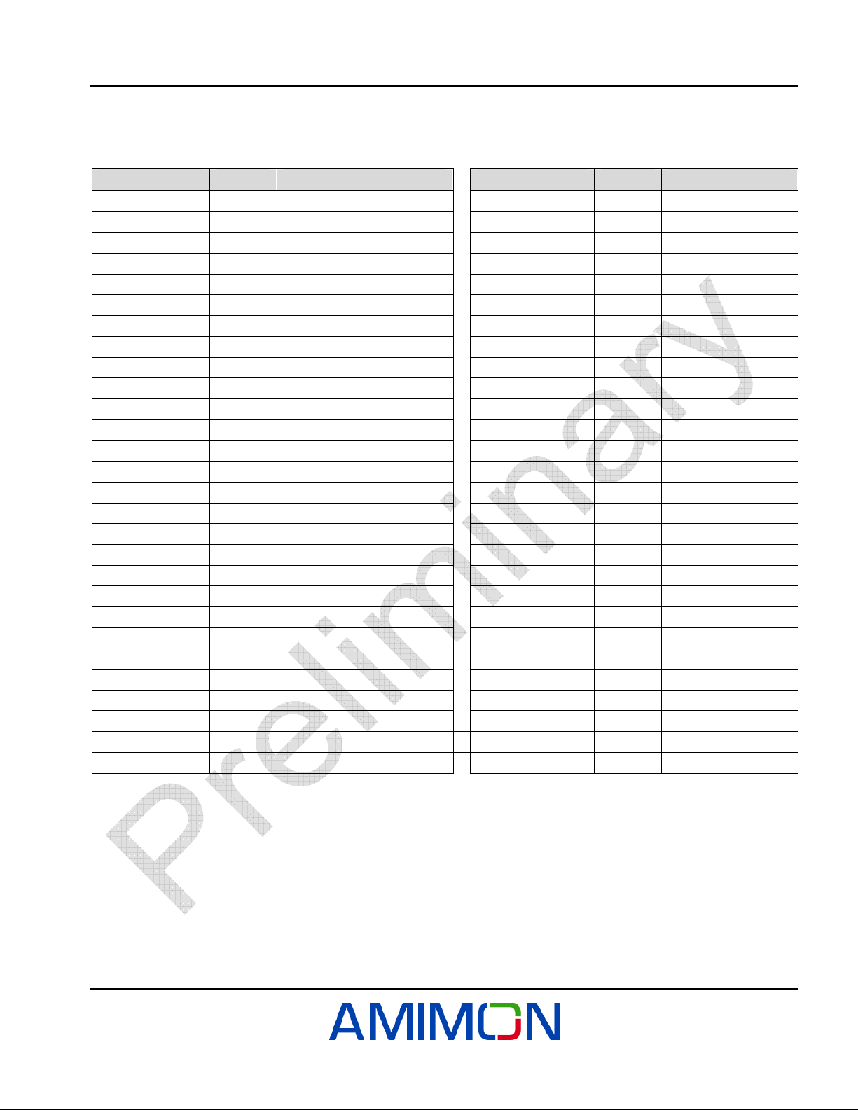
Table 14 test points and jumpers
Design Guidelines
Reference Name Type Functionality Reference Name Type Functionality
TP1 SMD RSSI_DETECT TP29 SMD 3.3V
TP2 SMD RFSPI_ODUT TP30 SMD 3.3V
TP3 SMD RFSPI_CS TP31 SMD 3.3V
TP4 SMD RFSPI_CLK TP32 SMD GND
TP5 SMD LD_0 TP33 SMD GND
TP6 SMD GND TP34 SMD ALBATROSS_TDO
TP7 TH GND TP35 SMD GND
TP8 SMD GND TP36 SMD HW_ID_1
TP9 TH 1.2V TP37 SMD 3.3V
TP10 TH GND TP38 SMD HW_ID_0
TP11 SMD CLK40M TP39 TH 3.3V
TP12 SMD TX_SHDW N_B_0 J1 SMD RF- UFL CON
TP13 SMD RSSI_S_0 J2 SMD RF- UFL CON
TP14 TH GND J3 SMD RF- UFL CON
TP15 SMD GND J4 SMD RF- UFL CON
TP16 SMD 3.3V J5 SMD RF- UFL CON
TP17 SMD 3.3V J6 SMD RF- UFL CON
TP18 SMD GND J7 SMD WHDI CON
TP19 TH GND J8 SMD UC JTAG
TP20 SMD UC_MAC_CLK JP1 pin 1-2 JUMPER MAC_TXD
TP21 SMD 3.3V JP1 pin 2-3 JUMPER ALB_TXD
TP22 SMD GND JP2 pin 1-2 JUMPER MAC_RXD
TP23 SMD MAC_TDI JP2 pin 2-3 JUMPER ALB_RXD
TP24 SMD MAC_TCK JP3 JUMPER BOOT0
TP25 SMD 3.3V SW1 SWITCH RF_TEST_SW
TP26 SMD MAC_RST
TP27 SMD MAC_TRST SW3 SWITCH RF_TEST_SW
TP28 SMD MAC_TMS SW4 SWITCH RF_TEST_SW
SW2 SWITCH RF_TEST_SW
Version 0.4
AMIMON Confidential 25
Page 32

Design Guidelines
Version 0.4
AMIMON Confidential 26
Page 33
Mechanical Dimensions
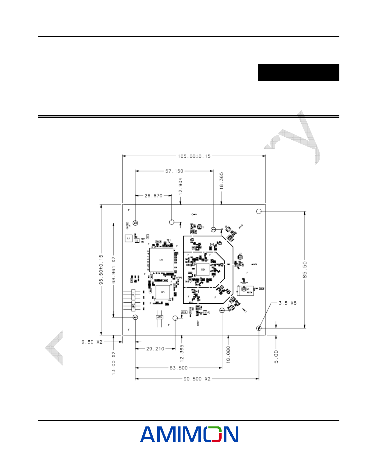
The following shows the mechanical dimensions for the AMN11310:
Mechanical Dimensions
Chapter 7
Figure 13: Mechanical Dimensions Top View
Version 0.4
AMIMON Confidential 27
Page 34
Mechanical Dimensions
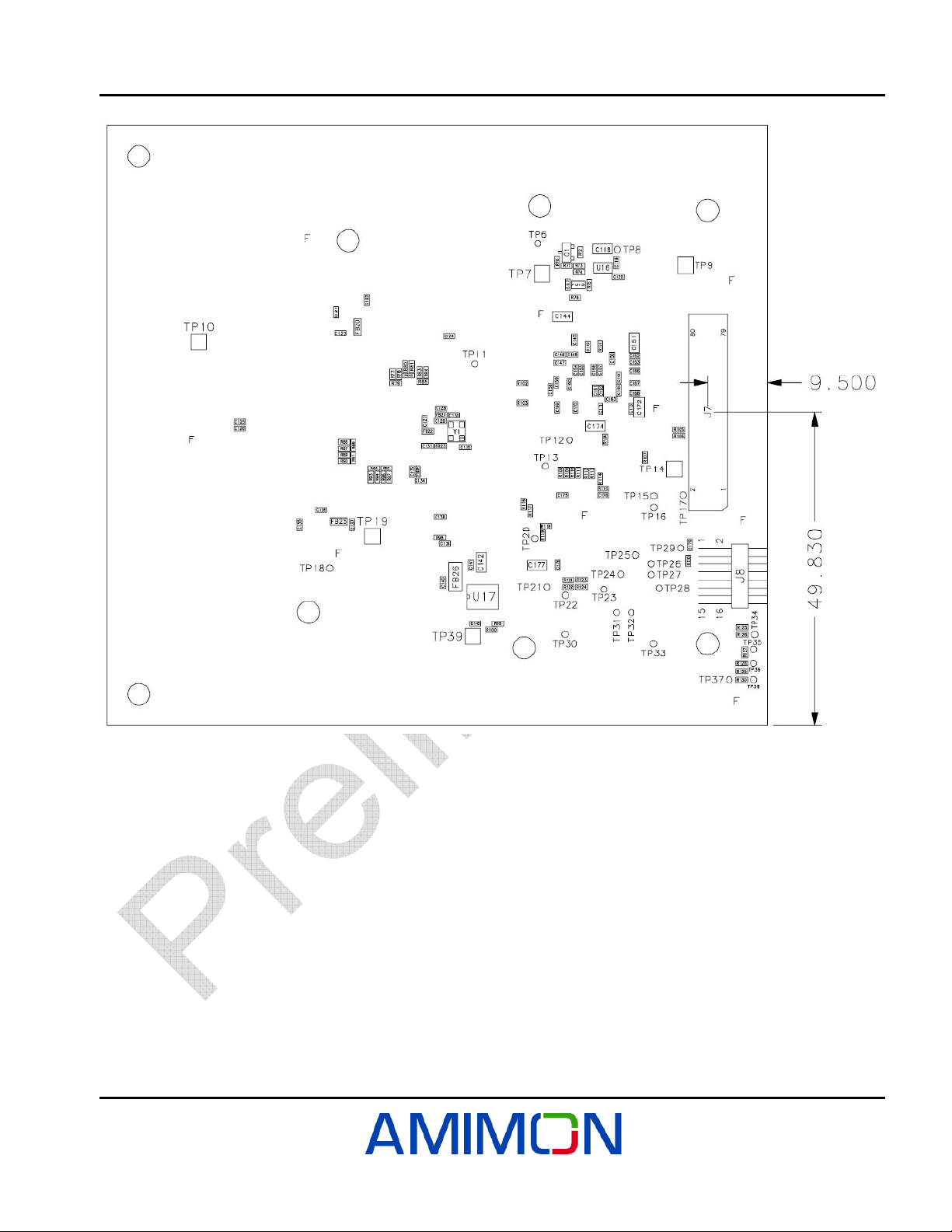
Figure 14: Mechanical Dimensions Bottom View
Version 0.4
AMIMON Confidential 28
Page 35
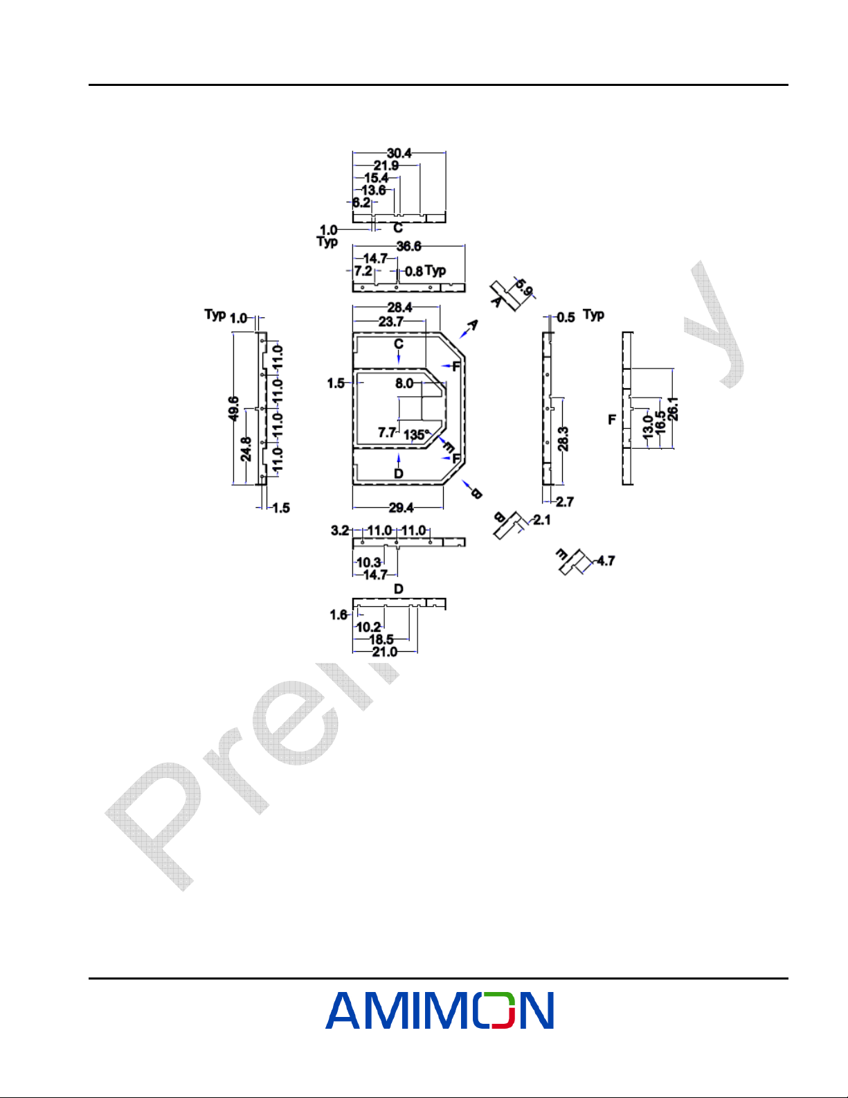
7.1 RF Shield Frame and Cover
Mechanical Dimensions
Figure 15: RF-Shield Frame
Version 0.4
AMIMON Confidential 29
Page 36
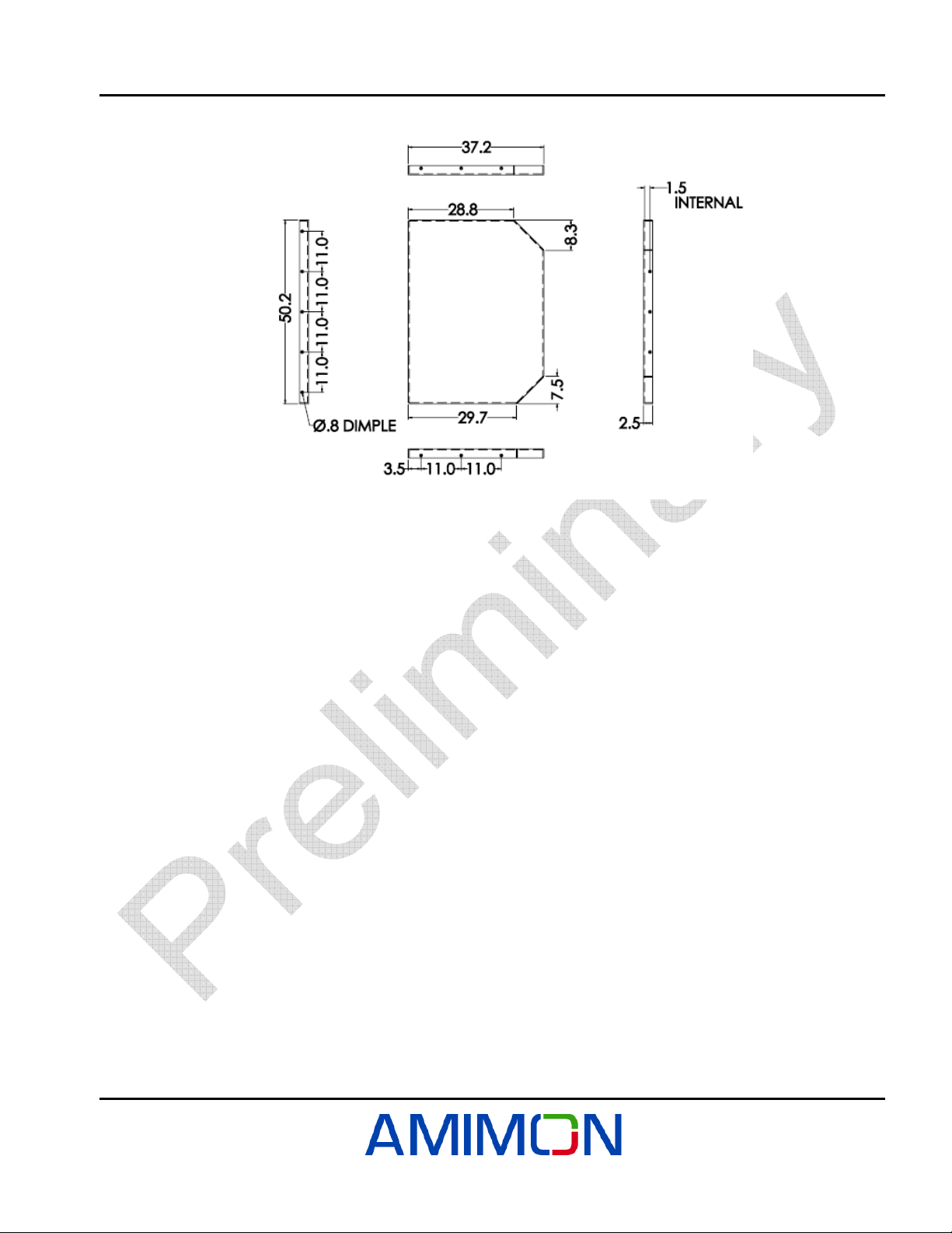
Figure 16: RF-Shield Cover
Mechanical Dimensions
Version 0.4
AMIMON Confidential 30
 Loading...