


American Megatrends, Inc.
Series 87 Enterprise-IV
80486 EISA VLB
Motherboard
User's Guide
MAN-687
9/8/94

© Copyright 1985-2010 American Megatrends, Inc.
All rights reserved.
American Megatrends, Inc.
5555 Oakbrook Parkway, Building 200,
Norcross, GA 30093
This publication contains proprietary information which is protected by copyright. No part of this publication may be reproduced, transcribed,
stored in a retrieval system, translated into any language or computer language, or transmitted in any form whatsoever without the prior written
consent of the publisher, American Megatrends, Inc.
Limited Warranty
Buyer agrees if this product proves to be defective, that American Megatrends, Inc. is only obligated to replace or refund the purchase price of
this product at American Megatrend's discretion according to the terms and conditions of the warranty card accompanying the Enterprise-IV
motherboard. American Megatrends shall not be liable in tort or contract for any loss or damage, direct, incidental or consequential. Please see
the Warranty Registration Card shipped with this product for full warranty details.
Limitations of Liability
In no event shall American Megatrends be held liable for any loss, expenses, or damages of any kind whatsoever, whether direct, indirect,
incidental, or consequential, arising from the design or use of this product or the support materials provided with the product.
Trademarks
American Megatrends acknowledges the following trademarks:
Intel is a registered trademark of Intel Corporation.
MS-DOS, Xenix, and Microsoft are registered trademarks of Microsoft Corporation. Microsoft Windows and Windows NT are trademarks of Microsoft Corporation.
IBM, AT, PS/2, VGA, OS/2, and EGA are registered trademarks of International Business Machines Corporation. XT and CGA are trademark s of I n ter national Busines s Mach ines Corporation.
Fujitsu is a registered trademark of Fujitsu America, Inc.
Motorola is a registered trademark of Motorola Corporation.
Oki is a registered trademark of Oki America, Inc.
NEC is a registered trademark of NEC Corporation.
Samsung is a registered trademark of Samsung Electronics Corporation.
Siemens is a trademark of Siemens Corporation.
Mitsubishi is a registered trademark of Mitsubishi Electronics of America.
Unix is a registered trademark of American Telephone and Telegraph Company Bell Laboratories.
Weitek is a trademark of Weitek, Inc.
Toshiba is a registered trademark of Kabushiki Kaisha Toshiba.
Revision History
6/8/93 Initial release.
10/6/93 Add new AMIBIOS Setup options.
9/8/94 Added information from errata sheets.

Table of Contents
Chapter 1 Introduction to VL-Bus
Chapter 2 Enterprise-IV Description
Chapter 3 Installation
Chapter 4 AMIBIOS Power-On Self Test
Chapter 5 AMIBIOS Setup
Section 1 Running AMIBIOS Setup
Section 2 STANDARD CMOS SETUP
Section 3 ADVANCED CMOS SETUP
..........................................................................................................................................................................................
Step 1 Un pack th e Motherboard
Step 2 Set Switch and Jumper Options
Step 3 Install Memory
Step 4 Insta ll U pgrade Processor
Step 5 Install the Motherboard
Step 6 Connect the Power Supply
Step 7 Connect the Keyboard
Step 8 Connect the Mouse
Step 9 Connect Cables
Step 10 Install Adapter Cards
Step 11 Perform Initial Test and Configuration
Date And Day Configuration
Time Configuration
Hard Disk Drive C: and D:
Using Auto Detect Hard Disk
Hard Disk Drive Types
Floppy Drive A and Floppy Drive B:
Primary Display
Keyboard
Typematic Rate Programming
Typematic Rate Delay
Typematic Rate
Mouse Support Option
Above 1 MB Memory Test
Memory Test Tick Sound
Memory Parity Error Checking
System Boot Up Num Lock
Floppy Drive Seek At Boot
System Boot Up Sequence
System Boot UP CP U Speed
External Cache Memory
Internal Cache Memory
Password Checking Option
Video ROM Shadow C000,32K
Adaptor ROM Shadow C800,32K
Adaptor ROM Shadow D000,64K
......................................................................................................................................................................
..................................................................................................................................................................
.................................................................................................................................................................................
..................................................................................................................................................................
.............................................................................................................................................................................
...................................................................................................................................................................
.........................................................................................................................................
...............................................................................................................................
.........................................................................................................................................................
........................................................................................................................................
............................................................................................................................................
.......................................................................................................................................
..............................................................................................................................................
..................................................................................................................................................
........................................................................................................................................................
.............................................................................................................................................
..................................................................................................................
..........................................................................................................................................................
.....................................................................................................................................................
...............................................................................................................................................
..............................................................................................................................................
............................................................................................................................................................
.................................................................................................................................................
.............................................................................................................................................
.......................................................................................................................................................
..................................................................................................................................
...............................................................................................................................................
............................................................................................................................................
.........................................................................................................................................................
........................................................................................................................................................
.................................................................................................................................................
..................................................................................................................................................
...........................................................................................................................................
................................................................................................................................................
................................................................................................................................................
.................................................................................................................................................
...............................................................................................................................................
.....................................................................................................................................................
......................................................................................................................................................
.................................................................................................................................................
.........................................................................................................................................
......................................................................................................................................
......................................................................................................................................
1
3
11
11
13
16
19
22
24
27
27
28
31
38
39
47
49
53
53
53
54
54
55
56
56
56
57
58
58
58
58
58
59
59
59
59
59
60
60
60
60
61
61
61
Enterprise-IV EISA VLB Motherboard User's Guide

Table of Contents,
Continued
Chapter 5 AMIBIOS Setup, cont'd
Section 4 ADVANCED CHIPSET SETUP
Section 5 AMIBIOS Password Support
Section 6 Hard Disk Utility
Appendix A Temperature and Power Considerations
Appendix B Heat Dissipati on
Appendix C EISA Configuration Worksheets
Appendix D Flash EPROM Support
Index
.....................................................................................................................................................................................................................
Adaptor ROM Shadow E000,64K
System ROM Shadow F000,64K
Shadow RAM Write Protec tion
Boot Sector Virus Protection
LBD Sampling Point
Cache Write Back
Non-Cacheable Area 1
Non-Cacheable Area 1 Size
Non-Cacheable Area 1 Start
I/O Recovery Select
Hidden Refresh
On Board Serial Port 1
On Board Serial Port 2
On Board Parallel Port
On Board Floppy Controller
On Board IDE Controller
..............................................................................................................................................................................
...........................................................................................................................................................
...............................................................................................................................................................
........................................................................................................................................................
............................................................................................................................................................
...................................................................................................................................................................
........................................................................................................................................................
........................................................................................................................................................
........................................................................................................................................................
..................................................................................................................................................................
................................................................................................................................................................
......................................................................................................................................
........................................................................................................................................
..........................................................................................................................................
..............................................................................................................................................
................................................................................................................................................
...............................................................................................................................................
..........................................................................................................................................
...............................................................................................................................................
....................................................................................................................................................
................................................................................................................................................
......................................................................................................................................
...................................................................................................................................................
61
62
62
63
63
63
64
64
64
65
65
67
67
68
68
68
68
69
71
79
81
83
101
109
Preface

Preface
To the OEM, VAR, or System Integrator
Thank you for pur chasing the high performance Series 87 Ent erprise-IV EISA VL-Bus motherboard from
American Megatrends. It is assumed that you have also licensed the rights to use the technical documentation for the
Enterprise-IV. This manual was written for American Megatrends customers who are system integrators, VARs, or
OEMs to assist in the proper installation and operation of the Enterprise-IV motherboard. This manual is not meant
to be read by the computer owner who purchases a computer with the Enterprise-IV motherboard. It is assumed that
you, the computer manufacturer, will use this manual as a sourcebook of information, and that parts of this manual
will be included in the computer owner's manual.
Technical Support
If an Enterprise-IV motherboard fails to operate as described or you are in doubt about a configuration option, please
call technical support at 404-246-8600.
Acknowledgments
This manual was written by Vivek Saxena, Paul Narushoff, and Robert Cheng.
Enterprise-IV EISA VLB Motherboard User's Guide

American Megatrends BBS
The American Megatrends BBS permits OEMs, VARs, and system integrators to access technical information about
American Megatrends motherboard, peripheral card, and BIOS products. Product Engineering Change Notices, Tech
Tips, Technical Notes, and complete technical manuals are available on the BBS.
Data Transmission Rates
The BBS automatically handles modems with data transmission rates from 1,200 to 14,400 bps. If using an HST
modem, call 404-246-8780. If using a non-HST modem, call 404-246-8782.
BBS Phone Numbers
The following table lists the characteristics of the BBS phone numbers. The BBS requires no parity, 8 data bits, and
1 stop bit.
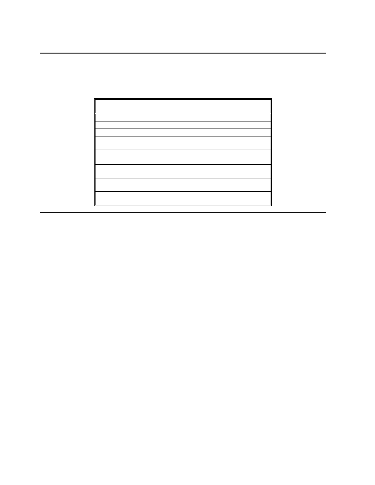
Phone Number Characteristics
404-246-8780 Supports HST and v.42bis.
404-246-8781 Supports HST and v.42bis.
404-246-8782 Dual standard. Can handle 2400 or 9600 bps. Supports v.32bis
404-246-8783 Supports v.32bis and v.42bis.
and v.42bis. Can handle up to 14,400 baud.
Packing Slip
You should have received:
• an Enterprise-IV EISA VLB motherboard,
•the
Enterprise-IV Motherboard User's Guide,
• a diskette containing the American Megatrends ECU and EISA configuration files, and
•the
American Megatrends ECU User's Guide.
Preface

Chapter 1
Introduction to VL-Bus
The Series 87 Enterprise-IV EISA Local Bus Motherboard conforms to the VESA® (Video Electronics
Standards Association) VL-Bus® specifications as well as the EISA (Extended Industry Standard
Architecture) specification.
The VL-Bus
The VL-Bus is designed to standardize the hardware interface of peripherals connected to a
microprocessor-level local bus. The VL-Bus Specification is a standard set of interface, architecture,
timings, electrical, and physical specifications that permits all VL-Bus products to be totally
interchangeable.
VL-Bus is Based on 80486 Local Bus Design
The general architecture of the VL-Bus is designed to Intel® 80486 CPU local bus standards with
additional hardware functions that accommodate VL-Bus master devices and facilitate the system I/O bus
interface. The timing specifications allow VL-Bus devices to operate at the full 32-bit 80486 CPU
bandwidth.
seven EISA expansion slots ar e EISA (NOT Vl-Bus) bus mastering slots.
Both VL-Bus slots on the Enterprise-IV motherboard have bus mastering capability.
Six of the
EISA and Local Bus Expansion
The American Megatrends Enterprise-IV EISA Local Bus motherboard has seven expansion slots. Six of
these slots are EISA bus mastering slo t s. One is an EISA non-bus master slot. Two slot s are VL-Bus bus
mastering slots. The VL-Bus slots consist of a standard EISA 32-bit slot connector and an inline VL-Bus
connector.
Enterprise-IV EISA VLB Motherboard User's Guide

Introduction to VL-Bus,
Continued
The following graphic shows the EISA and VL-Bus expansion slots. You can install 16-bit ISA or 32-bit
EISA adapter cards in any expansion slot, including the VL-Bus slots. The VL-Bus expansion slots include
one EISA slot that has both EISA and VL-Bus bus mastering (SLOT 6) slot and one VL-Bus master slot
(SLOT 7) that is an EISA non-bus mastering slot.
EISA or ISA adapter cards have no VL-Bus functionality when installed in a VL-Bus expansion slot.
The current VL-Bus expansion socket specification includes a 16-bit MCA® (Micro Channel Architecture)
expansion socket inline with a standard 32-bit EISA expansion socket connector.
A future VL-bus specification will use a 32-bit MCA connector (a total of 64 bits). The VL-Bus
specification supports 32-bit EISA adapter cards.
The VL-Bus Adapter Cards have a different set of connectors on the bottom of the card and will only fit in
the VL-Bus expansion sl ots.
Chapter 1 Introduction to VL-Bus

Chapter 2
Enterprise-IV Description
Dimensions
The American Megatrends 80486 Enterprise-IV EISA Local Bus motherboard is approximately 8½" by
13", similar in size to a standard Baby AT® motherboard. The mounting hole locations permit the
motherboard to be used with any Baby AT chassis. The height of the components is no more than 1½
inches, but allow 2 inches of clearance for the power supply connectors, as shown below.
Enterprise-IV EISA VLB Motherboard User's Guide
Specifications
Processor Type and Speed
Microprocessors can be installed in two sockets: the CPU socket and the Upgrade Socket. The motherboard
supports the following processors:
Processor in ZIF Socket
(Upgrade Socket)
Empty 486SX 20, 25, or 33 MHz
Empty 486DX 20, 25, or 33 MHz
486DX empty 25, 33, or 50 MHz
486DX2 empty 25 MHz (50 MHz internal),
486SX 486SX 20 or 25 MHz
P24 empty 25 MHz or 33 MHz
P24T empty 25 MHz (50 MHz internal),
487SX 486SX
Intel Overdrive® (P23T) empty 25 MHz (50 MHz internal),
PQFP Processor Frequency
33 MHz (66 MHz internal)
33 MHz (66 MHz internal)
20, 25, or 33 MHz
(or none)
33 MHz (66 MHz internal)
CPU Sockets
The Enterprise-IV may come with a factory-mounted 486DX or 486SX. It also has a 240-pin PGA ZIF
upgrade processor socket for an Intel 80486DX, 80486SX, 80486DX2, or upgrade processor CPU.
If both the PQFP and ZIF sockets contain CPUs, the CPU in the ZIF socket will be the active CPU.
The Enterprise-IV motherboard also will support future Intel processors.
Chapter 2 Description

Specifications,
Programmable Crystal Oscillator
The Enterprise-IV motherboard has a programmable crystal oscillator that supports all possible
motherboard frequencies.
Heat Sink for 50 and 66 MHz CPUs
The Enterprise-IV EISA Local Bus motherboard has a heat sink for all motherboards equipped with a 50
MHz 80486DX or 25 MHz (operates at 50 MHz internally) or 33 MHz (operates at 66 MHz internally)
80486DX2 to help dissipate heat. See page 91 for additional information about heat dissipation.
Processor Speeds
The Enterprise-IV operates at either of two speeds: high or low. High speed is set at time of manufacture to
the processor speed (25, 33, 50, or 66 MHz). A low speed that is approximately the same speed as an
original IBM® AT is simulated by adding extra cycles. The clock speeds can be changed via the <Ctrl>
<Alt> <+> and <Ctrl> <Alt> <-> keychords. These keychords can be changed by the OEM via AMIBCP.
System Memory
The Enterprise-IV EISA VLB motherboard supports up to 256 MB of onboard memory via four banks of
256 KB x 36, 1 MB x 36, 4 MB x 36, or 16 MB x 36 SIMMs. Each SIMM bank consists of four SIMM
slots, a total of 16 SIMM sockets. The 70 ns SIMMs must support fast page mode.
Continued
Enterprise-IV EISA VLB Motherboard User's Guide

Specifications,
Continued
Cache Memory
The 256 KB secondary (external) cache memory uses a write-through or write-back caching algorithm. Up
to 64 MB of system memory is cached. There are zero wait states for cache memory read and write for
motherboards operating at speeds up to 33 MHz. Burst mode is supported. In addition, 80486 processors
have an 8 KB internal cache memory. All of system memory is cached in the 80486 internal cache memory.
Both internal and external cache memory is enabled by pressing <Ctrl> <Alt> <Shift> <+> and disabled by
pressing <Ctrl> <Alt> <Shift> <->
SRAM Type
The Enterprise-IV EISA VLB motherboard uses 15 ns 32 KB x 8 SRAM DIPs for cache memory.
ROM
The Enterprise-IV EISA VLB motherboard has 128 KB of Read Only Memory in an EPROM used for the
system BIOS at E0000h - FFFFFh.
Shadow RAM
AMIBIOS Setup allows you to selectively shadow the 128 KB system BIOS, video BIOS (in 32 KB
increments), or Adaptor ROM BIOS (in 32 KB increments) in ADVANCED CMOS SETUP in AMIBIOS
Setup.
EISA Configuration Utility
The American Megatrends EISA Configuration Utility is provided with the Enterprise-IV EISA VLB
motherboard. A diskette containing two EISA Configuration files (!AMI87A1.CFG and AMI87A1.OVL) is
also supplied.
Chapter 2 Description

Specifications,
Continued
System BIOS
The Enterprise-IV EISA VLB motherboard uses a customized AMIBIOS system BIOS with a built-in Setup
configuration utility and hard disk drive utilities. Via AMIBIOS Setup, you can configure up to two userdefinable hard disk drive types. You can easily configure systems with no video monitor, keyboard, or
floppy disk drives in STANDARD CMOS SETUP.
CMOS RAM
The Enterprise-I V has 50 bytes of standard ISA CMOS RAM to sto re system configuration data. ISA
CMOS RAM, the real time clock, and the battery are on the Dallas DS1387 CMOS RAM/RTC chip. The
Enterprise-IV EISA VLB motherboard also includes an additional 4 KB of EISA Extended CMOS RAM.
Built-in Battery
The Enterprise-IV EISA VLB motherboard uses a Dallas DS1387 CMOS RAM chip with a built-in battery.
Math Coprocessor
Enterprise-IV motherboards equipped with an 80486SX support an optional Intel 80487SX math
coprocessor.
Expansion Slots
The Enterpr i se-IV has seven 32-bit E ISA expansion slots. Six of the s e expansion slots are EISA bus
mastering slots. The other two slots are VL-Bus bus mastering slots. The VL-Bus and EISA slots also can
be used for 16-bit ISA adapter cards.
Enterprise-IV EISA VLB Motherboard User's Guide
Specifications,
Continued
Seven DMA Channels
The Enterprise-IV has seven DMA channels. In accordance with the EISA specifications, any DMA
channel may be programmed for 8, 16, or 32-bit DMA device size and ISA compatible, type A, type B, or
burst type C modes.
Fifteen Interrupt Levels
The Enterprise-IV has 15 hardware interrupt levels. Of course, NMIs take precedence over the following
hardware interrupts.
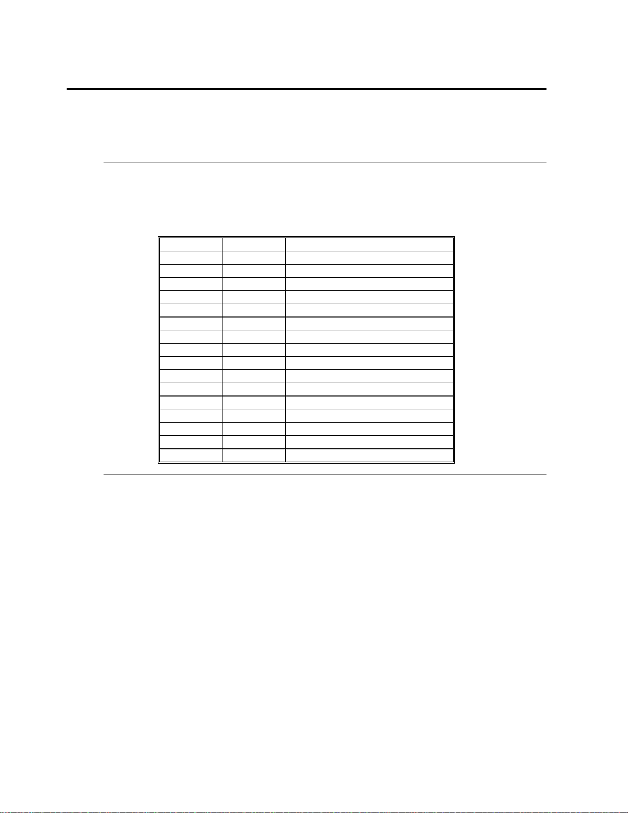
Priority Label Typical Interrupt Source
1 IRQ 0 Interval Timer 1, Counter 0 OUT
2IRQ 1Keyboard
3-10 IRQ 2 Used internally for IRQ 8 through IRQ 15
3 IRQ 8 R eal-TIme-Clock
4 IRQ 9 EISA bus
5 IRQ 10 EISA bus
6 IRQ 11 EISA bus
7 IRQ 12 PS/2 Mouse
8 IRQ 13 Coprocessor Error
9 IRQ 14 EISA bus (Hard disk drive controller)
10 IRQ 15 EISA bus
11 IRQ 3 Onboard serial port or EISA bus
12 IRQ 4 Onboard serial port or EISA bus
13 IRQ 5 Onboard parallel port or EISA bus
14 IRQ 6 Onboard floppy controller or EISA bus
15 IRQ 7 Onboard parallel port or EISA bus
Onboard I/O
The Enterprise-IV has an onboard IDE controller, floppy controller, two serial ports with National
Semiconductor 16450 UARTs, and a parallel port.
Chapter 2 Description

Specifications,
Continued
Timer Features
The Enterprise-IV has five programmable 16-bit counter/timers.
System Arbiter
The Enterprise-IV has standard EISA arbitration features.
Refresh Generation
The Enterprise-IV has a re fresh generation feature.
I/O Capability
The Enterprise-IV accesses 32-, 16-, or 8-bit memory devices and 32-, 16-, or 8-bit I/O devices on both the
VL-Bus and the EISA bus.
I/O Address Space
The Enterprise-IV uses I/O addresses x100h through x3FFh for ISA compatible I/O (x = a "don't care"
character which does not affect mapping location. For example, I/O port addresses 0100h, 1100h, 2100h,
and 3100h map to the same location).
The Enterprise-IV also uses the following EISA I/O port addresses:
•
•
•
•
s
000h through s0FFh for EISA expansion slot
s
400h through s4FFh for EISA expansion slot
s
800h through s8FFh for EISA expansion slot
s
C00h through sCFFh for EISA expansion slot
(s = EISA bus slot number, the motherboard is always 0)
Enterprise-IV EISA VLB Motherboard User's Guide

Specifications,
Continued
Memory Range
The Enterprise-IV uses 32-bit memory addresses to access 4 gigabytes of memory address space on the
EISA expansion slots.
I/O Channel Check
The Enterprise-IV supports the use of the I/O channel check to generate NMIs.
I/O Wait State Generation
The Enterprise-IV has an open bus structure (allowing multiple microprocessors to share system resources,
including memory). The Enterprise-IV supports refresh of system memory from channel microprocessors.
Keyboard and Keyboard Lock
The Enterprise-IV has a five-pin IBM AT-compatible DIN connector and has a keyboard lock to prevent
unauthorized access.
PS/2 Mouse
A PS/2 mouse can be used via a cable attached to a 10-pin berg mouse connector mounted next to the
keyboard connector.
Speaker
The Enterprise-IV has a standard speaker attachment.
Real Time Clock
The Enterprise-IV has a standard crystal-controlled AT-type real time clock. The real time clock is included
with ISA CMOS RAM on the Dallas DS1387 chip.
Chapter 2 Description

Chapter 3
Installation
Step Action Turn to
1 Unpack the motherboard Page 20
2 Set switch and jumper options. Page 22
3 Install memory. Page 25
4 Install upgradable processor or math coprocessor.
5 Install motherboard. Page 30
6 Connect the power supply. Page 32
7 Connect the keyboard. Page 35
8 Connect the mouse. Page 35
9 Connect cables. Page 36
10 Install adapter cards Page 41
11 Perform initial test and configuration. Page 47
Step 1 Unpack the Motherboard
Page Error!
Bookmark not
defined.
Step Action
1 If the box is damaged, call Technical Support at 404-246-
2 Perform all unpacking and installation procedures on a
3 The motherboard is packed in an anti-static bag, and
4 Place the motherboard on a grounded anti-static surface
5 Inspect the motherboard for damage. Do not apply power if
6 Press down on all socketed ICs to verify proper seating.
7 If the motherboard is undamaged, it is ready to be installed.
Chapter 3 Installation
8600.
grounded anti-static mat. Wear an anti-static wristband,
grounded at the same point as the anti-static mat or use a sheet
of conductive aluminum foil grounded through a 1 megohm
resistor.
sandwiched between sheets of sponge. Remove the sponge and
the anti-static bag. Save the original packing material.
component-side up.
damaged.

Enterprise-IV EISA VLB Motherboard User's Guide

Step 2 Set Switch and Jumper Options
CPU and Upgrade Socket
Intel 80486SX, 80486DX, or 8048DX2 CPUs can be inserted in the CPU socket. An Intel 80487SX math coprocessor or
an Upgrade Processor (P23T or P24T) can be inserted in the Upgrade Socket.
SW1
SW1 has two switches. See the graphic on the previous page for the SW1 location. Set SW1 before installation.
Switch Description
DIAG Turns on manufacturing diagnostics. This switch is factory-set to
COL/MONO Sets the video type. It has no effect if an EGA or VGA adapter is
J15, J16, J43 CPU Select
J15 (a four-pin berg), J16 (a three-pin berg), and J43 ( a two-pin berg) together select the CPU type.
OFF and should remain OFF.
used. It is factory-set to OFF ( for a monochrome display adapter).
Set ON to use a CGA video adapter card.
CPU in ZIF
Socket
None 486DX/SX OPEN N/A N/A
P23T,
487SX, or
P24T
P23T,
487SX, or
P24T
486DX or
486DX2
486DX or
486DX2
486SX N/A Short 2-3 N/A
486SX 486DX/SX SHORT Short 2-3 N/A
PQFP CPU J43 J15 J16
486DX/SX SHORT Short 1-2
Short 3-4
N/A Short 1-2
Short 3-4
N/A Short 1-2
Short 3-4
486DX/SX SHORT Short 1-2
Short 3-4
Short 2-3
Short 2-3
Short 1-2
Short 1-2
Chapter 3 Installation

Step 2 Set Switch and Jumper Options,
J15 Select CPU Type
J16 Select CPU Type
Continued
J43 Select CPU Type
Enterprise-IV EISA VLB Motherboard User's Guide

Step 2 Set Switch and Jumper Options,
Continued
J38 Local Bus ID
J38 is a three-pin single-inline berg. In normal operation, pins 1-2 are shorted when running Lo cal Bus Adapter Cards at 33
MHz or less (the default setting). Short pins 2-3 if running Local Bus Adapter Cards at speeds hi gher than 33 MHz.
J38 is shown below. Set J38 before installing the motherboard. See the graphic on the next page for the location of
J38.
J31 CPU Priority
J31 is a three-pin header that selects the CPU priority. Short pins 1-2 to set Low priority (the default setting). Short pins 2-
3 to set High priority.
Chapter 3 Installation

Step 3 Install Memory
The main memory on the Enterprise-IV EISA VLB motherboard consists of four 32-bit memory banks of one SIMM
socket each. The SIMM sockets accept 256 KB x 36, 1 MB x 36, 4 MB x 36, or 16 MB x 36 SIMMs in the
combinations shown below.
If used, SIMM banks must be completely filled, no matter which type of SIMMs are used. All SIMMs in a bank must be
the same type.
For system memory, fast page mode access and hidden refresh is supported. Burst support is provided.
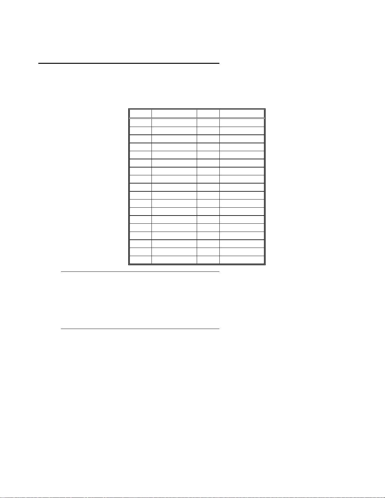
Possible Memory Configurations
Bank0 Bank1 Bank2 Bank3 Total RAM
256 KB x 36 None None None 1 MB
256 KB x 36 256 KB x 36 None None 2 MB
1 MB x 36 None None None 4 MB
256 KB x 36 256 KB x 36 1 MB x 36 None 6 MB
1 MB x 36 1 MB x 36 None None 8 MB
256 KB x 36 256 KB x 36 1 MB x 36 1 MB x 36 10 MB
1 MB x 36 1 MB x 36 1 MB x 36 None 12 MB
1 MB x 36 1 MB x 36 1 MB x 36 1 MB x 36 16 MB
4 MB x 36 None None None 16 MB
256 KB x 36 256 KB x 36 4 MB x 36 None 18 MB
1 MB x 36 4 MB x 36 None None 20 MB
1 MB x 36 1 MB x 36 4 MB x 36 None 24 MB
4 MB x 36 4 MB x 36 None None 32 MB
1 MB x 36 4 MB x 36 4 MB x 36 None 36 MB
1 MB x 36 1 MB x 36 4 MB x 36 4 MB x 36 40 MB
4 MB x 36 4 MB x 36 4 MB x 36 None 48 MB
4 MB x 36 4 MB x 36 4 MB x 36 4 MB x 36 64 MB
16 MB x 36 None None None 64 MB
16 MB x 36 16 MB x 36 None None 128 MB
16 MB x 36 16 MB x 36 16 MB x 36 None 192 MB
16 MB x 36 16 MB x 36 16 MB x 36 16 MB x 36 256 MB
Enterprise-IV EISA VLB Motherboard User's Guide

Step 3 Install Memory,
SIMM Part Numbers
Installing SIMMs
Continued
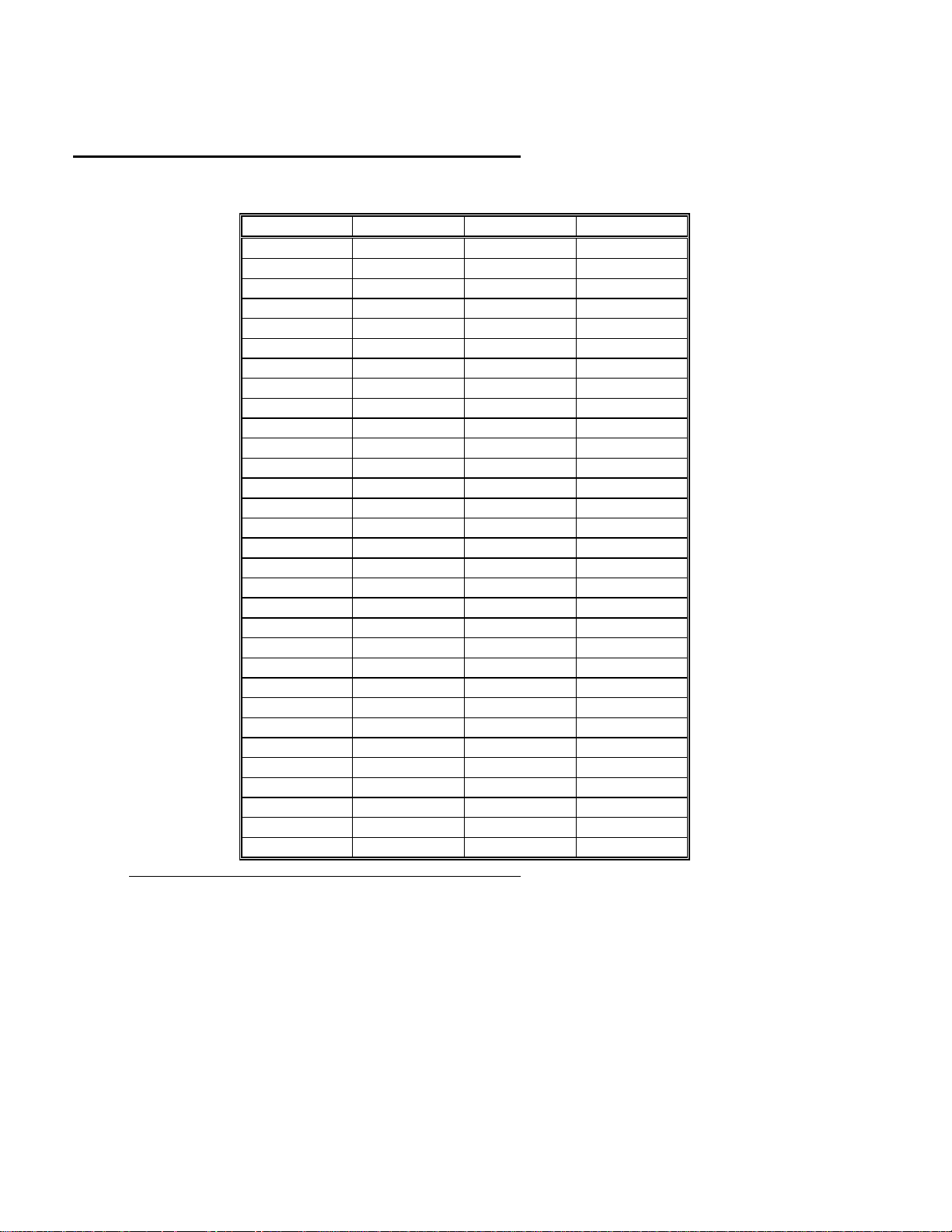
Memory Type Manufacturer Part Number
1 MB x 36 Micron MT12D136M-7
Mitsubishi MH1M36ADJ-7
PNY P361000-70
Motorola MCM36100AS-70
Oki MSC2355-70YS12
Samsung KMM5361000AV-7
4 MB x 36 Micron MT12D436M-7
Mitsubishi MH4M36SAJ-7
Motorola MCM36400S-70
PNY P364000-70
Samsung KMM5364100-7
16 MB x 36 Mitsubishi MH16M09J-7
Mitsubishi MH16M09TJ-7
Samsung KMM5916000-7
The system memory banks consist of four SIMM sockets. The sockets take 256 KB x 36, 1 MB x 36, 4 MB x 36, or 16
MB x 36 SIMMs. Use only one SIMM type to fill each bank.
Place the motherboard on an anti-static mat. With the component side of the SIMM facing you, firmly push the SIMM into
the socket. When properly inserted, the SIMM clicks in place as the latching pins engage, as shown below.
Chapter 3 Installation

Step 3 Install Memory,
Continued
Selecting SIMMs
The SIMMs must meet the following specifications:
Parameter Specification
Page Mode Fast
Refresh CAS before RAS
t
CAC
t
RAC
t
AA
t
RP
t
CPA
20 ns
≤
70 ns
≤
45 ns
≤
70 ns
45 ns
≤
Enterprise-IV EISA VLB Motherboard User's Guide

Step 4 Install Upgrade Processor
Follow the procedures described in this step to install an upgrade processor in the empty ZIF socket near the
CPU.
Improper Upgrade Processor installation can
damage the Upgrade Processor and/or the
motherboard. You must follow the procedures in
this section exactly as documented.
Processor Type and Speed
The Upgrade Processor socket is a 240-pin socket near one edge of the board. The Enterprise-IV VLB
EISA motherboard supports the following CPUs and Upgrade Processors:
Upgrade Processor in ZIF Socket PQFP CPU
None 486DX
P23T, 487SX, or P24T 486DX
P23T, 487SX, or P24T
486DX or 486DX2
486DX or 486DX2 486DX
486SX
486SX 486DX
Warning
The Enterprise-IV VLB EISA motherboard also supports future Intel processors and upgradeable
processors.
Chapter 3 Installation

Step 4 Install Upgrade Processor,
Installing an Upgrade Processor
The following discussion applies only to 169-pin processors, such as the 486DX, 486DX2, 486DX3,
486SX, 80487SX, P23T, or P24. Upgrade Processor installation is easy because a ZIF (zero insertion force)
socket is used.
Step Action
1 Lift the lever on the ZIF socket. The empty Upgrad e Processor sock et
looks like this.
2 Pin 1 of the socket has a white diagonal line across one corner on the
motherboard, which corresponds to pin 1 of the Upgrade Processor.
Check for bent pins on the Upgrade Processor chip. Gently straighten any
bent pins with pliers. Place the Upgrade Processor squarely in the middle
of the socket,
sides.
of the socket.
3 The Upgrade Processor socket is a 240-pin socket. But the 486DX,
486DX2, 486DX3, 486SX, 80487SX, P24, and P23T come in 169-pin
packages.
pins should show on all four sides of the socket,
making sure that one row of socket pins shows on all four
Make sure that pin 1 of the Upgrade Processor is aligned with pin 1
When these processors are installed, an extra row of socket
Continued
as shown below.
4 Complete installation by lifting the ZIF lever to the other side of the
socket, as shown below.
Enterprise-IV EISA VLB Motherboard User's Guide

Install Upgrade Processor,
Step Action
Continued
Installing a P24T
The P24T Upgrade Processor is a 240-pin package that uses all socket pins. Use the same procedure
describe above to install the P24T. However, when a P24T Upgrade Processor is properly installed, it uses
all 240 pins, so no extra socket pins can be seen.
Step 5 Install the Motherboard
The mounting holes on the motherboard are the same as an AT motherboard. Standoffs and mounting
screws should be supplied with the chassis.
Step Action
1 Wear an antistatic wristband. Place the chassis for the motherboard on an
anti-static mat.
2 Connect the chassis to ground to avoid static damage. Connect an
alligator clip with a wire lead to any unpainted part of the chassis. Ground
the other end of the lead to the same point as the mat and wristband.
3 Rotate the chassis so that the front is to the right, and the rear is to the left.
The side facing you is where the motherboard is mounted. The power
supply is mounted near the back end of the chassis.
4 Push four nylon standoffs from the solder side of the motherboard in the
holes provided for them. The standoffs lock in place.
5 Find the slots provided for the standoffs on the chassis. Hold the
motherboard, component-side up, with the edge with three standoffs
toward you and the edge with the power supply connector away from you.
The edge connectors for the adapter cards should be on the left.
6 Carefully slide the motherboard into the chassis. Make certain that the
standoffs fit the slots provided for them. If the standoffs are properly
locked, the motherboard should not slide. It should also rest level with the
chassis. The far edge should fit the slots in the plastic clips.
7 Place the two mounting screws in the holes provided for them and tighten
them. If necessary, shift the motherboard slightly to align the mounting
holes on the motherboard with the holes on the chassis.
Be sure to use plastic standoffs.
Chapter 3 Installation


The motherboard mounting hole locations are shown below.
egend:
! screw hole" Mounting hole
Enterprise-IV EISA VLB Motherboard User's Guide

Step 6 Connect the Power Supply
The power supply should match the physical configuration of the chassis. Make sure that the power switch
is Off before assembly.
Before attaching the power cables, make sure that the proper voltage is selected. Power supplies often can
run on a wide range of voltages, but must be set (usually with a switch) to the proper range. Use at least a
230 watt power supply that has built-in filters to suppress radiated emissions. If all EISA expansion slots are
filled, a standard 200-250 watt power supply is not sufficient, a 300-450 watt power supply is needed. The
location of the power supply connectors (P1, P2, and P3) is shown in the following graphic.
Connect to P1 and P2
The connector with three red wires and two black wires is attached to P2. The connector with the Orange
line 1 is attached to P1. P3 is provided for high capacity power supplies that have an extra cable. The
following graphic shows the wire colors for all power connectors.
Chapter 3 Installation

Step 6 Connect the Power Supply,
Continued
Power Supply Connectors are Keye d
Power supply connectors are keyed to make sure you attach them correctly. The keys must be cut to fit on
some power supplies, as shown below.
Enterprise-IV EISA VLB Motherboard User's Guide

Step 6 Connect the Power Supply,
P1 Pinout
Pin Description
1 Power Good (Orange wire)
2 VCC (Red wire)
3 +12 Volts (Yellow wire)
4 -12 Volts (Blue wire)
5 Ground (Black wire)
6 Ground (Black wire)
P2 Pinout
Pin Description
1 Ground (Black wire)
2 Ground (Black wire)
3 -5 Volts (White wire)
4 VCC (Red wire)
5 VCC (Red wire)
6 VCC (Red wire)
Continued
P3 Pinout
Pin Description
1 VCC (Red wire)
2 VCC (Red wire)
3 VCC (Red wire)
4 Ground (Black wire)
5 Ground (Black wire)
6 Ground (Black wire)
Chapter 3 Installation

Step 7 Connect the Keyboard
The keyboard connector is a five-pin DIN socket (see below) labeled KEYBRD and J8 on the motherboard.
It accepts a standard ISA keyboard.
Step 8 Connect the Mouse
Pin Assignments
1 Keyboard clock
2 Keyboard data
3Not used
4 Ground
5VCC
The American Megatrends Enterprise-IV EISA VLB motherboard mouse connector is a 10-pin berg
connector.
J11 is a 10-pin berg connector that attaches to a PS/2-compatible mouse via a standard serial cable. The
mouse connector is next to the keyboard connector. The connector position is shown above. The J11 pinout
and J11 are shown below.
Pin Assignment Pin Assignment
1Clock2 N/C
3N/C4N/C
5N/C6FVCC
7N/C8Data
9GNDN/AKey Pin
Enterprise-IV EISA VLB Motherboard User's Guide

Step 9 Connect Cables
When attaching connectors to the motherboard, make sure you attach the correct end. Most connector wires
are color-coded. Match the color of the wires leaving pin 1 on the switch or LED to pin 1 on the connector
end. There may be more than one connector with the same color-coded wires. If so, follow the wire to the
switch or LED. Pin 1 of all connectors is labeled on the motherboard. Sometimes the label is obscured by a
part. You can always identify Pin 1 by looking at the other side of the motherboard. All Pin 1 locations are
always identified by a square pad.
Summary of Connectors
• Reset Switch cable to J41,
• Speaker cable to J40,
• Keyboard Lock cable to J34,
• Turbo LED cable to J42,
• Turbo switch cable to J39, and
• J5 IDE Hard Disk Drive LED.
The DIAG Led is mounted n the motherboard.
J41 Reset Switch Connector
J41 is a two-pin single-inline berg. A hard reset is performed by the system when the Reset switch is
pressed. Pin 1 is ground and Pin 2 is Hard Reset. The graphic above shows the location of J41. The
following is an illustration of J41.
Chapter 3 Installation

Step 9 Connect Cables,
Continued
J40 Speaker Connector
J40 is a four-pin single-inline berg. See the graphic at the top of the page for the J40 location. J40 is shown
below.
Pin Description
1 Data Out
2Key
3 Ground
4VCC
J34 Keyboard Lock Connector
J34 is a five-pin single-inline berg that connects via a cable to the keyboard lock. The keyboard lock allows
you to lock the keyboard, protecting the system from unauthorized use. Pin 1 of J34 on the motherboard is
labeled. The connector and the J34 pinout is shown below. See the graphic at the top of the previous page
for the J34 location.
Enterprise-IV EISA VLB Motherboard User's Guide
Pin Description
1 LED power
2 Key
3 Ground
4 Keyboard Lock
5 Ground

Step 9 Connect Cables,
Continued
J42 Turbo LED Connector
J42 is a two-pin berg that connects to the Turbo LED via a cable. The LED lights when the board runs at
high speed. Connect the Turbo LED to J42. J42 is shown below. See the graphic at the top of page 36 for
the J42 location.
J39 Turbo Switch Connector
J39 is a two-pin berg that connects to the turbo switch mounted on the chassis via a cable, as shown below.
The turbo LED switch is bipolar. You can select Low or High speed by pressing the turbo switch, attached
to J39 via a connector cable. J39 is shown below. See the graphic at the top of page 36 for the J39 location.
Chapter 3 Installation

Enterprise-IV EISA VLB Motherboard User's Guide

Step 10 Install Adapter Cards
The Enterprise – IV EISA VLB motherboard has seven expansion slots numbered SLOT – SLOT7.
.
Chapter 3 Installation

Step 10 Install Adapter Cards
Type of Adapter Card Slots
Bus Mastering
VL-Bus
Cards
EISA 32-bit
EISA 32-bit Non-Bus Mastering Cards Slot 7
Standard 8-bit XT- and 16-bit AT-compatible
Cards
EISA Adapter Cards
EISA adapter cards have different fingers on the edge connecters than ISA adapter cards. The EISA
expansion slots have two rows of contacts, one below the other. AN ISA (AT-compatible) Adapter Card can
be inserted into the EISA connector only far enough to make contact with the upper row of contacts. T he
longer fingers on EISA adapter cards allow contact with the second row of contacts. See the following
graphic.
Bus Mastering
32-bit Local Bus Adapter
Cards Slots 1 - 6
Slots 6 and 7
Slots 1 - 7
When installing EISA adapter cards, make sure that they snap in twice and are fully seated in the EISA
expansion slot. If the card makes contact only with the upper row of contacts, it cannot function properly.
Enterprise-IV EISA VLB Motherboard User's Guide

Step 10 Install Adapter Cards,
8-Bit ISA Slot Pinout
Pin Use Pin Use
A1 IOCHCK- B1 GND
A2 SD07 B2 RSTDRV
A3 SD06 B3 +5
A4 SD05 B4 IRQ9
A5 SD04 B5 -5
A6 SD03 B6 DREQ2
A7 SD02 B7 -12
A8 SD01 B8 OWS-
A9 SD00 B9 +12
A10 IOCHRDY B10 GND
A11 AEN B11 SMEMWA12 SA19 B12 SMEMRA13 SA18 B13 IOWA14 SA17 B14 IORA15 SA16 B15 DACK3A16 SA15 B16 DREQ3
A17 SA14 B17 DACK1A18 SA13 B18 DREQ1
A19 SA12 B19 REFA20 SA11 B20 SYSCLK
A21 SA10 B21 IRQ7
A22 SA09 B22 IRQ6
A23 SA08 B23 IRQ5
A24 SA07 B24 IRQ4
A25 SA06 B25 IRQ3
A26 SA05 B26 DACK2A27 SA04 B27 T/C
A28 SA03 B28 BALE
A29 SA02 B29 +5
A30 SA01 B30 OSC
A31 SA00 B31 GND
Continued
Chapter 3 Installation
Step 10 Install Adapter Cards,
Continued
16-Bit ISA Extension Pinout
The following 16-bit pins are an extension of the 8-bit board layout and are used in conjunction with the 8bit board standard pins.
Pin Use Pin Use
C1 SBHE- D1 MEMCS16C2 LA23 D5 IOCS16C3 LA22 D3 IRQ10
C4 LA21 D4 IRQ11
C5 LA20 D5 IRQ12
C6 LA19 D6 IRQ13
C7 LA18 D7 IRQ14
C8 LA17 D8 DACK0-
C9 MEMR- D9 DREQ0
C10 MEMW- D10 DACK5C11 SD08 D11 DREQ5
C12 SD09 D12 DACK6C13 SD10 D13 DREQ6
C14 SD11 D14 DACK7C15 SD12 D15 DREQ7
C16 SD13 D16 +5
C17 SD14 D17 MASTERC18 SD15 D18 GND
32-bit EISA Slot Pinout
The following table identifies the pin values for the pins on each of the eight rows of pins on an EISA
adapter card. 8- and 16-bit ISA signals are shown. Pins labeled
on the bus from adjacent power pins. Rows A, B, C, and D are upper (ISA) contacts. Rows E, F, G, and H
are lower (EISA) contacts. The following table lists the pinouts for Rows F, B, E, and A.
Enterprise-IV EISA VLB Motherboard User's Guide
xxxxxx
are generally used to isolate signals
Step 10 Install Adapter Cards,
Continued
32-bit EISA Slot Pinout
Row F Row B Row E Row A
1 GND 1 GND 1 CMD# 1 IOCHK#
2 + 5 volts 2 RESDRV 2 START# 2 D7
3 + 5 volts 3 + 5 volts 3 EXRDY 3 D6
xxxxxx
4
xxxxxx
5
6 Access Key 6 DRQ 2 6 Access Key 6 D3
xxxxxx
7
xxxxxx
8
9 + 12 volts 9 + 12 volts 9 MSBURST# 9 D0
10 M-IO 10 GND 10 W-R 10 CHRDY
11 LOCK# 11 SMWTC# 11 GND 11 AEN
12 Reserved 12 SMRDC# 12 Reserved 12 SA19
13 GND 13 IOWC# 13 Reserved 13 SA18
14 Reserved 14 IORC# 14 Reserved 14 SA17
15 BE# 3 15 DAK# 3 15 GND 15 SA16
16 Access Key 16 DRQ3 16 Access Key 16 SA15
17 BE# 2 17 DAK# 1 17 BE# 1 17 SA14
18 BE# 0 18 DRQ1 18 LA# 31 18 SA13
19 GND 19 REFRESH# 19 GND 19 SA12
20 + 5 volts 20 BCLK 20 LA# 30 20 SA11
21 LA# 29 21 IRQ 7 21 LA# 28 21 SA10
22 GND 22 IRQ 6 22 LA# 27 22 SA9
23 LA# 26 23 IRQ 5 23 LA# 25 23 SA8
24 LA# 24 24 IRQ 4 24 GND 24 SA7
25 Access Key 25 IRQ 3 25 Access Key 25 SA6
26 LA16 26 DAK# 2 26 LA15 26 SA5
27 LA14 27 T-C 27 LA13 27 SA4
28 + 5 volts 28 BALE 28 LA12 28 SA3
29 + 5 volts 29 + 5 volts 29 LA11 29 SA2
30 GND 30 OSC 30 GND 30 SA1
31 LA10 31 GND 31 LA9 31 SA0
, cont'd
4 IRQ 9 4 EX32# 4 D5
5 - 5 volts 5 GND 5 D4
7 - 12 volts 7 EX16# 7 D5
8 NOWS# 8 SLBURST# 8 D1
Chapter 3 Installation

Step 10 Install Adapter Cards,
Continued
32-bit EISA Slot Pinout
Row H Row D Row G Row C
1 LA8 1 M16# 1 LA7 1 SBHE#
2 LA6 2 IO16# 2 GND 2 LA23
3 LA5 3 IRQ 10 3 LA4 3 LA22
4 + 5 volts 4 IRQ 11 4 LA3 4 LA21
5 LA2 5 IRQ 12 5 GND 5 LA20
6 Access Key 6 IRQ 15 6 Access Key 6 LA19
7 D16 7 IRQ 14 7 D17 7 LA18
8 D18 8 DAK# 0 8 D19 8 LA17
9 GND 9 DRQ 0 9 D50 9 MRDC#
10 D51 10 DAK# 5 10 D52 10 MWTC#
11 D53 11 DRQ 5 11 GND 11 D8
12 D54 12 DAK# 6 12 D55 12 D9
13 GND 13 DRQ# 6 13 D56 13 D10
14 D57 14 DAK# 7 14 D58 14 D11
15 Access Key 15 DRQ# 7 15 Access Key 15 D12
16 D59 16 + 5 volts 16 GND 16 D13
17 + 5 volts 17 MASTER16# 17 D30 17 D14
18 + 5 volts 18 GND 18 D31 18 D15
19 MAXx# 19 MREQx#
, cont'd
VL-Bus Cards
VL-Bus cards use the standard ISA/EISA connectors, but they also have an additional 112-pin MCA
connector inline with the EISA expansion card sockets, as shown below.
Enterprise-IV EISA VLB Motherboard User's Guide

Step 10 Install Adapter Cards,
Continued
VL-Bus
The two longest expansion slots on the Enterprise-IV EISA VLB motherboard are for VL-Bus adapter
cards. These VL-Bus
2).
These slots use the standard EISA/ISA sockets and an inline 112-pin extension connector to
bus mastering
slots are labeled
VESA MASTER SLOT-1)
VESA MASTER SLOT-
and
accommodate VL-Bus-compatible adapter cards. The pinout for the VL-Bus connector follows:
Pin Use Pin Use
A1 DAT01 B1 DAT00
A2 DAT03 B2 DAT02
A3 GND B3 DAT04
A4 DAT05 B4 DAT06
A5 DAT07 B5 DAT08
A6 DAT09 B6 GND
A7 DAT11 B7 DAT10
A8 DAT13 B8 DAT12
A9 DAT15 B9 VCC
A10 GND B10 DAT14
A11 DAT17 B11 DAT16
A12 VCC B12 DAT18
A13 DAT19 B13 DAT20
A14 DAT21 B14 GND
A15 DAT23 B15 DAT22
A16 DAT25 B16 DAT24
A17 GND B17 DAT26
A18 DAT27 B18 DAT28
A19 DAT29 B19 DAT30
A20 DAT31 B20 VCC
A21 ADR30 B21 ADR31
A22 ADR28 B22 GND
A23 ADR26 B23 ADR29
A24 GND B24 ADR27
A25 ADR24 B25 ADR25
Chapter 3 Installation

Step 10 Install Adapter Cards,
Continued
VL-Bus
Pin Use Pin Use
A26 ADR22 B26 ADR23
A27 VCC B27 ADR21
A28 ADR20 B28 ADR19
A29 ADR18 B29 GND
A30 ADR16 B30 ADR17
A31 SA00 B31 GND
A32 ADR12 B32 VCC
A33 ADR10 B33 ADR13
A34 ADR08 B34 ADR11
A35 GND B35 ADR09
A36 ADR06 B36 ADR07
A37 ADR04 B37 ADR05
A38 WBACK# B38 GND
A39 BE0# B39 ADR03
A40 VCC B40 ADR02
A41 BE1# B41 N/C
A42 BE2# B42 RESET#
A43 GND B43 D/C#
A44 BE3# B44 M/IO#
A45-47 A05# B45-47 W/R#
A48 LRDY# B48 RDYRTN#
A49 LDEV<># B49 GND
A50 LREQ<># B50 IRQ9
A51 GND B51 BRDY#
A52 LGNT<># B52 BLAST#
A53 VCC B53 ID0
A54 ID5 B54 ID1
A55 ID3 B55 GND
A56 ID4 B56 LCLK
A57 LKEN# B57 VCC
A58 LEADS# B58 LBS16#
, cont'd
Step 11 Perform Initial Test and Configuration
Before powering up the system, make sure that:
_ all adapter cards are seated properly,
_ all connectors are properly seated,
_ th e math coprocessor or Upgradable Processor is seated properly,
_ there are no screws or other foreign material on the motherboard,
_ the system is plugged into a surge-protected power strip, and
_ blank back panels are installed on the back of the chassis to minimize RF emissions.
Enterprise-IV EISA VLB Motherboard User's Guide

Step 11 Perform Initial Test and Configuration,
Continued
Start the Test
Plug everything in and turn on the switch. If there are any problems, turn off the unit immediately. Reinstall
the connectors and call Technical Support at 404-246-8600.
Configure the System
Run AMIBIOS Setup to save configuration data in CMOS RAM. The system then resets, runs POST, and
boots the operating system. See page 63 for a description of STANDARD CMOS SETUP configuration
options. If the system operates normally, a memory display should appear on the monitor. The BIOS Power
On Self Test (POST) should run. POST beeps or displays error messages is unsuccessful. There is a serious
problem if the system beeps. The beeps are part of a Beep Code (see page 50) that indicates a bad
component. Make sure the affected part is properly seated and connected. If the BIOS is able to initialize
the system video monitor, messages (described on page 51) are displayed on the screen.
Run the ECU
Run the American Megatrends EISA Configuration Utility (ECU) to properly configure the system. Use the
files on the diskette supplied with the Enterprise-IV EISA VLB motherboard (!AMI87A1.CFG and
AMI87A1.OVL). The
American Megatrends EISA Configuration Utility User's Guide
provides complete
details about running the ECU.
Chapter 3 Installation

Chapter 4
AMIBIOS Power-On Self Test
AMIBIOS provides all IBM-standard POST routines as well as enhanced POST routines. POST supports
CPU internal diagnostics. POST codes are accessible via the Manufacturing Test Port (I/O Port 80h).
POST Phases
When the system is powered on, AMIBIOS executes POST routines. The POST phases are:
System Test and Initialization
(test and initialize motherboards for normal operations) and
System Configuration Verification
BIOS Error Reporting
(compare defined configuration with hardware actually installed).
If... then...
the error occurs before the
display device is initialized,
the error occurs after the
display device is initialized,
a series of beeps sound. Beep codes indicate that a
fatal error occurred. The Beep Codes a re described
on the next page.
the error message is displayed. Displayed BIOS
error messages are explained on page 51. A prompt
to press <F1> can also appear with displayed error
messages.
Enterprise-IV EISA VLB Motherboard User's Guide

Beep Codes
Fatal errors, listed below, are communicated through a serie s of audible beep s. All errors excep t Beep Code
8 are fatal. Fatal errors halt the boot process.
In most cases, displayed errors allow the system to continue. AMIBIOS displayed errors are described on
page 51.
Beeps Error message Description
1 Refresh Failure The memory refresh circuitry on the
2 Parity Error A parity error was detected in the base memory
3 Base 64 KB Memory
Failure
4 Timer Not Operationa l A memory failure occurred within the first 64
5 Processor error The CPU generated an error.
6 8042 - Gate A20
Failure
7 Processor Exception
Interrupt Error
8Display Memory
Read/Write Error
9 ROM Checksum Error The ROM checksum does not match the value
10 CMOS Shutdown
Register Read/Write
Error
11 Cache memory bad —
do not enable cache
motherboard is faulty.
(the first 64 KB block) of memory.
Memory failure in first 64 KB.
KB of memory. Or Timer 1 on the motherboard
is not functioning.
Gate A20 on the keyboard controller (8042)
allows the CPU to operate in p r otected mode.
The BIOS is not able to switch the CPU to
protected mode.
The CPU generated an exception interrupt.
The system video adapter is either missing or
its memory is faulty. This is not a fatal error.
encoded in the BIOS.
The shutdown register for CMOS RAM failed.
The cache memory test failed. Cache memory
is disabled.
Chapter 4 AMIBIOS POST

Troubleshooting System Problems
What to Do If the Computer Beeps
Here is what you need to do if your computer has an AMIBIOS and it starts beeping:
If the system beeps... then...
1, 2, or 3 times... reseat the memory SIMMs or DIPs. If the system
6 times... reseat the keyboard controller chip. If it still beeps,
8 times... there is a memory error on the video adapter.
9 times. .. the BIOS chip is b ad. The system probably need s a
11 times... reseat the cache memory on the motherboard. If it
4, 5, 7, or 10 times... the motherboard must be replaced.
still beeps , replace th e memory.
replace the keyboard controller. If it still beeps, try
a different keyboard, or replace the keyboard fuse,
if the keyboard has one.
Replace the video adapter, or the RAM on the vi deo
adapter.
new BIOS ROM chip.
still beeps, replace the cache memory.
AMIBIOS Displayed Error Messages
Error message are displayed as follows:
ERROR Message Line 1
ERROR Message Line 2
Press the <F1> key to continue
After the message, the system halts. The system does not halt if
ADVANCED CMOS SETUP is set to
Error Message Explanation
8042 Gate-A20
Error
Address Line
Short!
C: Drive Error Drive C: may be missing. Run the BIOS Hard Disk Utility.
C: Drive Failure No response from hard disk drive C:. Replace drive C:.
Cache Memory
Bad, Do Not
Enable Cache!
CH-2 Timer Error Error in timer 2.
CMOS Battery
State Low
Disabled.
Gate A20 on the keyboard controller (8042) is not working.
Replace the 8042.
Error in the address decoding circuitry on the motherboard.
Check the C: hard disk type in STANDARD CMOS SETUP.
Cache memory on the motherboard is defective. Test cache
memory with AMIDiag.
CMOS RAM is powered by a battery. The battery power is
low. Replace the battery.
Wait for <F1> If Any Error
in
Enterprise-IV EISA VLB Motherboard User's Guide

AMIBIOS Displayed Messages,
Error Message Explanation
CMOS Checksum
Failure
CMOS System
Options Not Set
CMOS Display
Type Mismatch
CMOS Memory
Size Mismatch
CMOS Time &
Date Not Set
D: Drive Error No response from hard disk drive D:. Drive D: may be
D: drive failure No response from hard disk drive D:. Replace drive D:.
Diskette Boot
Failure
Display Switch
Not Proper
DMA Error Error in the DMA controller on the motherboard.
DMA #1 Error Error in the first DMA channel on the motherboard.
DMA #2 Error Error in the second DMA channel on the motherboard.
FDD Controller
Failure
HDD Controller
Failure
INTR #1 Error Interrupt channel 1 failed POST.
INTR #2 Error Interrupt channel 2 failed POST.
Invalid Boot
Diskette
Keyboard Is
Locked...Unlock
It
Keyboard Error Timing problem with the keyboard. Set
KB/Interface
Error
No ROM BASIC Cannot find a proper bootable sector on either drive A: or hard
Off Board Parity
Error
On Board Parity
Error
Continued
After CMOS RAM settings are saved, a checksum is
generated. This message appears if the previous checksum
differs from the current checksum. Run AMIBIOS Setup.
The values st or ed in CMOS RAM are either corrupt or
nonexistent. Run AMIBIOS Setup.
The video type in CMOS RAM does not match the type
detected by the BIOS. Run AMIBIOS Setup.
The amount of memory on the motherboard is different than
the amount in CMOS RAM. Run AMIBIOS Setup.
Run STANDARD CMOS SETUP to set the date and time in
CMOS RAM.
missing. Run the AMIBIOS Hard Disk Utility. Check the D:
hard disk type in STANDARD CMOS SETUP.
The boot disk in floppy drive A: is corrupt. It cannot be used to
boot the system. Use another boot disk and follow the screen
instructions.
Some systems require a video switch on the motherboard be
set to either color or monochrome. Turn the system off, set the
switch properly, then power on.
The BIOS cannot communicate with the floppy controller.
Check all connections after the system is powered down.
The BIOS cannot communicate with the hard disk controller.
Check all connectors after the system is powered down.
The BIOS can read the diskette in floppy drive A:, but it
cannot boot the system with it. Use another boot diskette and
follow the screen instructions.
The keyboard lock on the syst em is engaged. The system must
be unlocked to continue the boot process.
Keyboard
STANDARD CMOS SETUP to
keyboard POST routines.
Error in the keyboard connector on the motherboard.
disk drive C:. ROM Basic (INT 18h) does not run. The BIOS
cannot find ROM Basic.
Parity error in adapter card memory. The format is:
OFF BOARD PARITY ERROR ADDR (HEX) = (XXXX)
XXXX
is the hex address where the error occurred. Run
AMIDiag to find memory errors.
Parity error in motherboard memory. The format is:
ON BOARD PARITY ERROR ADDR (HEX) = (XXXX)
XXXX
is the hex address where the error occurred. Run
Not Installed
in
to skip the
Chapter 4 AMIBIOS POST

AMIBIOS Displayed Messages,
Error Message Explanation
Parity Error ???? Parity error in system memory but the address cannot be
EISA AMIBIOS Error Messages
Error Message Explanation
EISA CMOS Checksum
Failure
EISA CMOS inoperational Read/Write error in extended CMOS RAM. The
Expansion Board not ready at
X, Y, Z
Slot
Fail-Safe Timer NMI
Inoperational
ID information mismatch for
X, Y, Z
Slot
Invalid Configuration
Information for Slot X, Y, Z.
Software Port NMI
Inoperational
.
Continued
AMIDiag to find memory errors.
determined. Run AMIDiag to fin memory errors.
The Checksum for EISA CMOS is incorrect.
Replace the EISA Extended CMOS RAM battery.
battery may need to be replaced.
Cannot find the adapter card in Slot
Make sure the adapter card is in the correct slot and
is seated correctly.
Devices that depend on the fail-safe NMI timer will
not operate correctly.
The ID of the EISA Adapter Card in Slot
does not match the ID in EISA CMOS RAM.
The configuration information for EISA Adapter
X, Y
Cards
this slot cannot be configured. Run the ECU.
The software port NMI is not working.
, or Z is not correct. The adapter card in
X, Y
, or Z.
X, Y
, or
Z
Enterprise-IV EISA VLB Motherboard User's Guide

NMI Messages
EISA NMI Message s
ISA NMI Messages
EISA NMI Message Explanation
BUS Timeout NMI at Slot
(E)nable (D)isable Expansion
Board?
Expansion Board Disabled at
n
Slot
n
Bus Timeout NMI at Slot n.
Type E to enable the adapter card that had an
NMI or D to disable it.
The adapter card in Slot n is disabled.
Expansion Board NMI at Slot nAn expansion board NMI occurred in Slot n.
Fail-Safe Timer NMI Fail-safe timer NMI generated.
Software Port NMI Software port NMI generated.
NMI Message Explanation
Memory Parity
xxxxx
Error at
I/O Card Parity
xxxxx
Error at
Memory failed. If the memory location is known, it is
displayed as
Error ????
xxxxx
. If not, the message is
.
Memory Parity
An adapter card failed. If the address is known, it is
displayed as
Error ????
xxxxx
. If not, the message is
.
I/O Card Parity
DMA Bus Time-out A device drove the bus signal for more than 7.8 µseconds.
BIOS Configuration Summary Screen
AMIBIOS System Configuration (C) 1985-1993 American Megatrends Inc.
Main Processor
Numeric Processor
Floppy Drive A:
Floppy Drive B:
Display Type:
AMIBIOS Date:
80486DX2 - 50MHz CPU
256 KB CACHE MEMORY
Chapter 4 AMIBIOS POST
: 486DX2
: Present
: 1.2 MB 5½
: 1.44 MB 5¼
: VGA/PGA/EGA
: 11/11/92
Base Memory Size
Ext. Memory Size
Hard Disk C: Type
Hard Disk D: Type
Serial Port(s)
Parallel Port(s)
: 640 KB
: 15360 KB
: 44
: None
: 3F8
: 378

AMIBIOS Identification Strings
The AMIBIOS Identification String is displayed at the bottom of the screen during the memory test. You
will need this string when reporting AMIBIOS problems.
AMIBIOS (C) 1993 American Megatrends Inc.,
BIOS Release xxxxxxxx
XXXXX
KB OK
Press <DEL> if you want to run SETUP
(C) American Megatrends Inc.,
41-0000-004687-00111111-111192-AMIS87-H
Enable the
Wait for <F1> If any Error
option in ADVANCED CMOS SETUP, then press <Ins> to display
two additional AMIBIOS Identification Strings.
Step Action
1 When a problem occurs, freeze the screen b y powering on the
system and holding a key down on the keyboard.
2 Copy the BIOS ID Strings on a sheet of paper before calling
American Megatrends technical support at 404-246-8600.
3 Press <F1> to continue the boot process.
4
is displayed. You can press <Del> to access AMIBIOS Setup.
Hit <DEL> if you want to run SETUP
Enterprise-IV EISA VLB Motherboard User's Guide


Chapter 5
AMIBIOS Setup
Keyboard Speed Switching
You can increase processor speeds at any time by pressing <Ctrl> <Alt> <+>. Processor speed can be
decreased by pressing <Ctrl> <Alt> <->.
Of course, the OEM can modi fy these ke ystro ke combinations through AMIBCP. The above settings are the
default settings.
Cache Memory Enable
You can enable both internal and external cache memory by pressing <Ctrl> <Alt> <Shift> <+>. You can
disable cache memory by pressing <Ctrl> <Alt> <Shift> <->.
Of course, the OEM can modi fy these ke ystro ke combinations through AMIBCP. The above settings are the
default settings.
AMIBIOS Setup Parts
AMIBIOS Setup is divided into three parts:
• STANDARD CMOS SETUP,
• ADVANCED CMOS SETUP, and
• ADVANCED CHIPSET SETUP.
Enterprise-IV EISA VLB Motherboard User's Guide

Running AMIBIOS Setup,
Continued
STANDARD CMOS SETUP
AMIBIOS STANDARD CMO S SETUP, discusse d in Section 2 beginning on page 63, confi gures system
components such as floppy drives, hard disk drives, monitor type, and the keyboard.
ADVANCED CMOS SETUP
ADVANCED CMOS SETU P, discussed in Section 3 beginning on page 67, configures t he system
password, keyboard typematic rate, boot sequence and speed, and enables system performance features,
such as Fast Gate A20 support.
ADVANCED CHIPSET SETUP
ADVANCED CHIPSET SETUP confi gures chipset-specific options. It is d iscussed in Section 4, beginning
on page 77.
Chapter 5 AMIBIOS Setup

Section 1
Running AMIBIOS Setup
AMIBIOS Setup resides in ROM and is available when the computer is turned on. AMIBIOS Setup permits
the end user to configure these system parameters (type of disk drives and monitor, day, date, and time, and
so on). The parameters are stored in CMOS RAM. When the computer is turned off, a back-up battery
provides power to CMOS RAM, which retains these parameters. The system is configured with these values
when powered on.
Default Values
If the configuration values in CMOS RAM become corrupted, the system is configured with the default
settings stored in this ROM file. There are two sets of BIOS settings stored in the ROM file: the BIOS
Setup defaults and the Power-On defaults. See page 61 for more information on default settings.
Starting AMIBIO S Setup
When POST completes, the following appears:
Hit <DEL> if you want to run SETUP
Press <Del> to run AMIBIOS Setup.
Warning Message
A warning is displayed when STANDARD CMOS SETUP, ADVANCED CMOS SETUP, or
ADVANCED CHIPSET SETUP is selected. Press <Enter> to display the next screen.
Enterprise-IV EISA VLB Motherboard User's Guide

AMIBIOS Setup Keys
Keystroke Action
<Esc> Returns to previous screen.
→, ←, ↓, ↑
<PgUp> and
<PgDn>;
<Ctrl><PgUp>
and
<Ctrl><PgDn>
<F1> Displays Help.
<F2> Change background colors.
<F3> Change foreground colors.
<F5> Restores the settings resident when the current Setup session
<F6> Loads all options in ADVANCED CMOS SETUP and
<F7> Loads all options in ADVANCED CMOS SETUP and
<F10> Saves all changes made to Setup and returns to DOS.
Move the cursor from one option to t he next.
Modify the default setting of the options for the highlighted
parameter. If there are fewer than 10 options, <Ctrl> <PgUp>
and <Ctrl> <PgDn> operate like <PgUp> and <PgDn>.
began. These settings are taken from CMOS RAM if CMOS
RAM was uncorrupted at the start of the session. Otherwise,
the BIOS Setup default settings are used.
ADVANCED CHIPSET SETUP with the BIOS Setup default s .
ADVANCED CHIPSET SETUP with the Power-On defaults.
Note:
The default settings for <F5>, <F6>, and <F7> is always N. To execute these options, change the
N
to Y and press <Enter>.
AMIBIOS Setup Main Menu
Chapter 5 AMIBIOS Setup

Auto Configuration With BIOS Defaults
Auto Configuration With BIOS Defaults uses the default system settings for all AMIBIOS Setup options.
The BIOS defaults are best-case settings that optimize system performance. If CMOS RAM is corrupted,
the BIOS default settings are automatically loaded. Highlight this option, type Y, and press <Enter> to use
BIOS defaults. The following appears:
Default values loaded. Press any key to continue.
Auto Configuration With Power-On Defaults
This option configures the Power-On default settings for all AMIBIOS Setup options. These are not optimal
for system performance, but are the most stable settings. Use this option as a diagnostic aid if the system is
erratic. Highlight this option, type Y, and press <Enter> to use the Power-On defaults. The following
appears:
Default values loaded. Press any key to continue.
Change Password
The AMIBIOS password feature provides password control over the use of AMIBIOS Setup and the system
itself.
Enterprise-IV EISA VLB Motherboard User's Guide

AUTO DETECT HARD DISK
When enabled, this option displays the parameters for IDE hard disk drives. You can accept or reject the
parameters. If accepted, these parameters are displayed in STANDARD CMOS SETUP. The parameters
are displayed as follows:
Write to CMOS and Exit
The selected options and new password (if any) are stored in CMOS RAM. A checksum is calculated and
written to CMOS RAM. Control is passed to AMIBIOS.
Write to CMOS and Exit (Y/N)?
appears when you pre ss <Enter> when this option is highlighted. Type N and press <Enter> to return to the
Main Menu. Type Y and press <Enter> to save the system parameters and continue the boot process.
Do Not Write to CMOS RAM and Exit
This option passes control to AMIBIOS. After this option is highlighted and you press <Enter>, type N and
press <Enter> to return to the Main Menu. Type Y and press <Enter> to continue to boot without saving.
Chapter 5 AMIBIOS Setup

Section 2
STANDARD CMOS SETUP
STANDARD CMOS SETUP is the first option on the Main Menu. Press <Enter> when
CMOS SETUP
is highlighted. The following screen appears.
STANDARD CMOS SETUP Options
Date And Day Configuration
STANDARD
Move the cursor to the Date field via ↓ or ↑ and set the Date and Day by pressing <PgUp> and <PgDn> to
change the settings. Ranges for each setting are shown in the lower right corner of the screen.
Time Configuration
Move the cursor to the Time field via ↓ and ↑ and set the time by pressing <PgUp> and <PgDn>. This
option uses a 24 hour clock format, i.e., for PM numbers, add 12 to the hour. Enter 4:30 P.M. as 16:30:00.
Enterprise-IV EISA VLB Motherboard User's Guide

STANDARD CMOS SETUP Options,
Hard Disk Drive C: and D:
Continued
Use <PgUp or <PgDn> to select a hard disk drive type.
Not Installed
is used for diskless workstations and
SCSI hard disk drives. Type 47 can be used for both hard disks C: and D:, and is primarily for IDE drives.
The parameters for type 47 for drives C: and D: can be different, permitting user-definable hard disk drives.
Using Auto Detect Hard Disk
If you select the Auto Detect Hard Disk option from the AMIBIOS Main Menu screen, the AMIBIOS
automatically finds all IDE hard disk drive parameters. AMIBIOS places the hard disk drive parameters that
it finds in the Hard Dive C: or Hard Drive D: field in STANDARD CMOS SETUP and sets Type 47. All
you have to do is accept these values. Otherwise, you must enter the hard drive parameters, described in the
following table. The hard disk drive type parameters are shown on the following page.
Parameter Description
Type The number designation for a drive with certain identification
Cylinders The number of cylinders in the disk drive.
Heads The number of heads in the disk drive.
Write
Precompensation
Landing Zone This number is the cylinder location where the heads normally
Sectors The number of sectors per track. Hard drives that use MFM
Capacity The formatted capacity of the drive is the Number of Heads x
parameters.
The size of a sector gets progressively smaller as the track
diameter diminishes. Yet each sector must still hold 512 bytes.
Write precompensation circuitry on the disk drive compensates
for the physical differen ce in sector size by boosting t he write
current for sectors on inner tracks. This is the track number
where write precompensation begins.
park when the system is shut down.
have 17 sectors per track. RLL drives have 26 sectors per track.
ARLL and ESDI drives have 34 sectors per track. SCSI and IDE
drives can have even more sectors per track.
Number of Cylinders x Nu m ber of Sectors per Track x 512
bytes (Bytes per Sector).
Chapter 5 AMIBIOS Setup
STANDARD CMOS SETUP Options,
Hard Disk Drive Types
Continued
Type Cylinders Heads Write
1 306 4 128 305 17 10 MB
2 615 4 300 615 17 20 MB
3 615 6 300 615 17 31 MB
4 940 8 512 940 17 62 MB
5 940 6 512 940 17 47 MB
6 615 4 65535 615 17 20 MB
7 462 8 256 511 17 31 MB
8 733 5 65535 733 17 30 MB
9 900 15 65535 901 17 112 MB
10 820 3 65535 820 17 20 MB
11 855 5 65535 855 17 35 MB
12 855 7 65535 855 17 50 MB
13 306 8 128 319 17 20 MB
14 733 7 65535 733 17 43 MB
16 612 4 0 663 17 20 MB
17 977 5 300 977 17 41 MB
18 977 7 65535 977 17 57 MB
19 1024 7 512 1023 17 60 MB
20 733 5 300 732 17 30 MB
21 733 7 300 732 17 43 MB
22 733 5 300 733 17 30 MB
23 306 4 0 336 17 10 MB
24 925 7 0 925 17 54 MB
25 925 9 65535 925 17 69 MB
26 754 7 754 754 17 44 MB
27 754 11 65535 754 17 69 MB
28 699 7 256 699 17 41 MB
29 823 10 65535 823 17 68 MB
30 918 7 918 918 17 53 MB
31 1024 11 65535 1024 17 94 MB
32 1024 15 65535 1024 17 128 MB
33 1024 5 1024 1024 17 43 MB
34 612 2 128 612 17 10 MB
35 1024 9 65535 1024 17 77 MB
36 1024 8 512 1024 17 68 MB
37 615 8 128 615 17 41 MB
38 987 3 987 987 17 25 MB
39 987 7 987 987 17 57 MB
40 820 6 820 820 17 41 MB
41 977 5 977 977 17 41 MB
42 981 5 981 981 17 41 MB
43 830 7 512 830 17 48 MB
44 830 10 65535 830 17 69 MB
45 917 15 65535 918 17 114 MB
46 1224 15 65535 1223 17 152 MB
47 ENTER PARAMETERS PROVIDED BY HARD DRIVE MANUFACTURER
Precompensation
Landing
Zone
Sectors Size
Enterprise-IV EISA VLB Motherboard User's Guide

STANDARD CMOS SETUP Options,
Floppy Drive A and Floppy Drive B:
Continued
Use <PgUp or <PgDn> to select a setting. The settings are
inch, 1.44 MB 3½ inch, 2.88 MB 3½ inch,
The BIOS d oes not generate error messages if
Not Installed
or
Not Installed
360 KB 5¼ inch, 1.2 MB 5¼ inch, 720 KB 3½
, which could be used for diskless workstations.
is selected.
Primary Display
Use <PgUp or <PgDn> to select a setting. The settings are
VGA/PGA/EGA
generate missing monitor message s i f
Not Installed
, or
, which could be used for network file servers. The BIO S does not
Not Installed
is selected.
Monochrome, Color 40x25, Color 80x25
Keyboard
Use <PgUp or <PgDn> to select a setting. The settings are
Installed
Not Installed
or
. Use
Not Installed
keyboardless system such as a file server. The BIOS does not ge nerate error message for a missing
keyboard if
Not Installed
is selected.
,
in a
Chapter 5 AMIBIOS Setup

Section 3
ADVANCED CMOS SETUP
ADVANCED CMOS SETUP is shown below. Use ↑ and ↓ to scroll through the options.
••••••••••••••••••••••••••••••••••••••••••••••••••••••••••••••••••••••••••••••••
• AMIBIOS SETUP PROGRAM - ADVANCED CMOS SETUP •
• (C) 1993 American Megatrends, Inc. All rights reserved •
••••••••••••••••••••••••••••••••••••••••••••••••••••••••••••••••••••••••••••••••
• Typematic Rate Programming : Enabled • System ROM Shadow F000,64K: Shadowed•
• Typematic Rate Delay (msec): 500 • Shadow RAM Write Protection : Enabled •
• Typematic Rate (Chars/Sec) : 30 • BootSector Virus Protection : Disabled•
• Mouse Support Option : Disabled• LBD Sampling Point : 2T •
• Above 1 MB Memory Test : Enabled • Cache Write Back : Enabled •
• Memory Test Tick Sound : Enabled • Non-Cacheable Area 1 : DRAM •
• Memory Parity Error Check : Enabled • Non-Cacheable Area 1 Size : 0 KB •
• System Boot Up Num Lock : On • Non-Cacheable Area 1 Start : Disabled•
• Floppy Drive Seek At Boot : Disabled• I/O Recovery Select : 3 BCLKs •
• System Boot Up Sequence : C:,A: • Hidden Refresh : Enabled •
• System Boot Up CPU Speed : High • •
• External Cache Memory : Enabled • •
• Internal Cache Memory : Enabled • •
• Password Checking Option : Setup • •
• Video ROM Shadow C000,32K: Shadowed• •
• Adaptor ROM Shadow C800,32K: Disabled• •
• Adaptor ROM Shadow D000,64K: Disabled• •
• Adaptor ROM Shadow E000,64K: Disabled• •
••••••••••••••••••••••••••••••••••••••••••••••••••••••••••••••••••••••••••••••••
•••••••••••••ESC:Exit
•••••••••••••F5:Old Values F6:BIOS Setup Defaults F7:Power-On Defaults ••••••••
Help Screens
All AMIBIOS Setup options have help screens accessed by pressing <F1> when the option is highlighted.
:Sel (Ctrl)Pu/Pd:Modify F1:Help F2/F3:Color ••••••••
↑→↓←
Warning Message
A warning message is displayed when ADVANCED CMOS SETUP is selected. Press any key to continue.
Enterprise-IV EISA VLB Motherboard User's Guide

ADVANCED CMOS SETUP Options
Typematic Rate Programming
Typematic Rate Delay
Typematic Rate
Typematic Rate Programming enables or disables the following two options. Typematic Rate Delay
500, 750, or 1,000 milliseconds)
and Typematic Rate
(6, 8, 10, 12, 14, 15, 20, 24, or 30
characters per
(250,
second) control the speed at which a keystroke is repeated.
When a key is pressed and held down, the associated character is displayed. After a delay specified by the
Typematic Rate Delay, the character repeats at the Typematic Rate. The defaults are:
Option BIOS default Power -On default
Typematic Rate Programming
Typematic Rate Delay
Typemati c Rate
Enabled Disabled
500 500
30 15
Mouse Support Option
When enabled, AMIBIOS supports a PS/2-type mouse. The settings are
Setup and Power-On default is
Disabled.
Enabled
Disabled.
or
The BIOS
Above 1 MB Memory Test
This feature, when enabled, executes POST memory routines on the RAM above 1 MB (if present on the
system). If disabled, AMIBIOS only checks the first 1 MB of RAM. The BIOS Setup default is
The Power-On default is
Disabled.
Enabled.
Chapter 5 AMIBIOS Setup

ADVANCED CMOS SETUP Options,
Memory Test Tick Sound
Continued
This option enables the ticking sound during the memory test. The settings are
BIOS Setup and Power-On defaults are
Enabled.
Enabled
Disabled.
or
Memory Parity Error Checking
This option enables or disables parity error checking for system RAM. The settings are
RAM parity is checked) or
Setup default is
Enabled.
Disabled
(parity is checked only on the first 1 MB of system RAM). The BIOS
The Power-On default is
Disabled.
Enabled
(all system
System Boot Up Num Lock
Off
If
is selected, the Num Lock key on the keyboard when the system is powered on is turned off, so you
can use →, ←, ↑, or ↓ on both the numeric keypad and the keyboard. The settings are On or
Setup and Power-On defaults are
On.
Off.
The BIOS
Floppy Drive Seek At Boot
If enabled, a Seek instruction is performed on floppy drive A: at system boot time. The settings are
Disabled.
or
The BIOS Setup default is
Disabled.
The Power-On default is
Enabled.
Enabled
System Boot Up Sequence
This option specifies the boot drive sequence (either hard disk drive C: or floppy drive a: is first) after
AMIBIOS POST completes and attempts to boot DOS. The settings are
default is
C:,A:.
The Power-On default is
A:,C:.
A:,C:
or
C:, A:.
The BIOS Setup
The
Enterprise-IV EISA VLB Motherboard User's Guide

ADVANCED CMOS SETUP Options,
System Boot UP CPU Speed
Continued
This option sets the speed at which the system boots. The settings are
Power-On defaults are
High.
High
or
Low.
The BIOS Setup and
External Cache Memory
When this option is enabled, AMIBIOS recognizes external (secondary) cache memory. The settings are
Enabled
Disabled.
or
The BIOS Setup default is
Enabled.
The Power-On default is
Disabled.
Internal Cache Memory
When this option is enabled, AMIBIOS uses the cache memory internal to the 486 microprocessor. The
settings are
Enabled
Disabled.
or
The BIOS Setup default is
Enabled.
The Power-On default is
Disabled.
Password Checking Option
This option enables password checking. If
system is turned on. The BIOS Setup and Power-On defaults are
Always
is chosen, a user password prompt appears every time the
Setup.
If
Setup
is chosen, the password
prompt appears if Setup is run. See page 79 for instructions on passwords.
Chapter 5 AMIBIOS Setup

ADVANCED CMOS SETUP Options,
Continued
Video ROM Shadow C000,32K
This option controls the shadowing and caching of the contents of shadowed Video ROM. In ROM
shadowing, BIOS code is copied from slower ROM to faster RAM. The BIOS is then executed from the
RAM. This option permits the contents of memory locations C0000h – C7FFFh to be copied from ROM to
RAM for quicker execution and controls whether the contents can be written to or read from cache memory.
The settings are:
Setting Description
Shadowed
(the Power-On
(the
BIOS Setup
default)
Disabled
default)
Cached
The contents of video ROM are copied to RAM but cannot be
stored in cache memory.
There is no shadowing or caching or video ROM.
The contents of video ROM are copied to RAM and can be
stored in cache memory.
no application will write to video ROM memory area while
this option is enabled.
You must be reasonably certain that
Adaptor ROM Shadow C800,32K
Adaptor ROM Shadow D000,64K
Adaptor ROM Shadow E000,64K
These options control shadowing of the contents of the adaptor ROMs that begin at the specified addresses.
These options permit the memory segment beginning at the base address in the option name to be shadowed
from ROM to RAM. The settings are
Disabled
Enterprise-IV EISA VLB Motherboard User's Guide
for all above options.
Enabled
Disabled.
or
The BIOS Setup and Power-On defaults are

ADVANCED CMOS SETUP Options,
Continued
System ROM Shadow F000,64K
This option controls the shadowing and caching of the contents of shadowed system BIOS ROM. In ROM
shadowing, BIOS code is copied from slower ROM to faster RAM. The BIOS is then executed from the
RAM. This option permits the contents of memory locations F0000h – FFFFFh to be copied from ROM to
RAM for quicker execution and controls whether these contents can be written to or read from cache
memory. The settings are:
Setting Description
Shadowed
(the BIOS Setup
and Power-On
default)
Cached
The contents of video ROM are copied to RAM but cannot be
stored in cache memory.
The contents of video ROM are copied to RAM and can be
stored in cache memory.
no application will write to video ROM memory area while
this option is enabled.
You must be reasonably certain that
Shadow RAM Write Protect ion
When enabled, this option makes sure that Adaptor ROM code that resides in ROM and has been shadowed
to RAM cannot be overwritten. This option should usually be enabled. However, this option may have to be
disabled in some adapter cards if Adaptor ROM is shadowed to RAM. Or Adaptor ROM shadowing could
be disabled to help these adapter cards work. The settings are
Power-On defaults are
Enabled.
Enabled
Disabled.
or
The BIOS Setup and
Chapter 5 AMIBIOS Setup

ADVANCED CMOS SETUP Options,
Continued
Boot Sector Virus Protection
When enabled, the BIOS issues a warning when any program (or virus) issues a Disk Format command or
attempts to write to the boot sector of the hard disk drive. The settings are
Enabled
Disabled.
or
If enabled, the following is displayed if any program attempts to write to the boot sector. You may have to
type N several times to prevent the boot sector write.
Possible VIRUS: Continue (Y/N)? _
Boot Sector Write!!!
The following is displayed if any program attempts to format any cylinder, head, or sector of any hard disk
drive via the BIOS INT 13 Hard Disk Drive Service:
Possible VIRUS: Continue (Y/N)? _
The BIOS Setup and Power-On default is
Format!!!
Disabled.
LBD Sampling Point
This option specifies the sampling point for the LDEV# signal from the local bus target. The settings must
be chosen based on the motherboard frequency, as shown below.
Frequency Setting
25 MHz
33 MHz
50 MHz
2T
2T
3T
Cache Write Back
If this option is enabled, a write-back caching algorithm is used. The settings are
BIOS Setup and Power-On defaults are
Enterprise-IV EISA VLB Motherboard User's Guide
Enabled.
Enabled
Disabled.
or
The

ADVANCED CMOS SETUP Options,
Continued
Non-Cacheable Area 1
You can select a block of memory that cannot be cached and therefore cannot be written to inadvertently.
This option selects the allocation method used for the Non-Cacheable Block. The settings are
DRAM) or
DRAM.
are
AT Bus
(DRAM is disabled and the AT bus is used). The BIOS Setup and Power-On Defaults
DRAM
(local
Non-Cacheable Area 1 Size
This option sets the size of the non-cacheable memory block. If the
setting is 512KB, the settings are
Disabled
or
any value other than 512KB, the settings are
The BIOS Setup and Power-On Default is
0 KB.
128KB.
0 KB, 64 KB, 128 KB, 256 KB, 512 KB, 1 MB, 2 MB,
Non-Cacheable Area 1 Start
If the
Non-Cacheable Area 1 Start
option setting is
Non-Cacheable Area 1 Start
This option sets the starting (or base address) of the non-cacheable memory block. The settings are
Disabled
or an value equal to the setting of the
Non-Cacheable Area 1 Size
Cacheable Area 1 Start
setting can only be
setting. If the
Non-Cacheable Area 1 Size
Non-Cacheable Area 1 Size
512KB.
The BIOS Setup and Power-On default is
option or an increment of the
is less than 1 MB, the
Non-
Disabled.
option
4 MB.
or
Chapter 5 AMIBIOS Setup

ADVANCED CMOS SETUP Options,
I/O Recovery Select
Continued
This option sets a delay between consecutive I/O operations. The settings are
11 BCLKs.
or
The BIOS Setup and Power-On defaults are
3 BCLKs.
The settings should be based on the
3 BCLKs, 4 BCLKs, 5 BCLKs,
motherboard frequency and the CPU type, as shown below.
Frequency Setting
25 MHz DX
33 MHz DX
50 MHz DX2
66 MHz DX2
3 BCLKs
3 BCLKs
5 BCLKs
11 BCLKs
Hidden Refresh
The settings are
Enabled
Disabled.
or
Enabled
If
is chosen, the CPU can operate from its internal cache
memory or external (secondary) cache memory during system memory refresh cycles. CPU accesses to
main system memory on the AT bus are blocked until the memory refresh cycle completes.
Disabled
If
The BIOS Setup and Power-On defaults are
is chosen, the CPU is put on hold during system memory refresh cycles.
Disabled.
Enterprise-IV EISA VLB Motherboard User's Guide

ADVANCED CMOS SETUP Options,
Continued
On Board Serial Port 1 FIFO
On Board Serial Port 2 FIFO
These two options enable the First-In First-Out buffer for the onboard serial ports. These options can only
be enabled if the device connected to these serial ports supports National Semiconductor 16550 UARTs.
The settings are
Enabled
Disabled.
or
The BIOS Setup and Power-On defaults for both options is
Disabled.
Chapter 5 AMIBIOS Setup

Section 4
ADVANCED CHIPSET SETUP
The ADVANCED CHIPSET SETUP screen is shown below. Use the ↑ and ↓ keys to scroll through the
options.
••••••••••••••••••••••••••••••••••••••••••••••••••••••••••••••••••••••••••••••••
• AMIBIOS SETUP PROGRAM - ADVANCED CHIPSET SETUP •
• (C) 1993 American Megatrends, Inc. All rights reserved •
••••••••••••••••••••••••••••••••••••••••••••••••••••••••••••••••••••••••••••••••
• On Board Serial Port 1 : Disabled• •
• On Board Serial Port 2 : Disabled• •
• On Board Parallel Port : Disabled• •
• On Board Floppy Controller : Disabled• •
• On Board IDE Controller : Disabled• •
• On Board Serial Port 1 FIFO: Disabled• •
• On Board Serial Port 2 FIFO: Disabled• •
• • •
• • •
• • •
• • •
• • •
• • •
• • •
• • •
• • •
• • •
••••••••••••••••••••••••••••••••••••••••••••••••••••••••••••••••••••••••••••••••
•••••••••••••ESC:Exit
•••••••••••••F5:Old Values F6:BIOS Setup Defaults F7:Power-On Defaults ••••••••
:Sel (Ctrl)Pu/Pd:Modify F1:Help F2/F3:Color ••••••••
↑→↓←
ADVANCED CHIPSET SETUP Options
On Board Serial Port 1
This option enables serial port 1 on the motherboard. The settings are
Setup and Power-On defaults are
J22 on the motherboard sets the IRQ for serial port 1. Short Pins 1-2 to select IRQ3. Short Pins 2-3 to select
IRQ4 (the default). Leave J22 OPEN to disable the IRQ for serial port 1.
Disabled.
Disabled, 3F8h,
or
3E8h.
The BIOS
Enterprise-IV EISA VLB Motherboard User's Guide

ADVANCED CHIPSET SETUP,
On Board Serial Port 2
Continued
This option enables serial port 2 on the motherboard. The settings are
Setup and Power-On defaults are
Disabled.
J23 on the motherboard sets the IRQ for serial port 1. Short
Disabled, 2F8h,
or
2E8h.
The BIOS
Pins 1-2 to select IRQ3 (the default). Short Pins 2-3 to select IRQ4. Leave J23 OPEN to disable the IRQ for
serial port 2.
On Board Parallel Port
This option enables the parallel port on the motherboard. The settings are
BIOS Setup and Power-On defaults are
Disabled.
J21 on the motherboard sets the IRQ for the onboard
Disabled, 3F8h,
or
3E8h.
The
parallel port. Short Pins 1-2 to select IRQ5. Short Pins 2-3 to select IRQ7 (the default). Leave J21 OPEN to
disable the IRQ for the parallel port.
On Board Floppy Controller
This option enables the floppy controller on the motherboard. The settings are
BIOS Setup and Power-On defaults are
Disabled.
Enabled
Disabled.
or
The
On Board IDE Controller
This option enables the IDE controller on the motherboard. The settings are
BIOS Setup and Power-On defaults are
Disabled.
Enabled
Disabled.
or
The
On Board Serial Port 1 FIFO
On Board Serial Port 2 FIFO
These two options enable the First-In First-Out buffer for the onboard serial ports. These options can only
be enabled if the device connected to these serial ports supports National Semiconductor 16550 UARTs.
The settings are
Chapter 5 AMIBIOS Setup
Enabled
Disabled.
or
The BIOS Setup and Power-On defaults for both options is
Disabled.

Section 5
AMIBIOS Password Support
AMIBIOS Setup has an optional password feature. The system can be configured so that all users must
enter a password every time the system boots or when Setup is executed.
Setting a Password
The password check option is enabled in ADVANCED CMOS SETUP (see page 70) by choosing either
Always
(the password prompt appears every time the system is powered on) or
appears only when AMIBIOS Setup is run). The password is stored in CMOS RAM.
The system asks for a password.
Enter a 1 – 6 character password. The password does not appear on the screen when typed. Make sure you
write it down. If you forget it, you must drain CMOS RAM and reconfigure the system.
If You Do Not Want to Use a Password
Just press <Enter> when the password prompt appears.
Setup
(the password prompt
Enterprise-IV EISA VLB Motherboard User's Guide

Changing a Password
Select the
Change Password
option from the Setup Main Menu.
Enter the password and press <Enter>. The screen does not display the characters entered. After the new
password is entered, retype the new password as prompted and press <Enter>.
If the password confirmation is incorrect, an error message appears. If the new password is entered without
error, press <Esc> to return to the Main Setup menu. The password is stored in CMOS RAM after Setup
completes. The next time the system boots, you are prompted for the password if the password function is
present and is enabled.
Password Options Control Prompt
When and if the prompt appears depends on the Password Option settings in ADVANCED CMOS SETUP.
Always
If
Setup
was set in ADVANCED CMOS SETUP, the prompt appears when the system is powered on. If
was set, the prompt appears when Setup is executed.
Remember the Password
Keep a record of the new password when the password is changed.
If you forget the password, remove the computer cover, and replace the Real Time Clock/CMOS RAM
chip. The reconfigure the system.
Chapter 5 AMIBIOS Setup

Section 6
Hard Disk Utility
AMIBIOS includes three hard disk utilities:
Utility Purpose Turn to
Hard Disk Format Performs a low level format of the hard
drive(s). Read the system or hard disk
drive documentation to find out if the
hard disk is preformatted.
Auto Interleave Determines the optimum interleave
factor and then performs a low level
format of the hard disk drive.
Media Analysis Analyzes each hard disk drive track to
determine whether it is usable. The track
is labeled bad if unusable.
The hard disk utility error messages are described on page
Page 84
Page 85
Page Error!
Bookmark
not defined.
Error! Bookmark not defined.
These routines work on drives that use the MFM, RLL, ARLL, or ESDI data recording techniques.
not work on IDE or SCSI Disk Drives.
Warning
AMIBIOS Hard Disk Utilities destroy all hard disk data. Back up the
data on the hard disk before running this utility.
.
They do
Enterprise-IV EISA VLB Motherboard User's Guide

When to Use AMIBIOS Hard Disk Utilities
When Conditions Run...
Installing a new
hard disk.
Installing a new
hard disk.
Installing a new
hard disk.
Installing a new
hard disk.
Installing a used
hard disk drive.
When Hard Disk Diagnostics is selected, the following screen appears.
The hard disk drive
manufacturer provided a list
of bad tracks, the system
documentation includes the
optimum i nterleave factor,
and th e drive is prefor matted.
You do not have a list of bad
tracks.
You do not know the
optimum i nterleave factor.
The drive is not formatted. Hard Disk Format
N/A All Hard Disk Utilities
None
Media Analysis
Auto Interleave
Select an option and press <Enter>.
Chapter 5 AMIBIOS Setup
Hard Disk Format Utility
Warning
The Hard Disk Format utility destroys all hard disk
data. Back up the data on the hard disk before
running this utility.
This routine does not work on IDE or SCSI drives. Use Hard Disk Format to integrate a new hard disk to
the system, or to reformat a used hard disk which has bad tracks as a result of aging or poor handling. Select
Media Analysis to find bad tracks. The following screen appears when Hard Disk Format is selected.
Enterprise-IV EISA VLB Motherboard User's Guide
Hard Disk Format Utility,
Answer the questions on the screen. The first two questions are already completed if only one hard disk
drive was selected in STANDARD CMOS SETUP and the cursor is on
read from CMOS RAM. The interleave factor can be selected manually or determined by the Auto
Interleave routine.
The hard disk drive manufacturer usually provides a list of bad tracks. Enter these tracks. They are then
labeled as bad to prevent data from being stored on them. The following screen is displayed after entering
in Mark Bad Tracks, pressing <Enter>, and selecting add, delete, revise, or clear from the Bad Track Edit
Menu.
Continued
Interleave
. The Disk Drive Type is
Y
Type Y and press <Enter>. A warning screen appears. Press any key to continue.
Warning
Data on the hard disk drive will be irrevocably lost.
Chapter 5 AMIBIOS Setup

Auto Interleave Utility
The Auto Interleave utility calculates the optimum interleave factor through trial and err or by measuring the
transfer rate for four different interleave values. To determine the best interleave factor, the system formats
a portion of the hard disk for each transfer rate calculated. The cylinders, heads and sectors formatted for
each value is displayed in the activity box. It does not work on IDE or SCSI drives.
Select Auto Interleave on the main Hard Disk Utility Screen and press <Enter>. The following appears.
Warning
The Auto Interleave utility destroys hard disk data.
Back up the data on the hard disk before running
this utility.
The cursor is on
Mark Bad Tracks.
<Enter>. After selecting options from the Bad Tracks Edit Menu, press <Esc>. Type Y and press <Enter> to
proceed with the Auto Interleave process. A warning screen appears. Press <Enter> to return to the main
Hard Disk Utility screen. To proceed, type Y and press <Enter>.
Enterprise-IV EISA VLB Motherboard User's Guide
The default is N. To mark additional bad tracks, type Y and press

Media Analysis Utility
The Media Analysis utility performs a series of tests to locate bad or damaged tracks on the hard disk as a
result of aging or poor handling. This utility locates all bad tracks and lists them in the Bad Track List Box.
Since this test writes to all cylinders and heads on the hard disk to verify any bad tracks, the test requires
several minutes to complete. For best results, run this test in its entirety. Media Analysis does not work on
IDE or SCSI drives.
Media Analysis
Select
appears.
from the main Hard Disk Utility Menu and press <Enter>. The following screen
The cursor is on
Proceed.
The warning screen appears. Press <Enter> to stop. The main Hard Disk Utility
screen appears. Type Y and press <Enter> to perform the hard disk drive analysis.
Chapter 5 AMIBIOS Setup

Hard Disk Utility Error Messages
Initialization Errors
Message Explanation
No Hard Disk
Installed
FATAL ERROR Bad
Hard Disk
Hard Disk Controller
Failure
C: (D:) Hard Disk
Failure
There is no hard disk drive in the system but Hard Disk
Utility was selected.
No response from the hard disk, or the hard disk is not
repairable. Check all cable and power connections to the
hard disk.
Error response from the reset command sent to the hard
disk controller. The controller may not be seated properly.
The hard disk drive (C: or D:) is not responding to
commands. Check power and cable connections to the
hard disk.
Enterprise-IV EISA VLB Motherboard User's Guide

Hard Disk Utility Error Messages,
Operation Errors
Message Explanation
Address Mark Not
Found
Attachment Failed to
Respond
Bad ECC on Disk
Read
Bad Sector Flag
Detected
Controller Has Failed A diagnostic command issued to the controller failed.
Drive Not Ready An operation on the hard disk drive timed out. The hard
Drive Parameter
Activity Failed
ECC Corrected Data
Error
Requested Sector Not
Found
Reset Failed The reset command did not properly reset the hard disk.
Seek Operat ion Failed A seek command failed. A seek operation is the act of
Undefined Error Command Aborted
Write Fault on
Selected Drive
Continued
The address mark (initial address) on the hard disk could
not be found.
No response from the hard disk drive.
When the hard disk drive utility writes to the disk, it also
calculates an E CC (Error Correction Code) value for the
data being written. This ECC value is written to the drive
and then read back. The value read back is different from
the one calculated.
An operation was performed on a sector flagged as bad.
disk drive utility waited beyond a preset specified time
limit.
A reset command was sent to the controller followed by
drive parameters. Using these parameters, the controller
did not get a response from the hard disk. Make sure the
drive type is correct.
The ECC value read from the disk is not the same value
which was written to the disk. The data is not correct. An
attempt was made to correct the data, but the ECC value is
not corrected.
The requested sector could not be found.
finding a particular sector on the hard disk.
An unidentifiable error condition occurred.
A write fault occurred during the write operation on the
hard disk drive.
Chapter 5 AMIBIOS Setup

Appendix A
Temperature and Power Considerations
Temperature Ranges
The values in the following table are ambient temperatures inside the computer case. The board
temperatures reflect the 80486 CPU Heat dissipation requirements because it is the hottest component.
Temperature specifications vary with the CPU frequency.
Frequency Heat
Sink
20 or 25 MHz NO 400 feet per
33 MHz NO 400 feet per
50 MHz YES 200 feet per
Airflow over
CPU
minute
minute
minute
Airflow over
other
components
Not critical
Not critical
Not critical
Temperature
Range
0 ° through 47 ° C.
0 ° through 36 ° C.
0 ° through 50 ° C.
Humidity
The recommended humidity range for operation of the American Megatrends Enterprise-IV EISA VLB
motherboard is 20% to 80% non-condensing.
Enterprise-IV EISA VLB Motherboard User's Guide

Power Considerations
Power Supply Requirements
The Enterprise-IV EISA VLB motherboard requires +5V, -5V, +12V, -12V, and about 44 Amps maximum.
Power Consumption
The four SIMM memory banks consume 2 Amps each, for a total of 8 Amps.
Each EISA expansion slot is gated at 4.5 Amps maximum. There are eight EISA expansion slots, so the
total power consumption for EISA expansion slots is 36 Amps. The total maximum power consumption is
44 Amps at +5V with a 220 Watt power supply.
Power Source
Three power connectors (P1, P2, and P3) are provided on the Enterprise-IV EISA VLB motherboard. These
connectors provide seven +5V connects. Each is rated at approximately 5 Amps. The total power
consumption for all three connectors is approximately 35 Amps.
Conclusion
The minimum rating of the power supply should be 230 Watts for a fully loaded motherboard, including a
12V power source. The maximum power consumption on each EISA slot is 4.5 Amps at 5V.
Appendix A Temperature and Power Considerations

Appendix B
Heat Dissipation
The 50 MHz 80486DX and 66 MHz 80486DX2 and P24T are very high performance CPUs that can rival
the performance of any currently available CPU, including RISC processors. However, there is an
undesirable side effect to the high performance — t he heat generated by high power consumption.
These CPUs can dissipate 5 – 8 watts of power. Since this power is concentrated in a small area, it is
necessary to remove the heat generated by this power consumption. For this reason we have supplied a heat
sink with all American Megatrends motherboards that have a 50 MHz 80486DX/DX2 or 66 MHz
80486DX2 CPU.
Since American Megatrends manufactures only the motherboard and CPU Card system components,
American Megatrends has no control over operating factors such as air flow and ambient temperature inside
the computer case. The system integrator must make sure that the CPU always operates within a safe
operating temperature range .
Enterprise-IV EISA VLB Motherboard User's Guide

Heat Dissipation,
Continued
Test Procedure to Assure Proper Operating Temperatures:
1. Install the motherboard in a fully loaded system.
2. Install a temperature sensor (such as a thermocouple) so that the surface of the heat sink can be
measured without opening the case.
3. Turn on the system and run a diagnostics utility program such as AMIDiag for at least one hour.
Expected Results
If the temperature on the surface of the heat sink is 75 degrees centigrade or below, there will be no
problem with the operation of the computer.
Identifying a Problem
If the temperature exceeds 75 degrees centigrade, the system integrator must take the necessary measures to
ensure that the CPU does not overheat.
Potential Solutions
• Install a fan to increase the air flow over the CPU. Some power supplies may have larger or more
powerful fans.
• Install a different heat sink with a greater surface area.
• Different case styles may have better ventilation allowing for more air-flow over the CPU.
Appendix B Heat Dissipation

Appendix C
EISA Configuration Worksheets
Two-page worksheets for seven EISA adapter cards follow. Complete a worksheet for each EISA adapter
card in the system to simplify the EISA configuration process. These worksheets can be used in conjunction
with the American Megatrends EISA Configuration Utility (ECU) and the Enterprise-IV motherboard EISA
configuration files — !AMI87A1.CFG and AMI87A1.OVL.
Motherboard Configuration
Serial Number __________________________
Revision Number ________________________
ECN Number _____________________________
Memory Type for Bank0 and Bank1: ___ 1 MB x 9 SIMMs
(check the type used) ___ 4 MB x 9 SIMMs
Memory Type for Bank2, Bank3, ___ 1 MB x 9 SIMMs
Bank5, and Bank6: ___ 4 MB x 9 SIMMs
___ 16 MB x 9 SIMMs
___ 16 MB x 9 SIMMs
Memory Installed: ___ Bank0
(check the banks ins t al l ed) ___ Bank1
Total Amount of Memory: _________ MB
Other Options: ___ Weitek
(check the options ins talled)
___ Bank2
___ Bank3
Enterprise-IV EISA VLB Motherboard User's Guide

EISA Slot 1
Card Description: __________________________________________
Manufacturer: __________________________________________
EISA Master: ___ Yes ___ No
ISA Master: ___ Yes ___ No
Memory Description
Space is provided below for configuration information for two memory banks. Some EISA adapter cards have up to eight memory banks. Duplicate this
sheet if there are more than two memory banks.
Amount of Memory: __________________________
Starting Address (hex):___________________________
Cacheable: ___ Yes ___ No
Type: ___ RAM ___ ROM
Use: ___ System ___ Expanded ___ Virtual ___ Other
Amount of Memory: ___________________________
Starting Address (hex):___________________________
Cacheable: ___ Yes ___ No
Type: ___ RAM ___ ROM
Use: ___ System ___ Expanded ___ Virtual ___ Other
DMA Channel Description
___ 16-bit ___ 32-bit
___ 8-bit ___ 16-bit
DMA channels used: ___ 0 ___ 1 ___ 2 ___ 3
Data size ___ 8-bit ___ 16-bit ___ 32-bit
Timing: ___ Compatible ___ Type A
Share: ___ Yes ___ No
Appendix C EISA Configuration Worksheets
___ 5 ___ 6 ___ 7
___ Type B___ Type C

EISA Slot 1,
cont'd
Interrupt Description
Edge-Triggered Interrupts:
Interrupt line used: ___ IRQ3 ___ IRQ4
___ IRQ5 ___ IRQ6
___ IRQ7 ___ IRQ9
___ IRQ10 ___ IRQ11
___ IRQ12 ___ IRQ14
___ IRQ15
Share: ___ Y es ___ No
Level-Triggered Interrupts
Interrupt line used: ___ IRQ3 ___ IRQ4
___ IRQ5 ___ IRQ6
___ IRQ7 ___ IRQ9
___ IRQ10 ___ IRQ11
___ IRQ12 ___ IRQ14
___ IRQ15
Switch and Jumper Settings
______________________________________________________________
______________________________________________________________
______________________________________________________________
Enterprise-IV EISA VLB Motherboard User's Guide

EISA Slot 2
Card Description: __________________________________________
Manufacturer: __________________________________________
EISA Master: ___ Yes ___ No
ISA Master: ___ Yes ___ No
Memory Description
Space is provided below for configuration information for two memory banks. Some EISA adapter cards have up to eight memory banks. Duplicate this
sheet if there are more than two memory banks.
Amount of Memory: ___________________________
Starting Address (hex):___________________________
Cacheable: ___ Yes ___ No
Type: ___ RAM ___ ROM
Use: ___ System ___ Expanded ___ Virtual ___ Other
Amount of Memory: ___________________________
Starting Address (hex):___________________________
Cacheable: ___ Yes ___ No
Type: ___ RAM ___ ROM
Use: ___ System ___ Expanded ___ Virtual ___ Other
DMA Channel Description
___ 16-bit ___ 32-bit
___ 8-bit ___ 16-bit
DMA channels used: ___ 0 ___ 1 ___ 2 ___ 3
Data size ___ 8-bit ___ 16-bit ___ 32-bit
Timing: ___ Compatible ___ Type A
___ Type B___ Type C
Share: ___ Yes ___ No
Appendix C EISA Configuration Worksheets
___ 5 ___ 6 ___ 7

EISA Slot 2,
cont'd
Interrupt Description
Edge-Triggered Interrupts
Interrupt line used: ___ IRQ3 ___ IRQ4
___ IRQ5 ___ IRQ6
___ IRQ7 ___ IRQ9
___ IRQ10 ___ IRQ11
___ IRQ12 ___ IRQ14
___ IRQ15
Share: ___ Yes ___ No
Level-Triggered Interrupts
Interrupt line used: ___ IRQ3 ___ IRQ4
___ IRQ5 ___ IRQ6
___ IRQ7 ___ IRQ9
___ IRQ10 ___ IRQ11
___ IRQ12 ___ IRQ14
___ IRQ15
Switch and Jumper Settings
______________________________________________________________
______________________________________________________________
______________________________________________________________
Enterprise-IV EISA VLB Motherboard User's Guide

EISA Slot 3
Card Description: __________________________________________
Manufacturer: __________________________________________
EISA Master: ___ Yes ___ No
ISA Master: ___ Yes ___ No
Memory Description
Space is provided below for configuration information for two memory banks. Some EISA adapter cards have up to eight memory banks. Duplicate this
sheet if there are more than two memory banks.
Amount of Memory: ___________________________
Starting Address (hex):___________________________
Cacheable: ___ Yes ___ No
Type: ___ RAM ___ ROM
Use: ___ System ___ Expanded ___ Virtual ___ Other
Amount of Memory: ___________________________
Starting Address (hex):___________________________
Cacheable: ___ Yes ___ No
Type: ___ RAM ___ ROM
Use: ___ System ___ Expanded ___ Virtual ___ Other
DMA Channel Description
___ 16-bit ___ 32-bit
___ 8-bit ___ 16-bit
DMA channels used: ___ 0 ___ 1 ___ 2 ___ 3
Data size ___ 8-bit ___ 16-bit ___ 32-bit
Timing: ___ Compatible ___ Type A
Share: ___ Yes ___ No
Appendix C EISA Configuration Worksheets
___ 5 ___ 6 ___ 7
___ Type B___ Type C

EISA Slot 3,
cont'd
Interrupt Description
Edge-Triggered Interrupts
Interrupt line used: ___ IRQ3 ___ IRQ4
___ IRQ5 ___ IRQ6
___ IRQ7 ___ IRQ9
___ IRQ10 ___ IRQ11
___ IRQ12 ___ IRQ14
___ IRQ15
Share: ___ Yes ___ No
Level-Triggered Interrupts
Interrupt line used: ___ IRQ3 ___ IRQ4
___ IRQ5 ___ IRQ6
___ IRQ7 ___ IRQ9
___ IRQ10 ___ IRQ11
___ IRQ12 ___ IRQ14
___ IRQ15
Switch and Jumper Settings
______________________________________________________________
______________________________________________________________
______________________________________________________________
Enterprise-IV EISA VLB Motherboard User's Guide

EISA Slot 4
Card Description: __________________________________________
Manufacturer: __________________________________________
EISA Master: ___ Yes ___ No
ISA Master: ___ Yes ___ No
Memory Description
Space is provided below for configuration information for two memory banks. Some EISA adapter cards have up to eight memory banks. Duplicate this
sheet if there are more than two memory banks.
Amount of Memory: ___________________________
Starting Address (hex):___________________________
Cacheable: ___ Yes ___ No
Type: ___ RAM ___ ROM
Use: ___ System ___ Expanded ___ Virtual ___ Other
Amount of Memory: ___________________________
Starting Address (hex):___________________________
Cacheable: ___ Yes ___ No
Type: ___ RAM ___ ROM
Use: ___ System ___ Expanded ___ Virtual ___ Other
DMA Channel Description
___ 16-bit ___ 32-bit
___ 8-bit ___ 16-bit
DMA channels used: ___ 0 ___ 1 ___ 2 ___ 3
Data size ___ 8-bit ___ 16-bit ___ 32-bit
Timing: ___ Compatible ___ Type A
___ Type B___ Type C
Share: ___ Yes ___ No
Appendix C EISA Configuration Worksheets
___ 5 ___ 6 ___ 7

EISA Slot 4,
cont'd
Interrupt Description
Edge-Triggered Interrupts
Interrupt line used: ___ IRQ3 ___ IRQ4
___ IRQ5 ___ IRQ6
___ IRQ7 ___ IRQ9
___ IRQ10 ___ IRQ11
___ IRQ12 ___ IRQ14
___ IRQ15
Share: ___ Yes ___ No
Level-Triggered Interrupts
Interrupt line used: ___ IRQ3 ___ IRQ4
___ IRQ5 ___ IRQ6
___ IRQ7 ___ IRQ9
___ IRQ10 ___ IRQ11
___ IRQ12 ___ IRQ14
___ IRQ15
Switch and Jumper Settings
______________________________________________________________
______________________________________________________________
______________________________________________________________
Enterprise-IV EISA VLB Motherboard User's Guide

EISA Slot 5
Card Description: __________________________________________
Manufacturer: __________________________________________
EISA Master: ___ Yes ___ No
ISA Master: ___ Yes ___ No
Memory Description
Space is provided below for configuration information for two memory banks. Some EISA adapter cards have up to eight memory banks. Duplicate this
sheet if there are more than two memory banks.
Amount of Memory: ___________________________
Starting Address (hex):___________________________
Cacheable: ___ Yes ___ No
Type: ___ RAM ___ ROM
Use: ___ System ___ Expanded ___ Virtual ___ Other
Amount of Memory: ___________________________
Starting Address (hex):___________________________
Cacheable: ___ Yes ___ No
Type: ___ RAM ___ ROM
Use: ___ System ___ Expanded ___ Virtual ___ Other
DMA Channel Description
___ 16-bit ___ 32-bit
___ 8-bit ___ 16-bit
DMA channels used: ___ 0 ___ 1 ___ 2 ___ 3
Data size ___ 8-bit ___ 16-bit ___ 32-bit
Timing: ___ Compatible ___ Type A
___ Type B___ Type C
Share: ___ Yes ___ No
Appendix C EISA Configuration Worksheets
___ 5 ___ 6 ___ 7
 Loading...