

Page 1

Model 7280
Wide Bandwidth
DSP Lock-in Amplifier
Instruction Manual
190398-A-MNL-C
Copyright © 2005 AMETEK ADVANCED MEASUREMENT TECHNOLOGY, INC
Page 2

Firmware Version
The instructions in this manual apply to operation of a Model 7280 DSP Lock-in Amplifier that is fitted with
revision 5.0 or later operating firmware. Users of instruments that are fitted with earlier firmware revisions
can update them to the current revision free of charge by downloading an Update Pack from our website
at www.signalrecovery.com The pack includes full instructions for use.
Trademarks
AMETEK® and the b® and a logos are registered trademarks of AMETEK, Inc
Microsoft is a registered trademark, and Windows a trademark, of Microsoft Corporation. National
Instruments is a registered trademark of National Instruments Corporation
FCC Notice
This equipment generates, uses, and can radiate radio-frequency energy and, if not installed and used in
accordance with this manual, may cause interference to radio communications. As temporarily permitted
by regulation, operation of this equipment in a residential area is likely to cause interference, in which case
the user at his own facility will be required to take whatever measures may be required to correct the
interference.
Company Names
SIGNAL RECOVERY is part of Advanced Measurement Technology, Inc, a division of AMETEK, Inc. It
includes the businesses formerly trading as EG&G Princeton Applied Research, EG&G Instruments
(Signal Recovery), EG&G Signal Recovery and PerkinElmer Instruments (Signal Recovery).
Declaration of Conformity
This product conforms to EC Directives 89/336/EEC Electromagnetic Compatibility Directive, amended by
92/31/EEC and 93/68/EEC, and Low Voltage Directive 73/23/EEC amended by 93/68/EEC.
This product has been designed in conformance with the following IEC/EN standards:
EMC: BS EN55011 (1991) Group 1, Class A (CSPIR 11:1990)
BS EN50082-1 (1992):
IEC 801-2:1991
IEC 801-3:1994
IEC 801-4:1988
Safety: BS EN61010-1: 1993 (IEC 1010-1:1990+A1:1992)
Page 3

Table of Contents
Table of Contents
Chapter One, Introduction
1.1 How to Use This Manual.................................................................................................................................. 1-1
1.2 What is a Lock-in Amplifier?........................................................................................................................... 1-2
1.3 Key Specifications and Benefits....................................................................................................................... 1-3
Chapter Two, Installation & Initial Checks
2.1 Installation ........................................................................................................................................................ 2-1
2.1.01 Introduction ............................................................................................................................................. 2-1
2.1.02 Rack Mounting ........................................................................................................................................ 2-1
2.1.03 Inspection ................................................................................................................................................ 2-1
2.1.04 Line Cord Plug ........................................................................................................................................ 2-1
2.1.05 Line Voltage Selection and Line Fuses ................................................................................................... 2-1
2.2 Initial Checks.................................................................................................................................................... 2-3
2.2.01 Introduction ............................................................................................................................................. 2-3
2.2.02 Procedure................................................................................................................................................. 2-3
2.3 Line Frequency Filter Adjustment.................................................................................................................... 2-6
2.3.01 Introduction ............................................................................................................................................. 2-6
2.3.02 Procedure................................................................................................................................................. 2-6
Chapter Three, Technical Description
3.1 Introduction ...................................................................................................................................................... 3-1
3.2 Operating Modes .............................................................................................................................................. 3-1
3.2.01 Introduction ............................................................................................................................................. 3-1
3.2.02 Single Reference / Dual Reference.......................................................................................................... 3-1
3.2.03 Single Harmonic / Dual Harmonic .......................................................................................................... 3-1
3.2.04 Internal / External Reference Mode......................................................................................................... 3-2
3.2.05 Virtual Reference Mode .......................................................................................................................... 3-2
3.3 Principles of Operation..................................................................................................................................... 3-2
3.3.01 Block Diagram......................................................................................................................................... 3-2
3.3.02 Signal Channel Inputs.............................................................................................................................. 3-3
3.3.03 Line Frequency Rejection Filter .............................................................................................................. 3-4
3.3.04 AC Gain and Dynamic Reserve............................................................................................................... 3-4
3.3.05 Anti-Aliasing Filter.................................................................................................................................. 3-6
3.3.06 Main Analog-to-Digital Converter .......................................................................................................... 3-7
3.3.07 Reference Channel................................................................................................................................... 3-7
3.3.08 Phase-Shifter............................................................................................................................................ 3-8
3.3.09 Internal Oscillator - General .................................................................................................................... 3-9
3.3.10 Internal Oscillator - Update Rate............................................................................................................. 3-9
3.3.11 Internal Oscillator - Frequency & Amplitude Sweeps............................................................................. 3-9
3.3.12 Demodulators......................................................................................................................................... 3-10
3.3.13 Output Processor - Output Filters.......................................................................................................... 3-11
3.3.14 Output Processor - Output Offset and Expand ...................................................................................... 3-12
3.3.15 Output Processor - Vector Magnitude and Phase .................................................................................. 3-12
3.3.16 Output Processor - Noise Measurements............................................................................................... 3-13
i
Page 4

TABLE OF CONTENTS
3.3.17 Auxiliary Analog Inputs and Outputs (ADCs and DACs) .................................................................... 3-14
3.3.18 Main Microprocessor - Spectral Display............................................................................................... 3-15
3.3.19 Main Microprocessor - User Settings.................................................................................................... 3-15
3.3.20 Main Microprocessor - General............................................................................................................. 3-15
3.3.21 Main Microprocessor - Auto Functions ................................................................................................ 3-15
3.4 General ........................................................................................................................................................... 3-17
3.4.01 Accuracy................................................................................................................................................ 3-17
3.4.02 Power-up Defaults................................................................................................................................. 3-18
Chapter Four, Front and Rear Panels
4.1 Front Panel ....................................................................................................................................................... 4-1
4.1.01 A and B/I Signal Input Connectors ......................................................................................................... 4-1
4.1.02 OSC OUT Connector .............................................................................................................................. 4-1
4.1.03 REF IN Connector................................................................................................................................... 4-1
4.1.04 Electroluminescent Screen ...................................................................................................................... 4-2
4.1.05 HELP Key ............................................................................................................................................... 4-5
4.1.06 MENU Key.............................................................................................................................................. 4-5
4.1.07 SELECT CONTROL Key....................................................................................................................... 4-5
4.2 Rear Panel......................................................................................................................................................... 4-6
4.2.01 Line Power Switch .................................................................................................................................. 4-6
4.2.02 Line Power Input Assembly .................................................................................................................... 4-6
4.2.03 RS232 Connector .................................................................................................................................... 4-6
4.2.04 AUX RS232 Connector........................................................................................................................... 4-6
4.2.05 GPIB Connector ...................................................................................................................................... 4-7
4.2.06 DIGITAL I/O Connector......................................................................................................................... 4-7
4.2.07 PRE-AMP POWER Connector ............................................................................................................... 4-7
4.2.08 REF MON Connector.............................................................................................................................. 4-7
4.2.09 REF TTL Connector................................................................................................................................ 4-7
4.2.10 DAC 1 and DAC 2 Connectors ............................................................................................................... 4-7
4.2.11 CH 1 and CH 2 Connectors..................................................................................................................... 4-7
4.2.12 ADC 1, ADC 2, ADC 3 and ADC 4 Connectors .................................................................................... 4-8
4.2.13 TRIG Connector ...................................................................................................................................... 4-8
4.2.14 SIG MON Connector............................................................................................................................... 4-8
Chapter Five, Front Panel Operation
5.1 Introduction ...................................................................................................................................................... 5-1
5.2 Menu Structure................................................................................................................................................. 5-2
5.3 Menu Descriptions - Single Reference Mode .................................................................................................. 5-3
5.3.01 Main Display ........................................................................................................................................... 5-3
5.3.02 Control Selection Menu........................................................................................................................... 5-5
5.3.03 Main Menu 1 ........................................................................................................................................... 5-7
5.3.04 Signal Channel Menu .............................................................................................................................. 5-8
5.3.05 Reference Channel Menu ...................................................................................................................... 5-11
5.3.06 Output Filters Menu .............................................................................................................................. 5-12
5.3.07 Output Offset & Expand Menu ............................................................................................................. 5-13
5.3.08 Output Equations Menu......................................................................................................................... 5-15
5.3.09 Oscillator Menu..................................................................................................................................... 5-16
5.3.10 Frequency Sweep Menu ........................................................................................................................ 5-17
ii
Page 5

TABLE OF CONTENTS
5.3.11 Amplitude Sweep Menu ........................................................................................................................ 5-20
5.3.12 Auto Functions Menu ............................................................................................................................ 5-23
5.3.13 Configuration Menu .............................................................................................................................. 5-25
5.3.14 Communications Menu.......................................................................................................................... 5-28
5.3.15 RS232 Settings Menu ............................................................................................................................ 5-28
5.3.16 GPIB Settings Menu.............................................................................................................................. 5-30
5.3.17 Communications Monitor...................................................................................................................... 5-32
5.3.18 Analog Outputs Menu - Single & Virtual Reference Modes................................................................. 5-33
5.3.19 Options Menu ........................................................................................................................................ 5-38
5.3.20 Spectral Display..................................................................................................................................... 5-39
5.3.21 Main Menu 2 ......................................................................................................................................... 5-41
5.3.22 Curve Buffer Menu................................................................................................................................ 5-42
5.3.23 Curve Select Menu ................................................................................................................................ 5-45
5.3.24 Single Graph Menu................................................................................................................................ 5-46
5.3.25 Double Graph Menu .............................................................................................................................. 5-48
5.3.26 User Settings Menu ............................................................................................................................... 5-49
5.3.27 Auxiliary I/O Menu ............................................................................................................................... 5-50
5.3.28 Digital Port Menu .................................................................................................................................. 5-53
5.4 Menu Descriptions - Virtual Reference Mode................................................................................................ 5-54
5.4.01 Virtual Reference Menus....................................................................................................................... 5-54
5.4.02 Main Display - Virtual Reference Mode ............................................................................................... 5-56
5.4.03 Configuration Menu - Virtual Reference Mode .................................................................................... 5-57
5.5 Menu Descriptions - Dual Reference Mode ................................................................................................... 5-57
5.5.01 Dual Reference Setup Menu.................................................................................................................. 5-57
5.5.02 Dual Reference Main Display ............................................................................................................... 5-58
5.5.03 Reference Channel Menu ...................................................................................................................... 5-62
5.5.04 Dual reference Output Filters Menu...................................................................................................... 5-64
5.5.05 Output Offset Ref 1 Menu ..................................................................................................................... 5-65
5.5.06 Output Offset Ref 2 Menu ..................................................................................................................... 5-66
5.5.07 Auto Functions Menu ............................................................................................................................ 5-67
5.5.08 Configuration Menu - Dual Reference Mode........................................................................................ 5-68
5.5.09 Analog Outputs Menu - Dual Reference and Dual Harmonic Modes................................................... 5-68
5.6 Menu Descriptions - Dual Harmonic Mode ................................................................................................... 5-75
5.6.01 Dual Harmonic Setup Menu .................................................................................................................. 5-75
5.6.02 Dual Harmonic Main Display................................................................................................................ 5-76
5.6.03 Reference Channel Menu ...................................................................................................................... 5-80
5.6.04 Dual Harmonic Output Filters Menu..................................................................................................... 5-82
5.6.05 Output Offset Harm 1 Menu.................................................................................................................. 5-83
5.6.06 Output Offset Harm 2 Menu.................................................................................................................. 5-84
5.6.07 Auto Functions Menu ............................................................................................................................ 5-85
5.6.08 Configuration Menu - Dual Harmonic Mode ........................................................................................ 5-86
5.7 Typical Lock-in Amplifier Experiment.......................................................................................................... 5-87
iii
Page 6

TABLE OF CONTENTS
Chapter Six, Computer Operation
6.1 Introduction ...................................................................................................................................................... 6-1
6.2 Capabilities....................................................................................................................................................... 6-1
6.2.01 General .................................................................................................................................................... 6-1
6.2.02 Curve Storage.......................................................................................................................................... 6-1
6.2.03 Curve Display.......................................................................................................................................... 6-1
6.3 RS232 and GPIB Operation ............................................................................................................................. 6-2
6.3.01 Introduction ............................................................................................................................................. 6-2
6.3.02 RS232 Interface - General Features ........................................................................................................ 6-2
6.3.03 Choice of Baud Rate................................................................................................................................ 6-3
6.3.04 Choice of Number of Data Bits ............................................................................................................... 6-3
6.3.05 Choice of Parity Check Option ............................................................................................................... 6-3
6.3.06 Auxiliary RS232 Interface....................................................................................................................... 6-4
6.3.07 GPIB Interface - General Features .......................................................................................................... 6-4
6.3.08 Handshaking and Echoes......................................................................................................................... 6-5
6.3.09 Terminators ............................................................................................................................................. 6-6
6.3.10 Command Format.................................................................................................................................... 6-6
6.3.11 Delimiters ................................................................................................................................................ 6-7
6.3.12 Compound Commands ............................................................................................................................ 6-7
6.3.13 Status Byte, Prompts and Overload Byte ................................................................................................ 6-7
6.3.14 Service Requests...................................................................................................................................... 6-9
6.3.15 Communication Monitor Menu............................................................................................................... 6-9
6.4 Command Descriptions .................................................................................................................................... 6-9
6.4.01 Signal Channel ...................................................................................................................................... 6-10
6.4.02 Reference Channel ................................................................................................................................ 6-12
6.4.03 Signal Channel Output Filters ............................................................................................................... 6-14
6.4.04 Signal Channel Output Amplifiers ........................................................................................................ 6-16
6.4.05 Instrument Outputs ................................................................................................................................ 6-18
6.4.06 Internal Oscillator.................................................................................................................................. 6-21
6.4.07 Auxiliary Outputs.................................................................................................................................. 6-23
6.4.08 Auxiliary Inputs..................................................................................................................................... 6-24
6.4.09 Output Data Curve Buffer ..................................................................................................................... 6-26
6.4.10 Computer Interfaces (RS232 and GPIB)............................................................................................... 6-31
6.4.11 Instrument Identification ....................................................................................................................... 6-33
6.4.12 Front Panel ............................................................................................................................................ 6-33
6.4.13 Auto Default.......................................................................................................................................... 6-33
6.4.14 Dual Mode Commands.......................................................................................................................... 6-34
6.5 Programming Examples ................................................................................................................................. 6-36
6.5.01 Introduction ........................................................................................................................................... 6-36
6.5.02 Basic Signal Recovery........................................................................................................................... 6-36
6.5.03 Frequency Response Measurement ....................................................................................................... 6-36
6.5.04 X and Y Output Curve Storage Measurement....................................................................................... 6-37
6.5.05 Transient Recorder ................................................................................................................................ 6-38
6.5.06 Frequency Response Measurement using Curve Storage and Frequency Sweep ................................. 6-38
iv
Page 7

TABLE OF CONTENTS
Appendix A, Specifications
Appendix B, Pinouts
B1 RS232 Connector Pinout .................................................................................................................................B-1
B2 Preamplifier Power Connector Pinout ..............................................................................................................B-1
B3 Digital Output Port Connector..........................................................................................................................B-2
Appendix C, Demonstration Programs
C1 Simple Terminal Emulator................................................................................................................................C-1
C2 RS232 Control Program with Handshakes .......................................................................................................C-1
C3 GPIB User Interface Program ...........................................................................................................................C-3
Appendix D, Cable Diagrams
D1 RS232 Cable Diagrams......................................................................................................................................D1
Appendix E, Default Settings
Auto Default Function............................................................................................................................................. E1
Appendix F, Alphabetical Listing of Commands
Index
Warranty
...................................................................................................................................... End of Manual
v
Page 8

TABLE OF CONTENTS
vi
Page 9

Introduction
1.1 How to Use This Manual
This manual gives detailed instructions for setting up and operating the
SIGNAL RECOVERY Model 7280 Digital Signal Processing (DSP) dual phase,
wide bandwidth, lock-in amplifier. It is split into the following chapters:-
Chapter 1 - Introduction
Provides an introduction to the manual, briefly describes what a lock-in amplifier is
and the types of measurements it may be used for, and lists the major specifications
of the model 7280.
Chapter 2 - Installation and Initial Checks
Describes how to install the instrument and gives a simple test procedure which may
be used to check that the unit has arrived in full working order.
Chapter 3 - Technical Description
Provides an outline description of the design of the instrument and discusses the
effect of the various controls. A good understanding of the design will enable the
user to get the best possible performance from the unit.
Chapter 1
Chapter 4 - Front and Rear Panels
Describes the instrument’s connectors, controls and indicators as referred to in the
subsequent chapters.
Chapter 5 - Front Panel Operation
Describes the capabilities of the instrument when used as a manually operated unit,
and shows how to operate it using the front panel controls.
Chapter 6 - Computer Operation
This chapter provides detailed information on operating the instrument from a
computer over either the GPIB (IEEE-488) or RS232 interfaces. It includes
information on how to establish communications, the functions available, the
command syntax and a detailed command listing.
Appendix A
Gives the detailed specifications of the unit.
Appendix B
Details the pinouts of the multi-way connectors on the rear panel.
Appendix C
Lists three simple terminal programs which may be used as the basis for more
complex user-written programs.
1-1
Page 10

Chapter 1, INTRODUCTION
Appendix D
Shows the connection diagrams for suitable RS232 null-modem cables to couple the
unit to an IBM-PC or 100% compatible computer.
Appendix E
Provides a listing of the instrument settings produced by using the Auto-Default
functions.
Appendix F
Gives an alphabetical listing of the computer commands for easy reference.
New users are recommended to unpack the instrument and carry out the procedure in
chapter 2 to check that it is working satisfactorily. They should then make themselves
familiar with the information in chapters 3, 4 and 5, even if they intend that the unit
will eventually be used under computer control. Only when they are fully conversant
with operation from the front panel should they then turn to chapter 6 for information
on how to use the instrument remotely. Once the structure of the computer commands
is familiar, appendix F will prove convenient as it provides a complete alphabetical
listing of these commands in a single easy-to-use section.
1.2 What is a Lock-in Amplifier?
In its most basic form the lock-in amplifier is an instrument with dual capability. It
can recover signals in the presence of an overwhelming noise background or
alternatively it can provide high resolution measurements of relatively clean signals
over several orders of magnitude and frequency.
Modern instruments, such as the model 7280, offer far more than these two basic
characteristics and it is this increased capability which has led to their acceptance in
many fields of scientific research, such as optics, electrochemistry, materials science,
fundamental physics and electrical engineering, as units which can provide the
optimum solution to a large range of measurement problems.
The model 7280 lock-in amplifier can function as a:-
AC Signal Recovery Instrument Transient Recorder
Vector Voltmeter Precision Oscillator
Phase Meter Frequency Meter
Spectrum Analyzer Noise Measurement Unit
These characteristics, all available in a single compact unit, make it an invaluable
addition to any laboratory.
1-2
Page 11

1.3 Key Specifications and Benefits
The SIGNAL RECOVERY Model 7280 represents a significant advance in the
application of DSP technology in the design of a lock-in amplifier. Until now,
limitations in the available semiconductor devices have restricted the operating
frequency range of such instruments to at most a few hundred kilohertz. The model
7280, with its use of the latest technology, extends this limit to 2 MHz. What is more,
it does this without compromising any other important specifications.
Key specifications include:
Frequency range: 0.5 Hz to 2.0 MHz
Voltage sensitivity: 10 nV to 1 V full-scale
Current input mode sensitivities: 1 pA to 100 µA full-scale
Line frequency rejection filter
Chapter 1, INTRODUCTION
10 fA to 1 µA full-scale
10 fA to 10 nA full-scale
Dual phase demodulator with X-Y and R-θ outputs
Very low phase noise of < 0.0001
Output time constant: 1 µs to 100 ks
5-digit output readings
Dual reference mode - allows simultaneous measurement of two signals at
different reference frequencies up to 20 kHz, or 800 kHz with option 7280/99 or
2.0 MHz with option 7280/98
Single and dual harmonic mode - allows simultaneous measurement of up to two
different harmonics of a signal at up to 20 kHz, or 800 kHz with option 7280/99
or 2.0 MHz with option 7280/98
Virtual reference mode - allows reference free measurement of signals up to
2.0 MHz
Spectral Display mode shows frequency spectrum of the signal prior to the
demodulators to help in selecting a reference frequency
Direct Digital Synthesizer (DDS) oscillator with variable amplitude and
frequency
°
rms
Oscillator frequency and amplitude sweep generator
8-bit programmable digital I/O port for external system control
Four auxiliary ADC inputs and two auxiliary DAC outputs
1-3
Page 12

Chapter 1, INTRODUCTION
Full range of auto-modes
Non-volatile memory for 8 complete instrument settings
Standard IEEE-488 and RS232 interfaces with RS232 daisy-chain capability for
Large high-resolution electroluminescent display panel with menus for control
Easy entry of numerical control settings using keypad
32,768 point internal curve storage buffer
up to 16 instruments
and display of instrument outputs in both digital and graphical formats
1-4
Page 13

Installation &
Initial Checks
2.1 Installation
2.1.01 Introduction
Installation of the model 7280 in the laboratory or on the production line is very
simple. It can be operated on almost any laboratory bench or be rack mounted, using
the optional accessory kit, at the user's convenience. With an ambient operating
temperature range of 0 °C to 35 °C, it is highly tolerant to environmental variables,
needing only to be protected from exposure to corrosive agents and liquids.
The instrument uses forced-air ventilation and as such should be located so that the
ventilation holes on the sides and rear panels are not obstructed. This condition is
best satisfied by leaving a space of at least 2" (5 cm) between the side and rear panels
and any adjacent surface.
2.1.02 Rack Mounting
Chapter 2
An optional accessory kit, part number K02004, is available from
SIGNAL RECOVERY to allow the model 7280 to be mounted in a standard 19-inch
rack.
2.1.03 Inspection
Upon receipt the model 7280 Lock-in Amplifier should be inspected for shipping
damage. If any is noted, SIGNAL RECOVERY should be notified immediately and
a claim filed with the carrier. The shipping container should be saved for inspection
by the carrier.
2.1.04 Line Cord Plug
A standard IEC 320 socket is mounted on the rear panel of the instrument and a
suitable line cord is supplied.
2.1.05 Line Voltage Selection and Line Fuses
Before plugging in the line cord, ensure that the model 7280 is set to the voltage of
the AC power supply to be used.
A detailed discussion of how to check and, if necessary, change the line voltage
setting follows.
CAUTION: The model 7280 may be damaged if the line voltage is set for 110 V AC
operation and it is turned on with 220 V AC applied to the power input connector.
The model 7280 can operate from any one of four different line voltage ranges, 90110 V, 110-130 V, 200-240 V, and 220-260 V, at 50-60 Hz. The change from one
range to another is made by repositioning a plug-in barrel selector internal to the Line
2-1
Page 14

Chapter 2, INSTALLATION & INITIAL CHECKS
Input Assembly on the rear panel of the unit. Instruments are normally shipped from
the factory with the line voltage selector set to 110-130 V AC, unless they are
destined for an area known to use a line voltage in the 220-260 V range, in which
case, they are shipped configured for operation from the higher range.
The line voltage setting can be seen through a small rectangular window in the line
input assembly on the rear panel of the instrument (figure 2-1). If the number
showing is incorrect for the prevailing line voltage (refer to table 2-1), then the barrel
selector will need to be repositioned as follows.
Observing the instrument from the rear, note the plastic door immediately adjacent to
the line cord connector (figure 2-1) on the left-hand side of the instrument. When the
line cord is removed from the rear-panel connector, the plastic door can be opened
outwards by placing a small, flat-bladed screwdriver in the slot on the right-hand side
and levering gently. This gives access to the fuse and to the voltage barrel selector,
which is located at the right-hand edge of the fuse compartment. Remove the barrel
selector with the aid of a small screwdriver or similar tool. With the barrel selector
removed, four numbers become visible on it: 100, 120, 220, and 240, only one of
which is visible when the door is closed. Table 2-1 indicates the actual line voltage
range represented by each number. Position the barrel selector such that the required
number (see table 2-1) will be visible when the barrel selector is inserted and the door
closed.
Figure 2-1, Line Input Assembly
VISIBLE # VOLTAGE RANGE
100 90 - 110 V
120 110 - 130 V
220 200 - 240 V
240 220 - 260 V
Table 2-1, Range vs. Barrel Position
Next check the fuse rating. For operation from a nominal line voltage of 100 V or
120 V, use a 20 mm slow-blow fuse rated at 2.0 A, 250 V. For operation from a
nominal line voltage of 220 V or 240 V, use a 20 mm slow-blow fuse rated at 1.0 A,
250 V.
To change the fuse, first remove the fuse holder by pulling the plastic tab marked
with an arrow. Remove the fuse and replace with a slow-blow fuse of the correct
voltage and current rating. Install the fuse holder by sliding it into place, making sure
the arrow on the plastic tab is pointing downwards. When the proper fuse has been
installed, close the plastic door firmly. The correct selected voltage setting should
now be showing through the rectangular window. Ensure that only fuses with the
2-2
Page 15

required current and voltage ratings and of the specified type are used for
replacement. The use of makeshift fuses and the short-circuiting of fuse holders is
prohibited and potentially dangerous.
2.2 Initial Checks
2.2.01 Introduction
The following procedure checks the performance of the model 7280. In general, this
procedure should be carried out after inspecting the instrument for obvious shipping
damage.
NOTE: Any damage must be reported to the carrier and to SIGNAL RECOVERY
immediately. In addition the shipping container must be retained for inspection by
the carrier.
Note that this procedure is intended to demonstrate that the instrument has arrived in
good working order, not that it meets specifications. Each instrument receives a
careful and thorough checkout before leaving the factory, and normally, if no
shipping damage has occurred, will perform within the limits of the quoted
specifications. If any problems are encountered in carrying out these checks, contact
SIGNAL RECOVERY or the nearest authorized representative for assistance.
Chapter 2, INSTALLATION & INITIAL CHECKS
2.2.02 Procedure
1) Ensure that the model 7280 is set to the line voltage of the power source to be
used, as described in section 2.1.05.
2) With the rear-panel mounted power switch (located to the right of the line power
input connector) set to 0 (off), plug in the line cord to an appropriate line source.
3) Turn the model 7280 power switch to the I (on) position.
4) The instrument's front panel display will now briefly display the following:-
2-3
Page 16
Chapter 2, INSTALLATION & INITIAL CHECKS
5) Wait until the opening display has changed to the Main Display and then press the
key under the bottom right hand corner of the display identified by the legend
MENU on the display. This enters the first of the two main menus, Main Menu 1,
shown below in figure 2-3.
Figure 2-2, Opening Display
2-4
Figure 2-3, Main Menu 1
6) Press one of the keys adjacent to the Auto functions menu item to enter the Auto
Functions menu, shown below in figure 2-4.
Page 17
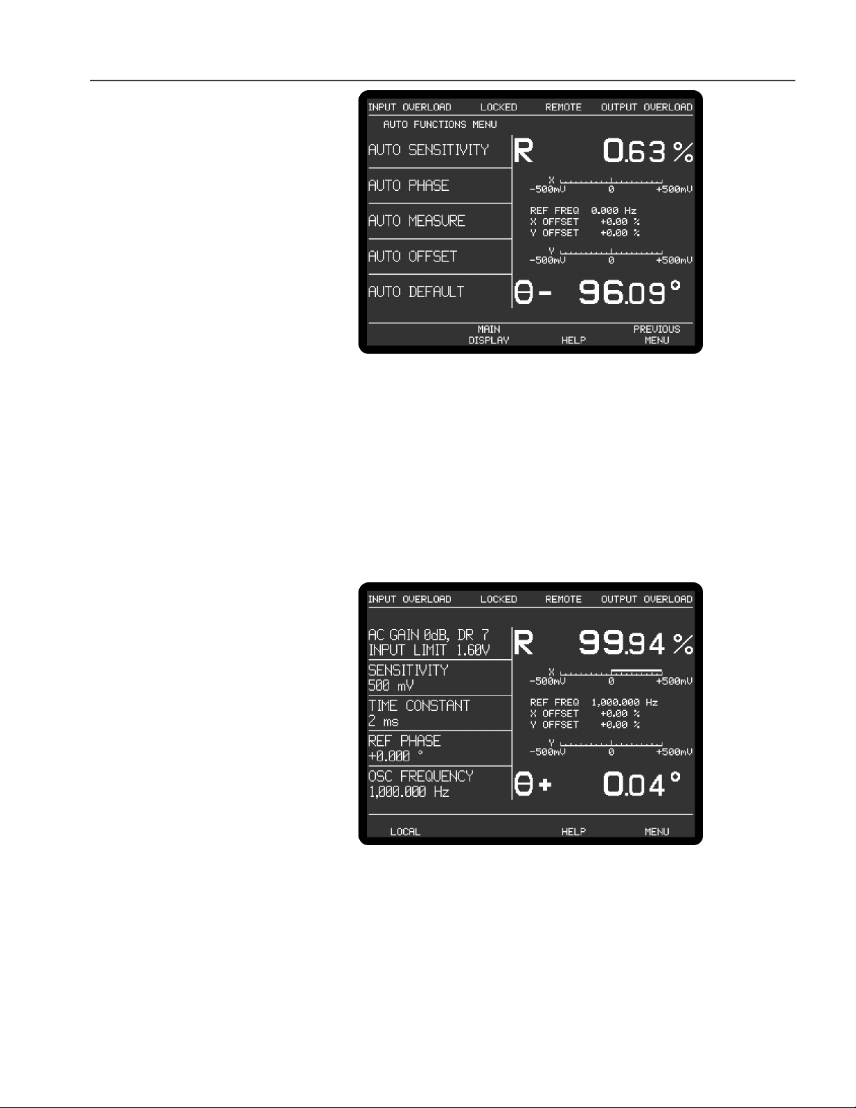
Chapter 2, INSTALLATION & INITIAL CHECKS
Figure 2-4, Auto Functions Menu
7) Press one of the keys adjacent to the Auto Default menu item. This will set all of
the instrument's controls and the display to a defined state. The display will
revert to the Main Display, as shown below in figure 2-5, with the right-hand
side showing the vector magnitude, R, and the phase angle, θ, of the measured
signal in digital form, with two bar-graphs showing the X channel output and Y
channel output expressed in millivolts. The left-hand side shows five instrument
controls, these being the AC Gain in decibels, full-scale sensitivity, output time
constant, reference phase and internal oscillator frequency. The resulting
dynamic reserve (DR), in decibels, is also shown.
Figure 2-5, Main Display
8) Connect a BNC cable between the OSC OUT and A input connectors on the
front panel.
2-5
Page 18

Chapter 2, INSTALLATION & INITIAL CHECKS
9) The right-hand side of the display should now indicate R, the vector magnitude,
close to 100% of full-scale (i.e. the sinusoidal oscillator output, which was set to
1 kHz and a signal level of 0.5 V rms by the Auto-Default function, is being
measured with a full-scale sensitivity of 500 mV rms) and θ, the phase angle, of
near zero degrees, if a short cable is used.
This completes the initial checks. Even though the procedure leaves many functions
untested, if the indicated results were obtained then the user can be reasonably sure
that the unit incurred no hidden damage in shipment and is in good working order.
2.3 Line Frequency Filter Adjustment
2.3.01 Introduction
The model 7280 incorporates a line-frequency rejection filter which is normally
supplied set to 60 Hz. If the power line frequency of the country in which the
instrument is to be used is also 60 Hz then the setting does not need to be changed. If,
however, the unit is to be used in an area with a 50 Hz power line frequency the
setting should be changed using the following procedure.
2.3.02 Procedure
1) Turn the model 7280’s power switch to the I (on) position.
2) The instrument's front panel display will now briefly display the following:-
Figure 2-6, Opening Display
2-6
3) Wait until the opening display has changed to the Main Display and then press
the key under the bottom right hand corner of the display identified by the legend
MENU on the display once. This enters the first of the two main menus, Main
Menu 1, shown below in figure 2-7.
Page 19

Chapter 2, INSTALLATION & INITIAL CHECKS
Figure 2-7, Main Menu 1
4) Press one of the keys adjacent to the Configuration menu item to enter the
Configuration menu, shown below in figure 2-8.
Figure 2-8, Configuration Menu
5) The present line frequency setting is shown in reversed text under the
LINE FREQUENCY label and is either 50 or 60 Hz. In figure 2-8, the filter is set
to 60 Hz. If this setting does not match the prevailing line frequency, then press a
key adjacent to this item once to change it.
6) Press the key marked MAIN DISPLAY once to return to the Main Display.
This completes the procedure for adjusting the line frequency filter.
2-7
Page 20

Chapter 2, INSTALLATION & INITIAL CHECKS
2-8
Page 21

Technical Description
3.1 Introduction
The model 7280 lock-in amplifier is a sophisticated instrument with many
capabilities beyond those found in other lock-in amplifiers. This chapter discusses the
various operating modes provided and then describes the design of the instrument by
considering it as a series of functional blocks. In addition to describing how each
block operates, the sections also include information on the effect of the various
controls.
3.2 Operating Modes
3.2.01 Introduction
The model 7280 incorporates a number of different operating modes which are
referred to in the following technical description, so in order to help the reader's
understanding they are defined here.
3.2.02 Single Reference / Dual Reference
Chapter 3
Conventionally, a lock-in amplifier makes measurements such as signal magnitude,
phase, etc. on the applied signal at a single reference frequency. In the model 7280
this is referred to as the single reference mode.
The dual reference mode incorporated in the model 7280 allows the instrument to
make simultaneous measurements at two different reference frequencies, an ability
that previously required two lock-in amplifiers. This flexibility incurs a few
restrictions, such as the requirement that one of the reference signals be external and
the other be derived from the internal oscillator, the limitation of the maximum
operating frequency to 20 kHz (unless the unit is equipped with the -/99 or -/98
extended frequency options) and the requirement that both signals be passed through
the same input signal channel. This last restriction implies either that both signals are
derived from the same detector (for example two chopped light beams falling onto a
single photodiode) or that they can be summed prior to measurement, either
externally or by using the differential input mode of the instrument. Nevertheless, the
mode will prove invaluable in many experiments.
3.2.03 Single Harmonic / Dual Harmonic
Normally, a lock-in amplifier measures the applied signal at the reference frequency.
However, in some applications such as Auger Spectroscopy and amplifier
characterization, it is useful to be able to make measurements at some multiple n, or
harmonic, of the reference frequency, f. The model 7280 allows this multiple to be set
to any value between 2 (i.e. the second harmonic) and 32, as well as unity, which is
the normal mode. The only restriction is that the product n × f cannot exceed 2 MHz.
Dual harmonic mode allows the simultaneous measurement of two different
harmonics of the input signal. As with dual reference mode, there are a few
restrictions, such as a maximum value of n × f of 20 kHz (800 kHz with the option /99 or 2 MHz with the option -/98).
3-1
Page 22

Chapter 3, TECHNICAL DESCRIPTION
3.2.04 Internal / External Reference Mode
In the internal reference mode, the instrument's reference frequency is derived from
its internal oscillator and the oscillator signal is used to drive the experiment.
In the external reference mode, the experiment includes some device, for example an
optical chopper, which generates a reference frequency that is applied to one of the
lock-in amplifier's external reference inputs. The instrument's reference channel
"locks" to this signal and uses it to measure the applied input signal.
3.2.05 Virtual Reference Mode
If the instrument is operated in internal reference mode, measuring a signal which is
phase-locked to the internal oscillator, with the reference phase correctly adjusted,
then it will generate a stable non-zero X channel output and a zero Y channel output.
If, however, the signal is derived from a separate oscillator, then the X channel and
Y channel outputs will show variations at a frequency equal to the difference between
the signal and internal oscillator frequencies. If the latter is now set to be equal to the
former then in principle the variation in the outputs will cease, but in practice this
will not happen because of slow changes in the relative phase of the two oscillators.
In the virtual reference mode, believed to be unique to SIGNAL RECOVERY lockin amplifiers, the Y channel output is used to make continuous adjustments to the
internal oscillator frequency and phase to achieve phase-lock with the applied signal,
such that the X channel output is maximized and the Y channel output zeroed.
If the instrument is correctly adjusted, particularly ensuring that the full-scale
sensitivity control is maintained at a suitable setting in relation to changes in the
signal level, then the virtual reference mode is capable of making signal recovery
measurements which are not possible with most other lock-in amplifiers.
3.3 Principles of Operation
3.3.01 Block Diagram
The model 7280 uses digital signal processing (DSP) techniques implemented in
field-programmable gate arrays (FPGA), a microprocessor and very low-noise analog
circuitry to achieve its specifications. A block diagram of the instrument is shown in
figure 3-1. The sections that follow describe how each functional block operates and
the effect it has on the instrument's performance.
3-2
Page 23

Chapter 3, TECHNICAL DESCRIPTION
Figure 3-1, Model 7280 - Block Diagram
3.3.02 Signal Channel Inputs
The signal input amplifier can be set for either single-ended or differential voltage
mode operation, or single-ended current mode operation. In voltage mode a choice of
AC or DC coupling is available using an FET input device. In current mode a choice
of three conversion gains is available to give optimum matching to the applied signal.
In both modes the input connector shells may be either floated via a 1 kΩ resistor or
grounded to the instrument's chassis ground. These various features are discussed in
the following paragraphs.
Input Connector Selection, A / -B / A - B
When set to the A mode, the lock-in amplifier measures the voltage between the
center and the shell of the A input BNC connector, whereas when set to the A-B
mode it measures the difference in voltage between the center pins of the A and B/I
input BNC connectors.
The latter, differential, mode is often used to eliminate ground loops, although it is
worth noting that at very low signal levels it may be possible to make a substantial
reduction in unwanted offsets by using this mode with a short-circuit terminator on
the B/I connector, rather than by simply using the A input mode.
The specification defined as the Common Mode Rejection Ratio, C.M.R.R., describes
how well the instrument rejects common mode signals applied to the A and B/I
inputs when operating in differential input mode. It is usually given in decibels.
Hence a specification of > 100 dB implies that a common mode signal (i.e. a signal
simultaneously applied to both A and B/I inputs) of 1 V will give rise to less than
10 µV of signal out of the input amplifier.
The input can also be set to the -B mode, in which case the lock-in amplifier
measures the voltage between the center and the shell of the B/I input connector. This
extra mode effectively allows the input to be multiplexed between two different
3-3
Page 24

Chapter 3, TECHNICAL DESCRIPTION
single-ended signals, subject to the limitation that the user must allow for the signal
inversion (equivalent to a 180° phase-shift) which it introduces when reading the
outputs.
Input Connector Shell, Ground / Float
The input connector shells may be connected either directly to the instrument's
chassis ground or floated via a 1 kΩ resistor. When in the float mode, the presence of
this resistor substantially reduces the problems which often occur in low-level lock-in
amplifier measurements due to ground loops.
Input Coupling Mode, Fast/Slow
When the input coupling mode is set to Slow, the signal channel gain is essentially
flat down to 0.5 Hz, but recovery from input overload conditions may take a long
time. Conversely, when the coupling mode is set to Fast, recovery from overload is
much faster, but there will be a noticeable roll-off in magnitude response and
significant phase shifts at frequencies below typically 20 Hz.
Input Signal Selection, V / I
Although the voltage mode input is most commonly used, a current-to-voltage
converter may be switched into use to provide current mode input capability, in
which case the signal is connected to the B/I connector. High impedance sources
(> 100 kΩ) are inherently current sources and need to be measured with a low
impedance current mode input. Even when dealing with a voltage source in series
with a high impedance, the use of the current mode input may provide advantages in
terms of improved bandwidth and immunity from the effects of cable capacitance.
The converter may be set to low-noise, normal or wide bandwidth conversion
settings, but it should be noted that if the best possible performance is required a
separate current preamplifier, such as the SIGNAL RECOVERY models 181 or
5182, should be considered.
3.3.03 Line Frequency Rejection Filter
Following the signal input amplifier there is an option to pass the signal through a
line frequency rejection filter, which is designed to give greater than 40 dB of
attenuation at the power line frequencies of 50 Hz or 60 Hz and their second
harmonics at 100 Hz and 120 Hz.
The filter uses two cascaded rejection stages with "notch" characteristics, allowing it
to be set to reject signals at frequencies equal to either of, or both of, the fundamental
and second harmonic of the line frequency.
Instruments are normally supplied with the line frequency filter set to 60 Hz with the
filter turned off. If the prevailing line frequency is 50 Hz then the filter frequency
should be set to this value using the control on the Configuration menu (see section
2.3).
3.3.04 AC Gain and Dynamic Reserve
3-4
The signal channel contains a number of analog filters and amplifiers whose overall
gain is defined by the AC Gain parameter, which is specified in terms of decibels
(dB). For each value of AC Gain there is a corresponding value of the INPUT LIMIT
Page 25

Chapter 3, TECHNICAL DESCRIPTION
parameter, which is the maximum instantaneous (peak) voltage or current that can be
applied to the input without causing input overload, as shown in table 3-1 below.
AC Gain (dB) INPUT LIMIT (mV)
0 1600
6 800
14 320
20 160
26 80
34 32
40 16
46 8
54 3.2
60 1.6
66 0.8
Table 3-1, Input Limit vs. AC Gain
It is a basic property of the digital signal processing (DSP) lock-in amplifier that the
best demodulator performance is obtained by presenting as large a signal as possible
to the main analog-to-digital converter (ADC). Therefore, in principle, the AC Gain
value should be made as large as possible without causing the signal channel
amplifier or converter to overload. This constraint is not too critical however and the
use of a value one or two steps below the optimum value makes little difference. Note
that as the AC Gain value is changed, the demodulator gain (described later in section
3.3.12) is also adjusted in order to maintain the selected full-scale sensitivity.
The full-scale sensitivity is set by a combination of AC Gain and demodulator gain.
Since the demodulator gain is entirely digital, changes in full-scale sensitivity which
do not change the AC Gain do not cause any of the errors which might arise from a
change in the AC Gain.
The user is prevented from setting an illegal AC Gain value, i.e. one that would result
in overload on a full-scale input signal. Similarly, if the user selects a full-scale
sensitivity which causes the present AC Gain value to be illegal, the AC Gain will
change to the nearest legal value.
In practice, this system is very easy to operate. However, the user may prefer to make
use of the AUTOMATIC AC Gain feature which gives very good results in most
cases. When this is active the AC Gain is automatically controlled by the instrument,
which determines the optimum setting based on the full-scale sensitivity currently
being used.
At any given setting, the ratio
0.7DR ×=
LimitInput
ySensitivit Scale-Full
represents the factor by which the largest acceptable sinusoidal interference input
exceeds the full-scale sensitivity and is called the Dynamic Reserve of the lock-in
amplifier at that setting. (The factor 0.7 is a peak-to-rms conversion). The dynamic
3-5
Page 26

Chapter 3, TECHNICAL DESCRIPTION
reserve is often expressed in decibels, for which
Applying this formula to the model 7280 at the maximum value of INPUT LIMIT
(1.6 V) and the smallest available value of FULL-SCALE SENSITIVITY (10 nV),
gives a maximum available dynamic reserve of about 1 × 10
this magnitude are available from any DSP lock-in amplifier but are based only on
arithmetical identities and do not give any indication of how the instrument actually
performs. In fact, all current DSP lock-in amplifiers become too noisy and inaccurate
for most purposes at reserves of greater than about 100 dB.
For the benefit of users who prefer to have the AC Gain value expressed in decibels,
the model 7280 displays the current value of Dynamic Reserve (DR) in this form, on
the input full-scale sensitivity control, for values up to 100 dB. Above 100 dB the
legend changes to “DR>100”.
3.3.05 Anti-Aliasing Filter
Prior to the main analog-to-digital converter (ADC) the signal passes through an antialiasing filter to remove unwanted frequencies which would cause a spurious output
from the ADC as a result of the sampling process.
))ratio a log(DR(as20dB)DR(in ×=
8
or 160 dB. Figures of
Consider the situation when the lock-in amplifier is measuring a sinusoidal signal of
frequency f
Hz. In order to ensure correct operation of the instrument the output values
f
sampling
representing the f
Hz, which is sampled by the main ADC at a sampling frequency
signal
frequency must be uniquely generated by the signal to be
signal
measured, and not by any other process.
However, if the input to the ADC has, in addition, an unwanted sinusoidal signal
with frequency f
Hz, where f1 is greater than half the sampling frequency, then this
1
will appear in the output as a sampled-data sinusoid with frequency less than half the
sampling frequency, f
= |f1 - nf
alias
indistinguishable from the output generated when a genuine signal at frequency f
|, where n is an integer. This alias signal is
sampling
alias
is sampled. Hence if the frequency of the unwanted signal were such that the alias
signal frequency produced from it was close to, or equal to, that of the wanted signal
then it is clear that a spurious output would result.
For example, if the sampling frequency were 7.5 MHz then half the sampling
frequency would be 3.75 MHz. Assume for a moment that the instrument could
operate at reference frequencies up to 3.75 MHz and let it be measuring a signal of
40 kHz accompanied by an interfering signal of 3.7 MHz. The output of the ADC
would therefore include a sampled-data sinusoid of 40 kHz (the required signal) and,
applying the above formula, an alias signal of 0.05 MHz, or 50 kHz (i.e. |3.75 MHz -
3.7 MHz|). If the signal frequency were now increased towards 50 kHz then the
output of the lock-in amplifier would increasingly be affected by the presence of the
alias signal and the accuracy of the measurement would deteriorate.
3-6
To overcome this problem the signal is fed through the anti-aliasing filter which
restricts the signal bandwidth to an upper frequency of 2.0 MHz The filter is a
conventional elliptic-type, low-pass, stage, giving the lowest possible noise
Page 27

Chapter 3, TECHNICAL DESCRIPTION
bandwidth.
It should be noted that the dynamic range of a lock-in amplifier is normally so high
that practical anti-alias filters are not capable of completely removing the effect of a
full-scale alias. For instance, even if the filter gives 100 dB attenuation, an alias at the
input limit and at the reference frequency will give a one percent output error when
the dynamic reserve is set to 60 dB, or a ten percent error when the dynamic reserve
is set to 80 dB.
In a typical low-level signal recovery situation, many unwanted inputs need to be
dealt with and it is normal practice to make small adjustments to the reference
frequency until a clear point on the frequency spectrum is reached. In this context an
unwanted alias is treated as just another interfering signal and its frequency is
avoided when setting the reference frequency.
A buffered version of the analog signal just prior to the main ADC is available at the
signal monitor (SIG MON) connector on the rear panel; it may be viewed on an
oscilloscope to monitor the effect of the line frequency rejection and anti-aliasing
filters and signal-channel amplifiers.
3.3.06 Main Analog-to-Digital Converter
Following the anti-alias filter the signal passes to the main analog-to-digital converter
running at a sampling rate of 7.5 MHz. The output from the converter feeds the
demodulator circuitry, which uses DSP techniques to implement the digital
multipliers and the first stage of the output low-pass filtering for each of the X and Y
channels.
The ADC output also passes to the output processor to allow the power spectral
density of the input signal to be calculated using a discrete Fourier transform, which
in many ways is similar to a fast Fourier transform (FFT). The results of this
calculation are shown on the Spectral Display menu.
However, before discussing the demodulators and the output stages of the lock-in
amplifier, the reference channel which provides the other input to the demodulators,
will be described.
3.3.07 Reference Channel
The reference channel in the instrument is responsible for implementing the reference
trigger/phase-locked loop, digital phase-shifter and internal oscillator look-up table
functional blocks on the block diagram (see figure 3-1). The processor generates a
series of phase values, output at a rate of one every 133 ns, which are used to drive
the reference channel inputs of the demodulators.
In dual reference mode operation, an externally derived reference frequency is
connected to the external reference input and a second reference is derived from the
internal oscillator. The reference circuit generates new phase values for each
individual channel and sends these to the demodulators. Further discussion of dual
reference mode occurs in section 3.3.12.
In single harmonic mode, the reference circuit generates the phase values of a
3-7
Page 28

Chapter 3, TECHNICAL DESCRIPTION
waveform at the selected harmonic of the reference frequency. Dual harmonic mode
operates in a similar way to dual reference mode, but in this case the reference circuit
generates phase values for both of the selected harmonics of the reference frequency.
Dual harmonic mode may therefore be used with either internal or external
references.
External Reference Mode
In external reference mode the reference source may be applied to either a general
purpose input, designed to accept virtually any periodic waveform with a 50:50
mark-space ratio and of suitable amplitude, or to a TTL-logic level input. Following
the trigger buffering circuitry the reference signal is passed to a digital phase-locked
loop (PLL) implemented in the reference circuit. This measures the period of the
applied reference waveform and from this generates the phase values.
Internal Reference Mode
With internal reference operation the reference circuit is free-running at the selected
reference frequency and is not dependent on a phase-locked loop (PLL), as is the case
in most other lock-in amplifiers. Consequently, the phase noise is extremely low, and
because no time is required for a PLL to acquire lock, reference acquisition is
immediate.
Both the signal channel and the reference channel contain calibration parameters
which are dependent on the reference frequency. These include corrections to the
anti-alias filter and to the analog circuits in the reference channel. In external
reference operation the processor uses a reference frequency meter to monitor the
reference frequency and updates these parameters when a change of about 2 percent
has been detected.
A TTL logic signal at the present reference frequency is provided at the REF MON
connector on the rear panel.
3.3.08 Phase-Shifter
The reference circuit also implements a digital reference phase-shifter, allowing the
phase values being sent to the demodulator DSP to be adjusted to the required value.
If the reference input is a sinusoid applied to the REF IN socket, the reference phase
is defined as the phase of the X demodulation function with respect to the reference
input.
This means that when the reference phase is zero and the signal input to the
demodulator is a full-scale sinusoid in phase with the reference input sinusoid, the X
channel output of the demodulator is a full-scale positive value and the Y channel
output is zero.
3-8
The circuits connected to the REF IN socket detect a positive-going crossing of the
mean value of the applied reference voltage. Therefore when the reference input is
not sinusoidal, its effective phase is the phase of a sinusoid with a positive-going zero
crossing at the same point in time, and accordingly the reference phase is defined
with respect to this waveform. Similarly, the effective phase of a reference input to
the TTL REF IN socket is that of a sinusoid with a positive-going zero crossing at
the same point in time.
Page 29

Chapter 3, TECHNICAL DESCRIPTION
In basic lock-in amplifier applications the purpose of the experiment is to measure
the amplitude of a signal which is of fixed frequency and whose phase with respect to
the reference input does not vary. This is the scalar measurement, often implemented
with a chopped optical beam. Many other lock-in amplifier applications are of the
signed scalar type, in which the purpose of the experiment is to measure the
amplitude and sign of a signal which is of fixed frequency and whose phase with
respect to the reference input does not vary apart from reversals of phase
corresponding to changes in the sign of the signal. A well-known example of this
situation is the case of a resistive bridge, one arm of which contains the sample to be
measured. Other examples occur in derivative spectroscopy, where a small
modulation is applied to the angle of the grating (in optical spectroscopy) or to the
applied magnetic field (in magnetic resonance spectroscopy). Double beam
spectroscopy is a further common example.
In this signed scalar measurement the phase-shifter must be set, after removal of any
zero errors, to maximize the X channel or the Y channel output of the demodulator.
This is the only method that will give correct operation as the output signal passes
through zero, and is also the best method to be used in an unsigned scalar
measurement where any significant amount of noise is present.
3.3.09 Internal Oscillator - General
The model 7280, in common with many other lock-in amplifiers, incorporates an
internal oscillator which may be used to drive an experiment. However, unlike most
other instruments, the oscillator in the model 7280 is digitally synthesized with the
result that the output frequency is extremely accurate and stable. The oscillator
operates over the same frequency range as the lock-in amplifier, that is 500 mHz to
2.0 MHz, and is implemented using a dedicated direct digital synthesis circuit.
3.3.10 Internal Oscillator - Update Rate
The direct digital synthesis (DDS) technique generates a waveform at the DAC
output which is not a pure sinusoid, but rather a stepped approximation to one. This
is then filtered by the buffer stage, which follows the DAC, to reduce the harmonic
distortion to an acceptable level. The update rate is 22.5 MHz.
3.3.11 Internal Oscillator - Frequency & Amplitude Sweeps
The internal oscillator output may be swept in both frequency and amplitude. In both
cases the sweeps take the form of a series of steps between starting and finishing
values. Frequency sweeps may use equal increment step sizes, giving a linear change
of frequency with time as the sweep proceeds, or may use step sizes proportional to
the present frequency, which produces a logarithmic sweep. The amplitude sweep
function offers only linear sweeps.
A special form of the frequency sweep function is used to acquire lock when the
instrument is operating in the virtual reference mode. When this "seek" sweep is
activated, the oscillator starts at a user-specified frequency, which should be just
below that of the applied signal, and increments until the calculated magnitude output
is greater than 50%. At this point the sweep then stops and the virtual reference mode
achieves lock, by continuously adjusting the internal oscillator frequency to maintain
the Y channel output at zero.
3-9
Page 30

Chapter 3, TECHNICAL DESCRIPTION
It is important to note that this type of phase-locked loop, unlike a conventional edgetriggered type using a clean reference, does not automatically re-acquire lock after it
has been lost. Lock can be lost as a result of a signal channel transient or a phase
reversal of the signal, in which case it may be necessary to repeat the lock acquisition
procedure. However, if the measurement system is set up with sufficient precautions,
particularly ensuring that the full-scale sensitivity is maintained at a suitable setting
in relation to the signal level, then the virtual reference mode is capable of making
signal recovery measurements which are not possible with other lock-in amplifiers.
When virtual reference mode is in use, the signal at the OSC OUT connector is a
sinusoid which is phase-locked to the signal. Naturally, this cannot be used as a
source for the measurement.
3.3.12 Demodulators
The essential operation of the demodulators is to multiply the digitized output of the
signal channel by data sequences, called the X and Y demodulation functions, and to
operate on the results with digital low-pass filters (the output filters). The
demodulation functions, which are derived by use of a look-up table from the phase
values supplied by the reference channel DSP, are sinusoids with a frequency equal
to an integer multiple, n × f, of the reference frequency f. The Y demodulation
function is the X demodulation function delayed by a quarter of a period. The integer
n is called the reference harmonic number and in normal lock-in amplifier operation
is set to unity. Throughout this chapter, the reference harmonic number is assumed to
be unity unless otherwise stated.
The outputs from the X channel and Y channel multipliers feed the first stage of the
X channel and Y channel output filters, implemented as Finite Impulse Response
(FIR) stages with selectable 6 or 12 dB/octave roll-off. The filtered X channel signal
drives a 16-bit DAC that, for short time-constant settings, generates the signal at the
instrument's CH 1 analog output connector. Both signals are combined by a fast
magnitude algorithm and a switch then allows either the filtered Y channel signal or
the magnitude signal, again when using short time-constant settings, to be passed to a
second 16-bit DAC to give the signal at the instrument's CH 2 analog output. The
significance of the magnitude output is discussed later in section 3.3.15.
In addition the X and Y channel signals are fed to further low-pass filters before
subsequent processing by the instrument’s host microprocessor.
The demodulator output is digitally scaled to provide the demodulator gain control.
As discussed earlier in section 3.3.04 this gain is adjusted as the AC Gain is adjusted
to maintain a given full-scale sensitivity.
In dual reference and dual harmonic modes, the demodulators generate two sets of
outputs, one for each of the two references or harmonics, and includes two sets (four
channels) of initial output filtering. These outputs are passed to the host processor for
further processing and, when the time constant is less than 1 ms, the X
and X
1
2
outputs are also converted by fast DACs to analog signals that appear at the CH 1
and CH 2 analog output connectors.
3-10
Page 31

Chapter 3, TECHNICAL DESCRIPTION
3.3.13 Output Processor - Output Filters
Although shown on the block diagram as a separate entity, the output processor is in
fact part of the instrument's main microprocessor. It provides more digital filtering of
the X channel and Y channel signals if this is needed in addition to that already
performed by the demodulators. As with most lock-in amplifiers, the output filter
configuration in the model 7280 is controlled by the slope control. This may seem
somewhat strange, and a few words of explanation may be helpful.
In traditional audio terminology, a first-order low-pass filter is described as having a
slope of 6 dB per octave because in the high frequency limit its gain is inversely
proportional to frequency (6 dB is approximately a factor of 2 in amplitude and an
octave is a factor of 2 in frequency); similarly a second-order low-pass filter is
described as having a slope of 12 dB per octave. These terms have become part of the
accepted terminology relating to lock-in amplifier output filters and are used in the
model 7280 to apply to the envelope of the frequency response function of the digital
finite impulse response (FIR) output filters. Accordingly the front-panel control
which selects the configuration of the output filters is labeled SLOPE and the options
are labeled 6, 12, 18, 24 dB/octave.
The 6 dB/octave filters are not satisfactory for most purposes because they do not
give good rejection of non-random interfering signals which can cause aliasing
problems as a result of the sampling process in the main ADC. However, the
6 dB/octave filter finds use where the lock-in amplifier is incorporated in a feedback
control loop, and in some situations where the form of the time-domain response is
critical. The user is recommended to use 12 dB/octave unless there is some definite
reason for not doing so.
Note that at short time constant settings the filter slope options are limited to 6 or
12 dB/octave.
The output time constant can be varied between 1 µs and 100 ks. When set to a value
between 1 µs and 1 ms or 4 ms, X and Y or X and Magnitude outputs are available at
the CH 1 and CH 2 outputs. At longer time constant settings, all outputs are valid
and available at the CH 1 and CH 2 outputs and as the internal digital values
reported to a remote computer or stored to the internal curve buffer. The large digital
displays and bar-graph indicators on the front panel have an effective minimum time
constant limit imposed by their update rates, which are 512 ms and 64 ms
respectively. As noted in section 3.3.12 above, in dual reference and dual harmonic
modes the analog outputs at time constants shorter than 1 ms are limited to X
.
X
2
and
1
The filters are of the finite impulse response type with the averaging time of each
section being equal to double the nominal time constant. These filters offer a
substantial advantage in response time compared with analog filters or digital infinite
impulse response (IIR) filters.
When the reference frequency is below 10 Hz the synchronous filter option is
available. This means that the actual time constant of the filter is not generally the
selected value T, but a value which is equal to an integer number of reference cycles.
If T is greater than 1 reference cycle, then the time constant is between T/2 and T.
3-11
Page 32

Chapter 3, TECHNICAL DESCRIPTION
Where random noise is relatively small, synchronous filter operation gives a major
advantage in low-frequency measurements by enabling the system to give a constant
output even when the output time constant is equal to only 1 reference cycle.
3.3.14 Output Processor - Output Offset and Expand
Following the output filter, an output offset facility enables ±300% full-scale offset
to be applied to the X, Y or both displays and to the analog outputs.
The output expand facility allows a ×10 expansion, performed by simple internal
digital multiplication, to be applied to the X, Y, both or neither outputs, and hence to
the bar-graph displays and the CH 1 and CH 2 analog outputs, if these are set to
output X or Y values.
3.3.15 Output Processor - Vector Magnitude and Phase
The processor also implements the magnitude and signal phase calculation which is
useful in many situations. If the input signal V
constant amplitude, and the output filters are set to a sufficiently long time constant,
the demodulator outputs are constant levels V
dependent only on the amplitude of the required signal V
on the phase of V
output processor in the lock-in amplifier and made available as the magnitude output.
The phase angle between V
phase: this is equal to the angle of the complex quantity (V
square root of -1) and is also computed by the processor by means of a fast arc tan
algorithm.
(t) is a reference frequency sinusoid of
s
and Vy. The function √(V
x
(t) (i.e. it is not dependent
s
(t) with respect to the reference input) and is computed by the
s
(t) and the X demodulation function is called the signal
s
+ jVy) (where j is the
x
2
x
+ V
2
) is
y
The magnitude and signal phase outputs are used in cases where phase is to be
measured, or alternatively where the magnitude is to be measured under conditions of
uncertain or varying phase.
One case of varying phase is that in which the reference input is not derived from the
same source as that which generates the signal, and is therefore not at exactly the
same frequency. In this case, if the input signal is a sinusoid of constant amplitude,
the X channel and Y channel demodulator outputs show slow sinusoidal variations at
the difference frequency, and the magnitude output remains steady.
However, the magnitude output has disadvantages where significant noise is present
at the outputs of the demodulator. When the required signal outputs (i.e. the mean
values of the demodulator outputs) are less than the noise, the outputs take both
positive and negative values but the magnitude algorithm gives only positive values:
this effect, sometimes called noise rectification, gives rise to a zero error which in the
case of a Gaussian process has a mean value equal to 0.798 times the combined rootmean-square (rms) value of the X and Y demodulator noise. Note that unlike other
forms of zero error this is not a constant quantity which can be subtracted from all
readings, because when the square root of the sum of the squares of the required
outputs becomes greater than the total rms noise the error due to this mechanism
disappears.
A second type of signal-dependent error in the mean of the magnitude output occurs
3-12
Page 33

Chapter 3, TECHNICAL DESCRIPTION
as a result of the inherent non-linearity of the magnitude formula: this error is always
positive and its value, expressed as a fraction of the signal level, is half the ratio of
the mean-square value of the noise to the square of the signal.
These considerations lead to the conclusion that when the magnitude output is being
used, the time constants of the demodulator should be set to give the required signalto-noise ratio at the X channel and Y channel demodulator outputs; improving the
signal-to-noise ratio by averaging the magnitude output itself is not to be
recommended.
For analogous reasons, the magnitude function also shows signal-dependent errors
when zero offsets are present in the demodulator. For this reason, it is essential to
reduce zero offsets to an insignificant level (usually by the use of the Auto-Offset
function) when the magnitude output is to be used.
Note that the majority of signal recovery applications are scalar measurements, where
the phase between the required signal and the reference voltage is constant apart from
possible phase reversals corresponding to changes in the sign of the quantity being
measured. In this situation the lock-in amplifier is used in the normal X-Y mode, with
the phase-shifter adjusted to maximize the X output and to bring the mean Y output
to zero. (Refer to section 3.3.21 for further information on the correct use of the
Auto-Phase function for this purpose.)
3.3.16 Output Processor - Noise Measurements
The noise measurement facility uses the output processor to perform a noise
computation on the X output of the demodulator. A noise buffer continuously
calculates the mean level of X, representing the measured output signal, by summing
the last n samples of the X output and dividing by n. The processor then calculates
the modulus of the difference between each X-output value and the mean value and
uses this figure to derive the noise. The displayed noise value is correct for input
noise where the amplitude distribution of the waveform is Gaussian, which is
normally the case. The indicated value (in V/√Hz or A/√Hz) is the square root of the
mean spectral density over the equivalent noise bandwidth defined by the setting of
the output filter time constant and slope.
When used for noise measurements, the available range of output time constants is
restricted to 500 µs to 10 ms inclusive, and the slope to 6 or 12 dB/octave. The
corresponding actual bandwidth for the present time constant and slope settings can
be found from the table 3-2 below, or by using the ENBW. command. In addition,
the Synchronous Time Constant control is turned off.
Time Equivalent Noise Bandwidth at Output Filter Slope (Hz)
Constant 6 dB/octave 12 dB/octave
500 µs
1 ms
2 ms
4 ms
5 ms
10 ms
335 276
209 158
115 82
60 42
48 33
24 17
Table 3-2, ENBW vs. Time Constant and Slope
3-13
Page 34

Chapter 3, TECHNICAL DESCRIPTION
The noise buffer length n can be set to 1, 1000, 2000, 3000 or 4000. Since new input
values to the buffer are supplied at a 1 kHz rate, these correspond to averaging times
of zero, 1 second, 2 seconds, 3 seconds and 4 seconds respectively, and so the control
on the Configuration Menu that adjusts this buffer length is labeled Noise Buffer
Length and can be set to Off, 1 s, 2 s, 3 s or 4 s. Setting a shorter time means that the
system responds more quickly to changes in the mean X-output level, but the noise
reading itself exhibits more fluctuation. Conversely, the fluctuation can be reduced
by setting a longer time, but at the expense of increased settling time following
changes in the mean X-output level.
If a noise output (N calibrated in volts or amps per root hertz, or as a percentage of
full scale) is selected as one of the outputs on the Main Display or for conversion to
an analog signal for output to the CH1/CH2 outputs, and the time constant is not
within the permitted range then a warning message is displayed on the screen.
Similarly, if a noise output value is read via the computer interfaces while the time
constant or slope are outside the permitted range, or if the synchronous time constant
control is enabled, then the response will be -1. Since noise readings can only be zero
or positive, this negative number clearly indicates that the reading is invalid and
should be ignored.
In order to make noise measurements easier, the instrument includes a Noise
Measurement Mode, activated by a control on the Configuration menu or by a
computer command. When this is turned on, the Main Display outputs are set to the
four types most commonly required, and the filter time constant, slope and
synchronous time constant setting are forced to values within the permitted ranges.
When turned off, these restrictions are removed.
When making noise measurements the user is strongly advised to use an oscilloscope
to monitor the signal at the SIG MON output on the rear panel as this is the best way
of ensuring that a random process is being measured rather than line pick-up or other
non-random signals.
Any two of the outputs, including X channel and Y channel signals, vector
magnitude, and phase angle, and even noise may be represented in analog form by
being routed via two further 16-bit DACs to the unit's CH 1 and CH 2 output
connectors.
3.3.17 Auxiliary Analog Inputs and Outputs (ADCs and
DACs)
The model 7280 incorporates four auxiliary ADC inputs of conventional sampled
design offering a resolution of 1 mV in ±10.000 V. These converters may be used at
slow sample rates for digitizing slowly changing or DC signals which are associated
with an experiment, such as those generated by temperature and pressure transducers,
so that they can be incorporated into ratio calculations or transferred to a controlling
computer. They may also be used in conjunction with the instrument's curve buffer to
form a transient recorder operating at sample rates of up to 40 kHz.
Two auxiliary DAC outputs are also provided which offer the same resolution as the
ADCs, namely 1 mV in ±10.000 V.
3-14
Page 35

Chapter 3, TECHNICAL DESCRIPTION
3.3.18 Main Microprocessor - Spectral Display
In some cases it can be useful to determine the spectral power distribution of the
input signal. The model 7280 can do this, since when the Spectral Display menu is
selected, the output processor performs a discrete Fourier transform on the digitized
input signal and displays the resulting spectrum.
3.3.19 Main Microprocessor - User Settings
The non-volatile memory associated with the main microprocessor is used to store up
to eight complete instrument settings, which may be recalled or changed as required.
This makes it much easier for an instrument to be quickly configured for different
experiments.
3.3.20 Main Microprocessor - General
All functions of the instrument are under the control of a microprocessor which in
addition drives the front-panel display, processes front-panel key operations and
supports the RS232 and GPIB (IEEE-488) computer interfaces. This processor also
drives the instrument's 8-bit digital (TTL) programmable input/output port, which
may be used for controlling auxiliary apparatus or reading the status of external logic
lines.
The microprocessor has access to a 32,768 point memory which can be used for
storage of selected instrument outputs as curves, prior to their transfer to a computer
via the computer interfaces. In addition to using this function for the normal outputs,
such as the X channel and Y channel output signals, it may also be used with two of
the auxiliary ADC inputs to allow the instrument to operate as a transient recorder.
The internal oscillator frequency and amplitude sweep functions are also controlled
by the microprocessor.
A particularly useful feature of the design is that only part of the controlling firmware
program code, which the microprocessor runs, is permanently resident in the
instrument. The remainder is held in a flash EEPROM and can be updated via the
RS232 computer interface. It is therefore possible to change the functionality of the
instrument, perhaps to include a new feature or update the computer command set,
simply by connecting it to a computer and running an update program.
3.3.21 Main Microprocessor - Auto Functions
The microprocessor also controls the instrument's auto functions, which are control
operations executed by means of a single command or two key-presses. These
functions allow easier, faster operation in most applications, although direct manual
operation or special purpose control programs may give better results in certain
circumstances. During application of several of the auto functions, decisions are
made on the basis of output readings made at a particular moment. Where this is the
case, it is important for the output time constant set by the user to be long enough to
reduce the output noise to a sufficiently low level so that valid decisions can be made
and that sufficient time is allowed for the output to settle.
The following sections contain brief descriptions of the auto functions.
3-15
Page 36

Chapter 3, TECHNICAL DESCRIPTION
Auto-Sensitivity
This function only operates when the reference frequency is above 1 Hz. A single
Auto-Sensitivity operation consists of decreasing the full-scale sensitivity range if the
magnitude output is greater than 90% of full-scale, or increasing the full-scale
sensitivity range if the magnitude output is less than 30% of full-scale. After the
Auto-Sensitivity function is called, Auto-Sensitivity operations continue to be made
until the required criterion is met.
In the presence of noise, or a time-varying input signal, it may be a long time before
the Auto-Sensitivity sequence comes to an end, and the resulting setting may not be
what is really required.
Auto-Phase
In an Auto-Phase operation the value of the signal phase is computed and an
appropriate phase-shift is then introduced into the reference channel so as to bring the
value of the signal phase to zero. The intended result is to null the output of the Y
channel while maximizing the output of the X channel.
Any small residual phase can normally be removed by calling Auto-Phase for a
second time, after a suitable delay to allow the outputs to settle.
The Auto-Phase facility is normally used with a clean signal which is known to be of
stable phase. It usually gives very good results provided that the X channel and Y
channel outputs are steady when the procedure is called.
If a zero error is present on the outputs, such as may be caused by unwanted coupling
between the reference and signal channel inputs, then the following procedure should
be adopted:-
1) Remove the source of input signal, without disturbing any of the connections to
the signal input which might be picking up interfering signals from the reference
channel. In an optical experiment, for example, this could be done by shielding
the detector from the source of chopped light.
2) Execute an Auto-Offset operation, which will reduce the X channel and Y
channel outputs to zero.
3) Re-establish the source of input signal. The X channel and Y channel outputs will
now indicate the true level of input signal, at the present reference phase setting.
4) Execute an Auto-Phase operation. This will set the reference phase-shifter to the
phase angle of the input signal. However, because the offset levels which were
applied in step 2 were calculated at the original reference phase setting, they will
not now be correct and the instrument will in general display a non-zero Y
channel output value.
3-16
5) Remove the source of input signal again.
6) Execute a second Auto-Offset operation, which will reduce the X channel and Y
channel outputs to zero at the new reference phase setting.
7) Re-establish the source of input signal.
Page 37

Chapter 3, TECHNICAL DESCRIPTION
This technique, although apparently complex, is the only way of removing the effect
of crosstalk which is not generally in the same phase as the required signal.
Auto-Offset
In an Auto-Offset operation the X offset and Y offset functions are turned on and are
automatically set to the values required to give zero values at both the X and the Y
outputs. Any small residual values can normally be removed by calling Auto-Offset
for a second time after a suitable delay to allow the outputs to settle.
The primary use of the Auto-Offset is to cancel out zero errors which are usually
caused by unwanted coupling or crosstalk between the signal channel and the
reference channel, either in the external connections or possibly under some
conditions in the instrument itself. Note that if a zero error is present, the Auto-Offset
function should be executed before any execution of Auto-Phase.
Auto-Measure
This function only operates when the reference frequency is greater than 1 Hz. It
performs the following operations:
The AC GAIN value is adjusted to maximize the input to the main ADC without
causing overload, and the time-constant is set to an appropriate value for the present
reference frequency. An auto-sensitivity operation is then performed, followed by an
auto-phase.
3.4 General
The Auto-Measure function is intended to give a quick setting of the instrument
which will be approximately correct in typical simple measurement situations. For
optimum results in any given situation, it may be convenient to start with AutoMeasure and to make subsequent modifications to individual controls.
NOTE: The Auto-Measure function affects the setting of the AC Gain and AC
Gain Automatic controls during execution. Consequently, it may not operate
correctly if the AC Gain Automatic control is turned off. In this case, better results
will be obtained by performing Auto-Sensitivity followed by Auto-Phase functions.
Auto-Default
With an instrument of the design of the model 7280, where there are many controls
of which only a few are regularly adjusted, it is very easy to overlook the setting of
one of them. Consequently an Auto-Default function is provided, which sets all the
controls to a defined state. This is most often used as a rescue operation to bring the
instrument into a known condition when it is giving unexpected results. A listing of
the settings which are invoked by the use of this function can be found in appendix E.
This completes the description of the main functional blocks of the instrument.
3.4.01 Accuracy
When the demodulator is operating under correct conditions, the absolute gain
accuracy of the instrument is limited by the analog components in the signal channel,
and the absolute phase accuracy is limited by the analog components in both the
3-17
Page 38

Chapter 3, TECHNICAL DESCRIPTION
signal channel and the reference channel. The resulting typical accuracy is ±0.3
percent of the full-scale sensitivity and ±0.25 degree respectively. When the higher
values of AC Gain are in use, the errors tend to increase above 25 kHz.
3.4.02 Power-up Defaults
All instrument settings are retained when the unit is switched off. When the
instrument is switched on again the settings are restored but with the following
exceptions:-
a) The GPIB mask byte is set to zero.
b) The REMOTE parameter is set to zero (front-panel control enabled).
c) The curve buffer is cleared.
d) Any sweep that was in progress at switch-off is terminated.
e) Synchronous time constants are enabled.
f) The display is turned on.
3-18
Page 39

Front and Rear Panels
4.1 Front Panel
Figure 4-1, Model 7280 Front Panel Layout
As shown in figure 4-1, the model 7280's front panel has four BNC connectors, a
320 × 240 pixel electroluminescent screen, ten double and four single keys
positioned adjacent to the screen, four cursor-movement keys and a 12-button
keypad. The following sections describe the function and location of these items.
Chapter 4
4.1.01 A and B/I Signal Input Connectors
The A connector is the signal input connector for use in single-ended and differential
voltage mode. The B/I connector is the signal input connector for use in differential
voltage mode (A-B) and for inverting single-ended voltage mode (-B mode). It is also
the signal input connector when the current input mode is selected.
When either input is overloaded the words INPUT OVERLOAD, in the top left-hand
corner of the screen, flash.
4.1.02 OSC OUT Connector
This is the output connector for the internal oscillator and has a nominal impedance
of 50 Ω
4.1.03 REF IN Connector
This is the general purpose input connector for external reference signals.
Note: If the best possible phase accuracy at low external reference frequencies is
required, then a TTL reference signal should be applied to the rear panel REF
TTL input instead.
When external reference mode is selected the word LOCKED appears in highlighted
text along the top edge of the screen. Under unlock conditions the word LOCKED
flashes.
4-1
Page 40

Chapter 4, FRONT AND REAR PANELS
4.1.04 Electroluminescent Screen
This screen, the five pairs of keys on each side of it and the four keys under it are
used to adjust the instrument's controls and display the measured outputs, by the use
of a series of menus. The model 7280 is a very sophisticated instrument with many
features and consequently had the traditional approach of using one button per
control been adopted the front panel would have been very large. Adopting a menubased control and display system, with the function of each key being dependent on
the displayed menu, gives a much cleaner design, with controls that need to be
changed only occasionally being hidden in normal use.
The ten pairs of keys on either side of the screen have the following functions,
depending on the displayed menu.
Function 1: To adjust the setting of a control.
If a control, such as time constant, full-scale sensitivity, or input coupling mode is
displayed on the screen then the adjacent
Some controls, such as AC Gain and full-scale sensitivity, have only a limited range
of settings, and so the use of the
chosen with only a few key-presses. Other controls, such as the internal oscillator
amplitude and frequency, may be set over a wide range of values and to a high
precision. In these cases a significant number of key-presses might be needed to set
the control to the required setting.
key pair is used to adjust its setting.
and keys allows the required value to be
Adjustment of the latter type of control is made easier by any of the four methods
described below.
Keypad Data Entry
Pressing the single key below the lower left-hand corner of the screen marked
SET CONTROL followed by either side of the
requiring numerical entry activates the keypad. This is indicated by the
SET CONTROL key changing to ABORT KEYPAD and a small keypad icon
appearing adjacent to the selected control, as shown in figure 4-2.
Figure 4-2, Numerical Entry Keypad
key adjacent to a control
4-2
Use the keypad to enter the required setting of the control. The numerical keys and
decimal point
while the
entered, which are shown in dimmed text next to the control.
, sign and engineering exponent keys are self-explanatory,
(clear) key can be pressed at any time to clear any digits already
Page 41

Chapter 4, FRONT AND REAR PANELS
Once the required value is set, there are two choices:
If the
control setting, the setting will be shown in normal, bright, text and the keypad icon
will be removed. If however the ABORT KEYPAD key is pressed, then the control
will be left at its previous setting and the keypad icon will be removed.
The following example should make this clear.
Active Cursor XE "Active cursor"
In some cases it is useful to be able to quickly adjust a control in equal increments,
for example when monitoring the effect of changing the oscillator frequency about a
given value. This is easily done in the model 7280 using a control setting feature
known as Active Cursor operation.
(enter) key is pressed, then the value entered will be accepted as the new
Example: Setting Internal Oscillator Frequency to 100.3 Hz
If the internal oscillator frequency is 1000 Hz and it is required to change it to
100.3 Hz, then press the front-panel SET CONTROL key followed by the key
adjacent to the Main Display OSC FREQUENCY control. The keypad icon will
appear and the keypad will be activated.
Press the keys corresponding to the digits “1”, “0”, “0”,
oscillator frequency to 100.3 Hz. Finally, press the
and remove the keypad icon.
and “3” to set the
key to accept the value
A cursor can be placed under any digit of a displayed control where that control
requires numerical data entry. Thereafter, the
increment or decrement the setting of that digit.
The positioning of the cursor can be done in one of two ways:
Using Cursor Movement Keys
The
digits to which it can apply on the relevant controls. The keys
the position of the cursor within a control while the
between controls.
This method of cursor positioning is very easy, but for compatibility with other
SIGNAL RECOVERY lock-in amplifiers, particularly the models 7220 and 7265,
the double key-press method of cursor positioning is also included.
Using the Double Keypress
Step 1 Simultaneously press both sides of the
Step 2 With the cursor visible, repeating step 1 causes the cursor to move to the left.
, , and cursor movement keys move the active cursor between all
the example shown in figure 4-3 the internal oscillator frequency will be
adjusted, since this is the control displayed adjacent to the keys. A cursor
appears under one of the displayed digits (see also figure 4-4).
When the cursor reaches the most significant digit available (left end of
control setting) the next key-press returns the cursor to the least significant
digit (right end of control setting). Continue this action until the cursor is
under the required digit.
keys adjacent to the control
and keys adjust
and keys move the cursor
key adjacent to the control. In
4-3
Page 42

Chapter 4, FRONT AND REAR PANELS
Step 3 Press the or key to change the digit to the required value.
As an example of this operation, suppose that the oscillator frequency is 1000.000 Hz
and it is required to change it to 1001.000 Hz. Simultaneously press both
keys adjacent to the oscillator frequency display. Move the cursor, by repeated
double-key presses, until it is under the digit that is to be changed, in this case the
zero to the left of the decimal point. Then press the
frequency by 1 Hz. The cursor will disappear as soon as the frequency is adjusted but
its position remains active until changed (see figure 4-4).
Figure 4-3, Active Cursor Activation
and
key to increment the
4-4
Figure 4-4, Active Cursor Operation
The double-key press action can also be performed with one finger by firmly
pressing the center of the
key rocker which will deform to press both keys.
The active cursor can be used to set any particular digit. For example, if you only
want to adjust the reference phase in 1 degree steps leave the cursor over the first
digit to the left of the decimal point of the reference phase value.
Auto Repeat
If a
or key adjacent to a control is pressed and held, then its action is
automatically repeated such that the control setting is incremented or decremented at
a rate approximately ten times faster than can be achieved by repeated manual keypresses.
Function 2: To Select a Menu or Sub-Menu
When the screen adjacent to a
either the
or key selects that menu.
key pair displays a menu name, then pressing
Function 3: To Execute a Pre-Programmed Function
When the screen adjacent to a
such as Auto-Measure or start frequency sweep, then pressing either the
key pair displays a pre-programmed function,
or
Page 43

Chapter 4, FRONT AND REAR PANELS
key executes that function.
4.1.05 HELP Key
The model 7280 includes context-sensitive on-screen help. In many menus, pressing
the HELP key followed by a key adjacent to any displayed control or menu selection
provides information about that control or menu.
If information is required on other topics, then pressing HELP twice, when in the
Main Display, accesses the main Help menu, from which the required subject may be
obtained by pressing the relevant key.
To exit the Help screens and return to normal operation press the HELP key again.
4.1.06 MENU Key
The model 7280 is controlled by a series of on-screen menus. When the Main
Display is shown the MENU key is used to access Main Menu 1, from which other
menus may be accessed.
The structure of the menus is fully discussed in chapter 5.
4.1.07 SELECT CONTROL Key
This key allows the user to select which four out of the possible eleven basic
instrument controls, including those such as full-scale sensitivity, time constant and
oscillator frequency, are shown on and can therefore be directly adjusted from the
Main Display.
The selection operates as follows:
Step 1 Press the SELECT CONTROL key.
Step 2 Press either the
particular control. Although five controls can be adjusted from the Main
Display, only the controls allocated to the lower four can be selected by the
user, since the topmost one is always used for the AC Gain control.
Each press of the
position. Repeat until the control you require is shown.
Step 3 Press the SELECTION COMPLETE key to return to the Main Display.
or key next to the position to wish to allocate to a
or key changes the control allocated to the adjacent
4-5
Page 44

Chapter 4, FRONT AND REAR PANELS
4.2 Rear Panel
As shown in figure 4-5, the line power switch, line power voltage selector, two
RS232 connectors, a GPIB (IEEE-488) connector, digital I/O port, preamplifier
power connector and twelve BNC signal connectors are mounted on the rear panel of
the instrument. Brief descriptions of these are given in the following text.
Figure 4-5, Model 7280 Rear Panel Layout
4.2.01 Line Power Switch
CAUTION: The model 7280 may be damaged if the line voltage is set for 110 V AC
operation and it is turned on with 220 V AC applied to the power input connector.
Please ensure that the line voltage selector is set to the correct line voltage before
switching on.
Press the end of the switch marked I to turn on the instrument's power, and the other
end marked O to turn it off.
4.2.02 Line Power Input Assembly
This houses the line voltage selector and line input fuse. To check, and if necessary
change, the fuse or line voltage see the procedure in section 2.1.05.
4.2.03 RS232 Connector
This 9-pin D type RS232 interface connector implements pins 1, 2, 3 and 7 (Earth
Ground, Transmit Data, Receive Data, Logic Ground) of a standard DTE interface.
To make a connection to a PC-compatible computer, it is normally sufficient to use a
three-wire cable connecting Transmit Data to Receive Data, Receive Data to
Transmit Data, and Logic Ground to Logic Ground. Appendix D shows the
connection diagrams of cables suitable for computers with 9-pin and 25-pin serial
connectors. Pinouts for this connector are given in appendix B.
4-6
4.2.04 AUX RS232 Connector
This connector is used to link other compatible EG&G equipment together in a
"daisy-chain" configuration. Up to an additional 15 units can be connected in this
Page 45

Chapter 4, FRONT AND REAR PANELS
way. Each unit must be set to a unique address (see section 5.3.22). Pinouts for this
connector are given in appendix B.
4.2.05 GPIB Connector
The GPIB interface connector conforms to the IEEE-488 1978 Instrument Bus
Standard. The standard defines all voltage and current levels, connector
specifications, timing and handshake requirements.
4.2.06 DIGITAL I/O Connector
This connector provides eight TTL lines, each of which can be configured as inputs
or outputs. When set as an output, each line can be set high or low by the use of the
Digital Port menu or via the computer interfaces, and when set as an input, the
applied logic state can be read.
The port is most commonly used for controlling auxiliary apparatus, such as lamps,
shutters and heaters, and reading status signals from auxiliary equipment. Pinouts for
this connector are given in appendix B.
4.2.07 PRE-AMP POWER Connector
This connector supplies ±15 V at up to 100 mA and can be used for powering
optional remote preamplifiers available from SIGNAL RECOVERY. Pinouts for this
connector are given in appendix B.
4.2.08 REF MON Connector
The signal at this connector is a TTL-compatible waveform synchronous with the
reference. This output monitors correct reference channel operation but its polarity is
not uniquely defined so that it does not necessarily show the correct phase
relationship with the SIG MON output.
4.2.09 REF TTL Connector
This connector is provided to allow TTL-compatible pulses to be used as the
reference input, if the best possible phase accuracy at low external reference
frequencies is required, when it usually gives better results than the REF IN
connector on the front panel.
4.2.10 DAC 1 and DAC 2 Connectors
There are two digital-to-analog converter (DAC) output connectors. The output
voltages at these connectors can be set either from the front panel or by the use of
remote computer commands. The output range is ±10.000 V and the resolution is
1 mV.
4.2.11 CH 1 and CH 2 Connectors
The signal at these connectors is an analog voltage corresponding to a selected
output, such as X, Y, R, θ, etc., as specified in the Analog Outputs menu. The fullscale output voltage range is ±2.500 V although the outputs remain valid to ±7.500 V
4-7
Page 46

Chapter 4, FRONT AND REAR PANELS
to provide up to 3 × full-scale overload capability.
4.2.12 ADC 1, ADC 2, ADC 3 and ADC 4 Connectors
The input voltages at these connectors may be digitized using the auxiliary ADCs
and read either from the front panel or by the use of a computer command. The input
voltages are sampled and held when the ADC is triggered, and several different
trigger modes are available. These modes can be set either from the front panel or by
using a remote computer command. The input voltage range is ±10.000 V and the
resolution is 1 mV.
4.2.13 TRIG Connector
This connector accepts a TTL-compatible input and can be used for triggering the
digitization of the voltages present at the auxiliary analog-to-digital converters
(ADCs) or for triggering data acquisition to the internal curve buffer. The input
operates on the positive edge only.
4.2.14 SIG MON Connector
The signal at this connector is that immediately prior to the main analog-to-digital
converter and after the preamplifier, line filter and anti-alias filters.
4-8
Page 47

Front Panel Operation
5.1 Introduction
This chapter describes how to operate the model 7280 using the front panel controls,
and discusses its capabilities when used in this way. Chapter 6 provides similar
information for when the unit is operated remotely using one of the computer
interfaces.
Chapter 5
It is assumed that readers are already familiar with the use of the front panel
keys, but if not then they should refer to the detailed description of their operation
given in chapter 4.
The model 7280 uses a flexible, menu-based, control structure which allows many
instrument controls to be adjusted from the front panel with only a few key presses.
Furthermore this design makes it very easy to introduce new features or improve
existing ones without the restrictions which would result from a fixed front panel
layout.
The instrument may be operated in one of four modes, as follows:-
Single Reference
This is the normal operating mode of the unit, where it functions as a conventional
dual phase lock-in amplifier. It includes both internal and external reference modes
and provides detection either at the reference frequency or one harmonic of it.
Virtual Reference
Virtual reference mode is an extension of internal single reference mode operation,
where the Y channel output is used to make continuous adjustments to the internal
oscillator frequency and phase to achieve phase-lock with the applied signal such that
the X channel output is maximized and the Y channel output is zeroed. Virtual
reference mode operation is only possible with signals at frequencies between 100 Hz
and 2.0 MHz.
and
Dual Reference
In dual reference mode the model 7280 can make simultaneous measurements at two
different reference frequencies, of which one must be external and the other must be
derived from the internal oscillator. In standard instruments, the maximum detection
frequency for either reference
7280/99 option allow operation to 800 kHz and those with the 7280/98 option allow
operation to 2.0 MHz
Dual Harmonic
Dual harmonic mode allows the simultaneous measurement of two different
harmonics of the input signal. As with dual reference mode, in standard instruments,
the maximum detection frequency for either harmonic
units fitted with the 7280/99 option allow operation to 800 kHz and those with the
7280/98 option allow operation to 2.0 MHz
The sections which follow describe the menus as they appear when the unit is being
used in single reference mode. The menus range from the Main Display, used most of
or reference2 is 20 kHz, but units fitted with the
1
or harmonic2 is 20 kHz, but
1
5-1
Page 48

Chapter 5, FRONT PANEL OPERATION
the time for instrument control and display of data, through to those menus accessing
controls which typically only need changing occasionally.
The menus for the other three operating modes are then described, since in some
cases these differ from those used in single reference mode to accommodate the
additional controls and displays that are needed.
5.2 Menu Structure
Figure 5-1 shows the basic structure of the main instrument control menus which, it
will be seen, has a hierarchical, or "tree", structure.
5-2
Figure 5-1, Main Menu Structure
In the diagram, although not in the rest of this manual, the following syntax is used:The menus are shown as boxes, with menu names in gothic typeface, e.g. MAIN MENU,
and arrows on the lines connecting the menus and the text adjacent to them indicate
the keys which need to be pressed to move between menus.
The following examples should make this clear.
To access Main Menu 1 from the Main Display, press the Menu key in the lower
right-hand corner of the screen.
To access the Signal Channel menu from the Main Display, press the Menu key
followed by the Signal Channel key shown in Main Menu 1; to return to
Main Menu 1 press the Previous Menu key on the Signal Channel menu.
Note that all menus provide a Previous Menu key allowing the user to return one step
up the menu "tree". In addition, when in any menu, pressing the Main Display key on
the front panel provides a direct return route to the Main Display.
Page 49

Chapter 5, FRONT PANEL OPERATION
Some menus, such as the Oscillator menu, have further sub-menus which are
discussed later. These have been omitted from figure 5-1 for the sake of clarity.
5.3 Menu Descriptions - Single Reference Mode
5.3.01 Main Display
Figure 5-2, Main Display - Single Reference Mode
The Main Display always appears on power-up and is similar to that shown in
figure 5-2 above. It is divided into two sections by a single vertical line. Five
instrument controls appear on the left-hand side, of which the topmost one, AC Gain,
is always displayed, whereas the other four are user-specified using the Control
Selection menu, discussed later in section 5.3.02. On the right-hand side, four
instrument outputs are displayed in one of the three following formats:-
a) Two large numeric and two bar-graphs
b) Four bar-graphs
c) Four large numeric displays
The display mode is selected via the center
right of the screen, with each key press changing the mode. In any given display
mode, the choice of the output that will actually be shown in each of the four
positions is made using the corresponding right-hand
mode, there are thirteen possible outputs to choose from for each numeric display,
with nine choices for the bar-graph displays, as listed in table 5-1.
key pair of the five keys to the
keys. In single reference
5-3
Page 50

Chapter 5, FRONT PANEL OPERATION
Output Description
Title
Numeric Displays only:
R% Resultant (Magnitude) output as a percentage of full-scale sensitivity
N% Noise output as a percentage of full-scale sensitivity
θ° Phase output in degrees
X% X channel output as a percentage of full-scale sensitivity
Y% Y channel output as a percentage of full-scale sensitivity
R Resultant (Magnitude) output in volts or amps
Numeric and Bar-Graph Displays:
X X channel output in volts or amps
Y Y channel output in volts or amps
N Noise output in volts or amps per root hertz
ADC1 ADC1 input, ±10.000 V full-scale
ADC2 ADC2 input, ±10.000 V full-scale
ADC3 ADC3 input, ±10.000 V full-scale
ADC4 ADC4 input, ±10.000 V full-scale
Bar-Graph Displays only:
MAG Resultant (Magnitude) output in volts or amps
PHA° Phase output in degrees
Table 5-1, Output Display Choices - Single Reference Mode
The instrument provides a means of switching quickly between the following pairs of
outputs, simply by pressing simultaneously both ends of the
keys adjacent to
their description:-
X %fs X volts or amps
Y %fs Y volts or amps
R %fs R volts or amps
Noise %fs Noise volts/√Hz or amps/√Hz
In the center right-hand section of the Main Display the current reference frequency,
as measured by the reference frequency meter, is shown, together with the current
levels of X and Y output offsets.
Warning Indicators
Along the top edge of the Main Display are four warning indicators. Input Overload
and Output Overload are normally shown in dimmed text, but in the event of an
overload occurring, flash on and off. Similarly, Locked appears in bright text when
the instrument is locked to a suitable reference, and flashes when the reference
channel is unlocked. Remote is normally shown in dimmed text but appears in bright
text when the instrument is being operated via one of the computer interfaces.
5-4
Page 51

Chapter 5, FRONT PANEL OPERATION
Controls
AC GAIN
The AC Gain control is always displayed in the top left-hand corner of the
Main Display. If the automatic AC Gain control is turned off (using the Signal
Channel menu - see section 5.3.04), then this control allows the AC Gain to be
adjusted from 0 dB to 66 dB in 6 or 8 dB steps, although not all settings are available
at all full-scale sensitivity settings. If the automatic control is turned on, then the
control cannot be adjusted, but the present value of AC Gain is still displayed. In
either mode, changing the full-scale sensitivity may result in a change to the AC
Gain.
To obtain the best accuracy, use the highest value of AC Gain that is possible without
causing signal input overload, indicated by the words Input Overload in the top lefthand corner of the screen flashing on and off. The Input Limit value, displayed
immediately under the AC Gain control, is the largest value of rms signal that may be
applied without causing signal overload.
5.3.02 Control Selection Menu
The four user-selectable controls on the Main Display may be chosen from those
available by pressing the Set Control key. The Control Selection menu appears, as
shown in figure 5-3.
Figure 5-3, Control Selection Setup Menu
Press the keys adjacent to each of the four control descriptions on the lefthand side until the required controls are selected. Note that it is not possible to
display the same control in more than one position simultaneously.
The available controls have the following functions:-
SENSITIVITY
When set to voltage input mode, using the Signal Channel menu, the instrument's
full-scale voltage sensitivity may be set to any value between 10 nV and 1 V in a
1-2-5 sequence.
When set to current input mode, using the Signal Channel menu, the instrument's
5-5
Page 52

Chapter 5, FRONT PANEL OPERATION
full-scale current sensitivity may be set to any value between 1 pA and 100 µA (wide
bandwidth mode), 10 fA and 1 µA (normal mode), or 10 fA and 10 nA (low-noise
mode), in a 1-2-5 sequence.
The number reported after the letters DR is the instrument's Dynamic Reserve,
expressed in decibels, as calculated by the following equation:-
DR
Example:-
If AC Gain = 14 dB and SEN = 2 mV then
×=
DR = 46 dB
TIME CONSTANT
The time constant of the output filters is set using this control, in the range 1 µs to
100 ks in a 1-2-5 sequence. Settings of 1 ms and below restrict the choice of
instrument outputs at the rear-panel CH1 and CH2 outputs to X, Y and Magnitude.
⎛
10log
⎜
⎝
⎛
log20DR
10 −
⎜
⎝
2
SEN
2
0.002
⎞
ACGain (in dB)=×
−20
⎟
⎠
⎞
14
⎟
⎠
REF PHASE
This control allows the reference phase to be adjusted over the range -180° to +180°
in 1 m° steps. Adjustment is faster using the Keypad or Active Cursor controls - see
section 4.1.04.
REF PHASE ±90°
This control allows the reference phase to be adjusted in steps of ±90°.
X OFFSET and Y OFFSET
These are the manual X channel and Y channel output offset controls. The offset
levels set by these controls, which can be any value between -300% and +300% in
0.01% steps, are added to the X channel or Y channel outputs when the X channel or
Y channel offsets are switched on using the Output Channels menu. Adjustment is
faster using the Keypad or Active Cursor controls - see section 4.1.04.
The values are set automatically by the Auto-Offset function. Note that the AutoOffset function automatically switches on both X and Y channel output offsets.
REF HARMONIC
This control sets the harmonic of the applied reference frequency, either internal or
external, at which the lock-in amplifier's reference channel operates, in the range 1 st
(fundamental mode) to 32 nd. For example, if the control is set to 2 nd and a
reference signal of 1 MHz is applied, the instrument will measure signals at its input
at a frequency of 2 MHz.
5-6
Page 53

Chapter 5, FRONT PANEL OPERATION
RELOCK EXT. REFERENCE
The 7280 includes frequency-dependent calibration parameters. When operating in
Internal reference mode the correct parameters can be chosen because the reference
frequency is equal to the specified oscillator frequency. In External reference mode
the applied frequency is measured, and the measured value is used to select the
correct parameters. If , however, the external reference frequency drifts or changes
with time then the lock-in amplifier may need to use different calibration parameters.
It therefore includes an automatic algorithm that detects significant changes in
reference frequency, and if these occur, updates all the frequency-dependent
calibration values.
Pressing this key has the effect of manually updating these calibration parameters.
This should be done when operating in External reference mode after each intentional
change to the applied reference frequency.
AUX DAC 1 and AUX DAC 2
These two controls set the voltage appearing at the DAC1 and DAC2 output
connectors on the rear panel to any value between +10 V and -10 V with a resolution
of 1 mV. Adjustment is faster using the Keypad or Active Cursor controls - see
section 4.1.04.
OSC FREQUENCY
The frequency of the instrument's internal oscillator may be set, using this control, to
any value between 0.5 Hz and 2.000 MHz with a 1 mHz resolution. Adjustment is
faster using the Keypad or Active Cursor controls - see section 4.1.04.
OSC AMPLITUDE
This control may be set to any value between 1 mV and 1 V rms. Adjustment is faster
using the Keypad or Active Cursor controls - see section 4.1.04.
Once the required controls have been selected, press the Selection Complete key on
the front panel to return to the Main Display.
5.3.03 Main Menu 1
When in the Main Display, press the Menu key once to access Main Menu 1, which
is shown in figure 5-4.
5-7
Page 54

Chapter 5, FRONT PANEL OPERATION
Main Menu 1 is used to access all of the remaining instrument controls via a series of
sub-menus, which are selected simply by pressing the key adjacent to the required
menu. These sub-menus are described in the following sections.
Figure 5-4, Main Menu
5.3.04 Signal Channel Menu
When Main Menu 1 is displayed, pressing a key adjacent to the Signal Channel item
accesses the Signal Channel menu, which is shown in figures 5-5 and 5-6.
Figure 5-5, Signal Channel Menu - Voltage Input Mode
5-8
Page 55

Chapter 5, FRONT PANEL OPERATION
Figure 5-6, Signal Channel Menu - Current Input Mode
The Signal Channel menu has five controls affecting the instrument's signal input
channel. Changes to the setting of these controls can be made by using the adjacent
keys, with the currently active selection being shown in reversed text.
INPUT COUPLING
The input coupling can be set as follows:-
GND
The shells of the A and B/I connectors are connected directly to chassis ground.
FLT
The shells of the A and B/I connectors are connected to chassis ground via a
1 kΩ resistor.
FAST
The input coupling mode is set for fast recovery from input overload conditions.
Significant phase and magnitude errors will occur at frequencies below 20 Hz.
SLOW
The input coupling mode is set for slow recovery from input overload conditions,
but there will be smaller phase and magnitude errors at frequencies below 20 Hz
than when using the Fast mode.
INPUT MODE
This control sets the preamplifier input configuration to either voltage or current
mode, and also changes the function of the INPUT CONNECTOR control.
INPUT CONNECTOR
In voltage input mode, as shown in figure 5-5, this control has four settings:-
A
The signal channel input is a single-ended voltage input to the BNC connector on
the front panel marked A.
5-9
Page 56

Chapter 5, FRONT PANEL OPERATION
-B
The signal channel input is an inverting single-ended voltage input to the BNC
connector on the front panel marked B/I.
A-B
In this setting the signal channel input is a differential voltage input connected to
the BNC connectors on the front panel marked A and B/I.
NONE
The input is disconnected in this setting.
In current input mode, shown in figure 5-6, this control has three settings:-
WIDE (Wide Bandwidth Converter)
In this setting the signal channel input is a single-ended current input connected
to the BNC connector on the front panel marked B/I, and uses the wide
bandwidth current-to-voltage converter.
NORM (Normal Converter)
In this setting the signal channel input is a single-ended current input connected
to the BNC connector on the front panel marked B/I, and uses the normal
current-to-voltage converter.
LO-NOISE (Low Noise Converter)
In this setting the signal channel input is a single-ended current input connected
to the BNC connector on the front panel marked B/I, and uses the low-noise
current-to-voltage converter.
LINE NOTCH FILTER
This control selects the mode of operation of the line frequency rejection filter and
offers four possible settings out of the seven described in the following table:-
Legend Function
OFF Line filter inactive
50 Enable 50 Hz notch filter
60 Enable 60 Hz notch filter
100 Enable 100 Hz notch filter
120 Enable 120 Hz notch filter
50/100 Enable 50 and 100 Hz notch filters
60/120 Enable 60 and 120 Hz notch filters
The filter frequencies available (i.e. 50/100 Hz or 60/120 Hz) depend on the setting
of the LINE FREQUENCY control on the Configuration Menu - see section 5.3.13
AUTO AC GAIN
The final control on the Signal Channel menu selects whether or not the Automatic
AC Gain function is active. As discussed in section 3.3.04, the correct adjustment of
the AC Gain in a DSP lock-in amplifier is necessary to achieve the best results. This
control allows the user to select whether this adjustment is carried out automatically
or remains under manual control.
5-10
Page 57

Chapter 5, FRONT PANEL OPERATION
AUTO AC GAIN OFF
In this setting the AC Gain may be manually adjusted from the Main Display.
AUTO AC GAIN ON
In this setting the AC Gain value is automatically selected by the instrument,
depending on the full-scale sensitivity. In the mid-range full-scale sensitivity
ranges the resulting dynamic reserve is between 20 and 26 dB.
Pressing the Previous Menu key returns control to Main Menu 1.
5.3.05 Reference Channel Menu
When Main Menu 1 is displayed, pressing a key adjacent to the Reference Channel
item accesses the Reference Channel menu, which is shown in figure 5-7.
Figure 5-7, Reference Channel Menu
The Reference Channel menu has five controls affecting the instrument's reference
channel. Changes to the setting of these controls can be made by using the adjacent
keys.
REF SOURCE
This control allows selection of the source of reference signal used to drive the
reference circuitry, and has three settings:-
INT
The lock-in amplifier's reference is taken from the instrument's internal oscillator.
Note that this setting gives the best phase and gain measurement accuracy under
all operating conditions, and it is always to be preferred, if possible, to design the
experiment so that the lock-in amplifier acts as the source of the reference signal.
EXT-R
In this setting the reference channel is configured to accept a suitable external
reference source applied to the rear panel REF TLL input connector
5-11
Page 58

Chapter 5, FRONT PANEL OPERATION
EXT-F
In this setting the reference channel is configured to accept a suitable external
reference source applied to the front panel REF IN input connector
REF HARMONIC
This control allows selection of the harmonic of the reference frequency at which the
lock-in amplifier will detect. It can be set to any value between 1st and 32nd, but
most commonly is set to 1st. Note that the "2F" setting commonly found on other
lock-in amplifiers corresponds to setting this control to 2nd. Adjustment is faster
using the Keypad or Active Cursor controls - see section 4.1.04.
REF PHASE
This control allows the reference phase to be adjusted over the range -180° to +180°
in 1 m° steps. Adjustment is faster using the Keypad or Active Cursor controls - see
section 4.1.04.
REF PHASE ±90°
This control allows the reference phase to be adjusted in steps of ±90°.
AUTO PHASE
In an Auto-Phase operation the value of the signal phase with respect to the reference
is computed and an appropriate phase-shift is then introduced into the reference
channel so as to bring the difference between them to zero. The intended result is to
null the output of the Y channel while maximizing the output of the X channel.
Pressing the Previous Menu key returns control to Main Menu 1.
5.3.06 Output Filters Menu
When Main Menu 1 is displayed, pressing a key adjacent to the Output Filters item
accesses the Output Filters menu, which is shown in figure 5-8.
Figure 5-8, Output Filters Menu
5-12
The Output Filters menu has three controls affecting the instrument's main X and Y
Page 59

Chapter 5, FRONT PANEL OPERATION
channel output filters. Changes to the setting of these controls can be made by using
the adjacent
TIME CONSTANT
This control, which duplicates the Main Display TIME CONSTANT control, is used to
set the time constant of the output filters.
SLOPE
The roll-off of the output filters is set, using this control, to any value from 6 dB to
24 dB/octave, in 6 dB steps. Note that there are some restrictions in that it is not
possible to select 18 or 24 dB/octave settings at Time constants of 1 ms or shorter.
SYNC TIME CONSTANT
This control has two settings, as follows:-
OFF
In this setting, which is the normal mode, time constants are not related to the
reference frequency period.
ON
In this setting, the actual time constant used is chosen to be some multiple of the
reference frequency period, giving a much more stable output at low frequencies
than would otherwise be the case. Note that, depending on the reference
frequency, output time constants shorter than 100 ms cannot be used.
keys.
Pressing the Previous Menu key returns control to Main Menu 1.
5.3.07 Output Offset & Expand Menu
When Main Menu 1 is displayed, pressing a key adjacent to the Offset & Expand
item accesses the Offset & Expand menu, which is shown in figure 5-9.
Figure 5-9, Offset & Expand Menu
5-13
Page 60

Chapter 5, FRONT PANEL OPERATION
The Offset & Expand menu has five controls affecting the instrument's X channel and
Y channel outputs. Changes to the setting of these controls can be made by using the
adjacent
X OFFSET and Y OFFSET
These controls, which duplicate the Main Display X OFFSET and YOFFSET controls,
allow manual adjustment of the X channel and Y channel output offsets. The offset
level set by the controls, which can be any value between -300% and +300% in
0.01% steps, is added to the X channel or Y channel output when the X channel or Y
channel offset is switched on. Adjustment is faster using the Keypad or Active
Cursor controls - see section 4.1.04.
The values are set automatically by the Auto-Offset function, which also switches on
both X channel and Y channel output offsets.
OFFSET STATUS
This control allows the X channel and Y channel output offsets, set by the above
level controls, to be switched on to either or both outputs, or to be switched off. It
therefore has four settings, as follows:-
NONE
Both X channel and Y channel output offsets are switched off.
keys, with the currently active selection being highlighted.
X
The X channel output offset is switched on.
Y
The Y channel output offset is switched on.
X&Y
Both X channel and Y channel output offsets are switched on.
OUTPUT EXPAND
This control allows a ×10 output expansion to be applied to the X, Y or both output
channels, or to be switched off:-
NONE
Output expansion is turned off.
X
A ×10 output expansion is applied to the X channel output only.
Y
A ×10 output expansion is applied to the Y channel output only.
X&Y
A ×10 output expansion is applied to both the X channel and Y channel outputs.
5-14
Pressing the Previous Menu key returns control to Main Menu 1.
Page 61

Chapter 5, FRONT PANEL OPERATION
5.3.08 Output Equations Menu
When Main Menu 1 is displayed, pressing a key adjacent to the Output Equations
item opens the Output Equations Menu, shown in figure 5-10.
Figure 5-10, Output Equations Menu
The Output Equations menu is used to define more complex calculations on the
instrument outputs than are possible using the basic ratio and log ratio options. There
are two user-defined equations, Equation 1 and Equation 2, which take the following
form:-
×±
⎛
=Equation
⎜
⎝
where the operator "±" may be set to either addition or subtraction, and the variables
A, B, C and D can be chosen from the following list:-
Variable Range
X ±30000
Y ±30000
MAG 0 to +30000
PHA (Phase) ±18000
ADC1 ±10000
ADC2 ±10000
ADC3 ±10000
ADC4 ±10000
C1 0 to 100000
C2 0 to 100000
0 Zero
1 Unity
FRQ (Reference Frequency)
OSCF(Oscillator Frequency)
C B) (A
⎞
D
⎟
⎠
0 to 2000000000 (Only available in position C)
0 to 2000000000 (Only available in position C)
5-15
Page 62

Chapter 5, FRONT PANEL OPERATION
The select keys are used to highlight the required variable, and then the adjust
keys are used to change it.
The values C1 and C2 within each equation are user-defined integer constants and are
adjusted using the two corresponding
keypad, by pressing SET CONSTANT followed by the required value on the keypad,
or by using the Active Cursor.
The calculation is performed using 64-bit integers to maintain full accuracy through
to the 32-bit result that is displayed immediately below the equation and is constantly
updated. Care must be taken in defining the equations so as to make the best use of
the available output range.
If the equation outputs are set to appear at the CH1 or CH2 connectors on the rear
panel using the Configuration menu, then the output range should be adjusted to lie
in the range -10000 to +10000. Values outside this range will result in these analog
outputs limiting at ±10.000 V, although the digital value will still appear correctly on
the screen and can be read via the computer interfaces.
Note that the equations continue to be calculated even when the Output Equations
menu is not displayed, if they are selected for output to the CH1 or CH2 connectors.
Otherwise they are calculated when requested by computer command.
keys. They may also be set using the
Pressing the Previous Menu key returns control to Main Menu 1.
5.3.09 Oscillator Menu
When Main Menu 1 is displayed, pressing a key adjacent to the Oscillator item
accesses the Oscillator menu, which is shown in figure 5-11.
Figure 5-11, Oscillator Menu
5-16
The Oscillator menu has two controls affecting the instrument's internal oscillator,
and is also used for accessing two sub-menus which control oscillator frequency and
amplitude sweeps. The relationship of these menus to Main Menu 1 is shown in
Page 63

Chapter 5, FRONT PANEL OPERATION
figure 5-12. Note that as with the main menu structure, shown in figure 5-1, it is
possible to return to the Main Display from any menu by pressing the Main Display
key, but this has been omitted from figure 5-12 for the sake of clarity.
Figure 5-12, Oscillator Menu Structure
Changes to the setting of the controls on the Oscillator menu can be made by using
the adjacent
keys.
OSC FREQUENCY
This control, which duplicates the Main Display OSC FREQUENCY control, allows the
instrument's internal oscillator frequency to be set to any value between 0.5 Hz and
2.0 MHz with a 1 mHz resolution. Adjustment is faster using the Keypad or Active
Cursor controls - see section 4.1.04.
OSC AMPLITUDE
This control, which duplicates the Main Display OSC AMPLITUDE control, may be set
to any value between 1 mV and 1 V rms in 1 mV increments. Adjustment is faster
using the Keypad or Active Cursor controls - see section 4.1.04.
The Oscillator menu is also used to access two sub-menus, as follows:-
5.3.10 Frequency Sweep Menu
When the Oscillator menu is displayed, pressing a key adjacent to the Setup
frequency sweep item accesses the Frequency Sweep menu, which is shown in figure
5-13.
5-17
Page 64

Chapter 5, FRONT PANEL OPERATION
The Frequency Sweep menu has nine controls affecting the instrument's internal
oscillator, and one link to the Curve Buffer menu (see section 5.3.22). Changes to the
setting of the controls can be made by using the adjacent
Figure 5-13, Frequency Sweep Menu
keys.
When a frequency sweep is run, the internal oscillator frequency starts at the defined
start frequency and is changed in discrete steps until it reaches the stop frequency.
Steps may be of equal size, which gives a linear relationship of output frequency to
time, or may be proportional to the present frequency, which gives a logarithmic
relationship. The controls operate as follows:-
OSC FREQUENCY
This control, which duplicates the Main Display OSC FREQUENCY control, allows the
instrument's internal oscillator frequency to be set to any value between 0.5 Hz and
2.0 MHz with a 1 mHz resolution. Adjustment is faster using the Keypad or Active
Cursor controls - see section 4.1.04.
START FREQUENCY
This control defines the start frequency for the frequency sweep, which may be set to
any value between 0.5 Hz and 2.0 MHz with a 1 mHz resolution. Adjustment is faster
using the Keypad or Active Cursor controls - see section 4.1.04.
STOP FREQUENCY
This control defines the stop frequency for the frequency sweep, which may be set to
any value between 0.5 Hz and 2.0 MHz with a 1 mHz resolution. Adjustment is faster
using the Keypad or Active Cursor controls - see section 4.1.04.
5-18
STEP SIZE
This control defines the amount by which the oscillator frequency is changed at each
step. Depending on the sweep law selected (linear or logarithmic) it is set either in
hertz, or as a percentage of the present frequency. If Start Frequency is greater than
Stop Frequency then the output frequency will decrease with time.
Page 65

Chapter 5, FRONT PANEL OPERATION
TIME/STEP
This control defines the time that the oscillator frequency remains at each step of the
complete frequency sweep. The range of available values depends on the setting of
the OPERATING MODE control on the Analog Outputs Menu (section 5.3.18), as
follows:
Operating Mode Time/Step
FAST 140 ms to 1000 s in 1 ms increments
NORMAL 1 ms to 1000 s in 1 ms increments
Note that the time per step defined here also applies to oscillator amplitude sweeps see section 5.3.11.
ARMED
When this control is set to YES, the frequency sweep is armed. The sweep can then be
started in one of two ways:
a) If the LINK TO CURVE BUFFER control is set to YES then the sweep will be started
at the same time as a curve buffer acquisition starts (see section 5.3.22). This
mode allows the buffer to be used for frequency response measurements, whereby
the response of an external network or system is measured by sweeping the
oscillator frequency while recording the lock-in amplifier’s outputs, for example
magnitude and phase. Since the curve buffer can be started using internal or
external triggers, and in the latter case on a per curve or per point basis, there is
considerable flexibility for designing experiments.
In this mode the START control is grayed out as it is inactive.
b) If the LINK TO CURVE BUFFER control is set to NO then the START control above it
is shown in bright text, to indicate that it is active. In this mode, the frequency
sweep is independent of the curve buffer and is operated by pressing the adjacent
key. The control annotation changes depending on whether a sweep is
running, as follows:
START
Pressing the adjacent
changes to PAUSE
STOP
Pressing the adjacent
When a sweep ahs been started and the ARMED control is not shown, the following
two options are also available.
PAUSE
Pressing the adjacent
frequency. The control changes to CONTINUE
CONTINUE
Pressing the adjacent
key starts the frequency sweep. The ARMED control
key stops the frequency sweep.
key pauses the frequency sweep at the present
key restarts the paused frequency sweep from the
5-19
Page 66

Chapter 5, FRONT PANEL OPERATION
present frequency. The control changes to PAUSE
Note that if the oscillator amplitude sweep (see section 5.3.11) is also armed then the
controls that start, pause, continue and stop on the Frequency Sweep menu will also
control the amplitude sweep. Similarly, if the frequency sweep is linked to the curve
buffer then the amplitude sweep will be as well.
LAW
This control defines the relationship of output frequency to time for the frequency
sweep, and has three options:-
LOGARITHMIC
Selects a logarithmic relationship. When in this mode, the frequency is defined in
terms of a percentage of the current frequency. For example, if the step size were
set to 10%, the start frequency to 1 kHz and the stop frequency to 2 kHz, then the
frequencies generated during the sweep would be:-
1000.000 Hz
1100.000 Hz
1210.000 Hz
1331.000 Hz
1464.100 Hz
1610.510 Hz
1771.561 Hz
1948.717 Hz
2000.000 Hz
LINEAR
Selects a linear relationship.
Pressing the Curve Buffer key accesses the Previous Menu key returns control to the
Oscillator Menu.
5.3.11 Amplitude Sweep Menu
When the Oscillator menu is displayed, pressing a key adjacent to the Setup
amplitude sweep item accesses the Amplitude Sweep menu, which is shown in figure
5-14.
5-20
Page 67

Chapter 5, FRONT PANEL OPERATION
Figure 5-14, Amplitude Sweep Menu
The Amplitude Sweep menu has eight controls affecting the instrument's internal
oscillator, and one link to the Curve Buffer menu (see section 5.3.22). Changes to the
setting of the controls can be made by using the adjacent
keys.
When an amplitude sweep is run, the internal oscillator output starts at the defined
start amplitude and is changed in discrete steps until it reaches the stop amplitude.
Steps are always of equal size, giving a linear relationship of output amplitude to
time. The controls operate as follows:-
OSC AMPLITUDE
This control may be set to any value between 1 mV and 1 V rms. Adjustment is faster
using the Keypad or Active Cursor controls - see section 4.1.04.
START AMPLITUDE
This control defines the start amplitude for the amplitude sweep, which may be set to
any value between 0.000 V rms and 1.000V rms with a 1 mV resolution. Adjustment
is faster using the Keypad or Active Cursor controls - see section 4.1.04.
STOP AMPLITUDE
This control defines the stop amplitude for the amplitude sweep, which may be set to
any value between 0.000 V rms and 1.000V rms with a 1 mV resolution. Adjustment
is faster using the Keypad or Active Cursor controls - see section 4.1.04.
STEP AMPLITUDE
This control defines the amount by which the oscillator amplitude is changed at each
step. It may be set to any value between 0.000 V rms and 1.000V rms with a 1 mV
resolution. Adjustment is faster using the Keypad or Active Cursor controls - see
section 4.1.04.
If Start Amplitude is greater than Stop Amplitude then the oscillator amplitude will
decrease with time.
5-21
Page 68

Chapter 5, FRONT PANEL OPERATION
TIME/STEP
This control defines the time that the oscillator frequency remains at each step of the
complete frequency sweep. The range of available values depends on the setting of
the OPERATING MODE control on the Analog Outputs Menu (section 5.3.18), as
follows:
Operating Mode Time/Step
FAST 140 ms to 1000 s in 1 ms increments
NORMAL 1 ms to 1000 s in 1 ms increments
Note that the time per step defined here also applies to oscillator amplitude sweeps see section 5.3.12
ARMED
When this control is set to YES, the frequency sweep is armed. The sweep can then be
started in one of two ways:
a) If the LINK TO CURVE BUFFER control is set to YES then the sweep will be started
at the same time as a curve buffer acquisition starts (see section 5.3.22). This
mode allows the buffer to be used for linearity measurements, whereby the
response of an external network or system is measured by sweeping the oscillator
amplitude while recording the lock-in amplifier’s outputs, for example magnitude
and phase. Since the curve buffer can be started using internal or external triggers,
and in the latter case on a per curve or per point basis, there is considerable
flexibility for designing experiments.
In this mode the START control is grayed out as it is inactive.
b) If the LINK TO CURVE BUFFER control is set to NO then the START control above it
is shown in bright text, to indicate that it is active. In this mode, the amplitude
sweep is independent of the curve buffer and is operated by pressing the adjacent
key. The control annotation changes depending on whether a sweep is
running, as follows:
5-22
START
Pressing the adjacent
changes to PAUSE
STOP
Pressing the adjacent
When a sweep ahs been started and the ARMED control is not shown, the following
two options are also available.
PAUSE
Pressing the adjacent
amplitude. The control changes to CONTINUE
key starts the amplitude sweep. The ARMED control
key stops the amplitude sweep.
key pauses the amplitude sweep at the present
Page 69

Chapter 5, FRONT PANEL OPERATION
CONTINUE
Pressing the adjacent
present amplitude. The control changes to PAUSE
Note that if the oscillator frequency sweep (see section 5.3.10) is also armed then the
controls that start, pause, continue and stop on the Amplitude Sweep menu will also
control the frequency sweep. Similarly, if the amplitude sweep is linked to the curve
buffer then the frequency sweep will be as well.
Pressing the Previous Menu key returns control to the Oscillator Menu.
key restarts the paused amplitude sweep from the
5.3.12 Auto Functions Menu
When Main Menu 1 is displayed, pressing a key adjacent to the Auto Functions item
accesses the Auto Functions menu, which is shown in figure 5-15
Figure 5-15, Auto Functions Menu
This menu has five controls for activating the auto functions built into the instrument.
Note that once these functions complete, the Auto Functions menu is replaced by the
Main Display. The functions operate as follows:-
AUTO SENSITIVITY
This function only operates when the reference frequency is above 1 Hz. A single
Auto-Sensitivity operation consists of increasing the full-scale sensitivity range if the
magnitude output is greater than 90% of full-scale, or reducing the range if the
magnitude output is less than 30% of full-scale. After the Auto-Sensitivity function is
called, Auto-Sensitivity operations continue to be made until the required criterion is
met.
In the presence of noise, or a time-varying input signal, it may be a long time before
the Auto-Sensitivity sequence comes to an end, and the resulting setting may not be
necessarily what is really required.
5-23
Page 70

Chapter 5, FRONT PANEL OPERATION
AUTO PHASE
In an Auto-Phase operation the value of the signal phase with respect to the reference
is computed and an appropriate phase-shift is then introduced into the reference
channel so as to bring the difference between them to zero. The intended result is to
null the output of the Y channel while maximizing the output of the X channel.
Any small residual phase difference can normally be removed by calling Auto-Phase
for a second time after a suitable delay to allow the outputs to settle.
The Auto-Phase facility is normally used with a clean signal which is known to be of
stable phase. It usually gives very good results provided that the X channel and Y
channel outputs are steady when the procedure is called.
If a zero error is present on the outputs, such as may be caused by unwanted coupling
between the reference and signal channel inputs, then the following procedure should
be adopted:-
1) Remove the source of input signal, without disturbing any of the connections to
the instrument signal input which might be picking up interfering signals from
the reference channel. In an optical experiment, for example, this could be done
by shielding the detector from the source of chopped light.
2) Execute an Auto-Offset operation, which will reduce the X channel and Y
channel outputs to zero.
3) Re-establish the source of input signal. The X channel and Y channel outputs will
now indicate the true level of input signal, at the present reference phase setting.
4) Execute an Auto-Phase operation. This will set the reference phase-shifter to the
phase angle of the input signal. However, because the offset levels which were
applied in step 2 were calculated at the original reference phase setting, they will
not now be correct and the instrument will in general display a non-zero Y
channel output value.
5) Remove the source of input signal again.
6) Execute a second Auto-Offset operation, which will reduce the X channel and Y
channel outputs to zero at the new reference phase setting.
7) Re-establish the source of input signal.
This technique, although apparently complex, is the only way of removing the effect
of crosstalk which is not generally in the same phase as the required signal.
AUTO MEASURE
This function only operates when the reference frequency is greater than 1 Hz. It
performs the following operations:
5-24
The instrument is set to AC-coupled and input FLOAT mode. If the reference
frequency is more than 10 Hz the output time constant is set to 10 ms, otherwise it is
set to the lowest synchronous value, the filter slope is set to 12 dB/octave, output
Page 71

Chapter 5, FRONT PANEL OPERATION
expand is switched off, the reference harmonic mode is set to 1, the X offset and Y
offset functions are switched off and the Auto-Sensitivity and Auto-Phase functions
are called. The Auto-Sensitivity function also adjusts the AC Gain if required.
The Auto-Measure function is intended to provide a means of setting the instrument
quickly to conditions which will be approximately correct in typical simple
measurement situations. For optimum results in any given situation, it may be
convenient to start with Auto-Measure and to make subsequent modifications to
individual controls.
NOTE: The Auto-Measure function affects the setting of the AC Gain and AC
Gain Automatic controls during execution. Consequently, it may not operate
correctly if the AC Gain Automatic control is turned off. In this case, better results
will be obtained by performing Auto-Sensitivity followed by Auto-Phase functions.
AUTO OFFSET
In an Auto-Offset operation the X offset and Y offset functions are turned on and are
automatically set to the values required to give zero values at both the X channel and
Y channel outputs. Any small residual values can normally be removed by calling
Auto-Offset for a second time after a suitable delay to allow the outputs to settle.
The primary use of the Auto-Offset is to cancel out zero errors which are usually
caused by unwanted coupling or crosstalk between the signal channel and the
reference channel, either in the external connections or possibly under some
conditions in the instrument itself. Note that if a zero error is present, the Auto-Offset
function should be executed before any execution of Auto-Phase.
AUTO DEFAULT
With an instrument of the design of the model 7280, where there are many controls
of which only a few are regularly adjusted, it is very easy to overlook the setting of
one of them. Consequently an Auto-Default function is provided, which sets all the
controls to a defined state. This is most often used as a rescue operation to bring the
instrument into a known condition when it is giving unexpected results. A listing of
the settings which are invoked by the use of this function can be found in appendix E.
Pressing the Previous Menu key returns control to Main Menu 1
5.3.13 Configuration Menu
When Main Menu 1 is displayed, pressing a key adjacent to the Configuration item
accesses the Configuration menu, which is shown in figure 5-16.
5-25
Page 72

Chapter 5, FRONT PANEL OPERATION
The Configuration menu has three controls used to set the instrument’s basic
operating mode and controls to adjust the line-frequency rejection filter’s center
frequency, the Noise Measurement mode and the Noise Buffer Length. Changes to
the setting of these controls can be made by using the adjacent
Figure 5-16, Configuration Menu, Single Reference Mode
keys.
It is also used to access the Communications, Options and Analog Outputs menus.
The relationship of the these menus to Main Menu 1 is shown in figure 5-17. Note
that as with the main menu structure, shown in figure 5-1, it is possible to return to
the Main Display from any menu by pressing the Main Display key, but this has been
omitted from figure 5-17 for the sake of clarity.
5-26
Figure 5-17, Configuration Menu Structure
Page 73

Chapter 5, FRONT PANEL OPERATION
The controls on the Configuration menu operate as follows.
LINE FREQUENCY
This control is used to set the center frequency of the line frequency rejection filter,
and so should be set to the prevailing line frequency, i.e. 50 or 60 Hz.
NOISE MEASUREMENT
This control is used to configure the instrument for noise measurements. When
turned ON, the Main Display output displays (see section 5.3.01) are set as follows:
Display Position Displayed Output
1 Noise expressed in V/√Hz in large digits
2 Noise expressed in V/√Hz as a bar-graph
3 X output in expressed as a percentage of the full-scale
sensitivity as a bar-graph
4 Magnitude output (R) output in expressed as a
percentage of the full-scale sensitivity in large digits.
The available output time constant is restricted to the values in the range 500 µs to
10 ms inclusive, since it is only at these values that the noise measurements are
calibrated, and the Synchronous time constant control (section 5.3.06) is turned off
The output filter slope is also restricted to either 6 or 12 dB/octave.
When the noise measurement control is turned OFF then the instrument is configured
for normal lock-in amplifier operation.
NOISE BUFFER LENGTH
This control, which is only active when the above NOISE MEASUREMENT control is
turned ON, sets the averaging time of the buffer used to determine the mean value of
the output signal when making noise measurements. Settings of Off, 1 s, 2 s, 3 s and
4 s can set using the adjacent
The operation of this control is described in more detail in section 3.3.16
Firmware version X.X
This line, immediately under the menu title, gives the version number of the
instrument's operating firmware. The firmware in the instrument can be updated to
the latest revision by connecting it to a PC via the RS232 interface and running an
Update program.
Analog Outputs
Pressing a key adjacent to this item displays the Analog Outputs menu, which is used
to define which instrument outputs are converted to analog voltages and made
available at the CH1 and CH2 connectors on the rear panel. This menu is described
later in section 5.3.18
key.
Options
The key gives access to the Options Menu, which is used to install firmware options
within the instrument. It is discussed later in section 5.3.19
5-27
Page 74

Chapter 5, FRONT PANEL OPERATION
Turn display off
Pressing this key turns off the display panel. Press any key to turn it back on, when
the display reverts to the Main Display.
Pressing the Previous Menu key returns control to the Main Menu 1
The Virtual Reference, Dual Reference and Dual Harmonic modes are discussed later
in sections 5.4, 5.5 and 5.6 respectively.
5.3.14 Communications Menu
When the Configuration menu is displayed, pressing the Communications key
accesses the Communications Menu, shown in figure 5-18.
5-28
Figure 5-18, Communications Menu
The Communications menu has keys to access three sub-menus.
Pressing the Previous Menu key returns control to the Configuration Menu.
5.3.15 RS232 Settings Menu
When the Communications menu is displayed, pressing the RS232 Settings key
accesses the RS232 Settings menu, which is shown in figure 5-19.
Page 75

Chapter 5, FRONT PANEL OPERATION
Figure 5-19, RS232 Settings Menu
This menu has seven controls affecting the RS232 computer interface, as follows:-
BAUD RATE
This control sets the baud rate to one of the following values:-
Baud Rate (bits per second)
75
110
134.5
150
300
600
1200
1800
2000
2400
4800
9600
19200
DATA BITS
This control sets the data transmission to one of four formats:-
Data Bits Description
7 + 1 parity 7 data bits + 1 parity bit
8 + 1 parity 8 data bits + 1 parity bit
8 + no parity 8 data bits + 0 parity bit
9 + no parity 9 data bits + 0 parity bit
ADDRESS
When more than one compatible instrument is connected in "daisy-chain" fashion by
coupling the AUX RS232 rear panel port on one to the RS232 port on the next, then
this control is used to define the instrument's RS232 address. All daisy-chained
instruments receive commands but only the instrument currently being addressed will
5-29
Page 76

Chapter 5, FRONT PANEL OPERATION
implement or respond to them, except of course the command that changes the
instrument to be addressed.
ECHO
This control, when switched on, causes the model 7280 to echo each character
received over the RS232 interface back to the controlling computer. The computer
should wait until the echoed character is returned before it sends the next character.
When switched off, character echo is suppressed.
NOTE: Character echo should always be switched on, except when controlling the
instrument manually from a simple RS232 terminal where the maximum speed
with which characters can be sent to the instrument is limited by the speed of
human typing.
PROMPT
This control has two settings, as follows:-
ON
A prompt character is generated by the model 7280 after each command response
to indicate that the instrument is ready for a new command. The prompt character
is either a "*" or a "?" If a "?" is generated, it indicates that an overload, reference
unlock, parameter error or command error has occurred.
OFF
No prompt character is generated.
DELIMITER
The character shown is that sent by the lock-in amplifier to separate two numeric
values in a two-value response, such as that generated by the MP command. The
corresponding ASCII value of this character is also shown in brackets. For example,
value 44 corresponds to a “,” (comma).
PARITY
This control sets the parity check polarity when the Data Bits control specifies that a
parity bit should be used. It should be set to match the setting of the controlling
computer.
Pressing the Previous Menu key returns control to the Configuration Menu, and
pressing the Communications Monitor key accesses the Communications Monitor
display.
5.3.16 GPIB Settings Menu
When the Configuration menu is displayed, pressing a key adjacent to the GPIB
Settings item accesses the GPIB Settings menu, which is shown in figure 5-20.
5-30
Page 77

Chapter 5, FRONT PANEL OPERATION
Figure 5-20, GPIB Settings Menu
This menu has five controls affecting the GPIB computer interface and a key for
accessing the Communications Monitor display, as follows:-
GPIB ADDRESS
This control sets the GPIB communications address to any value between 0 and 31.
Each instrument used on the GPIB bus must have a unique address setting.
GPIB TERMINATOR
This has three possible settings, as follows:-
CR
A carriage return is transmitted at the end of a response string, and in addition the
GPIB interface line EOI (end of instruction) is asserted.
CR/LF
A carriage return followed by a line feed are transmitted at the end of a response
string, and in addition the GPIB interface line EOI (end of instruction) is asserted
with the line feed character.
EOI
The GPIB interface line EOI (end of instruction) is asserted at the end of the
response string. This gives the fastest possible operation since other termination
characters are not needed.
SRQ MASK
The instrument has the ability to generate a service request on the GPIB interface, to
signal to the controlling computer that urgent attention is required. The request is
generated when the result of a logical bit-wise AND operation between the Service
Request Mask Byte, set by this control as a decimal value, and the instrument's Status
Byte, is non-zero. The bit assignments for the Status Byte are as follows:-
5-31
Page 78

Chapter 5, FRONT PANEL OPERATION
Bit Decimal Value Status Byte
0 1 command complete
1 2 invalid command
2 4 command parameter error
3 8 reference unlock
4 16 overload
5 32 new ADC values available
6 64 asserted SRQ
7 128 data available
Hence, for example, if the SRQ mask byte is set to decimal 16 (i.e. bit 4 asserted), a
service request would be generated as soon as an overload occurred; if the SRQ mask
byte were set to 0 (i.e. no bits asserted), then service requests would never be
generated.
TEST ECHO
When this control is enabled, all transmissions to and from the instrument via the
GPIB interface are echoed to the RS232 interface. Hence if a terminal is connected to
the latter port, it will display any commands sent to the instrument and any responses
generated, which can be useful during program development. When disabled,
echoing does not occur. The control should always be disabled when not using this
feature, since it slows down communications.
after external trigger
DELIMITER
The character shown is that sent by the lock-in amplifier to separate two numeric
values in a two-value response, such as that generated by the MP command. The
corresponding ASCII value of this character is also shown in brackets. For example,
value 44 corresponds to a “,” (comma).
Pressing the Previous Menu key returns control to the Configuration Menu, and
pressing the Communications Monitor key accesses the Communications Monitor
display.
5.3.17 Communications Monitor
When the Communications Menu is displayed, pressing the Communications monitor
key accesses the Communications monitor display, shown in figure 5-21. It may also
be accessed via the RS232 Settings and GPIB Settings menus.
5-32
Page 79

Chapter 5, FRONT PANEL OPERATION
Figure 5-21, Communications Monitor
The monitor is useful when attempting to establish communications via the computer
interfaces for the first time, or if a problem is suspected.
The Input side of the display shows all of the characters that have been received from
the interface, whether valid or not. The Output side of the display shows all the
characters that have been generated by the instrument and sent to the interface.
If characters received do not match those sent by the controlling computer then this
indicates that an error has occurred either in the host computer or interface cable. If
the interface cable is known to be good, then re-check either the GPIB or RS232
communications settings.
CLEAR SCREEN
The input and output displays scroll once they are full so that they always display the
most recent characters received and sent. Pressing the Clear Screen key clears both
areas.
Pressing the Previous Menu key returns control to either the Communications menu
or the GPIB Settings menu, or the RS232 Setting menu, depending on how the
Communications Monitor display was accessed.
5.3.18 Analog Outputs Menu - Single & Virtual Reference
Modes
When the Configuration menu is displayed, pressing the Analog Outputs key
accesses the Analog Outputs Menu, shown in figure 5-22.
5-33
Page 80

Chapter 5, FRONT PANEL OPERATION
Figure 5-22, Analog Outputs Menu, Normal Operating Mode,
The Analog Outputs menu has three controls, changes to the setting of which can be
made by using the adjacent
Single/Virtual Reference Modes
keys.
OPERATING MODE
This control determines the position from which the analog outputs are derived in the
circuit (see figure 3-1), and hence the rate at which they are updated. It also affects
the available output filter slope, the permitted range of time constants, and the rate at
which oscillator frequency and amplitude sweeps can be carried out (see sections
5.3.10 and 5.3.11). It has two settings, as follows:
NORMAL
In this setting, the CH1 and CH2 analog outputs are derived from the output
processor. The update rate is always 1 kHz, the output filter time constant can be set
to values between 500 µs and 100 ks in a 1-2-5 sequence, and all four output filter
slope settings are available. The minimum step time per point for oscillator amplitude
and frequency sweeps is 1 ms.
In this mode, the CH1 ANALOG OUTPUT and CH2 ANALOG OUTPUT controls can each be
set to any of the following ten available settings.
X% (2.5V fs)
When set to X% the corresponding CH1/CH2 connector on the rear panel will
output a voltage related to the X%fs front panel display as follows:-
X% CH1/2 Voltage
+300 7.5 V
+100 2.5 V
0 0.0 V
-100 -2.5 V
-300 -7.5 V
5-34
Page 81

Chapter 5, FRONT PANEL OPERATION
Y% (2.5V fs)
When set to Y% the corresponding CH1/CH2 connector on the rear panel will
output a voltage related to the Y%fs front panel display as follows:-
Y% CH1/2 Voltage
+300 7.5 V
+100 2.5 V
0 0.0 V
-100 -2.5 V
-300 -7.5 V
MAG% (2.5V fs)
When set to MAG% the corresponding CH1/CH2 connector on the rear panel
will output a voltage related to the MAG%fs or R% front panel displays as
follows:-
MAG%fs CH1/2 Voltage
+300 7.5 V
+100 2.5 V
0 0.0 V
PHASE (+9 V = +180°)
When in this setting the corresponding CH1/CH2 connector on the rear panel
will output a voltage related to the PHA or θ front panel displays as follows:-
PHA or θ deg CH1/2 Voltage
+180 9.0 V
+90 4.5 V
0 0.0 V
-90 -4.5 V
-180 -9.0 V
PHASE (+9 V = +360°)
When in this setting the corresponding CH1/CH2 connector on the rear panel
will output a voltage related to the PHA or θ front panel display as follows:-
PHA or θ deg CH1/2 Voltage
+180 0.0 V
+90 -4.5 V
+0 -9.0 V
-0 9.0 V
-90 4.5 V
-180 0.0 V
NOISE (2.5 V fs)
When set to NOISE the corresponding CH1/CH2 connector on the rear panel
will output a voltage related to the N%fs front panel display as follows:-
N%fs CH1/2 Voltage
+300 7.5 V
+100 2.5 V
0 0.0 V
5-35
Page 82

Chapter 5, FRONT PANEL OPERATION
Note: When NOISE is selected as an output, the Noise Measurement Mode
(Configuration Menu) must be ON. If it is not, a warning message is displayed
which offers the option of turning it on or deselecting NOISE as an analog
output.
RATIO
When set to RATIO the corresponding CH1/CH2 connector on the rear panel
will output a voltage related to the result of the RATIO calculation, which is
defined as follows:-
⎛
×
⎜
RATIO
where X output is the X channel output as a percentage of the full-scale
sensitivity and ADC 1 is the voltage applied to the ADC1 input connector on the
rear panel expressed in volts. Hence, for example, if the instrument were
measuring a 100 mV signal when set to the 500 mV sensitivity setting, the X
channel output were maximized and a 1 V signal were applied to the ADC1
input, then the value of RATIO would be:-
RATIO
The relationship between the voltage at the CH1/CH2 connector and the RATIO
value is defined as follows:-
RATIO CH1/2 Voltage
+7.5 7.5 V
+2.5 2.5 V
0 0.0 V
-2.5 -2.5 V
-7.5 -7.5 V
=
⎜
⎝
⎛
⎜
⎜
=
1.000
⎜
⎜
⎝
2RATIO
=
output X 10
Input ADC1
0.1
⎞
×
10
⎟
0.5
⎟
⎟
⎟
⎠
⎞
⎟
⎟
⎠
5-36
LOG RATIO
When set to LOG RATIO the corresponding CH1/CH2 connector on the rear
panel will output a voltage related to the LOG RATIO calculation, which is
defined as follows:-
⎛
×
⎜
10
=
logRATIOLOG
⎜
⎝
where X output is the X channel output as a percentage of the full-scale
sensitivity and ADC 1 is the voltage applied to the ADC1 input connector on the
rear panel expressed in volts. Hence, for example, if the instrument were
measuring a 100 mV signal when set to the 500 mV sensitivity setting, the X
channel output were maximized and a 1 V signal were applied to the ADC1
output X 0 1
input ADC1
⎞
⎟
⎟
⎠
Page 83

Chapter 5, FRONT PANEL OPERATION
input, then the value of LOG RATIO would be:-
0.1
⎛
⎜
⎜
10
=
logRATIOLOG
⎜
⎜
⎝
1.000
⎞
×
10
⎟
0.5
⎟
⎟
⎟
⎠
0.301 = RATIOLOG
The relationship between the voltage at the CH1/CH2 connector and the
LOG RATIO value is defined as follows:-
LOG RATIO CH1/2 Voltage
+2.000 2.000 V
0 0.0 V
-3.000 -3.000 V
Note: If RATIO < 0 then LOG RATIO = -3.000
EQUATION #1
When set to EQUATION #1 the corresponding CH1/CH2 connector on the rear
panel will output a voltage related to Equation 1, which is defined using the
Output Equations menu (see section 5.3.08), as follows:-
EQUATION #1 CH1/2 Voltage
+10000 10.0 V
0 0.0 V
-10000 -10.0 V
EQUATION #2
When set to EQUATION #2 the corresponding CH1/CH2 connector on the rear
panel will output a voltage related to Equation 2, which is defined using the User
Equation 2 menu (see section 5.3.08), as follows:-
EQUATION #2 CH1/2 Voltage
+10000 10.0 V
0 0.0 V
-10000 -10.0 V
FAST
When the operating mode is set to Fast, the CH1 and CH2 analog outputs are derived
from the first stage of output filtering or the fast magnitude converter. The update
rate is increased to 7.5 MHz when the time constant is set to any value from 1 µs to
4 ms but remains at 1 kHz for longer time constants. The output filter slope is
restricted to either 6 or 12 dB/octave. The minimum step time per point for oscillator
amplitude and frequency sweeps is 140 ms.
5-37
Page 84

Chapter 5, FRONT PANEL OPERATION
The available options for the CH1 ANALOG OUTPUT and CH2 ANALOG OUTPUT controls
are reduced to the following:
CH1 ANALOG OUTPUT
In the Fast mode, this can only be set to:
X% (2.5V fs)
The CH1 connector on the rear panel will output a voltage related to the X%fs
front panel display as follows:-
X% CH1/2 Voltage
+300 7.5 V
+100 2.5 V
0 0.0 V
-100 -2.5 V
-300 -7.5 V
CH2 ANALOG OUTPUT
In the Fast mode, this can only be set to either:
Y% (2.5V fs)
When set to Y% the CH2 connector on the rear panel will output a voltage
related to the Y%fs front panel display as follows:-
Y% CH1/2 Voltage
+300 7.5 V
+100 2.5 V
0 0.0 V
-100 -2.5 V
-300 -7.5 V
or:
MAG% (2.5V fs)
When set to MAG% the CH2 connector on the rear panel will output a voltage
related to the MAG%fs or R% front panel displays as follows:-
MAG%fs CH1/2 Voltage
+300 7.5 V
+100 2.5 V
0 0.0 V
5-38
Pressing the Previous Menu key returns control to the Configuration Menu.
5.3.19 Options Menu
When the Configuration menu is displayed, pressing the Options key accesses the
Options Menu, shown in figure 5-23.
Page 85

Chapter 5, FRONT PANEL OPERATION
Figure 5-23, Options Menu
The options menu is used to install additional firmware options and shows which
options are already fitted. If an option is purchased at the same time as the
instrument, then the factory will install it and no further action is required. If however
it is bought at a later date then the user will need to provide details of the instrument's
serial number with his order. In return, he will be given a certificate with a unique
eight-digit Option Key number which can be used to enable the option on the
instrument.
The controls on the Options Menu operate as follows.
INSTALL OPTION
Pressing this key displays the keypad icon. Enter the Option Key number you have
been given using the numerical keypad, and press the
symbol next to the option being installed in the list of available options on the right
hand side of the screen will change to a to indicate successful installation.
Pressing the Previous Menu key returns control to the Configuration Menu.
to enter the number. The
5.3.20 Spectral Display
When Main Menu 1 is displayed, pressing the Spectral display key accesses the
Spectral Display menu, a typical example of which is shown in figure 5-24.
5-39
Page 86

Chapter 5, FRONT PANEL OPERATION
The Spectral Display menu shows the result of a discrete Fourier transform (DFT) of
the signal at the input, following amplification and filtering by the line frequency
rejection and anti-aliasing filters but prior to the demodulators. Its principal function
is to allow the user to determine the relative spectral density of the total signal plus
noise being measured, so that changes can be made to the reference frequency to
avoid particularly noisy regions.
Figure 5-24, Spectral Display Menu
Note that the Spectral Display menu does not have a calibrated vertical axis and
hence is not intended for measuring or comparing signal amplitudes.
The central section of the display shows a plot of spectral density (vertical axis)
versus frequency (horizontal axis). The measurement frequency resolution is adjusted
by using either the Res.
keys or by the or keys and can be set to bin
widths of 3 kHz, 5 kHz, 10 kHz and 15 kHz, as indicated by the control annotation.
In figure 5-23 above it is set to 5 kHz.
The measurement resolution sets the overall frequency range of the X-axis. At a
resolution of 15 kHz, the nominal range is 0 kHz to 3.43 MHz, although frequencies
above 2 MHz are not usually of interest since they lie outside the frequency range of
signals that the 7280 can measure. With the finest resolution of 3 kHz, the display
range is nominally 687 kHz.
When the resolution is set to 10 kHz or finer then the
keys adjacent to the
Lower and Upper frequency limit indicators at each of the X-axis can be used to
scroll through the whole of the available frequency range. When either limit is
changed, the other one changes by the same amount, thereby maintaining the
frequency resolution.
LOG SCALE / LINEAR SCALE
The
keys at the top right-hand corner of the display change the vertical
display between linear and logarithmic calibration, with the presently active selection
being shown.
5-40
Page 87

Chapter 5, FRONT PANEL OPERATION
RUN FFT
When the
acquires a new set of data, performs an FFT on it and displays the resulting spectrum.
A change in the reference frequency also causes the displayed spectrum to be
updated.
LIVE FFT
When the
acquires data repeatedly, performs an FFT on it and displays the resulting spectrum
until the Stop key is pressed.
Note: Live data acquisition is not available at 3 kHz and 5 kHz measurement
resolutions.
Cursor
The
cursor takes the form of a short vertical line that is positioned just above the top of
the data curve at the selected frequency, which appears just below the X-axis. In
figure 5-23 the cursor can be seen positioned at 830 kHz. The cursor makes it
possible to obtain an approximate frequency for any peak on the display, thereby
possibly assisting in identifying its source.
and cursor movement keys move the display cursor from side to side. The
key adjacent to the Run FFT control is pressed, the instrument
key adjacent to the Live FFT control is pressed, the instrument
Reference Frequency Indicator
The display shows the letter “R” centered above the frequency at which the lock-in’s
reference channel is currently operating. This makes it possible to quickly identify
the signal of interest from all the other signals present.
Using the Spectral Display Mode
In a typical experiment, if the lock-in amplifier’s output is more noisy than might be
expected with the given settings, then the spectrum of the total input signal being
measured can be determined and displayed using the Spectral Display menu. If strong
interfering signals close to the reference frequency are observed, then the reference
frequency should if possible be changed so that operation occurs in a quieter region.
Alternatively it may be possible to switch off the source of the interference, which
might for example be caused by a computer monitor.
For example, in figure 5-23 the cursor has first been used to identify the strong
signals at 166 kHz, 498 kHz, 830 kHz and 1.162 MHz and then the reference
frequency has been set to 890 kHz. Finally the spectral display has been re-run to
confirm that the reference frequency is well separated from the interfering
frequencies.
Pressing the Previous Menu key exits the Spectral Display menu and returns to
Main Menu 1.
5.3.21 Main Menu 2
When Main Menu 1 is displayed, pressing the Main menu 2 key accesses Main Menu
2, which is shown in figure 5-25.
5-41
Page 88

Chapter 5, FRONT PANEL OPERATION
Main Menu 2 has keys used to access the extended features found in the model 7280,
via a series of sub-menus. The relationship of these sub-menus to Main Menu 2 is
shown in figure 5-26. Note that as with the main menu structure, shown in figure 5-1,
it is possible to return to the Main Display from the sub-menus by pressing the
Main Display key, but this has been omitted from figure 5-26 for the sake of clarity.
Figure 5-25, Main Menu 2
Pressing the Previous Menu key returns control to Main Menu 1.
Figure 5-26, Main Menu 2 Menu Structure
5.3.22 Curve Buffer Menu
5-42
When Main Menu 2 is displayed, pressing the Curve buffer key accesses the Curve
Buffer menu, which is shown in figure 5-27.
Page 89

Chapter 5, FRONT PANEL OPERATION
Figure 5-27, Curve Buffer Menu
The curve buffer menu has three controls affecting the instrument's internal 32768
point curve buffer, two status indicators and keys to access the Curve Select submenu and menus associated with the oscillator..
TIME PER POINT
This control defines the interval between each data point in the curve buffer. It may
be set to any value between 1 ms and 1 × 10
6
s in 1 ms increments.
If using the curve buffer to take data at the same time as an Oscillator Frequency or
Amplitude sweep by setting the LINK TO CURVE BUFFER control on the relevant
menu to YES (sections 5.3.10 and 5.3.11), then the user should note the following
limitation: If the OPERATING MODE control on the Analog Outputs Menu (section
5.3.18) is also set to FAST then the minimum time per point for the oscillator sweep
will be 140 ms. Hence, although it remains possible to set the TIME PER POINT
control to settings shorter than 140 ms in this case, the effect will be that the
instrument takes several data points at each oscillator setting. For example, if the
TIME PER POINT control were set to 14 ms but the TIME/STEP oscillator sweep
control were 140 ms then ten data points would be taken into the buffer at each
oscillator setting.
CURVE LENGTH
This control defines the number of points to be stored in the internal curve buffer
when either single or repetitive sweeps are executed. The buffer can hold a maximum
of 32768 points, shared equally between the curve types as defined by the Curve
Select menu. Hence, for example, if 16 curve types are to be stored then the
maximum curve length for each curve is 2048 points.
Note that if the number of curves to be stored is increased beyond that which may be
stored at the current curve length, then the curve length is reduced automatically.
POINTS STORED
This shows the number of points stored in the curve buffer. The number is
incremented at the rate defined by the Time per Point control. On completion of a
5-43
Page 90

Chapter 5, FRONT PANEL OPERATION
sweep, in single-sweep mode, the number will be the same as the Curve Length
control, whereas in multi-sweep mode the number increments continuously.
SWEEPS COMPLETED
This shows the number of completed sweeps, where one sweep is equal to the Length
control setting. On completion of a sweep, in single-sweep mode, the number will be
"1", whereas in multi-sweep mode the number increments continuously.
TRIGGER MODE INT/EXT PER CURVE/POINT
These two controls determine how data acquisition is triggered.
INT
In this setting acquisition starts when a Start key is pressed or on receipt of a
valid computer command
EXT
In this setting acquisition is triggered by the rising edge of a TLL pulse applied to
the rear-panel TRIG connector.
PER CURVE
Each valid trigger, whether internal or external, cause a complete curve of data to
be acquired at the selected Time per Point rate.
PER POINT
The Time per Point control is inactive and each data point (or set of data points in
the case where more than one output is being recorded) is acquired on receipt of
a valid trigger.
START SINGLE SWEEP
This key initiates a single sweep. If the Length control is greater than 1 and a single
sweep is in progress, then the controls change to Pause Single Sweep and Stop Single
Sweep.
PAUSE SINGLE SWEEP
This key stops data acquisition at the current point, but acquisition may be restarted
by pressing Cont. Single Sweep.
CONT. SINGLE SWEEP
This key restarts data acquisition from the current point.
STOP SINGLE SWEEP
This key stops data acquisition at the current point. Data already acquired remains in
the curve buffer.
START MULTI SWEEP
This key initiates multiple sweeps. The controls change to Pause Multi Sweep and
Stop Multi Sweep.
5-44
PAUSE MULTI SWEEP
This key stops data acquisition at the current point, but acquisition may be restarted
Page 91

Chapter 5, FRONT PANEL OPERATION
by pressing Cont. Multi Sweep.
CONT. MULTI SWEEP
This key restarts data acquisition from the current point.
STOP MULTI SWEEP
This key stops data acquisition at the current point. Data already acquired remains in
the curve buffer.
One of the following links to other menus will also be shown, allowing quick access
between the oscillator frequency and amplitude sweep setup menus and the curve
buffer, which is useful when defining oscillator sweeps linked to the curve buffer.
Oscillator
Pressing a key adjacent to this item accesses the Oscillator menu - see section 5.3.09
Setup Frequency Sweep
Pressing a key adjacent to this item accesses the Frequency Sweep menu - see section
5.3.10
Setup Amplitude Sweep
Pressing a key adjacent to this item accesses the Amplitude Sweep menu - see section
5.3.11
Pressing the Previous Menu key returns control to the Main Menu 2.
5.3.23 Curve Select Menu
When the Curve Buffer menu is displayed, pressing the Curve select key accesses the
Curve Select menu, which is shown in figure 5-28.
Figure 5-28, Curve Select Menu
The upper section of the Curve Select menu has a list of sixteen possible data types
5-45
Page 92

Chapter 5, FRONT PANEL OPERATION
that can be stored to the curve buffer, arranged in four rows of four columns. Three
controls allow between one and sixteen of these data types to be selected for storage,
with those that are selected being indicated by being shown in reversed text.
MOVE POINTER
This control allows the pointer to be moved to any one of the possible data types.
The
ENTER SELECTION / CLEAR SELECTION
If the data type adjacent to the pointer is not selected, then pressing this key causes
it to be selected, as indicated by its being displayed in reversed text. If it is already
selected, then pressing the key deselects it.
NOTE: The data types selected for storage may be changed by controls on other
menus, as follows:-
Auxiliary I/O Menu (section 5.3.27)
Selecting any of the burst acquisition modes automatically selects the ADC1 or
ADC1 and ADC2 outputs for storage.
, , and cursor-movement keys can be also be used to do this.
Pressing the Previous Menu key returns control to the Curve Buffer menu.
5.3.24 Single Graph Menu
When Main Menu 2 is displayed, pressing a key adjacent to the Single Graph item
accesses the Single Graph menu, which is shown in figure 5-29.
Figure 5-29, Single Graph Menu
5-46
The Single Graph menu plots the data of one curve stored in the curve buffer. This
allows real-time or post-acquisition display of selected instrument outputs in "strip
chart" format, and has a cursor which allows accurate determination of the output
value at a given sample point.
If there is no data in the curve buffer then the graph will show a straight line
Page 93

Chapter 5, FRONT PANEL OPERATION
representing zero. If curve storage is already running, or if there is data in the curve
buffer, then a curve will be displayed with the most recent value at the right-hand
side of the screen.
Figure 5-27 shows the layout of the Single Graph menu. The curve is displayed in the
central section of the display, with the keys on either side being used to adjust the
axes and to select the data to be shown, as follows:-
SCALE keys
The top and bottom left-hand
limits of the vertical axis with a 1% resolution, the set maximum and minimum
values being shown adjacent to them.
AUTO SCALE keys
The upper and lower middle pairs of left-hand
upper and lower limits of the vertical axis to match the range present in the visible
section of the displayed curve.
There is no facility for adjusting the x-axis scale, which always shows up to 243
points. Hence if a curve of more than this number of points is acquired it will not be
possible to show all of the points on the display at the same time.
Curve Selection keys
The keys on the top right-hand side of the display are used to select the curve to be
shown from those stored in the curve buffer. All curves that can be stored may be
selected for display, except for EVENT, the two curves recording the reference
frequency (FRQ0 and FRQ1) and the curves recording instrument sensitivity settings.
For example, if only X DATA and Y DATA curves were specified, using the Curve
Select sub-menu, as being required then these would be the only two selections
available.
keys are used to adjust the upper and lower
keys are used to autoscale the
START/STOP/PAUSE/CONT. keys
In the single graph display mode, acquisition to the curve buffer, and hence display
of data, can be initiated using the Start or Loop
acquisition in the one-shot mode. This causes data to be acquired for the number of
points specified by the curve length control in the Curve Buffer menu and once
complete, acquisition ceases. During data acquisition, the control key annotation
changes to Pause; if pressed again, acquisition will pause at the current data point and
the annotation changes again to Cont. (Continue). If the key is pressed again
acquisition continues from the present data point.
The Loop keys also start data acquisition, but in the loop mode, in which the curve
buffer fills to capacity and is then sequentially overwritten by new data. Once this
mode is running, the Loop control key annotation changes to Stop, and pressing the
adjacent key will then stop acquisition at the present data point.
CURSOR keys
The bottom right-hand
the displayed cursor, which is only active when data is not being stored, from side to
side. The present point number is shown in the bottom right-hand corner of the screen
and the value of the curve at its intersection with the cursor appears in the top righthand corner. Where applicable, values are always given as a percentage of full-scale,
since there is no facility to display them in floating-point format. If the cursor is
keys and the and cursor-movement keys move
keys. The Start keys start
5-47
Page 94

Chapter 5, FRONT PANEL OPERATION
moved fully to the left then the displayed data scrolls to the right in groups of ten
points, allowing earlier data to be shown.
If acquisition is in progress then the cursor is automatically positioned at the righthand side of the display area and cannot be moved.
Pressing the Previous Menu key on the front panel exits the Single Graph menu and
returns to Main Menu 2.
5.3.25 Double Graph Menu
When Main Menu 2 is displayed, pressing a key adjacent to the Double Graph item
accesses the Double Graph menu, which is shown in figure 5-30.
Figure 5-30, Double Graph Menu
The double graph display is similar to that of the single graph, but displays two
curves.
If there is no data in the curve buffer then the graph will show two horizontal straight
lines representing zero. If curve storage is already running, or if there is data in the
curve buffer, then two curves will be displayed with the most recent values at the
right-hand side of the screen.
Figure 5-28 shows the layout of the double graph display. The two curves are
displayed in the central section of the display, with the keys on either side being used
to adjust the axes and to select the data to be shown, as follows:-
SCALE keys
The keys to the left-hand side of the display are used to set the upper and lower limits
of the vertical axis in 1% increments, with the top and upper-middle
being used for the upper curve (Curve 1) and the lower-middle and bottom
keys for the lower curve (Curve 2). Pressing both sides of one of the key pairs
simultaneously automatically sets the relevant limit to match the range present in the
visible section of the displayed curve.
keys
5-48
Page 95

Chapter 5, FRONT PANEL OPERATION
As in single graph mode, there is no facility for adjusting the x-axis scale, which
always shows up to 243 points. Furthermore both the upper and lower curves are
shown over the same range of points; it is not possible, for example, to show Curve 1
for data points 1 to 243 and Curve 2 for points 243 to 486.
Curve Selection keys
The keys on the top right-hand side of the display are used to select the curve to be
shown in the upper half of the display, Curve 1, from those stored in the curve buffer.
The lower-middle right-hand keys perform an equivalent function for Curve 2, which
is shown in the lower half of the display. All curves that can be stored may be
selected for display, except for EVENT and the curve recording instrument
sensitivity settings.
START/STOP/PAUSE/CONT. keys
In the single graph display mode, acquisition to the curve buffer, and hence display
of data, can be initiated using the Start or Loop
acquisition in the one-shot mode. This causes data to be acquired for the number of
points specified by the curve length control in the Curve Buffer menu and once
complete, acquisition ceases. During data acquisition, the control key annotation
changes to Pause; if pressed again, acquisition will pause at the current data point and
the annotation changes again to Cont. (Continue). If the key is pressed again
acquisition continues from the present data point.
keys. The Start keys start
The Loop keys also start data acquisition, but in the loop mode, in which the curve
buffer fills to capacity and is then sequentially overwritten by new data. Once this
mode is running, the Loop control key annotation changes to Stop, and pressing the
adjacent key will then stop acquisition at the present data point.
CURSOR keys
As with the single graph mode, the bottom right-hand
cursor-movement keys control the position of the cursor. The current point number is
displayed in the bottom right-hand corner of the display and the value of the curves at
their intersection with the cursor appear above the relevant Curve 1 and Curve 2 data
types. Where applicable, values are always given as a percentage of full-scale, since
there is no facility to display them in floating-point format. If the cursor is moved
fully to the left then the displayed data scrolls to the right in groups of ten points,
allowing earlier data to be shown.
Pressing the Previous Menu key exits the Double Graph menu and returns to Main
Menu 2.
keys and the and
5.3.26 User Settings Menu
When Main Menu 2 is displayed, pressing a key adjacent to the User Settings item
accesses the User Settings menu, which is used to save and recall up to eight
complete instrument settings from memory. This feature is particularly useful when a
number of users share an instrument since it allows each user to quickly reset the
instrument to a known setting.
When the menu is first displayed, the Memory keys on the display are not shown.
5-49
Page 96

Chapter 5, FRONT PANEL OPERATION
Pressing the Save settings, Restore settings or Delete memory keys causes
Select Memory Number and the Memory keys to be displayed. For example, when
the Save settings key is pressed, the menu changes to that shown in figure 5-31.
Figure 5-31, User Settings Menu -
Save Settings
To use the user settings feature, proceed as follows:
Saving an Instrument Setting
Press the
Press either side of the
are to be stored. A message will be displayed while the settings are saved.
Restoring an Instrument Setting
Press the
Press either side of the
settings are to be restored. A message will be displayed while the settings are
restored.
Deleting an Instrument Setting
Press the
memories containing settings information to appear. Press either side of the
key next to the Memory number at which the settings are to be deleted. A message
will be displayed while this happens.
If the menu is inadvertently activated, pressing the Previous Menu key returns
control to Main Menu 2 without saving or restoring any settings.
Save settings key, which will cause the Memory keys to appear.
key next to the Memory number in which the settings
Restore settings key, which will cause the Memory keys to appear.
key next to the Memory number from which the
Delete memory key, which will cause the Memory keys or those
5.3.27 Auxiliary I/O Menu
5-50
When Main Menu 2 is displayed, pressing the Auxiliary I/O key accesses the
Auxiliary I/O menu, which is shown in figure 5-32.
Page 97

Chapter 5, FRONT PANEL OPERATION
Figure 5-32, Auxiliary I/O Menu
The Auxiliary I/O menu has five controls, which are used to set the voltages
appearing at the DAC1 and DAC2 connectors on the rear panel and configure the
auxiliary ADC trigger mode, four displays to show the voltages at the rear-panel
ADC1 to ADC4 inputs and a key access a further sub-menu.
The five controls operate as follows:
AUX DAC 1 and AUX DAC 2
These two controls set the voltages appearing at the DAC1 and DAC2 connectors on
the rear panel to any value between -10.000 V and +10.000 V in 1 mV increments.
Adjustment is faster using the Keypad or Active Cursor controls - see section 4.1.04.
ADC TRIGGER MODE
This has eleven possible settings, as follows:-
5ms (200Hz)
A conversion is performed on ADC1, ADC2, ADC3 and ADC4 every 5 ms, with
the results being displayed on the right of the screen and being available via the
computer interfaces.
EXTERNAL (Rear Panel)
A conversion is performed on ADC1, ADC2, ADC3 and ADC4 on receipt of a
rising edge at the TTL TRIG connector on the rear panel. The maximum trigger
rate is 200 Hz. The results are displayed on the right of the screen and are
available via the computer interfaces.
BURST ADC1
A burst of conversions at 40 kHz (25 µs/point) is performed on ADC1 only,
either on receipt of the TADC2 computer command or when the Trigger Burst
Mode key is pressed. The results are stored to the curve buffer, with the number
of conversions being set by the curve length control on the Curve Buffer menu see section 5.3.22.
5-51
Page 98

Chapter 5, FRONT PANEL OPERATION
BURST ADC1&2
A burst of conversions at exactly 56 µs/point (approximately 18 kHz) is
performed on both ADC1 and ADC2, either on receipt of the TADC3 computer
command or when the Trigger Burst Mode key is pressed. The results are stored
to the curve buffer, with the number of conversions being set by the curve length
control on the Curve Buffer menu - see section 5.3.22.
BURST ADC1 (VT)
This is the same as the BURST ADC1 mode, except that the sampling rate may
be set using the Time/Point control and that the computer command to initiate
acquisition is TADC4.
BURST ADC1 & 2 (VT)
This is the same as the BURST ADC1 & 2 mode, except that the sampling rate
may be set using the Time/Point control and that the computer command to
initiate acquisition is TADC5.
BURST ADC1 (RP)
This is the same as the BURST ADC1 mode, except that acquisition is initiated
on receipt of a rising edge at the TTL TRIG connector on the rear panel.
BURST ADC1 & 2 (RP)
This is the same as the BURST ADC1 & 2 mode, except that acquisition is
initiated on receipt of a rising edge at the TTL TRIG connector on the rear panel.
BURST ADC1 (RP VT)
This is the same as the BURST ADC1 (T) mode, except that acquisition is
initiated on receipt of a rising edge at the TTL TRIG connector on the rear panel.
BURST ADC1 & 2 (RP VT)
This is the same as the BURST ADC1 & 2 (T) mode, except that acquisition is
initiated on receipt of a rising edge at the TTL TRIG connector on the rear panel.
NOTE: When any of the burst acquisition modes are selected, the instrument
automatically changes the curves selected for storage, as shown on the Curve
Select menu (section 5.3.23), to be either ADC1 or ADC1 and ADC2.
TRIGGER BURST MODE
When one of the triggered burst modes is selected, this control is active and is shown
in bright text. Press the key adjacent to it to trigger data acquisition.
TIME/POINT
When one of the timed burst modes is selected, the time per point control is active
and is shown in bright text. This can be set to any value between 25 µs (ADC1 only)
or 56 µs (ADC1 and 2) and 5 ms in 1 µs increments.
5-52
Pressing the Previous Menu key returns control to Main Menu 2.
Page 99

Chapter 5, FRONT PANEL OPERATION
5.3.28 Digital Port Menu
When the Auxiliary I/O menu is displayed, pressing a key adjacent to the Digital Port
item accesses the Digital Port menu, shown in figure 5-33.
Figure 5-33, Digital Port Menu
The Digital Port menu allows the operating mode of each of the eight pins of the
DIGITAL I/O connector on the rear panel to be set and its logic status to be set and
read. This port may be used for controlling or reading the status of external
equipment, for example the switching of heaters or attenuators, via a suitable usersupplied external interface circuit.
Each of the eight pins is configured as an input or output by the Bit direction digits;
when the digit is a 1, the corresponding bit is an input; when it is 0 it is an output.
For those bits configured as outputs, the Output value digits define whether they are
high (value = 1) or low (value = 0)
To change a given bit, use the
until it is under the digit to be changed. Set the require status, either 1 or 0, by using
the numeric keys.
DECIMAL OUTPUT
This control offers an alternative way of changing the output value. The number is
the decimal equivalent of the displayed output value bit pattern, and consequently
can be set to any number between 0 (all bits at logic "0") and 255 (all bits at logic
"1").
DECIMAL INPUT
This displays the current logic state of all eight bits, regardless of whether they are
inputs or outputs. The number shown is the decimal equivalent of the 8-bit value, and
consequently can range between 0 (all bits at logic "0") and 255 (all bits at logic "1").
, , and to move the underscore (_) cursor
Pressing the Previous Menu key returns control to the Auxiliary I/O menu.
This completes the description of the single reference mode menus.
5-53
Page 100

Chapter 5, FRONT PANEL OPERATION
5.4 Menu Descriptions - Virtual Reference Mode
5.4.01 Virtual Reference Menus
The virtual reference mode is very similar to the single reference mode with internal
reference, and is the simplest of the three additional modes of operation.
NOTE: This mode is only suitable for signals at frequencies between 100 Hz and
2.0 MHz.
The mode is accessed via a sub-menu of the Configuration menu, as shown in
figure 5-34. Note that as with the main menu structure, shown in figure 5-1, it is
possible to return to the Main Display from any menu by pressing the Previous Menu
key, but this has been omitted from figure 5-34 for the sake of clarity. Except as
discussed in this and the following sections, the remainder of the instrument control
and display menus operate in the same way as in single reference mode.
Figure 5-34, Virtual Reference Menu Structure
When the Configuration menu is displayed and the Virtual Reference key is pressed,
the Virtual Reference menu, shown in figure 5-33, will appear.
Figure 5-35, Virtual Reference Menu
5-54
 Loading...