

Page 1

AMD Geode™ GX1 Processor
Flash Memory Implementation
Options and Applications
1.0 Scope
This application note describes two methods of paged flash
disk design for the AMD Geode™ GX1 processor. The two
reference designs are Paged Flash Disk Using Memory
Decode and Paged Flash Disk Using the General Purpose
Chip Select. The purpose of this document is to explain the
hardware and software implementation for these two
designs. Once the system designer understands the implementation, these designs can be easily modified to use different hardware if desired.
Note: This is revision 1.1 of this document. The change
from revision 1.0 (dated December 2000) is in format only. No technical changes.
2.0 Discussion
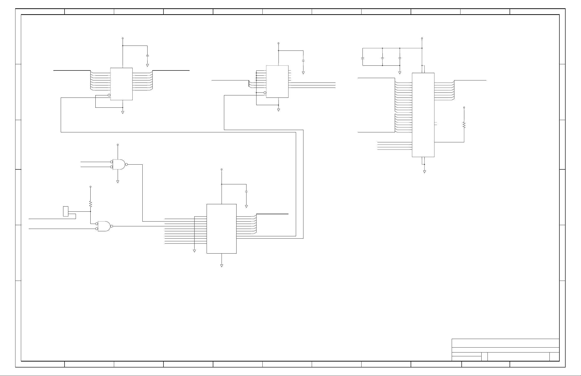
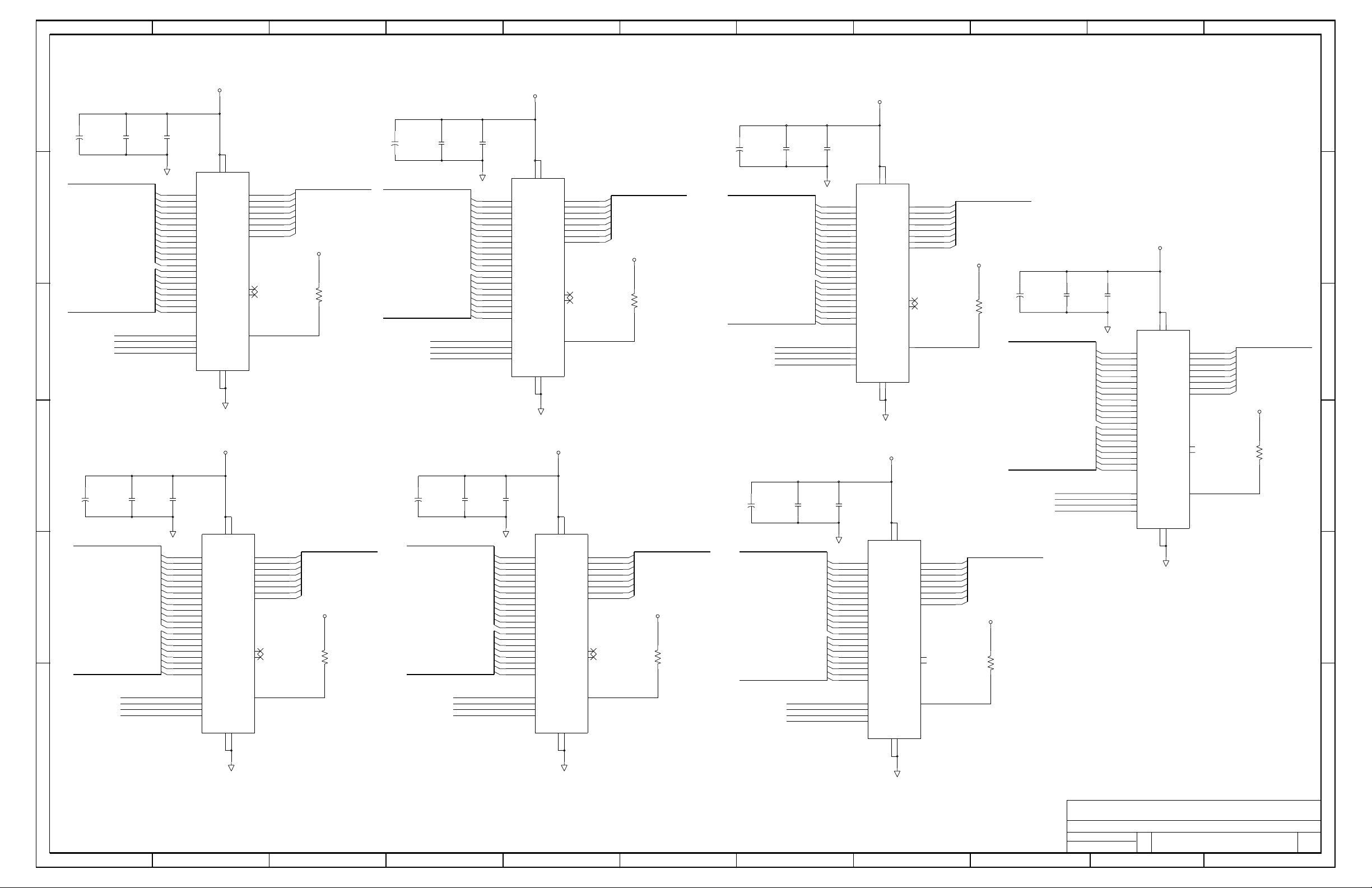
The design titled Paged Flash Disk Using Memory Decode
includes eight flash devices, two latches, two NAND gates,
and a programmable logic device (see attached schematic). Once the software development is done, these flash
devices look like a 16 MB hard drive to a system using
either DOS or Microsoft
Software development using the AMD AM29F016B Flash
Disk has been done with a slightly different hardware
implementation using Datalight’s FlashFX Software Development Kit (SDK) and using DOS as the target platform.
The basics of implementing a flash drive are discusse d in
this application note, but the designer must get both the kit
and the development support from Datalight. FlashFX drivers can be written for DOS, QNX, or Windows CE operating systems. In addition, BIOS extensions can also be
created with the FlashFX software. Various FlashFX software programs have been written and are included in the
SP4GX10 (GX1/CS5530A) development kit. With this software, either a DOS driver or a BIOS extension can be used
to make the flash look like a drive and boot from the flash
device using Datalight’s ROM-DOS. If the flash device is
used as the boot device, there may be problems booting
from a floppy. See Datalight’s website at
www.datalight.com f o r information about FlashFX.
®
Windows® 98 on a FAT16 drive.
2.1 Hardware Implementation
2.1.1 Memory Decode Design: Hardware
The programmable logic device, the Atmel ATF22V10, is
used to decode a memory range window for accessing the
flash. As ISA bus signals SMEMR# and SMEMW# are only
active when the memory range is below 1 MB, a full
decode of all the ISA address lines is not necessary a nd
only ISA address lines SA[19:13] are used to decode the
memory range. The Programmable Logic Device (PLD)
activates one of the eight flash device chip selects when a
memory access between C8000h and C9FFFh occurs,
meaning that at any one time, only an 8 KB region in one of
the flash devices is available. To access another region,
there must be a mechanism for switching to either another
flash device or another 8 KB region in the flash device. The
two transparent latches (74LCX573) and other logic blocks
within the PLD together perform this function. The PLD
also decodes the memory addresses CA000h and
CA001h. When a memory write occurs to CA000h, the
LATCHCS1 signal go es high. When this happens, the output ‘Q’ signals of latch U1 follow the input ‘D’ signals.
These signals are latched on the falling edge. Thus, a
memory write to CA000h causes the data lines to be
latched and sets the upper address signals SA[20:13] on
the flash. Similarly, a memory write to CA001h causes the
lower three data bits of the ISA data bus to be latched and
sets DEC[2:0]. These signals are inputs to the PLD and are
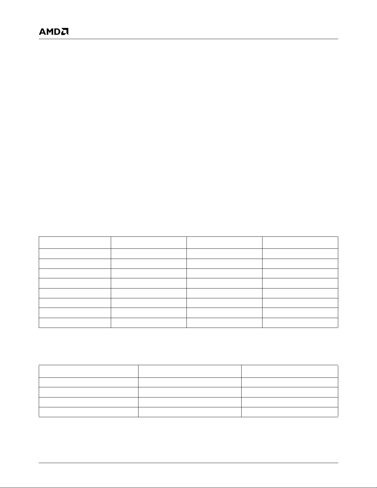
used to select the flash device as shown in Table 2-1 on
page 2.
Note: Since the PLD only uses SA0 to select one of two
Implementation
latches, all other addresses between CA002h and
CBFFFh are duplicates of CA000h and CA001h.
For simplification, it is recommended that only
CA000h and CA001h be used to set the output of
latches U1 and U2. No other software should use
the range CA000h through CBFFFh.
The design titled Paged Flash Disk Using the General Purpose Chip Select includes eight flash devices, one latch,
and a programmable logic device (see attached schematic). These eight flash devices also look like a 16 MB
hard drive with FlashFX software development.
Revision 1.1 - January 2004 - Confidential 1
Page 2
Application Note
Revision 1.1 - January 2004 - Confidential
2.1.2 General Purpose Chip Select Design:
Hardware Implementation
This design is included to show an alternative method of
creating a paged flash disk. It uses less hardware than the
the memory decode design; however, it uses a general purpose chip select output signal from the CS5530A companion device, and depending on the design, an extra chip
select may not be available for use. As in the previous
design, the PLD ATF22V1 0 is used to decode a memory
range window for accessing the flash. As ISA bus signals
SMEMR# and SMEMW# are only active when the memory
range is below 1 MB, a full decode of all the ISA bus signals is not necessary and only ISA address lines SA[19:14]
are used to decode the memory range. The PLD activates
one of the four flash device chip selects when a memory
access between C8000h and CBFFFh occurs. This means
that at any one time, only a 16 KB region in one of the flash
devices can be accessed. The transparent latch
(74LCX573) and PLD are used to select the 16 KB region
and the device. The PLD output, LATCHADDR, is programmed to go low when IOW#, the general purpose chip
select, and the lowest address bit are all low. If the general
Table 2-1. Memory Decode Design: Flash Device Select
DEC2 DEC1 DEC0 Flash Device Selected
purpose chip select has been enabled and configured
through software to respond to writes at 300h and 301h,
when the processor performs an I/O write to address 300h,
the output signal from the PLD LATCHADDR goes high
and the ‘Q’ outputs of the latch follow the inputs ‘D’. On the
falling edge, the data is latched and held until another I/O
write to address 300h occurs. In this manner, software can
select a particular 16 KB memory region for “windowing”.
The registers that select a particular flash device are within
the PLD itself. Output pins 20 and 21 of the PLD U2 in the
schematic are designated latches to select a particular
flash device and hold their values until they are changed
again. The PLD first generates the clock signal called
DECODECLK. This signal goes low when IOW# goes low,
the general purpose chip select goes low, and the lowest
address bit SA0 is high. If the general purpo se chip select
is configured to decode on 300h through 301h, then an I/O
write to 301h causes DECODECLK to go low. The registered outputs DEC0 and DEC1 latch valid data on the rising edge of the clock, DECODECLK. These outputs select
one of four flash devices as described in Table 2-2.
0 0 0 Device #1
0 0 1 Device #2
0 1 0 Device #3
0 1 1 Device #4
1 0 0 Device #5
1 0 1 Device #6
1 1 0 Device #7
1 1 1 Device #8
Table 2-2. General Purpose Chip Select Design: Flash Device Select
DEC1 DEC0 Flash Device Selected
00Device #1
01Device #2
10Device #3
11Device #4
2 AMD Geode™ GX1 Processor Flash Memory Implementation Options and Applications
Page 3

Application Note
Revision 1.1 - January 2004 - Confidential
2.1.3 Equations
Abel Logic for U3
!FL$CS0 = !DEC2 & !DEC1 & !DEC0 & SA19 & SA18 & !SA17 & !SA16_14 & SA15 & !SA13
!FL$CS1 = !DEC2 & !DEC1 & DEC0 & SA19 & SA18 & !SA17 & !SA16_14 & SA15 & !SA13
!FL$CS2 = !DEC2 & DEC1 & !DEC0 & SA19 & SA18 & !SA17 & !SA16_14 & SA15 & !SA13
!FL$CS3 = !DEC2 & DEC1 & DEC0 & SA19 & SA18 & !SA17 & !SA16_14 & SA15 & !SA13
!FL$CS4 = DEC2 & !DEC1 & !DEC0 & SA19 & SA18 & !SA17 & !SA16_14 & SA15 & !SA13
!FL$CS5 = DEC2 & !DEC1 & DEC0 & SA19 & SA18 & !SA17 & !SA16_14 & SA15 & !SA13
!FL$CS6 = DEC2 & DEC1 & !DEC0 & SA19 & SA18 & !SA17 & !SA16_14 & SA15 & !SA13
!FL$CS7 = DEC2 & DEC1 & DEC0 & SA19 & SA18 & !SA17 & !SA16_14 & SA15 & !SA13
LATCHS1 = SA19 & SA18 & !SA17 & !SA16_14 & SA15 & SA13 & !SA0 & !SMEMW
LATCHS2 = SA19 & SA18 & !SA17 & !SA16_14 & SA15 & SA13 & SA0 & !SMEMW
Address
Purpose
C8000h - C9FFFh 8 KB window for accessing the flash memory
Figure 2-1. Memory Decode Design: Hardware Implementation
Abel Logic for U2
!FL$CS0 - !DEC1 & !DEC0 & !AEN & SA19 & SA18 & !SA17 & !SA16 & SA15 & !SA14 & !FLEN
!FL$CS1 - !DEC1 & DEC0 & !AEN & SA19 & SA18 & !SA17 & !SA16 & SA15 & !SA14 & !FLEN
!FL$CS2 - DEC1 & !DEC0 & !AEN & SA19 & SA18 & !SA17 & !SA16 & SA15 & !SA14 & !FLEN
!FL$CS3 - DEC1 & DEC0 & !AEN & SA19 & SA18 & !SA17 & !SA16 & SA15 & !SA14 & !FLEN
LATADDR = !IOW & !GPCS & !SA0
!DECODECLK = !IOW & !GPCS & SA0
DEC1.D - ISASD1;
DEC1.CLK = DECODECLK
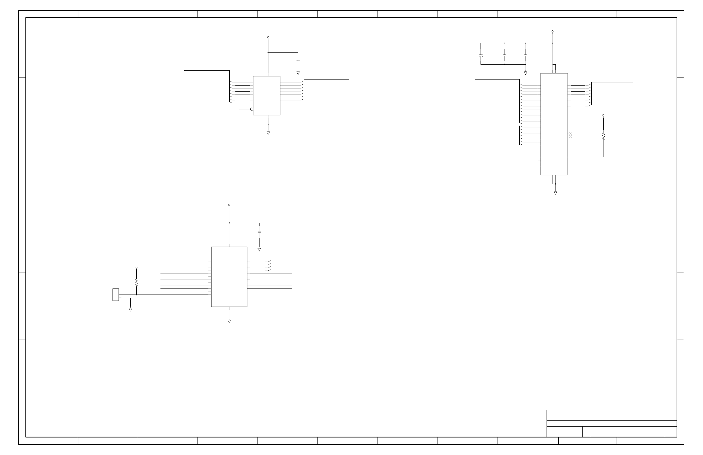
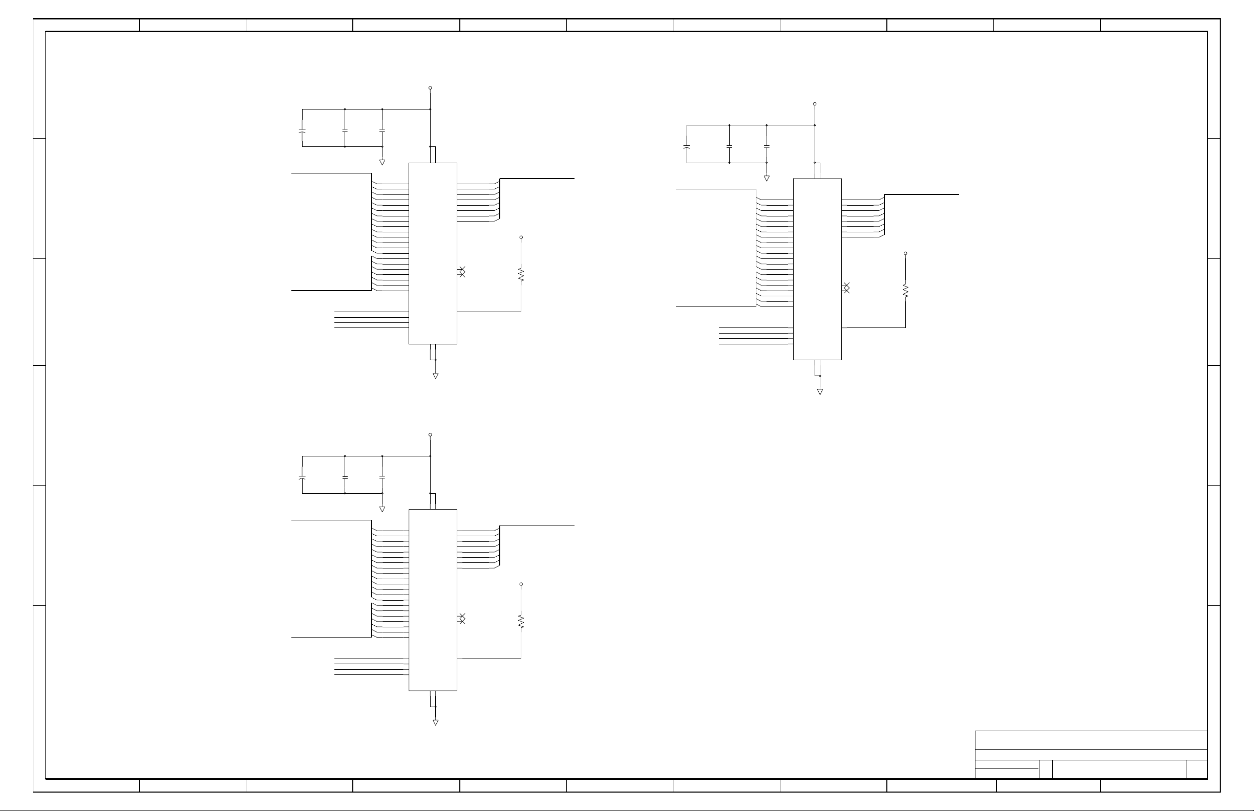
Figure 2-2. General Purpose Chip Select Desi gn: Hardware Implementation
AMD Geode™ GX1 Processor Flash Memory Implementation Options and Applications 3
Page 4

Application Note
Revision 1.1 - January 2004 - Confidential
2.2 Software Implementation
2.2.1 Memory Decode Design: Software Setup
There is no prior setup required for the paged flash disk desig n using me mory decode. The BIOS generally configures the
processor to send all accesses between C8000h and CBFFFh to the PCI bus. These transactions then get passed onto the
ISA bus through the CS5530A and the flash disks exist on the ISA bus. In order to avoid contention on the ISA bus, the user
must not attempt to place a BIOS extension at C8000h through CBFFFh. Similarly, no BIOS extension should be built into
the BIOS that uses the memory range CA000h through CBFFFh.
2.2.2 General Purpose Chip Select Design: Software Setup
Generally, the BIOS sets up the chip selects, but if necessary the software can do this. If using the FlashFX SDK, this
should be done in the mount routine of the Flash Interface Module (FIM). Refer to the FIM code for this implementation as
an example.
2.2.3 Memory Decode Design: Creating FlashFX Software
1) If using the FlashFX SDK, the following variables in file oemconf.h must be modified. These variables determine the
window size and the location of the window range. The variables should be defined as follows.
// Size of window is 8KB.
#defineWINDOW_SIZE1(0x2000L)
// Window Location
#defineWINDOW_ADDRESS1(0x000C8000UL)
2) In the FlashFX SDK, modify the WindowMap() function in file oemhdr.c. This function performs two subfunctions. It cor-
rectly sets the page, selects the flash device (if there is more than one), and returns a pointer to the memor y address
corresponding to ulStart. The parameter called ulStart is simply an offset into the disk. An example WindowMap() function is as follows.
D_UINT WindowMap(D_UINTBIG ulStart)
{
D_UINT uOffset;
D_UCHAR cUpperAddr;
D_UCHAR cFlashSelect;
uOffset = (D_UINT) (ulStart % WindowSize());
// Upper address is bits 13 through 20.
cUpperAddr=(D_UCHAR) ((ulStart>>13)&0xff);
// Flash Select are upper address bits 21 through 23.
cFlashSelect=(D_UCHAR) ((ulStart>>21)&0x07);
ASM .386
ASM push es
ASM push ebx
ASM push eax
// Set the segment register to CA00h.
ASM mov ax,0ca00h
ASM mov es,ax
ASM xor bx,bx
// Latch the upper address bits
ASM mov al,cUpperAddr
ASM mov es:[bx],al
4 AMD Geode™ GX1 Processor Flash Memory Implementation Options and Applications
Page 5

Application Note
Revision 1.1 - January 2004 - Confidential
// Select the flash device.
ASM inc bx
ASM mov al,cFlashSelect
ASM mov es:[bx],al
ASM pop eax
ASM pop ebx
ASM pop es
return (uOffset);
}
3) If using FlashFX SDK, a FIM also must be written. There are four essential functions in this module: mount, write,
erase, and read. These functions are specific to the type of flash being used. At the top of the module there is usually
a list of include and define statements. Assume the following files are included and the following variables are defined.
#include <common.h>
#include <oem.h>
#include <fim.h>
/* Chip sizes - AMD 016 = 2 MB */
#define CHIP_SIZE_016 0x200000L
/* Zone size - 64 KB */
#define ZONE_SIZE 0x10000L
/* AM29F016B ID MFG: 01H Dev: ADH - 8 bit */
#define ID_CODE_016B 0xAD01L
/* Start of Memory Window */
#define WINDOW_START 0C800h
A list of prototypes looks like this:
D_BOOL XAmd016Mount(void);
D_BOOL XAmd016Write(D_UINTBIG ulStart, D_UINT uLength, void D_FAR * lpBuffer);
D_BOOL XAmd016Erase(D_UINTBIG ulStart, D_UINTBIG ulLength);
D_BOOL XAmd016Read(D_UINTBIG ulStart, D_UINT uLength, void D_FAR * lpBuffer);
Device XAmd016 = { XAmd016Mount, ROMUnMount, XAmd016Read, FailRead,
XAmd016Write, FailWrite, XAmd016Erase };
Using the above include statements and defines, the mount function would look like this.
D_BOOL XAmd016Mount(void)
{
D_UINT ulFlashPtr;
D_UINT uId;
D_BOOL bWorked;
ulFlashPtr = (D_UINT) WindowMap(0L);
ASM .386
ASM push es ds edi esi eax ebx ecx edx
// Autoselect Command - Get Device Man. and ID.
ASM mov ax,WINDOW_START
ASM mov es,ax
ASM mov bx, ulFlashPtr
ASM mov BYTE PTR es:[bx], 0xf0
ASM mov BYTE PTR es:[bx], 0xf0
ASM mov BYTE PTR es:[bx + 0x555], 0xaa
ASM mov BYTE PTR es:[bx + 0x2aa], 0x55
ASM mov BYTE PTR es:[bx + 0x555], 0x90
AMD Geode™ GX1 Processor Flash Memory Implementation Options and Applications 5
Page 6

Application Note
Revision 1.1 - January 2004 - Confidential
ASM mov al, BYTE PTR es:[bx]
ASM mov ah, BYTE PTR es:[bx + 1]
ASM mov word ptr uId, ax
// Leave the flash in a read mode
ASM mov BYTE PTR es:[bx], 0xf0
ASM mov BYTE PTR es:[bx], 0xf0
ASM pop edx ecx ebx eax esi edi ds es
if(uId == ID_CODE_016B)
{
lpThisMedia->uDeviceType = DEV_NOR;
lpThisMedia->ulTotalSize = CHIP_SIZE_016;
lpThisMedia->ulTotalPhysicalSize = CHIP_SIZE_016;
lpThisMedia->ulEraseZoneSize = ZONE_SIZE;
lpThisMedia->ulDeviceSize = CHIP_SIZE_016;
lpThisMedia->uInterleaved = NOT_INTERLEAVED;
lpThisMedia->ulWindowSize = WindowSize();
lpThisMedia->uPageSize = 0;
lpThisMedia->uRedundantSize = 0;
bWorked = TRUE;
}
else
{
lpThisMedia->ulTotalSize = 0;
bWorked = FALSE;
}
return bWorked;
}
The following is an example of the write function for the device:
D_BOOL XAmd016Write(D_UINTBIG ulStart, D_UINT uLength, void D_FAR * lpBuffer)
{
D_UINT ulFlashPtr;// Pointer to location to write in flash.
D_UINTBIG ulWindowSize;// Size of window.
D_UINTBIG ulThisLength;// Number of bytes to write within the
// current window.
D_UCHAR D_FAR * lpcDataBuffer;// Pointer to buffer to read data
// from.
D_ASSERT1(ulStart % sizeof(D_UINTBIG) == 0L);
D_ASSERT1(uLength);
D_ASSERT1(lpBuffer);
/*
Verify user address and length parameters within the media
boundaries.
*/
D_ASSERT1((ulStart + uLength) <= lpThisMedia->ulTotalSize);
/* Make some local copies that will be used often */
ulWindowSize = lpThisMedia->ulWindowSize;
lpcDataBuffer = (D_UCHAR D_FAR *) lpBuffer;
D_ASSERT1(ulWindowSize);
6 AMD Geode™ GX1 Processor Flash Memory Implementation Options and Applications
Page 7

Application Note
Revision 1.1 - January 2004 - Confidential
/* Ensure the starting length fits into the first window */
ulThisLength = ulWindowSize - (ulStart % ulWindowSize);
if(uLength < ulThisLength) ulThisLength = (D_UINTBIG) uLength;
/* Move each window worth of data into the flash memory */
while(uLength)
{
ulFlashPtr = (D_UINT) WindowMap(ulStart);
ASM .386
ASM push es ds edi esi eax ebx ecx edx
// Pointer into the flash array
ASM mov ax, WINDOW_START
ASM mov es, ax
ASM mov di, WORD PTR ulFlashPtr
// Get the address of the client data buffer
ASM lds si, lpcDataBuffer
// Now DS:SI points to the client buffer
// and ES:DI points to the flash array
// Program loop
ASM mov cx, ulThisLength program_loop:
/* Get the byte and setup the command address */
ASM mov al, BYTE PTR ds:[si]
ASM mov bx, WORD PTR ulFlashPtr
ASM and bx, 0xF000
// Write command sequence coded in-line since timing
// critical.
ASM mov BYTE PTR es:[bx + 0x555], 0xaa
ASM mov BYTE PTR es:[bx + 0x2aa], 0x55
ASM mov BYTE PTR es:[bx + 0x555], 0xa0
ASM mov BYTE PTR es:[di], al
/*
*/
wait_loop1:
ASM mov al, BYTE PTR ds:[si]
ASM mov ah, BYTE PTR es:[di]
ASM mov bl, ah
// AL - client byte, AH - flash byte
ASM and al, 0x80
ASM and ah, 0x80
ASM cmp al, ah
ASM je ok1
Wait till the byte is done programming indicated when data bit 7 is the same
as the data bit 7 being written.
/*
Check for error indicated when bit 5 set and bit 7 isn't right
AMD Geode™ GX1 Processor Flash Memory Implementation Options and Applications 7
Page 8

*/
ASM and bl, 0x20
ASM jz wait_loop1
ASM pop edx ecx ebx eax esi edi ds es
ASM jmp FailProgram
ok1:
// Increment to next byte
ASM inc di
ASM inc si
ASM dec cx
ASM or cx, cx
ASM jz done_loop
ASM jmp program_loop
done_loop:
ASM pop edx ecx ebx eax esi edi ds es
/* Go to the next offset */
ulStart += ulThisLength;
lpcDataBuffer += (D_UINT) ulThisLength;
Application Note
Revision 1.1 - January 2004 - Confidential
} /* while end */
/* Return success if all bytes were written correctly */
return TRUE;
{
FailProgram:
}
}
uLength -= (D_UINT) ulThisLength;
D_ASSERT1(ulStart);
/* Recalculate the length of the next request */
if(uLength < ulWindowSize)
ulThisLength = (D_UINTBIG) uLength;
else
ulThisLength = ulWindowSize;
/* Clear the error status, reset to read mode and return */
ASM push es ds edi esi eax ebx ecx edx
ASM mov ax,WINDOW_START
ASM mov es, ax
ASM mov bx, WORD PTR ulFlashPtr
ASM mov BYTE PTR es:[bx], 0xf0
ASM pop edx ecx ebx eax esi edi ds es
return FALSE;
8 AMD Geode™ GX1 Processor Flash Memory Implementation Options and Applications
Page 9

Application Note
Revision 1.1 - January 2004 - Confidential
The following function erases sections of the flash device:
D_BOOL XAmd016Erase(D_UINTBIG ulStart, D_UINTBIG ulLength)
{
D_UINT ulFlashPtr;
D_UCHAR bStatus1;
do {
ulFlashPtr = (D_UINT) WindowMap(ulStart);
ASM .386
ASM push es ds edi esi eax ebx ecx edx
ASM mov ax,WINDOW_START
ASM mov es,ax
ASM mov bx, ulFlashPtr
ASM and bx, 0F000h
// Reset flash device.
ASM mov BYTE PTR es:[bx], 0xf0
ASM mov BYTE PTR es:[bx], 0xf0
// Issue sector erase command.
ASM mov BYTE PTR es:[ bx + 0x555 ], 0xaa
ASM mov BYTE PTR es:[ bx + 0x2aa ], 0x55
ASM mov BYTE PTR es:[ bx + 0x555 ], 0x80
ASM mov BYTE PTR es:[ bx + 0x555 ], 0xaa
ASM mov BYTE PTR es:[ bx + 0x2aa ], 0x55
ASM mov BYTE PTR es:[ bx ], 0x30
waitloop1:
ASM mov al, BYTE PTR es:[bx]
ASM mov bStatus1, al
ASM cmp al,0xFF
ASM je okay1
ASM and al,0x20
ASM jz waitloop1
FailErase1:
ASM mov al, BYTE PTR es:[bx]
ASM mov bStatus1, al
ASM cmp al,0xFF
ASM jz okay1
ASM pop edx ecx ebx eax esi edi ds es
ASM jmp FailedErase
okay1:
ASM pop edx ecx ebx eax esi edi ds es
/* Go to the next block */
ulStart += lpThisMedia->ulEraseZoneSize;
ulLength -= lpThisMedia->ulEraseZoneSize;
D_ASSERT1(ulStart);
/* Leave the block in read mode */
ASM push es ds edi esi eax ebx ecx edx
ASM mov ax,WINDOW_START
ASM mov es, ax
ASM mov bx, ulFlashPtr
ASM mov BYTE PTR es:[bx], 0xf0
ASM pop edx ecx ebx eax esi edi ds es
AMD Geode™ GX1 Processor Flash Memory Implementation Options and Applications 9
Page 10

Revision 1.1 - January 2004 - Confidential
} while ( ulLength );
/* Erase worked */
return TRUE;
FailedErase:
/* Leave the block in read mode */
ASM push es ds edi esi eax ebx ecx edx
ASM mov ax,WINDOW_START
ASM mov es, ax
ASM mov bx, ulFlashPtr
ASM mov BYTE PTR es:[bx], 0xf0
ASM pop edx ecx ebx eax esi edi ds es
return FALSE;
}
The following function performs a read of the flash device.
D_BOOL XAmd016Read(D_UINTBIG ulStart, D_UINT uLength, void D_FAR * lpBuffer)
{
D_UINTBIG ulWindowSize;
D_UINT uThisLength;
D_UINT FlashPtr;
D_UCHAR D_FAR * lpcBuffer;
Application Note
D_ASSERT1(ulStart < MAX_ARRAY);
D_ASSERT1(uLength);
D_ASSERT1(lpBuffer);
/* Make some local copies that will be used often */
lpcBuffer = (D_UCHAR D_FAR *) lpBuffer;
ulWindowSize = WindowSize();
D_ASSERT1(ulWindowSize);
/* Ensure the starting length fits into the first window */
uThisLength = (D_UINT) (ulWindowSize - (ulStart % ulWindowSize));
if(uLength < uThisLength)
uThisLength = uLength;
/* Move each window worth of data into the client buffer */
while(uLength)
{
/* Update the flash pointer */
FlashPtr = (D_UINT) WindowMap(ulStart);
D_ASSERT1(FlashPtr);
ASM .386
ASM push es ds ecx edi esi eax
// Get the length
ASM XOR ecx, ecx
ASM mov cx, uThisLength
ASM shr ecx, 2 // Change the length to dwords.
10 AMD Geode™ GX1 Processor Flash Memory Implementation Options and Applications
Page 11

Application Note
Revision 1.1 - January 2004 - Confidential
// Get the client data buffer
ASM les di, DWORD PTR lpcBuffer
// DS points to paged memory window.
ASM mov si, FlashPtr
ASM mov ax, WINDOW_START
ASM mov ds, ax
// ES:DI points to the buffer
// DS:SI points to the flash,
// Move up in memory
ASM cld
// Perform the read!
ASM rep movs DWORD PTR es:[di], DWORD PTR ds:[si]
ASM pop eax esi edi ecx ds es
/* Go to the next offset */
ulStart += uThisLength;
lpcBuffer += uThisLength;
uLength -= uThisLength;
/* Recalculate the length of the next request */
if(uLength < ulWindowSize)
uThisLength = uLength;
else
uThisLength = (D_UINT) ulWindowSize;
// Update flash pointer.
FlashPtr = (D_UINT) WindowMap(ulStart);
}
/* ROM Read always works */
return TRUE;
}
2.2.4 General Purpose Chip Select Design: Creating FlashFX Software
1) Variables in oemconf.h should be modified as follows.
// Size of window is 16KB.
#define WINDOW_SIZE1(0x4000L)
// Window Location
#define WINDOW_ADDRESS1(0x000C8000UL)
An example WindowMap() function for this design is:
void D_FAR * D_PASCAL WindowMap(D_UINTBIG ulStart)
{
D_UINT uOffset;
D_UCHAR cUpperAddr;
D_UCHAR cFlashSelect;
uOffset = (D_UINT) (ulStart % WindowSize());
// Upper address is bits 14 through 20.
cUpperAddr=(D_UCHAR) ((ulStart>>14)&0x7f);
// Flash Select are upper address bits 21 and 22.
cFlashSelect=(D_UCHAR) ((ulStart>>21)&0x03);
AMD Geode™ GX1 Processor Flash Memory Implementation Options and Applications 11
Page 12

Application Note
Revision 1.1 - January 2004 - Confidential
ASM .386
ASM push edx
ASM push eax
// Latch the upper address bits
ASM mov dx,0300h
ASM mov al,cUpperAddr
ASM out dx,al
// Select flash device to access.
ASM inc dx
ASM mov al,cFlashSelect
ASM out dx,al
ASM pop eax
ASM pop edx
return (void D_FAR *)(WINDOW_ADDRESS1 + uOffset);
}
2) All the FIMs for this design are identical to those for the memory decode design except for the mount function. In the
mount function, the general purpose chip sel ect must be configured. The following is the mount function and the extra
defines that must be added.
// Use the following address to access the general purpose chip select
// register if HOLDREQ# is tied low; otherwise, if HOLDREQ# is tied
// high, use 080008070h.
#define GPCS_CONFIG_ADD 080009070h
// Index 70-71: General Purpose Chip Select IO Base Address
// Index 72:
// Bit 7 = 1 Enable chip select
// Bit 6 = 1 Enable on writes
// Bit 5 = 0 Disable on reads
// Bits 4:0 = 00001 Range is two bytes.
#define GPCS_CONFIG_DATA 000c10300h
D_BOOL XAmd016Mount(void)
{
D_UINT ulFlashPtr;
D_UINT uId;
D_BOOL bWorked;
// Before setting up the flash address, the general
// purpose chip select should be configured so that
// the chip select is enabled on writes to 0x300
// and 0x301. This must occur before the WindowMap()
// function!
ASM .386
ASM push eax edx
// Latch address.
ASM mov dx,0cf8h
ASM mov eax,GPCS_CONFIG_ADD
ASM out dx,eax
12 AMD Geode™ GX1 Processor Flash Memory Implementation Options and Applications
Page 13

Application Note
Revision 1.1 - January 2004 - Confidential
// Write data to Indices 70h-73h
ASM mov dx,0cfch
ASM mov eax,GPCS_CONFIG_DATA
ASM out dx,eax
ASM pop edx eax
ulFlashPtr = (D_UINT) WindowMap(0L);
ASM .386
ASM push es ds edi esi eax ebx ecx edx
// Autoselect Command - Get Device Man. and ID.
ASM mov ax,WINDOW_START
ASM mov es,ax
ASM mov bx, ulFlashPtr
ASM mov BYTE PTR es:[bx], 0xf0
ASM mov BYTE PTR es:[bx], 0xf0
ASM mov BYTE PTR es:[bx + 0x555], 0xaa
ASM mov BYTE PTR es:[bx + 0x2aa], 0x55
ASM mov BYTE PTR es:[bx + 0x555], 0x90
{
}
}
ASM mov al, BYTE PTR es:[bx]
ASM mov ah, BYTE PTR es:[bx + 1]
ASM mov word ptr uId, ax
// Leave the flash in a read mode
ASM mov BYTE PTR es:[bx], 0xf0
ASM mov BYTE PTR es:[bx], 0xf0
ASM pop edx ecx ebx eax esi edi ds es
if(uId == ID_CODE_016B)
lpThisMedia->uDeviceType = DEV_NOR;
lpThisMedia->ulTotalSize = CHIP_SIZE_016;
lpThisMedia->ulTotalPhysicalSize = CHIP_SIZE_016;
lpThisMedia->ulEraseZoneSize = ZONE_SIZE;
lpThisMedia->ulDeviceSize = CHIP_SIZE_016;
lpThisMedia->uInterleaved = NOT_INTERLEAVED;
lpThisMedia->ulWindowSize = WindowSize();
lpThisMedia->uPageSize = 0;
lpThisMedia->uRedundantSize = 0;
bWorked = TRUE;
else
{
lpThisMedia->ulTotalSize = 0;
bWorked = FALSE;
}
return bWorked;
AMD Geode™ GX1 Processor Flash Memory Implementation Options and Applications 13
Page 14
1011
9
5678
234
1
F
F
* REFERENCE DESIGN *
E
16 MB PAGED FLASH DISK IMPLEMENTATION
E
USING MEMORY DECODE
D
D
C
B
A
C
B
A
AMD
TITLE:
TITLE PAGE
SCALE:
OFPG.
11
910
78 56
DWG
DWG NO.
SIZE
C
31
243
PAGED FLASH DISK
WITH MEMORY DECODE
1351 S. SUNSET STREET
LONGMONT, CO 80501
1
REV
1.0
Page 15
1011
9
5678
234
1
F
E
D
J1
ON FLASH DEVICES ENABLED
FLASH DEVICES DISABLED
OFF
C
ISA$SA<17>
ISA$AEN
B
LATCHCS1
J1
HDR
2
1
0
1
2
3
4
5
6
7
ISA$SA<16>
ISA$SA<14>
VCC3V
2
R1
22K
1
4
5
VCC3V
1
C1
0.1UF
2
20
U1
2
D0
3
D1
4
D2
5
D3
6
D4
7
D5
8
D6
9
D7
1 11
OC*
11
G
VCC3V
U12
1
2
74LCX32
714
SSOP14_65MM
19
Q0
VCC
18
Q1
17
Q2
16
Q3
15
Q4
14
Q5
13
Q6
12
Q7
GND
74LCX573
10
TSSOP20_65MM
3
13
14
15
16
17
18
19
20
FL$SA<20..13>ISA$SD<7..0>
ISA$SD<7..0> ISA$SD<7..0>
LATCHCS2
VCC5V
1
2
U3
U12
6
74LCX32
SSOP14_65MM
1
ISA$SA<13>
ISA$SA16_14
ISA$SA<15>
FL$SA<17>
ISA$SA<18>
ISA$SA<19>
ISA$SA<0>
ISA$SMEMW* LATCHCS1
DEC2
DEC1
DEC0
CLK/IN0
2
IN1
3
IN2
4
IN3
5
IN4
6
IN5
7
IN6
8
IN7
9
IN8
10
IN9
11
IN10
13
IN11
I/O0
I/O1
I/O2
I/O3
I/O4
I/O5
I/O6
I/O7
I/O8
I/O9
14
15
16
17
18
19
20
21
22
23
GND VCC
ATF22V10CZ-15PC
12 24
DP24SKT
2
1
0
C2
0.1UF
0
1
2
3
4
5
6
7
2
D0
3
D1
4
D2
5
D3
6
D4
7
D5
8
D6
9
D7
1
OC*
G
FL$CS<7..0>
LATCHCS2
VCC3V
20
Q0
VCC
Q1
Q2
Q3
Q4
Q5
Q6
Q7
GND
74LCX573
10
TSSOP20_65MM
U2
VCC5V
1
C20
1
C3
0.1UF
2
19
18
17
16
15
14
DEC2
13
DEC1
12
DEC0
+
2.2UF
10V
TANT
2
ISA$SA<12..0>
1
2
C4
0.1UF
FL$SA<20..13>
ISA$SMEMW*
FL$CS<0>
PCI$RST*
0
1
2
3
4
5
6
7
8
9
10
11
12
13
14
15
16
17
18
19
20
1
2
C5
0.1UF
24
23
22
21
20
19
18
17
16
15
14
13
40
37
38
12
FLASH DEVICE #1
31
10
U4
VCC
VCC
A0
A1
A2
A3
A4
A5
A6
A7
A8
A9
A10
A11
8
A12
7
A13
6
A14
5
A15
4
A16
3
A17
2
A18
1
A19
A20
OE
WE
9
CE
RST*
GND
29
25
D0
26
D1
27
D2
28
D3
32
D4
33
D5
34
D6
35
D7
39
NC
11
NC
36
RDY
GND
AM29F016B-120E4C
TSOP40_5MM
30
0
1
2
3
4
5
6
7
VCC5V
2
R2
22K
1
FLSH$RDYISA$SMEMR*
F
E
D
EACH AMD FLASH DEVICE IS 2 MEGABYTES.
C
B
DEC2 THROUGH DEC0 SELECT ONE OF EIGHT CHIP SELECTS TO GO LOW.
ABEL LOGIC FOR U3
!FL$CS0 = !DEC2 & !DEC1 & !DEC0 & SA19 & SA18 & !SA17 & !SA16_14 & SA15 & !SA13
!FL$CS1 = !DEC2 & !DEC1 & DEC0 & SA19 & SA18 & !SA17 & !SA16_14 & SA15 & !SA13
!FL$CS2 = !DEC2 & DEC1 & !DEC0 & SA19 & SA18 & !SA17 & !SA16_14 & SA15 & !SA13
!FL$CS3 = !DEC2 & DEC1 & DEC0 & SA19 & SA18 & !SA17 & !SA16_14 & SA15 & !SA13
A
!FL$CS4 = DEC2 & !DEC1 & !DEC0 & SA19 & SA18 & !SA17 & !SA16_14 & SA15 & !SA13
ADDRESS
-------------------------------C8000 - C9FFF 8KB WINDOW FOR ACCESSING THE FLASH MEMORY
PURPOSE
CA000 WRITE ONE BYTE HERE IN ORDER TO LATCH UPPER ADDRESS BITS
CA001 WRITE ONE BYTE HERE IN ORDER TO SELECT THE PARTICULAR FLASH DEVICE
CA002-CBFFF DO NOT WRITE ANYTHING HERE - MEMORY LOCATIONS CA000 AND CA001
ARE DUPLICATED HERE
A
!FL$CS5 = DEC2 & !DEC1 & DEC0 & SA19 & SA18 & !SA17 & !SA16_14 & SA15 & !SA13
!FL$CS6 = DEC2 & DEC1 & !DEC0 & SA19 & SA18 & !SA17 & !SA16_14 & SA15 & !SA13
!FL$CS7 = DEC2 & DEC1 & DEC0 & SA19 & SA18 & !SA17 & !SA16_14 & SA15 & !SA13
LATCHCS1 = SA19 & SA18 & !SA17 & !SA16_14 & SA15 & SA13 & !SA0 & !SMEMW
LATCHCS2 = SA19 & SA18 & !SA17 & !SA16_14 & SA15 & SA13 & SA0 & !SMEMW
11
910
78 56
AMD
TITLE:
PLD, LATCHES, AND FLASH
SCALE:
OFPG.
32
DWG
SIZE
C
243
DWG NO.
PAGED FLASH DISK
WITH MEMORY DECODE
1351 S. SUNSET STREET
LONGMONT, CO 80501
1
REV
1.0
Page 16
1011
9
5678
234
1
F
E
D
C
1
C21
+
2.2UF
10V
TANT
2
ISA$SA<12..0>
FL$SA<20..13>
ISA$SMEMW*
1
0.1UFC60.1UF
2
0
1
2
3
4
5
6
7
8
9
10
11
12
13
14
15
16
17
18
19
20
FL$CS<1>
PCI$RST*
VCC5V
1
C8
2
24
A0
23
A1
22
A2
21
A3
20
A4
19
A5
18
A6
17
A7
16
A8
15
A9
14
A10
13
A11
8
A12
7
A13
6
A14
5
A15
4
A16
3
A17
2
A18
1
A19
40
A20
37
OE
38
WE
9
CE
12
RST*
FLASH DEVICE #2
10
31
U5
VCC
VCC
GND
29
VCC5V
25
D0
26
D1
27
D2
28
D3
32
D4
33
D5
34
D6
35
D7
39
NC
11
NC
36
RDY
GND
AM29F016B-120E4C
TSOP40_5MM
30
FLSH$RDYISA$SMEMR*
0
1
2
3
4
5
6
7
ISA$SD<7..0>
VCC5V
R3
22K
1
1
C23
+
2.2UF
10V
TANT
2
ISA$SA<12..0>
FL$SA<20..13>
ISA$SMEMW*
1
C10
0.1UF
2
FL$CS<2>
PCI$RST*
0
1
2
3
4
5
6
7
8
9
10
11
12
13
14
15
16
17
18
19
20
1
2
C12
0.1UF
VCC5V
1
FLASH DEVICE #3
10
31
U7
VCC
A0
A1
A2
A3
A4
A5
A6
A7
A8
A9
A10
A11
A12
A13
A14
A15
A16
A17
A18
A19
A20
OE
WE
CE
RST*
VCC
GND
29
GND
30
D0
D1
D2
D3
D4
D5
D6
D7
NC
NC
RDY
VCC5V
25
26
27
28
32
33
34
35
39
11
36
AM29F016B-120E4C
TSOP40_5MM
24
23
22
21
20
19
18
17
16
15
14
13
8
7
6
5
4
3
2
1
40
37
38
9
12
0
1
2
3
4
5
6
7
FLSH$RDYISA$SMEMR*
ISA$SD<7..0>
VCC5V
2
R5
22K
1
C25
+
2.2UF
10V
TANT
2
ISA$SA<12..0>
FL$SA<20..13>
1
C14
0.1UF
2
ISA$SMEMR*
ISA$SMEMW*
FL$CS<3>
PCI$RST*
0
1
2
3
4
5
6
7
8
9
10
11
12
13
14
15
16
17
18
19
20
1
2
C16
0.1UF
VCC5V
FLASH DEVICE #4
10
31
U9
VCC
A0
A1
A2
A3
A4
A5
A6
A7
A8
A9
A10
A11
A12
A13
A14
A15
A16
A17
A18
A19
A20
OE
WE
CE
RST*
VCC
24
23
22
21
20
19
18
17
16
15
14
13
8
7
6
5
4
3
2
1
40
37
38
9
12
GND
29
VCC5V
25
D0
26
D1
27
D2
28
D3
32
D4
33
D5
34
D6
35
D7
39
NC
11
NC
36
RDY
GND
AM29F016B-120E4C
TSOP40_5MM
30
0
1
2
3
4
5
6
7
FLSH$RDY
ISA$SD<7..0>
VCC5V
2
R7
22K
1
1
C27
+
2.2UF
10V
TANT
2
ISA$SA<12..0>
FL$SA<20..13>
12
2
C18
0.1UF
0
1
2
3
4
5
6
7
8
9
10
11
12
13
14
15
16
17
18
19
20
1
2
C19
0.1UF
24
23
22
21
20
19
18
17
16
15
14
13
40
VCC5V
FLASH DEVICE #5
10
31
U11
VCC
VCC
A0
A1
A2
A3
A4
A5
A6
A7
A8
A9
A10
A11
8
A12
7
A13
6
A14
5
A15
4
A16
3
A17
2
A18
1
A19
A20
D0
D1
D2
D3
D4
D5
D6
D7
NC
NC
25
26
27
28
32
33
34
35
39
11
0
1
2
3
4
5
6
7
ISA$SD<7..0>
VCC5V
2
R9
22K
1
F
E
D
C
1
C22
+
2.2UF
10V
TANT
2
ISA$SA<12..0>
B
FL$SA<20..13>
A
11
1
2
ISA$SMEMW*
FL$CS<5> FL$CS<6>
PCI$RST*
C7
0.1UF
0
1
2
3
4
5
6
7
8
9
10
11
12
13
14
15
16
17
18
19
20
1
2
C9
0.1UF
24
23
22
21
20
19
18
17
16
15
14
13
40
37
38
12
10
31
U6
VCC
VCC
A0
A1
A2
A3
A4
A5
A6
A7
A8
A9
A10
A11
8
A12
7
A13
6
A14
5
A15
4
A16
3
A17
2
A18
1
A19
A20
OE
WE
9
CE
RST*
GND
29
25
D0
26
D1
27
D2
28
D3
32
D4
33
D5
34
D6
35
D7
39
NC
11
NC
36
RDY
GND
AM29F016B-120E4C
TSOP40_5MM
30
0
1
2
3
4
5
6
7
FLSH$RDYISA$SMEMR*
ISA$SD<7..0>
VCC5V
2
R4
22K
1
910
1
C24
+
2.2UF
10V
TANT
2
ISA$SA<12..0>
FL$SA<20..13>
ISA$SMEMW*
1
C11
0.1UF
2
PCI$RST*
0
1
2
3
4
5
6
7
8
9
10
11
12
13
14
15
16
17
18
19
20
1
2
C13
0.1UF
24
23
22
21
20
19
18
17
16
15
14
13
40
37
38
12
1
FLASH DEVICE #7FLASH DEVICE #6
10
31
U8
VCC
VCC
A0
A1
A2
A3
A4
A5
A6
A7
A8
A9
A10
A11
8
A12
7
A13
6
A14
5
A15
4
A16
3
A17
2
A18
1
A19
A20
OE
WE
9
CE
RST*
GND
29
25
D0
26
D1
27
D2
28
D3
32
D4
33
D5
34
D6
35
D7
39
NC
11
NC
36
RDY
GND
AM29F016B-120E4C
TSOP40_5MM
30
0
1
2
3
4
5
6
7
VCC5V
2
R6
22K
1
FLSH$RDYISA$SMEMR*
C26
+
2.2UF
10V
TANT
2
ISA$SA<12..0>ISA$SD<7..0>
FL$SA<20..13>
1
C15
0.1UF
2
ISA$SMEMW*
FL$CS<7>
PCI$RST*
0
1
2
3
4
5
6
7
8
9
10
11
12
13
14
15
16
17
18
19
20
1
2
C17
0.1UF
24
23
22
21
20
19
18
17
16
15
14
13
40
37
38
12
FLASH DEVICE #8
10
31
U10
VCC
VCC
A0
A1
A2
A3
A4
A5
A6
A7
A8
A9
A10
A11
8
A12
7
A13
6
A14
5
A15
4
A16
3
A17
2
A18
1
A19
A20
OE
WE
9
CE
RST*
GND
29
25
D0
26
D1
27
D2
28
D3
32
D4
33
D5
34
D6
35
D7
39
NC
11
NC
36
RDY
GND
AM29F016B-120E4C
TSOP40_5MM
30
0
1
2
3
4
5
6
7
FLSH$RDYISA$SMEMR*
ISA$SD<7..0>
VCC5V
2
R8
22K
1
ISA$SMEMR*
ISA$SMEMW*
FL$CS<4>
PCI$RST*
AMD
TITLE:
SEVEN FLASH DEVICES
SCALE:
78 56
37
OE
38
WE
9
CE
12
RST*
GND
29
36
RDY
GND
AM29F016B-120E4C
TSOP40_5MM
30
FLSH$RDY
B
A
1351 S. SUNSET STREET
LONGMONT, CO 80501
DWG
DWG NO.
OFPG.
SIZE
C
33
243
PAGED FLASH DISK
WITH MEMORY DECODE
1
REV
1.0
Page 17
1011
9
5678
234
1
F
E
* REFERENCE DESIGN *
F
E
8 MB PAGED FLASH DISK IMPLEMENTATION
USING THE GENERAL PURPOSE CHIP SELECT
D
D
C
B
A
C
B
A
AMD
TITLE:
TITLE PAGE
SCALE:
OFPG.
11
910
78 56
DWG
SIZE
C
DWG NO.
243
1351 S. SUNSET STREET
LONGMONT, CO 80501
1
REV
1.0PAGED FLASH WITH GPCS*31
Page 18
1011
9
5678
234
1
VCC3V
F
1
C300
+
1
C10
0.1UF
ISA$SD<7..0>
2
0
3
1
4
2
5
3
6
4
7
5
8
6
9
7
1
E
LATCHADDR
11
D0
D1
D2
D3
D4
D5
D6
D7
OC*
G
20
U5
Q0
VCC
Q1
Q2
Q3
Q4
Q5
Q6
Q7
GND
74LCX573
10
TSSOP20_65MM
2
19
14
18
15
17
16
16
17
15
18
14
19
13
20
12
FL$SA<20..14>
THIS LATCH IS USED FOR PAGING.
2.2UF
10V
TANT
2
ISA$SA<13..0>
FL$SA<20..14>
D
1
2
ISA$SMEMR* FLSH$RDY
ISA$SMEMW*
FL$CS<0>
PCI$RST*
C303
0.1UF
0
1
2
3
4
5
6
7
8
9
10
11
12
13
14
15
16
17
18
19
20
1
2
C293
0.1UF
VCC5V
F
FLASH DEVICE #1
10
31
U3
VCC
A0
A1
A2
A3
A4
A5
A6
A7
A8
A9
A10
A11
A12
A13
A14
A15
A16
A17
A18
A19
A20
OE
WE
CE
RST*
VCC
GND
29
GND
30
D0
D1
D2
D3
D4
D5
D6
D7
NC
NC
RDY
25
26
27
28
32
33
34
35
39
11
36
AM29F016B-120E4C
TSOP40_5MM
24
23
22
21
20
19
18
17
16
15
14
13
8
7
6
5
4
3
2
1
40
37
38
9
12
0
1
2
3
4
5
6
7
ISA$SD<7..0>
VCC5V
2
R320
22K
1
E
D
VCC5V
C
DECODECLK
VCC3V
2
R4
J1
1
2
B
HDR
22K
1
ISA$SA<14>
ISA$SA<15>
ISA$SA<16>
ISA$SA<17>
ISA$SA<18>
ISA$SA<19>
ISA$AEN
ISA$SD<1>
ISA$SD<0>
ISA$SA<0>
FL$EN*
1
2
3
4
5
6
7
8
9
10
11
13
CLK/IN0
IN1
IN2
IN3
IN4
IN5
IN6
IN7
IN8
IN9
IN10
IN11
2412
GND VCC
16 KB WINDOW AT C8000.
1
C420
0.1UF
2
U2
0
1
2
3
FL$CS<3..0>
14
I/O0
15
I/O1
16
I/O2
17
I/O3
18
I/O4
19
I/O5
20
I/O6
21
I/O7
22
I/O8
23
I/O9
ATF22V10CZ-15PC
DP24SKT
LATCHADDR
DECODECLK
DEC1
DEC0
ISA$IOW*
GPCS*
ABEL LOGIC FOR U2
!FL$CS0 = !DEC1 & !DEC0 & !AEN & SA19 & SA18 & !SA17 & !SA16 & SA15 & !SA14 & !FLEN
!FL$CS1 = !DEC1 & DEC0 & !AEN & SA19 & SA18 & !SA17 & !SA16 & SA15 & !SA14 & !FLEN
!FL$CS2 = DEC1 & !DEC0 & !AEN & SA19 & SA18 & !SA17 & !SA16 & SA15 & !SA14 & !FLEN
!FL$CS3 = DEC1 & DEC0 & !AEN & SA19 & SA18 & !SA17 & !SA16 & SA15 & !SA14 &!FLEN
LATCHADDR = !IOW & !GPCS & !SA0
!DECODECLK = !IOW & !GPCS & SA0
DEC1.D = ISASD1;
DEC1.CLK = DECODECLK
DEC0.D = ISASD0;
DEC0.CLK = DECODECLK
EACH AMD DEVICE IS 2 MEGABYTES IN SIZE
C
B
J1
ON FLASH DEVICES ENABLED
FLASH DEVICES DISABLED
OFF
THIS PLD DECODES MEMORY ACCESSES BETWEEN C8000 AND CBFFF
DEC2 THROUGH DEC0 SELECT ONE OF EIGHT CHIP SELECTS TO GO LOW.
A
AMD
TITLE:
MEMORY WINDOW DECODE AND ONE FLASH DEVICE
SCALE:
OFPG.
11
910
78 56
DWG
SIZE
C
DWG NO.
243
1351 S. SUNSET STREET
LONGMONT, CO 80501
1
A
REV
1.0PAGED FLASH DISK USING GPCS*32
Page 19
1011
9
5678
234
1
F
1
+
2
C7
2.2UF
10V
TANT
1
0.1UFC40.1UF
2
1
C1
2
ISA$SA<13..0>
0
1
2
E
FL$SA<20..14>
3
4
5
6
7
8
9
10
11
12
13
14
15
16
17
18
19
20
D
ISA$SMEMW*
FL$CS<1>
PCI$RST*
VCC5V
VCC5V
FLASH DEVICE #2
10
31
U34
VCC
A0
A1
A2
A3
A4
A5
A6
A7
A8
A9
A10
A11
A12
A13
A14
A15
A16
A17
A18
A19
A20
OE
WE
CE
RST*
VCC
GND
29
GND
30
D0
D1
D2
D3
D4
D5
D6
D7
NC
NC
RDY
25
26
27
28
32
33
34
35
39
11
36
AM29F016B-120E4C
TSOP40_5MM
24
23
22
21
20
19
18
17
16
15
14
13
8
7
6
5
4
3
2
1
40
37
38
9
12
0
1
2
3
4
5
6
7
FLSH$RDYISA$SMEMR*
ISA$SD<7..0>
VCC5V
2
R1
22K
1
1
C9
+
2.2UF
10V
TANT
2
ISA$SA<13..0>
FL$SA<20..14>
ISA$SMEMW*
1
0.1UFC60.1UF
2
0
1
2
3
4
5
6
7
8
9
10
11
12
13
14
15
16
17
18
19
20
FL$CS<3>
PCI$RST*
1
C3
2
24
A0
23
A1
22
A2
21
A3
20
A4
19
A5
18
A6
17
A7
16
A8
15
A9
14
A10
13
A11
8
A12
7
A13
6
A14
5
A15
4
A16
3
A17
2
A18
1
A19
40
A20
37
OE
38
WE
9
CE
12
RST*
FLASH DEVICE #4
10
31
U4
VCC
VCC
GND
29
25
D0
26
D1
27
D2
28
D3
32
D4
33
D5
34
D6
35
D7
39
NC
11
NC
36
RDY
GND
AM29F016B-120E4C
TSOP40_5MM
30
0
1
2
3
4
5
6
7
FLSH$RDYISA$SMEMR*
ISA$SD<7..0>
VCC5V
2
R3
22K
1
F
E
D
C
1
+
2
C8
2.2UF
10V
TANT
1
0.1UFC50.1UF
2
1
C2
2
ISA$SA<13..0>
0
1
2
B
FL$SA<20..14>
ISA$SMEMW*
FL$CS<2>
A
PCI$RST*
3
4
5
6
8
9
10
11
12
13
14
15
16
17
18
19
20
VCC5V
FLASH DEVICE #3
10
31
U1
VCC
A0
A1
A2
A3
A4
A5
A6
A7
A8
A9
A10
A11
A12
A13
A14
A15
A16
A17
A18
A19
A20
OE
WE
CE
RST*
VCC
GND
29
GND
30
D0
D1
D2
D3
D4
D5
D6
D7
NC
NC
RDY
25
26
27
28
32
33
34
35
39
11
36
AM29F016B-120E4C
TSOP40_5MM
24
23
22
21
20
19
18
17
16
15
14
13
8
7
6
5
4
3
2
1
40
37
38
9
12
0
1
2
3
4
5
6
77
FLSH$RDYISA$SMEMR*
ISA$SD<7..0>
VCC5V
2
R2
22K
1
C
B
A
AMD
TITLE:
THREE AMD FLASH DEVICES
SCALE:
OFPG.
11
910
78 56
DWG
SIZE
C
DWG NO.
243
1351 S. SUNSET STREET
LONGMONT, CO 80501
1
REV
1.0PAGED FLASH DISK USING GPCS*33
Page 20

© 2004 Advanced Micro Devices, Inc. All rights reserved.
The contents of this document are provided in connection with Advanced Micro
Devices, Inc. (“AMD”) products. AMD makes no representations or warranties with
respect to the accuracy or completeness of the contents of this publication and
reserves the right to make changes to specifications and product descriptions at
any time without notice. No license, whether express, implied, arising by estoppel
or otherwise, to any intellectual property rights is granted by this publication.
Except as set forth in AMD’s Standard Terms and Conditions of Sale, AMD
assumes no liability whatsoever, and disclaims any express or implied warranty,
relating to its products including, but not limited to, the implied warranty of merchantability, fitness for a particular purpose, or infringement of any intellectual
property right.
AMD’s products are not designed, intended, authorized or warranted for use as
components in systems intended for surgical implant into the body, or in other
applications intended to support or sustain life, or in any other application in which
the failure of AMD’s product could create a situation where personal injury, death,
or severe property or environmental damage ma y occur. AMD reserves the right to
discontinue or make changes to its products at any time without notice.
www.amd.com
One AMD Place
P.O. Box 3453,
Sunnyvale, CA 94088-3453 USA
Tel: 408-732-2400 or 800-538-8450
TWX: 910-339-9280
TELEX: 34-6306
TECHNICAL SUPPORT
USA & Canada: 800-222-9323 or 408-749-5703
USA & Canada: PC Microprocessor: 408-749-3060
USA & Canada Email: [email protected]
Latin America Email: [email protected]
Argentina: 001-800-200-1111, after tone 800-859-4478
Chile: 800-532-853
Mexico: 95-800-222-9323
Europe & UK: +44–0-1276-803299
Fax: +44–0-1276-803298
France: 0800-908-621
Germany: +49–89-450-53199
Italy: 800-877224
Europe Email: [email protected]
Far East Fax: 852-2956-0588
Japan Fax: 81-3-3346-7848
TRADEMARKS
AMD, the AMD Arrow logo, and combinations
thereof, and Geode are trademarks of
Advanced Micro Devices, Inc.
Microsoft and Windows are trademarks of
Microsoft Corporation in the United States and/or
other jurisdictions.
Other product names used in this publication are
for identification purposes only and may be trademarks of their respective companies.
 Loading...