

Page 1

AMD Geode™ GX1 Processor
PC133 Layout Recommendations
1.0 Scope
This document provides the layout designer recommended
layout methodologies and guidelines when implementing
PC133 topology with the AMD Geode™ GX1 processor.
This PC133 guideline only applies to the GX1 processor
(i.e., not GXm or GXLV processors). For topics not specifically covered in this document, standard high-speed digital
design methodologies should be used in order to maintain
as much design margin as possible and to ensure a quality
PCB (printed circuit board).
This document specifically references or assumes knowledge of the following sources:
• AMD’s Geode™ GX1 Processor Data Book
• PC SDRAM Unbuffered SODIMM PC100
Specification, v1.0, by Intel.
• PC SDRAM Unbuffered DIMM PC100
Specification, v1.0, by Intel.
• PC SDRAM Unbuffered DIMM PC133
Specification, v0.4, by VIA.
• PC SDRAM Specification, v1.7, by Intel.
• PC133 validation specification, v1.03, by Intel.
• “High-Speed Digital Design”, Johnson/Graham,
Prentice Hall 1993, ISBN 0-13-395724-1
• “Transmission Line RAPIDESIGNER” slide calculator,
by National Semiconductor.
2.0 Introduction
The intended audience for this document is a design engineer using the Geode GX1 processor in a targeted design.
The recommendations contained in the following sections
are intended to assist the design engineer in supervising a
successful layout, as well as to provide default constraints
that may be entered into the design’s database. Some key
sections may prove useful as a reference for the layout
designer during layout.
Certain assumptions are made throughout this document.
For example, the target stackup is a four-layer PCB with
two signal layers and two plane layers (2S2P). Also, components are not necessarily constrained to be placed on
the top side of the PCB, nor are rotations kept at 0° or 180°
to improve wave solderability. The targeted process for a
highly embedded, small PCB with components on both
sides is IR Reflow. In a given system with the GX1 to support PC133, two SODIMMs can be used, except in GX1
333 MHz designs, with a memory speed of 11 1 MHz, only
one SODIMM is supported . In the case of DIMM, only one
DIMM should be used. If a discrete memory interface is
used, imitate the design guidelines for an SODIMM (which
were assumed in this recommendation). Each individual
design involves trade-offs between optimal signal performance and optimal manufacturability.
• “Transmission Line RAPIDESIGNER” Operation and
Applications, App. Note 905, by National Semiconductor.
Note: This is revision 3.0 of this document. The change
from revision 2.0 (dated February 2001) is the correction to the SDCLK_OUT to SDCLK_IN length
with respect to connecting to DIMMs and
SODIMMs (i.e., 3.0 inches for DIMMs and 2.5
inches for SODIMMs). See Section 4.1.2
"SDCLK_OUT to SDCLK_IN" on page 7.
Revision 3.0 - June 2001 - Confidential 1
Page 2

Revision 3.0 - June 2001 - Confidential
3.0 General Layout Notes, Stackup and Default Impedance
Application Note
3.1 General Layout Notes
In order to accomplish a successful layout for a PC133
SDRAM interface involving the GX1, always employ standard high-speed digital design techniques. Careful attention to the PCB layout can be one of the easiest ways to
maintain operating margin. Alternatively, compromises at
the layout level can have a negative effect on noise margins, timing margins, power distribution, signaling protocols, crosstalk, ground bounce and EMC. This section
details the ideal PCB stackup, target impedance and trace
width/trace spacing requirements for a design to support
PC133 operation that includes the GX1. Note that this Layout Recommendation is not intended to be a strict “Layout
Requirements” document. Each system engineer or PCB
designer may accept or reject the information contained in
this document at the possible expense of robustness in
design. Some general layout guidelines include the following:
• Due to the numerous constraints imposed by standard
high-speed digital design methodology, best results are
generally achieved when PCBs are hand placed and
hand routed. Auto-routing without a significant constraint
set may lead to a compromised PCB design.
• Route all traces with the minimum number of vias
necessary. Vias add not only capacitance at lower
frequencies, but at higher frequencies they appear
almost purely inductive, with each via adding as much
as 1.2 nH of inductance to the trace. Since added inductance slows rise times, use special care to minimize vias
for clock traces. Vias also limit available routing channels and can choke plane currents in areas of dense via
population.
• Keep series termination as close to the source (driving
signal pad) as possible. Termination generally works
best when kept on the top layer referencing ground, and
when individual components are staggered to reduce
crosstalk.
• Avoid routing signals over plane splits, since this cuts off
return current paths and creates larger loop inductance
leading to slower rise times and increased EMI. Placing
one decoupling capacitor between the two planes for
every four signals that traverse the split using standard
0.1 µF X7R non-polarized ceramic SMT capacitors can
help to mitigate the effects of routing over a plane split.
• Placement of local decoupling in areas of high-density
vias that are a result of bus transitions from one signal
layer to another can help to mitigate the effects of stray
return current paths when they must jump from one
reference plane to another. This is dependent upon the
specifics of the layout, and ma y not be necessary for bus
signals that transition close to their driver or where a
significant amount of vias already exist. For this decoupling, standard 0.1 µF ceramic SMT capacitors may
again be used.
• If possible, reference critical and/or high-speed signals
over a solid ground plane rather than a solid power
plane. This helps keep noise from coupling between the
signal traces and power rail.
• Maintain significant spacing between signals. Twice the
distance to the underlying plane is generally sufficient.
This is defined as “2H spacing”, where H is the height
above the plane. 1H spacing leads to ~15% crosstalk,
whereas 2H spacing only ~4% crosstalk. Notice that a
2X increase in spacing accounts for a 4X decrease in
the coupling coefficient. However, since this coupling is
also dependent upon the length that the traces travel
close together, small sections of 1H spacing (< 2 inches)
may be used to route through particularly dense areas
on the PCB, as long as 2H spacing is maintained for the
remainder of the trace(s) length.
• Avoid creating stubs that are longer than the critical
length, as they cause reflections and therefore degrade
signal quality. Critical length is defined as one sixth the
electrical length of the rising edge. For a 2 ns rise time
on microstrip, T
L
CRITICAL
≈ 138 ps/inch;
P
(inches) = T
/ (TP * 6), or ~2.4 inches.
RISE
• Stubs that must be routed longer than the critical length
may be effectively removed from the PCB by adding
stuff option resistors at the beginning of a long stub. This
may prove especially useful when dealing with muxed
signals or debug options.
• Place bypass/decoupling capacitors close to the power
pins. Decoupling that is more than one inch away from a
pin is generally ineffective. A target distance of less than
50 MILs is ideal.
• When pin escaping power and ground traces from the
GX1’s land pads in the EBGA, escape each to its own
via. Tying two or more traces to a single via reduces the
effectiveness of having separate pads on the part.
2 AMD Geode™ GX1 Processor PC133 Layout Recommendations
Page 3
Application Note
Revision 3.0 - June 2001 - Confidential
3.2 Stackup Requirements
The GX1 is a highly integrated, multi-functional device. As
such, it is ideally suited for platforms where space constraints and/or cost constraints heavily influence the design
specification. As such, this PC133 layout guide targets
application guidelines for a low-cost four-layer prin ted circuit board throughout its entirety. Most of the layout constraints detailed in this document can be easily translated
to a six-layer printed circuit board with no impact on the
final design.
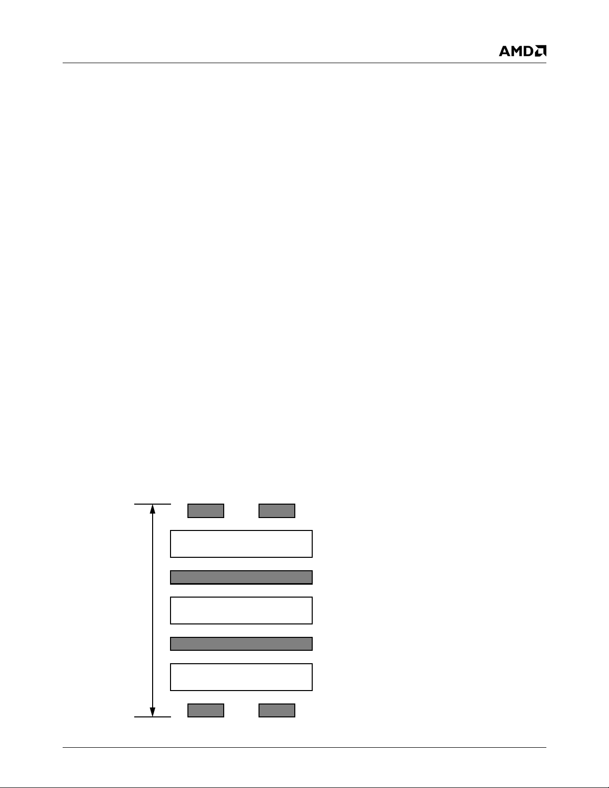
Figure 3-1 details a typical stackup for a four-layer PCB
which is suitable for a PC-133 system design with the GX1.
Many board shops do not prefer to have the designer “ov erspecify” the stackup requirements. Therefore, the main elements to specify include:
Minimum Line Width: 5 MILs
Nominal Trace Impedance: 63 Ω ±10% (at 5 MILs)
Minimum Dielectric Thickness: 5 MILs
Overall Board Thickness: 60.5 MILs ±3 MILs
{Note: 1 MIL = 0.001 inch = 0.0254 mm}
The key factor in determining the stackup for a PCB is
obtaining the correct trace impedance for memory signal s.
For best signal quality, match the output impedance of a
particular driver, when added to the impedance of the
series termination (if any), to the characteristic impedance
of its associated trace. The four factors directly affecting
trace impedance, in decreasing order of significance, are:
1) Dielectric height above the reference plane (in MILs).
2) The trace th ickness (in oz. of Cu).
3) Trace width (in MILs).
4) The dielectric constant of the material.
Of these four factors, the height above the reference plane,
the trace thickness and the dielectric constant are fixed by
the stackup. See Section 3.3 "Default Impedance, Trace
Widths and Spacing" on page 4 for details on recommended trace widths and spacing.
For purposes of reducing crosstalk, the minimum trace-totrace spacing should influence the necessary dielectric
height of a signal layer above its referenced plane. For
proper return current and minimal crosstalk, it is recommended that the ideal specified dielectric height of the
stackup be no more than half the trace spacing. In no case
should the dielectric height be more than the trace-to-trace
spacing, since the coupling between traces is stronger than
between a single trace and its reference plane. For typical
5-5 routing (5 MIL traces - 5 MIL spaces), this points to an
ideal dielectric height of about 2.5 MILs in order to significantly reduce the potential for crosstalk. Howev er, this does
not take into account the characteristic trace impedance
constraints. Also, the actual dielectric height is constrained
by the most cost effective prepreg process and by manufacturability issues, giving a minimum manufacturable
dielectric height of about 4 MILs. In order to achieve the
desired impedance, as well as to specify a manufacturable
PCB, this recommendation specifies a dielectric height of 5
MILs, giving a 1:1 ratio of trace spacing to dielectric height.
To mitigate the potential for crosstalk, separate parallel
traces by 2H spacing at least once ever y 1.5-2.0 inches of
parallel 1H trace routing. (See Section A.3 "Definitions" on
page 26 for “2H spacing” definition.) For synchronous signals on the same bus, 1H spacing is acceptable, since
each signal settles (has a setup period) before being
clocked at the load. Spacing between a clock and a synchronous bus should be 2H.
Top of PCB
~60.5 MILs
Bottom of PCB
Dielectric
Dielectric
Dielectric
ε
r
ε
r
ε
r
= 4.2
= 4.2
= 4.2
0.5 oz. Cu plated to 1.0 oz. 63Ω @ 5 MIL, 56Ω @ 6.5 MIL
54Ω @ 7 MIL
5.0 MILs
1.0 oz. Cu GND plane
~45 MILs
1.0 oz. Cu PWR plane
5.0 MILs
0.5 oz. Cu plated to 1.0 oz. 63Ω @ 5 MIL, 56Ω @ 6.5 MIL
54Ω @ 7 MIL
Figure 3-1. Typical GX1 Four-Layer Stackup
AMD Geode™ GX1 Processor PC133 Layout Recommendations 3
Page 4

Application Note
Revision 3.0 - June 2001 - Confidential
Once the dielectric height has been determined, specify
the spacing between the two power/ground planes to give
the desired overall board thickness. Actual power/ground
plane spacing is based upon availability of standard FR-4
cores. This recommendation specifies a core thickness of
45 MILs, giving an overall board thickness of approximately
60.5 MILs.
Dielectric height, thickness of copper and dielectric con-
stant are usually calculated for the maximum required
impedance, when at the minimum trace width and spacing.
For example, a target impedance of 63Ω with 5-5 traces
should dictate the dielectric height, thickness of copper and
dielectric constant. Other signal types may then use wider
traces for reduced impedance, given that the dielectric
height, thickness of copper and dielectric constant have
already been fixed. This recommendation specifies a trace
thickness of 0.5 oz. of copper, plated up to 1.0 oz. total on
the signal layers. Inner layer planes a re also specified at
1.0 oz. of copper. (Taller traces more closely approximate
cylindrical traces, which have significantly more inductance.) The default dielectric constant should target ε
4.2. Unfortunately, actual manufacturing processes are not
always able to so tightly control these parameters. Ideally, a
board designer works with the board shop to adjust the
available materials and processes in order to achieve the
specified impedance, which is the most important factor in
determining the end stackup arrangement. In the end, tight
control of signal impedance with the smallest tolerance for
error is the most important parameter for a successful
PC133 layout using the GX1 processor.
r
=
ing recommendations, some designers may wish to
increase impedance values on interfaces which are not
required to directly escape from the GX1 by specifying a
minimum trace width of 4 MILs for the PCB rather than 5
MILs. Again, working with the board shop to achieve an
optimal balance of signal integrity wi th volume manufacturability should dictate actual stackup, width and spacing
specifications.
3.4 Power and Ground Traces
• Trace Width: 25 MILs
• Trace Spacing: 5 MILs minimum
• Maximum trace length to via: 50 MILs
• Routing Bypass Capacitors (see Figure 3-2):
Connect capacitors directly to planes. Do not escape
directly from a EBGA or SPGA land pad to the pad of the
capacitor, finally escaping beyond the capacitor to a via.
Instead, escape the land pad directly to a close-by via
using a 25 MIL trace. Then, separately, escape from the
pad of the capacitor to its own via. Do this for both PWR
and GND connections. Place the decoupling capacitor
within 50 MILs of its associated PWR/GND land pads
where possible. Place capacitor escape vias as close to
each other as possible to reduce loop inductance. The
ideal via spacing may not always be achievable for smaller
footprint parts (i.e., 0603 capacitors).
Additional notes on decoupling:
3.3 Default Impedance, Trace Widths
and Spacing
The default trace width and spacing for the memory interface of the GX1 is 5-5. Using 5 MIL traces and 5 MIL spacing, a 5 MIL dielectric height, 1.0 oz. planes a nd 0.5 oz. of
Cu plated to 1.0 oz. total for the signal layers gives a target
characteristic trace impedance of ~63Ω. When determining
spacing requirements, keep in mind that 1H spacing leads
to ~15% crosstalk for any signal longer than the critical
length (~2 inches for 2 ns rise time), whereas 2H spacing
only leads to ~4% crosstalk.
3.3.1 Recommended Stackup, Trace Width,
and Trace Spacing Limitations
The maximum achievable trace impedance is about 63Ω
for the recommended stackup and minimum trace width.
Escape routing constraints of the GX1’s EBGA package do
not allow two traces to fit between rows of land pads using
greater than 5-5 routing. If 20 MIL pads were to be defined
for the EBGA, then 6-6 routing could be used for EBGA
escapes, with stackup parameters adjusted to give ~63Ω of
impedance. Smaller trace widths could then be used to
achieve higher impedance values (5 MILs ~ 70Ω, 4 MILs ~
75Ω). However, given the default stackup, width and spac-
• Use 25 MIL etch between pad and via.
• For 3528 or larger SMT caps, use two vias per pad.
Routing Resistors:
• For direct connect to plane, use 25 MIL trace width with
minimum length to the via.
• For series termination resistors, place as close to the
driver as possible.
• For resistor packs connecting to either power or ground,
four connections may share a via if the resistor pack is
being used for a pull-up/-down, strap option or other DC
type signal. Use multiple vias for resistor packs that are
used for terminating individual signals.
4 AMD Geode™ GX1 Processor PC133 Layout Recommendations
Page 5
Application Note
Revision 3.0 - June 2001 - Confidential
3.5 Decoupling
The instantaneous switching current requirements of the
PC133 sub-system on the GX1 can be provided by the
decoupling capacitors close to the GX1 and SODIMM or
DIMM. Charge from the planes replenishes the device
capacitance, the high frequency capacitors replenish the
planes, bulk capacitance replenishes the high frequency
capacitors. The aggregate capacitance (interplane, bulk
and high frequency) must also provide a low impedance
AC path to ground for the power supplies. In general, four
to eight bulk decoupling capacitors, depending upon how
large the plane is, should be spread out over the memory
power plane (using ~22 µF). For high speed noise rejection
and an improved low impedance AC path to ground at
higher frequencies, place several smaller value capacitors
in parallel between the power rail being decoupled and its
associated ground. Place each high-speed bypass capacitor (using ~0.10 µF) as close to a power pin as possible in
order to supply the instantaneous switching currents
required by the PC133 memory subsystem (GX1 and
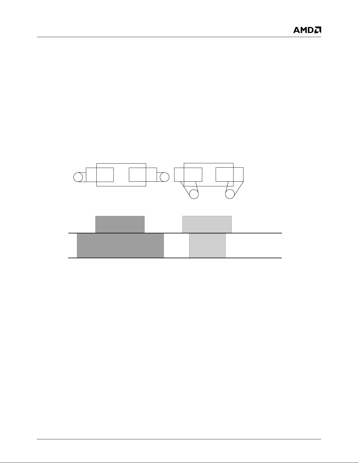
SODIMM or DIMM). Use the preferred capacitor placement/routing strategy detailed in Figure 3-2 for placement
and routing of the bypass capacitors.
poor
Capacitor
Large Loop Area:
Larger Inductance
good
Capacitor
Smaller
Loop Area
Figure 3-2. Decoupling Capacitors Pad Escaping
Signal Layer
Ground Plane
AMD Geode™ GX1 Processor PC133 Layout Recommendations 5
Page 6

4.0 SDRAM Interface
The PC133 SDRAM interface is a crucial high-speed digital
interface. Proper termination, minimal trace length and
some amount of trace length matching can all help contribute to a successful SDRAM interface layout. Haphazard
layout techniques can lead to poor signal quality due to
reflections, insufficient rise/fall times, or too much clock
skew at the SODIMM or DIMM. When escaping the
SDRAM interface, attempt to minimize the trace length to
the series termination. Place the SODIMM or DIMM as
close as possible to the termination. Attempt to route the
entire SDRAM interface such that each trace length is
within ~300 ps (~2 inches) of the nominal value. Keep the
entire SDRAM interface as short as possible and no
greater than 5 inches when connected to SODIMMs. For a
333/111 MHz design, the SDRAM interface to the SODIMM
is further reduced to 3.5 inches. For best operation, attempt
to route most of the SDRAM interface over a solid ground
plane rather than a solid power plane. For this recommendation, this implies routing on the top layer only, where feasible. The SDRAM interface flows off of the GX1 with good
correlation to pin ordering on the SODIMM or DIMM, simplifying the routing of this interface. If too many vias are
clustered in one area, try to spread the traces out. In the
EBGA version, attempt to route the outer three rows on the
top layer without using vias, since minimizing vias and lay er
transitions improves signal quality.
In PC133 signal groups, there are two groups.
• 1T (7.5 ns) Signals:
— MD, DQM, CS, CKE
• 2T (15 ns) Signals:
— MA, RAS, CAS, WE
• Loads (1-2 SODIMM or 1 DIMM):
— Address/Command: max = 16; min = 4
— CLK: max = 4; min = 4
— CS: max = 4; min = 4
— CKE: max = 8; min = 4
— DQ/DQM: max = 4; min = 1
• Serial termination resistor:
— Use a 10Ω resistor or serial termination on all signals
between the GX1 and the memory device.
Application Note
Revision 3.0 - June 2001 - Confidential
4.1 Clock Routing
SODIMM
• SDRAM Clocks (SDCLK[3:0]):
— Trace Width: 6 or 7 MILs to source termination (58Ω
or 54Ω), 7 MILs from termination to receiver (Target
impedance: 54Ω).
— Minimum Trace Spacing (within the group): 9 MILs to
source termination, 16 MILs from termination to
receiver.
— Minimum Trace Spacing (to other groups): 9 MILs to
source termination, 16 MILs from termination to
receiver.
DIMM
• SDRAM Clocks (SDCLK[3:0]):
— Trace Width: 5 MILs to source termination (63Ω),
5 MILs from termination to receiver (Target impedance: 63Ω).
— Minimum Trace Spacing (within the group): 9 MILs to
source termination, 16 MILs from termination to
receiver.
— Minimum Trace Spacing (to other groups): 9 MILs to
source termination, 16 MILs from termination to
receiver.
— The SDCLK[3:0] signals from the CPU must be
routed to pins 42, 79, 125, 163 of the DIMM, respectively. This makes each clock have four loads per
clock line.
6 AMD Geode™ GX1 Processor PC133 Layout Recommendations
Page 7

Application Note
Revision 3.0 - June 2001 - Confidential
The most critical components of the SDRAM interface are
the clocks. The GX1 outputs four SDRAM clocks that must
be routed to the SODIMM or DIMM. Use no more than two
vias per clock trace from driver to source. This includes the
SDCLK_OUT to SDCLK_IN delay loop. Match SDRAM
clock traces to each other within ±250 MILs in length. This
matching includes both the length to the termination and
the length from the termination to the SODIMM or DIMM.
For SDCLK looping, maintain a 16 MIL spacing requirement between each clock trace, including itself. The default
trace width/spacing is different for the land pad-to-termination segment than for the remaining segment from the termination to the SODIMM or DIMM. The reason for this is to
help facilitate land pad escaping from the SPGA or the fine
pitch EBGA. A 6 MIL trace with 9 MIL spacing requirements allows one clock trace escape between land pads,
thereby reducing the chance of coupling with other traces.
Listed below are key design issues when routing the
SDCLKs:
• Minimize the use of vias along the clock traces. No vias
is best, two vias maximum.
• Route the clock trace entirely on the top layer if possible,
thereby referencing the ground plane below it.
• Maintain 16 MIL spacing from all other signals, including
itself when routing clock loops.
• Route clocks with a maximum of ±250 MILs trace length
mismatch.
• Place the series termination as close to the GX1 as
possible.
• Place the SODIMM or DIMM as close to the termination
as possible.
4.1.1 SDRAM Clock Consideration
The SDRAM clocks generated by the GX1 are not perfectly
periodic; some clock periods can be slightly longer and others slightly shorter. The percentage of this difference is
around 12%. For example, at 100 MHz SDCLK (300 MHz/3
divide) the frequency of this is approximately 110 to 90
MHz. This jitter is the reason for requiring PC133 memor y
for speeds of 90 MHz and higher
4.1.2 SDCLK_OUT to SDCLK_IN
The SDRAM interface also includes a SDCLK_OUT to
SDCLK_IN clock topology that is used for properly timing
read cycles. The ideal length for this trace is the same as
the overall length of the SDCLK outputs to the load (the
memory on the SODIMM or DIMM, not the connector
itself). Additional delay loops are usually included in order
to optimize cycle setup/hold times, and may be used by
populating stuff option resistors to give either no delay, 0.5
ns of dela, or 1.0 ns of delay total.
Delay is also programmable in software by modifying shift
clock values in the MC_MEMC_CNTRL2 (GX_BASE+
Memory Offset 8404h) register. Adding the delay loops to
the board provides the most flexibility in maximizing the
timing margin.
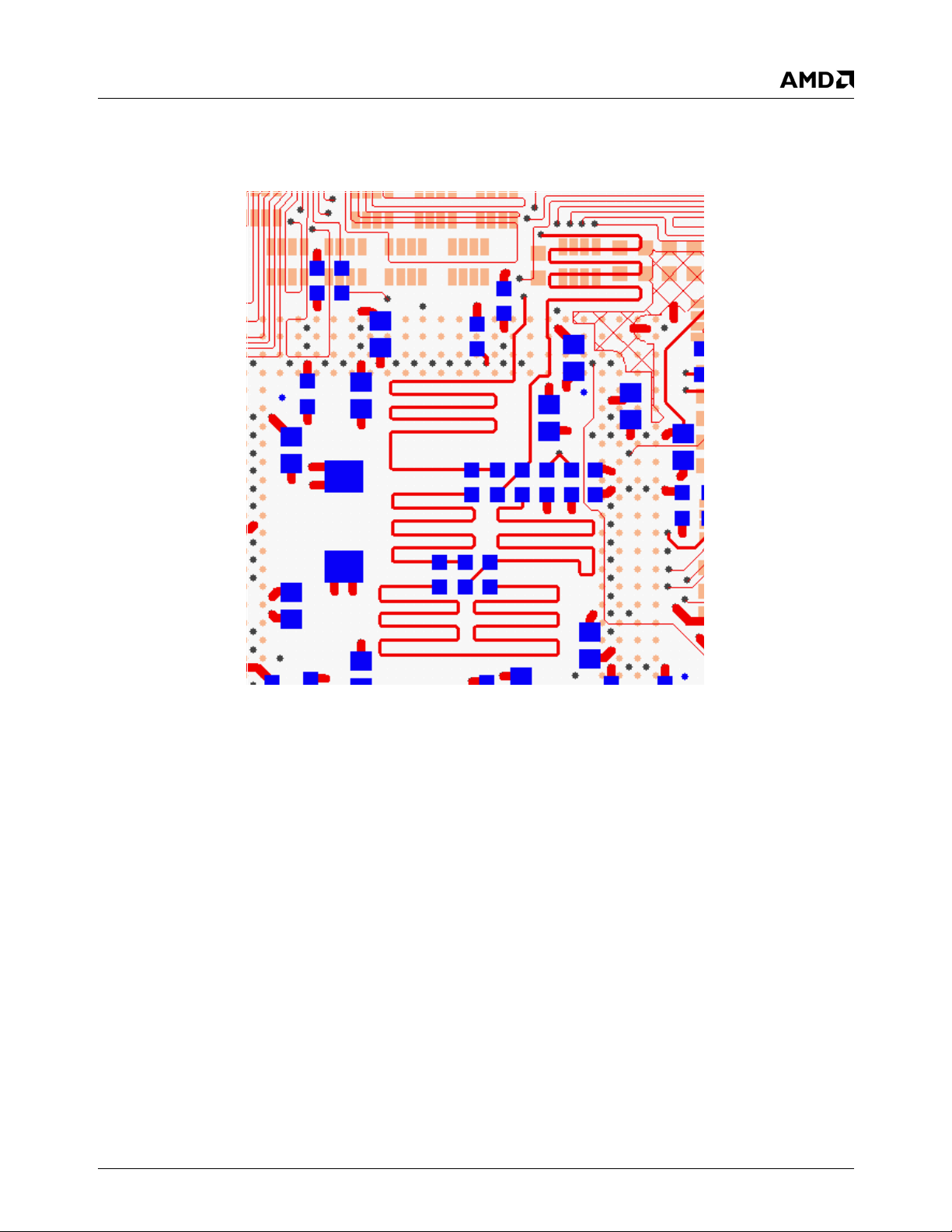
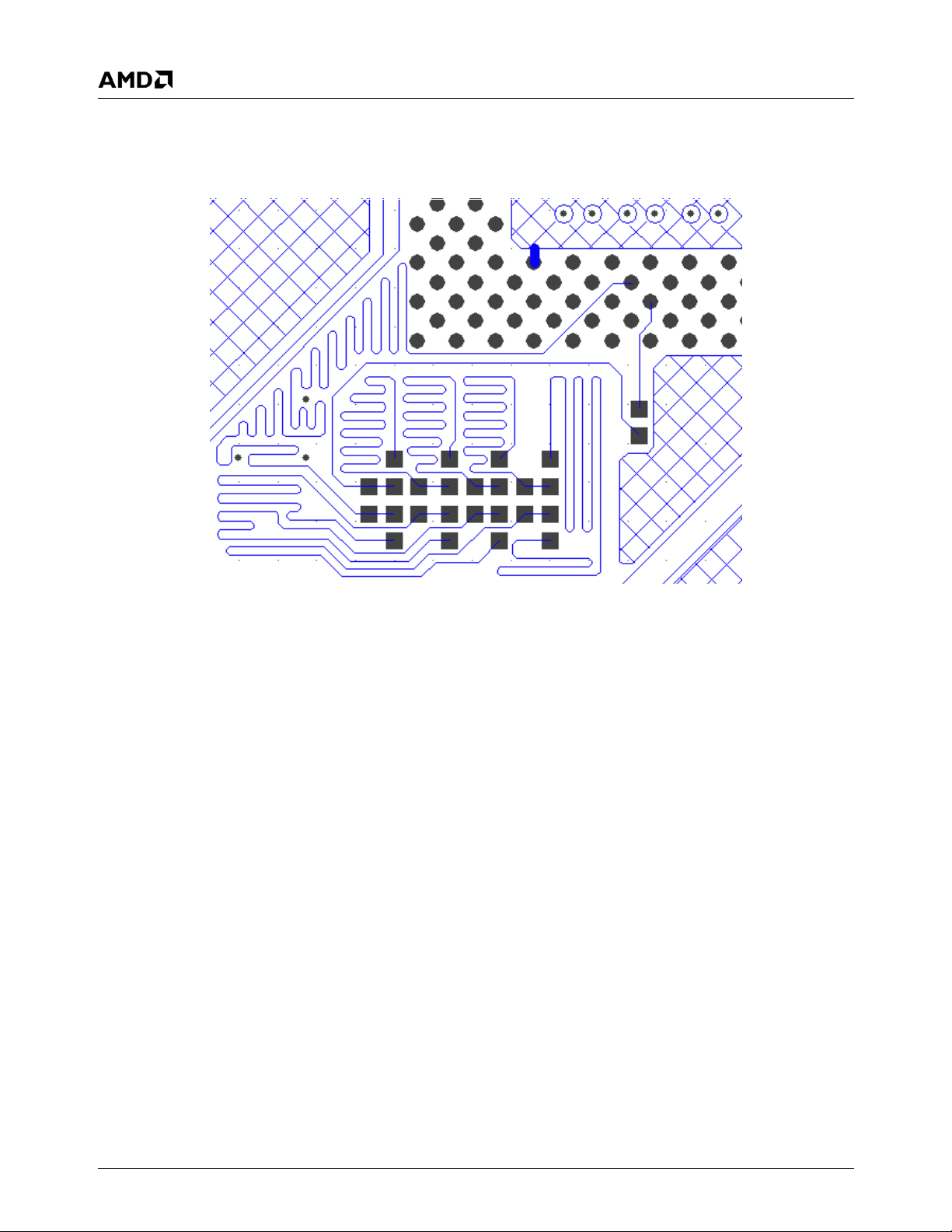
To route the SDCLK_OUT to SDCLK_IN delay loop, use
one via (in EBGA) to immediately traverse to the bottom
layer upon escaping from SDCLK_OUT, then immediately
connect to the series terminating resistor. Beyond the
series termination, place all delay loop components and
trace loops on the bottom side of the PCB, keeping at least
16 MILs of separation between the loop and all other traces
including itself. Use one final via (in EBGA) to traverse bac k
up to the top layer and connect with SDCLK_IN. Match the
main loop’s length to that of the SDCLK[0/1/2/3] clock, plus
an additional 3.0 inches if using DIMMs or 2.5 inches for
SODIMMs to account for the added trace distance to the
memory ICs on the SODIMM or DIMM.
Note: Standard DIMMs route the clock an additional 3.10
inches from the edge connector on the DIMM to
the loads. For SODIMMs, the clock is routed 2.50
inches ±0.05 inches from the edge connector to
the memory chips.}
The first loop may need adjusting after the rest of the
SDRAM interface is routed, so leave some extra room for
additional loop area. Once the first loop is routed, route two
additional delay loops of 0.5 ns each (~3.5 inches) using
resistor stuff options to select the appropriate delay loop.
To summarize, the required delay loops are as follows:
• LOOP1 (MILs) = [SDCLK0+ SDCLK1 + SDCLK2 +
SDCLK3] (MILs) / 4 + 2500 MILs (SODIMM), 3000 MILs
(DIMM), or 0 MILs (soldered down memory)
— Average of SDCLK distances plus SODIMM or DIMM
trace length.
• LOOP2 (inches) = LOOP3 (inches) = 3.5 inches
— 0.5 ns delay per 3.5 inch loop.
• LOOP1 + LOOP2 + LOOP3 = 0 ns + 0.5 ns +
0.5 ns = 1 ns
— Total delay available to GX1 when all loops are used.
Also, one decoupling capacitor in the immediate area
where each SDCLK[x] trace traverses a via to the opposite
side of the PCB can help provide a local return current path
without adding unnecessary loop inductance or stray currents. If guard traces are used during routing of the
SDRAM clock lines, they may either be removed once the
remainder of the interface has been routed, or be stitched
to digital ground at intervals of approximately one via every
500 MILs.
AMD Geode™ GX1 Processor PC133 Layout Recommendations 7
Page 8

4.2 SDRAM Controls, Data and Address
The target characteristic impedance of the entire SDRAM
interface is 55Ω, ±10% (SODIMM) or approximately 60Ω to
80Ω (DIMM). Keep data lines DATA[63:0] separate from
control lines. The control lines for the SDRAM interface are
as follows: CKE[1:0], CS[3:0]#, RAS[1:0]#, CAS[1:0]#,
WE[1:0]#, MA[12:0], DQM[7:0]. Attempt to route the entire
SDRAM interface such that each trace length is within
±300 MILs of nominal value.
Note that two different default width/spacing recommendations are made for each subsection of the SDRAM interface. The reason for this is to more closely match the target
55Ω impedance of the SODIMM traces or approximate
60Ω to 80Ω of the DIMM, beyond the termination, while
simultaneously accepting the limitation of escaping the
EBGA or SPGA with narrower traces. The second
width/spacing recommendation more closely matches the
correct impedance for the interface.
4.2.1 SODIMM
• Control lines (CKE[1:0], CS[3:0]#, RAS[1:0]#,
CAS[1:0]#, WE[1:0]#, MA[12:0], MTEST[3:0] and
DQM[7:0]):
— Trace Width: 5 MILs to source termination (63Ω),
6.5 MILs from termination to receiver (Target impedance: 55Ω)
— Minimum Trace Spacing (within the group): 5 MILs to
source termination, 6.5 MILs from termination to
receiver
— Minimum Trace Spacing (to other groups): 5 MILs to
source termination, 10 MILs from termination to
receiver
• Data Lines (DATA[63:0]):
— Trace Width: 5 MILs to source termination (63Ω),
6.5 MILs from termination to receiver (Target impedance: 55Ω)
— Minimum Trace Spacing (within the group): 5 MILs to
source termination, 6.5 MILs from termination to
receiver
— Minimum T r ace Spacing (to other groups): 10 MILs to
source termination, 10 MILs from termination to
receiver
Application Note
Revision 3.0 - June 2001 - Confidential
4.2.2 DIMM
• Control lines (CKE[1:0], CS[3:0]#, RAS[1:0]#,
CAS[1:0]#, WE[1:0]#, MA[12:0], MTEST[3:0] and
DQM[7:0]):
— Trace Width: 5 MILs to source termination (63Ω),
5 MILs from termination to receiver (Target impedance: 63Ω)
— Minimum Trace Spacing (within the group): 5 MILs to
source termination, 6.5 MILs from termination to
receiver
— Minimum T r ace Spacing (to other groups): 10 MILs to
source termination, 10 MILs from termination to
receiver
• Data Lines (DATA[63:0]):
— Trace Width: 5 MILs to source termination (63Ω),
5 MILs from termination to receiver (Target impedance: 63Ω)
— Minimum Trace Spacing (within the group): 5 MILs to
source termination, 6.5 MILs from termination to
receiver
— Minimum T r ace Spacing (to other groups): 10 MILs to
source termination, 10 MILs from termination to
receiver
8 AMD Geode™ GX1 Processor PC133 Layout Recommendations
Page 9
Application Note
Revision 3.0 - June 2001 - Confidential
5.0 Placement, Ball Escaping, Via Size and Routing Order
5.1 Placement
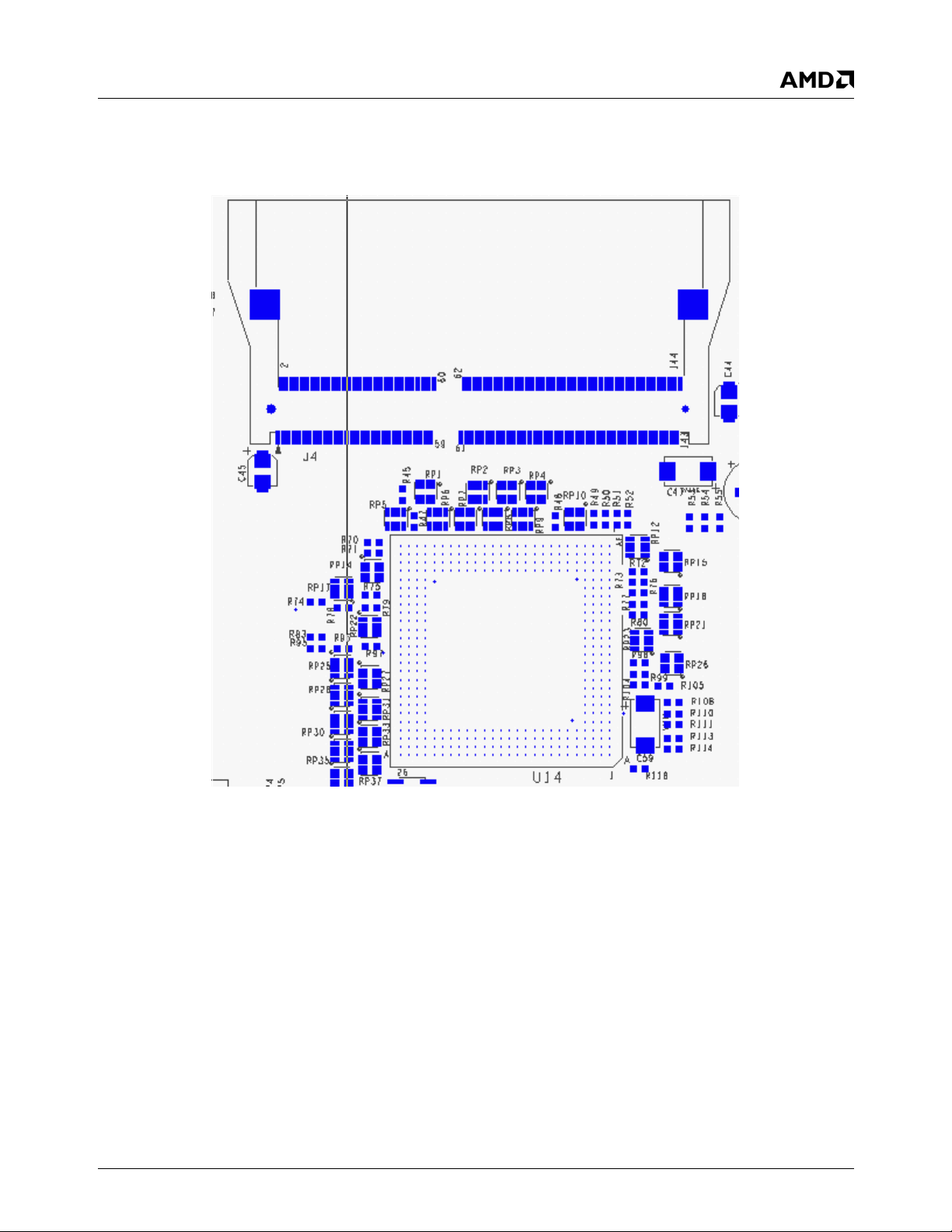
Always place the SODIMM as close to the AN37 or AF26
corner as possible. It is preferred that the land pads for the
EBGA be defined as 25.0 MIL circular copper pads. This
generally results in slightly more manufacturing deviation
than when SMD (solder mask defined) pads are used, but
SMD pads must be oversized at ~30 MILs of actual copper,
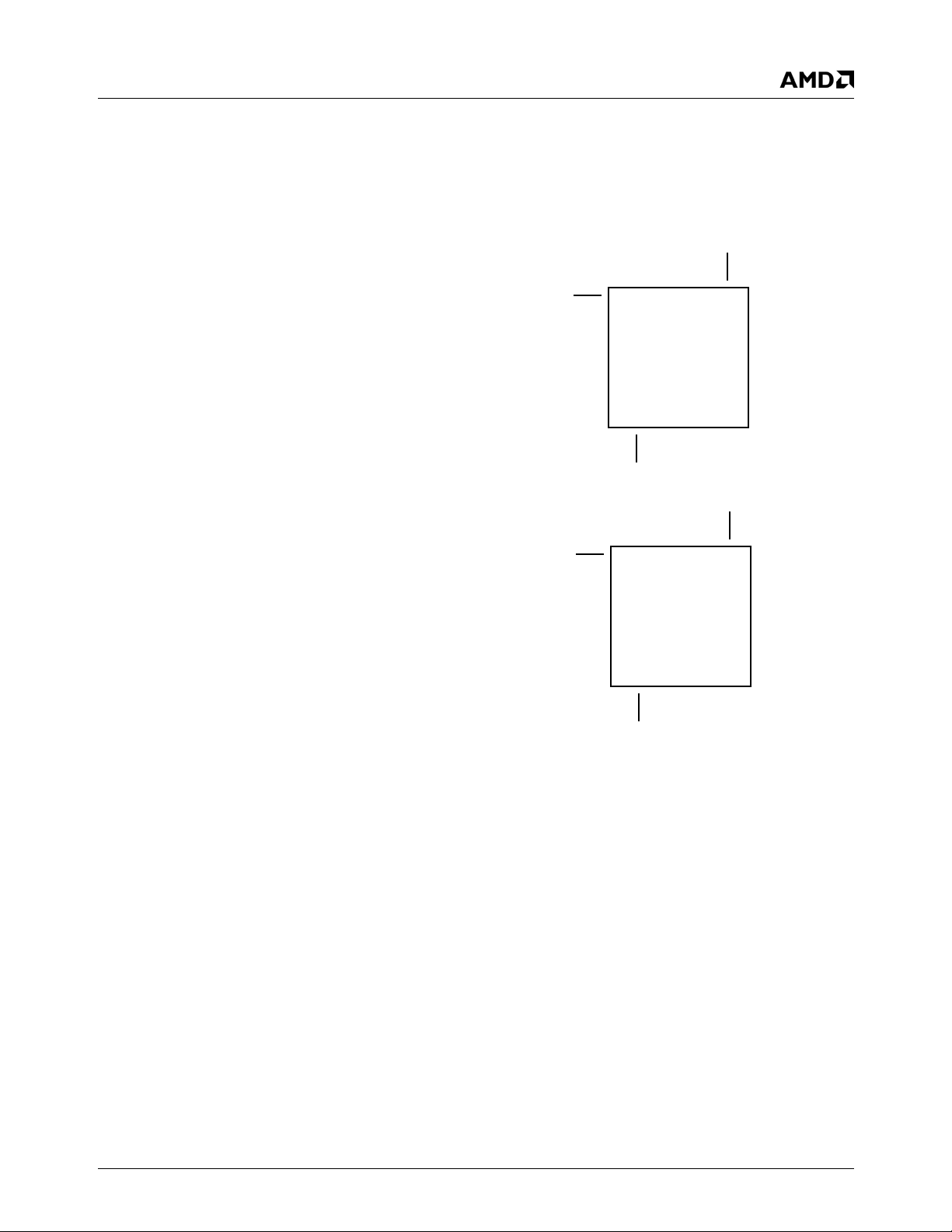
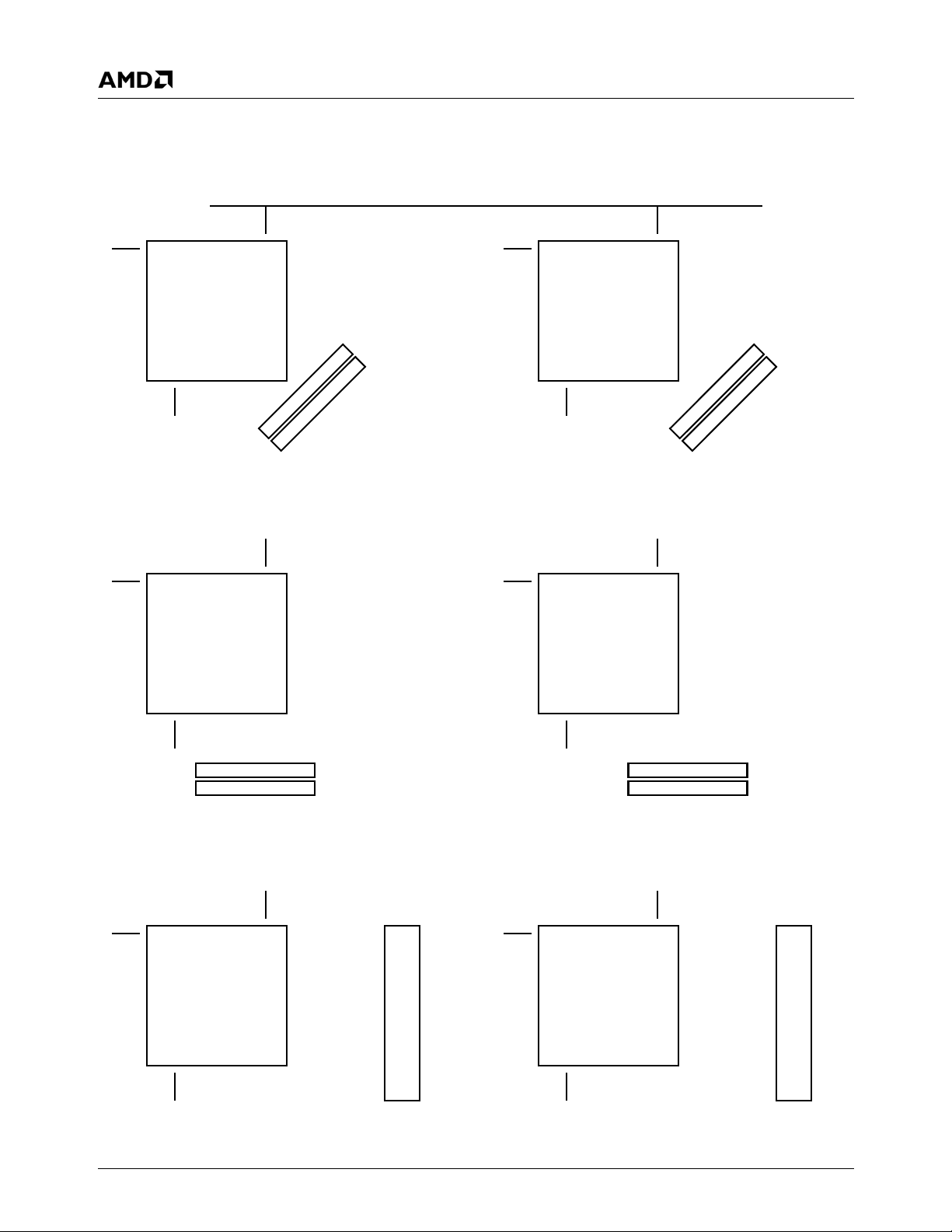
which cuts down on routing channels. Figures 5-1 through
5-4 illustrate recommended component placement configurations.
Graphics IF
PCI
A1
AMD Geode™ GX1
Processor (SPGA)
AN1 AN37
Memory IF
PCI
A37
Memory IF
A26
Memory IF
Memory IF
Graphics IF
A1
AMD Geode™ GX1
Processor (EBGA)
AF1 AF26
Figure 5-1. Recommended Component
Placement: Top View - Both PCB and SI
AMD Geode™ GX1 Processor PC133 Layout Recommendations 9
Page 10
Application Note
Revision 3.0 - June 2001 - Confidential
PCI
Graphics IF
A1
AMD Geode™ GX1
Processor (SPGA)
AN1 AN37
PCI
Graphics IF
A1
AMD Geode™ GX1
Processor (SPGA)
PCI
A37
Graphics IF
A1
Memory IF
AMD Geode™ GX1
Processor (EBGA)
AF1 AF26
Memory IF
Memory IF
SODIMM 0 & 1
Figure 5-2. Recommended SODIMM Placement: Top View - PCB
PCI
A37
Memory IF
Graphics IF
A1
AMD Geode™ GX1
Processor (EBGA)
A26
Memory IF
SODIMM 0 & 1
A26
Memory IF
AN1 AN37
PCI
Graphics IF
A1
AMD Geode™ GX1
Processor (SPGA)
AN1 AN37
AF1 AF26
Memory IF
Memory IF
SODIMM 0
SODIMM 1
Figure 5-3. Recommended SODIMM Placement: Top View - PCB
PCI
A37
Memory IF
Memory IF
DIMM DIMM
Graphics IF
A1
AMD Geode™ GX1
Processor (EBGA)
AF1 AF26
Memory IF
SODIMM 0
SODIMM 1
A26
Memory IF
Figure 5-4. Recommended DIMM Placement: Top View - PCB
10 AMD Geode™ GX1 Processor PC133 Layout Recommendations
Page 11
Application Note
Revision 3.0 - June 2001 - Confidential
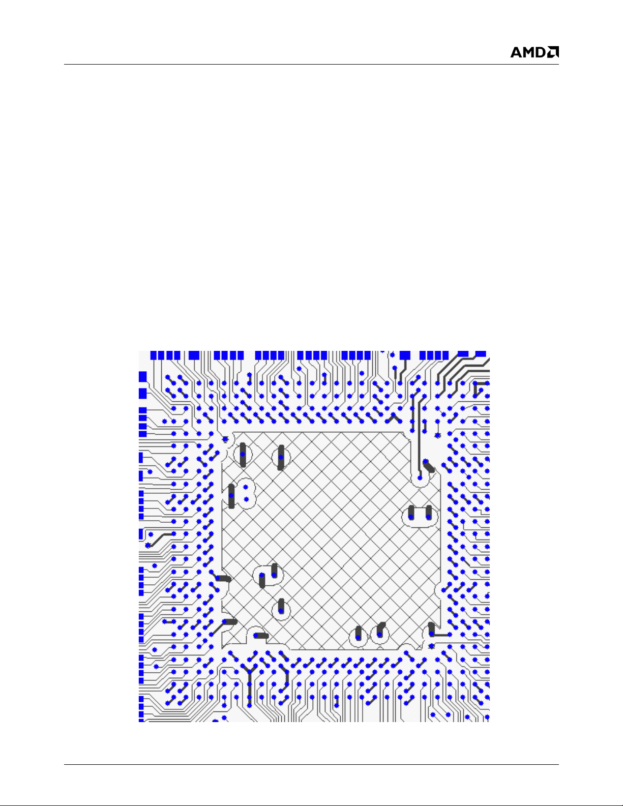
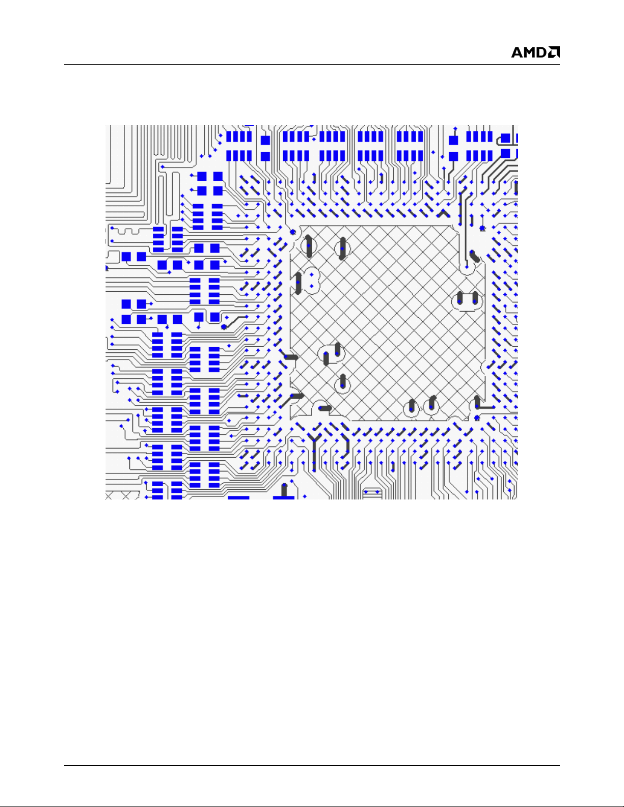
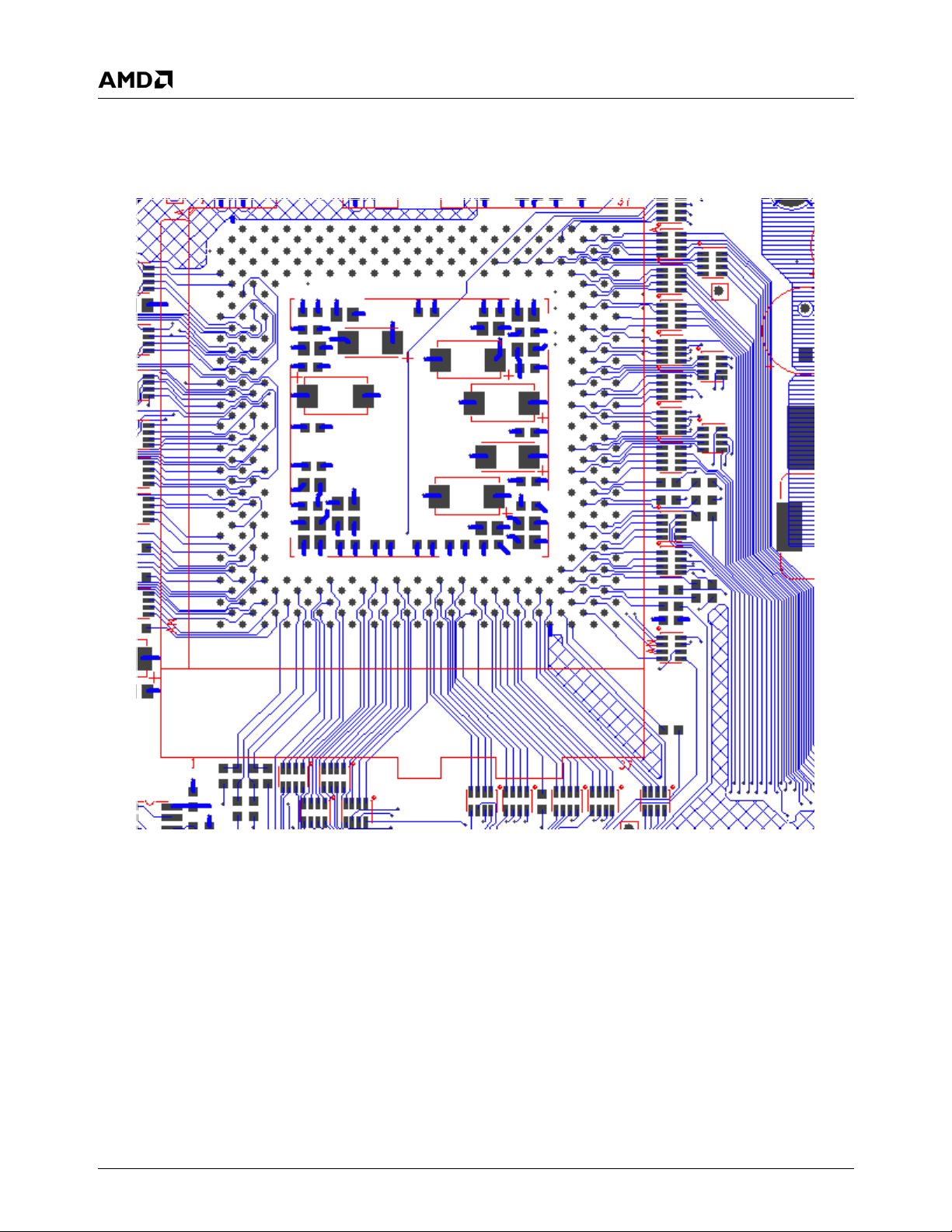
5.2 Pin or Ball Escaping of Memory Interface Signals
A via fits between any set of four land pads of the EBGA,
as shown in Figure 5-5. Since the land pads are defined
only on the top layer, it is necessar y for some signals to
trace-escape from the land pads to a via, then continue
routing the trace on the bottom layer away from the EBGA.
Using 5 MIL traces to escape the EBGA, allows two traces
to fit between land pads. Therefore, the outer three rows of
land pads should always be escaped on the top layer only.
Exceptions occur when vias block the top layer routing
channel, as in the case of power and ground traces which
must escape the land pad, then connect through a via to
their respective planes. In this case, the third row land pads
(from the outside of the part, not the actual row number)
also must be escaped to a via first, then routed on the bottom layer away from the EBGA. Avoid areas of high density
via population, as this can choke current paths. Following
are some specific recommendations pertaining to th e ball
escaping of the GX1:
• Route the escape traces for adjacent power/ground land
pads in opposite directions to increase routing channels.
Route these traces inward, placing the via toward the
cavity so that the second row land pads may still be
escaped on the top layer. (See Figure 5-5.)
• When escaping a signal (not power or ground) from a
land pad, attempt to place the via away from the cavity
of the part, then continue routing away from the EBGA.
To increase routing channels, however, some vias may
need to be staggered. In other words, escape every
other trace inward (toward the cavity) and the remaining
traces outward (awa y from the cavity) to their associated
vias when necessary.
• For clock signals which stay on the top layer, attempt to
route them without sharing a routing channel (between
land pads) with any other signals.
• Escape each power/ground land pad to only one via.
(Try not to share vias.)
Figure 5-5. EBGA Ball Escaping
AMD Geode™ GX1 Processor PC133 Layout Recommendations 11
Page 12
Application Note
Revision 3.0 - June 2001 - Confidential
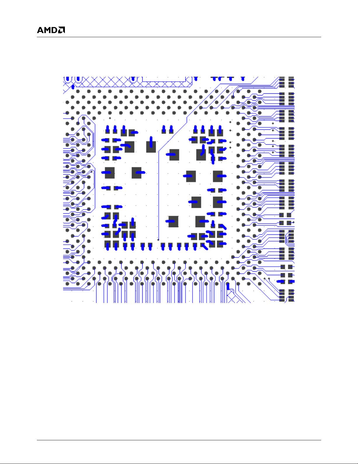
Figure 5-6. SPGA Pin Escaping
12 AMD Geode™ GX1 Processor PC133 Layout Recommendations
Page 13

Application Note
Revision 3.0 - June 2001 - Confidential
5.3 Default Vias
Modern PCB construction techniques dictate which vias
can be used most cost effectively. The smallest via size is
not obtained by a mechanical drill, but rather by laser drilling. However, this process is expensive and time consuming. For mechanically drilled vias, there is a limit of about
10 MILs on how small the diameter can be. Also, smaller bit
sizes break more easily and fewer layers can be simultaneously drilled due to bit wander. For most designs, the
depth of the via hole should never be more than six times
that of its diameter, although the actual manufacturable
aspect ratio depends upon the fabrication house. For a 60
MIL overall thickness PCB, this limits the smallest via to a
10 MIL drill. The most cost-effective PCB specification ideally uses a standard, larger bit size, and also uses the
same drill size for all vias on the PCB.
A PCB design that uses the Geode GX1 should take into
account the foregoing information. However, due to the
pitch of the EBGA package, standard large size drills do
not fit interstitially between land pads without compromising the via’s pad size, thereby leading to potential breakout.
This recommendation specifies a via size which is smaller
in order to accommodate the EBGA escape requirement,
yet still maintains manufacturability. Specifically, a plated
through hole, 12 MIL drill plated to 10 MIL inner diameter,
25 MIL pad, 35 MIL anti-pad and no default thermal connections via should be defined in the layout database (if it
does not already exist). The 25 MIL pad exactly fits in the
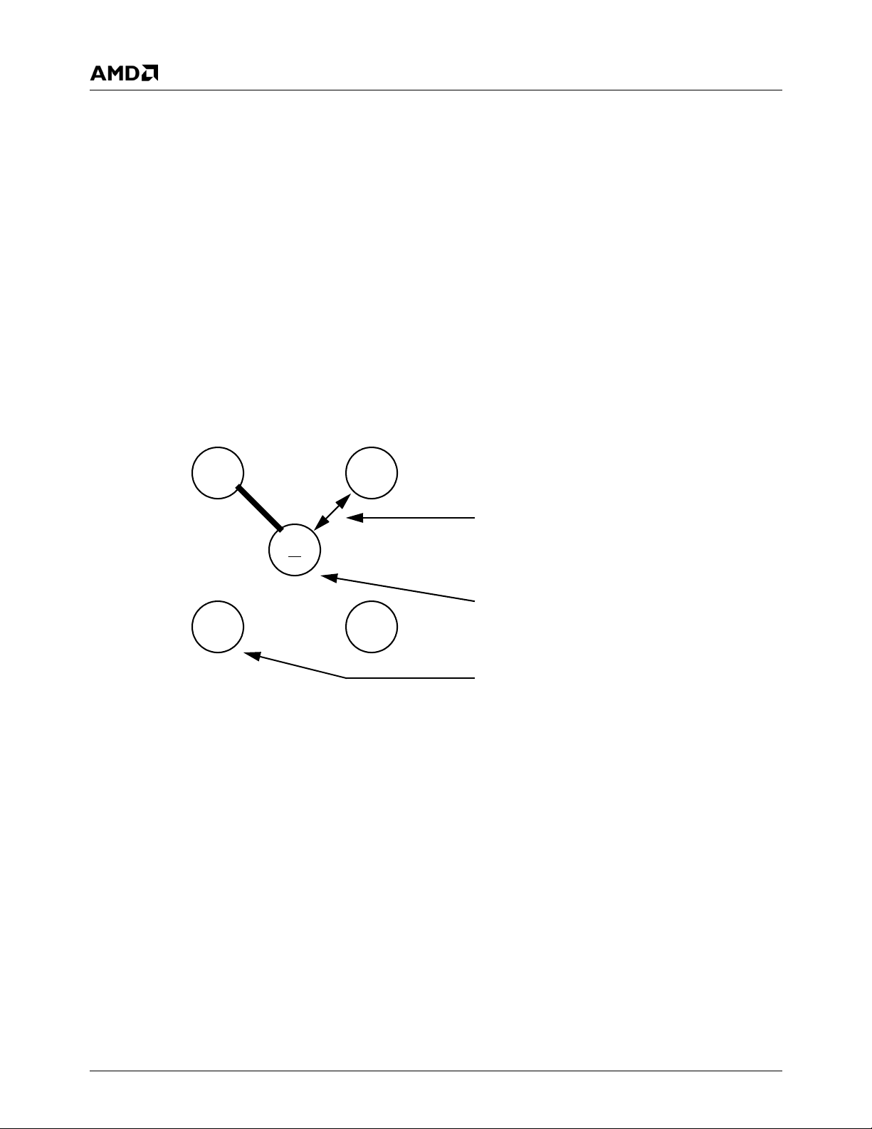
middle of any four land pads of the EBGA, while still maintaining a via-to-pad spacing constraint of 10 MILs minimum. See Figure 5-7 for an example of interstitial via
placement within the land pad pattern of the EBGA. For
maximum cost effectiveness, use the same via size
throughout the entire design. This increases routing channels as well as limits the effects of current choking in areas
of high density via population. In calculating the necessar y
neck width of the V
plane split, the size of the anti-pad
CORE
on the plane layer, use 35 MILs rather than the size of the
pad on the surface layer, 25 MILs.
AMD Geode™ GX1 Processor PC133 Layout Recommendations 13
Page 14
5.4 Routing Order
Once the GX1 has been placed, the steps listed next can
be used as a guide to proper routing order. Place the series
termination for the SDRAM clocks, then escape and route
the four SDCLKs to these resistors.
1) Place the SODIMM or DIMM connector and route the
SDRAM clocks from their termination to the connector.
Place guard traces on either side of the clocks to
maintain spacing constraints; these guard traces may
be removed after the rest of the SDRAM interface has
been routed if desired.
2) Place and route the clock delay loops for the SDRAM
interface. The first loop may need adjusting after the
rest of the SDRAM interface is routed, so leave some
extra room for additional loop area. The two outside
Ball
Ball
Application Note
Revision 3.0 - June 2001 - Confidential
loops are specified at fixed lengths of 3.6 inches (0.5
ns) each. See Section 4.0 "SDRAM Interface" on page
6.
3) Place all series termination resistors and resistor
packs for the SDRAM bus. Route the SPGA or EBGAto-termination interface.
4) Escape an d route over to join the rest of the SDRAM
bus signals.
5) Complete routing of the SDRAM interface from the termination resistors to the SODIMM or DIMM connector
side of the PCB.
EBGA Pitch: 50 MIL
Land Pad Air Gaps: 25 MIL
Trace
VI
Ball Ball
Default Air Gap: 10.36 MIL
(Via-to-Pad Spacing Constraint: 10 MIL)
12 MIL Drill, 25 MIL Pad
25 MIL Circular Land Pad
Figure 5-7. Interstitial Via Placement within EBGA Land Pattern
14 AMD Geode™ GX1 Processor PC133 Layout Recommendations
Page 15
Application Note
Revision 3.0 - June 2001 - Confidential
Appendix A Support Documentation
A.1 Impedance Calculations for All Target Impedances
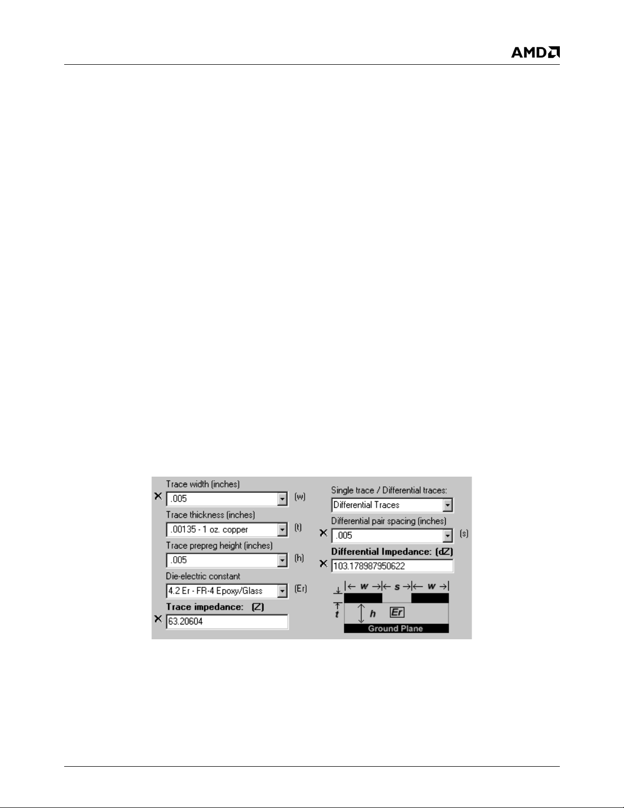
Figure A-1, Figure A-2, and Figure A-1 represent typical impedance calculations for all specified impedances used in the
design of a PCB using the Geode GX1. Formulas used were taken from “High-Speed Digital Design”, Johnson/Graha m,
Prentice Hall 1993, ISBN 0-13-395724-1, and are included here for reference.
Microstrip characteristic impedance, (0.1 < w/h ratio < 2.0):
Z
microstrip
Where:
Note that for w/h ratios over 2.0, this formula gives approximations which are increasingly lower than actual values. Earlier
in this document, default trace width-trace spacing requirements were given for PWR/GND signals. The impedance values
for these wide traces were calculated using the full impedance formula included in Appendix C of th e “High-Speed Digital
Design” text, rather than the above approximation which is only valid for w/h ratios of up to about 2.0.
(Ω) = (87 / SQRT(εr + 1.41)) * ln[5.98h / (0.8w + t)]
h is height above reference plane (inches),
w is trace width (inches),
t is line thickness (inches), and
is the relative permittivity of the substrate (dimensionless).
ε
r
Microstrip Propagation delay, (0.1 < w/h ratio < 2.0):
T
prop,microstrip
(ps/inch) = 85 * (SQRT(0.475εr + 0.67))
Note that this formula takes into account how the electric field splits between the substrate and air, reducing the effective
permittivity below the relative permittivity of the substrate. Use the permittivity of the substrate itself in this formula (i.e.,- ε
r
4.2.
Note that this value is not dependant upon trace or stackup geometry.
A typical value for propagation delay on a microstrip layer using εr = 4.2 is approximately 138 ps/in.
Figure A-1. Routing, 63Ω Impedance
=
AMD Geode™ GX1 Processor PC133 Layout Recommendations 15
Page 16
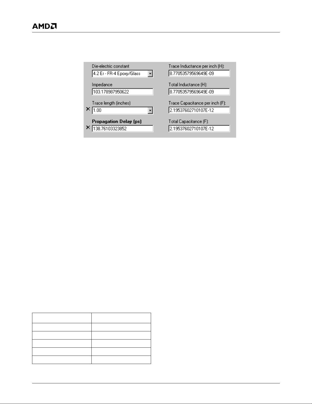
Figure A-2. 5-5 Routing, 138 ps Delay
Stripline characteristic impedance, (w/b ratio < 0.35 and t/b ratio < 0.25):
Z
microstrip1
Z
microstrip2
(Ω) = (60 / SQRT(εr)) * ln[1.9b / (0.8w + t)] (for h1 = h2)
(Ω) = 2 * (Z
microstrip1
[2*h1 + t] * Z
microstrip1
[2*h2 + t]) (for h1 ¼ h2)
-----------------------------------------------------------
Application Note
Revision 3.0 - June 2001 - Confidential
(Z
microstrip1
[2*h1 + t] + Z
microstrip1
[2*h2 + t])
Where:
b is separation between reference planes (inches),
h1 is separation between trace and upper reference plane,
h2 is separation between trace and lower reference plane, and
b = h1 + h2 + t.
Note that for w/b ratios over 0.35, this formula gives approximations which are increasingly lower than actual values.
Stripline propagation delay, (w/b ratio < 0.35 and t/b ratio < 0.25):
T
prop,microstrip
(ps/inch) = 85 * SQRT(εr)
Note that this value is not dependant upon trace / stackup geometry, nor does it depend on the per mi ttivity of air.
A typical value for propagation delay on a stripline layer using ε
= 4.2 is approximately 174 ps/in. In other words, signals
r
travel faster on outer layers (microstrip) than on inner layers (stripline).
Table A-1. Impedance Calculations
T race Width (MIL) Impedance (Ω)
5 63.2
6 58.1
6.5 55.8
7 53.6
9 46.0
16 AMD Geode™ GX1 Processor PC133 Layout Recommendations
Page 17
Application Note
Revision 3.0 - June 2001 - Confidential
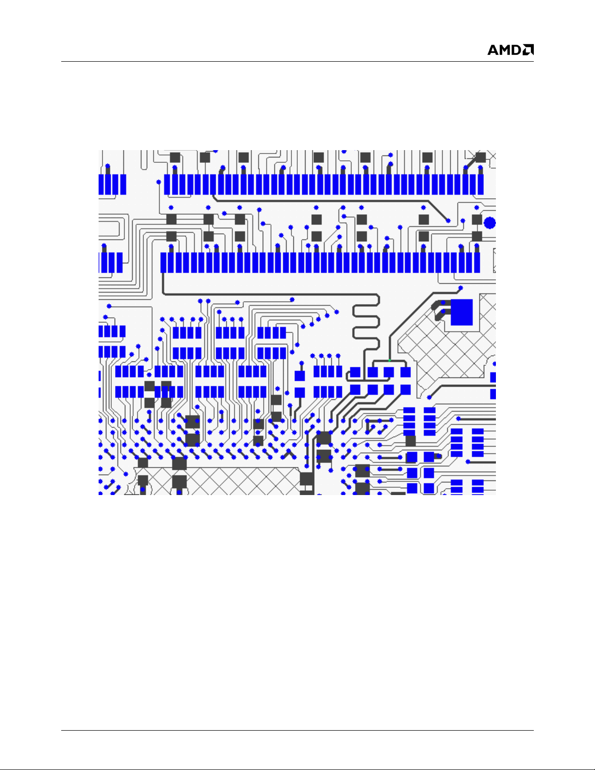
A.2 Sample Schematic Diagrams and Sample Layout Diagrams
Figure A-3. SDRAM Clocks in EBGA
AMD Geode™ GX1 Processor PC133 Layout Recommendations 17
Page 18
Application Note
Revision 3.0 - June 2001 - Confidential
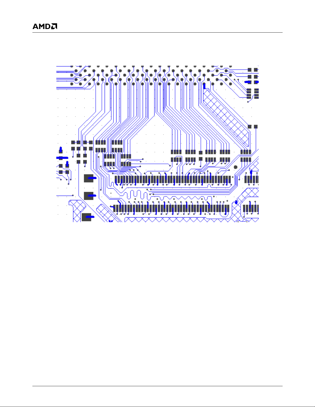
Figure A-4. SDRAM Clocks in SPGA
18 AMD Geode™ GX1 Processor PC133 Layout Recommendations
Page 19
Application Note
Revision 3.0 - June 2001 - Confidential
Figure A-5. SDRAMOUT-to-SDRAMIN Clock Delay Loops in EBGA
AMD Geode™ GX1 Processor PC133 Layout Recommendations 19
Page 20
Application Note
Revision 3.0 - June 2001 - Confidential
Figure A-6. SDRAMOUT-to-SDRAMIN Clock Delay Loops in SPGA
20 AMD Geode™ GX1 Processor PC133 Layout Recommendations
Page 21
Application Note
Revision 3.0 - June 2001 - Confidential
Figure A-7. SDRAM Escape to Series Termination in EBGA
AMD Geode™ GX1 Processor PC133 Layout Recommendations 21
Page 22
Application Note
Revision 3.0 - June 2001 - Confidential
Figure A-8. SDRAM Escape to Series Termination in SPGA
22 AMD Geode™ GX1 Processor PC133 Layout Recommendations
Page 23
Application Note
Revision 3.0 - June 2001 - Confidential
Figure A-9. Placement of SODIMM with EBGA
AMD Geode™ GX1 Processor PC133 Layout Recommendations 23
Page 24
Application Note
Revision 3.0 - June 2001 - Confidential
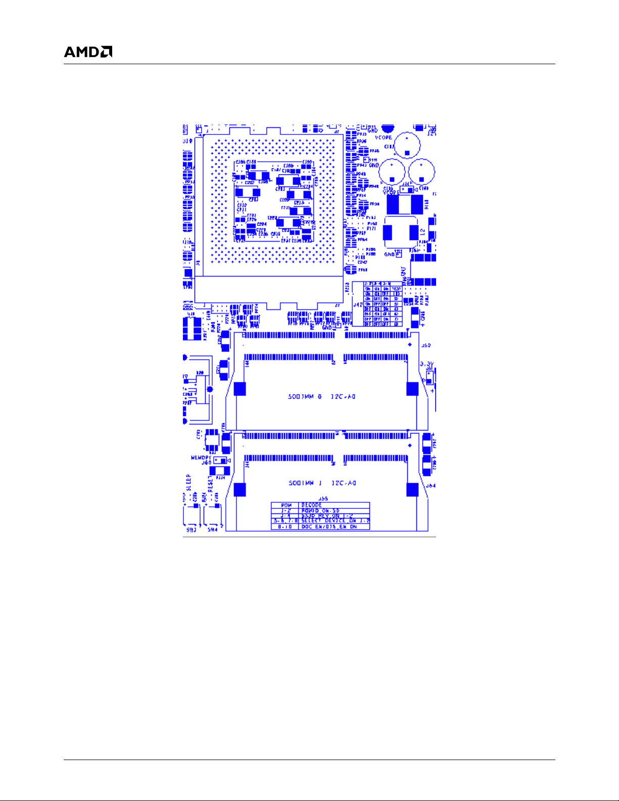
Figure A-10. Placement of SODIMMs with SPGA
24 AMD Geode™ GX1 Processor PC133 Layout Recommendations
Page 25
Application Note
Revision 3.0 - June 2001 - Confidential
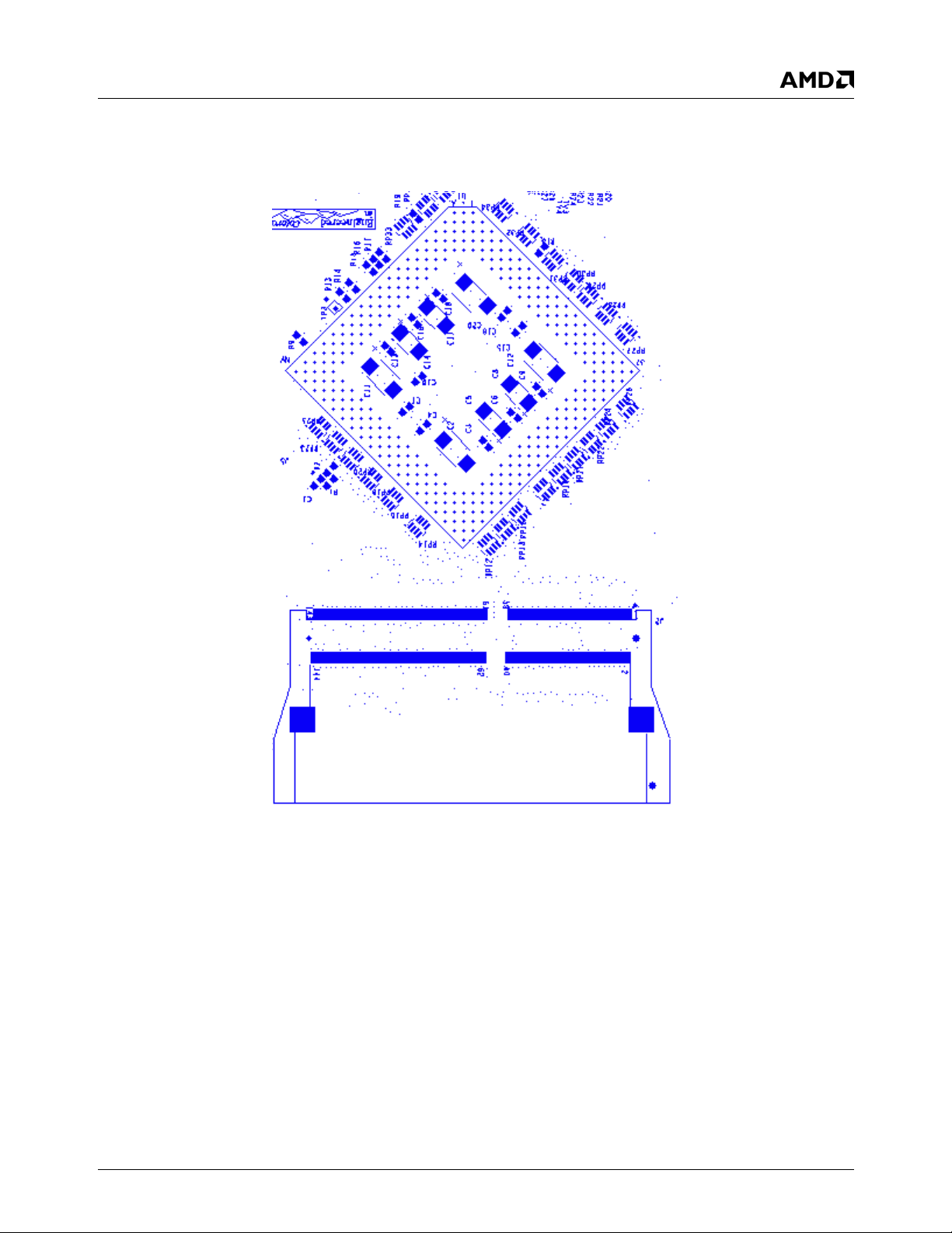
Figure A-11. Placement of SODIMM with SPGA
AMD Geode™ GX1 Processor PC133 Layout Recommendations 25
Page 26

Application Note
Revision 3.0 - June 2001 - Confidential
A.3 Definitions
5-5 Routing or 6-6 Routing: This nomenclature refers to the trace width and trace spacing, respectively, which is being
used to route signals. The first number refers to the trace width (i.e., 5 MILs or 6 MILs), while the second number refers to
the edge-to-edge spacing. Note that this is NOT the centerline-to-centerline spacing, which would actually be edge-to-edge
spacing plus an additional trace width.
2H Spacing: H is the height of microstrip above the plane. “2H spacing” refers to a trace-to-trace separation (between
edges, not centerlines) of twice the specified height above the reference plane. Alternatively, 1H spacing refers to a traceto-trace separation equal to the height above the reference plane. Smaller separations between traces (relative to H) lead
to greater mutual coupling, both capacitively and inductively . This directly affects the amount of crosstalk receiv ed from one
trace to another and has a detrimental effect on signal quality.
Crosstalk: When electrical signals travel along copper etch, they generate both electric fields and magnetic fields. The
electric fields tend to generate an opposite charge buildup in nearby conductors, thereby leading to capacitive coupling of
signal traces. Magnetic fields are created due to current flowing in a trace. These magnetic fields in turn induce currents
and voltages in other nearby conductors. Either of these coupling mechanisms can affect the intended signals on nearby
conductors by either adding to the existing waveform or subtracting from it. At some point in time, an incident wave front
may be observed at a given point along an aggressor trace. The effects of this wavefront on other nearby traces can be
measured. Inductive coupling has opposite polarities in th e forward and reverse directions (toward the load and away from
it at a given point along the victim trace). However, capacitive coupling has the same polarity in both directions. Because of
this, the forward capacitive and inductive crosstalk components nearly cancel. Reverse crosstalk, however, is roughly the
sum of the two. A series terminating resistor at the driver extinguishes both the reverse crosstalk component and the reflection of the incident waveform from the load when it arrives back at the termination.
Coupling Coefficient: The amount of crosstalk depends not only on the separation of traces from each other, but also on
rise times and length of parallel travel. The nominal coupling coefficient, expressed as a percentage received of the aggressor signal, is as follows:
2
K / (1 + (D/H)
)
Where:
D is centerline-to-centerline trace spacing (NOT edge-to-edge),
H is the height above the reference plane, and
K is a constant which depends on the rise time and length of coupling, and is always < 1.
K is usually determined empirically by comparing the impressed voltage waveform to the driven wavef orm, then accounting
for the 1 / (1 + (D/H)
2
) factor. For higher D/H ratios, the coupling coefficient is indirectly propor tiona l to ~ D2. This is why a
2X increase in spacing accounts for roughly a 4X decrease in the coupling coefficient. Coupling coefficients less than 3%
are ideal for most digital systems.
Critical Length: The critical length of a signal is defined as one-sixth the el ectrical length of the r ising edge, and defines
the boundary between lumped and distr ibuted systems. In other words, if the trace is short enough compared to the (electrical) length of the rising edge, all points on the line will see a nearly uniform transition from V(10%) to V(90%). If, however,
the trace is longer than the critical length, then different points along a transmission line will see different voltages at a given
time since the incident waveform takes longer to tra v el to further points along the line. Traces which are longer than the critical length or are not good transmission lines exhibit ringing. Distributed systems always ring without proper termination,
while lumped systems may ring depend upon the damping factor of the transmission line. The bottom line is that high speed
digital signaling effects need to be accounted for when traces are routed a dista nce to a loa d which is mo re than thei r critical length. Some examples:
For a 2 ns rise time on microstrip and T
For a 1 ns rise time on stripline, T
≈ 174 ps/inch, L
P
≈ 138 ps/inch, L
P
CRITICAL(inches)
CRITICAL(inches)
= T
= T
RISE
/ (TP * 6), or ~2.4 inches.
RISE
/ (TP * 6), or ~0.96 inches.
26 AMD Geode™ GX1 Processor PC133 Layout Recommendations
Page 27
© 2004 Advanced Micro Devices, Inc. All rights reserved.
The contents of this document are provided in connection with Advanced Micro
Devices, Inc. (“AMD”) products. AMD makes no representations or warranties with
respect to the accuracy or completeness of the contents of this publication and
reserves the right to make changes to specifications and product descriptions at
any time without notice. No license, whether express, implied, arising by estoppel
or otherwise, to any intellectual property rights is granted by this publication.
Except as set forth in AMD’s Standard Terms and Conditions of Sale, AMD
assumes no liability whatsoever, and disclaims any express or implied warranty,
relating to its products including, but not limited to, the implied warranty of merchantability, fitness for a particular purpose, or infringement of any intellectual
property right.
AMD’s products are not designed, intended, authorized or warranted for use as
components in systems intended for surgical implant into the body, or in other
applications intended to support or sustain life, or in any other application in which
the failure of AMD’s product could create a situation where personal injury, death,
or severe property or environmental damage ma y occur. AMD reserves the right to
discontinue or make changes to its products at an y time wi thout noti ce.
www.amd.com
One AMD Place
P.O. Box 3453,
Sunnyvale, CA 94088-3453 USA
Tel: 408-732-2400 or 800-538-8450
TWX: 910-339-9280
TELEX: 34-6306
TECHNICAL SUPPORT
USA & Canada: 800-222-9323 or 408-749-5703
USA & Canada: PC Microprocessor: 408-749-3060
USA & Canada Email: [email protected]
Latin America Email: [email protected]
Argentina: 001-800-200-1111, after tone 800-859-4478
Chile: 800-532-853
Mexico: 95-800-222-9323
Europe & UK: +44–0-1276-803299
Fax: +44–0-1276-803298
France: 0800-908-621
Germany: +49–89-450-53199
Italy: 800-877224
Europe Email: [email protected]
Far East Fax: 852-2956-0588
Japan Fax: 81-3-3346-7848
TRADEMARKS
AMD, the AMD Arrow logo, and combinations
thereof and Geode are trademarks of
Advanced Micro Devices, Inc.
Other product names used in this publication are
for identification purposes only and may be trademarks of their respective companies.
 Loading...