

Datasheet AMD-K6-300AFR, AMD-K6-266AFR, AMD-K6-233AFR, AMD-K6-200AFR, AMD-K6-233ANR Datasheet (AMD Advanced Micro Devices)
...
Preliminary Information
AMD-K6
Processor
Data Sheet
®

Preliminary Information
© 1998 Advanced Micro Devices, Inc. All rights reserved.
Advanced Micro Devices, Inc. (“AMD”) reserves the right to make changes in its
products without notice in order to improve design or performance characteristics.
The information in this publication is believed to be accurate at the time of
publication, but AMD makes no representations or warranties with respect to the
accuracy or completeness of the contents of this publication or the information
contained herein, and reserves the right to make changes at any time, without notice.
AMD disclaims responsibility for any consequences resulting from the use of the
information included in this publication.
This publication neither states nor implies any representations or warranties of any
kind, including but not limited to, any implied warranty of merchantability or fitness
for a particular purpose. AMD products are not authorized for use as critical
components in life support devices or systems without AMD’s written approval. AMD
assumes no liability whatsoever for claims associated with the sale or use (including
the use of engineering samples) of AMD products, except as provided in AMD’s Terms
and Conditions of Sale for such products.
Trademarks
AMD, the AMD logo, and combinations thereof, K86, AMD-K5, and the AMD-K6 logo are trademarks, and RISC86
and AMD-K6 are registered trademarks of Advanced Micro Devices, Inc.
Microsoft and Windows are registered trademarks, and Windows NT is a trademark of Microsoft Corporation.
Netware is a registered trademark of Novell, Inc.
MMX is a trademark and Pentium is a registered trademark of Intel Corporation.
The TAP State Diagram is reprinted from IEEE Std 1149.1-1990 “IEEE Standard Test Access Port and Boundary-Scan
Architecture,” Copyright © 1990 by the Institute of Electrical and Electronics Engineers, Inc. The IEEE disclaims
any responsibility or liability resulting from the placement and use in the described manner. Information is reprinted
with the permission of the IEEE.
Other product names used in this publication are for identification purposes only and may be trademarks of their
respective companies.

Contents iii
20695H/0—March 1998 AMD-K6
®
Processor Data Sheet
Preliminary Information
Contents
Revision History . . . . . . . . . . . . . . . . . . . . . . . . . . . . . . . . . . . . . . . . . xvii
About This Data Sheet . . . . . . . . . . . . . . . . . . . . . . . . . . . . . . . . . . . . . . 1
Part One
AMD-K6® Processor Family 3
1 AMD-K6® Processor . . . . . . . . . . . . . . . . . . . . . . . . . . . . . . . . . . 5
2 Internal Architecture . . . . . . . . . . . . . . . . . . . . . . . . . . . . . . . . . 7
2.1 Introduction . . . . . . . . . . . . . . . . . . . . . . . . . . . . . . . . . . . . . . . . 7
2.2 AMD-K6
®
Processor Microarchitecture Overview . . . . . . . . . 7
Enhanced RISC86
®
Microarchitecture . . . . . . . . . . . . . . . . . . . 8
2.3 Cache, Instruction Prefetch, and Predecode Bits . . . . . . . . . 11
Cache . . . . . . . . . . . . . . . . . . . . . . . . . . . . . . . . . . . . . . . . . . . . . 11
Prefetching. . . . . . . . . . . . . . . . . . . . . . . . . . . . . . . . . . . . . . . . . 12
Predecode Bits. . . . . . . . . . . . . . . . . . . . . . . . . . . . . . . . . . . . . . 12
2.4 Instruction Fetch and Decode . . . . . . . . . . . . . . . . . . . . . . . . . 13
Instruction Fetch . . . . . . . . . . . . . . . . . . . . . . . . . . . . . . . . . . . . 13
Instruction Decode . . . . . . . . . . . . . . . . . . . . . . . . . . . . . . . . . . 14
2.5 Centralized Scheduler . . . . . . . . . . . . . . . . . . . . . . . . . . . . . . . 16
2.6 Execution Units . . . . . . . . . . . . . . . . . . . . . . . . . . . . . . . . . . . . 17
2.7 Branch-Prediction Logic . . . . . . . . . . . . . . . . . . . . . . . . . . . . . 19
Branch History Table. . . . . . . . . . . . . . . . . . . . . . . . . . . . . . . . . 19
Branch Target Cache . . . . . . . . . . . . . . . . . . . . . . . . . . . . . . . . . 19
Return Address Stack . . . . . . . . . . . . . . . . . . . . . . . . . . . . . . . . 20
Branch Execution Unit . . . . . . . . . . . . . . . . . . . . . . . . . . . . . . . 20
3 Software Environment . . . . . . . . . . . . . . . . . . . . . . . . . . . . . . . 21
3.1 Registers . . . . . . . . . . . . . . . . . . . . . . . . . . . . . . . . . . . . . . . . . . 21
General-Purpose Registers. . . . . . . . . . . . . . . . . . . . . . . . . . . . 21
Integer Data Types . . . . . . . . . . . . . . . . . . . . . . . . . . . . . . . . . . 23
Segment Registers. . . . . . . . . . . . . . . . . . . . . . . . . . . . . . . . . . . 24
Segment Usage . . . . . . . . . . . . . . . . . . . . . . . . . . . . . . . . . . . . . 24
Instruction Pointer . . . . . . . . . . . . . . . . . . . . . . . . . . . . . . . . . . 25
Floating-Point Registers . . . . . . . . . . . . . . . . . . . . . . . . . . . . . . 25
Floating-Point Register Data Types. . . . . . . . . . . . . . . . . . . . . 28
MMX™ Registers. . . . . . . . . . . . . . . . . . . . . . . . . . . . . . . . . . . . 29
EFLAGS Register . . . . . . . . . . . . . . . . . . . . . . . . . . . . . . . . . . . 31
Control Registers. . . . . . . . . . . . . . . . . . . . . . . . . . . . . . . . . . . . 32
Debug Registers. . . . . . . . . . . . . . . . . . . . . . . . . . . . . . . . . . . . . 34
Model-Specific Registers (MSR) . . . . . . . . . . . . . . . . . . . . . . . 37

iv Contents
AMD-K6® Processor Data Sheet 20695H/0—March 1998
Preliminary Information
Memory Management Registers . . . . . . . . . . . . . . . . . . . . . . .39
Task State Segment. . . . . . . . . . . . . . . . . . . . . . . . . . . . . . . . . . 41
Paging . . . . . . . . . . . . . . . . . . . . . . . . . . . . . . . . . . . . . . . . . . . . . 42
Descriptors and Gates. . . . . . . . . . . . . . . . . . . . . . . . . . . . . . . . 45
Exceptions and Interrupts . . . . . . . . . . . . . . . . . . . . . . . . . . . . 48
3.2 Instructions Supported by the AMD-K6 Processor . . . . . . . . 49
4 Logic Symbol Diagram . . . . . . . . . . . . . . . . . . . . . . . . . . . . . . . 77
5 Signal Descriptions . . . . . . . . . . . . . . . . . . . . . . . . . . . . . . . . . . 79
5.1 A20M# (Address Bit 20 Mask) . . . . . . . . . . . . . . . . . . . . . . . . . 79
5.2 A[31:3] (Address Bus) . . . . . . . . . . . . . . . . . . . . . . . . . . . . . . . 80
5.3 ADS# (Address Strobe) . . . . . . . . . . . . . . . . . . . . . . . . . . . . . . 81
5.4 ADSC# (Address Strobe Copy) . . . . . . . . . . . . . . . . . . . . . . . .81
5.5 AHOLD (Address Hold) . . . . . . . . . . . . . . . . . . . . . . . . . . . . . . 82
5.6 AP (Address Parity) . . . . . . . . . . . . . . . . . . . . . . . . . . . . . . . . . 83
5.7 APCHK# (Address Parity Check) . . . . . . . . . . . . . . . . . . . . . . 84
5.8 BE[7:0]# (Byte Enables) . . . . . . . . . . . . . . . . . . . . . . . . . . . . . . 85
5.9 BF[2:0] (Bus Frequency) . . . . . . . . . . . . . . . . . . . . . . . . . . . . .86
5.10 BOFF# (Backoff) . . . . . . . . . . . . . . . . . . . . . . . . . . . . . . . . . . . . 87
5.11 BRDY# (Burst Ready) . . . . . . . . . . . . . . . . . . . . . . . . . . . . . . . 88
5.12 BRDYC# (Burst Ready Copy) . . . . . . . . . . . . . . . . . . . . . . . . . 89
5.13 BREQ (Bus Request) . . . . . . . . . . . . . . . . . . . . . . . . . . . . . . . . 90
5.14 CACHE# (Cacheable Access) . . . . . . . . . . . . . . . . . . . . . . . . . 90
5.15 CLK (Clock) . . . . . . . . . . . . . . . . . . . . . . . . . . . . . . . . . . . . . . . 91
5.16 D/C# (Data/Code) . . . . . . . . . . . . . . . . . . . . . . . . . . . . . . . . . . . 91
5.17 D[63:0] (Data Bus) . . . . . . . . . . . . . . . . . . . . . . . . . . . . . . . . . . 92
5.18 DP[7:0] (Data Parity) . . . . . . . . . . . . . . . . . . . . . . . . . . . . . . . . 93
5.19 EADS# (External Address Strobe) . . . . . . . . . . . . . . . . . . . . . 94
5.20 EWBE# (External Write Buffer Empty) . . . . . . . . . . . . . . . . . 95
5.21 FERR# (Floating-Point Error) . . . . . . . . . . . . . . . . . . . . . . . . 96
5.22 FLUSH# (Cache Flush) . . . . . . . . . . . . . . . . . . . . . . . . . . . . . . 97
5.23 HIT# (Inquire Cycle Hit) . . . . . . . . . . . . . . . . . . . . . . . . . . . . . 98
5.24 HITM# (Inquire Cycle Hit To Modified Line) . . . . . . . . . . . . 98
5.25 HLDA (Hold Acknowledge) . . . . . . . . . . . . . . . . . . . . . . . . . .99
5.26 HOLD (Bus Hold Request) . . . . . . . . . . . . . . . . . . . . . . . . . . . 99
5.27 IGNNE# (Ignore Numeric Exception) . . . . . . . . . . . . . . . . . 100
5.28 INIT (Initialization) . . . . . . . . . . . . . . . . . . . . . . . . . . . . . . . . 101
5.29 INTR (Maskable Interrupt) . . . . . . . . . . . . . . . . . . . . . . . . . . 102
5.30 INV (Invalidation Request) . . . . . . . . . . . . . . . . . . . . . . . . . . 102
5.31 KEN# (Cache Enable) . . . . . . . . . . . . . . . . . . . . . . . . . . . . . . 103
5.32 LOCK# (Bus Lock) . . . . . . . . . . . . . . . . . . . . . . . . . . . . . . . . . 104
5.33 M/IO# (Memory or I/O) . . . . . . . . . . . . . . . . . . . . . . . . . . . . . 105
5.34 NA# (Next Address) . . . . . . . . . . . . . . . . . . . . . . . . . . . . . . . . 106
5.35 NMI (Non-Maskable Interrupt) . . . . . . . . . . . . . . . . . . . . . . . 106
5.36 PCD (Page Cache Disable) . . . . . . . . . . . . . . . . . . . . . . . . . . 107
5.37 PCHK# (Parity Check) . . . . . . . . . . . . . . . . . . . . . . . . . . . . . . 108
5.38 PWT (Page Writethrough) . . . . . . . . . . . . . . . . . . . . . . . . . . . 109

Contents v
20695H/0—March 1998 AMD-K6
®
Processor Data Sheet
Preliminary Information
5.39 RESET (Reset) . . . . . . . . . . . . . . . . . . . . . . . . . . . . . . . . . . . . 110
5.40 RSVD (Reserved) . . . . . . . . . . . . . . . . . . . . . . . . . . . . . . . . . . 110
5.41 SCYC (Split Cycle) . . . . . . . . . . . . . . . . . . . . . . . . . . . . . . . . . 111
5.42 SMI# (System Management Interrupt) . . . . . . . . . . . . . . . . 111
5.43 SMIACT# (System Management Interrupt Active) . . . . . . 112
5.44 STPCLK# (Stop Clock) . . . . . . . . . . . . . . . . . . . . . . . . . . . . . . 113
5.45 TCK (Test Clock) . . . . . . . . . . . . . . . . . . . . . . . . . . . . . . . . . . 113
5.46 TDI (Test Data Input) . . . . . . . . . . . . . . . . . . . . . . . . . . . . . . 114
5.47 TDO (Test Data Output) . . . . . . . . . . . . . . . . . . . . . . . . . . . . 114
5.48 TMS (Test Mode Select) . . . . . . . . . . . . . . . . . . . . . . . . . . . . 114
5.49 TRST# (Test Reset) . . . . . . . . . . . . . . . . . . . . . . . . . . . . . . . . 115
5.50 VCC2DET (V
CC2
Detect) . . . . . . . . . . . . . . . . . . . . . . . . . . . . 115
5.51 W/R# (Write/Read) . . . . . . . . . . . . . . . . . . . . . . . . . . . . . . . . . 115
5.52 WB/WT# (Writeback or Writethrough) . . . . . . . . . . . . . . . . 116
6 Bus Cycles . . . . . . . . . . . . . . . . . . . . . . . . . . . . . . . . . . . . . . . . 121
6.1 Timing Diagrams . . . . . . . . . . . . . . . . . . . . . . . . . . . . . . . . . . 121
6.2 Bus State Machine Diagram . . . . . . . . . . . . . . . . . . . . . . . . . 123
Idle . . . . . . . . . . . . . . . . . . . . . . . . . . . . . . . . . . . . . . . . . . . . . . 124
Address. . . . . . . . . . . . . . . . . . . . . . . . . . . . . . . . . . . . . . . . . . . 124
Data. . . . . . . . . . . . . . . . . . . . . . . . . . . . . . . . . . . . . . . . . . . . . . 124
Data-NA# Requested . . . . . . . . . . . . . . . . . . . . . . . . . . . . . . . . 124
Pipeline Address . . . . . . . . . . . . . . . . . . . . . . . . . . . . . . . . . . . 124
Pipeline Data . . . . . . . . . . . . . . . . . . . . . . . . . . . . . . . . . . . . . . 125
Transition . . . . . . . . . . . . . . . . . . . . . . . . . . . . . . . . . . . . . . . . . 125
6.3 Memory Reads and Writes . . . . . . . . . . . . . . . . . . . . . . . . . . 126
Single-Transfer Memory Read and Write . . . . . . . . . . . . . . . 126
Misaligned Single-Transfer Memory Read and Write . . . . . 128
Burst Reads and Pipelined Burst Reads . . . . . . . . . . . . . . . . 130
Burst Writeback. . . . . . . . . . . . . . . . . . . . . . . . . . . . . . . . . . . . 132
6.4 I/O Read and Write . . . . . . . . . . . . . . . . . . . . . . . . . . . . . . . . 134
Basic I/O Read and Write . . . . . . . . . . . . . . . . . . . . . . . . . . . . 134
Misaligned I/O Read and Write . . . . . . . . . . . . . . . . . . . . . . . 135
6.5 Inquire and Bus Arbitration Cycles . . . . . . . . . . . . . . . . . . . 136
Hold and Hold Acknowledge Cycle . . . . . . . . . . . . . . . . . . . . 136
HOLD-Initiated Inquire Hit to Shared or Exclusive
Line . . . . . . . . . . . . . . . . . . . . . . . . . . . . . . . . . . . . . . . . . . . . . . 138
HOLD-Initiated Inquire Hit to Modified Line . . . . . . . . . . . 140
AHOLD-Initiated Inquire Miss. . . . . . . . . . . . . . . . . . . . . . . . 142
AHOLD-Initiated Inquire Hit to Shared or Exclusive
Line . . . . . . . . . . . . . . . . . . . . . . . . . . . . . . . . . . . . . . . . . . . . . 144
AHOLD-Initiated Inquire Hit to Modified Line. . . . . . . . . . 146
AHOLD Restriction . . . . . . . . . . . . . . . . . . . . . . . . . . . . . . . . . 148
Bus Backoff (BOFF#) . . . . . . . . . . . . . . . . . . . . . . . . . . . . . . . . 150
Locked Cycles . . . . . . . . . . . . . . . . . . . . . . . . . . . . . . . . . . . . . 152
Basic Locked Operation . . . . . . . . . . . . . . . . . . . . . . . . . . . . . 152
Locked Operation with BOFF# Intervention . . . . . . . . . . . . 154
Interrupt Acknowledge. . . . . . . . . . . . . . . . . . . . . . . . . . . . . . 156

vi Contents
AMD-K6® Processor Data Sheet 20695H/0—March 1998
Preliminary Information
6.6 Special Bus Cycles . . . . . . . . . . . . . . . . . . . . . . . . . . . . . . . . . 158
Basic Special Bus Cycle . . . . . . . . . . . . . . . . . . . . . . . . . . . . . 158
Shutdown Cycle. . . . . . . . . . . . . . . . . . . . . . . . . . . . . . . . . . . . 160
Stop Grant and Stop Clock States . . . . . . . . . . . . . . . . . . . . . 161
INIT-Initiated Transition from Protected Mode to
Real Mode . . . . . . . . . . . . . . . . . . . . . . . . . . . . . . . . . . . . . . . . 164
7 Power-on Configuration and Initialization . . . . . . . . . . . . . . 167
7.1 Signals Sampled During the Falling Transition
of RESET . . . . . . . . . . . . . . . . . . . . . . . . . . . . . . . . . . . . . . . . . 167
FLUSH# . . . . . . . . . . . . . . . . . . . . . . . . . . . . . . . . . . . . . . . . . . 167
BF[2:0] . . . . . . . . . . . . . . . . . . . . . . . . . . . . . . . . . . . . . . . . . . . 167
BRDYC# . . . . . . . . . . . . . . . . . . . . . . . . . . . . . . . . . . . . . . . . . . 167
7.2 RESET Requirements . . . . . . . . . . . . . . . . . . . . . . . . . . . . . . 168
7.3 State of Processor After RESET . . . . . . . . . . . . . . . . . . . . . . 168
Output Signals . . . . . . . . . . . . . . . . . . . . . . . . . . . . . . . . . . . . . 168
Registers. . . . . . . . . . . . . . . . . . . . . . . . . . . . . . . . . . . . . . . . . . 168
7.4 State of Processor After INIT . . . . . . . . . . . . . . . . . . . . . . . . 170
8 Cache Organization . . . . . . . . . . . . . . . . . . . . . . . . . . . . . . . . . 171
8.1 MESI States in the Data Cache . . . . . . . . . . . . . . . . . . . . . . . 172
8.2 Predecode Bits . . . . . . . . . . . . . . . . . . . . . . . . . . . . . . . . . . . . 172
8.3 Cache Operation . . . . . . . . . . . . . . . . . . . . . . . . . . . . . . . . . . . 173
Cache-Related Signals . . . . . . . . . . . . . . . . . . . . . . . . . . . . . . 175
8.4 Cache Disabling . . . . . . . . . . . . . . . . . . . . . . . . . . . . . . . . . . . 175
8.5 Cache-Line Fills . . . . . . . . . . . . . . . . . . . . . . . . . . . . . . . . . . . 176
8.6 Cache-Line Replacements . . . . . . . . . . . . . . . . . . . . . . . . . . . 177
8.7 Write Allocate . . . . . . . . . . . . . . . . . . . . . . . . . . . . . . . . . . . . . 177
Write to a Cacheable Page . . . . . . . . . . . . . . . . . . . . . . . . . . . 178
Write to a Sector . . . . . . . . . . . . . . . . . . . . . . . . . . . . . . . . . . . 178
Write Allocate Limit . . . . . . . . . . . . . . . . . . . . . . . . . . . . . . . . 178
Descriptions of the Logic Mechanisms and Conditions. . . . 180
8.8 Prefetching . . . . . . . . . . . . . . . . . . . . . . . . . . . . . . . . . . . . . . . 181
8.9 Cache States . . . . . . . . . . . . . . . . . . . . . . . . . . . . . . . . . . . . . . 182
8.10 Cache Coherency . . . . . . . . . . . . . . . . . . . . . . . . . . . . . . . . . . 183
Inquire Cycles . . . . . . . . . . . . . . . . . . . . . . . . . . . . . . . . . . . . . 183
Internal Snooping . . . . . . . . . . . . . . . . . . . . . . . . . . . . . . . . . . 183
FLUSH# . . . . . . . . . . . . . . . . . . . . . . . . . . . . . . . . . . . . . . . . . . 184
WBINVD and INVD. . . . . . . . . . . . . . . . . . . . . . . . . . . . . . . . . 184
Cache-Line Replacement . . . . . . . . . . . . . . . . . . . . . . . . . . . . 184
Cache Snooping . . . . . . . . . . . . . . . . . . . . . . . . . . . . . . . . . . . . 186
8.11 Writethrough vs. Writeback Coherency States . . . . . . . . . . 187
8.12 A20M# Masking of Cache Accesses . . . . . . . . . . . . . . . . . . . 187
9 Floating-Point and Multimedia Execution Units . . . . . . . . . 189
9.1 Floating-Point Execution Unit . . . . . . . . . . . . . . . . . . . . . . . 189
Handling Floating-Point Exceptions . . . . . . . . . . . . . . . . . . . 189
External Logic Support of Floating-Point Exceptions . . . . . 189

Contents vii
20695H/0—March 1998 AMD-K6
®
Processor Data Sheet
Preliminary Information
9.2 Multimedia Execution Unit . . . . . . . . . . . . . . . . . . . . . . . . . . 191
9.3 Floating-Point and MMX Instruction Compatibility . . . . . . 191
Registers. . . . . . . . . . . . . . . . . . . . . . . . . . . . . . . . . . . . . . . . . . 191
Exceptions . . . . . . . . . . . . . . . . . . . . . . . . . . . . . . . . . . . . . . . . 191
FERR# and IGNNE# . . . . . . . . . . . . . . . . . . . . . . . . . . . . . . . . 191
10 System Management Mode (SMM) . . . . . . . . . . . . . . . . . . . . 193
10.1 Overview . . . . . . . . . . . . . . . . . . . . . . . . . . . . . . . . . . . . . . . . . 193
10.2 SMM Operating Mode and Default Register Values . . . . . 193
10.3 SMM State-Save Area . . . . . . . . . . . . . . . . . . . . . . . . . . . . . . 196
10.4 SMM Revision Identifier . . . . . . . . . . . . . . . . . . . . . . . . . . . . 198
10.5 SMM Base Address . . . . . . . . . . . . . . . . . . . . . . . . . . . . . . . . . 199
10.6 Halt Restart Slot . . . . . . . . . . . . . . . . . . . . . . . . . . . . . . . . . . . 199
10.7 I/O Trap Dword . . . . . . . . . . . . . . . . . . . . . . . . . . . . . . . . . . . . 200
10.8 I/O Trap Restart Slot . . . . . . . . . . . . . . . . . . . . . . . . . . . . . . . 201
10.9 Exceptions, Interrupts, and Debug in SMM . . . . . . . . . . . . 202
11 Test and Debug . . . . . . . . . . . . . . . . . . . . . . . . . . . . . . . . . . . . 203
11.1 Built-In Self-Test (BIST) . . . . . . . . . . . . . . . . . . . . . . . . . . . . 203
11.2 Tri-State Test Mode . . . . . . . . . . . . . . . . . . . . . . . . . . . . . . . . 204
11.3 Boundary-Scan Test Access Port (TAP) . . . . . . . . . . . . . . . . 205
Test Access Port . . . . . . . . . . . . . . . . . . . . . . . . . . . . . . . . . . . . 205
TAP Signals . . . . . . . . . . . . . . . . . . . . . . . . . . . . . . . . . . . . . . . 205
TAP Registers . . . . . . . . . . . . . . . . . . . . . . . . . . . . . . . . . . . . . 206
TAP Instructions . . . . . . . . . . . . . . . . . . . . . . . . . . . . . . . . . . . 211
TAP Controller State Machine . . . . . . . . . . . . . . . . . . . . . . . . 212
11.4 L1 Cache Inhibit . . . . . . . . . . . . . . . . . . . . . . . . . . . . . . . . . . . 215
Purpose. . . . . . . . . . . . . . . . . . . . . . . . . . . . . . . . . . . . . . . . . . . 215
11.5 Debug . . . . . . . . . . . . . . . . . . . . . . . . . . . . . . . . . . . . . . . . . . . . 216
Debug Registers. . . . . . . . . . . . . . . . . . . . . . . . . . . . . . . . . . . . 216
Debug Exceptions . . . . . . . . . . . . . . . . . . . . . . . . . . . . . . . . . .221
12 Clock Control . . . . . . . . . . . . . . . . . . . . . . . . . . . . . . . . . . . . . . 223
12.1 Halt State . . . . . . . . . . . . . . . . . . . . . . . . . . . . . . . . . . . . . . . . 224
Enter Halt State . . . . . . . . . . . . . . . . . . . . . . . . . . . . . . . . . . . 224
Exit Halt State . . . . . . . . . . . . . . . . . . . . . . . . . . . . . . . . . . . . . 224
12.2 Stop Grant State . . . . . . . . . . . . . . . . . . . . . . . . . . . . . . . . . . . 225
Enter Stop Grant State . . . . . . . . . . . . . . . . . . . . . . . . . . . . . . 225
Exit Stop Grant State . . . . . . . . . . . . . . . . . . . . . . . . . . . . . . . 225
12.3 Stop Grant Inquire State . . . . . . . . . . . . . . . . . . . . . . . . . . . . 226
Enter Stop Grant Inquire State . . . . . . . . . . . . . . . . . . . . . . . 226
Exit Stop Grant Inquire State . . . . . . . . . . . . . . . . . . . . . . . . 226
12.4 Stop Clock State . . . . . . . . . . . . . . . . . . . . . . . . . . . . . . . . . . . 226
Enter Stop Clock State . . . . . . . . . . . . . . . . . . . . . . . . . . . . . . 226
Exit Stop Clock State . . . . . . . . . . . . . . . . . . . . . . . . . . . . . . . 227

viii Contents
AMD-K6® Processor Data Sheet 20695H/0—March 1998
Preliminary Information
13 Power and Grounding . . . . . . . . . . . . . . . . . . . . . . . . . . . . . . . 229
13.1 Power Connections . . . . . . . . . . . . . . . . . . . . . . . . . . . . . . . . . 229
13.2 Decoupling Recommendations . . . . . . . . . . . . . . . . . . . . . . . 230
13.3 Pin Connection Requirements . . . . . . . . . . . . . . . . . . . . . . . 231
14 Electrical Data . . . . . . . . . . . . . . . . . . . . . . . . . . . . . . . . . . . . . 233
14.1 Operating Ranges . . . . . . . . . . . . . . . . . . . . . . . . . . . . . . . . . . 233
14.2 Absolute Ratings . . . . . . . . . . . . . . . . . . . . . . . . . . . . . . . . . . 233
14.3 DC Characteristics . . . . . . . . . . . . . . . . . . . . . . . . . . . . . . . . . 234
14.4 Power Dissipation . . . . . . . . . . . . . . . . . . . . . . . . . . . . . . . . . . 235
15 I/O Buffer Characteristics . . . . . . . . . . . . . . . . . . . . . . . . . . . 237
15.1 Selectable Drive Strength . . . . . . . . . . . . . . . . . . . . . . . . . . . 237
15.2 I/O Buffer Model . . . . . . . . . . . . . . . . . . . . . . . . . . . . . . . . . . . 238
15.3 I/O Model Application Note . . . . . . . . . . . . . . . . . . . . . . . . . 239
15.4 I/O Buffer AC and DC Characteristics . . . . . . . . . . . . . . . . . 239
16 Signal Switching Characteristics . . . . . . . . . . . . . . . . . . . . . . 241
16.1 CLK Switching Characteristics . . . . . . . . . . . . . . . . . . . . . . . 241
16.2 Clock Switching Characteristics for 66-MHz Bus
Operation . . . . . . . . . . . . . . . . . . . . . . . . . . . . . . . . . . . . . . . . 242
16.3 Clock Switching Characteristics for 60-MHz Bus
Operation . . . . . . . . . . . . . . . . . . . . . . . . . . . . . . . . . . . . . . . . 242
16.4 Valid Delay, Float, Setup, and Hold Timings . . . . . . . . . . . 243
16.5 Output Delay Timings for 66-MHz Bus Operation . . . . . . . 244
16.6 Input Setup and Hold Timings for 66-MHz Bus
Operation . . . . . . . . . . . . . . . . . . . . . . . . . . . . . . . . . . . . . . . . 246
16.7 Output Delay Timings for 60-MHz Bus Operation . . . . . . . 248
16.8 Input Setup and Hold Timings for 60-MHz Bus
Operation . . . . . . . . . . . . . . . . . . . . . . . . . . . . . . . . . . . . . . . . 250
16.9 RESET and Test Signal Timing . . . . . . . . . . . . . . . . . . . . . . 252
17 Thermal Design . . . . . . . . . . . . . . . . . . . . . . . . . . . . . . . . . . . . 259
17.1 Package Thermal Specifications . . . . . . . . . . . . . . . . . . . . . . 259
Heat Dissipation Path . . . . . . . . . . . . . . . . . . . . . . . . . . . . . . . 261
Measuring Case Temperature . . . . . . . . . . . . . . . . . . . . . . . . 262
17.2 Layout and Airflow Considerations . . . . . . . . . . . . . . . . . . . 262
Voltage Regulator . . . . . . . . . . . . . . . . . . . . . . . . . . . . . . . . . . 262
Airflow Management in a System Design. . . . . . . . . . . . . . . 264
18 Pin Description Diagram . . . . . . . . . . . . . . . . . . . . . . . . . . . . 267
19 Pin Designations . . . . . . . . . . . . . . . . . . . . . . . . . . . . . . . . . . . 269
20 Package Specifications . . . . . . . . . . . . . . . . . . . . . . . . . . . . . . 271
20.1 321-Pin Staggered CPGA Package Specification . . . . . . . . 271
21 Ordering Information . . . . . . . . . . . . . . . . . . . . . . . . . . . . . . . 273

Contents ix
20695H/0—March 1998 AMD-K6
®
Processor Data Sheet
Preliminary Information
Part Two
AMD-K6 Processor Model 7 275
22 AMD-K6 Processor . . . . . . . . . . . . . . . . . . . . . . . . . . . . . . . . . 277
23 Internal Architecture . . . . . . . . . . . . . . . . . . . . . . . . . . . . . . . 279
24 Software Environment . . . . . . . . . . . . . . . . . . . . . . . . . . . . . . 281
24.1 Registers . . . . . . . . . . . . . . . . . . . . . . . . . . . . . . . . . . . . . . . . . 281
Model-Specific Registers (MSR) . . . . . . . . . . . . . . . . . . . . . . 281
24.2 Instructions Supported by the AMD-K6 Processor . . . . . . . 283
25 Logic Symbol Diagram . . . . . . . . . . . . . . . . . . . . . . . . . . . . . . 285
26 Signal Descriptions . . . . . . . . . . . . . . . . . . . . . . . . . . . . . . . . . 287
26.1 VCC2DET (V
CC2
Detect) . . . . . . . . . . . . . . . . . . . . . . . . . . . . 287
26.2 VCC2H/L# (V
CC2
High/Low) . . . . . . . . . . . . . . . . . . . . . . . . . 287
27 Bus Cycles . . . . . . . . . . . . . . . . . . . . . . . . . . . . . . . . . . . . . . . . 289
28 Power-on Configuration and Initialization . . . . . . . . . . . . . . 291
28.1 State of Processor After RESET . . . . . . . . . . . . . . . . . . . . . . 291
Output Signals . . . . . . . . . . . . . . . . . . . . . . . . . . . . . . . . . . . . . 291
29 Cache Organization . . . . . . . . . . . . . . . . . . . . . . . . . . . . . . . . . 293
30 Floating-Point and Multimedia Execution Units . . . . . . . . . 295
31 System Management Mode (SMM) . . . . . . . . . . . . . . . . . . . . 297
32 Test and Debug . . . . . . . . . . . . . . . . . . . . . . . . . . . . . . . . . . . . 299
32.1 Tri-State Test Mode . . . . . . . . . . . . . . . . . . . . . . . . . . . . . . . . 299
32.2 Boundary-Scan Test Access Port (TAP) . . . . . . . . . . . . . . . . 299
TAP Registers . . . . . . . . . . . . . . . . . . . . . . . . . . . . . . . . . . . . . 300
33 Clock Control . . . . . . . . . . . . . . . . . . . . . . . . . . . . . . . . . . . . . . 301
34 Power and Grounding . . . . . . . . . . . . . . . . . . . . . . . . . . . . . . . 303
34.1 Power Connections . . . . . . . . . . . . . . . . . . . . . . . . . . . . . . . . . 303
35 Electrical Data . . . . . . . . . . . . . . . . . . . . . . . . . . . . . . . . . . . . . 305
35.1 Operating Ranges . . . . . . . . . . . . . . . . . . . . . . . . . . . . . . . . . . 305
35.2 Absolute Ratings . . . . . . . . . . . . . . . . . . . . . . . . . . . . . . . . . . 305
35.3 DC Characteristics . . . . . . . . . . . . . . . . . . . . . . . . . . . . . . . . . 306
35.4 Power Dissipation . . . . . . . . . . . . . . . . . . . . . . . . . . . . . . . . . . 307
36 I/O Buffer Characteristics . . . . . . . . . . . . . . . . . . . . . . . . . . . 309

x Contents
AMD-K6® Processor Data Sheet 20695H/0—March 1998
Preliminary Information
37 Signal Switching Characteristics . . . . . . . . . . . . . . . . . . . . . . 311
38 Thermal Design . . . . . . . . . . . . . . . . . . . . . . . . . . . . . . . . . . . . 313
38.1 Package Thermal Specifications . . . . . . . . . . . . . . . . . . . . . . 313
39 Pin Description Diagram . . . . . . . . . . . . . . . . . . . . . . . . . . . . 315
40 Pin Designations . . . . . . . . . . . . . . . . . . . . . . . . . . . . . . . . . . . 317
41 Package Specifications . . . . . . . . . . . . . . . . . . . . . . . . . . . . . . 319
42 Ordering Information . . . . . . . . . . . . . . . . . . . . . . . . . . . . . . . 321
Index . . . . . . . . . . . . . . . . . . . . . . . . . . . . . . . . . . . . . . . . . . . . . . . . . . 323

List of Figures xi
20695H/0—March 1998 AMD-K6
®
Processor Data Sheet
Preliminary Information
List of Figures
Part One
AMD-K6 Processor Family 3
Figure 1. AMD-K6 Processor Block Diagram . . . . . . . . . . . . . . . . . . . . . . . 11
Figure 2. Cache Sector Organization . . . . . . . . . . . . . . . . . . . . . . . . . . . . . 12
Figure 3. The Instruction Buffer . . . . . . . . . . . . . . . . . . . . . . . . . . . . . . . . . 13
Figure 4. AMD-K6 Processor Decode Logic . . . . . . . . . . . . . . . . . . . . . . . . 14
Figure 5. AMD-K6 Processor Scheduler. . . . . . . . . . . . . . . . . . . . . . . . . . . 17
Figure 6. EAX Register with 16-Bit and 8-Bit Name Components. . . . . . 22
Figure 7. Integer Data Types. . . . . . . . . . . . . . . . . . . . . . . . . . . . . . . . . . . . 23
Figure 8. Segment Register . . . . . . . . . . . . . . . . . . . . . . . . . . . . . . . . . . . . . 24
Figure 9. Segment Usage . . . . . . . . . . . . . . . . . . . . . . . . . . . . . . . . . . . . . . . 25
Figure 10. Floating-Point Register . . . . . . . . . . . . . . . . . . . . . . . . . . . . . . . . 26
Figure 11. FPU Status Word Register . . . . . . . . . . . . . . . . . . . . . . . . . . . . . 26
Figure 12. FPU Control Word Register . . . . . . . . . . . . . . . . . . . . . . . . . . . . 27
Figure 13. FPU Tag Word Register. . . . . . . . . . . . . . . . . . . . . . . . . . . . . . . . 27
Figure 14. Packed Decimal Data Type . . . . . . . . . . . . . . . . . . . . . . . . . . . . . 28
Figure 15. Precision Real Data Types . . . . . . . . . . . . . . . . . . . . . . . . . . . . . 28
Figure 16. MMX Registers . . . . . . . . . . . . . . . . . . . . . . . . . . . . . . . . . . . . . . . 29
Figure 17. MMX Data Types . . . . . . . . . . . . . . . . . . . . . . . . . . . . . . . . . . . . . 30
Figure 18. EFLAGS Registers . . . . . . . . . . . . . . . . . . . . . . . . . . . . . . . . . . . . 31
Figure 19. Control Register 4 (CR4) . . . . . . . . . . . . . . . . . . . . . . . . . . . . . . . 32
Figure 20. Control Register 3 (CR3) . . . . . . . . . . . . . . . . . . . . . . . . . . . . . . . 32
Figure 21. Control Register 2 (CR2) . . . . . . . . . . . . . . . . . . . . . . . . . . . . . . . 32
Figure 22. Control Register 1 (CR1) . . . . . . . . . . . . . . . . . . . . . . . . . . . . . . . 33
Figure 23. Control Register 0 (CR0) . . . . . . . . . . . . . . . . . . . . . . . . . . . . . . . 33
Figure 24. Debug Register DR7 . . . . . . . . . . . . . . . . . . . . . . . . . . . . . . . . . . 34
Figure 25. Debug Register DR6 . . . . . . . . . . . . . . . . . . . . . . . . . . . . . . . . . . 35
Figure 26. Debug Registers DR5 and DR4. . . . . . . . . . . . . . . . . . . . . . . . . . 35
Figure 27. Debug Registers DR3, DR2, DR1, and DR0. . . . . . . . . . . . . . . . 36
Figure 28. Machine-Check Address Register (MCAR) . . . . . . . . . . . . . . . . 37
Figure 29. Machine-Check Type Register (MCTR). . . . . . . . . . . . . . . . . . . 38
Figure 30. Test Register 12 (TR12) . . . . . . . . . . . . . . . . . . . . . . . . . . . . . . . . 38
Figure 31. Time Stamp Counter (TSC). . . . . . . . . . . . . . . . . . . . . . . . . . . . . 38
Figure 32. Write Handling Control Register (WHCR) . . . . . . . . . . . . . . . . 39
Figure 33. Memory Management Registers. . . . . . . . . . . . . . . . . . . . . . . . . 40
Figure 34. Task State Segment (TSS). . . . . . . . . . . . . . . . . . . . . . . . . . . . . . 41

xii List of Figures
AMD-K6® Processor Data Sheet 20695H/0—March 1998
Preliminary Information
Figure 35. 4-Kbyte Paging Mechanism. . . . . . . . . . . . . . . . . . . . . . . . . . . . .42
Figure 36. 4-Mbyte Paging Mechanism . . . . . . . . . . . . . . . . . . . . . . . . . . . . 43
Figure 37. Page Directory Entry 4-Kbyte Page Table (PDE). . . . . . . . . . . 44
Figure 38. Page Directory Entry 4-Mbyte Page Table (PDE) . . . . . . . . . . 44
Figure 39. Page Table Entry (PTE). . . . . . . . . . . . . . . . . . . . . . . . . . . . . . . . 45
Figure 40. Application Segment Descriptor . . . . . . . . . . . . . . . . . . . . . . . . 46
Figure 41. System Segment Descriptor . . . . . . . . . . . . . . . . . . . . . . . . . . . . 47
Figure 42. Gate Descriptor . . . . . . . . . . . . . . . . . . . . . . . . . . . . . . . . . . . . . . 48
Figure 43. Waveform Definitions . . . . . . . . . . . . . . . . . . . . . . . . . . . . . . . . 122
Figure 44. Bus State Machine Diagram . . . . . . . . . . . . . . . . . . . . . . . . . . . 123
Figure 45. Non-Pipelined Single-Transfer Memory Read/Write and
Write Delayed by EWBE# . . . . . . . . . . . . . . . . . . . . . . . . . . . . . 127
Figure 46. Misaligned Single-Transfer Memory Read and Write . . . . . . 129
Figure 47. Burst Reads and Pipelined Burst Reads . . . . . . . . . . . . . . . . . 131
Figure 48. Burst Writeback due to Cache-Line Replacement . . . . . . . . . 133
Figure 49. Basic I/O Read and Write . . . . . . . . . . . . . . . . . . . . . . . . . . . . . 134
Figure 50. Misaligned I/O Transfer. . . . . . . . . . . . . . . . . . . . . . . . . . . . . . . 135
Figure 51. Basic HOLD/HLDA Operation . . . . . . . . . . . . . . . . . . . . . . . . . 137
Figure 52. HOLD-Initiated Inquire Hit to Shared or Exclusive Line . . . 139
Figure 53. HOLD-Initiated Inquire Hit to Modified Line. . . . . . . . . . . . . 141
Figure 54. AHOLD-Initiated Inquire Miss . . . . . . . . . . . . . . . . . . . . . . . . . 143
Figure 55. AHOLD-Initiated Inquire Hit to Shared or
Exclusive Line . . . . . . . . . . . . . . . . . . . . . . . . . . . . . . . . . . . . . . 145
Figure 56. AHOLD-Initiated Inquire Hit to Modified Line . . . . . . . . . . . 147
Figure 57. AHOLD Restriction . . . . . . . . . . . . . . . . . . . . . . . . . . . . . . . . . . 149
Figure 58. BOFF# Timing. . . . . . . . . . . . . . . . . . . . . . . . . . . . . . . . . . . . . . . 151
Figure 59. Basic Locked Operation. . . . . . . . . . . . . . . . . . . . . . . . . . . . . . . 153
Figure 60. Locked Operation with BOFF# Intervention. . . . . . . . . . . . . . 155
Figure 61. Interrupt Acknowledge Operation . . . . . . . . . . . . . . . . . . . . . . 157
Figure 62. Basic Special Bus Cycle (Halt Cycle) . . . . . . . . . . . . . . . . . . . . 159
Figure 63. Shutdown Cycle . . . . . . . . . . . . . . . . . . . . . . . . . . . . . . . . . . . . .160
Figure 64. Stop Grant and Stop Clock Modes, Part 1 . . . . . . . . . . . . . . . . 162
Figure 65. Stop Grant and Stop Clock Modes, Part 2 . . . . . . . . . . . . . . . . 163
Figure 66. INIT-Initiated Transition from Protected Mode to
Real Mode . . . . . . . . . . . . . . . . . . . . . . . . . . . . . . . . . . . . . . . . . . 165
Figure 67. Cache Organization . . . . . . . . . . . . . . . . . . . . . . . . . . . . . . . . . . 171
Figure 68. Cache Sector Organization . . . . . . . . . . . . . . . . . . . . . . . . . . . . 172
Figure 69. Write Handling Control Register (WHCR) . . . . . . . . . . . . . . . 179
Figure 70. Write Allocate Logic Mechanisms and Conditions. . . . . . . . . 180
Figure 71. External Logic for Supporting Floating-Point
Exceptions . . . . . . . . . . . . . . . . . . . . . . . . . . . . . . . . . . . . . . . . . . 190

List of Figures xiii
20695H/0—March 1998 AMD-K6
®
Processor Data Sheet
Preliminary Information
Figure 72. SMM Memory . . . . . . . . . . . . . . . . . . . . . . . . . . . . . . . . . . . . . . . 195
Figure 73. TAP State Diagram . . . . . . . . . . . . . . . . . . . . . . . . . . . . . . . . . . 213
Figure 74. Debug Register DR7 . . . . . . . . . . . . . . . . . . . . . . . . . . . . . . . . . 217
Figure 75. Debug Register DR6 . . . . . . . . . . . . . . . . . . . . . . . . . . . . . . . . . 218
Figure 76. Debug Registers DR5 and DR4. . . . . . . . . . . . . . . . . . . . . . . . .218
Figure 77. Debug Registers DR3, DR2, DR1, and DR0. . . . . . . . . . . . . . . 219
Figure 78. Clock Control State Transitions . . . . . . . . . . . . . . . . . . . . . . . . 228
Figure 79. Suggested Component Placement . . . . . . . . . . . . . . . . . . . . . . 230
Figure 80. K6STD Pulldown V/I Curves . . . . . . . . . . . . . . . . . . . . . . . . . . . 239
Figure 81. K6STD Pullup V/I Curves . . . . . . . . . . . . . . . . . . . . . . . . . . . . . 239
Figure 82. CLK Waveform . . . . . . . . . . . . . . . . . . . . . . . . . . . . . . . . . . . . . . 243
Figure 83. Diagrams Key . . . . . . . . . . . . . . . . . . . . . . . . . . . . . . . . . . . . . . . 254
Figure 84. Output Valid Delay Timing . . . . . . . . . . . . . . . . . . . . . . . . . . . . 254
Figure 85. Maximum Float Delay Timing . . . . . . . . . . . . . . . . . . . . . . . . . 255
Figure 86. Input Setup and Hold Timing . . . . . . . . . . . . . . . . . . . . . . . . . . 255
Figure 87. Reset and Configuration Timing . . . . . . . . . . . . . . . . . . . . . . . 256
Figure 88. TCK Waveform . . . . . . . . . . . . . . . . . . . . . . . . . . . . . . . . . . . . . . 257
Figure 89. TRST# Timing. . . . . . . . . . . . . . . . . . . . . . . . . . . . . . . . . . . . . . . 257
Figure 90. Test Signal Timing Diagram . . . . . . . . . . . . . . . . . . . . . . . . . . . 257
Figure 91. Thermal Model . . . . . . . . . . . . . . . . . . . . . . . . . . . . . . . . . . . . . . 260
Figure 92. Power Consumption vs. Thermal Resistance . . . . . . . . . . . . . 260
Figure 93. Processor Heat Dissipation Path . . . . . . . . . . . . . . . . . . . . . . . 261
Figure 94. Measuring Case Temperature . . . . . . . . . . . . . . . . . . . . . . . . . . 262
Figure 95. Voltage Regulator Placement. . . . . . . . . . . . . . . . . . . . . . . . . . 263
Figure 96. Airflow for a Heatsink with Fan . . . . . . . . . . . . . . . . . . . . . . . . 263
Figure 97. Airflow Path in a Dual-fan System . . . . . . . . . . . . . . . . . . . . . . 264
Figure 98. Airflow Path in an ATX Form-Factor System . . . . . . . . . . . . . 265
Figure 99. AMD-K6 Processor Top-Side View . . . . . . . . . . . . . . . . . . . . . . 267
Figure 100. AMD-K6 Processor Pin-Side View . . . . . . . . . . . . . . . . . . . . . . 268
Figure 101. 321-Pin Staggered CPGA Package Specification . . . . . . . . . . 272
Part Two
AMD-K6 Processor Model 7 275
Figure 102. Extended Feature Enable Register (EFER) . . . . . . . . . . . . . . 282
Figure 103. SYSCALL/SYSRET Target Address Register (STAR) . . . . . . 283
Figure 104. AMD-K6 Processor Model 7 Top-Side View. . . . . . . . . . . . . . . 315
Figure 105. AMD-K6 Processor Model 7 Pin-Side View . . . . . . . . . . . . . . . 316

xiv List of Figures
AMD-K6® Processor Data Sheet 20695H/0—March 1998
Preliminary Information

List of Tables xv
20695H/0—March 1998 AMD-K6
®
Processor Data Sheet
Preliminary Information
List of Tables
Part One
AMD-K6 Processor Family 3
Table 1. Execution Latency and Throughput of Execution
Units . . . . . . . . . . . . . . . . . . . . . . . . . . . . . . . . . . . . . . . . . . . . . . . 18
Table 2. General-Purpose Registers . . . . . . . . . . . . . . . . . . . . . . . . . . . . . 21
Table 3. General-Purpose Register Dword, Word, and Byte
Names . . . . . . . . . . . . . . . . . . . . . . . . . . . . . . . . . . . . . . . . . . . . . . 22
Table 4. Segment Registers . . . . . . . . . . . . . . . . . . . . . . . . . . . . . . . . . . . . 24
Table 5. Model-Specific Registers (MSRs) . . . . . . . . . . . . . . . . . . . . . . . . 37
Table 6. Memory Management Registers. . . . . . . . . . . . . . . . . . . . . . . . . 39
Table 7. Application Segment Types . . . . . . . . . . . . . . . . . . . . . . . . . . . . 46
Table 8. System Segment and Gate Types . . . . . . . . . . . . . . . . . . . . . . . . 47
Table 9. Summary of Exceptions and Interrupts. . . . . . . . . . . . . . . . . . .48
Table 10. Integer Instructions . . . . . . . . . . . . . . . . . . . . . . . . . . . . . . . . . . . 50
Table 11. Floating-Point Instructions . . . . . . . . . . . . . . . . . . . . . . . . . . . . . 68
Table 12. MMX Instructions. . . . . . . . . . . . . . . . . . . . . . . . . . . . . . . . . . . . . 72
Table 13. Processor-to-Bus Clock Ratios. . . . . . . . . . . . . . . . . . . . . . . . . . . 86
Table 14. Input Pin Types . . . . . . . . . . . . . . . . . . . . . . . . . . . . . . . . . . . . . 117
Table 15. Output Pin Float Conditions . . . . . . . . . . . . . . . . . . . . . . . . . . . 118
Table 16. Input/Output Pin Float Conditions. . . . . . . . . . . . . . . . . . . . . . 118
Table 17. Test Pins . . . . . . . . . . . . . . . . . . . . . . . . . . . . . . . . . . . . . . . . . . . 118
Table 18. Bus Cycle Definition . . . . . . . . . . . . . . . . . . . . . . . . . . . . . . . . . 119
Table 19. Special Cycles. . . . . . . . . . . . . . . . . . . . . . . . . . . . . . . . . . . . . . . 119
Table 20. Bus-Cycle Order During Misaligned Transfers . . . . . . . . . . . . 128
Table 21. A[4:3] Address-Generation Sequence During Bursts . . . . . . . 130
Table 22. Bus-Cycle Order During Misaligned I/O Transfers . . . . . . . . . 135
Table 23. Interrupt Acknowledge Operation Definition. . . . . . . . . . . . . 156
Table 24. Encodings For Special Bus Cycles . . . . . . . . . . . . . . . . . . . . . . 158
Table 25. Output Signal State After RESET . . . . . . . . . . . . . . . . . . . . . . 168
Table 26. Register State After RESET . . . . . . . . . . . . . . . . . . . . . . . . . . . 169
Table 27. PWT Signal Generation . . . . . . . . . . . . . . . . . . . . . . . . . . . . . . . 174
Table 28. PCD Signal Generation . . . . . . . . . . . . . . . . . . . . . . . . . . . . . . . 174
Table 29. CACHE# Signal Generation . . . . . . . . . . . . . . . . . . . . . . . . . . . 175
Table 30. Data Cache States for Read and Write Accesses . . . . . . . . . . 182
Table 31. Cache States for Inquiries, Snoops, Invalidation, and
Replacement . . . . . . . . . . . . . . . . . . . . . . . . . . . . . . . . . . . . . . . . 185
Table 32. Snoop Action. . . . . . . . . . . . . . . . . . . . . . . . . . . . . . . . . . . . . . . . 186
Table 33. Initial State of Registers in SMM . . . . . . . . . . . . . . . . . . . . . . . 195
Table 34. SMM State-Save Area Map . . . . . . . . . . . . . . . . . . . . . . . . . . . .196
Table 35. SMM Revision Identifier . . . . . . . . . . . . . . . . . . . . . . . . . . . . . . 199
Table 36. I/O Trap Dword Configuration . . . . . . . . . . . . . . . . . . . . . . . . . 200

xvi List of Tables
AMD-K6® Processor Data Sheet 20695H/0—March 1998
Preliminary Information
Table 37. I/O Trap Restart Slot . . . . . . . . . . . . . . . . . . . . . . . . . . . . . . . . . 201
Table 38. Boundary Scan Bit Definitions . . . . . . . . . . . . . . . . . . . . . . . . . 209
Table 39. Device Identification Register . . . . . . . . . . . . . . . . . . . . . . . . .210
Table 40. Supported Tap Instructions. . . . . . . . . . . . . . . . . . . . . . . . . . . . 211
Table 41. DR7 LEN and RW Definitions . . . . . . . . . . . . . . . . . . . . . . . . . 221
Table 42. Operating Ranges. . . . . . . . . . . . . . . . . . . . . . . . . . . . . . . . . . . . 233
Table 43. Absolute Ratings . . . . . . . . . . . . . . . . . . . . . . . . . . . . . . . . . . . . 233
Table 44. DC Characteristics . . . . . . . . . . . . . . . . . . . . . . . . . . . . . . . . . . . 234
Table 45. Typical and Maximum Power Dissipation . . . . . . . . . . . . . . . . 235
Table 46. A[20:3], ADS#, HITM#, and W/R# Strength Selection . . . . . .237
Table 47. CLK Switching Characteristics for 66-MHz Bus
Operation . . . . . . . . . . . . . . . . . . . . . . . . . . . . . . . . . . . . . . . . . . 242
Table 48. CLK Switching Characteristics for 60-MHz Bus
Operation . . . . . . . . . . . . . . . . . . . . . . . . . . . . . . . . . . . . . . . . . . 242
Table 49. Output Delay Timings for 66-MHz Bus Operation . . . . . . . . . 244
Table 50. Input Setup and Hold Timings for 66-MHz Bus
Operation . . . . . . . . . . . . . . . . . . . . . . . . . . . . . . . . . . . . . . . . . . 246
Table 51. Output Delay Timings for 60-MHz Bus Operation . . . . . . . . . 248
Table 52. Input Setup and Hold Timings for 60-MHz Bus
Operation . . . . . . . . . . . . . . . . . . . . . . . . . . . . . . . . . . . . . . . . . . 250
Table 53. RESET and Configuration Signals (60-MHz and 66-MHz
Operation) . . . . . . . . . . . . . . . . . . . . . . . . . . . . . . . . . . . . . . . . . . 252
Table 54. TCK Waveform and TRST# Timing at 25 MHz . . . . . . . . . . . . 253
Table 55. Test Signal Timing at 25 MHz. . . . . . . . . . . . . . . . . . . . . . . . . . 253
Table 56. Package Thermal Specification . . . . . . . . . . . . . . . . . . . . . . . . 259
Table 57. 321-Pin Staggered CPGA Package Specification . . . . . . . . . . 271
Table 58. Valid Ordering Part Number Combinations . . . . . . . . . . . . . . 273
Part Two
AMD-K6 Processor Model 7 275
Table 59. Model-Specific Registers (MSRs) . . . . . . . . . . . . . . . . . . . . . . . 282
Table 60. Extended Feature Enable Register (EFER) Definition. . . . . 282
Table 61. SYSCALL/SYSRET Target Address Register (STAR)
Definition . . . . . . . . . . . . . . . . . . . . . . . . . . . . . . . . . . . . . . . . . . 283
Table 62. Integer Instructions . . . . . . . . . . . . . . . . . . . . . . . . . . . . . . . . . . 283
Table 63. Output Pin Float Conditions . . . . . . . . . . . . . . . . . . . . . . . . . . . 288
Table 64. Output Signal State After RESET . . . . . . . . . . . . . . . . . . . . . . 291
Table 65. Register State After RESET . . . . . . . . . . . . . . . . . . . . . . . . . . . 292
Table 66. Device Identification Register . . . . . . . . . . . . . . . . . . . . . . . . .300
Table 67. Operating Ranges. . . . . . . . . . . . . . . . . . . . . . . . . . . . . . . . . . . . 305
Table 68. Absolute Ratings . . . . . . . . . . . . . . . . . . . . . . . . . . . . . . . . . . . . 305
Table 69. DC Characteristics . . . . . . . . . . . . . . . . . . . . . . . . . . . . . . . . . . . 306
Table 70. Typical and Maximum Power Dissipation . . . . . . . . . . . . . . . . 307
Table 71. Package Thermal Specification . . . . . . . . . . . . . . . . . . . . . . . . 313
Table 72. Valid Ordering Part Number Combinations . . . . . . . . . . . . . . 321
Revision History xvii
20695H/0—March 1998 AMD-K6
®
Processor Data Sheet
Preliminary Information
Revision History
Date Rev Description
June 1997 E Replaced overbar with # to identify active-Low signals.
June 1997 E Corrected description in “Write Allocate” on page 177.
June 1997 E
Revised latency and throughput information in Table 1, “Execution Latency and Throughput of
Execution Units,” on page 18.
June 1997 E
Updated Figure 79, “Suggested Component Placement,” on page 230 of Chapter 13, “Power and
Grounding”.
Sept 1997 F Unreleased version.
March 1998 G
Divided book into Part 1 and Part 2. Part 1 provides information about the AMD-K6
®
processor
family (Model 6 and Model 7) and Part 2 provides information specific to the AMD-K6 processor
Model 7 (0.25-micron process technology).
March 1998 G Added Figure 17, “MMX™ Data Types,” on page 30 in Chapter 3, “Software Environment”.
March 1998 G
Qualified conditions under which Write Allocate occurs in the memory area between 640 Kbytes
and 1 Mbyte in “Write Allocate Limit” on page 178 of Chapter 8, “Cache Organization”.
March 1998 G
Changed power dissipation specifications for Stop Grant State and Stop Clock State for 166MHz,
200MHz, and 233MHz components in Table 45, “Typical and Maximum Power Dissipation,” on
page 235, and Table 56, “Package Thermal Specification,” on page 259.
March 1998 G
Removed all references to Write KEN# Control Register (WKCR) from Chapter 3, “Software
Environment”, Chapter 5, “Signal Descriptions”, and Chapter 8, “Cache Organization”.
March 1998 G
Added top-side view pin description diagram. See Figure 99, “AMD-K6
®
Processor Top-Side
View,” on page 267.
March 1998 G Added voltage detection pin to diagram in Chapter 4, “Logic Symbol Diagram”.
March 1998 G
Modified flatness specification (symbol f) in Table 57, “321-Pin Staggered CPGA Package
Specification,” on page 271.
March 1998 G
Corrected Figure 44, “Bus State Machine Diagram,” on page 123 in Chapter 6, “Bus Cycles” to
accurately show the direct transition from the Pipeline Data state to the Data-NA# Requested
state.
March 1998 G
Corrected list of internal resources tested during BIST in Chapter 11, “Test and Debug” on page
203.
March 1998 G
Revised Figure 92, “Power Consumption vs. Thermal Resistance,” on page 260 in Chapter 17,
“Thermal Design”.
March 1998 H Revised signal description of VCC2H/L# on page 287 in Chapter 26, “Signal Descriptions”.

xviii Revision History
AMD-K6® Processor Data Sheet 20695H/0—March 1998
Preliminary Information

About This Data Sheet 1
20695H/0—March 1998 AMD-K6
®
Processor Data Sheet
Preliminary Information
About This Data Sheet
The AMD-K6® Processor Data Sheet supports the Model 6 and Model 7 versions of
the AMD-K6 processor family. Model 6 refers to the AMD-K6 manufactured in the
0.35-micron process technology and Model 7 refers to the AMD-K6 manufactured in
the 0.25-micron process technology. The data sheet is divided into two parts. Part One
(chapters 1–21) contains information that pertains to the entire AMD-K6 desktop
family and information specific to the Model 6. Part Two (chapters 22–42) contains
information regarding new specifications and differences that pertain only to Model
7 as compared to Model 6.

2 About This Data Sheet
AMD-K6® Processor Data Sheet 20695H/0—March 1998
Preliminary Information

20695H/0—March 1998 AMD-K6
®
Processor Data Sheet
Preliminary Information
Part One AMD-K6® Processor Family 3
Part One
AMD-K6
Processor Family
The AMD-K6® Processor Data Sheet supports the Model 6 and
Model 7 versions of the AMD-K6 processor family. Model 6
refers to the AMD-K6 manufactured with 0.35-micron process
technology and Model 7 refers to the AMD-K6 manufactured
with 0.25-micron process technology. Part One (chapters 1–21)
contains information that pertains to the entire AMD-K6
desktop family and information specific to Model 6.
®

4 AMD-K6® Processor Family Part One
AMD-K6® Processor Data Sheet 20695H/0—March 1998
Preliminary Information

20695H/0—March 1998 AMD-K6
®
Processor Data Sheet
Preliminary Information
Chapter 1 AMD-K6® Processor 5
1AMD-K6
®
Processor
■ Advanced 6-Issue RISC86
®
Superscalar Microarchitecture
◆ Seven parallel specialized execution units
◆ Multiple sophisticated x86-to-RISC86 instruction decoders
◆ Advanced two-level branch prediction
◆ Speculative execution
◆ Out-of-order execution
◆ Register renaming and data forwarding
◆ Issues up to six RISC86 instructions per clock
■ Large On-Chip Split 64-Kbyte Level-One (L1) Cache
◆ 32-Kbyte instruction cache with additional predecode cache
◆ 32-Kbyte writeback dual-ported data cache
◆ MESI protocol support
■ High-Performance IEEE 754-Compatible and 854-Compatible Floating-Point Unit
■ High-Performance Industry-Standard MMX™ Instructions
■ 321-Pin Ceramic Pin Grid Array (CPGA) Package (Socket 7 Compatible)
■ Industry-Standard System Management Mode (SMM)
■ IEEE 1149.1 Boundary Scan
■ Full x86 Binary Software Compatibility
As the next generation in the AMD K86™ family of x86 processors, the innovative
AMD-K6 processor brings industry-leading performance to PC systems running the
extensive installed base of x86 software. In addition, its socket 7 compatible, 321-pin
Ceramic Pin Grid Array (CPGA) package enables the AMD-K6 to reduce
time-to-market by leveraging today’s cost-effective infrastructure to deliver a
superior price/performance PC solution.
To provide state-of-the-art performance, the AMD-K6 processor incorporates the
innovative and efficient RISC86 microarchitecture, a large 64-Kbyte level-one cache
(32-Kbyte dual-ported data cache, 32-Kbyte instruction cache with predecode data), a
powerful IEEE 754-compatible and 854-compatible floating-point execution unit, and
a high-performance multimedia execution unit for executing industry-standard MMX
instructions. These features have been combined to deliver industry leadership in
16-bit and 32-bit performance, providing exceptional performance for both Windows
®
95 and Windows NT™ software bases.

6 AMD-K6® Processor Chapter 1
AMD-K6® Processor Data Sheet 20695H/0—March 1998
Preliminary Information
The AMD-K6 processor’s RISC86 microarchitecture is a decoupled decode/execution
superscalar design that implements state-of-the-art design techniques to achieve
leading-edge performance. Advanced design techniques implemented in the AMD-K6
include multiple x86 instruction decode, single-clock internal RISC operations, seven
execution units that support superscalar operation, out-of-order execution, data
forwarding, speculative execution, and register renaming. In addition, the processor
supports the industry’s most advanced branch prediction logic by implementing an
8192-entry branch history table, the industry’s only branch target cache, and a return
address stack, which combine to deliver better than a 95% prediction rate. These
design techniques enable the AMD-K6 processor to issue, execute, and retire
multiple x86 instructions per clock, resulting in excellent scaleable performance.
The AMD-K6 processor is fully x86 binary code compatible. AMD’s extensive
experience through four generations of x86 processors has been carefully integrated
into the AMD-K6 to provide complete compatibility with Windows 95, Windows 3.x,
Windows NT, DOS, OS/2, Unix, Solaris, NetWare®, Vines, and other leading x86
operating systems and applications. The AMD-K6 processor is Socket 7 compatible,
allowing the processor to be quickly and easily integrated into a mature and
cost-effective industry-standard infrastructure of motherboards, chipsets, power
supplies, and thermal designs.
AMD has designed, manufactured, and delivered over 50 million Microsoft
®
Windows-compatible processors in the last five years alone. The AMD-K6 processor is
the next generation in this long line of processors. With its combination of
state-of-the-art features, industry-leading performance, high-performance
multimedia engine, full x86 compatibility, and low-cost infrastructure, the AMD-K6 is
the superior choice for mainstream personal computers.

Chapter 2 Internal Architecture 7
20695H/0—March 1998 AMD-K6
®
Processor Data Sheet
Preliminary Information
2 Internal Architecture
2.1 Introduction
The AMD-K6 processor implements advanced design techniques
known as the RISC86 microarchitecture. The RISC86
microarchitecture is a decoupled decode/execution design
approach that yields superior sixth-generation performance for
x86-based software. This chapter describes the techniques used
and the functional elements of the RISC86 microarchitecture.
2.2 AMD-K6® Processor Microarchitecture Overview
When discussing processor design, it is important to understand
the terms architecture, microarchitecture, and design
implementation. The term architecture refers to the instruction
set and features of a processor that are visible to software
programs running on the processor. The architecture
determines what software the processor can run. The
architecture of the AMD-K6 processor is the industry-standard
x86 instruction set.
The term microarchitecture refers to the design techniques used
in the processor to reach the target cost, performance, and
functionality goals. The AMD-K6 is based on a sophisticated
RISC core known as the Enhanced RISC86 microarchitecture.
The Enhanced RISC86 microarchitecture is an advanced,
second-order decoupled decode/execution design approach that
enables industry-leading performance for x86-based software.
The term design implementation refers to the actual logic and
circuit designs from which the processor is created according to
the microarchitecture specifications.

8 Internal Architecture Chapter 2
AMD-K6® Processor Data Sheet 20695H/0—March 1998
Preliminary Information
Enhanced RISC86®
Microarchitecture
The Enhanced RISC86 microarchitecture defines the
characteristics of the AMD-K6. The innovative RISC86
microarchitecture approach implements the x86 instruction set
by internally translating x86 instructions into RISC86
operations. These RISC86 operations were specially designed to
include direct support for the x86 instruction set while
observing the RISC performance principles of fixed length
encoding, regularized instruction fields, and a large register
set. The Enhanced RISC86 microarchitecture used in the
AMD-K6 enables higher processor core performance and
promotes straightforward extensibility in future designs.
Instead of directly executing complex x86 instructions, which
have lengths of 1 to 15 bytes, the AMD-K6 processor executes
the simpler and easier fixed-length RISC86 opcodes, while
maintaining the instruction coding efficiencies found in x86
programs.
The AMD-K6 processor contains parallel decoders, a
centralized RISC86 operation scheduler, and seven execution
units that support superscalar operation—multiple decode,
execution, and retirement—of x86 instructions. These elements
are packed into an aggressive and highly efficient six-stage
pipeline.
Decoders. Decoding of the x86 instructions begins when the
on-chip instruction cache is filled. Predecode logic determines
the length of an x86 instruction on a byte-by-byte basis. This
predecode information is stored, along with the x86
instructions, in the instruction cache, to be used later by the
decoders. The decoders translate on-the-fly, with no additional
latency, up to two x86 instructions per clock into RISC86
operations.
Note: In this chapter, “clock” refers to a processor clock.
The AMD-K6 processor categorizes x86 instructions into three
types of decodes—short, long and vector. The decoders process
either two short, one long, or one vector decode at a time. The
three types of decodes have the following characteristics:
■ Short decodes—x86 instructions less than or equal to seven
bytes in length
■ Long decodes—x86 instructions less than or equal to 11
bytes in length
■ Vector decodes—complex x86 instructions

Chapter 2 Internal Architecture 9
20695H/0—March 1998 AMD-K6
®
Processor Data Sheet
Preliminary Information
Short and long decodes are processed completely within the
decoders. Vector decodes are started by the decoders and then
completed by fetched sequences from an on-chip ROM. After
decoding, the RISC86 operations are delivered to the scheduler
for dispatching to the executions units.
Scheduler/Instruction Control Unit. The centralized scheduler or
buffer is managed by the Instruction Control Unit (ICU). The
ICU buffers and manages up to 24 RISC86 operations at a time.
This equals from 6 to 12 x86 instructions. This buffer size (24) is
perfectly matched to the processor’s six-stage RISC86 pipeline
and seven parallel execution units. The scheduler accepts as
many as four RISC86 operations at a time from the decoders.
The ICU is capable of simultaneously issuing up to six RISC86
operations at a time to the execution units. This consists of the
following types of operations:
■ Memory load operation
■ Memory store operation
■ Complex integer or MMX register operation
■ Simple integer register operation
■ Floating-point register operation
■ Branch condition evaluation
Registers. The scheduler uses 48 physical registers that are
contained within the RISC86 microarchitecture when managing
the 24 RISC86 operations. The 48 physical registers are located
in a general register file and are grouped as 24 general
registers, plus 24 renaming registers. The 24 general registers
consist of 16 scratch registers and eight registers that
correspond to the x86 general purpose registers—EAX, EBX,
ECX, EDX, EBP, ESP, ESI and EDI.
Branch Logic. The AMD-K6 processor is designed with highly
sophisticated dynamic branch logic consisting of the following:
■ Branch history/Prediction table
■ Branch target cache
■ Return address stack
The AMD-K6 implements a two-level branch prediction scheme
based on an 8192-entry branch history table. The branch history
table stores prediction information that is used for predicting
conditional branches. Because the branch history table does not

10 Internal Architecture Chapter 2
AMD-K6® Processor Data Sheet 20695H/0—March 1998
Preliminary Information
store predicted target addresses, special address ALUs
calculate target addresses on-the-fly during instruction decode.
The branch target cache augments predicted branch
performance by avoiding a one clock cache-fetch penalty. This
specialized target cache does this by supplying the first 16 bytes
of target instructions to the decoders when branches are
predicted. The return address stack is a unique device
specifically designed for optimizing CALL and RETURN pairs.
In summary, the AMD-K6 uses dynamic branch logic to
minimize delays due to the branch instructions that are
common in x86 software.
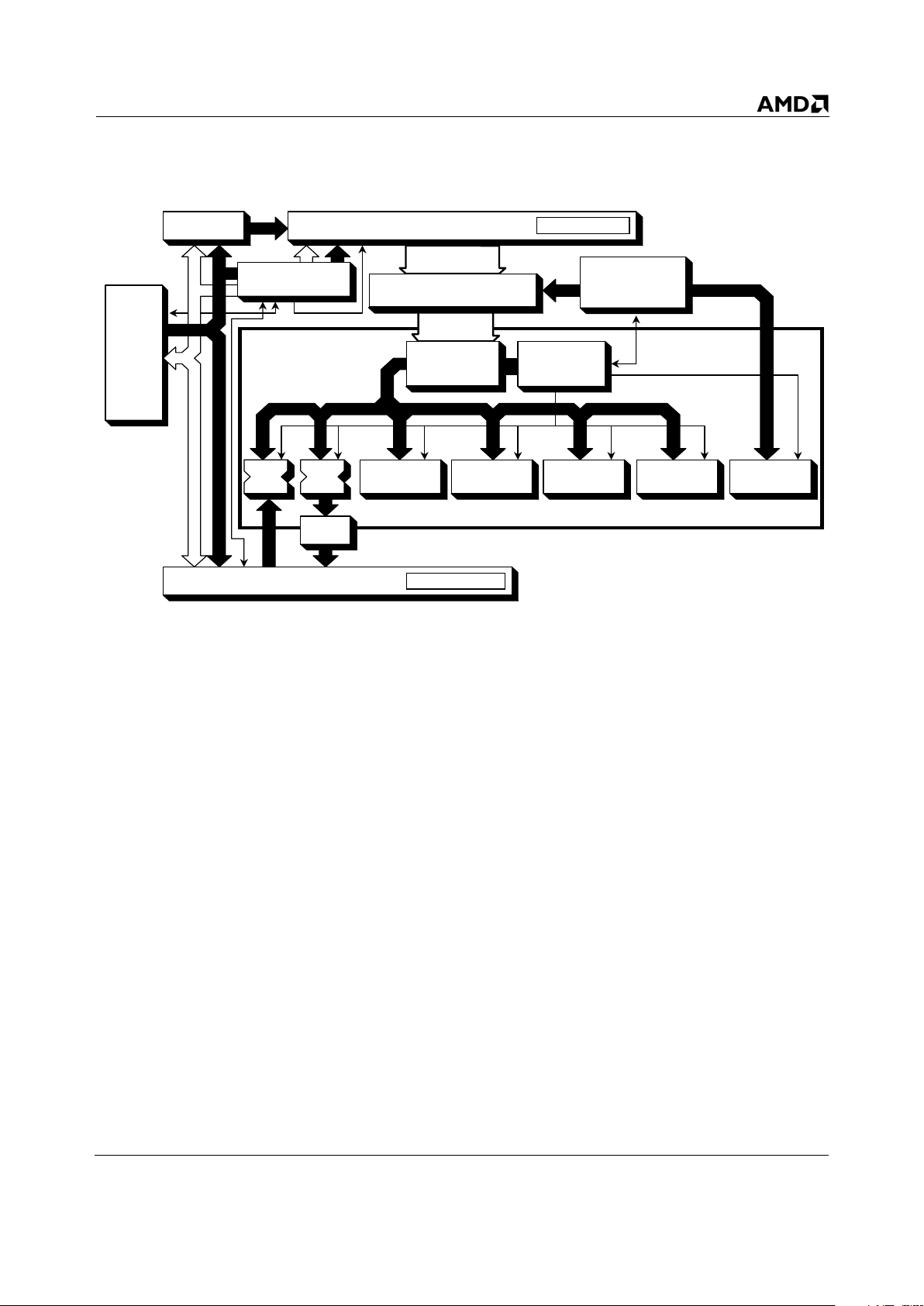
AMD-K6® Processor Block Diagram. As shown in Figure 1 on page 11,
the high-performance, out-of-order execution engine of the
AMD-K6 processor is mated to a split level-one 64-Kbyte
writeback cache with 32 Kbytes of instruction cache and 32
Kbytes of data cache. The instruction cache feeds the decoders
and, in turn, the decoders feed the scheduler. The ICU issues
and retires RISC86 operations contained in the scheduler. The
system bus interface is an industry-standard 64-bit Pentium
®
processor demultiplexed bus.
The AMD-K6 processor combines the latest in processor
microarchitecture to provide the highest x86 performance for
today’s personal computers. The AMD-K6 offers true
sixth-generation performance and full x86 binary software
compatibility.
Chapter 2 Internal Architecture 11
20695H/0—March 1998 AMD-K6
®
Processor Data Sheet
Preliminary Information
Figure 1. AMD-K6® Processor Block Diagram
2.3 Cache, Instruction Prefetch, and Predecode Bits
The writeback level-one cache on the AMD-K6 processor is
organized as a separate 32-Kbyte instruction cache and a
32-Kbyte data cache with two-way set associativity. The cache
line size is 32 bytes and lines are prefetched from main memory
using an efficient pipelined burst transaction. As the
instruction cache is filled, each instruction byte is analyzed for
instruction boundaries using predecoding logic. Predecoding
annotates each instruction byte with information that later
enables the decoders to efficiently decode multiple instructions
simultaneously.
Cache The processor cache design takes advantage of a sectored
organization (see Figure 2 on page 12). Each sector consists of
64 bytes configured as two 32-byte cache lines. The two cache
lines of a sector share a common tag but have separate pairs of
MESI (Modified, Exclusive, Shared, Invalid) bits that track the
state of each cache line.
Integer X
(Register) Unit
Store
Unit
Integer Y
(Register) Unit
Floating-Point
Unit
Branch
(Resolving) Unit
Store
Queue
Instruction
Control Unit
Scheduler
Buffer
(24 RISC86)
Six RISC86
®
Operation Issue
Out-of-Order
Execution Engine
Level-One Dual-Port Data Cache (32 KByte)
128-Entry DTLB
Level-One Instruction Cache
(32 KByte + Predecode)
64-Entry ITLB
Dual Instruction Decoders
x86 to RISC86
Branch Logic
(8192-Entry BHT)
(16-Entry BTC)
(16-Entry RAS)
Load
Unit
Multimedia
Unit
Predecode
Logic
Level-One Cache
Controller
Socket 7
Bus
Interface
16-Byte Fetch
Four RISC86
Decode

12 Internal Architecture Chapter 2
AMD-K6® Processor Data Sheet 20695H/0—March 1998
Preliminary Information
Figure 2. Cache Sector Organization
Two forms of cache misses and associated cache fills can take
place—a sector replacement and a cache line replacement. In
the case of a sector replacement, the miss is due to a tag
mismatch, in which case the required cache line is filled from
external memory, and the cache line within the sector that was
not required is marked as invalid. In the case of a cache line
replacement, the address matches the tag, but the requested
cache line is marked as invalid. The required cache line is filled
from external memory, and the cache line within the sector that
is not required remains in the same cache state.
Prefetching The AMD-K6 processor performs cache prefetching for sector
replacements only—as opposed to cache line replacements.
This cache prefetching results in the filling of the required
cache line first, and a prefetch of the second cache line.
Furthermore, the prefetch of the cache line that is not required
is initiated only in the forward direction—that is, only if the
requested cache line is the first cache line within the sector.
From the perspective of the external bus, the two cache-line
fills typically appear as two 32-byte burst read cycles occurring
back-to-back or, if allowed, as pipelined cycles.
Predecode Bits Decoding x86 instructions is particularly difficult because the
instructions are variable-length and can be from 1 to 15 bytes
long. Predecode logic supplies the predecode bits that are
associated with each instruction byte. The predecode bits
indicate the number of bytes to the start of the next x86
instruction. The predecode bits are stored in an extended
instruction cache alongside each x86 instruction byte as shown
in Figure 2 on page 12. The predecode bits are passed with the
instruction bytes to the decoders where they assist with parallel
x86 instruction decoding.
Tag
Address
Cache Line 1 Byte 31 Predecode Bits Byte 30 Predecode Bits ........ ........ Byte 0 Predecode Bits MESI Bits
Cache Line 2 Byte 31 Predecode Bits Byte 30 Predecode Bits ........ ........ Byte 0 Predecode Bits MESI Bits

Chapter 2 Internal Architecture 13
20695H/0—March 1998 AMD-K6
®
Processor Data Sheet
Preliminary Information
2.4 Instruction Fetch and Decode
Instruction Fetch The processor can fetch up to 16 bytes per clock out of the
instruction cache or branch target cache. The fetched
information is placed into a 16-byte instruction buffer that
feeds directly into the decoders (see Figure 3). Fetching can
occur along a single execution stream with up to seven
outstanding branches taken.
The instruction fetch logic is capable of retrieving any 16
contiguous bytes of information within a 32-byte boundary.
There is no additional penalty when the 16 bytes of instructions
lie across a cache line boundary. The instruction bytes are
loaded into the instruction buffer as they are consumed by the
decoders. Although instructions can be consumed with byte
granularity, the instruction buffer is managed on a
memory-aligned word (2 bytes) organization. Therefore,
instructions are loaded and replaced with word granularity.
When a control transfer occurs—such as a JMP instruction—
the entire instruction buffer is flushed and reloaded with a new
set of 16 instruction bytes.
Figure 3. The Instruction Buffer
16 Instruction Bytes
plus
16 Sets of Predecode Bits
Branch-Target Cache
16 x 16 B y te s
2:1
Instruction Buffer
16 Bytes
16 Bytes
Branch Target
Address Adders
Return Address Stack
16 x 16 Bytes
32-Kbyte Level-One
Instruction Cache
Fetch Unit

14 Internal Architecture Chapter 2
AMD-K6® Processor Data Sheet 20695H/0—March 1998
Preliminary Information
Instruction Decode The AMD-K6 processor decode logic is designed to decode
multiple x86 instructions per clock (see Figure 4). The decode
logic accepts x86 instruction bytes and their predecode bits
from the instruction buffer, locates the actual instruction
boundaries, and generates RISC86 operations from these x86
instructions.
RISC86 operations are fixed-format internal instructions. Most
RISC86 operations execute in a single clock. RISC86 operations
are combined to perform every function of the x86 instruction
set. Some x86 instructions are decoded into as few as zero
RISC86 opcodes—for instance a NOP—or one RISC86
operation—a register-to-register add. More complex x86
instructions are decoded into several RISC86 operations.
Figure 4. AMD-K6® Processor Decode Logic
Instruction Buffer
4 RISC86 Operations
On-Chip ROM
Long Decoder
Short Decoder #1
Short Decoder #2
Vector Address
Vector Decoder
RISC86® Sequencer

Chapter 2 Internal Architecture 15
20695H/0—March 1998 AMD-K6
®
Processor Data Sheet
Preliminary Information
The AMD-K6 processor uses a combination of decoders to
convert x86 instructions into RISC86 operations. The hardware
consists of three sets of decoders—two parallel short decoders,
one long decoder, and one vectoring decoder. The parallel short
decoders translate the most commonly-used x86 instructions
(moves, shifts, branches, ALU, MMX, FPU) into zero, one, or
two RISC86 operations each. The short decoders only operate
on x86 instructions that are up to seven bytes long. In addition,
they are designed to decode up to two x86 instructions per
clock. The commonly-used x86 instructions that are greater
than seven bytes but not more than 11 bytes long, and
semi-commonly-used x86 instructions that are up to seven bytes
long are handled by the long decoder.
The long decoder only performs one decode per clock and
generates up to four RISC86 operations. All other translations
(complex instructions, serializing conditions, interrupts and
exceptions, etc.) are handled by a combination of the vector
decoder and RISC86 operation sequences fetched from an
on-chip ROM. For complex operations, the vector decoder logic
provides the first set of RISC86 operations and a vector (initial
ROM address) to a sequence of further RISC86 operations. The
same types of RISC86 operations are fetched from the ROM as
those that are generated by the hardware decoders.
Note: Although all three sets of decoders are simultaneously fed a
copy of the instruction buffer contents, only one of the three
types of decoders is used during any one decode clock.
The decoders or the RISC86 sequencer always generate a group
of four RISC86 operations. For decodes that cannot fill the entire
group with four RISC86 operations, RISC86 NOP operations are
placed in the empty locations of the grouping. For example, a
long-decoded x86 instruction that converts to only three RISC86
operations is padded with a single RISC86 NOP operation and
then passed to the scheduler. Up to six groups or 24 RISC86
operations can be placed in the scheduler at a time.
All of the common, and a few of the uncommon, floating-point
instructions (also known as ESC instructions) are hardware
decoded as short decodes. This decode generates a RISC86
floating-point operation and, optionally, an associated
floating-point load or store operation. Floating-point or ESC
instruction decode is only allowed in the first short decoder, but
non-ESC instructions, excluding MMX instructions, can be

16 Internal Architecture Chapter 2
AMD-K6® Processor Data Sheet 20695H/0—March 1998
Preliminary Information
decoded simultaneously by the second short decoder along with
an ESC instruction decode in the first short decoder.
All of the MMX instructions, with the exception of the EMMS
instruction, are hardware decoded as short decodes. The MMX
instruction decode generates a RISC86 MMX operation and,
optionally, an associated MMX load or store operation. MMX
instruction decode is only allowed in the first short decoder.
However, instructions other than MMX and ESC instructions
can be decoded simultaneously by the second short decoder
along with an MMX instruction decode in the first short
decoder.
2.5 Centralized Scheduler
The scheduler is the heart of the AMD-K6 processor (see Figure
5 on page 17). It contains the logic necessary to manage
out-of-order execution, data forwarding, register renaming,
simultaneous issue and retirement of multiple RISC86
operations, and speculative execution. The scheduler’s buffer
can hold up to 24 RISC86 operations. This equates to a maximum
of 12 x86 instructions. When possible, the scheduler can
simultaneously issue a RISC86 operation to any available
execution unit (store, load, branch, integer, integer/multimedia,
or floating-point). In total, the scheduler can issue up to six and
retire up to four RISC86 operations per clock.
The main advantage of the scheduler and its operation buffer is
the ability to examine an x86 instruction window equal to 12
x86 instructions at one time. This advantage is due to the fact
that the scheduler operates on the RISC86 operations in
parallel and allows the AMD-K6 processor to perform dynamic
on-the-fly instruction code scheduling for optimized execution.
Although the scheduler can issue RISC86 operations for
out-of-order execution, it always retires x86 instructions in
order.

Chapter 2 Internal Architecture 17
20695H/0—March 1998 AMD-K6
®
Processor Data Sheet
Preliminary Information
Figure 5. AMD-K6® Processor Scheduler
2.6 Execution Units
The AMD-K6 processor contains seven execution units—store,
load, integer X, integer Y, multimedia, floating-point, and
branch condition. Each unit is independent and capable of
handling the RISC86 operations. Table 1 on page 18 details the
execution units, functions performed within these units,
operation latency, and operation throughput.
The store and load execution units are two-staged pipelined
designs. The store unit performs data writes and register
calculation for LEA/PUSH. Data memory and register writes
from stores are available after one clock. The load unit
performs data memory reads. Data is available from the load
unit after two clocks.
The Integer X execution unit can operate on all ALU
operations, multiplies, divides (signed and unsigned), shifts,
and rotates.
RISC86 Operation Buffer
RISC86 Issue Buses
RISC86 #0
RISC86 #1
RISC86 #2
RISC86 #3
Centralized RISC86
®
Operation Scheduler
From Decode Logic

18 Internal Architecture Chapter 2
AMD-K6® Processor Data Sheet 20695H/0—March 1998
Preliminary Information
The multimedia unit shares pipeline control with the Integer X
unit and executes all MMX instructions.
The Integer Y execution unit can operate on the basic word and
doubleword ALU operations—ADD, AND, CMP, OR, SUB,
XOR, zero-extend and sign-extend operands.
The branch condition unit is separate from the branch
prediction logic in that it resolves conditional branches such as
JCC and LOOP after the branch condition has been evaluated.
Table 1. Execution Latency and Throughput of Execution Units
Execution Unit Function Latency Throughput
Store
LEA/PUSH, Address 1 1
Memory Store 1 1
Load Memory Loads 2 1
Integer X
Integer ALU 1 1
Integer Multiply 2–3 2–3
Integer Shift 1 1
Multimedia
MMX ALU 1 1
MMX Shifts, Packs, Unpack 1 1
MMX Multiply 1–2 1–2
Integer Y
Basic ALU (16
- & 32-bit operands)
11
Branch Resolves Branch Conditions 1 1
FPU FADD, FSUB, FMUL 2 2

Chapter 2 Internal Architecture 19
20695H/0—March 1998 AMD-K6
®
Processor Data Sheet
Preliminary Information
2.7 Branch-Prediction Logic
Sophisticated branch logic that can minimize or hide the impact
of changes in program flow is designed into the AMD-K6
processor. Branches in x86 code fit into two categories—
unconditional branches, which always change program flow (that
is, the branches are always taken) and conditional branches,
which may or may not divert program flow (that is, the branches
are taken or not-taken). When a conditional branch is not taken,
the processor simply continues decoding and executing the next
instructions in memory.
Typical applications have up to 10% of unconditional branches
and another 10% to 20% conditional branches. The AMD-K6
branch logic has been designed to handle this type of program
behavior and its negative effects on instruction execution, such
as stalls due to delayed instruction fetching and the draining of
the processor pipeline. The branch logic contains an 8192-entry
branch history table, a 16-entry by 16-byte branch target cache,
a 16-entry return address stack, and a branch execution unit.
Branch History Table The AMD-K6 processor handles unconditional branches
without any penalty by redirecting instruction fetching to the
target address of the unconditional branch. However,
conditional branches require the use of the dynamic
branch-prediction mechanism built into the AMD-K6. A
two-level adaptive history algorithm is implemented in an
8192-entry branch history table. This table stores executed
branch information, predicts individual branches, and predicts
the behavior of groups of branches. To accommodate the large
branch history table, the AMD-K6 processor does not store
predicted target addresses. Instead, the branch target
addresses are calculated on-the-fly using ALUs during the
decode stage. The adders calculate all possible target addresses
before the instructions are fully decoded and the processor
chooses which addresses are valid.
Branch Target Cache To avoid a one clock cache-fetch penalty when a branch is
predicted taken, a built-in branch target cache supplies the first
16 bytes of instructions directly to the instruction buffer
(assuming the target address hits this cache). (See Figure 3 on
page 13.) The branch target cache is organized as 16 entries of
16 bytes. In total, the branch prediction logic achieves branch
prediction rates greater than 95%.

20 Internal Architecture Chapter 2
AMD-K6® Processor Data Sheet 20695H/0—March 1998
Preliminary Information
Return Address Stack The return address stack is a special device designed to
optimize CALL and RET pairs. Software is typically compiled
with subroutines that are frequently called from various places
in a program. This is usually done to save space. Entry into the
subroutine occurs with the execution of a CALL instruction. At
that time, the processor pushes the address of the next
instruction in memory following the CALL instruction onto the
stack (allocated space in memory). When the processor
encounters a RET instruction (within or at the end of the
subroutine), the branch logic pops the address from the stack
and begins fetching from that location. To avoid the latency of
main memory accesses during CALL and RET operations, the
return address stack caches the pushed addresses.
Branch Execution
Unit
The branch execution unit enables efficient speculative
execution. This unit gives the processor the ability to execute
instructions beyond conditional branches before knowing
whether the branch prediction was correct. The AMD-K6
processor does not permanently update the x86 registers or
memory locations until all speculatively executed conditional
branch instructions are resolved. When a prediction is
incorrect, the processor backs out to the point of the
mispredicted branch instruction and restores all registers. The
AMD-K6 can support up to seven outstanding branches.

Chapter 3 Software Environment 21
20695H/0—March 1998 AMD-K6
®
Processor Data Sheet
Preliminary Information
3 Software Environment
This chapter provides a general overview of the AMD-K6
processor’s x86 software environment and briefly describes the
data types, registers, operating modes, interrupts, and
instructions supported by the AMD-K6 architecture and design
implementation.
3.1 Registers
The AMD-K6 processor contains all the registers defined by the
x86 architecture, including general-purpose, segment,
floating-point, MMX, EFLAGS, control, task, debug, test, and
descriptor/memory-management registers. In addition, this
chapter provides information on the AMD-K6 Model-Specific
Registers (MSRs).
Note: Areas of the register designated as Reserved should not be
modified by software.
General-Purpose
Registers
The eight 32-bit x86 general-purpose registers are used to hold
integer data or memory pointers used by instructions. Table 2
contains a list of the general-purpose registers and the
functions for which they are used.
In order to support byte and word operations, EAX, EBX, ECX,
and EDX can also be used as 8-bit and 16-bit registers. The
shorter registers are overlaid on the longer ones. For example,
the name of the 16-bit version of EAX is AX (low 16 bits of
EAX) and the 8-bit names for AX are AH (high order bits) and
Table 2. General-Purpose Registers
Register Function
EAX Commonly used as an accumulator
EBX Commonly used as a pointer
ECX Commonly used for counting in loop operations
EDX Commonly used to hold I/O information and to pass parameters
EDI Commonly used as a destination pointer by the ES segment
ESI Commonly used as a source pointer by the DS segment
ESP Used to point to the stack segment
EBP Used to point to data within the stack segment

22 Software Environment Chapter 3
AMD-K6® Processor Data Sheet 20695H/0—March 1998
Preliminary Information
AL (low order bits). The same naming convention applies to
EBX, ECX, and EDX. EDI, ESI, ESP, and EBP can be used as
smaller 16-bit registers called DI, SI, SP, and BP respectively,
but these registers do not have 8-bit versions. Figure 6 shows the
EAX register with its name components, and Table 3 lists the
dword (32 bits) general-purpose registers and their
corresponding word (16 bits) and byte (8 bits) versions.
Figure 6. EAX Register with 16-Bit and 8-Bit Name Components
87 0151631
EAX
AX
AH
AL
Table 3. General-Purpose Register Dword, Word, and Byte Names
32-Bit Name
(Dword)
16-Bit Name
(Word)
8-Bit Name
(High-order Bits)
8-Bit Name
(Low-order Bits)
EAX AX AH AL
EBX BX BH BL
ECX CX CH CL
EDX DX DH DL
EDI DI ––
ESI SI – –
ESP SP – –
EBP BP – –

Chapter 3 Software Environment 23
20695H/0—March 1998 AMD-K6
®
Processor Data Sheet
Preliminary Information
Integer Data Types Four types of data are used in general-purpose registers—byte,
word, doubleword, and quadword integers. Figure 7 shows the
format of the integer data registers.
Figure 7. Integer Data Types
15 0
31 0
Precision — 32 Bits
Precision — 16 Bits
Word Integer
Doubleword Integer
70
Precision —
8 Bits
Byte Integer
63 0
Precision — 64 Bits
Quadword Integer

24 Software Environment Chapter 3
AMD-K6® Processor Data Sheet 20695H/0—March 1998
Preliminary Information
Segment Registers The six 16-bit segment registers are used as pointers to areas
(segments) of memory. Table 4 lists the segment registers and
their functions. Figure 8 shows the format for all six segment
registers.
Figure 8. Segment Register
Segment Usage The operating system determines the type of memory model
that is implemented. The segment register usage is determined
by the operating system’s memory model. In a Real mode
memory model the segment register points to the base address
in memory. In a Protected mode memory model the segment
register is called a selector and it selects a segment descriptor
in a descriptor table. This descriptor contains a pointer to the
base of the segment, the limit of the segment, and various
protection attributes. For more information on descriptor
formats, see “Descriptors and Gates” on page 45. Figure 9 on
page 25 shows segment usage for Real mode and Protected
mode memory models.
Table 4. Segment Registers
Segment
Register
Segment Register Function
CS Code segment, where instructions are located
DS Data segment, where data is located
ES Data segment, where data is located
FS Data segment, where data is located
GS Data segment, where data is located
SS Stack segment
015

Chapter 3 Software Environment 25
20695H/0—March 1998 AMD-K6
®
Processor Data Sheet
Preliminary Information
Figure 9. Segment Usage
Instruction Pointer The instruction pointer (EIP or IP) is used in conjunction with
the code segment register (CS). The instruction pointer is
either a 32-bit register (EIP) or a 16-bit register (IP) that keeps
track of where the next instruction resides within memory. This
register cannot be directly manipulated, but can be altered by
modifying return pointers when a JMP or CALL instruction is
used.
Floating-Point
Registers
The floating-point execution unit in the AMD-K6 processor is
designed to perform mathematical operations on non-integer
numbers. This floating-point unit conforms to the IEEE 754 and
854 standards and uses several registers to meet these
standards—eight numeric floating-point registers, a status
word register, a control word register, and a tag word register.
Segment Register
Real Mode Memory Model
Segment Selector
Physical Memory
Protected Mode Memory Model
Base
Descriptor Table
Physical Memory
Segment Base
Base
Limit
BaseLimit
Segment Base

26 Software Environment Chapter 3
AMD-K6® Processor Data Sheet 20695H/0—March 1998
Preliminary Information
The eight floating-point registers are 80 bits wide and labeled
FPR0–FPR7. Figure 10 shows the format of these floating-point
registers. See “Floating-Point Register Data Types” on page 28
for information on allowable floating-point data types.
Figure 10. Floating-Point Register
The 16-bit FPU status word register contains information about
the state of the floating-point unit. Figure 11 shows the format
of this register.
Figure 11. FPU Status Word Register
64 63 07879
Sign Exponent Significand
9876543210101112131415
P
E
O
E
ESC0C
1
I
E
Z
E
U
E
S
F
TOSP
C
3
B
C
2
D
E
Symbol Description Bits
B FPU Busy 15
C3 Condition Code 14
TOSP Top of Stack Pointer 13–11
C2 Condition Code 10
C1 Condition Code 9
C0 Condition Code 8
ES Error Summary Status 7
SF Stack Fault 6
Exception Flags
PE Precision Error 5
UE Underflow Error 4
OE Overflow Error 3
ZE Zero Divide Error 2
DE Denormalized Operation Error 1
IE Invalid Operation Error 0
TOSP Information
000 = FPR0
111 = F PR7

Chapter 3 Software Environment 27
20695H/0—March 1998 AMD-K6
®
Processor Data Sheet
Preliminary Information
The FPU control word register allows a programmer to manage
the FPU processing options. Figure 12 shows the format of this
register.
Figure 12. FPU Control Word Register
The FPU tag word register contains information about the
registers in the register stack. Figure 13 shows the format of this
register.
Figure 13. FPU Tag Word Register
Symbol Description Bits
Y Infinity Bit (80287 compatibility) 12
RC Rounding Control 11–10
PC Precision Control 9–8
Exception Masks
PM Precision 5
UM Underflow 4
OM Overflow 3
ZM Zero Divide 2
DM Denormalized Operation 1
IM Invalid Operation 0
9876543210101112131415
P
M
O
M
P
C
R
C
I
M
Z
M
U
M
D
M
Rounding Control Information
00b = Round to the nearest or even number
01b = Round down toward negative infinity
10b = Round up toward positive infinity
11b = Truncate toward zero
Reserved
Y
Precision Control Information
00b = 24 bits Single Precision Real
01b = Reserved
10b = 53 bits Double Precision Real
11b = 64 bits Extended Precision Real
9876543210101112131415
TAG
(FPR6
TAG
(FPR7
TAG
(FPR4
TAG
(FPR5
TAG
(FPR2
TAG
(FPR3
TAG
(FPR0
TAG
(FPR1
Tag Values
00 = Valid
01 = Zero
10 = Special
11 = Empt y

28 Software Environment Chapter 3
AMD-K6® Processor Data Sheet 20695H/0—March 1998
Preliminary Information
Floating-Point
Register Data Types
Floating-point registers use four different types of data—
packed decimal, single precision real, double precision real,
and extended precision real. Figures 14 and 15 show the
formats for these registers.
Figure 14. Packed Decimal Data Type
Figure 15. Precision Real Data Types
079
Precision — 18 Digits, 72 Bits Used, 4-Bits/Digit
71
S
Ignore
or
Zero
Description Bits
Ignored on Load, Zeros on Store 78-72
Sign Bit 79
78 72
063
Double Precision Real
31 0
Single Precision Real
079
22
S
Biased
Exponent
78
23
S
Biased
Exponent
6364
5152
Biased
Exponent
S
Significand
Significand
Significand
30
62
Extended Precision Real
S = Sign Bit
S = Sign Bit
S = Sign Bit
I
62
I = Integer Bit

Chapter 3 Software Environment 29
20695H/0—March 1998 AMD-K6
®
Processor Data Sheet
Preliminary Information
MMX™ Registers The AMD-K6 processor implements eight 64-bit MMX registers
and three packed data types for use by multimedia software.
These registers are mapped on the floating-point registers. The
MMX instructions refer to these registers as mm0 to mm7.
Figures 16 and 17 show the format of these registers and data
types. See AMD-K6® Processor Multimedia Technology, order#
20726 for more information.
Figure 16. MMX™ Registers
63 0
mm0
mm7
mm1
mm6
mm5
mm2
mm3
mm4

30 Software Environment Chapter 3
AMD-K6® Processor Data Sheet 20695H/0—March 1998
Preliminary Information
Figure 17. MMX™ Data Types
63 0
Packed Bytes
63 0
Packed Words
63 0
Packed Doublewords
32 31
48 47 32 31 16 15
56 55 48 47 40 39 32 31 24 23 16 15 8 7

Chapter 3 Software Environment 31
20695H/0—March 1998 AMD-K6
®
Processor Data Sheet
Preliminary Information
EFLAGS Register The EFLAGS register provides for three different types of
flags—system, control, and status. The system flags provide
operating system controls, the control flag provides directional
information for string operations, and the status flags provide
information resulting from logical and arithmetic operations.
Figure 18 shows the format of this register.
Figure 18. EFLAGS Registers
9876543210101112131415161718192021
I
O
P
L
31 30 29 28 27 26 25 24 23 22
A
F
P
F
ZFS
F
IFD
F
T
F
O
F
N
T
RFVMA
C
V
I
F
V
I
P
I
D
C
F
Reserved
Symbol Description Bits
ID ID Flag 21
VIP Virtual Interrupt Pending 20
VIF Virtual Interrupt Flag 19
AC Alignment Check 18
VM Virtual-8086 Mode 17
RF Resume Flag 16
NT Nested Task 14
IOPL I/O Privilege Level 13–12
OF Overflow Flag 11
DF Direction Flag 10
IF Interrupt Flag 9
TF Trap Flag 8
SF Sign Flag 7
ZF Zero Flag 6
AF Auxiliary Flag 4
PF Parity Flag 2
CF Carry Flag 0

32 Software Environment Chapter 3
AMD-K6® Processor Data Sheet 20695H/0—March 1998
Preliminary Information
Control Registers The five control registers contain system control bits and
pointers. Figures 19 through 23 show the formats of these
registers.
Figure 19. Control Register 4 (CR4)
Figure 20. Control Register 3 (CR3)
Figure 21. Control Register 2 (CR2)
7654321031
P
S
E
T
S
D
M
C
E
V
M
E
D
E
P
V
I
Reserved
Symbol Description Bit
MCE Machine Check Enable 6
PSE Page Size Extensions 4
DE Debugging Extensions 3
TSD Time Stamp Disable 2
PVI Protected Virtual Interrupts 1
VME Virtual-8086 Mode Extensions 0
P
C
D
Reserved
987654321010111213141516171819202131 30 29 28 27 26 25 24 23 22
Page Directory Base
Symbol Description Bit
PCD Page Cache Disable 4
PWT Page Writethrough 3
P
W
T
031
Page Fault Linear Address

Chapter 3 Software Environment 33
20695H/0—March 1998 AMD-K6
®
Processor Data Sheet
Preliminary Information
Figure 22. Control Register 1 (CR1)
Figure 23. Control Register 0 (CR0)
031
Reserved
ETT
S
Reserved
987654321010111213141516171819202131 30 29 28 27 26 25 24 23 22
A
M
E
M
W
P
MPP
E
N
E
PGCDN
W
Symbol Description Bit
PG Paging 31
CD Cache Disable 30
NW Not Writethrough 29
Symbol Description Bit
AM Alignment Mask 18
WP Write Protect 16
NE Numeric Error 5
ET Extension Type 4
TS Task Switched 3
EM Emulation 2
MP Monitor Co-processor 1
PE Protection Enabled 0

34 Software Environment Chapter 3
AMD-K6® Processor Data Sheet 20695H/0—March 1998
Preliminary Information
Debug Registers Figures 24 through 27 show the 32-bit debug registers
supported by the processor.
Figure 24. Debug Register DR7
Symbol Description Bit
GD General Detect Enabled 13
GE Global Exact Breakpoint Enabled 9
LE Local Exact Breakpoint Enabled 8
G3 Global Exact Breakpoint # 3 Enabled 7
L3 Local Exact Breakpoint # 3 Enabled 6
G2 Global Exact Breakpoint # 2 Enabled 5
L2 Local Exact Breakpoint # 2 Enabled 4
G1 Global Exact Breakpoint # 1 Enabled 3
L1 Local Exact Breakpoint # 1 Enabled 2
G0 Global Exact Breakpoint # 0 Enabled 1
L0 Local Exact Breakpoint # 0 Enabled 0
9876543210101112131415
L
2
L
1
L3G
3
GEL
E
L
0
Reserved
G
0
G
1
L
2
G
D
25 24 23 22 21 20 19 18 17 16262728293031
R/W
3
LEN
3
R/W
2
LEN
2
R/W
1
LEN
1
R/W
0
LEN
0
Symbol Description Bits
LEN 3 Length of Breakpoint #3 31–30
R/W 3 Type of Transaction(s) to Trap 29–28
LEN 2 Length of Breakpoint #2 27–26
R/W 2 Type of Transaction(s) to Trap 25–24
LEN 1 Length of Breakpoint #1 23–22
R/W 1 Type of Transaction(s) to Trap 21–20
LEN 0 Length of Breakpoint #0 19–18
R/W 0 Type of Transaction(s) to Trap 17–16

Chapter 3 Software Environment 35
20695H/0—March 1998 AMD-K6
®
Processor Data Sheet
Preliminary Information
Figure 25. Debug Register DR6
Figure 26. Debug Registers DR5 and DR4
987654321010111213141516171819202131 30 29 28 27 26 25 24 23 22
B
1
B
2
B
S
B
0
Reserved
B
T
B
D
Symbol Description Bit
BT Breakpoint Task Switch 15
BS Breakpoint Single Step 14
BD Breakpoint Debug Access Detected 13
B3 Breakpoint #3 Condition Detected 3
B2 Breakpoint #2 Condition Detected 2
B1 Breakpoint #1 Condition Detected 1
B0 Breakpoint #0 Condition Detected 0
B
3
987654321010111213141516171819202131 30 29 28 27 26 25 24 23 22
Reserved
DR5
987654321010111213141516171819202131 30 29 28 27 26 25 24 23 22
Reserved
DR4

36 Software Environment Chapter 3
AMD-K6® Processor Data Sheet 20695H/0—March 1998
Preliminary Information
Figure 27. Debug Registers DR3, DR2, DR1, and DR0
987654321010111213141516171819202131 30 29 28 27 26 25 24 23 22
Breakpoint 3 32-bit Linear Address
DR3
987654321010111213141516171819202131 30 29 28 27 26 25 24 23 22
Breakpoint 0 32-bit Linear Address
DR0
987654321010111213141516171819202131 30 29 28 27 26 25 24 23 22
Breakpoint 2 32-bit Linear Address
DR2
987654321010111213141516171819202131 30 29 28 27 26 25 24 23 22
Breakpoint 1 32-bit Linear Address
DR1

Chapter 3 Software Environment 37
20695H/0—March 1998 AMD-K6
®
Processor Data Sheet
Preliminary Information
Model-Specific
Registers (MSR)
The AMD-K6 processor provides five MSRs. The value in the
ECX register selects the MSR to be addressed by the RDMSR
and WRMSR instructions. The values in EAX and EDX are used
as inputs and outputs by the RDMSR and WRMSR instructions.
Table 5 lists the MSRs and the corresponding value of the ECX
register. Figures 28 through 32 show the MSR formats.
For more information about the RDMSR and WRMSR
instructions, see the AMD K86™ Family BIOS and Software Tools
Development Guide, order# 21062.
MCAR and MCTR. The AMD-K6 processor does not support the
generation of a machine check exception. However, the
processor does provide a 64-bit Machine Check Address
Register (MCAR), a 64-bit Machine Check Type Register
(MCTR), and a Machine Check Enable (MCE) bit in CR4.
Because the processor does not support machine check
exceptions, the contents of the MCAR and MCTR are only
affected by the WRMSR instruction and by RESET being
sampled asserted (where all bits in each register are reset to 0).
Figure 28. Machine-Check Address Register (MCAR)
Table 5. Model-Specific Registers (MSRs)
Model-Specific Register Value of ECX
Machine Check Address Register (MCAR) 00h
Machine Check Type Register (MCTR) 01h
Test Register 12 (TR12) 0Eh
Time Stamp Counter (TSC) 10h
Write Handling Control Register (WHCR) C000_0082h
0
63
MCAR

38 Software Environment Chapter 3
AMD-K6® Processor Data Sheet 20695H/0—March 1998
Preliminary Information
Figure 29. Machine-Check Type Register (MCTR)
Test Register 12 (TR12). Test register 12 provides a method for
disabling the L1 caches. Figure 30 shows the format of TR12.
Figure 30. Test Register 12 (TR12)
Time Stamp Counter. With each processor clock cycle, the
processor increments the 64-bit time stamp counter (TSC) MSR.
Figure 31 shows the format of the TSC.
Figure 31. Time Stamp Counter (TSC)
54 063
Reserved
MCTR
Reserved
421063
C
I
3
Symbol Description Bit
CI Cache Inhibit Bit 3
063
TSC

Chapter 3 Software Environment 39
20695H/0—March 1998 AMD-K6
®
Processor Data Sheet
Preliminary Information
Write Handling Control Register (WHCR). The Write Handling Control
Register (WHCR) is a MSR that contains three fields—the
WCDE bit, Write Allocate Enable Limit (WAELIM) field, and
the Write Allocate Enable 15-to-16-Mbyte (WAE15M) bit.
Figure 32 shows the format of WHCR. See “Write Allocate” on
page 177 for more information.
Figure 32. Write Handling Control Register (WHCR)
Memory
Management
Registers
The AMD-K6 processor controls segmented memory
management with the registers listed in Table 6. Figure 33 on
page 40 shows the formats of these registers.
71063
Reserved
WAELIM
8
0
Note: Hardware RESET initializes this MSR to all zeros.
W
A
E
1
5
M
Symbol Description Bits
WCDE Always program to 0 8
WAELIM Write Allocate Enable Limit 7–1
WAE15M Write Allocate Enable 15-to-16-Mbyte 0
9
Table 6. Memory Management Registers
Register Name Function
Global Descriptor Table Register Contains a pointer to the base of the Global Descriptor Table
Interrupt Descriptor Table Register Contains a pointer to the base of the Interrupt Descriptor Table
Local Descriptor Table Register Contains a pointer to the Local Descriptor Table of the current task
Task Register Contains a pointer to the Task State Segment of the current task

40 Software Environment Chapter 3
AMD-K6® Processor Data Sheet 20695H/0—March 1998
Preliminary Information
Figure 33. Memory Management Registers
15 0
16-Bit Limit
16
47
32-Bit Linear Base Address
Global and Interrupt Descriptor Table Registers
31
063
32-Bit Limit
32
32-Bit Linear Base Address
15 0
Local Descriptor Table Register and Task Register
Attributes
15 0
Selector

Chapter 3 Software Environment 41
20695H/0—March 1998 AMD-K6
®
Processor Data Sheet
Preliminary Information
Task State Segment Figure 34 shows the format of the Task State Segment (TSS).
Figure 34. Task State Segment (TSS)
31
Interrupt Redirection Bitmap (IRB)
(eight 32-bit locations)
0
I/O Permission Bitmap (IOPB)
(up to 8 Kbytes)
Operating System
Data Structure
Base Address of IOPB
LDT Selector
0000h
0000h
0000h
0000h
0000h
0000h
0000h
GS
FS
DS
SS
CS
ES
EDI
ESI
EBP
ESP
EBX
EDX
ECX
EAX
CR3
EFLAGS
EIP
0000h
0000h
0000h
0000h
SS2
SS1
SS0
Link (Prior TSS Selector)
ESP0
ESP1
ESP2
TSS Limit
from TR
64h
0
T
0000h

42 Software Environment Chapter 3
AMD-K6® Processor Data Sheet 20695H/0—March 1998
Preliminary Information
Paging The AMD-K6 processor can address up to 4 Gbytes of memory.
This memory can be segmented into pages. The size of these
pages is determined by the operating system design and the
values set up in the Page Directory Entries (PDE) and Page
Table Entries (PTE). The processor can access both 4-Kbyte
pages and 4-Mbyte pages, and the page sizes can be intermixed
within a page directory. When the Page Size Extension (PSE)
bit in CR4 is set, the processor translates linear addresses using
either the 4-Kbyte Translation Lookaside Buffer (TLB) or the
4-Mbyte TLB, depending on the state of the page size (PS) bit in
the page directory entry. Figures 35 and 36 show how 4-Kbyte
and 4-Mbyte page translations work.
Figure 35. 4-Kbyte Paging Mechanism
Linear Address
Page
Directory
Page
Tab le
4-Kbyte
Page
Frame
CR3
011122131 22
Page Directory
Offset
Page Table
Offset
Page
Offset
PDE
PTE
Physical
Address

Chapter 3 Software Environment 43
20695H/0—March 1998 AMD-K6
®
Processor Data Sheet
Preliminary Information
Figure 36. 4-Mbyte Paging Mechanism
Figures 37 through 39 show the formats of the PDE and PTE.
These entries contain information regarding the location of
pages and their status.
Linear Address
Page
Directory
4-Mbyte
Page
Frame
CR3
02131 22
Page Directory
Offset
Page
Offset
PDE
Physical
Address

44 Software Environment Chapter 3
AMD-K6® Processor Data Sheet 20695H/0—March 1998
Preliminary Information
Figure 37. Page Directory Entry 4-Kbyte Page Table (PDE)
Figure 38. Page Directory Entry 4-Mbyte Page Table (PDE)
876543210
31
P
C
D
U
/
S
W
/
R
9101112
A
V
L
0 A
P
W
T
P
Page Table Base Address
Symbol Description Bits
AVL Available to Software 11–9
Reserved 8
PS Page Size 7
Reserved 6
A Accessed 5
PCD Page Cache Disable 4
PWT Page Writethrough 3
U/S User/Supervisor 2
W/R Write/Read 1
P Present (valid) 0
876543210
31
P
C
D
U
/
S
W
/
R
9101112
A
V
L
1 A
P
W
T
P
Physical Page Base Address Reserved
2122
Symbol Description Bits
AVL Available to Software 11–9
Reserved 8
PS Page Size 7
Reserved 6
A Accessed 5
PCD Page Cache Disable 4
PWT Page Writethrough 3
U/S User/Supervisor 2
W/R Write/Read 1
P Present (valid) 0

Chapter 3 Software Environment 45
20695H/0—March 1998 AMD-K6
®
Processor Data Sheet
Preliminary Information
Figure 39. Page Table Entry (PTE)
Descriptors and Gates There are various types of structures and registers in the x86
architecture that define, protect, and isolate code segments,
data segments, task state segments, and gates. These structures
are called descriptors.
Figure 40 on page 46 shows the application segment descriptor
format. Table 7 contains information describing the memory
segment type to which the descriptor points. The application
segment descriptor is used to point to either a data or code
segment.
Figure 41 on page 47 shows the system segment descriptor
format. Table 8 contains information describing the type of
segment or gate to which the descriptor points. The system
segment descriptor is used to point to a task state segment, a
call gate, or a local descriptor table.
The AMD-K6 processor uses gates to transfer control between
executable segments with different privilege levels. Figure 42
on page 48 shows the format of the gate descriptor types. Table
8 contains information describing the type of segment or gate
to which the descriptor points.
876543210
31
P
C
D
U
/
S
W
/
R
9101112
A
V
L
A
P
W
T
P
Physical Page Base Address
Symbol Description Bits
AVL Available to Software 11–9
Reserved 8–7
D Dirty 6
A Accessed 5
PCD Page Cache Disable 4
PWT Page Writethrough 3
U/S User/Supervisor 2
W/R Write/Read 1
P Present (valid) 0
D

46 Software Environment Chapter 3
AMD-K6® Processor Data Sheet 20695H/0—March 1998
Preliminary Information
Figure 40. Application Segment Descriptor
Base Address 15–0 Segment Limit 15–0
987654321010111213141516171819202131 30 29 28 27 26 25 24 23 22
Segment
Limit
P DPL 1 Ty pe
A
V
L
G DBase Address 31–24 Base Address 23–16
Symbol Description Bits
G Granularity 23
D 32-Bit/16-Bit 22
AVL Available to Software 20
P Present/Valid Bit 15
DPL Descriptor Privilege Level 14-13
DT Descriptor Type 12
Type See Table 7 11-8
Reserved
Table 7. Application Segment Types
Type Data/Code Description
0
Data
Read-Only
1 Read-Only—Accessed
2 Read/Write
3 Read/Write—Accessed
4 Read-Only—Expand-down
5 Read-Only—Expand-down, Accessed
6 Read/Write—Expand-down
7 Read/Write—Expand-down, Accessed
8
Code
Execute-Only
9 Execute-Only—Accessed
A Execute/Read
B Execute/Read—Accessed
C Execute-Only—Conforming
D Execute-Only—Conforming, Accessed
E Execute/Read-Only—Conforming
F Execute/Read-Only—Conforming, Accessed

Chapter 3 Software Environment 47
20695H/0—March 1998 AMD-K6
®
Processor Data Sheet
Preliminary Information
Figure 41. System Segment Descriptor
Base Address 15–0 Segment Limit 15–0
987654321010111213141516171819202131 30 29 28 27 26 25 24 23 22
Segment
Limit
P DPL 0 Ty pe
A
V
L
G XBase Address 31–24 Base Address 23–16
Symbol Description Bits
G Granularity 23
X Not Needed 22
AVL Availability to Software 20
P Present/Valid Bit 15
DPL Descriptor Privilege Level 14-13
DT Descriptor Type 12
Type See Table 8 11-8
Reserved
Table 8. System Segment and Gate Types
Type Description
0 Reserved
1 Available 16-bit TSS
2LDT
3 Busy 16-bit TSS
4 16-bit Call Gate
5 Task Gate
6 16-bit Interrupt Gate
7 16-bit Trap Gate
8 Reserved
9 Available 32-bit TSS
A Reserved
B Busy 32-bit TSS
C 32-bit Call Gate
D Reserved
E 32-bit Interrupt Gate
F 32-bit Trap Gate

48 Software Environment Chapter 3
AMD-K6® Processor Data Sheet 20695H/0—March 1998
Preliminary Information
Figure 42. Gate Descriptor
Exceptions and
Interrupts
Table 9 summarizes the exceptions and interrupts.
DPL 0 Ty peOffset 31–16 P
Segment Selector Offset 15–0
987654321010111213141516171819202131 30 29 28 27 26 25 24 23 22
Symbol Description Bits
P Present/Valid Bit 15
DPL Descriptor Privilege Level 14-13
DT Descriptor Type 12
Type See Table 8 11-8
Reserved
Table 9. Summary of Exceptions and Interrupts
Interrupt
Number
Interrupt Type Cause
0 Divide by Zero Error DIV, IDIV
1 Debug Debug trap or fault
2 Non-Maskable Interrupt NMI signal sampled asserted
3 Breakpoint Int 3
4 Overflow INTO
5 Bounds Check BOUND
6 Invalid Opcode Invalid instruction
7 Device Not Available ESC and WAIT
8 Double Fault Fault occurs while handling a fault
9 Reserved - Interrupt 13 —
10 Invalid TSS Task switch to an invalid segment
11 Segment Not Present Instruction loads a segment and present bit is 0 (invalid segment)
12 Stack Segment Stack operation causes limit violation or present bit is 0
13 General Protection Segment related or miscellaneous invalid actions
14 Page Fault Page protection violation or a reference to missing page
16 Floating-Point Error Arithmetic error generated by floating-point instruction
17 Alignment Check
Data reference to an unaligned operand. (The AC flag and the AM bit of CR0 are
set to 1.)
0-255 Software Interrupt INT n

Chapter 3 Software Environment 49
20695H/0—March 1998 AMD-K6
®
Processor Data Sheet
Preliminary Information
3.2 Instructions Supported by the AMD-K6® Processor
This section documents all of the x86 instructions supported by
the AMD-K6 processor. The following tables show the
instruction mnemonic, opcode, modR/M byte, decode type, and
RISC86 operation(s) for each instruction. Tables 10 through 12
define the integer, floating-point, and MMX instructions,
respectively.
The first column in these tables indicates the instruction
mnemonic and operand types with the following notations:
■ reg8—byte integer register defined by instruction byte(s) or
bits 5, 4, and 3 of the modR/M byte
■ mreg8—byte integer register defined by bits 2, 1, and 0 of
the modR/M byte
■ reg16/32—word and doubleword integer register defined by
instruction byte(s) or bits 5, 4, and 3 of the modR/M byte
■ mreg16/32—word and doubleword integer register defined
by bits 2, 1, and 0 of the modR/M byte
■ mem8—byte integer value in memory
■ mem16/32—word or doubleword integer value in memory
■ mem32/48—doubleword or 48-bit integer value in memory
■ mem48—48-bit integer value in memory
■ mem64—64-bit value in memory
■ imm8—8-bit immediate value
■ imm16/32—16-bit or 32-bit immediate value
■ disp8—8-bit displacement value
■ disp16/32 —16-bit or 32-bit displacement value
■ disp32/48—doubleword or 48-bit displacement value
■ eXX— register width depending on the operand size
■ mem32real —32-bit floating-point value in memory
■ mem64real —64-bit floating-point value in memory
■ mem80real —80-bit floating-point value in memory
■ mmreg—MMX register
■ mmreg1—MMX register defined by bits 5, 4, and 3 of the
modR/M byte
■ mmreg2—MMX register defined by bits 2, 1, and 0 of the
modR/M byte

50 Software Environment Chapter 3
AMD-K6® Processor Data Sheet 20695H/0—March 1998
Preliminary Information
The second and third columns list all applicable opcode bytes.
The fourth column lists the modR/M byte when used by the
instruction. The modR/M byte defines the instruction as a
register or memory form. If modR/M bits 7 and 6 are documented
as mm (memory form), mm can only be 10b, 01b or 00b.
The fifth column lists the type of instruction decode—short,
long, and vector. The AMD-K6 decode logic can process two
short, one long, or one vector decode per clock.
The sixth column lists the type of RISC86 operation(s) required
for the instruction. The operation types and corresponding
execution units are as follows:
■ load, fload, mload—load unit
■ store, fstore, mstore—store unit
■ alu—either of the integer execution units
■ alux—integer X execution unit only
■ branch—branch condition unit
■ float—floating-point execution unit
■ meu—multimedia execution unit for MMX software
■ limm—load immediate, instruction control unit
Table 10. Integer Instructions
Instruction Mnemonic
First
Byte
Second
Byte
ModR/M
Byte
Decode
Type
RISC86
®
Opcodes
AAA 37h vector
AAD D5h 0Ah vector
AAM D4h 0Ah vector
AAS 3Fh vector
ADC mreg8, reg8 10h 11-xxx-xxx short alux
ADC mem8, reg8 10h mm-xxx-xxx long load, alux, store
ADC mreg16/32, reg16/32 11h 11-xxx-xxx short alu
ADC mem16/32, reg16/32 11h mm-xxx-xxx long load, alu, store
ADC reg8, mreg8 12h 11-xxx-xxx short alux
ADC reg8, mem8 12h mm-xxx-xxx short load, alux
ADC reg16/32, mreg16/32 13h 11-xxx-xxx short alu
ADC reg16/32, mem16/32 13h mm-xxx-xxx short load, alu
ADC AL, imm8 14h xx-xxx-xxx short alux

Chapter 3 Software Environment 51
20695H/0—March 1998 AMD-K6
®
Processor Data Sheet
Preliminary Information
ADC EAX, imm16/32 15h xx-xxx-xxx short alu
ADC mreg8, imm8 80h 11-010-xxx short alux
ADC mem8, imm8 80h mm-010-xxx long load, alux, store
ADC mreg16/32, imm16/32 81h 11-010-xxx short alu
ADC mem16/32, imm16/32 81h mm-010-xxx long load, alu, store
ADC mreg16/32, imm8 (signed ext.) 83h 11-010-xxx short alux
ADC mem16/32, imm8 (signed ext.) 83h mm-010-xxx long load, alux, store
ADD mreg8, reg8 00h 11-xxx-xxx short alux
ADD mem8, reg8 00h mm-xxx-xxx long load, alux, store
ADD mreg16/32, reg16/32 01h 11-xxx-xxx short alu
ADD mem16/32, reg16/32 01h mm-xxx-xxx long load, alu, store
ADD reg8, mreg8 02h 11-xxx-xxx short alux
ADD reg8, mem8 02h mm-xxx-xxx short load, alux
ADD reg16/32, mreg16/32 03h 11-xxx-xxx short alu
ADD reg16/32, mem16/32 03h mm-xxx-xxx short load, alu
ADD AL, imm8 04h xx-xxx-xxx short alux
ADD EAX, imm16/32 05h xx-xxx-xxx short alu
ADD mreg8, imm8 80h 11-000-xxx short alux
ADD mem8, imm8 80h mm-000-xxx long load, alux, store
ADD mreg16/32, imm16/32 81h 11-000-xxx short alu
ADD mem16/32, imm16/32 81h mm-000-xxx long load, alu, store
ADD mreg16/32, imm8 (signed ext.) 83h 11-000-xxx short alux
ADD mem16/32, imm8 (signed ext.) 83h mm-000-xxx long load, alux, store
AND mreg8, reg8 20h 11-xxx-xxx short alux
AND mem8, reg8 20h mm-xxx-xxx long load, alux, store
AND mreg16/32, reg16/32 21h 11-xxx-xxx short alu
AND mem16/32, reg16/32 21h mm-xxx-xxx long load, alu, store
AND reg8, mreg8 22h 11-xxx-xxx short alux
AND reg8, mem8 22h mm-xxx-xxx short load, alux
AND reg16/32, mreg16/32 23h 11-xxx-xxx short alu
AND reg16/32, mem16/32 23h mm-xxx-xxx short load, alu
AND AL, imm8 24h xx-xxx-xxx short alux
AND EAX, imm16/32 25h xx-xxx-xxx short alu
Table 10. Integer Instructions (continued)
Instruction Mnemonic
First
Byte
Second
Byte
ModR/M
Byte
Decode
Type
RISC86
®
Opcodes

52 Software Environment Chapter 3
AMD-K6® Processor Data Sheet 20695H/0—March 1998
Preliminary Information
AND mreg8, imm8 80h 11-100-xxx short alux
AND mem8, imm8 80h mm-100-xxx long load, alux, store
AND mreg16/32, imm16/32 81h 11-100-xxx short alu
AND mem16/32, imm16/32 81h mm-100-xxx long load, alu, store
AND mreg16/32, imm8 (signed ext.) 83h 11-100-xxx short alux
AND mem16/32, imm8 (signed ext.) 83h mm-100-xxx long load, alux, store
ARPL mreg16, reg16 63h 11-xxx-xxx vector
ARPL mem16, reg16 63h mm-xxx-xxx vector
BOUND 62h xx-xxx-xxx vector
BSF reg16/32, mreg16/32 0Fh BCh 11-xxx-xxx vector
BSF reg16/32, mem16/32 0Fh BCh mm-xxx-xxx vector
BSR reg16/32, mreg16/32 0Fh BDh 11-xxx-xxx vector
BSR reg16/32, mem16/32 0Fh BDh mm-xxx-xxx vector
BSWAP EAX 0Fh C8h long alu
BSWAP ECX 0Fh C9h long alu
BSWAP EDX 0Fh CAh long alu
BSWAP EBX 0Fh CBh long alu
BSWAP ESP 0Fh CCh long alu
BSWAP EBP 0Fh CDh long alu
BSWAP ESI 0Fh CEh long alu
BSWAP EDI 0Fh CFh long alu
BT mreg16/32, reg16/32 0Fh A3h 11-xxx-xxx vector
BT mem16/32, reg16/32 0Fh A3h mm-xxx-xxx vector
BT mreg16/32, imm8 0Fh BAh 11-100-xxx vector
BT mem16/32, imm8 0Fh BAh mm-100-xxx vector
BTC mreg16/32, reg16/32 0Fh BBh 11-xxx-xxx vector
BTC mem16/32, reg16/32 0Fh BBh mm-xxx-xxx vector
BTC mreg16/32, imm8 0Fh BAh 11-111-xxx vector
BTC mem16/32, imm8 0Fh BAh mm-111-xxx vector
BTR mreg16/32, reg16/32 0Fh B3h 11-xxx-xxx vector
BTR mem16/32, reg16/32 0Fh B3h mm-xxx-xxx vector
BTR mreg16/32, imm8 0Fh BAh 11-110-xxx vector
BTR mem16/32, imm8 0Fh BAh mm-110-xxx vector
Table 10. Integer Instructions (continued)
Instruction Mnemonic
First
Byte
Second
Byte
ModR/M
Byte
Decode
Type
RISC86
®
Opcodes

Chapter 3 Software Environment 53
20695H/0—March 1998 AMD-K6
®
Processor Data Sheet
Preliminary Information
BTS mreg16/32, reg16/32 0Fh ABh 11-xxx-xxx vector
BTS mem16/32, reg16/32 0Fh ABh mm-xxx-xxx vector
BTS mreg16/32, imm8 0Fh BAh 11-101-xxx vector
BTS mem16/32, imm8 0Fh BAh mm-101-xxx vector
CALL full pointer 9Ah vector
CALL near imm16/32 E8h short store
CALL mem16:16/32 FFh 11-011-xxx vector
CALL near mreg32 (indirect) FFh 11-010-xxx vector
CALL near mem32 (indirect) FFh mm-010-xxx vector
CBW/CWDE EAX 98h vector
CLC F8h vector
CLD FCh vector
CLI FAh vector
CLTS 0Fh 06h vector
CMC F5h vector
CMP mreg8, reg8 38h 11-xxx-xxx short alux
CMP mem8, reg8 38h mm-xxx-xxx short load, alux
CMP mreg16/32, reg16/32 39h 11-xxx-xxx short alu
CMP mem16/32, reg16/32 39h mm-xxx-xxx short load, alu
CMP reg8, mreg8 3Ah 11-xxx-xxx short alux
CMP reg8, mem8 3Ah mm-xxx-xxx short load, alux
CMP reg16/32, mreg16/32 3Bh 11-xxx-xxx short alu
CMP reg16/32, mem16/32 3Bh mm-xxx-xxx short load, alu
CMP AL, imm8 3Ch xx-xxx-xxx short alux
CMP EAX, imm16/32 3Dh xx-xxx-xxx short alu
CMP mreg8, imm8 80h 11-111-xxx short alux
CMP mem8, imm8 80h mm-111-xxx short load, alux
CMP mreg16/32, imm16/32 81h 11-111-xxx short alu
CMP mem16/32, imm16/32 81h mm-111-xxx short load, alu
CMP mreg16/32, imm8 (signed ext.) 83h 11-111-xxx long load, alu
CMP mem16/32, imm8 (signed ext.) 83h mm-111-xxx long load, alu
CMPSB mem8,mem8 A6h vector
CMPSW mem16, mem32 A7h vector
Table 10. Integer Instructions (continued)
Instruction Mnemonic
First
Byte
Second
Byte
ModR/M
Byte
Decode
Type
RISC86
®
Opcodes

54 Software Environment Chapter 3
AMD-K6® Processor Data Sheet 20695H/0—March 1998
Preliminary Information
CMPSD mem32, mem32 A7h vector
CMPXCHG mreg8, reg8 0Fh B0h 11-xxx-xxx vector
CMPXCHG mem8, reg8 0Fh B0h mm-xxx-xxx vector
CMPXCHG mreg16/32, reg16/32 0Fh B1h 11-xxx-xxx vector
CMPXCHG mem16/32, reg16/32 0Fh B1h mm-xxx-xxx vector
CMPXCH8B EDX:EAX 0Fh C7h 11-xxx-xxx vector
CMPXCH8B mem64 0Fh C7h mm-xxx-xxx vector
CPUID 0Fh A2h vector
CWD/CDQ EDX, EAX 99h vector
DAA 27h vector
DAS 2Fh vector
DEC EAX 48h short alu
DEC ECX 49h short alu
DEC EDX 4Ah short alu
DEC EBX 4Bh short alu
DEC ESP 4Ch short alu
DEC EBP 4Dh short alu
DEC ESI 4Eh short alu
DEC EDI 4Fh short alu
DEC mreg8 FEh 11-001-xxx vector
DEC mem8 FEh mm-001-xxx long load, alux, store
DEC mreg16/32 FFh 11-001-xxx vector
DEC mem16/32 FFh mm-001-xxx long load, alu, store
DIV AL, mreg8 F6h 11-110-xxx vector
DIV AL, mem8 F6h mm-110-xxx vector
DIV EAX, mreg16/32 F7h 11-110-xxx vector
DIV EAX, mem16/32 F7h mm-110-xxx vector
IDIV mreg8 F6h 11-111-xxx vector
IDIV mem8 F6h mm-111-xxx vector
IDIV EAX, mreg16/32 F7h 11-111-xxx vector
IDIV EAX, mem16/32 F7h mm-111-xxx vector
IMUL reg16/32, imm16/32 69h 11-xxx-xxx vector
IMUL reg16/32, mreg16/32, imm16/32 69h 11-xxx-xxx vector
Table 10. Integer Instructions (continued)
Instruction Mnemonic
First
Byte
Second
Byte
ModR/M
Byte
Decode
Type
RISC86
®
Opcodes

Chapter 3 Software Environment 55
20695H/0—March 1998 AMD-K6
®
Processor Data Sheet
Preliminary Information
IMUL reg16/32, mem16/32, imm16/32 69h mm-xxx-xxx vector
IMUL reg16/32, imm8 (sign extended) 6Bh 11-xxx-xxx vector
IMUL reg16/32, mreg16/32, imm8
(signed)
6Bh 11-xxx-xxx vector
IMUL reg16/32, mem16/32, imm8
(signed)
6Bh mm-xxx-xxx vector
IMUL AX, AL, mreg8 F6h 11-101-xxx vector
IMUL AX, AL, mem8 F6h mm-101-xxx vector
IMUL EDX:EAX, EAX, mreg16/32 F7h 11-101-xxx vector
IMUL EDX:EAX, EAX, mem16/32 F7h mm-101-xxx vector
IMUL reg16/32, mreg16/32 0Fh AFh 11-xxx-xxx vector
IMUL reg16/32, mem16/32 0Fh AFh mm-xxx-xxx vector
INC EAX 40h short alu
INC ECX 41h short alu
INC EDX 42h short alu
INC EBX 43h short alu
INC ESP 44h short alu
INC EBP 45h short alu
INC ESI 46h short alu
INC EDI 47h short alu
INC mreg8 FEh 11-000-xxx vector
INC mem8 FEh mm-000-xxx long load, alux, store
INC mreg16/32 FFh 11-000-xxx vector
INC mem16/32 FFh mm-000-xxx long load, alu, store
INVD 0Fh 08h vector
INVLPG 0Fh 01h mm-111-xxx vector
JO short disp8 70h short branch
JB/JNAE short disp8 71h short branch
JNO short disp8 71h short branch
JNB/JAE short disp8 73h short branch
JZ/JE short disp8 74h short branch
JNZ/JNE short disp8 75h short branch
JBE/JNA short disp8 76h short branch
Table 10. Integer Instructions (continued)
Instruction Mnemonic
First
Byte
Second
Byte
ModR/M
Byte
Decode
Type
RISC86
®
Opcodes

56 Software Environment Chapter 3
AMD-K6® Processor Data Sheet 20695H/0—March 1998
Preliminary Information
JNBE/JA short disp8 77h short branch
JS short disp8 78h short branch
JNS short disp8 79h short branch
JP/JPE short disp8 7Ah short branch
JNP/JPO short disp8 7Bh short branch
JL/JNGE short disp8 7Ch short branch
JNL/JGE short disp8 7Dh short branch
JLE/JNG short disp8 7Eh short branch
JNLE/JG short disp8 7Fh short branch
JCXZ/JEC short disp8 E3h vector
JO near disp16/32 0Fh 80h short branch
JNO near disp16/32 0Fh 81h short branch
JB/JNAE near disp16/32 0Fh 82h short branch
JNB/JAE near disp16/32 0Fh 83h short branch
JZ/JE near disp16/32 0Fh 84h short branch
JNZ/JNE near disp16/32 0Fh 85h short branch
JBE/JNA near disp16/32 0Fh 86h short branch
JNBE/JA near disp16/32 0Fh 87h short branch
JS near disp16/32 0Fh 88h short branch
JNS near disp16/32 0Fh 89h short branch
JP/JPE near disp16/32 0Fh 8Ah short branch
JNP/JPO near disp16/32 0Fh 8Bh short branch
JL/JNGE near disp16/32 0Fh 8Ch short branch
JNL/JGE near disp16/32 0Fh 8Dh short branch
JLE/JNG near disp16/32 0Fh 8Eh short branch
JNLE/JG near disp16/32 0Fh 8Fh short branch
JMP near disp16/32 (direct) E9h short branch
JMP far disp32/48 (direct) EAh vector
JMP disp8 (short) EBh short branch
JMP far mreg32 (indirect) EFh 11-101-xxx vector
JMP far mem32 (indirect) EFh mm-101-xxx vector
JMP near mreg16/32 (indirect) FFh 11-100-xxx vector
JMP near mem16/32 (indirect) FFh mm-100-xxx vector
Table 10. Integer Instructions (continued)
Instruction Mnemonic
First
Byte
Second
Byte
ModR/M
Byte
Decode
Type
RISC86
®
Opcodes

Chapter 3 Software Environment 57
20695H/0—March 1998 AMD-K6
®
Processor Data Sheet
Preliminary Information
LAHF 9Fh vector
LAR reg16/32, mreg16/32 0Fh 02h 11-xxx-xxx vector
LAR reg16/32, mem16/32 0Fh 02h mm-xxx-xxx vector
LDS reg16/32, mem32/48 C5h mm-xxx-xxx vector
LEA reg16/32, mem16/32 8Dh mm-xxx-xxx short load, alu
LEAVE C9h long load, alu, alu
LES reg16/32, mem32/48 C4h mm-xxx-xxx vector
LFS reg16/32, mem32/48 0Fh B4h vector
LGDT mem48 0Fh 01h mm-010-xxx vector
LGS reg16/32, mem32/48 0Fh B5h vector
LIDT mem48 0Fh 01h mm-011-xxx vector
LLDT mreg16 0Fh 00h 11-010-xxx vector
LLDT mem16 0Fh 00h mm-010-xxx vector
LMSW mreg16 0Fh 01h 11-100-xxx vector
LMSW mem16 0Fh 01h mm-100-xxx vector
LODSB AL, mem8 ACh long load, alux
LODSW AX, mem16 ADh long load, alu
LODSD EAX, mem32 ADh long load, alu
LOOP disp8 E2h short alu, branch
LOOPE/LOOPZ disp8 E1h vector
LOOPNE/LOOPNZ disp8 E0h vector
LSL reg16/32, mreg16/32 0Fh 03h 11-xxx-xxx vector
LSL reg16/32, mem16/32 0Fh 03h mm-xxx-xxx vector
LSS reg16/32, mem32/48 0Fh B2h mm-xxx-xxx vector
LTR mreg16 0Fh 00h 11-011-xxx vector
LTR mem16 0Fh 00h mm-011-xxx vector
MOV mreg8, reg8 88h 11-xxx-xxx short alux
MOV mem8, reg8 88h mm-xxx-xxx short store
MOV mreg16/32, reg16/32 89h 11-xxx-xxx short alu
MOV mem16/32, reg16/32 89h mm-xxx-xxx short store
MOV reg8, mreg8 8Ah 11-xxx-xxx short alux
MOV reg8, mem8 8Ah mm-xxx-xxx short load
MOV reg16/32, mreg16/32 8Bh 11-xxx-xxx short alu
Table 10. Integer Instructions (continued)
Instruction Mnemonic
First
Byte
Second
Byte
ModR/M
Byte
Decode
Type
RISC86
®
Opcodes

58 Software Environment Chapter 3
AMD-K6® Processor Data Sheet 20695H/0—March 1998
Preliminary Information
MOV reg16/32, mem16/32 8Bh mm-xxx-xxx short load
MOV mreg16, segment reg 8Ch 11-xxx-xxx long load
MOV mem16, segment reg 8Ch mm-xxx-xxx vector
MOV segment reg, mreg16 8Eh 11-xxx-xxx vector
MOV segment reg, mem16 8Eh mm-xxx-xxx vector
MOV AL, mem8 A0h short load
MOV EAX, mem16/32 A1h short load
MOV mem8, AL A2h short store
MOV mem16/32, EAX A3h short store
MOV AL, imm8 B0h short limm
MOV CL, imm8 B1h short limm
MOV DL, imm8 B2h short limm
MOV BL, imm8 B3h short limm
MOV AH, imm8 B4h short limm
MOV CH, imm8 B5h short limm
MOV DH, imm8 B6h short limm
MOV BH, imm8 B7h short limm
MOV EAX, imm16/32 B8h short limm
MOV ECX, imm16/32 B9h short limm
MOV EDX, imm16/32 BAh short limm
MOV EBX, imm16/32 BBh short limm
MOV ESP, imm16/32 BCh short limm
MOV EBP, imm16/32 BDh short limm
MOV ESI, imm16/32 BEh short limm
MOV EDI, imm16/32 BFh short limm
MOV mreg8, imm8 C6h 11-000-xxx short limm
MOV mem8, imm8 C6h mm-000-xxx long store
MOV reg16/32, imm16/32 C7h 11-000-xxx short limm
MOV mem16/32, imm16/32 C7h mm-000-xxx long store
MOVSB mem8,mem8 A4h long load, store, alux, alux
MOVSD mem16, mem16 A5h long load, store, alu, alu
MOVSW mem32, mem32 A5h long load, store, alu, alu
MOVSX reg16/32, mreg8 0Fh BEh 11-xxx-xxx short alu
Table 10. Integer Instructions (continued)
Instruction Mnemonic
First
Byte
Second
Byte
ModR/M
Byte
Decode
Type
RISC86
®
Opcodes

Chapter 3 Software Environment 59
20695H/0—March 1998 AMD-K6
®
Processor Data Sheet
Preliminary Information
MOVSX reg16/32, mem8 0Fh BEh mm-xxx-xxx short load, alu
MOVSX reg32, mreg16 0Fh BFh 11-xxx-xxx short alu
MOVSX reg32, mem16 0Fh BFh mm-xxx-xxx short load, alu
MOVZX reg16/32, mreg8 0Fh B6h 11-xxx-xxx short alu
MOVZX reg16/32, mem8 0Fh B6h mm-xxx-xxx short load, alu
MOVZX reg32, mreg16 0Fh B7h 11-xxx-xxx short alu
MOVZX reg32, mem16 0Fh B7h mm-xxx-xxx short load, alu
MUL AL, mreg8 F6h 11-100-xxx vector
MUL AL, mem8 F6h mm-100-xxx vector
MUL EAX, mreg16/32 F7h 11-100-xxx vector
MUL EAX, mem16/32 F7h mm-100-xxx vector
NEG mreg8 F6h 11-011-xxx short alux
NEG mem8 F6h mm-011-xxx vector
NEG mreg16/32 F7h 11-011-xxx short alu
NEG mem16/32 F7h mm-011-xxx vector
NOP (XCHG AX, AX) 90h short limm
NOT mreg8 F6h 11-010-xxx short alux
NOT mem8 F6h mm-010-xxx vector
NOT mreg16/32 F7h 11-010-xxx short alu
NOT mem16/32 F7h mm-010-xxx vector
OR mreg8, reg8 08h 11-xxx-xxx short alux
OR mem8, reg8 08h mm-xxx-xxx long load, alux, store
OR mreg16/32, reg16/32 09h 11-xxx-xxx short alu
OR mem16/32, reg16/32 09h mm-xxx-xxx long load, alu, store
OR reg8, mreg8 0Ah 11-xxx-xxx short alux
OR reg8, mem8 0Ah mm-xxx-xxx short load, alux
OR reg16/32, mreg16/32 0Bh 11-xxx-xxx short alu
OR reg16/32, mem16/32 0Bh mm-xxx-xxx short load, alu
OR AL, imm8 0Ch xx-xxx-xxx short alux
OR EAX, imm16/32 0Dh xx-xxx-xxx short alu
OR mreg8, imm8 80h 11-001-xxx short alux
OR mem8, imm8 80h mm-001-xxx long load, alux, store
OR mreg16/32, imm16/32 81h 11-001-xxx short alu
Table 10. Integer Instructions (continued)
Instruction Mnemonic
First
Byte
Second
Byte
ModR/M
Byte
Decode
Type
RISC86
®
Opcodes

60 Software Environment Chapter 3
AMD-K6® Processor Data Sheet 20695H/0—March 1998
Preliminary Information
OR mem16/32, imm16/32 81h mm-001-xxx long load, alu, store
OR mreg16/32, imm8 (signed ext.) 83h 11-001-xxx short alux
OR mem16/32, imm8 (signed ext.) 83h mm-001-xxx long load, alux, store
POP ES 07h vector
POP SS 17h vector
POP DS 1Fh vector
POP FS 0Fh A1h vector
POP GS 0Fh A9h vector
POP EAX 58h short load, alu
POP ECX 59h short load, alu
POP EDX 5Ah short load, alu
POP EBX 5Bh short load, alu
POP ESP 5Ch short load, alu
POP EBP 5Dh short load, alu
POP ESI 5Eh short load, alu
POP EDI 5Fh short load, alu
POP mreg 8Fh 11-000-xxx short load, alu
POP mem 8Fh mm-000-xxx long load, store, alu
POPA/POPAD 61h vector
POPF/POPFD 9Dh vector
PUSH ES 06h long load, store
PUSH CS 0Eh vector
PUSH FS 0Fh A0h vector
PUSH GS 0Fh A8h vector
PUSH SS 16h vector
PUSH DS 1Eh long load, store
PUSH EAX 50h short store
PUSH ECX 51h short store
PUSH EDX 52h short store
PUSH EBX 53h short store
PUSH ESP 54h short store
PUSH EBP 55h short store
PUSH ESI 56h short store
Table 10. Integer Instructions (continued)
Instruction Mnemonic
First
Byte
Second
Byte
ModR/M
Byte
Decode
Type
RISC86
®
Opcodes

Chapter 3 Software Environment 61
20695H/0—March 1998 AMD-K6
®
Processor Data Sheet
Preliminary Information
PUSH EDI 57h short store
PUSH imm8 6Ah long store
PUSH imm16/32 68h long store
PUSH mreg16/32 FFh 11-110-xxx vector
PUSH mem16/32 FFh mm-110-xxx long load, store
PUSHA/PUSHAD 60h vector
PUSHF/PUSHFD 9Ch vector
RCL mreg8, imm8 C0h 11-010-xxx vector
RCL mem8, imm8 C0h mm-010-xxx vector
RCL mreg16/32, imm8 C1h 11-010-xxx vector
RCL mem16/32, imm8 C1h mm-010-xxx vector
RCL mreg8, 1 D0h 11-010-xxx vector
RCL mem8, 1 D0h mm-010-xxx vector
RCL mreg16/32, 1 D1h 11-010-xxx vector
RCL mem16/32, 1 D1h mm-010-xxx vector
RCL mreg8, CL D2h 11-010-xxx vector
RCL mem8, CL D2h mm-010-xxx vector
RCL mreg16/32, CL D3h 11-010-xxx vector
RCL mem16/32, CL D3h mm-010-xxx vector
RCR mreg8, imm8 C0h 11-011-xxx vector
RCR mem8, imm8 C0h mm-011-xxx vector
RCR mreg16/32, imm8 C1h 11-011-xxx vector
RCR mem16/32, imm8 C1h mm-011-xxx vector
RCR mreg8, 1 D0h 11-011-xxx vector
RCR mem8, 1 D0h mm-011-xxx vector
RCR mreg16/32, 1 D1h 11-011-xxx vector
RCR mem16/32, 1 D1h mm-011-xxx vector
RCR mreg8, CL D2h 11-011-xxx vector
RCR mem8, CL D2h mm-011-xxx vector
RCR mreg16/32, CL D3h 11-011-xxx vector
RCR mem16/32, CL D3h mm-011-xxx vector
RET near imm16 C2h vector
RET near C3h vector
Table 10. Integer Instructions (continued)
Instruction Mnemonic
First
Byte
Second
Byte
ModR/M
Byte
Decode
Type
RISC86
®
Opcodes

62 Software Environment Chapter 3
AMD-K6® Processor Data Sheet 20695H/0—March 1998
Preliminary Information
RET far imm16 CAh vector
RET far CBh vector
ROL mreg8, imm8 C0h 11-000-xxx vector
ROL mem8, imm8 C0h mm-000-xxx vector
ROL mreg16/32, imm8 C1h 11-000-xxx vector
ROL mem16/32, imm8 C1h mm-000-xxx vector
ROL mreg8, 1 D0h 11-000-xxx vector
ROL mem8, 1 D0h mm-000-xxx vector
ROL mreg16/32, 1 D1h 11-000-xxx vector
ROL mem16/32, 1 D1h mm-000-xxx vector
ROL mreg8, CL D2h 11-000-xxx vector
ROL mem8, CL D2h mm-000-xxx vector
ROL mreg16/32, CL D3h 11-000-xxx vector
ROL mem16/32, CL D3h mm-000-xxx vector
ROR mreg8, imm8 C0h 11-001-xxx vector
ROR mem8, imm8 C0h mm-001-xxx vector
ROR mreg16/32, imm8 C1h 11-001-xxx vector
ROR mem16/32, imm8 C1h mm-001-xxx vector
ROR mreg8, 1 D0h 11-001-xxx vector
ROR mem8, 1 D0h mm-001-xxx vector
ROR mreg16/32, 1 D1h 11-001-xxx vector
ROR mem16/32, 1 D1h mm-001-xxx vector
ROR mreg8, CL D2h 11-001-xxx vector
ROR mem8, CL D2h mm-001-xxx vector
ROR mreg16/32, CL D3h 11-001-xxx vector
ROR mem16/32, CL D3h mm-001-xxx vector
SAHF 9Eh vector
SAR mreg8, imm8 C0h 11-111-xxx short alux
SAR mem8, imm8 C0h mm-111-xxx vector
SAR mreg16/32, imm8 C1h 11-111-xxx short alu
SAR mem16/32, imm8 C1h mm-111-xxx vector
SAR mreg8, 1 D0h 11-111-xxx short alux
SAR mem8, 1 D0h mm-111-xxx vector
Table 10. Integer Instructions (continued)
Instruction Mnemonic
First
Byte
Second
Byte
ModR/M
Byte
Decode
Type
RISC86
®
Opcodes

Chapter 3 Software Environment 63
20695H/0—March 1998 AMD-K6
®
Processor Data Sheet
Preliminary Information
SAR mreg16/32, 1 D1h 11-111-xxx short alu
SAR mem16/32, 1 D1h mm-111-xxx vector
SAR mreg8, CL D2h 11-111-xxx short alux
SAR mem8, CL D2h mm-111-xxx vector
SAR mreg16/32, CL D3h 11-111-xxx short alu
SAR mem16/32, CL D3h mm-111-xxx vector
SBB mreg8, reg8 18h 11-xxx-xxx short alux
SBB mem8, reg8 18h mm-xxx-xxx long load, alux, store
SBB mreg16/32, reg16/32 19h 11-xxx-xxx short alu
SBB mem16/32, reg16/32 19h mm-xxx-xxx long load, alu, store
SBB reg8, mreg8 1Ah 11-xxx-xxx short alux
SBB reg8, mem8 1Ah mm-xxx-xxx short load, alux
SBB reg16/32, mreg16/32 1Bh 11-xxx-xxx short alu
SBB reg16/32, mem16/32 1Bh mm-xxx-xxx short load, alu
SBB AL, imm8 1Ch xx-xxx-xxx short alux
SBB EAX, imm16/32 1Dh xx-xxx-xxx short alu
SBB mreg8, imm8 80h 11-011-xxx short alux
SBB mem8, imm8 80h mm-011-xxx long load, alux, store
SBB mreg16/32, imm16/32 81h 11-011-xxx short alu
SBB mem16/32, imm16/32 81h mm-011-xxx long load, alu, store
SBB mreg8, imm8 (signed ext.) 83h 11-011-xxx short alux
SBB mem8, imm8 (signed ext.) 83h mm-011-xxx long load, alux, store
SCASB AL, mem8 AEh vector
SCASW AX, mem16 AFh vector
SCASD EAX, mem32 AFh vector
SETO mreg8 0Fh 90h 11-xxx-xxx vector
SETO mem8 0Fh 90h mm-xxx-xxx vector
SETNO mreg8 0Fh 91h 11-xxx-xxx vector
SETNO mem8 0Fh 91h mm-xxx-xxx vector
SETB/SETNAE mreg8 0Fh 92h 11-xxx-xxx vector
SETB/SETNAE mem8 0Fh 92h mm-xxx-xxx vector
SETNB/SETAE mreg8 0Fh 93h 11-xxx-xxx vector
SETNB/SETAE mem8 0Fh 93h mm-xxx-xxx vector
Table 10. Integer Instructions (continued)
Instruction Mnemonic
First
Byte
Second
Byte
ModR/M
Byte
Decode
Type
RISC86
®
Opcodes

64 Software Environment Chapter 3
AMD-K6® Processor Data Sheet 20695H/0—March 1998
Preliminary Information
SETZ/SETE mreg8 0Fh 94h 11-xxx-xxx vector
SETZ/SETE mem8 0Fh 94h mm-xxx-xxx vector
SETNZ/SETNE mreg8 0Fh 95h 11-xxx-xxx vector
SETNZ/SETNE mem8 0Fh 95h mm-xxx-xxx vector
SETBE/SETNA mreg8 0Fh 96h 11-xxx-xxx vector
SETBE/SETNA mem8 0Fh 96h mm-xxx-xxx vector
SETNBE/SETA mreg8 0Fh 97h 11-xxx-xxx vector
SETNBE/SETA mem8 0Fh 97h mm-xxx-xxx vector
SETS mreg8 0Fh 98h 11-xxx-xxx vector
SETS mem8 0Fh 98h mm-xxx-xxx vector
SETNS mreg8 0Fh 99h 11-xxx-xxx vector
SETNS mem8 0Fh 99h mm-xxx-xxx vector
SETP/SETPE mreg8 0Fh 9Ah 11-xxx-xxx vector
SETP/SETPE mem8 0Fh 9Ah mm-xxx-xxx vector
SETNP/SETPO mreg8 0Fh 9Bh 11-xxx-xxx vector
SETNP/SETPO mem8 0Fh 9Bh mm-xxx-xxx vector
SETL/SETNGE mreg8 0Fh 9Ch 11-xxx-xxx vector
SETL/SETNGE mem8 0Fh 9Ch mm-xxx-xxx vector
SETNL/SETGE mreg8 0Fh 9Dh 11-xxx-xxx vector
SETNL/SETGE mem8 0Fh 9Dh mm-xxx-xxx vector
SETLE/SETNG mreg8 0Fh 9Eh 11-xxx-xxx vector
SETLE/SETNG mem8 0Fh 9Eh mm-xxx-xxx vector
SETNLE/SETG mreg8 0Fh 9Fh 11-xxx-xxx vector
SETNLE/SETG mem8 0Fh 9Fh mm-xxx-xxx vector
SGDT mem48 0Fh 01h mm-000-xxx vector
SIDT mem48 0Fh 01h mm-001-xxx vector
SHL/SAL mreg8, imm8 C0h 11-100-xxx short alux
SHL/SAL mem8, imm8 C0h mm-100-xxx vector
SHL/SAL mreg16/32, imm8 C1h 11-100-xxx short alu
SHL/SAL mem16/32, imm8 C1h mm-100-xxx vector
SHL/SAL mreg8, 1 D0h 11-100-xxx short alux
SHL/SAL mem8, 1 D0h mm-100-xxx vector
SHL/SAL mreg16/32, 1 D1h 11-100-xxx short alu
Table 10. Integer Instructions (continued)
Instruction Mnemonic
First
Byte
Second
Byte
ModR/M
Byte
Decode
Type
RISC86
®
Opcodes

Chapter 3 Software Environment 65
20695H/0—March 1998 AMD-K6
®
Processor Data Sheet
Preliminary Information
SHL/SAL mem16/32, 1 D1h mm-100-xxx vector
SHL/SAL mreg8, CL D2h 11-100-xxx short alux
SHL/SAL mem8, CL D2h mm-100-xxx vector
SHL/SAL mreg16/32, CL D3h 11-100-xxx short alu
SHL/SAL mem16/32, CL D3h mm-100-xxx vector
SHR mreg8, imm8 C0h 11-101-xxx short alux
SHR mem8, imm8 C0h mm-101-xxx vector
SHR mreg16/32, imm8 C1h 11-101-xxx short alu
SHR mem16/32, imm8 C1h mm-101-xxx vector
SHR mreg8, 1 D0h 11-101-xxx short alux
SHR mem8, 1 D0h mm-101-xxx vector
SHR mreg16/32, 1 D1h 11-101-xxx short alu
SHR mem16/32, 1 D1h mm-101-xxx vector
SHR mreg8, CL D2h 11-101-xxx short alux
SHR mem8, CL D2h mm-101-xxx vector
SHR mreg16/32, CL D3h 11-101-xxx short alu
SHR mem16/32, CL D3h mm-101-xxx vector
SHLD mreg16/32, reg16/32, imm8 0Fh A4h 11-xxx-xxx vector
SHLD mem16/32, reg16/32, imm8 0Fh A4h mm-xxx-xxx vector
SHLD mreg16/32, reg16/32, CL 0Fh A5h 11-xxx-xxx vector
SHLD mem16/32, reg16/32, CL 0Fh A5h mm-xxx-xxx vector
SHRD mreg16/32, reg16/32, imm8 0Fh ACh 11-xxx-xxx vector
SHRD mem16/32, reg16/32, imm8 0Fh ACh mm-xxx-xxx vector
SHRD mreg16/32, reg16/32, CL 0Fh ADh 11-xxx-xxx vector
SHRD mem16/32, reg16/32, CL 0Fh ADh mm-xxx-xxx vector
SLDT mreg16 0Fh 00h 11-000-xxx vector
SLDT mem16 0Fh 00h mm-000-xxx vector
SMSW mreg16 0Fh 01h 11-100-xxx vector
SMSW mem16 0Fh 01h mm-100-xxx vector
STC F9h vector
STD FDh vector
STI FBh vector
STOSB mem8, AL AAh long store, alux
Table 10. Integer Instructions (continued)
Instruction Mnemonic
First
Byte
Second
Byte
ModR/M
Byte
Decode
Type
RISC86
®
Opcodes

66 Software Environment Chapter 3
AMD-K6® Processor Data Sheet 20695H/0—March 1998
Preliminary Information
STOSW mem16, AX ABh long store, alu
STOSD mem32, EAX ABh long store, alu
STR mreg16 0Fh 00h 11-001-xxx vector
STR mem16 0Fh 00h mm-001-xxx vector
SUB mreg8, reg8 28h 11-xxx-xxx short alux
SUB mem8, reg8 28h mm-xxx-xxx long load, alux, store
SUB mreg16/32, reg16/32 29h 11-xxx-xxx short alu
SUB mem16/32, reg16/32 29h mm-xxx-xxx long load, alu, store
SUB reg8, mreg8 2Ah 11-xxx-xxx short alux
SUB reg8, mem8 2Ah mm-xxx-xxx short load, alux
SUB reg16/32, mreg16/32 2Bh 11-xxx-xxx short alu
SUB reg16/32, mem16/32 2Bh mm-xxx-xxx short load, alu
SUB AL, imm8 2Ch xx-xxx-xxx short alux
SUB EAX, imm16/32 2Dh xx-xxx-xxx short alu
SUB mreg8, imm8 80h 11-101-xxx short alux
SUB mem8, imm8 80h mm-101-xxx long load, alux, store
SUB mreg16/32, imm16/32 81h 11-101-xxx short alu
SUB mem16/32, imm16/32 81h mm-101-xxx long load, alu, store
SUB mreg16/32, imm8 (signed ext.) 83h 11-101-xxx short alux
SUB mem16/32, imm8 (signed ext.) 83h mm-101-xxx long load, alux, store
TEST mreg8, reg8 84h 11-xxx-xxx short alux
TEST mem8, reg8 84h mm-xxx-xxx vector
TEST mreg16/32, reg16/32 85h 11-xxx-xxx short alu
TEST mem16/32, reg16/32 85h mm-xxx-xxx vector
TEST AL, imm8 A8h long alux
TEST EAX, Imm16/32 A9h long alu
TEST mreg8, imm8 F6h 11-000-xxx long alux
TEST mem8, imm8 F6h mm-000-xxx long load, alux
TEST mreg8, imm16/32 F7h 11-000-xxx long alu
TEST mem8, imm16/32 F7h mm-000-xxx long load, alu
VERR mreg16 0Fh 00h 11-100-xxx vector
VERR mem16 0Fh 00h mm-100-xxx vector
VERW mreg16 0Fh 00h 11-101-xxx vector
Table 10. Integer Instructions (continued)
Instruction Mnemonic
First
Byte
Second
Byte
ModR/M
Byte
Decode
Type
RISC86
®
Opcodes

Chapter 3 Software Environment 67
20695H/0—March 1998 AMD-K6
®
Processor Data Sheet
Preliminary Information
VERW mem16 0Fh 00h mm-101-xxx vector
WAIT 9Bh vector
WBINVD 0Fh 09h vector
XADD mreg8, reg8 0Fh C0h 11-100-xxx vector
XADD mem8, reg8 0Fh C0h mm-100-xxx vector
XADD mreg16/32, reg16/32 0Fh C1h 11-101-xxx vector
XADD mem16/32, reg16/32 0Fh C1h mm-101-xxx vector
XCHG reg8, mreg8 86h 11-xxx-xxx vector
XCHG reg8, mem8 86h mm-xxx-xxx vector
XCHG reg16/32, mreg16/32 87h 11-xxx-xxx vector
XCHG reg16/32, mem16/32 87h mm-xxx-xxx vector
XCHG EAX, EAX 90h short limm
XCHG EAX, ECX 91h long alu, alu, alu
XCHG EAX, EDX 92h long alu, alu, alu
XCHG EAX, EBX 93h long alu, alu, alu
XCHG EAX, ESP 94h long alu, alu, alu
XCHG EAX, EBP 95h long alu, alu, alu
XCHG EAX, ESI 96h long alu, alu, alu
XCHG EAX, EDI 97h long alu, alu, alu
XLAT D7h vector
XOR mreg8, reg8 30h 11-xxx-xxx short alux
XOR mem8, reg8 30h mm-xxx-xxx long load, alux, store
XOR mreg16/32, reg16/32 31h 11-xxx-xxx short alu
XOR mem16/32, reg16/32 31h mm-xxx-xxx long load, alu, store
XOR reg8, mreg8 32h 11-xxx-xxx short alux
XOR reg8, mem8 32h mm-xxx-xxx short load, alux
XOR reg16/32, mreg16/32 33h 11-xxx-xxx short alu
XOR reg16/32, mem16/32 33h mm-xxx-xxx short load, alu
XOR AL, imm8 34h xx-xxx-xxx short alux
XOR EAX, imm16/32 35h xx-xxx-xxx short alu
XOR mreg8, imm8 80h 11-110-xxx short alux
XOR mem8, imm8 80h mm-110-xxx long load, alux, store
XOR mreg16/32, imm16/32 81h 11-110-xxx short alu
Table 10. Integer Instructions (continued)
Instruction Mnemonic
First
Byte
Second
Byte
ModR/M
Byte
Decode
Type
RISC86
®
Opcodes

68 Software Environment Chapter 3
AMD-K6® Processor Data Sheet 20695H/0—March 1998
Preliminary Information
XOR mem16/32, imm16/32 81h mm-110-xxx long load, alu, store
XOR mreg16/32, imm8 (signed ext.) 83h 11-110-xxx short alux
XOR mem16/32, imm8 (signed ext.) 83h mm-110-xxx long load, alux, store
Table 11. Floating-Point Instructions
Instruction Mnemonic
First
Byte
Second
Byte
ModR/M
Byte
Decode
Type
RISC86
®
Opcodes
Note
F2XM1 D9h F0h short float
FABS D9h F1h short float
FADD ST(0), ST(i) D8h 11-000-xxx short float *
FADD ST(0), mem32real D8h mm-000-xxx short fload, float
FADD ST(i), ST(0) DCh 11-000-xxx short float *
FADD ST(0), mem64real DCh mm-000-xxx short fload, float
FADDP ST(i), ST(0) DEh 11-000-xxx short float *
FBLD DFh mm-100-xxx vector *
FBSTP DFh mm-110-xxx vector *
FCHS D9h E0h short float
FCLEX DBh E2h vector
FCOM ST(0), ST(i) D8h 11-010-xxx short float *
FCOM ST(0), mem32real D8h mm-010-xxx short fload, float
FCOM ST(0), mem64real DCh mm-010-xxx short fload, float
FCOMP ST(0), ST(i) D8h 11-011-xxx short float *
FCOMP ST(0), mem32real D8h mm-011-xxx short fload, float
FCOMP ST(0), mem64real DCh mm-011-xxx short fload, float
FCOMPP DEh 11-011-001 short float
FCOS ST(0) D9h FFh short float
FDECSTP D9h F6h short float
FDIV ST(0), ST(i) (single precision) D8h 11-110-xxx short float *
FDIV ST(0), ST(i) (double precision) D8h 11-110-xxx short float *
FDIV ST(0), ST(i) (extended precision) D8h 11-110-xxx short float *
Note:
* The last three bits of the modR/M byte select the stack entry ST(i).
Table 10. Integer Instructions (continued)
Instruction Mnemonic
First
Byte
Second
Byte
ModR/M
Byte
Decode
Type
RISC86
®
Opcodes

Chapter 3 Software Environment 69
20695H/0—March 1998 AMD-K6
®
Processor Data Sheet
Preliminary Information
FDIV ST(i), ST(0) (single precision) DCh 11-111-xxx short float *
FDIV ST(i), ST(0) (double precision) DCh 11-111-xxx short float *
FDIV ST(i), ST(0) (extended precision) DCh 11-111-xxx short float *
FDIV ST(0), mem32real D8h mm-110-xxx short fload, float
FDIV ST(0), mem64real DCh mm-110-xxx short fload, float
FDIVP ST(0), ST(i) DEh 11-111-xxx short float *
FDIVR ST(0), ST(i) D8h 11-110-xxx short float *
FDIVR ST(I), ST(0) DCh 11-111-xxx short float *
FDIVR ST(0), mem32real D8h mm-111-xxx short fload, float
FDIVR ST(0), mem64real DCh mm-111-xxx short fload, float
FDIVRP ST(i), ST(0) DEh 11-110-xxx short float *
FFREE ST(I) DDh 11-000-xxx short float *
FIADD ST(0), mem32int DAh mm-000-xxx short fload, float
FIADD ST(0), mem16int DEh mm-000-xxx short fload, float
FICOM ST(0), mem32int DAh mm-010-xxx short fload, float
FICOM ST(0), mem16int DEh mm-010-xxx short fload, float
FICOMP ST(0), mem32int DAh mm-011-xxx short fload, float
FICOMP ST(0), mem16int DEh mm-011-xxx short fload, float
FIDIV ST(0), mem32int DAh mm-110-xxx short fload, float
FIDIV ST(0), mem16int DEh mm-110-xxx short fload, float
FIDIVR ST(0), mem32int DAh mm-111-xxx short fload, float
FIDIVR ST(0), mem16int DEh mm-111-xxx short fload, float
FILD mem16int DFh mm-000-xxx short fload, float
FILD mem32int DBh mm-000-xxx short fload, float
FILD mem64int DFh mm-101-xxx short fload, float
FIMUL ST(0), mem32int DAh mm-001-xxx short fload, float
FIMUL ST(0), mem16int DEh mm-001-xxx short fload, float
FINCSTP D9h F7h short float
FINIT DBh E3h vector
FIST mem16int DFh mm-010-xxx short fload, float
FIST mem32int DBh mm-010-xxx short fload, float
Table 11. Floating-Point Instructions (continued)
Instruction Mnemonic
First
Byte
Second
Byte
ModR/M
Byte
Decode
Type
RISC86
®
Opcodes
Note
Note:
* The last three bits of the modR/M byte select the stack entry ST(i).

70 Software Environment Chapter 3
AMD-K6® Processor Data Sheet 20695H/0—March 1998
Preliminary Information
FISTP mem16int DFh mm-011-xxx short fload, float
FISTP mem32int DBh mm-011-xxx short fload, float
FISTP mem64int DFh mm-111-xxx short fload, float
FISUB ST(0), mem32int DAh mm-100-xxx short fload, float
FISUB ST(0), mem16int DEh mm-100-xxx short fload, float
FISUBR ST(0), mem32int DAh mm-101-xxx short fload, float
FISUBR ST(0), mem16int DEh mm-101-xxx short fload, float
FLD ST(i) D9h 11-000-xxx short fload, float *
FLD mem32real D9h mm-000-xxx short fload, float
FLD mem64real DDh mm-000-xxx short fload, float
FLD mem80real DBh mm-101-xxx vector
FLD1 D9h E8h short fload, float
FLDCW D9h mm-101-xxx vector
FLDENV D9h mm-100-xxx short fload, float
FLDL2E D9h EAh short float
FLDL2T D9h E9h short float
FLDLG2 D9h ECh short float
FLDLN2 D9h EDh short float
FLDPI D9h EBh short float
FLDZ D9h EEh short float
FMUL ST(0), ST(i) D8h 11-001-xxx short float *
FMUL ST(i), ST(0) DCh 11-001-xxx short float *
FMUL ST(0), mem32real D8h mm-001-xxx short fload, float
FMUL ST(0), mem64real DCh mm-001-xxx short fload, float
FMULP ST(0), ST(i) DEh 11-001-xxx short float
FNOP D9h D0h short float
FPATAN D9h F3h short float
FPREM D9h F8h short float
FPREM1 D9h F5h short float
FPTAN D9h F2h vector
FRNDINT D9h FCh short float
Table 11. Floating-Point Instructions (continued)
Instruction Mnemonic
First
Byte
Second
Byte
ModR/M
Byte
Decode
Type
RISC86
®
Opcodes
Note
Note:
* The last three bits of the modR/M byte select the stack entry ST(i).

Chapter 3 Software Environment 71
20695H/0—March 1998 AMD-K6
®
Processor Data Sheet
Preliminary Information
FRSTOR DDh mm-100-xxx vector
FSAVE DDh mm-110-xxx vector
FSCALE D9h FDh short float
FSIN D9h FEh short float
FSINCOS D9h FBh vector
FSQRT (single precision) D9h FAh short float
FSQRT (double precision) D9h FAh short float
FSQRT (extended precision) D9h FAh short float
FST mem32real D9h mm-010-xxx short fstore
FST mem64real DDh mm-010-xxx short fstore
FST ST(i) DDh 11-010xxx short fstore
FSTCW D9h mm-111-xxx vector
FSTENV D9h mm-110-xxx vector
FSTP mem32real D9h mm-011-xxx short fstore
FSTP mem64real DDh mm-011-xxx short fstore
FSTP mem80real D9h mm-111-xxx vector
FSTP ST(i) DDh 11-011-xxx short float
FSTSW AX DFh E0h vector
FSTSW mem16 DDh mm-111-xxx vector
FSUB ST(0), mem32real D8h mm-100-xxx short fload, float
FSUB ST(0), mem64real DCh mm-100-xxx short fload, float
FSUB ST(0), ST(i) D8h 11-100-xxx short float
FSUB ST(i), ST(0) DCh 11-101-xxx short float
FSUBP ST(0), ST(I) DEh 11-101-xxx short float
FSUBR ST(0), mem32real D8h mm-101-xxx short fload, float
FSUBR ST(0), mem64real DCh mm-101-xxx short fload, float
FSUBR ST(0), ST(I) D8h 11-100-xxx short float
FSUBR ST(i), ST(0) DCh 11-101-xxx short float
FSUBRP ST(i), ST(0) DEh 11-100-xxx short float
FTST D9h E4h short float
FUCOM DDh 11-100-xxx short float
Table 11. Floating-Point Instructions (continued)
Instruction Mnemonic
First
Byte
Second
Byte
ModR/M
Byte
Decode
Type
RISC86
®
Opcodes
Note
Note:
* The last three bits of the modR/M byte select the stack entry ST(i).

72 Software Environment Chapter 3
AMD-K6® Processor Data Sheet 20695H/0—March 1998
Preliminary Information
FUCOMP DDh 11-101-xxx short float
FUCOMPP DAh E9h short float
FXAM D9h E5h short float
FXCH D9h 11-001-xxx short float
FXTRACT D9h F4h vector
FYL2X D9h F1h short float
FYL2XP1 D9h F9h short float
FWAIT 9Bh vector
Table 12. MMX™ Instructions
Instruction Mnemonic
Prefix
Byte(s)
First
Byte
ModR/M
Byte
Decode
Type
RISC86
®
Opcodes
Note
EMMS 0Fh 77h vector
MOVD mmreg, mreg32 0Fh 6Eh 11-xxx-xxx short store, mload *
MOVD mmreg, mem32 0Fh 6Eh mm-xxx-xxx short mload
MOVD mreg32, mmreg 0Fh 7Eh 11-xxx-xxx short mstore, load *
MOVD mem32, mmreg 0Fh 7Eh mm-xxx-xxx short mstore
MOVQ mmreg1, mmreg2 0Fh 6Fh 11-xxx-xxx short meu
MOVQ mmreg, mem64 0Fh 6Fh mm-xxx-xxx short mload
MOVQ mmreg1, mmreg2 0Fh 7Fh 11-xxx-xxx short meu
MOVQ mem64, mmreg 0Fh 7Fh mm-xxx-xxx short mstore
PACKSSDW mmreg1, mmreg2 0Fh 6Bh 11-xxx-xxx short meu
PACKSSDW mmreg, mem64 0Fh 6Bh mm-xxx-xxx short mload, meu
PACKSSWB mmreg1, mmreg2 0Fh 63h 11-xxx-xxx short meu
PACKSSWB mmreg, mem64 0Fh 64h mm-xxx-xxx short mload, meu
PACKUSWB mmreg1, mmreg2 0Fh 67h 11-xxx-xxx short meu
PACKUSWB mmreg, mem64 0Fh 67h mm-xxx-xxx short mload, meu
PADDB mmreg1, mmreg2 0Fh FCh 11-xxx-xxx short meu
PADDB mmreg, mem64 0Fh FCh mm-xxx-xxx short mload, meu
Note:
* Bits 2, 1, and 0 of the modR/M byte select the integer register.
Table 11. Floating-Point Instructions (continued)
Instruction Mnemonic
First
Byte
Second
Byte
ModR/M
Byte
Decode
Type
RISC86
®
Opcodes
Note
Note:
* The last three bits of the modR/M byte select the stack entry ST(i).

Chapter 3 Software Environment 73
20695H/0—March 1998 AMD-K6
®
Processor Data Sheet
Preliminary Information
PADDD mmreg1, mmreg2 0Fh FEh 11-xxx-xxx short meu
PADDD mmreg, mem64 0Fh FEh mm-xxx-xxx short mload, meu
PADDSB mmreg1, mmreg2 0Fh ECh 11-xxx-xxx short meu
PADDSB mmreg, mem64 0Fh ECh mm-xxx-xxx short mload, meu
PADDSW mmreg1, mmreg2 0Fh EDh 11-xxx-xxx short meu
PADDSW mmreg, mem64 0Fh EDh mm-xxx-xxx short mload, meu
PADDUSB mmreg1, mmreg2 0Fh DCh 11-xxx-xxx short meu
PADDUSB mmreg, mem64 0Fh DCh mm-xxx-xxx short mload, meu
PADDUSW mmreg1, mmreg2 0Fh DDh 11-xxx-xxx short meu
PADDUSW mmreg, mem64 0Fh DDh mm-xxx-xxx short mload, meu
PADDW mmreg1, mmreg2 0Fh FDh 11-xxx-xxx short meu
PADDW mmreg, mem64 0Fh FDh mm-xxx-xxx short mload, meu
PAND mmreg1, mmreg2 0Fh DBh 11-xxx-xxx short meu
PAND mmreg, mem64 0Fh DBh mm-xxx-xxx short mload, meu
PANDN mmreg1, mmreg2 0Fh DFh 11-xxx-xxx short meu
PANDN mmreg, mem64 0Fh DFh mm-xxx-xxx short mload, meu
PCMPEQB mmreg1, mmreg2 0Fh 74h 11-xxx-xxx short meu
PCMPEQB mmreg, mem64 0Fh 74h mm-xxx-xxx short mload, meu
PCMPEQD mmreg1, mmreg2 0Fh 76h 11-xxx-xxx short meu
PCMPEQD mmreg, mem64 0Fh 76h mm-xxx-xxx short mload, meu
PCMPEQW mmreg1, mmreg2 0Fh 75h 11-xxx-xxx short meu
PCMPEQW mmreg, mem64 0Fh 75h mm-xxx-xxx short mload, meu
PCMPGTB mmreg1, mmreg2 0Fh 64h 11-xxx-xxx short meu
PCMPGTB mmreg, mem64 0Fh 64h mm-xxx-xxx short mload, meu
PCMPGTD mmreg1, mmreg2 0Fh 66h 11-xxx-xxx short meu
PCMPGTD mmreg, mem64 0Fh 66h mm-xxx-xxx short mload, meu
PCMPGTW mmreg1, mmreg2 0Fh 65h 11-xxx-xxx short meu
PCMPGTW mmreg, mem64 0Fh 65h mm-xxx-xxx short mload, meu
PMADDWD mmreg1, mmreg2 0Fh F5h 11-xxx-xxx short meu
PMADDWD mmreg, mem64 0Fh F5h mm-xxx-xxx short mload, meu
PMULHW mmreg1, mmreg2 0Fh E5h 11-xxx-xxx short meu
Table 12. MMX™ Instructions (continued)
Instruction Mnemonic
Prefix
Byte(s)
First
Byte
ModR/M
Byte
Decode
Type
RISC86
®
Opcodes
Note
Note:
* Bits 2, 1, and 0 of the modR/M byte select the integer register.

74 Software Environment Chapter 3
AMD-K6® Processor Data Sheet 20695H/0—March 1998
Preliminary Information
PMULHW mmreg, mem64 0Fh E5h mm-xxx-xxx short mload, meu
PMULLW mmreg1, mmreg2 0Fh D5h 11-xxx-xxx short meu
PMULLW mmreg, mem64 0Fh D5h mm-xxx-xxx short mload, meu
POR mmreg1, mmreg2 0Fh EBh 11-xxx-xxx short meu
POR mmreg, mem64 0Fh EBh mm-xxx-xxx short mload, meu
PSLLW mmreg1, mmreg2 0Fh F1h 11-xxx-xxx short meu
PSLLW mmreg, mem64 0Fh F1h 11-xxx-xxx short mload, meu
PSLLW mmreg, imm8 0Fh 71h 11-110-xxx short meu
PSLLD mmreg1, mmreg2 0Fh F2h 11-xxx-xxx short meu
PSLLD mmreg, mem64 0Fh F2h 11-xxx-xxx short meu
PSLLD mmreg, imm8 0Fh 72h 11-110-xxx short meu
PSLLQ mmreg1, mmreg2 0Fh F3h 11-xxx-xxx short meu
PSLLQ mmreg, mem64 0Fh F3h 11-xxx-xxx short meu
PSLLQ mmreg, imm8 0Fh 73h 11-110-xxx short meu
PSRAW mmreg1, mmreg2 0Fh E1h 11-xxx-xxx short meu
PSRAW mmreg, mem64 0Fh E1h 11-xxx-xxx short meu
PSRAW mmreg, imm8 0Fh 71h 11-100-xxx short meu
PSRAD mmreg1, mmreg2 0Fh E2h 11-xxx-xxx short meu
PSRAD mmreg, mem64 0Fh E2h 11-xxx-xxx short meu
PSRAD mmreg, imm8 0Fh 72h 11-100-xxx short meu
PSRAQ mmreg1, mmreg2 0Fh E3h 11-xxx-xxx short meu
PSRAQ mmreg, mem64 0Fh E3h 11-xxx-xxx short meu
PSRAQ mmreg, imm8 0Fh 73h 11-100-xxx short meu
PSRLW mmreg1, mmreg2 0Fh D1h 11-xxx-xxx short meu
PSRLW mmreg, mem64 0Fh D1h 11-xxx-xxx short meu
PSRLW mmreg, imm8 0Fh 71h 11-010-xxx short meu
PSRLD mmreg1, mmreg2 0Fh D2h 11-xxx-xxx short meu
PSRLD mmreg, mem64 0Fh D2h 11-xxx-xxx short meu
PSRLD mmreg, imm8 0Fh 72h 11-010-xxx short meu
PSRLQ mmreg1, mmreg2 0Fh D3h 11-xxx-xxx short meu
PSRLQ mmreg, mem64 0Fh D3h 11-xxx-xxx short meu
Table 12. MMX™ Instructions (continued)
Instruction Mnemonic
Prefix
Byte(s)
First
Byte
ModR/M
Byte
Decode
Type
RISC86
®
Opcodes
Note
Note:
* Bits 2, 1, and 0 of the modR/M byte select the integer register.

Chapter 3 Software Environment 75
20695H/0—March 1998 AMD-K6
®
Processor Data Sheet
Preliminary Information
PSRLQ mmreg, imm8 0Fh 73h 11-010-xxx short meu
PSUBB mmreg1, mmreg2 0Fh F8h 11-xxx-xxx short meu
PSUBB mmreg, mem64 0Fh F8h mm-xxx-xxx short mload, meu
PSUBD mmreg1, mmreg2 0Fh FAh 11-xxx-xxx short meu
PSUBD mmreg, mem64 0Fh FAh mm-xxx-xxx short mload, meu
PSUBSB mmreg1, mmreg2 0Fh E8h 11-xxx-xxx short meu
PSUBSB mmreg, mem64 0Fh E8h mm-xxx-xxx short mload, meu
PSUBSW mmreg1, mmreg2 0Fh E9h 11-xxx-xxx short meu
PSUBSW mmreg, mem64 0Fh E9h mm-xxx-xxx short mload, meu
PSUBUSB mmreg1, mmreg2 0Fh D8h 11-xxx-xxx short meu
PSUBUSB mmreg, mem64 0Fh D8h mm-xxx-xxx short mload, meu
PSUBUSW mmreg1, mmreg2 0Fh D9h 11-xxx-xxx short meu
PSUBUSW mmreg, mem64 0Fh D9h mm-xxx-xxx short mload, meu
PSUBW mmreg1, mmreg2 0Fh F9h 11-xxx-xxx short meu
PSUBW mmreg, mem64 0Fh F9h mm-xxx-xxx short mload, meu
PUNPCKHBW mmreg1, mmreg2 0Fh 68h 11-xxx-xxx short meu
PUNPCKHBW mmreg, mem64 0Fh 68h mm-xxx-xxx short mload, meu
PUNPCKHWD mmreg1, mmreg2 0Fh 69h 11-xxx-xxx short meu
PUNPCKHWD mmreg, mem64 0Fh 69h mm-xxx-xxx short mload, meu
PUNPCKHDQ mmreg1, mmreg2 0Fh 6Ah 11-xxx-xxx short meu
PUNPCKHDQ mmreg, mem64 0Fh 6Ah mm-xxx-xxx short mload, meu
PUNPCKLBW mmreg1, mmreg2 0Fh 60h 11-xxx-xxx short meu
PUNPCKLBW mmreg, mem64 0Fh 60h mm-xxx-xxx short mload, meu
PUNPCKLWD mmreg1, mmreg2 0Fh 61h 11-xxx-xxx short meu
PUNPCKLWD mmreg, mem64 0Fh 61h mm-xxx-xxx short mload, meu
PUNPCKLDQ mmreg1, mmreg2 0Fh 62h 11-xxx-xxx short meu
PUNPCKLDQ mmreg, mem64 0Fh 62h mm-xxx-xxx short mload, meu
PXOR mmreg1, mmreg2 0Fh EFh 11-xxx-xxx short meu
PXOR mmreg, mem64 0Fh EFh mm-xxx-xxx short mload, meu
Table 12. MMX™ Instructions (continued)
Instruction Mnemonic
Prefix
Byte(s)
First
Byte
ModR/M
Byte
Decode
Type
RISC86
®
Opcodes
Note
Note:
* Bits 2, 1, and 0 of the modR/M byte select the integer register.

76 Software Environment Chapter 3
AMD-K6® Processor Data Sheet 20695H/0—March 1998
Preliminary Information

Chapter 4 Logic Symbol Diagram 77
20695H/0—March 1998 AMD-K6
®
Processor Data Sheet
Preliminary Information
4 Logic Symbol Diagram
A20M#
A[31:3]
AP
ADS#
ADSC#
APCHK#
BE[7:0]#
AHOLD
BOFF#
BREQ
HLDA
HOLD
D/C#
EWBE#
LOCK#
M/IO#
NA#
SCYC
W/R#
CACHE#
KEN#
PCD
PWT
WB/WT#
Clock
Bus
Arbitration
CLK
BF[2:0]
TCK TDI TDO TMS TRST#
BRDY#
BRDYC#
D[63:0]
DP[7:0]
PCHK#
EADS#
HIT#
HITM#
INV
FERR#
IGNNE#
FLUSH#
INIT
INTR
NMI
RESET
SMI#
SMIACT#
STPCLK#
JTAG Test
Data
and
Data
Parity
Inquire
Cycles
Floating-Point
Error Handling
External
Interrupts,
SMM, Reset and
Initialization
Address
and
Address
Parity
Cycle
Definition
and
Control
Cache
Control
AMD-K6
®
Processor
Voltage Detection
VCC2DET

78 Logic Symbol Diagram Chapter 4
AMD-K6® Processor Data Sheet 20695H/0—March 1998
Preliminary Information

Chapter 5 Signal Descriptions 79
20695H/0—March 1998 AMD-K6
®
Processor Data Sheet
Preliminary Information
5 Signal Descriptions
5.1 A20M# (Address Bit 20 Mask)
Input
Summary A20M# is used to simulate the behavior of the 8086 when
running in Real mode. The assertion of A20M# causes the
processor to force bit 20 of the physical address to 0 prior to
accessing the cache or driving out a memory bus cycle. The
clearing of address bit 20 maps addresses that wrap above 1
Mbyte to addresses below 1 Mbyte.
Sampled The processor samples A20M# as a level-sensitive input on
every clock edge. The system logic can drive the signal either
synchronously or asynchronously. If it is asserted
asynchronously, it must be asserted for a minimum pulse width
of two clocks.
The following list explains the effects of the processor sampling
A20M# asserted under various conditions:
■ Inquire cycles and writeback cycles are not affected by the
state of A20M#.
■ The assertion of A20M# in System Management Mode
(SMM) is ignored.
■ When A20M# is sampled asserted in Protected mode, it
causes unpredictable processor operation. A20M# is only
defined in Real mode.
■ To ensure that A20M# is recognized before the first ADS#
occurs following the negation of RESET, A20M# must be
sampled asserted on the same clock edge that RESET is
sampled negated or on one of the two subsequent clock
edges.
■ To ensure A20M# is recognized before the execution of an
instruction, a serializing instruction must be executed
between the instruction that asserts A20M# and the
targeted instruction.

80 Signal Descriptions Chapter 5
AMD-K6® Processor Data Sheet 20695H/0—March 1998
Preliminary Information
5.2 A[31:3] (Address Bus)
A[31:5] Bidirectional, A[4:3] Output
Summary A[31:3] contain the physical address for the current bus cycle.
The processor drives addresses on A[31:3] during memory and
I/O cycles, and cycle definition information during special bus
cycles. The processor samples addresses on A[31:5] during
inquire cycles.
Driven, Sampled, and
Floated
As Outputs: A[31:3] are driven valid off the same clock edge as
ADS# and remain in the same state until the clock edge on
which NA# or the last expected BRDY# of the cycle is sampled
asserted. A[31:3] are driven during memory cycles, I/O cycles,
special bus cycles, and interrupt acknowledge cycles. The
processor continues to drive the address bus while the bus is
idle.
As Inputs: The processor samples A[31:5] during inquire cycles
on the clock edge on which EADS# is sampled asserted. Even
though A4 and A3 are not used during the inquire cycle, they
must be driven to a valid state and must meet the same timings
as A[31:5].
A[31:3] are floated off the clock edge that AHOLD or BOFF# is
sampled asserted and off the clock edge that the processor
asserts HLDA in recognition of HOLD.
The processor resumes driving A[31:3] off the clock edge on
which the processor samples AHOLD or BOFF# negated and off
the clock edge on which the processor negates HLDA.

Chapter 5 Signal Descriptions 81
20695H/0—March 1998 AMD-K6
®
Processor Data Sheet
Preliminary Information
5.3 ADS# (Address Strobe)
Output
Summary The assertion of ADS# indicates the beginning of a new bus
cycle. The address bus and all cycle definition signals
corresponding to this bus cycle are driven valid off the same
clock edge as ADS#.
Driven and Floated ADS# is asserted for one clock at the beginning of each bus
cycle. For non-pipelined cycles, ADS# can be asserted as early
as the clock edge after the clock edge on which the last
expected BRDY# of the cycle is sampled asserted, resulting in a
single idle state between cycles. For pipelined cycles if the
processor is prepared to start a new cycle, ADS# can be asserted
as early as one clock edge after NA# is sampled asserted.
If AHOLD is sampled asserted, ADS# is only driven in order to
perform a writeback cycle due to an inquire cycle that hits a
modified cache line.
The processor floats ADS# off the clock edge that BOFF# is
sampled asserted and off the clock edge that the processor
asserts HLDA in recognition of HOLD.
5.4 ADSC# (Address Strobe Copy)
Output
Summary ADSC# has the identical function and timing as ADS#. In the
event ADS# becomes too heavily loaded due to a large fanout in
a system, ADSC# can be used to split the load across two
outputs, which improves timing.

82 Signal Descriptions Chapter 5
AMD-K6® Processor Data Sheet 20695H/0—March 1998
Preliminary Information
5.5 AHOLD (Address Hold)
Input
Summary AHOLD can be asserted by the system to initiate one or more
inquire cycles. To allow the system to drive the address bus
during an inquire cycle, the processor floats A[31:3] and AP off
the clock edge on which AHOLD is sampled asserted. The data
bus and all other control and status signals remain under the
control of the processor and are not floated. This allows a bus
cycle that is in progress when AHOLD is sampled asserted to
continue to completion. The processor resumes driving the
address bus off the clock edge on which AHOLD is sampled
negated.
If AHOLD is sampled asserted, ADS# is only asserted in order
to perform a writeback cycle due to an inquire cycle that hits a
modified cache line.
Sampled The processor samples AHOLD on every clock edge. AHOLD is
recognized while INIT and RESET are sampled asserted.
 Loading...