


Am8530H/Am85C30
Serial Communications Controller
1992 Technical Manual
A D V A N C E D M I C R O D E V I C E S

1992 Advanced Micro Devices, Inc.
Advanced Micro Devices reserves the right to make changes in its products
without notice in order to improve design or performance characteristics.
This publication neither states nor implies any warranty of any kind, including but not limited to implied warrants of merchantability or fitness for a particular application. AMD assumes no responsibility for the use of any circuitry other than the circuitry
in an AMD product.
The information in this publication is believed to be accurate in all respects at the time of publication, but is subject to change
without notice. AMD assumes no responsibility for any errors or omissions, and disclaims responsibility for any consequences
resulting from the use of the information included herein. Additionally, AMD assumes no responsibility for the functioning of
undescribed features or parameters.
Product names used in this publication are for identification purposes only and may be trademarks of their respective companies.
Trademarks
Z80 and ZBus are registered trademarks of Zilog, Inc.
Z8000, Z8030, and Z8530 are trademarks of Zilog, Inc.
MULTIBUS is a registered trademark of Intel Corporation
PAL is a registered trademark of Advanced Micro Devices, Inc.
ii

PREFACE
Thank you for your interest in the SCC, one of the most popular Serial Data ICs available
today. This manual is intended to provide answers to technical questions about the
Am8530H and Am85C30.
If you have already used the Am8530H and are familiar with the previous editions of this
Technical Manual, you will find that some chapters are virtually unchanged. The
Am8030’s functionality, however, has been omitted from this revision since a CMOS
Am8030 was not developed. You can, however, consult the previous Am8030/8530 Technical Manual revision for information pertaining to Am8030 operation.
Functional descriptions of enhancements added to the Am85C30 have been included in
this Technical Manual revision. These enhancements improve the Am85C30’s functionality and allow it to be used more effectively in high-speed applications. These enhancements include:
■ a 10 x 19-bit SDLC/HDLC frame status FIFO array
■ a 14-bit SDLC/HDLC frame byte counter
■ automatic SDLC/HDLC opening flag transmission
■ automatic SDLC/HDLC Tx Underrun/EOM flag resetting
■ automatic SDLC/HDLC Tx CRC generator presetting
■ RTS pin synchronization to closing SDLC/HDLC flag
■ DTR/REQ deactivation delay significantly reduced
■ external PCLK to RxC or TxC synchronization requirement eliminated for PCLK divide-
by-four operation
■ complete SDLC/HDLC CRC character reception
■ reduced INT response time
■ Write data setup time to rising edge of WR requirement eliminated
■ Write Registers WR3, WR4, WR5, and WR10 made readable
Most users read only chapters that are of interest to them. If you are designing the microcomputer hardware using the SCC as a peripheral, you will want to read the Applications
Section in Chapter 7. Application notes covering the interfacing of the Am8530H (pre Hstep and CMOS versions only) to the 8086/80186, 68000 processors and Am7960 Data
Coded Transceiver have been included.
As was the case with the NMOS SCC, some points to look out for when using the
Am85C30 are:
■ Follow the worksheet for initialization (Chapter 7). Unexplainable operations may occur if
this procedure is not followed.
■ Watch out for the Write Recovery time violation. The specification for this (Trc) was
changed on both the H-step and CMOS version. It is now referenced from falling edge to
falling edge of the Read/Write pulse. Trc is spec’d at 4 PCLKs for the NMOS H-step and 3
PCLKs (best case)/3.5 PCLKs for the Am85C30.
■ Ensure Mode bits are not changed when writing commands. Each Mode bit affects only
one function and a Command bit entry requires a rewrite of the entire register; therefore,
care must be taken to insure the integrity of the Mode bits whenever a new command is
issued.
■ Any unused input pins should be tied high.

TABLE OF CONTENTS
Chapter 1 General Information
1.1 Introduction 1–3. . . . . . . . . . . . . . . . . . . . . . . . . . . . . . . . . . . . . .
1.2 Capabilities 1–3. . . . . . . . . . . . . . . . . . . . . . . . . . . . . . . . . . . . . .
1.3 Block Diagram 1–5. . . . . . . . . . . . . . . . . . . . . . . . . . . . . . . . . . . .
1.4 Pin Functions 1–6. . . . . . . . . . . . . . . . . . . . . . . . . . . . . . . . . . . . .
1.5 Pin Descriptions 1–8. . . . . . . . . . . . . . . . . . . . . . . . . . . . . . . . . .
1.5.1 System Interface Pin Descriptions 1–8. . . . . . . . . . . . . . .
1.5.2 Serial Channel Pin Descriptions 1–9. . . . . . . . . . . . . . . .
Chapter 2 System Interface
2.1 Introduction 2–3. . . . . . . . . . . . . . . . . . . . . . . . . . . . . . . . . . . . . .
2.2 Registers 2–3. . . . . . . . . . . . . . . . . . . . . . . . . . . . . . . . . . . . . . . .
2.3 System Timings 2–5. . . . . . . . . . . . . . . . . . . . . . . . . . . . . . . . . . .
2.3.1 Read Cycle 2–5. . . . . . . . . . . . . . . . . . . . . . . . . . . . . . . .
2.3.2 Write Cycle 2–5. . . . . . . . . . . . . . . . . . . . . . . . . . . . . . . .
2.3.3 Interrupt Acknowledge Cycle 2–5. . . . . . . . . . . . . . . . . . .
2.4 Register Access 2–6. . . . . . . . . . . . . . . . . . . . . . . . . . . . . . . . . .
2.5 Am85C30 Enhancement Register Access 2–7. . . . . . . . . . . . . .
2.6 Reset 2–12. . . . . . . . . . . . . . . . . . . . . . . . . . . . . . . . . . . . . . . . . . .
Chapter 3 I/O Programming Functional Description
3.1 Introduction 3–3. . . . . . . . . . . . . . . . . . . . . . . . . . . . . . . . . . . . . .
3.2 Polling 3–3. . . . . . . . . . . . . . . . . . . . . . . . . . . . . . . . . . . . . . . . . .
3.3 Interrupt Sources 3–3. . . . . . . . . . . . . . . . . . . . . . . . . . . . . . . . . .
3.4 Interrupt Control 3–4. . . . . . . . . . . . . . . . . . . . . . . . . . . . . . . . . .
3.4.1 Interrupt Enable Bit 3–4. . . . . . . . . . . . . . . . . . . . . . . . . .
3.4.2 Interrupt Pending Bit 3–5. . . . . . . . . . . . . . . . . . . . . . . . .
3.4.3 Interrupt Under Service Bit 3–5. . . . . . . . . . . . . . . . . . . .
3.4.4 Disable Lower Chain Bit 3–5. . . . . . . . . . . . . . . . . . . . . .
3.5 Interrupt Operations 3–6. . . . . . . . . . . . . . . . . . . . . . . . . . . . . . .
3.5.1 Multiple Interrupt Priority Resolution 3–6. . . . . . . . . . . . .
3.5.2 Interrupt Without Acknowledge 3–8. . . . . . . . . . . . . . . . .
3.5.3 Interrupt With Acknowledge With Vector 3–8. . . . . . . . . .
3.5.4 Interrupt With Acknowledge Without Vector 3–10. . . . . . .
3.5.5 Lower Priority Interrupt Masking 3–10. . . . . . . . . . . . . . . .
3.6 Receive Interrupts 3–10. . . . . . . . . . . . . . . . . . . . . . . . . . . . . . . . .
3.6.1 Receive Interrupts Disabled 3–10. . . . . . . . . . . . . . . . . . . .
3.6.2 Receive Interrupt on First Character or
Special Condition 3–10. . . . . . . . . . . . . . . . . . . . . . . . . . . .
3.6.3 Receive Interrupt on All Receive Characters or
Special Conditions 3–11. . . . . . . . . . . . . . . . . . . . . . . . . . .
3.6.4 Receive Interrupt on Special Conditions 3–11. . . . . . . . . .
3.7 Transmit Interrupts 3–12. . . . . . . . . . . . . . . . . . . . . . . . . . . . . . . .
3.8 External/Status Interrupts 3–13. . . . . . . . . . . . . . . . . . . . . . . . . . .
3.8.1 Sync/Hunt 3–13. . . . . . . . . . . . . . . . . . . . . . . . . . . . . . . . .
3.8.2 Break/Abort 3–14. . . . . . . . . . . . . . . . . . . . . . . . . . . . . . . .
3.8.3 Zero Count 3–14. . . . . . . . . . . . . . . . . . . . . . . . . . . . . . . . .
3.8.4 Tx Underrun/EOM 3–15. . . . . . . . . . . . . . . . . . . . . . . . . . .
3.8.5 Clear To Send 3–15. . . . . . . . . . . . . . . . . . . . . . . . . . . . . .
3.8.6 Data Carrier Detect 3–15. . . . . . . . . . . . . . . . . . . . . . . . . .

Table of Contents
AMD
3.9 Block Transfers 3–15. . . . . . . . . . . . . . . . . . . . . . . . . . . . . . . . . . .
3.9.1 Wait on Transmit 3–16. . . . . . . . . . . . . . . . . . . . . . . . . . . .
3.9.2 Wait on Receive 3–16. . . . . . . . . . . . . . . . . . . . . . . . . . . .
3.9.3 DMA Requests 3–17. . . . . . . . . . . . . . . . . . . . . . . . . . . . . .
3.9.3.1 DMA Request on Transmit
(using W/REQ) 3–17. . . . . . . . . . . . . . . . . . . . . .
3.9.3.2 DMA Request on Transmit
(using DTR/REQ) 3–18. . . . . . . . . . . . . . . . . . . .
3.9.3.3 DTR/REQ Deactivation Timing 3–19. . . . . . . . . .
3.9.3.4 DMA Request on Receive (using W/REQ) 3–20.
Chapter 4 Data Communication Modes Functional Description
4.1 Introduction 4–3. . . . . . . . . . . . . . . . . . . . . . . . . . . . . . . . . . . . . .
4.2 Protocols 4–3. . . . . . . . . . . . . . . . . . . . . . . . . . . . . . . . . . . . . . . .
4.2.1 Asynchronous 4–3. . . . . . . . . . . . . . . . . . . . . . . . . . . . . .
4.2.2 Synchronous Transmission 4–4. . . . . . . . . . . . . . . . . . . .
4.2.2.1 Synchronous Character-Oriented
Protocol 4–4. . . . . . . . . . . . . . . . . . . . . . . . . . . .
4.2.2.2 Synchronous Bit-Oriented 4–4. . . . . . . . . . . . . .
4.3 Mode Selection 4–5. . . . . . . . . . . . . . . . . . . . . . . . . . . . . . . . . . .
4.4 Receiver Overview 4–6. . . . . . . . . . . . . . . . . . . . . . . . . . . . . . . .
4.4.1 Rx Character Length 4–7. . . . . . . . . . . . . . . . . . . . . . . . .
4.4.2 Rx Parity 4–8. . . . . . . . . . . . . . . . . . . . . . . . . . . . . . . . . .
4.4.3 Rx Modem Control 4–9. . . . . . . . . . . . . . . . . . . . . . . . . . .
4.5 Transmitter Overview 4–9. . . . . . . . . . . . . . . . . . . . . . . . . . . . . .
4.5.1 Tx Character Length 4–9. . . . . . . . . . . . . . . . . . . . . . . . .
4.5.2 Tx Parity 4–11. . . . . . . . . . . . . . . . . . . . . . . . . . . . . . . . . .
4.5.3 Break Generation 4–11. . . . . . . . . . . . . . . . . . . . . . . . . . . .
4.5.4 Transmit Modem Control 4–11. . . . . . . . . . . . . . . . . . . . . .
4.5.5 Auto RTS Reset 4–11. . . . . . . . . . . . . . . . . . . . . . . . . . . . .
4.6 Asynchronous Mode Operation 4–12. . . . . . . . . . . . . . . . . . . . . . .
4.6.1 Receiver Operation 4–12. . . . . . . . . . . . . . . . . . . . . . . . . .
4.6.1.1 Receiver Initialization 4–12. . . . . . . . . . . . . . . . .
4.6.1.2 Framing Error 4–12. . . . . . . . . . . . . . . . . . . . . . .
4.6.1.3 Break Detection 4–13. . . . . . . . . . . . . . . . . . . . . .
4.6.1.4 Clock Selection 4–13. . . . . . . . . . . . . . . . . . . . . .
4.6.2 Transmitter Operation 4–13. . . . . . . . . . . . . . . . . . . . . . . .
4.6.2.1 Transmitter Initialization 4–13. . . . . . . . . . . . . . .
4.6.2.2 Stop Bit Selection 4–13. . . . . . . . . . . . . . . . . . . .
4.7 SDLC Mode Operation 4–14. . . . . . . . . . . . . . . . . . . . . . . . . . . . .
4.7.1 Receiver Operation 4–14. . . . . . . . . . . . . . . . . . . . . . . . . .
4.7.1.1 Flag Detect Output 4–14. . . . . . . . . . . . . . . . . . .
4.7.1.2 Receiver Initialization 4–14. . . . . . . . . . . . . . . . .
4.7.1.3 10x19-Bit Frame Status FIFO 4–14. . . . . . . . . . .
4.7.1.3.1 FIFO Enabling/Disabling 4–15. . . . . . . .
4.7.1.3.2 FIFO Read Operation 4–15. . . . . . . . . .
4.7.1.3.3 FIFO Write Operation 4–15. . . . . . . . . .
4.7.1.3.4 14-Bit Byte Counter 4–15. . . . . . . . . . .
4.7.1.3.5 Am85C30 Frame Status
FIFO Operation Clarification 4–18. . . . .
4.7.1.3.6 Am85C30 Aborted Frame
Handling When Using the 10x19
Frame Status FIFO 4–19. . . . . . . . . . . .
4.7.1.4 Address Search Mode 4–19. . . . . . . . . . . . . . . . .
4.7.1.5 Abort Detection 4–20. . . . . . . . . . . . . . . . . . . . . .
4.7.1.6 Residue Bits 4–21. . . . . . . . . . . . . . . . . . . . . . . .
4.7.2 SDLC Mode CRC Polynomial Selection 4–21. . . . . . . . . .
4.7.2.1 Rx CRC Initialization 4–22. . . . . . . . . . . . . . . . . .
4.7.2.2 Rx CRC Enabling 4–22. . . . . . . . . . . . . . . . . . . .

AMD
Table of Contents
4.7.2.3 CRC Error 4–22. . . . . . . . . . . . . . . . . . . . . . . . . .
4.7.2.4 CRC Character Reception 4–22. . . . . . . . . . . . . .
4.7.3 End of Frame (EOF) 4–26. . . . . . . . . . . . . . . . . . . . . . . . .
4.8 Transmitter Operation 4–27. . . . . . . . . . . . . . . . . . . . . . . . . . . . . .
4.8.1 Transmitter Initialization 4–27. . . . . . . . . . . . . . . . . . . . . . .
4.8.2 Mark/Flag Idle Generation 4–27. . . . . . . . . . . . . . . . . . . . .
4.8.3 Auto Flag Mode 4–27. . . . . . . . . . . . . . . . . . . . . . . . . . . . .
4.8.4 Abort Generation 4–28. . . . . . . . . . . . . . . . . . . . . . . . . . . .
4.8.5 Auto Transmit CRC Generator Preset 4–28. . . . . . . . . . . .
4.8.6 CRC Transmission 4–28. . . . . . . . . . . . . . . . . . . . . . . . . . .
4.8.7 Auto Tx Underrun/EOM Latch Reset 4–29. . . . . . . . . . . . .
4.8.8 Transmitter Disabling 4–29. . . . . . . . . . . . . . . . . . . . . . . . .
4.8.9 NRZI Mode Transmitter Disabling 4–29. . . . . . . . . . . . . . .
4.9 SDLC Loop Mode 4–30. . . . . . . . . . . . . . . . . . . . . . . . . . . . . . . . .
4.9.1 Going on Loop 4–30. . . . . . . . . . . . . . . . . . . . . . . . . . . . . .
4.9.1.1 On Loop Program Sequence 4–31. . . . . . . . . . . .
4.9.1.2 On Loop Message Transmission 4–31. . . . . . . . .
4.9.1.3 On Loop Transmit Message
Programming Sequence 4–31. . . . . . . . . . . . . . .
4.9.2 Going off Loop 4–31. . . . . . . . . . . . . . . . . . . . . . . . . . . . . .
4.9.2.1 Off Loop Programming Sequence 4–32. . . . . . . .
4.9.3 SDLC Loop Initialization 4–32. . . . . . . . . . . . . . . . . . . . . .
4.9.4 SDLC Loop NRZI Encoding Enabled 4–32. . . . . . . . . . . . .
4.10 Synchronous Mode Operation 4–32. . . . . . . . . . . . . . . . . . . . . . . .
4.10.1 Receiver Operation 4–32. . . . . . . . . . . . . . . . . . . . . . . . . .
4.10.1.1 SYNC Detect Output 4–33. . . . . . . . . . . . . . . . . .
4.10.1.1.1 MONOSYNC Mode 4–33. . . . . . . . .
4.11.1.2 BISYNC Mode 4–33. . . . . . . . . . . . . . . . . . . . . . .
4.10.1.2 SYNC Character Length 4–34. . . . . . . . . . . . . . .
4.10.1.3 Receiver Initialization 4–34. . . . . . . . . . . . . . . . .
4.10.1.4 Sync Character Removal 4–34. . . . . . . . . . . . . . .
4.10.1.5 CRC Polynomial Selection 4–36. . . . . . . . . . . . .
4.10.1.5.1 Rx CRC Initialization 4–36. . . . . . . .
4.10.1.5.2 Rx CRC Enabling 4–36. . . . . . . . . . .
4.10.1.5.3 Rx CRC Character Exclusion 4–36. .
4.10.1.5.4 CRC Error 4–37. . . . . . . . . . . . . . . . .
4.10.2 Transmitter Operation 4–37. . . . . . . . . . . . . . . . . . . . . . . .
4.10.2.1 Transmitter Initialization 4–38. . . . . . . . . . . . . . .
4.10.2.2 CRC Polynomial Selection 4–38. . . . . . . . . . . . .
4.10.2.2.1 Tx CRC Initialization 4–38. . . . . . . . .
4.10.2.2.2 Tx CRC Enabling 4–38. . . . . . . . . . .
4.10.2.2.3 CRC Transmission 4–38. . . . . . . . . .
4.10.2.2.4 Tx CRC Character Exclusion 4–39. .
4.10.2.3 Transparent Transmission 4–39. . . . . . . . . . . . . .
4.10.2.4 Transmitter to Receiver Synchronization 4–39. . .
4.10.2.4.1 Transmitter Disabling 4–40. . . . . . . .
4.10.2.5 External SYNC Mode 4–40. . . . . . . . . . . . . . . . .
4.10.2.5.1 SDLC External SYNC Mode 4–41. . .
4.10.2.5.2 Synchronous External
Sync Mode 4–41. . . . . . . . . . . . . . . .
Chapter 5 Support Circuitry Programming
5.1 Introduction 5–3. . . . . . . . . . . . . . . . . . . . . . . . . . . . . . . . . . . . . .
5.2 Clock Options 5–3. . . . . . . . . . . . . . . . . . . . . . . . . . . . . . . . . . . .
5.2.1 Crystal Oscillator 5–3. . . . . . . . . . . . . . . . . . . . . . . . . . . .
5.2.2 Receive Clock Source 5–4. . . . . . . . . . . . . . . . . . . . . . . .
5.2.3 Transmit Clock Source 5–4. . . . . . . . . . . . . . . . . . . . . . .
5.2.4 Clock Programming 5–5. . . . . . . . . . . . . . . . . . . . . . . . . .
5.3 Baud Rate Generator (BRG) 5–6. . . . . . . . . . . . . . . . . . . . . . . . .

Table of Contents
AMD
5.3.1 BRG Clock Source 5–8. . . . . . . . . . . . . . . . . . . . . . . . . . .
5.3.2 BRG Enabling/Disabling 5–8. . . . . . . . . . . . . . . . . . . . . .
5.3.3 BRG Initialization 5–9. . . . . . . . . . . . . . . . . . . . . . . . . . . .
5.4 Data Encoding/Decoding 5–9. . . . . . . . . . . . . . . . . . . . . . . . . . . .
5.4.1 NRZ (Non-Return to Zero) 5–9. . . . . . . . . . . . . . . . . . . . .
5.4.2 NRZI (Non-Return to Zero Inverted) 5–9. . . . . . . . . . . . .
5.4.3 FM1 (Biphase Mark) 5–10. . . . . . . . . . . . . . . . . . . . . . . . .
5.4.4 FM0 (Biphase Space) 5–10. . . . . . . . . . . . . . . . . . . . . . . .
5.4.5 Manchester Decoding 5–10. . . . . . . . . . . . . . . . . . . . . . . .
5.4.6 Data Encoding Programming 5–10. . . . . . . . . . . . . . . . . . .
5.5 Digital Phase-Locked Loop (DPLL) 5–10. . . . . . . . . . . . . . . . . . . .
5.5.1 DPLL Clock Source 5–11. . . . . . . . . . . . . . . . . . . . . . . . . .
5.5.2 DPLL Enabling 5–11. . . . . . . . . . . . . . . . . . . . . . . . . . . . . .
5.5.3 DPLL Modes 5–11. . . . . . . . . . . . . . . . . . . . . . . . . . . . . . .
5.5.3.1 NRZI Mode 5–11. . . . . . . . . . . . . . . . . . . . . . . . .
5.5.3.2 FM Mode 5–12. . . . . . . . . . . . . . . . . . . . . . . . . . .
5.5.3.3 Manchester Decoding Mode 5–13. . . . . . . . . . . .
5.5.3.4 FM Mode DPLL Receive Status 5–13. . . . . . . . .
5.5.4 DPLL Initialization 5–15. . . . . . . . . . . . . . . . . . . . . . . . . . .
5.5.5 Am85C30-16 DPLL Operation at 32 MHz 5–15. . . . . . . . .
5.5.5.1 Introduction 5–15. . . . . . . . . . . . . . . . . . . . . . . . .
5.5.5.2 Benefit 5–15. . . . . . . . . . . . . . . . . . . . . . . . . . . . .
5.5.5.3 Applications 5–15. . . . . . . . . . . . . . . . . . . . . . . . .
5.5.5.4 Description 5–15. . . . . . . . . . . . . . . . . . . . . . . . .
5.5.5.5 Competition 5–15. . . . . . . . . . . . . . . . . . . . . . . . .
5.6 Diagnostic Modes 5–15. . . . . . . . . . . . . . . . . . . . . . . . . . . . . . . . .
5.6.1 Local Loopback 5–16. . . . . . . . . . . . . . . . . . . . . . . . . . . . .
5.6.2 Auto Echo 5–16. . . . . . . . . . . . . . . . . . . . . . . . . . . . . . . . .
Chapter 6 Register Description
6.1 Introduction 6–3. . . . . . . . . . . . . . . . . . . . . . . . . . . . . . . . . . . . . .
6.2 Write Registers 6–5. . . . . . . . . . . . . . . . . . . . . . . . . . . . . . . . . . .
6.2.1 Write Register 0 (Command Register) 6–5. . . . . . . . . . . .
6.2.2 Write Register 1 (Transmit/Receive Interrupt
and Data Transfer Mode Definition) 6–7. . . . . . . . . . . . . .
6.2.3 Write Register 2 (Interrupt Vector) 6–9. . . . . . . . . . . . . . .
6.2.4 Write Register 3 (Receive Parameters
and Control) 6–10. . . . . . . . . . . . . . . . . . . . . . . . . . . . . . . .
6.2.5 Write Register 4 (Transmit/Receiver
Miscellaneous Parameters and Modes) 6–11. . . . . . . . . .
6.2.6 Write Register 5 (Transmit Parameter
and Controls) 6–13. . . . . . . . . . . . . . . . . . . . . . . . . . . . . . .
6.2.7 Write Register 6 (SYNC Characters or
SDLC Address Field) 6–15. . . . . . . . . . . . . . . . . . . . . . . . .
6.2.8 Write Register 7 (SYNC Character or SDLC
FLAG/SDLC Option Register) 6–17. . . . . . . . . . . . . . . . . .
6.2.9 Write Register 8 (Transmit Buffer) 6–18. . . . . . . . . . . . . . .
6.2.10 Write Register 9 (Master Interrupt Control) 6–18. . . . . . . .
6.2.11 Write Register 10 (Miscellaneous Transmitter/
Receiver Control Bits) 6–20. . . . . . . . . . . . . . . . . . . . . . . .
6.2.12 Write Register 11 (Clock Mode Control) 6–23. . . . . . . . . .
6.2.13 Write Register 12 (Lower Byte of Baud
Rate Generator Time Constant) 6–26. . . . . . . . . . . . . . . .
6.2.14 Write Register 13 (Upper Byte of Baud
Rate Generator Time Constant) 6–26. . . . . . . . . . . . . . . .
6.2.15 Write Register 14 (Miscellaneous Control Bits) 6–27. . . . .
6.2.16 Write Register 15 (External/Status
Interrupt Control) 6–29. . . . . . . . . . . . . . . . . . . . . . . . . . . .
6.3 Read Registers 6–30. . . . . . . . . . . . . . . . . . . . . . . . . . . . . . . . . . .

AMD
Table of Contents
6.3.1 Read Register 0 (Transmit/Receive Buffer
Status and External Status) 6–30. . . . . . . . . . . . . . . . . . . .
6.3.2 Read Register 1 6–33. . . . . . . . . . . . . . . . . . . . . . . . . . . . .
6.3.3 Read Register 2 6–35. . . . . . . . . . . . . . . . . . . . . . . . . . . . .
6.3.4 Read Register 3 6–35. . . . . . . . . . . . . . . . . . . . . . . . . . . . .
6.3.5 Read Register 6 6–36. . . . . . . . . . . . . . . . . . . . . . . . . . . . .
6.3.6 Read Register 7 6–36. . . . . . . . . . . . . . . . . . . . . . . . . . . . .
6.3.7 Read Register 8 6–37. . . . . . . . . . . . . . . . . . . . . . . . . . . . .
6.3.8 Read Register 10 6–37. . . . . . . . . . . . . . . . . . . . . . . . . . . .
6.3.9 Read Register 12 6–38. . . . . . . . . . . . . . . . . . . . . . . . . . . .
6.3.10 Read Register 13 6–38. . . . . . . . . . . . . . . . . . . . . . . . . . . .
6.3.11 Read Register 15 6–39. . . . . . . . . . . . . . . . . . . . . . . . . . . .
Chapter 7 SCC Application Notes
7.1 Am8530H Initialization 7–3. . . . . . . . . . . . . . . . . . . . . . . . . . . . . .
7.1.1 Introduction 7–3. . . . . . . . . . . . . . . . . . . . . . . . . . . . . . . .
7.1.1.1 Register Overview 7–3. . . . . . . . . . . . . . . . . . . .
7.1.1.2 Initialization Procedure 7–4. . . . . . . . . . . . . . . .
7.1.1.3 Initialization Table Generation 7–6. . . . . . . . . . .
7.1.1.4 Reset Conditions 7–6. . . . . . . . . . . . . . . . . . . . .
7.2 Polled Asynchronous Mode 7–7. . . . . . . . . . . . . . . . . . . . . . . . . .
7.2.1 Introduction 7–7. . . . . . . . . . . . . . . . . . . . . . . . . . . . . . . .
7.2.2 SCC Interface 7–8. . . . . . . . . . . . . . . . . . . . . . . . . . . . . .
7.2.3 SCC Initialization 7–8. . . . . . . . . . . . . . . . . . . . . . . . . . . .
7.2.3.1 SCC Operating Mode Programming 7–9. . . . . .
7.2.3.2 SCC Operating Mode Enables 7–10. . . . . . . . . .
7.2.4 Transmit and Receive Routines 7–10. . . . . . . . . . . . . . . . .
7.3 Interrupt Without Intack Asynchronous Mode 7–11. . . . . . . . . . . .
7.3.1 Introduction 7–11. . . . . . . . . . . . . . . . . . . . . . . . . . . . . . . .
7.3.2 SCC Interface 7–11. . . . . . . . . . . . . . . . . . . . . . . . . . . . . .
7.3.3 SCC Initialization 7–11. . . . . . . . . . . . . . . . . . . . . . . . . . . .
7.3.3.1 SCC Operating Modes Programming 7–12. . . . .
7.3.3.2 SCC Operating Mode Enables 7–13. . . . . . . . . .
7.3.3.3 SCC Operating Mode Interrupts 7–13. . . . . . . . .
7.3.4 Interrupt Routine 7–14. . . . . . . . . . . . . . . . . . . . . . . . . . . .
7.4 Interfacing to the 8086/80186 7–15. . . . . . . . . . . . . . . . . . . . . . . .
7.4.1 8086 (Also Called iAPX86) Overview 7–15. . . . . . . . . . . .
7.4.1.1 The 8086 and Am8530H Interface 7–15. . . . . . .
7.4.1.2 Initialization Routines 7–18. . . . . . . . . . . . . . . . .
7.5 Interfacing to the 68000 7–20. . . . . . . . . . . . . . . . . . . . . . . . . . . . .
7.5.1 68000 Overview 7–20. . . . . . . . . . . . . . . . . . . . . . . . . . . . .
7.5.2 The 68000 and Am8530H Without Interrupts 7–21. . . . . .
7.5.3 The 68000 and Am8530H With Interrupts 7–23. . . . . . . . .
7.5.4 The 68000 and Am8530H With Interrupts
via a PAL Device 7–25. . . . . . . . . . . . . . . . . . . . . . . . . . . .
7.6 Am7960 and Am8530H Application 7–26. . . . . . . . . . . . . . . . . . . .
7.6.1 Distributed Data Processing Overview 7–26. . . . . . . . . . .
7.6.2 Data Communications at the Physical Layer 7–27. . . . . . .
7.6.3 Hardware Considerations 7–28. . . . . . . . . . . . . . . . . . . . .
7.6.4 Software Considerations 7–32. . . . . . . . . . . . . . . . . . . . . .

CHAPTER 1
General Information
1.1 Introduction 1–3. . . . . . . . . . . . . . . . . . . . . . . . . . . . . . . . . . . . . . . . . . . . . . . . . . .
1.2 Capabilities 1–3. . . . . . . . . . . . . . . . . . . . . . . . . . . . . . . . . . . . . . . . . . . . . . . . . . .
1.3 Block Diagram 1–5. . . . . . . . . . . . . . . . . . . . . . . . . . . . . . . . . . . . . . . . . . . . . . . . .
1.4 Pin Functions 1–6. . . . . . . . . . . . . . . . . . . . . . . . . . . . . . . . . . . . . . . . . . . . . . . . .
1.5 Pin Descriptions 1–8. . . . . . . . . . . . . . . . . . . . . . . . . . . . . . . . . . . . . . . . . . . . . . .
1.5.1 System Interface Pin Descriptions 1–8. . . . . . . . . . . . . . . . . . . . . . . . . . . .
1.5.2 Serial Channel Pin Descriptions 1–9. . . . . . . . . . . . . . . . . . . . . . . . . . . . .
1–1

General InformationAMD
1–2

CHAPTER 1
General Information
1.1 INTRODUCTION
The Am85C30 and Am8530H SCCs (Serial Communications Controller) are dual channel, multiprotocol data communications peripherals designed for use with 8- and 16-bit
microprocessors. The SCC functions as a serial-to-parallel, parallel-to-serial converter/
controller. The SCC can be software configured to satisfy a wide variety of serial communications applications, including: Bus Architectures (full- and half-duplex), Token Passing
Ring (SDLC Loop mode), and Star configurations (similar to SLAN).
The SCC contains a variety of internal functions including on-chip baud rate generators,
digital phase-lock loops, and crystal oscillators, which dramatically reduce the need for
external logic. In addition, SDLC/HDLC enhancements have been added to the Am85C30
that allow it to be used more effectively in high speed applications.
The SCC handles asynchronous formats, synchronous character-oriented protocols such
as IBM BISYNC, and Synchronous bit-oriented protocols such HDLC and IBM SDLC.
This versatile device supports virtually any serial data transfer application (telecommunications, cassette, diskette, tape drivers, etc.).
The device can generate and check CRC codes in any Synchronous mode. The SCC
also has facilities for Modem controls in both channels. In applications where these controls are not needed, the Modem controls can be used for general purpose I/O.
With access to the Write registers and Read registers in each channel, the user can configure the SCC so that it can handle all asynchronous formats regardless of data size,
number of stop bits, or parity requirements. The SCC also accommodates all synchronous formats including character, byte, and bit-oriented protocols.
Within each operating mode, the SCC also allows for protocol variations by handling odd
or even parity bits, character insertion or deletion, CRC generation and checking, break/
abort generation and detection, and many other protocol-dependent features.
Unless otherwise stated, the functional description in this Technical Manual applies to
both the NMOS Am8530H and CMOS Am85C30. When the enhancements in the
Am85C30 are disabled, it is completely downward compatible with the Am8530H.
1.2 CAPABILITIES
■ Two independent full-duplex channels
■ Synchronous data rates:
– Up to 1/4 of the PCLK (i.e., 4 Mbit/sec. maximum data rate with 16 MHz PCLK
Am85C30)
– Up to 1Mbit/second with a 16 MHz clock rate (FM encoding using DPLL in
Am85C30)
– Up to 500 Kbit/second with 16 MHz clock rate (NRZI encoding using DPLL in
Am85C30)
1–3

General InformationAMD
■ Asynchronous capabilities:
– 5, 6, 7, or 8 bits per character
– 1, 1-1/2, or 2 stop bits
– Odd or Even Parity
– x1, 16, 32, or 64 clock modes
– Break generation and detection
– Parity, Overrun and Framing Error detection
■ Character-Oriented synchronous capabilities:
– Internal or external character synchronization
– 1 or 2 sync characters in separate registers
– Automatic CRC generation/detection
■ SDLC/HLDC capabilities:
– Abort sequence generation and checking
– Automatic zero bit insertion and deletion
– Automatic flag insertion between messages
– Address field recognition
– I-Field residue handling
– CRC generation/detection
– SDLC Loop mode with EOP recognition/loop entry and exit
■ Receiver data registers quadruply buffered. Transmitter data register doubly buffered
■ NRZ, NRZI, or FM encoding/decoding and Manchester decoding
■ Baud-rate generator in each channel
■ A DPLL in each channel for clock recovery
■ Crystal oscillator in each channel
■ Local Loopback and Auto Echo modes
In addition, the Am85C30 provides enhancements which allow it to be used more effectively in high speed SDLC/HDLC applications. These enhancements include:
– 10 x 19-bit SDLC/HDLC frame status FIFO
– 14-bit SDLC/HDLC frame byte counter
– Automatic SDLC/HDLC opening Flag transmission
– Automatic SDLC/HDLC Tx Underrun/EOM Flag reset
– Automatic SDLC/HDLC CRC generator preset
– TxD forced High in SDLC NRZI mode when in mark idle
– RTS synchronization to closing SDLC/HDLC Flag
– DTR/REQ DMA request deactivation delay reduced
– External PCLK to RTxC or TRxC synchronization requirement removed for one fourth
PCLK operation
– Reduced Interrupt response time
– Reduced Read/Write access recovery time (Trc) to 3 PCLK best case (3 1/2 PCLK
worst case)
– Improved WAIT timing
Other enhancements which make the Am85C30 more user friendly include:
– Write data valid setup time to negative edge of write strobe requirement eliminated
– Write Registers WR3, WR4, WR5, WR10 and WR7′ are readable
– Complete reception of SDLC/HDLC CRC characters
– Lower priority interrupt masking without INTACK generation
1–4

General Information AMD
1.3 BLOCK DIAGRAM
Figure 1–1 depicts the block diagram of the Am8530H and Figure 1–2 the block diagram
of the Am85C30. Data being received enters the receive data pins and follows one of
several data paths, depending on the state of the control logic. The contents of the registers and the state of the external control pins establish the internal control logic. Transmitted data follows a similar pattern of control, register, and external pin definition.
Baud
Int
Cont
Logic
Rate
Gen
A
Ch A
Reg
Channel
A
Discrete
Control and
Status A
Serial
Data
Channel Clocks
SYNC
Wait/Request
Modem, DMA,
or
Other Controls
Cont
Data
Data
Control
5
8
CP
Bus
I/O
Cont
Lines
Internal Bus
Discrete
Control and
Int
Int
Cont
Logic
Ch B
Reg
Baud
Rate
Gen
B
Status B
Channel
B
Modem, DMA,
or
Other Controls
Serial
Data
Channel Clocks
SYNC
Wait/Request
07513C-001A
Figure 1–1. Am8530H Block Diagram
Channel A
Baud
Rate
Generator
Internal
Control
Logic
8
CPU
Bus I/O
5
Channel A
Registers
Internal Bus
10 x 19-Bit
Frame
Status
FIFO
Transmitter/
Receiver
Control
Logic
TxDA
RxDA
RTxCA
TRxCA
SYNCA
RTSA
CTSA
DCDA
Interrupt
Control
Lines
+5 V GND PCLK
Interrupt
Control
Logic
Channel B
Registers
Channel B
Figure 1–2. Am85C30 Block Diagram
TxDB
RxDB
RTxCB
TRxCB
SYNCB
RTSB
CTSB
DCDB
10216A-001A
1–5
General InformationAMD
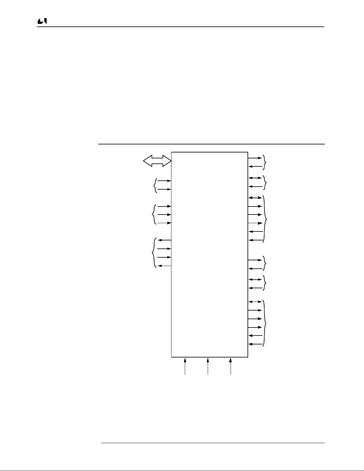
1.4 Pin Functions
The SCC pins are divided into seven functional groups: Address/Data, Bus Timing and
Reset, Device Control, Interrupt, Serial Data (both channels), Peripheral Control (both
channels), and Clocks (both Channels). Figures 1–3 and 1–4 show the pins in each functional group for the 40- and 44-pin SCC versions.
The Address/Data group consists of the bidirectional lines used to transfer data between
the CPU and the SCC. The direction of these lines depends on whether the SCC is selected and whether the operation is a Read or a Write.
The Timing and Control groups designate the type of transaction to occur and when this
transaction will occur. The Interrupt group provides inputs and outputs to conform to the
Z-Bus specifications for handling and prioritizing interrupts. The remaining groups are divided into Channel A and Channel B groups for serial data (transmit or receive), peripheral control (such as DMA or Modem), and the input and output lines for the receive and
transmit clocks.
Data
Bus
Bus
Timing
and Reset
Control
Interrupt
8
D0- D
7
RD
WR
A/B
CE
D/C
INT
INTACK
IEI
IEO
Am85C30/
Am8530H
SCC
TxDA
RxDA
TRxCA
RTxCA
SYNCA
W/REQA
DTR/REQA
RTSA
CTSA
DCDA
TxDB
RxDB
TRxCB
RTxCB
SYNCB
W/REQB
DTR/REQB
RTSB
CTSB
DCDB
Serial
Data
Channel
Clocks
Channel
Controls
for Modem,
DMA, or
Other
Serial
Data
Channel
Clocks
Channel
Controls
for Modem,
DMA, or
Other
1–6
+5 V PCLK
GND
Figure 1–3. SCC Pin Functions
10216A-004A

General Information AMD
D
D
D
D
INT
IEO
IEI
INTACK
+5 V
W/REQA
SYNCA
RTxCA
RxDA
TRxCA
TxDA
DTR/REQA
RTSA
CTSA
DCDA
PCLK
7
INT
D
1
1
2
3
3
5
4
7
5
6
7
Am8530H
8
Am85C30
9
10
11
12
14
15
16
17
18
19
20
5
3
D
D
0
1
D
D
D
40
39
38
37
36
35
34
33
32
31
W/REQB
30
29
SYNCB
2813
RTxCB
27
RxDB
26
TRxCB
25
TxDB
DTR/REQB
24
RTSB
23
CTSB
22
DCDB
21
2D4D6
D
0
D
2
D
4
D
6
RD
WR
A/B
CE
D/C
GND
RD
WR
IEO
IEI
INTACK
+5 V
W/REQA
SYNCA
RTxCA
RxDA
TRxCA
TxDA
NC
7
8
9
10
11
12
13
14
15
16
17
6 5
NC
/REQA
DTR
4 3 2 1
Am85C30
RTSA
CTSA
DCDA
PCLK
DCDB
CTSB
RTSB
4041424344
2827262524232221201918
DTR/REQB
39
38
37
36
35
34
33
32
31
30
29
NC
A/B
CE
D/C
NC
GND
W/REQB
SYNCB
RTxCB
RxDB
TRxCB
TxDB
Figure 1–4. Pin Designation for 40- and 44-Pin SCC
10216A-003A
1–7

General InformationAMD
1.5 PIN DESCRIPTIONS
Figure 1–4 designates the pin locations and signal names for the 40- and 44-pin SCC
versions.
1.5.1 System Interface Pin Descriptions
A/B — Channel A/Channel B Select (input, Channel A active High)
This signal selects the channel in which the Read or Write operation occurs and must be
valid prior to the read or write strobe.
CE — Chip Enable (input, active Low)
This signal selects the SCC for operation. It must remain active throughout the bus
transaction.
D0–D7 — Data Lines (bidirectional, 3-state)
These I/O lines carry data or control information to and from the SCC.
D/C — Data/Control (input, data active High)
This signal defines the type of information transfer performed by the SCC: data or control.
The state of this signal must be valid prior to the read or write strobe.
RD — Read (input, active Low)
This signal indicates a Read operation and, when the SCC is selected, enables the SCC
bus drivers. During the interrupt acknowledge cycle, this signal gates the interrupt vector
onto the bus provided that the SCC is the highest priority device requesting an interrupt.
WR — Write (input, active Low)
When the SCC is selected, this signal indicates a Write operation. On the NMOS
Am8530H data must be valid prior to the rising edge of write strobe. The Am85C30 does
not share this requirement. The coincidence of RD and WR is interpreted as a Reset.
IEI* — Interrupt Enable In (input, active High)
IEI is used with IEO to form an interrupt daisy chain when there is more than one interrupt-driven device. A High on IEI indicates that no other higher priority device has an Interrupt Under Service (IUS) or is requesting an interrupt.
IEO — Interrupt Enable Out (output, active High)
IEO is High only if IEI is High and the CPU is not servicing an SCC or SCC interrupt or
the controller is not requesting an interrupt (interrupt acknowledge cycle only). IEO is connected to the next lower priority device’s IEI input and thus inhibits interrupts from lower
priority devices.
INTACK* — Interrupt Acknowledge (input, active Low)
This signal indicates an active interrupt acknowledge cycle. During this cycle, the interrupt
daisy chain settles. When RD becomes active, the SCC places an interrupt vector on the
data bus (if IEI is High). INTACK is latched by the rising edge of PCLK.
INT — Interrupt Request (output, open-drain, active Low)
This signal is activated when the SCC is requesting an interrupt.
Note:
1–8
*Pull-up resistors are needed on INTACK and IEI inputs if they are not driven by the
system and for the INT output. If INTACK or IEI are left floating, the Am85C30 will
malfunction. INT is an open drain output and must be pulled up to keep a logical high
level.

General Information AMD
1.5.2 Serial Channel Pin Descriptions
CTSA, CTSB — Clear to Send (inputs, active Low)
If the Auto Enable bit in WR3 (D5) is set, a Low on these inputs enables the respective
transmitter; otherwise they may be used as general-purpose inputs. Both inputs are
Schmitt-trigger buffered to accommodate slow rise-time inputs. The SCC detects transitions on these inputs and, depending on whether or not other External/Status Interrupts
are pending, can interrupt the processor on either logic level transitions.
DCDA, DCDB — Data Carrier Detect (inputs, active Low)
These pins function as receiver enables if the Auto Enable bit in WR3 (D5) is set; otherwise they may be used as general-purpose input pins. Both pins are Schmitt-trigger buffered to accommodate slow rise-time signals. The SCC detects transitions on these inputs
and, depending on whether or not other External/Status Interrupts are pending, can interrupt the processor on either logic level transitions.
DTR/REQA, DTR/REQB — Data Terminal Ready/Request (outputs, active Low)
These pins function as DMA requests for the transmitter if bit D2 of WR14 is set; otherwise they may be used as general-purpose outputs following the state programmed into
the DTR bit.
PCLK — Clock (input)
This is the master clock used to synchronize internal signals. PCLK is not required to
have any phase relationship with the master system clock.
RTSA, RTSB — Request to Send (outputs, active Low)
When the Request to Send (RTS) bit in WR5 is set, the RTS pin goes Low. When the
RTS bit is reset in the Asynchronous mode and the Auto Enable bit in WR3 (D5) is set,
the signal goes High after the transmitter is empty. In Synchronous mode or Asynchronous mode with the Auto Enable bit reset, the RTS pins strictly follow the state of the RTS
bits. Both pins can be used as general-purpose outputs. Request to send outputs are not
affected by the state of the Auto Enable (D5) bit in WR3 in synchronous mode.
RTxCA, RTxCB — Receive/Transmit Clocks (inputs, active Low)
The functions of these pins are under program control. In each channel, RTxC may supply the receive clock, the transmit clock, the clock for the baud rate generator, or the clock
for the digital phase-locked loop. These pins can also be programmed for use with the
respective SYNC pins as a crystal oscillator. The receive clock may be 1, 16, 32, or 64
times the data rate in Asynchronous mode.
If a clock is supplied on these pins in NRZI or NRZ mode serial data on the RxD pin will
be sampled on the rising edge of these pins. In FM mode, RxD is sampled on both clock
edges.
RxDA, RxDB — Receive Data (inputs, active High)
Serial data is received through these pins.
SYNCA, SYNCB — Synchronization (inputs/outputs, active Low)
These pins can act as either inputs, outputs, or as part of the crystal oscillator circuit. In
the Asynchronous mode (crystal oscillator option not selected), these pins are inputs similar to CTS and DCD. In this mode, transitions on these lines affect the state of the SYNC/
HUNT status bit in Read Register 0, but have no other function.
In External Synchronization mode, with the crystal oscillator not selected, these lines also
act as inputs. In this mode, SYNC must be driven Low two receive clock cycles after the
last bit of the sync character is received. Character assembly begins on the rising edge of
the receive clock immediately following the activation of SYNC.
In the Internal Synchronization mode (Monosync and Bisync), with the crystal oscillator
not selected, these pins act as outputs and are active only during the part of the receive
clock cycle in which sync characters are recognized. The sync condition is not latched, so
1–9

General InformationAMD
these outputs are active each time a sync character is recognized (regardless of character boundaries). In SDLC mode, these pins act as outputs and are valid on receipt of a
flag.
TRxCA, TRxCB — Transmit/Receive Clocks (inputs or outputs, active Low)
The functions of these pins are under program control. TRxC may supply the receive
clock or the transmit clock in the Input mode or supply the output of the digital phaselocked loop, the crystal oscillator, the baud rate generator, or the transmit clock in the output mode. If a clock is supplied on these pins in NRZI or NRZ mode serial data on the
TxD pin will be clocked out on the negative edge of these pins. In FM mode, TxD is
clocked on both clock edges.
TxDA, TxDB — Transmit Data (outputs, active High)
Serial data from the SCC is sent out these pins.
W/REQA, W/REQB — Wait/Request (outputs, open drain and switches from floating
to Low when programmed for Wait function, driven from High to Low when programmed for a Request function)
These dual-purpose outputs can be programmed as either transmit or receive request
lines for a DMA controller, or as Wait lines to synchronize the CPU to the SCC data rate.
The reset state is Wait.
1–10

CHAPTER 2
System Interface
2.1 Introduction 2–3. . . . . . . . . . . . . . . . . . . . . . . . . . . . . . . . . . . . . . . . . . . . . . . . . . .
2.2 Registers 2–3. . . . . . . . . . . . . . . . . . . . . . . . . . . . . . . . . . . . . . . . . . . . . . . . . . . . .
2.3 System Timings 2–5. . . . . . . . . . . . . . . . . . . . . . . . . . . . . . . . . . . . . . . . . . . . . . . .
2.3.1 Read Cycle 2–5. . . . . . . . . . . . . . . . . . . . . . . . . . . . . . . . . . . . . . . . . . . . .
2.3.2 Write Cycle 2–5. . . . . . . . . . . . . . . . . . . . . . . . . . . . . . . . . . . . . . . . . . . . .
2.3.3 Interrupt Acknowledge Cycle 2–5. . . . . . . . . . . . . . . . . . . . . . . . . . . . . . . .
2.4 Register Access 2–6. . . . . . . . . . . . . . . . . . . . . . . . . . . . . . . . . . . . . . . . . . . . . . .
2.5 Am85C30 Enhancement Register Access 2–7. . . . . . . . . . . . . . . . . . . . . . . . . . .
2.6 Reset 2–12. . . . . . . . . . . . . . . . . . . . . . . . . . . . . . . . . . . . . . . . . . . . . . . . . . . . . . . .
2–1

AMD
System Interface
2–2

CHAPTER 2
System Interface
2.1 INTRODUCTION
The SCC internal structure provides all the interrupt and control logic necessary to interface with non-multiplexed buses. Interface logic is also provided to monitor modem or
peripheral control inputs or outputs. All of the control signals are general-purpose and can
be applied to various peripheral devices as well as used for modem control.
The center for data activity revolves around the internal read and write registers. The programming of these registers provides the SCC with functional “personality;” i.e. register
values can be assigned before or during program sequencing to determine how the SCC
will establish a given communication protocol.
This chapter covers the details of interfacing the SCC to a system. The general timing
requirements are described but the respective data sheets must be referred to for specific
A.C. numbers.
2.2 REGISTERS
All modes of communication are established by the bit values of the write registers. As
data are received or transmitted, read register values may change. These changed values can promote software action or internal hardware action for further register changes.
The register set for each channel includes several write and read registers. Ten write registers are used for control, two for sync character generation, and two for the on-chip
baud rate generator. Two additional write registers are shared by both channels; one is
used as the interrupt vector and one as the master interrupt control. Both registers are
accessed and shared by either channel.
Six read registers indicate status functions; two are used by the baud rate generator, and
one by the receiver buffer. The remaining two read registers are shared by both channels;
one for interrupt pending bits and one for the interrupt vector. On the Am85C30 three additional registers are available. Refer to Chapter 4 and Chapter 6 for further details on
these registers.
Table 2–1 summarizes the assigned functions for each read and write register. Chapter 6
provides a detailed bit legend and description of each register.
2–3

System InterfaceAMD
Table 2–1. Register Set
Read Register Functions
RR0 Transmit/Receive buffer status, and External status
RR1 Special Receive Condition status, residue codes, error conditions
RR2 Modified (Channel B only) interrupt vector and Unmodified interrupt
vector (Channel A only)
RR3 Interrupt Pending bits (Channel A only)
*RR6 14-bit frame byte count (LSB)
*RR7 14-bit frame byte count (MSB), frame status
RR8 Receive buffer
RR10 Miscellaneous XMTR, RCVR status parameters
RR12 Lower byte of baud rate generator time constant
RR13 Upper byte of baud rate generator time constant
RR15 External/Status interrupt control information
* Available only when Am85C30 is programmed in enhanced mode.
Write Register Functions
WR0 Command Register, (Register Pointers), CRC initialization, resets
for various modes
WR1 Interrupt conditions, Wait/DMA request control
WR2 Interrupt vector (access through either channel)
WR3 Receive/Control parameters, number of bits per character, Rx CRC
enable
WR4 Transmit/Receive miscellaneous parameters and codes, clock rate,
number of sync characters, stop bits, parity
WR5 Transmit parameters and control, number of Tx bits per character,
Tx CRC enable
WR6 Sync character (1st byte) or SDLC address
WR7 SYNC character (2nd byte) or SDLC flag
**WR7′ SDLC options; auto flag, RTS, EOM reset, extended read, etc.
WR8 Transmit buffer
WR9 Master interrupt control and reset (accessed through either
channel), reset bits, control interrupt daisy chain
WR10 Miscellaneous transmitter/receiver control bits, NRZI, NRZ, FM
encoding, CRC reset
WR11 Clock mode control, source of Rx and Tx clocks
WR12 Lower byte of baud rate generator time constant
WR13 Upper byte of baud rate generator time constant
WR14 Miscellaneous control bits: baud rate generator, Phase-Locked
Loop control, auto echo, local loopback
WR15 External/Status interrupt control information-control external
conditions causing interrupts
** Only available in Am85C30.
2–4

System Interface AMD
2.3 SYSTEM TIMINGS
Two control signals, RD and WR, are used by the SCC to time bus transactions. In addition, four other control signals, CE, D/C, A/B and INTACK are used to control the type of
bus transaction that will occur.
A bus transaction starts when the D/C and A/B pins are asserted prior to the negative
edge of the RD or WR signal. The coincidence of CE and RD or CE and WR latches the
state of D/C and A/B and starts the internal operation. The INTACK signal must have
been previously sampled High by a rising edge of PCLK for a read or write cycle to occur.
In addition to sampling INTACK, PCLK is used by the interrupt section to set the Interrupt
Pending (IP) bits.
The SCC generates internal control signals in response to a register access. Since RD
and WR have no phase relationship with PCLK, the circuitry generating these internal
control signals provide time for metastable conditions to disappear. This results in a recovery time related to PCLK. This recovery time applies only between transactions involving the Am8530H/Am85C30, and any intervening transactions are ignored. This recovery
time is four PCLK cycles, measured from the falling edge of RD or WR for a read or write
cycle of any SCC register on the Am8530H-step and 3 or 3.5 PCLK cycles for the
Am85C30.
Note that RD and the WR inputs are ignored until CE is activated. The falling edge of RD
and WR can be substituted for the falling edge of CE or vice versa for calculating proper
pulse width for RD or WR low. In other words, if CE goes active after RD or WR have
gone active for a read or a write cycle, respectively, CE must stay active as long as the
minimum pulse width for RD and WR.
2.3.1 Read Cycle
The Read cycle timing for the SCC is shown in Figure 2–1. The A/B and D/C pins are
latched by the coincidence of RD and CE active. CE must remain Low and INTACK must
remain High throughout the cycle. The SCC bus drivers are enabled while CE and RD are
both Low. A read with D/C High does not disturb the state of the pointers and a read cycle
with D/C Low resets the pointers to zero after the internal operation is complete.
2.3.2 Write Cycle
The Write cycle timing for the SCC is shown in Figure 2–2. The A/B and D/C pins are
latched by the coincidence of WR and CE active. CE must remain Low and INTACK must
remain High throughout the cycle. A write cycle with D/C High does not disturb the state
of the pointers and a write cycle with D/C Low resets the pointers to zero after the internal
operation is complete.
2.3.3 Interrupt Acknowledge Cycle
The Interrupt Acknowledge cycle timing for the SCC is shown in Figure 2–3. The state of
INTACK is latched by the rising edge of PCLK. While INTACK is Low, the state of the
A/B, D/C, and WR pins is ignored by the SCC. Between the time INTACK is first sampled
Low and the time RD falls, the internal and external IEI/IEO daisy chains settle; this is
A.C. parameter #38 TdlAi (RD).
If there is an interrupt pending in the SCC, and IEI is High when RD falls, the Interrupt
Acknowledge cycle is intended for the SCC. This being the case, the SCC sets the appropriate Interrupt Under Service (IUS) latch, and places an interrupt vector on D0–D7. If the
falling edge of RD sets an IUS bit in the SCC, the INT pin goes inactive in response to the
falling edge. Note that there should be only one RD per Acknowledge cycle.
Another important fact is that the IP bits in the SCC are updated by a clock half the frequency of PCLK, and this clock is stopped while the pointers point to RR2 and RR3; thus
the interrupt requests will be delayed if the pointers are left pointing at these registers.
2–5

System InterfaceAMD
2.4 REGISTER ACCESS
The registers in the SCC are accessed in a two-step process, using a Register Pointer to
perform the addressing. To access a particular register, the pointer bits must be set by
writing to WR0. The pointer bits may be written in either channel because only one set
exists in the SCC. After the pointer bits are set, the next read or write cycle of the SCC
having D/C Low will access the desired register. At the conclusion of this read or write
cycle, the pointer bits are automatically reset to ‘0’, so that the next control write will be to
the pointers in WR0.
A read from RR8 (the Receive Buffer) or a write to WR8 (Transmit Buffer) may either be
done in this fashion or by accessing the SCC having the D/C pin High. A read or write
with D/C High accesses the receive or transmit buffers directly, and independently, of the
state of the pointer bits. This allows single-cycle access to the receive or transmit buffers
and does not disturb the pointer bits. The fact that the pointer bits are reset to ‘0’, unless
explicitly set otherwise, means that WR0 and RR0 may also be accessed in a single cycle. That is, it is not necessary to write the pointer bits with ‘0’ before accessing WR0 or
RR0. There are three pointer bits in WR0, and these allow access to the registers with
addresses 0 through 7. Note that a command may be written to WR0 at the same time
that the pointer bits are written. To access the registers with addresses 8 through 15, a
special command (point high in WR0) must accompany the pointer bits. This precludes
concurrently issuing a command (point high in WR0) when pointing to these registers.
The SCC register map is shown in Table 2–2. PNT
D0 in WR0, respectively.
If for some reason the state of the pointer bits is unknown, they may be reset to ‘0’ by performing a read cycle with the D/C pin held Low. Once the pointer bits have been set, the
desired channel is selected by the state of the A/B pin during the actual read or write of
the desired register.
, PNT1 and PNT0 are bits D2, D1 and
2
A/B, D/C
INTACK
RD
D0- D
CE
Address Valid
7
Data Valid
10216A-009A
Figure 2–1. SCC Read Cycle
2–6

System Interface AMD
D
0
PCLK
– D
A/B, D/C
INTACK
WR
D0- D
7
CE
Address Valid
7
Data Valid
10216A-010A
Figure 2–2. SCC Write Cycle
Vector
RD
INTACK
IEI
IEO
INT
Figure 2–3. Interrupt Acknowledge Cycle
2.5 Am85C30 Enhancement Register Access
SDLC/HDLC enhancements on the Am85C30 are enabled or disabled via bits D2 and D0
in WR15. Bit D2 determines whether or not the 10x19-bit SDLC/HDLC frame status FIFO
is enabled while bit D0 determines whether or not other SDLC/HDLC mode enhancements are enabled via WR7’. Table 2–3 shows what functions on the Am85C30 are enabled when these bits are set.
When bit D2 of WR15 is set to ‘1’, two additional registers (RR6 and RR7) per channel
specific to the 10x19-bit frame status FIFO are made available. The Am85C30 register
map when this function is enabled is shown in Table 2–4.
2–7

Table 2–2. SCC Register Map
System InterfaceAMD
A/B PNT
2
PNT
1
PNT
WRITE READ
0
0 0 0 0 WR0B RR0B
0 0 0 1 WR1B RR1B
0 0 1 0 WR2 RR2B
0 0 1 1 WR3B RR3B
0 1 0 0 WR4B (RR0B)
0 1 0 1 WR5B (RR1B)
0 1 1 0 WR6B (RR2B)
0 1 1 1 WR7B (RR3B)
1 0 0 0 WR0A RR0A
1 0 0 1 WR1A RR1A
1 0 1 0 WR2 RR2A
1 0 1 1 WR3A RR3A
1 1 0 0 WR4A (RR0A)
1 1 0 1 WR5A (RR1A)
1 1 1 0 WR6A (RR2A)
1 1 1 1 WR7A (RR3A)
Table 2–2. SCC Register Map (Continued)
A/B PNT
2
PNT
1
PNT
WRITE READ
0
With the Point High command: [D5–3 (WR0) = 001]
0 0 0 0 WR8B RR8B
0 0 0 1 WR9 (RR13B)
0 0 1 0 WR10B RR10B
0 0 1 1 WR11B (RR15B)
0 1 0 0 WR12B RR12B
0 1 0 1 WR13B RR13B
0 1 1 0 WR14B (RR10B)
0 1 1 1 WR15B RR15B
1 0 0 0 WR8A RR8A
1 0 0 1 WR9 (RR13A)
1 0 1 0 WR10A RR10A
1 0 1 1 WR11A (RR15A)
1 1 0 0 WR12A RR12A
1 1 0 1 WR13A RR13A
1 1 1 0 WR14A (RR10A)
1 1 1 1 WR15A RR15A
2–8

System Interface AMD
Table 2–3. Enhancement Options
WR15 bit D2 WR15 D0 WR7′ bit D6
10x19-bit SDLC/HDLC Extended
FIFO Enabled Enhance Enabled Read Enable Functions Enabled
1 0 x 10x19-bit FIFO enhancement
enabled only
0 1 0 SDLC/HDLC enhancements
enabled only
0 1 1 SDLC/HDLC enhancements
enabled with extended read
enabled
1 1 0 10x19-bit FIFO and SDLC/
HDLC enhancements enabled
1 1 1 10x19-bit FIFO and SDLC/
HDLC enhancements with
extended read enabled
Bit D0 of WR15 determines whether or not other enhancements pertinent only to SDLC/
HDLC Mode operation are available for programming via WR7′ as shown below. Write
Register 7 prime (WR7′ ) can be written to when bit D0 of WR15 is set to ‘1’. When this
bit is set, writing to WR7 (flag register) actually writes to WR7′. If bit D6 of this register is
set to ‘1’, previously unreadable registers WR3, WR4, WR5, WR10 are readable by the
processor. In addition, WR7′ is also readable by having this bit set. WR3 is read when a
bogus RR9 register is accessed during a read cycle, WR10 is read by accessing RR11,
and WR7′ is accessed by executing a read to RR14. The Am85C30 register map with bit
D0 of WR15 and bit D6 of WR7′ set is shown in Table 2–5.
2–9

Table 2–4. 10 x 19-Bit FIFO Enabled
System InterfaceAMD
A/B PNT
2
PNT
1
PNT
WRITE READ
0
0 0 0 0 WR0B RR0B
0 0 0 1 WR1B RR1B
0 0 1 0 WR2 RR2B
0 0 1 1 WR3B RR3B
0 1 0 0 WR4B (RR0B)
0 1 0 1 WR5B (RR1B)
0 1 1 0 WR6B RR6B
0 1 1 1 WR7B RR7B
1 0 0 0 WR0A RR0A
1 0 0 1 WR1A RR1A
1 0 1 0 WR2 RR2A
1 0 1 1 WR3A RR3A
1 1 0 0 WR4A (RR0A)
1 1 0 1 WR5A (RR1A)
1 1 1 0 WR6A RR6A
1 1 1 1 WR7A RR7A
With the Point High command:
0 0 0 0 WR8B RR8B
0 0 0 1 WR9 (RR13B)
0 0 1 0 WR10B RR10B
0 0 1 1 WR11B (RR15B)
0 1 0 0 WR12B RR12B
0 1 0 1 WR13B RR13B
0 1 1 0 WR14B (RR10B)
0 1 1 1 WR15B RR15B
1 0 0 0 WR8A RR8A
1 0 0 1 WR9 (RR13A)
1 0 1 0 WR10A RR10A
1 0 1 1 WR11A (RR15A)
1 1 0 0 WR12A RR12A
1 1 0 1 WR13A RR13A
1 1 1 0 WR14A (RR10A)
1 1 1 1 WR15A RR15A
2–10

System Interface AMD
Table 2–5. SDLC/HDLC Enhancements Enabled
A/B PNT
2
PNT
1
PNT
WRITE READ
0
0 0 0 0 WR0B RR0B
0 0 0 1 WR1B RR1B
0 0 1 0 WR2 RR2B
0 0 1 1 WR3B RR3B
0 1 0 0 WR4B RR4B(WR4B)
0 1 0 1 WR5B RR5B(WR5B)
0 1 1 0 WR6B (RR6B)
0 1 1 1 WR7B (RR7B)
1 0 0 0 WR0A RR0A
1 0 0 1 WR1A RR1A
1 0 1 0 WR2 RR2A
1 0 1 1 WR3A RR3A
1 1 0 0 WR4A RR4A(WR4A)
1 1 0 1 WR5B RR5A(WR5A)
1 1 1 0 WR6A (RR2A)
1 1 1 1 WR7A (RR3A)
With the Point High command:
0 0 0 0 WR8B RR8B
0 0 0 1 WR9 RR9(WR3B)
0 0 1 0 WR10B RR10B
0 0 1 1 WR11B RR11B(WR10B)
0 1 0 0 WR12B RR12B
0 1 0 1 WR13B RR13B
0 1 1 0 WR14B RR14B(WR7’B)
0 1 1 1 WR15B RR15B
1 0 0 0 WR8A RR8A
1 0 0 1 WR9 RR9A(WR3A)
1 0 1 0 WR10A RR10A
1 0 1 1 WR11A RR11A(WR10A)
1 1 0 0 WR12A RR12A
1 1 0 1 WR13A RR13A
1 1 1 0 WR14A RR14A(WR7’A)
1 1 1 1 WR15A RR15A
D0D1D2D3D4D5D6D7
0
Ext.
Read
Enable
Rx
comp.
CRC
DTR/REQ
Fast
Mode
Force
Txd
High
Auto
RTS
Turnoff
Auto
EOM
Reset
Auto
Tx
Flag
WR7′—SDLC/HDLC Enhancement
2–11

System InterfaceAMD
If both bits D0 and D2 of WR15 are set to ‘1’ then the Am85C30 register map is as shown
in Table 2–6.
Table 2–6. Register Set—All Enhancements Enabled
A/B PNT
2
PNT
1
PNT
WRITE READ
0
0 0 0 0 WR0B RR0B
0 0 0 1 WR1B RR1B
0 0 1 0 WR2 RR2B
0 0 1 1 WR3B RR3B
0 1 0 0 WR4B RR4B(WR4B)
0 1 0 1 WR5B RR5B(WR5B)
0 1 1 0 WR6B RR6B
0 1 1 1 WR7B RR7B
1 0 0 0 WR0A RR0A
1 0 0 1 WR1A RR1A
1 0 1 0 WR2 RR2A
1 0 1 1 WR3A RR3A
1 1 0 0 WR4A RR4A(WR4A)
1 1 0 1 WR5B RR5A(WR5A)
1 1 1 0 WR6A RR6A
1 1 1 1 WR7A RR7A
With the Point High command:
0 0 0 0 WR8B RR8B
0 0 0 1 WR9 RR9B(WR3B)
0 0 1 0 WR10B RR10B
0 0 1 1 WR11B RR11B(WR10B)
0 1 0 0 WR12B RR12B
0 1 0 1 WR13B RR13B
0 1 1 0 WR14B RR14B(WR7’B)
0 1 1 1 WR15B RR15B
1 0 0 0 WR8A RR8A
1 0 0 1 WR9 RR9A(WR3A)
1 0 1 0 WR10A RR10A
1 0 1 1 WR11A RR11A(WR10A)
1 1 0 0 WR12A RR12A
1 1 0 1 WR13A RR13A
1 1 1 0 WR14A RR14A(WR7’A)
1 1 1 1 WR15A RR15A
2.6 RESET
The SCC may be reset by either hardware or software. A hardware reset occurs when
RD and WR are both Low, simultaneously regardless of the state of the CE input, which
is normally an illegal condition. As long as both RD and WR are Low, the SCC recognizes
the reset condition. Once this condition is removed, however, the reset condition is asserted internally for an additional four to five PCLK cycles. During this time, any attempt
to access the SCC will be ignored. However a hardware reset does not clear the receive
FIFO, therefore it may be necessary to perform a few dummy reads immediately after a
2–12

System Interface AMD
hardware reset to ensure that the FIFO is completely flushed before the new data can be
received reliably.
The SCC has three software resets encoded into command bits in WR9. There are two
channel resets, which affect only one channel in the device and some of the bits in the
write registers. The third command forces the same result as a hardware reset. As in the
case of a hardware reset, the SCC stretches the reset signal an additional four to five
PCLK cycles beyond the ordinary valid access recovery time. When the SCC is first powered up, performing a read with the D/C pin held Low will guarantee that the pointers are
reset to ‘0’; then a reset command can be issued by selecting WR9 and writing to it. The
bits in WR9 may be written at the same time as the reset command because these bits
are affected only by a hardware reset. The reset values of the various registers are
shown in Figure 2–4.
Hardware Reset Channel Reset
76543210
00 00 00 00
00 . 0 0. 00 00. 0 0. 00
.. .. .. ..
.. .. .. .
.. .. . ..
0. . 000 0. 0. . 0 00 0.
.......
.
.. .. .. .. .. .. .. ..
11 00 00 . . .. 0
00 00 00 00 0. . 0 00 00
00 00 10 00
.. .. .. .. .. .. .. ..
0 0
1 1
76543210
00 00 00 00
.. .. .. ..
.. .. .. .
.. .. . ..
.. .. .. ..
.....
.. .. .. ..
WR0
WR1
WR2
WR3
WR4
WR5
WR6
WR7
WR9
WR10
WR11
WR12
.. .. .. .. .. .. .. ..
. . 1000 00 . . 1000 . .
11 11 10 00 11 11 10 00
01.. .100 01...100
00 00 01 10 00 00 01 10
00 00 00 00 00 00 00 00
00 00 00 00 00 00 00 00
Figure 2–4. SCC Register Reset Values
WR13
WR14
WR15
RR0
RR1
RR3
RR10
2–13

CHAPTER 3
I/O Programming Functional
Description
3.1 Introduction 3–3. . . . . . . . . . . . . . . . . . . . . . . . . . . . . . . . . . . . . . . . . . . . . . . . . .
3.2 Polling 3–3. . . . . . . . . . . . . . . . . . . . . . . . . . . . . . . . . . . . . . . . . . . . . . . . . . . . . . .
3.3 Interrupt Sources 3–3. . . . . . . . . . . . . . . . . . . . . . . . . . . . . . . . . . . . . . . . . . . . . . .
3.4 Interrupt Control 3–4. . . . . . . . . . . . . . . . . . . . . . . . . . . . . . . . . . . . . . . . . . . . . . .
3.4.1 Interrupt Enable Bit 3–4. . . . . . . . . . . . . . . . . . . . . . . . . . . . . . . . . . . . . . .
3.4.2 Interrupt Pending Bit 3–5. . . . . . . . . . . . . . . . . . . . . . . . . . . . . . . . . . . . . .
3.4.3 Interrupt Under Service Bit 3–5. . . . . . . . . . . . . . . . . . . . . . . . . . . . . . . . .
3.4.4 Disable Lower Chain Bit 3–5. . . . . . . . . . . . . . . . . . . . . . . . . . . . . . . . . . .
3.5 Interrupt Operations 3–6. . . . . . . . . . . . . . . . . . . . . . . . . . . . . . . . . . . . . . . . . . . .
3.5.1 Multiple Interrupt Priority Resolution 3–6. . . . . . . . . . . . . . . . . . . . . . . . . .
3.5.2 Interrupt Without Acknowledge 3–8. . . . . . . . . . . . . . . . . . . . . . . . . . . . . .
3.5.3 Interrupt With Acknowledge With Vector 3–8. . . . . . . . . . . . . . . . . . . . . . .
3.5.4 Interrupt With Acknowledge Without Vector 3–10. . . . . . . . . . . . . . . . . . . .
3.5.5 Lower Priority Interrupt Masking 3–10. . . . . . . . . . . . . . . . . . . . . . . . . . . . .
3.6 Receive Interrupts 3–10. . . . . . . . . . . . . . . . . . . . . . . . . . . . . . . . . . . . . . . . . . . . . .
3.6.1 Receive Interrupts Disabled 3–10. . . . . . . . . . . . . . . . . . . . . . . . . . . . . . . .
3.6.2 Receive Interrupt on First Character or
Special Condition 3–10. . . . . . . . . . . . . . . . . . . . . . . . . . . . . . . . . . . . . . . . .
3.6.3 Receive Interrupt on All Receive Characters or
Special Conditions 3–11. . . . . . . . . . . . . . . . . . . . . . . . . . . . . . . . . . . . . . . .
3.6.4 Receive Interrupt on Special Conditions 3–11. . . . . . . . . . . . . . . . . . . . . . .
3.7 Transmit Interrupts 3–12. . . . . . . . . . . . . . . . . . . . . . . . . . . . . . . . . . . . . . . . . . . . .
3.8 External/Status Interrupts 3–13. . . . . . . . . . . . . . . . . . . . . . . . . . . . . . . . . . . . . . . .
3.8.1 Sync/Hunt 3–13. . . . . . . . . . . . . . . . . . . . . . . . . . . . . . . . . . . . . . . . . . . . . .
3.8.2 Break/Abort 3–14. . . . . . . . . . . . . . . . . . . . . . . . . . . . . . . . . . . . . . . . . . . . .
3.8.3 Zero Count 3–14. . . . . . . . . . . . . . . . . . . . . . . . . . . . . . . . . . . . . . . . . . . . . .
3.8.4 Tx Underrun/EOM 3–15. . . . . . . . . . . . . . . . . . . . . . . . . . . . . . . . . . . . . . . .
3.8.5 Clear To Send 3–15. . . . . . . . . . . . . . . . . . . . . . . . . . . . . . . . . . . . . . . . . . .
3.8.6 Data Carrier Detect 3–15. . . . . . . . . . . . . . . . . . . . . . . . . . . . . . . . . . . . . . .
3.9 Block Transfers 3–15. . . . . . . . . . . . . . . . . . . . . . . . . . . . . . . . . . . . . . . . . . . . . . . .
3.9.1 Wait on Transmit 3–16. . . . . . . . . . . . . . . . . . . . . . . . . . . . . . . . . . . . . . . . .
3.9.2 Wait on Receive 3–16. . . . . . . . . . . . . . . . . . . . . . . . . . . . . . . . . . . . . . . . .
3.9.3 DMA Requests 3–17. . . . . . . . . . . . . . . . . . . . . . . . . . . . . . . . . . . . . . . . . .
3.9.3.1 DMA Request on Transmit
(using W/REQ) 3–17. . . . . . . . . . . . . . . . . . . . . . . . . . . . . . . . . . .
3.9.3.2 DMA Request on Transmit
(using DTR/REQ) 3–18. . . . . . . . . . . . . . . . . . . . . . . . . . . . . . . . .
3.9.3.3 DTR/REQ Deactivation Timing 3–19. . . . . . . . . . . . . . . . . . . . . . .
3.9.3.4 DMA Request on Receive (using W/REQ) 3–20. . . . . . . . . . . . . .
3–1

I/O Programming Functional Description
AMD
3–2

CHAPTER 3
I/O Programming Functional
Description
3.1 INTRODUCTION
The SCC can work under one of the following three modes of I/O operations: Polling,
Interrupts, and Block transfer. All three modes involve register manipulation during initialization and data transfer. Regardless of the communication mode selected, all three I/O
operating modes are available for use and must be programmed in the initialization
routine.
3.2 POLLING
Polling avoids interrupts and is the simplest mode to implement. In this mode, the software must poll the SCC to determine when data are to be written or read from the SCC.
This mode is enabled when the Master Interrupt Enable (MIE) bit in WR9 (D3) and the
Wait/DMA Request Enable bit in WR1 (D7) are both set to ‘0’.
In this mode the software must poll RR0 to determine the status of the Receive Buffer,
Transmit Buffer and External/Status before jumping to the appropriate interrupt routine.
3.3 INTERRUPT SOURCES
When the MIE bit in WR9 (D3) is set to ‘1’ interrupts will be enabled and, the SCC as a
microprocessor peripheral, will request an interrupt by asserting the INT pin Low from its
open-drain state only when it needs servicing.
Each channel in the SCC contains three sources of interrupts making a total of six.
These three sources of interrupts are: 1) Receiver, 2) Transmitter, and 3) External/Status
conditions as shown in Figure 3–1. In addition, there are several conditions that may
cause these interrupts. Each interrupt source is enabled under program control, with
Channel A having a higher priority than Channel B and with Receive, Transmit, and External/Status interrupts prioritized respectively within each channel as shown in
Table 3–1.
3–3

INT on 1st Rx Char. or
Special Condition
INT on All Rx Char. or
Special Condition
Rx Int on Special
Condition only
Parity
I/O Programming Functional DescriptionAMD
Receiver
Interrupt
Sources
Transmit Buffer Empty
Zero Count
DCD
SYNC/HUNT
CTS
Tx Underrun/EOM
Break/Abort
Transmitter
Interrupt
Source
External/Status
Interrupt
Sources
Figure 3–1. SCC Interrupts
Table 3–1. Interrupt Source Priority
Receiver Channel A High
Transmit Channel A
External/Status Channel A ↓
Receiver Channel B ↓
Transmit Channel B
External/Status Channel B Low
SCC
Interrupt
3.4 INTERRUPT CONTROL
In addition to the MIE bit that enables or disables all SCC interrupts, three control/status
bits are associated with each interrupt source internal to the SCC. These are the Interrupt
Enable (IE), the Interrupt Pending (IP), and the Interrupt Under Service (IUS) bits. Similarly, lower-priority devices on the external daisy chain can be prevented from requesting
interrupts via the Disable Lower Chain bit in WR9 (D2).
3.4.1 Interrupt Enable Bit
The Interrupt Enable (IE) bits are written by the processor and serve to control interrupt
requests from each interrupt source on the SCC. If the IE bit is set to ‘1’ for an interrupt
source, then that source may cause an interrupt request providing all of the necessary
conditions are met. If the IE bit is reset, no interrupt request will be generated by that
source. The IE bits are write-only and are programmed in WR1 as follows.
3–4

I/O Programming Functional Description AMD
D7
W/DMA
REQ
Enable
D6
W/DMA
REQ
Funct.
D5
W/DMA
REQ on
Rx/Tx
D4 D3 D2
Parity
INT
Enable
— Rx INT Disable
0
0
1
1
0
— Rx INT on 1st Char. or
1
Special Condition
— INT on All Rx Char. or
0
Special Condition
— Rx INT on Special Only
1
D1
Tx
INT
Enable
D0
Ext/Sta
INT
Enable
WR1—Interrupt Source IE
3.4.2 Interrupt Pending Bit
The Interrupt Pending (IP) bit for a given source of interrupt may be set by the presence
of an interrupt condition in the SCC and is reset directly by the processor, or indirectly by
some action that the processor may take. If the corresponding IE bit is not set, the IP for
that source of interrupt will never be set. The IP bits in the SCC are read-only via RR3 as
shown above.
D7
0
D6
0
D5
Ch. A
Rx
IP
D4
Ch. A
Tx
IP
D3
Ch. A
Ext/Sta
IP
D2
Ch. B
Rx
IP
D1
Ch. B
Tx
IP
D0
Ch. B
Ext/Sta
IP
RR3—Interrupt Pending
3.4.3 Interrupt Under Service Bit
The Interrupt Under Service (IUS) bits are not observable by the processor. An IUS bit is
set during an Interrupt Acknowledge cycle for the highest-priority IP. The IUS bit is used
to control the operation of internal and external daisy chain interrupts. The internal daisy
chain links the six sources of interrupt in a fixed order, chaining the IUS bits for each
source. While an internal IUS bit is set, all lower-priority interrupt requests are masked
off; during an Interrupt Acknowledge cycle the IP bits are also gated into the daisy chain.
This insures that the highest-priority IP selected will have its IUS bit set. At the end of an
interrupt service routine, the processor must issue a Reset Highest IUS Command in
WR0 to re-enable lower-priority interrupts. This is the only way, short of a software or
hardware reset, that an IUS bit may be reset.
3.4.4 Disable Lower Chain Bit
The Disable Lower Chain (DLC) bit in WR9 (D2) is used to disable all SCCs in a lower
position on the external daisy chain. If this bit is set to ‘1’, the IEO pin is driven Low and
prevents lower-priority devices from generating an interrupt request. Note that the IUS bit,
when set, will have the same effect but is not controllable through software, and the point
where lower-priority interrupts are masked off may not correspond to the chip boundary.
3–5

I/O Programming Functional DescriptionAMD
3.5 INTERRUPT OPERATIONS
Interrupts from the SCC may be acknowledged with a vector, acknowledged without a
vector, or not acknowledged at all. WR2 is used to hold the interrupt vector returned during an interrupt acknowledge cycle. This vector register can be shared among multiple
interrupt sources; some bits of the vector can be encoded with information that identifies
the interrupt source.
Three bits in WR9 determine whether or not a vector is placed on the bus and whether or
not status is included. The Vector Includes Status (VIS) bit (D0) enables status information to be included in the vector, the Status High/Status Low bit (D4) determines which
bits of the vector are encoded as shown in Figure 3–2, and the No Vector (NV) bit (D1)
enables or disables placing the vector on the bus in response to an interrupt acknowledge
cycle.
V3 V2 V1 Status High/Status Low = 0
V4 V5 V6 Status High/Status Low = 1
0 0 0 Ch B Transmit Buffer Empty
0 0 1 Ch B External/Status Change
0 1 0 Ch B Receive Character Available
0 1 1 Ch B Special Receive Condition
1 0 0 Ch A Transmit Buffer Empty
1 0 1 Ch A External/Status Change
1 1 0 Ch A Receive Character Available
1 1 1 Ch A Special Receive Condition
Figure 3–2. Interrupt Vector Modification
In addition, the SCC can share a common interrupt request line to the processor. An external interrupt priority daisy chain, constructed using IEI and IEO on each SCC, is used
to resolve contention when multiple SCC devices share an interrupt request line. This capability eliminates the need for separate interrupt controllers. An interrupt acknowledge
cycle that includes the generation of an explicit Interrupt Acknowledge signal (INTACK) is
used to select the highest priority SCC asserting INT. Figure 3–3 shows a typical arrangement for four SCCs, labeled A through D, on the daisy chain, where A has the highest
priority and D has the lowest priority.
3.5.1 Multiple Interrupt Priority Resolution
The SCC has an internal priority resolution method to allow the highest priority interrupt to
be serviced first. It uses a daisy chain technique of priority interrupt control whereby other
SCC devices are connected together via an external interrupt daisy chain formed with
their Interrupt Enable Input (IEI) and Interrupt Enable Output (IEO) pins. The six interrupt
sources within each SCC are similarly chained together as shown in Figure 3–4 with
Channel A interrupts being higher-priority than any Channel B interrupts, and with the Receiver, Transmitter, and External/Status interrupts prioritized in that order within each
channel. The overall effect is a daisy chain connecting all internal and external interrupt
sources that allows higher priority interrupt sources to pre-empt lower priority sources
and, in the case of simultaneous interrupt requests, determines which request will be acknowledged.
3–6

I/O Programming Functional Description AMD
5 V
SCC
A
IEI IEO
INT INTACK
SCC
B
IEI IEO
INT INTACK
SCC
C
IEI IEO
INT INTACK
IEI IEO
Figure 3–3. External Daisy Chain
INTERRUPT VECTOR
VIS
IP IE IUS IP IE IUS IP IE IUS
RECEIVER CHANNEL A
INTERRUPT
INTACK INT IEO
IEI
TRANSMIT CHANNEL A
INTERRUPT
IEI INTACK INT IEO
EXTERNAL/STATUS
CHANNEL B INTERRUPT
IEI INTACK
SCC
D
INT INTACK
MIE
DLC
NV
INT
IEO
INTACK
Figure 3–4. Internal Daisy Chain
Each SCC on the daisy chain uses PCLK to latch the state of the Interrupt Acknowledge
signal, INTACK. If a Low INTACK is latched, then the present cycle is an interrupt acknowledge cycle and the daisy chain determines which interrupt source is being acknowledged in the following way. Any interrupt source that has an interrupt pending and is not
masked from the chain will hold its IEO line low. Similarly, sources that are currently under service will also hold their IEO lines low.
All other interrupt sources make IEO follow IEI. The result is that only the highest priority,
unmasked source with an interrupt pending will have a high IEI input. This SCC will be
allowed to transfer its vector to the system bus when the RD strobe is issued during the
interrupt acknowledge cycle.
To ensure that the daisy chain has settled by the time RD gates the vector onto the bus,
the SCC requires a delay between falling edge of INTACK and the falling edge of RD (AC
timing parameter #38, TdlAi(RD)). The internal daisy chain may be controlled by the MIE
bit in WR9. This bit, when reset, has the same effect as pulling the IEI Low, thus disabling
all interrupt requests.
3–7

I/O Programming Functional DescriptionAMD
The interrupt protocol is diagrammed in Figure 3–5. In the quiescent state (i.e. no interrupts pending or under service) each SCC on the daisy chain passes its IEI input through
to its IEO output. An interrupt source that requires servicing requests an interrupt by pulling the INT pin Low if the following conditions exist: 1) interrupt source is enabled (i.e., IE
and MIE bits are set to ‘1’), 2) interrupt source is not already under service (i.e., internal
IUS bit set to ‘0’), 3) no higher priority interrupt is under service (i.e., internal IUS bit set to
‘1’), and 4) an interrupt acknowledge cycle is not currently being executed (i.e., INTACK
is High).
When the processor responds with an Interrupt Acknowledge cycle all SCCs that have
enabled interrupt sources with an interrupt pending or already under service, hold their
IEO outputs lines Low. When RD goes Low, only the highest priority SCC with an interrupt pending will have a high IEI input; this is the interrupt being acknowledged, and that
source’s internal IUS bit will be set to ‘1’.
When servicing of the SCC has completed, the Reset Highest IUS Command in WR0
must be issued to unlock the daisy chain, reset the IUS bit, and enable lower-priority interrupt requests.
3.5.2 Interrupt Without Acknowledge
In this mode, INTACK does not have to be generated, and the INTACK input pin must be
tied High. This allows a simpler hardware design that does not have to meet the Interrupt
Acknowledge timing (AC timing parameter #38,TdlAi(RD)). Soon after the SCC’s INT pin
goes active, an external interrupt controller will jump to the interrupt routine. In the interrupt routine, the code must read RR2 from Channel B to read the vector including status.
When the vector is read from Channel B, it always includes the status regardless of the
VIS bit in WR9 (D0). The status given will decode the highest priority interrupt pending at
the time RR2 is read. Note that the vector is not latched in RR2 so that the next read of
RR2 could produce a different vector if another interrupt occurs; however, accessing RR2
disables it from change during the read operation to prevent an error if a higher interrupt
occurs exactly during the read operation.
Once RR2 is read, the interrupt routine must decode the interrupt pending, and clear the
condition. For example, writing a character to the Transmit Buffer will clear the Transmit
Buffer Empty IP. Removing the interrupt condition clears the IP bit and deactivates
INT, but only if there are no other IP bits set. When the interrupt IP is cleared, RR2
can be read again. This allows the interrupt routine to clear all IPs with one interrupt request to the processor.
3.5.3 Interrupt With Acknowledge With Vector
In this mode of operation, the processor must respond to the activation of INT by activating INTACK. After enough time has elapsed to allow the daisy chain to settle (AC timing
parameter #38,TdlAi(RD)), the SCC sets the IUS bit for the highest priority IP. If the No
Vector bit in WR9 (D1) is reset to ‘0’, the SCC will then place the interrupt vector on the
data bus during the read strobe.
To speed the interrupt response time, the SCC can also modify 3 bits in the vector to indicate status. If it is programmed to include status information in the vector, this status may
be encoded and placed in either bits 1–3 or in bits 4–6 as programmed by the Status
High/Status Low bit in WR9. To include status, the VIS bit in WR9 (D0) must be set to ‘1’.
The service routine must then clear the interrupting condition. For example, writing a
character to the Transmit Buffer will clear the Transmit Buffer empty IP. After the interrupting condition is cleared, the routine can read RR3 to determine if any other IP bits are
set and clear them. At the end of the interrupt routine, a Reset IUS command must then
be issued via WR0 to unlock the daisy chain and enable lower-priority interrupt requests.
This is the only way, short of a software or hardware reset, that an IUS bit may be reset.
3–8

I/O Programming Functional Description AMD
Start
No
No
No
No
Interrupt
Condition
Exits
?
Yes
Specific
Interrupt Enable
(IEx = 1)
?
Yes
Interrupt Pending
Set (IP = 1)
Master
Interrupt Enables
(MIE = 1)
?
Yes
IS
Peripheral
Enable Pin Active
(IEI = H)
?
Yes
Peripheral Requests
Interrupt (INT = L)
CPU Service (IUS = 1)
No
(Option) Check Other
Reset IUS and EXIT
Unit Selected for
Service
Routine
Complete
?
Yes
Internal IP, Bits,
CPU Initiates Status
Decode (INTACK = L)
IEI/IEO Daisy Chain
Settles (Wait for DS)
Has Higher
No
Priority Peripheral
Disabled Unit?
Yes
CPU Services Higher
Priority Peripheral
Complete
Yes
Interrupt
Still Pending
(IEI = L)
Priority
Service
?
(IP = 1)
?
No
Yes
No
Figure 3–5. Interrupt Protocol
3–9

I/O Programming Functional DescriptionAMD
3.5.4 Interrupt With Acknowledge Without Vector
If the No Vector bit in WR9 (D1) is set to ‘1’, the SCC will not place the vector on the data
bus during the Interrupt Acknowledge cycle. An external interrupt controller must then
vector the code to the interrupt routine. The interrupt routine must then read RR2 from
Channel B to read the status. This is the same as the case of an interrupt without an acknowledge except that INTACK needs to be generated. The IUS is set as before, and the
vector read in RR2 will not change until the Reset IUS command in WR0 is issued.
3.5.5 Lower Priority Interrupt Masking
The NMOS SCC’s ability to mask lower priority interrupts is done via the IUS bit. This bit
is internal to the SCC and is not observable by the processor. Being able to automatically
mask lower priority interrupts allows a modular approach to coding interrupt routines.
However, using the masking capabilities of the NMOS SCC requires that the INTACK cycle be generated. In applications where an external interrupt controller is being used to
supply the vector, having to generate INTACK through external hardware, in order to use
this capability, is an unnecessary expense.
On the CMOS SCC if bit D5 in WR9 is set to ‘1’, the INTACK cycle does not need to be
generated in order to have the IUS bit set and must be tied High. When this bit is set and
an interrupt occurs, reading RR2 will cause the IUS bit to be set for the highest priority IP.
After the interrupting condition is cleared, the routine can then read RR3 to determine if
any other IPs are set and clear them. At the end of the interrupt routine, a Reset IUS
command must be issued to unlock the internal daisy chain, and reset the IUS bit. Note
that in this mode the No Vector and Vector Includes Status bits in WR9 are ignored.
3.6 RECEIVE INTERRUPTS
Four receive interrupt modes are available on the SCC. These four modes are: 1) Receive Interrupts Disabled, 2) Interrupt on First Character or Special Condition, 3) Interrupt
on All Received Characters or Special Condition, and 4) Receive Interrupt on Special
Condition Only.
The mode selected is controlled by bits D4 and D3 of WR1. The Special Condition interrupts are: Receive FIFO Overrun, CRC/Framing Error, EOF, and Parity. The Parity condition can either be included as a Special Condition or not depending on bit D2 in WR1.
The Special Condition status can be read via RR1.
3.6.1 Receive Interrupts Disabled
This mode prevents the receiver from requesting an interrupt. It is used in a polled environment where either RR0 or the modified vector in RR2 (Channel B) is read for status.
When either RR0 or RR2 indicates that a received character has reached the top of the
Receive Data FIFO, the status should be read first and then RR8 because reading RR8
moves the next character in the Receive Data FIFO and Error FIFO up one location. If
status is read after the data are read, the error data belonging (if any) to the next character in the FIFO will also be included. If, however, operations are being performed rapidly
enough so that the next character has not yet been received, then the status will remain
valid.
Although the Receiver interrupts are disabled, a Special Condition can still provide a
unique vector status in RR2.
3.6.2 Receive Interrupt on First Character or Special
Condition
This mode is designed for use with an external DMA Controller. After this mode is selected, the first character received, or the first character already stored in the Receive
Data FIFO, will set the Receiver IP. This IP will be reset when this character is removed
from the SCC, and no further receive interrupts will occur until the processor issues an
Enable Interrupt on Next Receive Character command in WR0 or until a Special Condition interrupt occurs.
3–10

I/O Programming Functional Description AMD
The SCC recognizes several Special Conditions during data reception. A Receiver Overrun, where a character in the Data FIFO is overwritten, is a Special Condition, as is a
Framing Error in Asynchronous mode, or the EOF condition in SDLC mode. In addition, if
bit D2 of WR1 is set to ‘1’, any character with a Parity Error will generate a Special Condition interrupt.
The correct sequence of events when using this mode is to first select the mode and wait
for the receive character available interrupt. When the interrupt occurs, the processor
should read the character and then enable the DMA to transfer the remaining characters.
A Special Condition interrupt may occur at any time after the first character is received
but is guaranteed to occur after the character having the Special Condition has been read
from the Receive Data FIFO. The status is not lost in this case, however, because the
Data FIFO will be locked by the Special Condition preventing further data from becoming
available in the Receive Data FIFO until the Error Reset command is issued. In the service routine the processor should read RR1 to obtain the status and may read the data
again if necessary before unlocking the FIFO by issuing an Error Reset command in
WR0. If the Special Condition detected was EOF, the processor should then issue the
Enable Interrupt on Next Receive Character command to prepare for the next frame. The
first character and Special Condition interrupt are distinguished by the status included in
the interrupt vector. In all other respects they are identical, including sharing the IP and
IUS bits.
In the Am85C30, if the 10x19 Frame Status FIFO is enabled, the 3 byte receive (Rx)
FIFO never locks. However, the DMA is disabled (only on overrun special condition), i.e.
overruns do not lock the Rx FIFO, but do disable DMA. Interrupts are generated and remain active until the RESET ERROR COMMAND is issued.
3.6.3 Receive Interrupt on All Receive Characters or
Special Conditions
This mode is designed for an interrupt-driven system. In this mode, the SCC will set the
Receiver IP on every received character, whether or not it has a Special Condition. This
includes characters already in the FIFO when this mode is selected. In this mode of operation, the Receiver IP is reset when the character is removed from the FIFO, so if the
processor requires status for any character, this status must be read before the data is
removed from the FIFO.
The Special Conditions are identical to those previously mentioned, and as before, the
only difference between a “receive character available” interrupt and a “Special Condition”
interrupt is the status encoded in the vector. In this mode, a Special Condition does not
lock the Receive Data FIFO so that the service routine must read the status in RR1 before reading the data. At moderate to high data rates, where the interrupt overhead is significant, time can usually be saved by checking for another received character before exiting the service routine. This technique eliminates the Interrupt Acknowledge and the processor-state-saving time, but care must be exercised because this receive character must
be checked for special receive conditions before it is removed from the SCC.
3.6.4 Receive Interrupt on Special Conditions
This mode is designed for use with DMA transfers of the receive characters. In this mode,
only receive characters with Special Conditions will cause the Receive IP to be set. All
other characters are assumed to be transferred via DMA. No special initialization sequence is needed in this mode. Usually the DMA is initialized and enabled, and then this
mode is selected in the SCC. A Special Condition interrupt may occur at any time after
this mode is selected, but the logic guarantees that the interrupt will not occur until after
the character with the Special Condition has been read from the SCC. The Special Condition locks the FIFO so that the status will be valid when read in the interrupt service routine, and it guarantees that the DMA will not transfer any characters until the Special Condition has been serviced. In the service routine, the processor should read RR1 to obtain
3–11

I/O Programming Functional DescriptionAMD
the status and unlock the FIFO by issuing an Error Reset command. DMA transfer of the
receive characters will then resume.
If Receive Interrupts on Special Condition Only is enabled and a Special Condition occurs
then, if a modified vector is read from RR2 or as the output of an INTACK cycle, that vector may indicate Receive Character Available instead of Receive Special Condition. The
reason is that if a character is received and simultaneously the Special condition occurs,
the priority circuitry gives Receive Character Available the highest priority and thus overrides the Special Condition. Note that a Receive Character Available itself does not generate an interrupts if Receive Interrupts on Special Condition Only is enabled. It is the
Special Condition that generates the interrupt.
In Am85C30, if the 10 x 19 Frame Status FIFO is enabled, the 3 byte Receive (Rx) FIFO
never locks. However, the DMA is disabled (only on overrun special condition), i.e. overruns do not lock the Rx FIFO, but do disable DMA. Interrupts are generated and remain
active until RESET ERROR command is issued.
3.7 TRANSMIT INTERRUPTS
The transmit interrupt request has only one source; it can be set only when WR8 (Transmit Buffer) goes from full to empty. Note that this means that the transmit interrupt will not
be set until after the first character is written to the SCC.
Transmit Interrupt occurs, if enabled, when the transmit buffer goes from a full to an
empty state, which happens when the buffered character is loaded into the transmit shift
register from the transmit buffer. In SDLC or other synchronous modes with the CRC generator enabled, the two CRC bytes that are attached to the data forces the transmit shift
register to be full. When the second byte of the CRC is loaded into the transmit shift register, a Transmit Interrupt is generated if it is enabled.
Transmit interrupts are controlled by the Transmit Interrupt Enable bit in WR1 (D1). If the
interrupt capabilities of the SCC are not required, polling may be used. This is selected by
disabling the transmit interrupts and polling the Transmit Buffer Empty bit in RR0. When
the Transmit Buffer Empty bit is set, a character may be written to the SCC without fear of
writing over previous data. Another way of polling the SCC is to enable the transmit interrupt and then reset the MIE bit in WR9. The processor may then poll the IP bits in RR3A
to determine when the Transmit Buffer is empty. Transmit interrupts should also be disabled in the case of DMA transfer of the transmitted data.
While the transmit interrupts are enabled, the SCC will set the Transmit IP whenever the
Transmit Buffer becomes empty. This means that the Transmit Buffer must have been full
before the Transmit IP can be set. Thus, when the transmit interrupts are first enabled,
the Transmit IP will not be set until after the first character is written to the SCC.
In SDLC and Synchronous modes, one other condition can cause the Transmit IP to be
set. This occurs at the end of the CRC transmission. When the last bit of CRC has
cleared the Transmit Shift Register and the flag or sync character is loaded into the
Transmit Shift Register, the SCC will set the Transmit IP. Data for the new frame or message to be transmitted may be written at this time. The Transmit Buffer Empty bit will be
set after each Transmit IP. At the end of a frame or message block of data where CRC is
to be sent next, no data will be written to the SCC (a Reset Tx IP command can be issued
to clear the Transmit IP). The Transmitter will then underflow, the CRC will be sent and
the Transmit Buffer Empty bit will be reset (indicating that data should not be written to
the SCC at this time). The Transmit Underrun/EOM bit will be set when the CRC is
loaded to indicate that the transmitter has underflowed. After the last bit of CRC has
cleared the Transmit Shift Register and the flag or sync character is loaded into the
Transmit Shift Register the SCC will set the Transmit IP. The Transmit Buffer Empty bit
will be set at this time, indicating that data for the new frame should be written. The
Transmit IP is reset either by writing data to WR8 or by issuing the Reset Transmit IP
Command in WR0. Ordinarily, the response to a transmit interrupt is to write more data to
the SCC; however, at end of a frame or meassage block of data where CRC is to be sent
next, the Reset Transmit IP command should be issued in lieu of data.
3–12

I/O Programming Functional Description AMD
3.8 EXTERNAL/STATUS INTERRUPTS
The External/Status Interrupts are globally enabled via WR1 and may be individually enabled via WR15 as shown below. The External/Status interrupt sources are: 1) Zero
Count, 2) DCD, 3) SYNC/HUNT, 4) CTS, 5) Tx Underrun/EOM, and 6) BREAK/ABORT.
D7
BREAK/
ABORT
IE
D7 D6 D5
D6
Tx
Undr/
EOM IE
D5
CTS
IE
D4
SYNC/
HUNT
IE
D4 D3 D2 D1 D0
D3
DCD
IE
D2 D1
Zero
Count
IE
D0
Ext/
Status
MIE
WR15 and WR1—Register Layout
The individual External/Status Interrupt enable bits in WR15 control whether or not
latches will be present in the path from the source of interrupt to the status bit in RR0. If
an individual enable bit in WR15 is set to ‘0’, the latches are not present in the signal path
and the value read in RR0 reflects the current status. An interrupt source whose individual enable bit in WR15 is set to ‘0’ is not a source of External/Status interrupts even
though the External/Status Master Interrupt Enable bit is set to ‘1’ in WR1 (D0). When an
individual enable bit in WR15 is set to ‘1’, the latch is present in the signal path.
The latches for the sources of External/Status interrupts are not independent. Rather,
they all close at the same time as a result of a state change by one of the sources of interrupt. Thus, a read of RR0 returns the current status for any bits whose individual enable bit in WR15 is set to ‘0’, and either the current state or the latched state of the remainder of the bits. To guarantee the current status, the processor should issue a Reset
External/Status Interrupts Command in WR0 to open the latches.
The External/Status IP in RR3 is set by the closing of the latches and remains set for as
long as they are closed. If the master External/Status Interrupt enable bit is not set, the IP
will never be set, even though the latches may be present in the signal paths and working
as described. Because the latches close on the current status but give no indication of
change, the processor must maintain a copy of RR0 in memory. When the SCC generates an External/Status interrupt, the processor should read RR0 and determine which
condition changed state and take the appropriate action. The copy of RR0 in memory
must then be updated and the Reset External/Status Interrupt Command issued.
Care must be taken in writing the interrupt service routine for the External/Status interrupts because it is possible for more than one status condition to change state at the
same time. All of the latched bits in RR0 should be compared to the copy of RR0 in memory. If none have changed and the ZC interrupt is enabled, the Zero Count condition
caused the interrupt.
3.8.1 Sync/Hunt
The SYNC/HUNT status bit reports the Hunt state of the receiver in SDLC and Synchronous modes. This bit is set to ‘1’ when the processor issues the Enter Hunt Command,
and is reset to ‘0’ when character synchronization is established by the receiver. If the
SYNC/HUNT IE bit in WR15 is set to ‘1’, the External/Status latches close, and an External/Status interrupt will be generated on both the Low-to-High and High-to-Low transitions
of the SYNC/HUNT status bit.
3–13

I/O Programming Functional DescriptionAMD
In External Sync Mode, the SYNC/HUNT status bit, as in Asynchronous mode, reports
the state of the SYNC pin. If there are no other External/Status interrupts pending, then
any transition on the SYNC pin will cause the latches to close and generate an External/
Status interrupt. However, only an odd number of transitions on SYNC, while another External/Status interrupt is pending, will close the latches and generate an External/Status
Interrupt.
3.8.2 Break/Abort
The BREAK/ABORT status bit is used in Asynchronous and SDLC modes but is always
set to ‘0’ in Synchronous modes. Both a Low-to-High and High-to-Low transition are guaranteed to cause the External/Status latches to close, and if the BREAK/ABORT IE bit in
WR15 is set to ‘1’, generate an External/Status interrupt regardless of whether another
External/Status interrupt is pending at the time the transitions occur. If BREAK/ABORT is
detected while the latches are closed, the status will be saved and generate an interrupt
for BREAK/ABORT detection upon issuing the Reset External/Status Interrupts. A second
interrupt is generated for End of BREAK/ABORT after issuig the next Reset External/
Status Interrupts. In the first case, the BREAK/ABORT bit will be set to ‘1’, and in the second case to ‘0’. This will guarantee that the BREAK/ABORT sequence is detected correctly. A BREAK/ABORT occurrence will clear an End of BREAK/ABORT that is waiting
to generate an interrupt. Therefore, multiple Break/Abort sequences while the latches are
closed will generate only two interrupts, one for BREAK/ABORT detection, and one for
End of BREAK/ABORT.
In Asynchronous mode, this bit will be set to ‘1’ when a break sequence (null character
plus Framing Error) is detected (i.e., RxD is Low for more than one full character time) in
the receive data stream, and remains set for as long as ‘0’s continue to be received. It is
reset when a ‘1’ is received. Note that a single null character is left in the Receive Data
FIFO each time a break condition is terminated. This character should be read and discarded.
In SDLC mode, this status bit is set to ‘1’ when an abort sequence is detected in the receive data stream and is reset when a ‘0’ is received. Note that the receiver detects an
abort pattern whether it is “in frame” or “out of frame,” so to avoid confusion, the BREAK/
ABORT IE bit in WR15 should be set to ‘1’ in the SYNC/HUNT interrupt routine when the
SYNC/HUNT status bit indicates that the receiver is “in frame” (i.e., SYNC/HUNT status
bit transitions from High-to-Low), and should be reset to ‘0’ early in the EOF interrupt routine.
3.8.3 Zero Count
The Zero Count (ZC) status bit reflects when the Baud Rate Generator counter reaches a
count of ‘0’. The ZC status bit will be set to ‘1’ when the zero count is reached and will be
reset to ‘0’ when the counter is re-loaded. The External/Status latches will close only on
the Low-to-High transition of this bit and, if the Zero Count IE bit is set in WR15, generate
an External/Status interrupt. This status bit is not latched in RR0 even though the External/Status latches close as a result of the transition.
If there are no other External/Status interrupt conditions pending at the time the ZC status
bit is set, an External/Status interrupt will be generated. However, if there is another External/Status interrupt pending at the time ZC is set, no interrupt will be generated until
the current interrupt service is complete. If the zero count condition does not persist beyond the end of the current interrupt service routine no interrupt will be generated. The
interrupt service routine should check the other External/Status conditions for changes. If
none changed, the ZC was the source of interrupt. In polled applications, the IP bits in
RR3A should be checked for a status change before proceeding as in the interrupt service routine.
Note that while the Zero Count IE bit in WR15 is reset, the ZC status bit will always read
‘0’.
3–14

I/O Programming Functional Description AMD
3.8.4 Tx Underrun/EOM
The Tx Underrun/EOM status bit is used in SDLC and Synchronous modes of operation
to control the transmission of CRC characters. This bit is set to ‘1’ when the Transmit
Buffer and Transmit Shift Register go empty and is reset to ‘0’ by issuing the Reset
Transmit Underrun/EOM command in WR0. Only the Low-to-High transition of this bit will
cause the latches to close and, if the Tx Underrun/EOM IE bit in WR15 (D6) is set to ‘1’,
cause an External/Status Interrupt to be generated.
This status bit is always set to ‘1’ in Asynchronous mode unless a Reset Transmit Underrun/EOM command is erroneously issued. In this case, the Send Abort Command can be
used to set this bit to ‘1’ and, at the same time, cause an External/Status Interrupt.
Note that this bit will be set to ‘1’ when either of the following occurs; 1) a Send Abort
command is issued, 2) the transmitter is disabled, or 3) a Channel or Hardware Reset is
executed.
3.8.5 Clear to Send
The CTS Status bit reports the state of the CTS input pin the last time any of the enabled
External/Status bits changed. Any transition on the CTS pin, while no other interrupts are
pending, latches the state of the CTS pin and generates an External/Status interrupt if the
CTS IE bit in WR15 is set to ‘1’. However, only an odd number of transitions on the CTS
pin while another External/Status is pending will cause an External/Status interrupt after
the Reset External/Status Interrupt command is issued.
If the CTS IE bit is reset, the CTS status merely reports the current inverted unlatched
state of the CTS pin; that is, if the CTS pin is Low, the CTS status bit will be High.
Note that after the Reset External/Status Interrupt command is issued, if the latches were
closed, they will close again if there was an odd number of transitions on the CTS pin;
they will remain open if there was an even number of transitions on the input pin.
3.8.6 Data Carrier Detect
The DCD Status bit reports the state of the DCD input pin the last time any of the enabled
External/Status bits changed. Any transition on the DCD pin, while no other interrupts are
pending, latches the state of the DCD pin and generates an External/Status interrupt if
the DCD IE bit in WR15 is set to ‘1’. However, only an odd number of transitions on the
DCD pin while another External/Status is pending will cause an External/Status interrupt
after the Reset External/Status Interrupt command is issued.
If the DCD IE bit is reset, the DCD status merely reports the current inverted unlatched
state of the DCD pin; that is, if the DCD pin is Low, the DCD status bit will be High.
Note that after the Reset External/Status Interrupt command is issued, if the latches were
closed, they will close again if there was an odd number of transitions on the DCD pin;
they will remain open if there was an even number of transitions on the input pin.
If careful attention is paid to details, the interrupt service routine for External/Status interrupts is straightforward. To determine which bit or bits changed state, the routine should
first read RR0 and compare it to a copy from memory. For each changed bit, the appropriate action should be taken and the copy in memory updated. The service routine
should close with a Reset External/Status Interrupts command to re-open the latches.
The copy of RR0 in memory should always have the Zero Count bit set to ‘0’, since this
will be the state of the bit after the Reset External/Status Interrupts command at the end
of the service routine.
3.9 BLOCK TRANSFERS
The SCC offers several alternatives for the block transfer of data. The various options are
selected via WR1 and WR14 as follows.
3–15

I/O Programming Functional DescriptionAMD
D7 D6 D5 D4 D3 D2 D1
DTR/
REQ
Funct.
D0
WR14 Register Layout
D7 D6 D5 D4 D3 D2 D1 D0
Wait/
DMA REQ
Enable
Wait/
DMA REQ
Funct.
Wait/
DMA REQ
Rx/Tx
WR1 Register Layout
Each channel in the SCC has two pins, DTR/REQ and W/REQ, which may be used to
control the block transfer of data. Both pins in each channel may be programmed to act
as DMA Request signals, and one pin (W/REQ) in each channel may be programmed to
act as a Wait signal for the CPU. In either mode, it is advisable to select and enable the
mode in two separate accesses of the appropriate register. The first access should select
the mode and the second access should enable the function. This procedure prevents
glitches on the output pins. Reset forces Wait mode, with W/REQ open-drain.
3.9.1 Wait on Transmit
The Wait function on transmit is selected by programming WR1 as shown below.
D7 D6 D5 D4 D3 D2 D1 D0
100?????
WR1—Wait on Transmit Function Selection
In this mode, the W/REQ pin carries the Wait signal, and is open-drain when inactive and
Low when active. When the processor attempts to write to WR8 (Transmit Buffer) and it is
full, the SCC will assert W/REQ until the buffer is empty. This allows the use of a blockmove instruction to transfer the transmit data. W/REQ will go active in response to WR
going active but only if WR8 (Transmit Buffer) is being accessed, either directly or via the
pointers. The W/REQ pin is released in response to the falling edge of PCLK. Details of
the timing are shown in Figure 3–6.
3.9.2 Wait on Receive
The Wait function on receive is selected by programming WR1 as shown below.
D7 D6 D5 D4 D3 D2 D1 D0
101?????
WR1—Wait on Receive Function Selection
3–16

I/O Programming Functional Description AMD
In this mode, the W/REQ pin carries the Wait signal, and is open-drain when inactive and
Low when active. When the processor attempts to read data from the Receive Data FIFO
and it is empty, the SCC will assert W/REQ until a character has reached the top of the
FIFO. This allows the use of a block-move instruction to transfer the receive data. W/REQ
will go active in response to RD going active, but only if RR8 (Receive Buffer) is being
accessed, either directly or via the pointers. The W/REQ pin is released in response to
the falling edge of PCLK. Details of the timing are shown in Figure 3–7.
3.9.3 DMA Requests
The two DMA request pins, W/REQ and DTR/REQ, can be programmed to be used as
DMA requests. The W/REQ pin can be used as either a transmit or a receive request, but
the DTR/REQ pin can be used only as a transmit request. Hence, for full-duplex operation, the W/REQ pin should be used for receive and the DTR/REQ pin used for transmit.
These modes are described below.
3.9.3.1 DMA Request on Transmit (Using W/REQ)
The DMA Request on Transmit function using the W/REQ pin is enabled by programming
WR1 as shown below.
D7 D6 D5 D4 D3 D2 D1 D0
110?????
RTxC
PCLK
WR1—DMA on Transmit Function Selection
TRxC
PCLK
WAIT
ASYNC Modes
SYNC Modes
Figure 3–6. Wait on Transmit Timing
1 2 3 4 5...8 9 10 11 12 13
WAIT
SYNC Modes
ASYNC Modes
Figure 3–7. Wait on Receive Timing
3–17

I/O Programming Functional DescriptionAMD
In this mode the W/REQ pin carries the DMA Request signal, which is active Low. When
this mode is selected, but not yet enabled, the W/REQ pin is driven High. When the enable bit is set, W/REQ will go Low if WR8 is empty at the time or will remain High until
WR8 becomes empty. Note that the W/REQ pin will follow the state of WR8 even though
the transmitter is disabled. Thus, if bit D7 of WR1 is set to ‘1’ (i.e., W/REQ pin is enabled)
before the transmitter is enabled, the DMA may write data to the SCC prematurely. This
will not cause a problem in Asynchronous mode but may cause problems in SDLC and
Synchronous modes, because on enabling the transmitter the SCC will send data in preference to flags or sync characters. It also may complicate the CRC initialization, which
cannot be done until after the transmitter is enabled.
With only one exception, the W/REQ pin directly follows the state of WR8 in this mode.
W/REQ goes Low when WR8 goes empty and remains Low until the WR8 is filled. The
SCC generates only one falling edge on the W/REQ pin per character requested. The
timing for this is shown in Figure 3–8.
The one exception occurs at the end of CRC transmission when the SCC is programmed
in either SDLC or Synchronous Modes. At the end of CRC transmission, when the closing
flag or sync character is loaded into the Transmit Shift Register, the W/REQ pin is pulsed
High for one PCLK cycle. The DMA may use this falling edge on W/REQ to write the first
character of the next frame or block to the SCC. W/REQ will go High in response to the
falling edge of WR, but only when the appropriate WR8 in the SCC is accessed. This is
shown in Figure 3–9.
3.9.3.2 DMA Request on Transmit (Using DTR/REQ)
A second Request on Transmit function is available on the DTR/REQ pin. This mode is
selected by programming WR14 as shown below.
D7 D6 D5 D4 D3 D2 D1 D0
?????1??
WR14—DMA Request on Transmit Using DTR/REQ
When this bit is set to ‘1’, the DTR/REQ pin will go Low if WR8 is empty at the time, or will
go High until WR8 becomes empty. While bit D2 of WR14 is set to ‘0’, the DTR/REQ pin
is used as a general-purpose output pin and follows the inverted state of bit D7 in WR5.
This pin will be High after a channel or hardware reset and in the DTR mode.
In the DMA Request mode, DTR/REQ will follow the empty/non-empty state of WR8 even
though the transmitter is disabled. Thus, if the DMA Request function is enabled before
the transmitter is enabled, the DMA may write data to the SCC prematurely. This will not
cause a problem in Asynchronous mode but may cause problems in SDLC and Synchronous modes because the SCC will send data in preference to flags or sync characters. It
also may complicate the CRC initialization, which cannot be done until after the transmitter is enabled and idling. With only one exception, the DTR/REQ pin directly follows the
state of WR8 in SDLC and Synchronous modes. DTR/REQ goes Low when WR8 becomes empty and remains Low until WR8 is filled. The SCC generates only one falling
edge on the DTR/REQ pin per character requested and the timing for this is shown in
Figure 3–8.
The one exception occurs in SDLC and Synchronous modes at the end of CRC transmission. At the end of CRC transmission, when the closing flag or sync character is loaded
into the Transmit Shift Register, DTR/REQ is pulsed High for one PCLK cycle. The DMA
may use this falling edge on DTR/REQ to write the first character of the next frame or
block to the SCC.
3–18

I/O Programming Functional Description AMD
3.3.9.3 DTR/REQ Deactivation Timing
On the NMOS SCC, the DMA Request function on DTR/REQ differs from the one on
W/REQ in that it does not go High immediately in response to the access which writes to
WR8. This is because the registers in the SCC are not written during the actual access,
but are delayed by some number of PCLK cycles. The DMA Request signal on DTR/REQ
follows the state of WR8 exactly while the Request signal on W/REQ goes inactive in anticipation of WR8 becoming full. The timing of the Request signal on both pins is shown in
Figure 3–9.
This deactivation delay of DTR/REQ is unacceptable in applications where slower data
rates are involved relative to the processor. This delay can result in overwriting the Transmit Buffer because the DMA Controller may recognize the continued active state of
DTR/REQ as a request for more data. On the CMOS SCC an option is provided that enables the deactivation delay of DTR/REQ to be identical to that of the W/REQ pin. If
SDLC mode operation is selected and bit D0 of WR15 is set to ‘1’, then bit D4 of WR7’
can be used to alter the deactivation delay. While bit D4 of WR7’ is set to ‘1’, the deactivation of DTR/REQ will be identical to W/REQ.
TRxC
PCLK
REQ
(DTR/REQ)
REQ
(W/REQ)
WR
D
– D
0
ASYNC Modes
SYNC Modes
Figure 3–8. DMA Request on Transmit Activation
7
PCLK
REQ
(DTR/REQ)
REQ
(W/REQ)
Figure 3–9. DMA Request on Transmit Deactivation
3–19

I/O Programming Functional DescriptionAMD
3.3.9.4 DMA Request on Receive (Using W/REQ)
The DMA Request on Receive function using the W/REQ pin is selected by programming
WR1 as shown below.
D7 D6 D5 D4 D3 D2 D1 D0
111?????
WR1—DMA Request on Receive Using W/REQ
In this mode, the W/REQ pin carries the DMA Request signal, which is active Low. When
this mode is selected, but not yet enabled, the W/REQ pin is driven High. When the enable bit is set, W/REQ will go Low if RR8 contains a character at the time, or will remain
High until a character enters RR8. Note that the W/REQ pin will follow the state of RR8
even though the receiver is disabled. Thus, if the receiver is disabled but the DMA Request function is enabled, the DMA will transfer the previously received data correctly. In
this mode the W/REQ pin directly follows the state of RR8 with only one exception. The
W/REQ pin goes Low when a character enters RR8 and remains Low until this character
is removed from the receive buffer. The SCC generates only one falling edge on W/REQ
per character transfer requested and the timing for this is shown in Figure 3–10.
The one exception occurs in the case of a special receive condition in the Receive Interrupt on First Character or Special Condition mode, or the Receive Interrupt on Special
Condition Only mode. In these two interrupt modes any receive character with a special
receive condition is locked at the top of the FIFO until an Error Reset command is issued.
This character in the receive FIFO would ordinarily cause additional DMA Requests after
the first time it is read. However, the logic in the SCC guarantees only one falling edge on
W/REQ by holding the W/REQ pin High from the time the character with the special re-
ceive condition is read, and the FIFO locked, until after the Error Reset command has
been issued. Once the FIFO is unlocked by the Error Reset Command, W/REQ again
follows the state of the receive buffer. W/REQ will go High in response to the falling edge
of RD, but only when the receive buffer in the SCC is accessed. This is shown in Figure
3–11.
3–20

I/O Programming Functional Description AMD
RTxC
1 2 3 4 5...8 9 10 11 12 13
PCLK
WAIT
D
WR
– D
0
PCLK
REQ
SYNC Modes
ASYNC Modes
Figure 3–10. DTR/REQ Activation
7
Receive Data
Figure 3–11. DTR/REQ Deactivation
3–21

CHAPTER 4
Data Communication Modes
Functional Description
4.1 Introduction 4–3. . . . . . . . . . . . . . . . . . . . . . . . . . . . . . . . . . . . . . . . . . . . . . . . . . .
4.2 Protocols 4–3. . . . . . . . . . . . . . . . . . . . . . . . . . . . . . . . . . . . . . . . . . . . . . . . . . . . .
4.2.1 Asynchronous 4–3. . . . . . . . . . . . . . . . . . . . . . . . . . . . . . . . . . . . . . . . . . .
4.2.2 Synchronous Transmission 4–4. . . . . . . . . . . . . . . . . . . . . . . . . . . . . . . . .
4.2.2.1 Synchronous Character-Oriented Protocol 4–4. . . . . . . . . . . . . .
4.2.2.2 Synchronous Bit-Oriented 4–4. . . . . . . . . . . . . . . . . . . . . . . . . . .
4.3 Mode Selection 4–5. . . . . . . . . . . . . . . . . . . . . . . . . . . . . . . . . . . . . . . . . . . . . . . .
4.4 Receiver Overview 4–6. . . . . . . . . . . . . . . . . . . . . . . . . . . . . . . . . . . . . . . . . . . . .
4.4.1 Rx Character Length 4–7. . . . . . . . . . . . . . . . . . . . . . . . . . . . . . . . . . . . . .
4.4.2 Rx Parity 4–8. . . . . . . . . . . . . . . . . . . . . . . . . . . . . . . . . . . . . . . . . . . . . . .
4.4.3 Rx Modem Control 4–9. . . . . . . . . . . . . . . . . . . . . . . . . . . . . . . . . . . . . . . .
4.5 Transmitter Overview 4–9. . . . . . . . . . . . . . . . . . . . . . . . . . . . . . . . . . . . . . . . . . .
4.5.1 Tx Character Length 4–9. . . . . . . . . . . . . . . . . . . . . . . . . . . . . . . . . . . . . .
4.5.2 Tx Parity 4–11. . . . . . . . . . . . . . . . . . . . . . . . . . . . . . . . . . . . . . . . . . . . . . .
4.5.3 Break Generation 4–11. . . . . . . . . . . . . . . . . . . . . . . . . . . . . . . . . . . . . . . .
4.5.4 Transmit Modem Control 4–11. . . . . . . . . . . . . . . . . . . . . . . . . . . . . . . . . . .
4.5.5 Auto RTS Reset 4–11. . . . . . . . . . . . . . . . . . . . . . . . . . . . . . . . . . . . . . . . . .
4.6 Asynchronous Mode Operation 4–12. . . . . . . . . . . . . . . . . . . . . . . . . . . . . . . . . . . .
4.6.1 Receiver Operation 4–12. . . . . . . . . . . . . . . . . . . . . . . . . . . . . . . . . . . . . . .
4.6.1.1 Receiver Initialization 4–12. . . . . . . . . . . . . . . . . . . . . . . . . . . . . .
4.6.1.2 Framing Error 4–12. . . . . . . . . . . . . . . . . . . . . . . . . . . . . . . . . . . .
4.6.1.3 Break Detection 4–13. . . . . . . . . . . . . . . . . . . . . . . . . . . . . . . . . . .
4.6.1.4 Clock Selection 4–13. . . . . . . . . . . . . . . . . . . . . . . . . . . . . . . . . . .
4.6.2 Transmitter Operation 4–13. . . . . . . . . . . . . . . . . . . . . . . . . . . . . . . . . . . . .
4.6.2.1 Transmitter Initialization 4–13. . . . . . . . . . . . . . . . . . . . . . . . . . . .
4.6.2.2 Stop Bit Selection 4–13. . . . . . . . . . . . . . . . . . . . . . . . . . . . . . . . .
4.7 SDLC Mode Operation 4–14. . . . . . . . . . . . . . . . . . . . . . . . . . . . . . . . . . . . . . . . . .
4.7.1 Receiver Operation 4–14. . . . . . . . . . . . . . . . . . . . . . . . . . . . . . . . . . . . . . .
4.7.1.1 Flag Detect Output 4–14. . . . . . . . . . . . . . . . . . . . . . . . . . . . . . . .
4.7.1.2 Receiver Initialization 4–14. . . . . . . . . . . . . . . . . . . . . . . . . . . . . .
4.7.1.3 10x19-Bit Frame Status FIFO 4–14. . . . . . . . . . . . . . . . . . . . . . . .
4.7.1.3.1 FIFO Enabling/Disabling 4–15. . . . . . . . . . . . . . . . . . . .
4.7.1.3.2 FIFO Read Operation 4–15. . . . . . . . . . . . . . . . . . . . . . .
4.7.1.3.3 FIFO Write Operation 4–15. . . . . . . . . . . . . . . . . . . . . . .
4.7.1.3.4 14-Bit Byte Counter 4–15. . . . . . . . . . . . . . . . . . . . . . . .
4.7.1.3.5 Am85C30 Frame Status
FIFO Operation Clarification 4–18. . . . . . . . . . . . . . . . .
4.7.1.3.6 Am85C30 Aborted Frame
Handling When Using the 10x19
Frame Status FIFO 4–19. . . . . . . . . . . . . . . . . . . . . . . .
4.7.1.4 Address Search Mode 4–19. . . . . . . . . . . . . . . . . . . . . . . . . . . . . .
4.7.1.5 Abort Detection 4–20. . . . . . . . . . . . . . . . . . . . . . . . . . . . . . . . . . .
4.7.1.6 Residue Bits 4–21. . . . . . . . . . . . . . . . . . . . . . . . . . . . . . . . . . . . .
4.7.2 SDLC Mode CRC Polynomial Selection 4–21. . . . . . . . . . . . . . . . . . . . . . .
4.7.2.1 Rx CRC Initialization 4–22. . . . . . . . . . . . . . . . . . . . . . . . . . . . . . .
4.7.2.2 Rx CRC Enabling 4–22. . . . . . . . . . . . . . . . . . . . . . . . . . . . . . . . .
4.7.2.3 CRC Error 4–22. . . . . . . . . . . . . . . . . . . . . . . . . . . . . . . . . . . . . . .
4.7.2.4 CRC Character Reception 4–22. . . . . . . . . . . . . . . . . . . . . . . . . . .
4.7.3 End of Frame (EOF) 4–26. . . . . . . . . . . . . . . . . . . . . . . . . . . . . . . . . . . . . .
4–1

AMD
Data Communication Modes Functional Description
4.8 Transmitter Operation 4–27. . . . . . . . . . . . . . . . . . . . . . . . . . . . . . . . . . . . . . . . . . .
4.8.1 Transmitter Initialization 4–27. . . . . . . . . . . . . . . . . . . . . . . . . . . . . . . . . . . .
4.8.2 Mark/Flag Idle Generation 4–27. . . . . . . . . . . . . . . . . . . . . . . . . . . . . . . . . .
4.8.3 Auto Flag Mode 4–27. . . . . . . . . . . . . . . . . . . . . . . . . . . . . . . . . . . . . . . . . .
4.8.4 Abort Generation 4–28. . . . . . . . . . . . . . . . . . . . . . . . . . . . . . . . . . . . . . . . .
4.8.5 Auto Transmit CRC Generator Preset 4–28. . . . . . . . . . . . . . . . . . . . . . . . .
4.8.6 CRC Transmission 4–28. . . . . . . . . . . . . . . . . . . . . . . . . . . . . . . . . . . . . . .
4.8.7 Auto Tx Underrun/EOM Latch Reset 4–29. . . . . . . . . . . . . . . . . . . . . . . . . .
4.8.8 Transmitter Disabling 4–29. . . . . . . . . . . . . . . . . . . . . . . . . . . . . . . . . . . . . .
4.8.9 NRZI Mode Transmitter Disabling 4–29. . . . . . . . . . . . . . . . . . . . . . . . . . . .
4.9 SDLC Loop Mode 4–30. . . . . . . . . . . . . . . . . . . . . . . . . . . . . . . . . . . . . . . . . . . . . .
4.9.1 Going on Loop 4–30. . . . . . . . . . . . . . . . . . . . . . . . . . . . . . . . . . . . . . . . . . .
4.9.1.1 On Loop Program Sequence 4–31. . . . . . . . . . . . . . . . . . . . . . . . .
4.9.1.2 On Loop Message Transmission 4–31. . . . . . . . . . . . . . . . . . . . . .
4.9.1.3 On Loop Transmit Message
Programming Sequence 4–31. . . . . . . . . . . . . . . . . . . . . . . . . . . .
4.9.2 Going off Loop 4–31. . . . . . . . . . . . . . . . . . . . . . . . . . . . . . . . . . . . . . . . . . .
4.9.2.1 Off Loop Programming Sequence 4–32. . . . . . . . . . . . . . . . . . . . .
4.9.3 SDLC Loop Initialization 4–32. . . . . . . . . . . . . . . . . . . . . . . . . . . . . . . . . . .
4.9.4 SDLC Loop NRZI Encoding Enabled 4–32. . . . . . . . . . . . . . . . . . . . . . . . . .
4.10 Synchronous Mode Operation 4–32. . . . . . . . . . . . . . . . . . . . . . . . . . . . . . . . . . . . .
4.10.1 Receiver Operation 4–32. . . . . . . . . . . . . . . . . . . . . . . . . . . . . . . . . . . . . . .
4.10.1.1 SYNC Detect Output 4–33. . . . . . . . . . . . . . . . . . . . . . . . . . . . . . .
4.10.1.1.1 MONOSYNC Mode 4–33. . . . . . . . . . . . . . . . . . . . . .
4.11.1.2 BISYNC Mode 4–33. . . . . . . . . . . . . . . . . . . . . . . . . . . . . . . . . . . .
4.10.1.2 SYNC Character Length 4–34. . . . . . . . . . . . . . . . . . . . . . . . . . . .
4.10.1.3 Receiver Initialization 4–34. . . . . . . . . . . . . . . . . . . . . . . . . . . . . .
4.10.1.4 Sync Character Removal 4–34. . . . . . . . . . . . . . . . . . . . . . . . . . .
4.10.1.5 CRC Polynomial Selection 4–36. . . . . . . . . . . . . . . . . . . . . . . . . .
4.10.1.5.1 Rx CRC Initialization 4–36. . . . . . . . . . . . . . . . . . . . .
4.10.1.5.2 Rx CRC Enabling 4–36. . . . . . . . . . . . . . . . . . . . . . . .
4.10.1.5.3 Rx CRC Character Exclusion 4–36. . . . . . . . . . . . . . .
4.10.1.5.4 CRC Error 4–37. . . . . . . . . . . . . . . . . . . . . . . . . . . . . .
4.10.2 Transmitter Operation 4–37. . . . . . . . . . . . . . . . . . . . . . . . . . . . . . . . . . . . .
4.10.2.1 Transmitter Initialization 4–38. . . . . . . . . . . . . . . . . . . . . . . . . . . .
4.10.2.2 CRC Polynomial Selection 4–38. . . . . . . . . . . . . . . . . . . . . . . . . .
4.10.2.2.1 Tx CRC Initialization 4–38. . . . . . . . . . . . . . . . . . . . . .
4.10.2.2.2 Tx CRC Enabling 4–38. . . . . . . . . . . . . . . . . . . . . . . .
4.10.2.2.3 CRC Transmission 4–38. . . . . . . . . . . . . . . . . . . . . . .
4.10.2.2.4 Tx CRC Character Exclusion 4–39. . . . . . . . . . . . . . .
4.10.2.3 Transparent Transmission 4–39. . . . . . . . . . . . . . . . . . . . . . . . . . .
4.10.2.4 Transmitter to Receiver Synchronization 4–39. . . . . . . . . . . . . . .
4.10.2.4.1 Transmitter Disabling 4–40. . . . . . . . . . . . . . . . . . . . .
4.10.2.5 External SYNC Mode 4–40. . . . . . . . . . . . . . . . . . . . . . . . . . . . . .
4.10.2.5.1 SDLC External SYNC Mode 4–41. . . . . . . . . . . . . . . .
4.10.2.5.2 Synchronous External
Sync Mode 4–41. . . . . . . . . . . . . . . . . . . . . . . . . . . . .
4–2

CHAPTER 4
Data Communication Modes
Functional Description
4.1 INTRODUCTION
The SCC provides two independent full-duplex channels programmable for use in any
common asynchronous or synchronous data communication protocol. This includes:
Asynchronous, Synchronous MONOSYNC (8-bit sync character), Synchronous BISYNC
(16-bit sync character), normal SDLC, and SDLC Loop Mode.
4.2 PROTOCOLS
A communication protocol defines a set of rules for the orderly transfer of information between two communicating devices. All communication line protocols in the industry today
exchange data in either an asynchronous or synchronous manner. Asynchronous transmission is used in several protocols including the TTY protocol while synchronous transmission is used in protocols which include: IBM BISYNC, Synchronous Data Link Control
(SDLC), High-Level Data Link Control (HDLC), and Advance Data Communication Control Procedures (ADCCP).
This section provides a brief overview of these protocols; however, if further information is
desired the book titled “Technical Aspects of Data Communications” by John E.
McNamara, published by Digital Press (DEC) 1982, is a good reference.
4.2.1 Asynchronous
In Asynchronous transmission, as the name implies, each character is transmitted as an
independent entity; that is, the time between the last bit of one character and the first bit
of another character can be variable.
Since the receiver must be able to detect the beginning of each character transmitted,
this mode requires that at least one bit be added at the start and end of each character
for synchronization purposes.
Synchronization at the receiver is accomplished by sensing the transition of the Start-bit
for each character transmitted. The first data bit of the character is typically sampled one
and one-half bit times after the High-to-Low transition of the Start-bit, and each subsequent bit is sampled one bit time thereafter. The sampling of the bit occurs near the center of each bit to allow correct data recovery and typically occurs at some multiple of the
data rate. Larger multiples allow a closer approximation to the middle sampling.
Figure 4–1 depicts a typical Asynchronous 11-bit format. Each 8-bit character is preceded
by a Start-bit and followed by a Parity check bit and one Stop-bit. The Start-bit of the next
character can occur anytime after the first character’s Stop-bit. The idle state of the transmission line between characters is always in a mark idle condition (i.e., TxD pulled High).
Asynchronous communication channels are found in most distributed computer systems
for terminal-to-computer comunications. The common “serial port” found on personal
computers is an asynchronous port. It is used to attach external modems and printers,
and to interface the personal computer to a minicomputer for use as a terminal.
D7
D6
D5
D4
D3
D2
D1
D0
X
X
X
X
X
X
X
StopStart D7
XPX
D0
X
D1
D3
D2
X
X
D6
D5
D4
X
X
X
X
StopStart
XPX
X = High or Low
Figure 4–1. Asynchronous Format
4–3

Data Communication Modes Functional DescriptionAMD
4.2.2 Synchronous Transmission
Synchronous transmission requires that clocking information be transmitted along with
the data, either by a method of encoding data that contains clocking information, or by a
modem that encodes clock information in the modulation process. In either case, data are
sent at a defined rate which is controlled by a timing source at the transmitter.
Synchronous communication channels send data faster with less overhead than asynchronous channels but are more expensive to design than asynchronous channels. In
synchronous communication, a timing reference, or “clock”, is used to control the transfer
of information. This clock specifies to the receiver when to sample the data (bit synchronization) in order to ascertain which data value (‘0’ or ‘1’) was transmitted. The optimum
sample times usually correspond to the middle of the bit cell to minimize error. This clock
signal is encoded along with the data sent so the receiver must be able to decode the
Figure 4–1. Asynchronous Format incoming clock signal. A circuit called a “phase-locked
loop” is typically used for this purpose.
In addition, since data rates are usually higher and data are typically sent with no gaps
between characters, synchronous communication requires some level of buffering at both
the transmitter and receiver.
Once bit synchronization has been established, the next phase for the receiver is to know
what group of bits constitute a character (character synchronization). This requires that
the receiver search the receive bit stream on a bit-by-bit basis for a character synchronizing pattern in order to determine which set of bits in the bit stream defines the first character transmitted.
Synchronous communication channels are found in many mainframe data networks. The
greater throughput of the synchronous channel is required in mainframe environments
where many terminals are connected to the computer and multiplexed onto one channel.
The synchronous protocols used may be either character-oriented or bit-oriented.
4.2.2.1 Synchronous Character-Oriented Protocol
In a Character-Oriented Protocol (COP) data are transmitted in message blocks and require that each block be preceded by either an 8- or 16-bit predefined “sync character”.
In addition, COPs are typically restricted to half-duplex operation and depend heavily on
special control characters or character sequences, such as SOH or DLE STX and ETX, to
determine the start and end of a particular field within a message block. IBM BISYNC is
an example of a COP. MONOSYNC, on the other hand, is a character count protocol
where both ends of the communication link keep track of the number of characters sent
and received. This solves the problem of having to use special control characters for field
delineation as used in the BISYNC protocol. The DDCMP (Digital Data Communication
Message Protocol) from DEC is another example of a character count protocol in use today. MONOSYNC and BISYNC message formats are shown in Figures 4–2 and 4–3, respectively.
Since sync characters are only appended to the start of a message block, additional sync
characters may be inserted within a transmission at distinct time intervals or during a
pause in order to maintain synchronization.
4.2.2.2 Synchronous Bit-Oriented
Bit-Oriented Protocols (BOP) may be used in half- or full-duplex operation and are less
dependent on special control characters. BOPs rely instead on the position of bits within
specific fields.
The most common BOPs in use today are High-Level Data Link Control (HDLC) and Synchronous Data Link Control (SDLC). These two protocols are nearly identical except for
minor differences in the use of the Address and Control fields.
All SDLC information is sent in frames and follow a standard format as shown in Figure
4–4. SDLC frames begin and end with the 8-bit flag sequence, “01111110.” All stations
on the link search continuously for this flag sequence which indicates the start of a frame
4–4

Data Communication Modes Functional Description AMD
and provides the mechanism by which character synchronization is established at a receiver. Since data between flags may contain the flag pattern, the sequence of six consecutive one bits is prevented from occurring through a process called zero-bit insertion,
in which the transmitter inserts a zero bit after any five consecutive one bits. Likewise, the
receiver deletes any zero bit that follows five consecutive one bits in the bit stream between the opening and closing flag of a frame.
SYNC DATA CRC
Figure 4–2. MONOSYNC Format
EXT
SYN HEADER TEXT
SYN SOH STX
DIRECTION OF SERIAL DATA FLOW
BCC = Block Checking Calculation
OR
ETB
BCC
Figure 4–3. BISYNC Format
FRAME
BEGINNING
FLAG
01111110
8 BITS
ADDRESS
8 BITS
CONTROL
8 BITS
INFORMATION
ANY NUMBER
OF BITS
FRAME
CHECK
16 BITS
ENDING
FLAG
01111110
8 BITS
Figure 4–4. SDLC/HDLC Frame Format
The Frame Check Sequence (FCS) is 16 bits long and contains the generated CRC for
the frame. All data transmitted between the opening and closing flags (excluding inserted
zeros) are included in the CRC calculation. The generator polynomial used in SDLC is the
CCITT polynomial, X
16
+ X12 + X5 + 1.
Since the information field may contain any number of bits and not necessarily an integral
number of 8-bit characters, the end of a frame is determined by counting back 16 bits
from the closing flag of a frame.
In the sections that follow, the term “Synchronous mode(s)” will be used to refer to either
BISYNC and/or MONOSYNC modes, and SDLC mode will be used when referring to normal SDLC operation. SDLC Loop mode will be referred to as either Loop mode or SDLC
Loop mode.
4.3 MODE SELECTION
The mode that an SCC channel operates in is selected by programming WR4 as shown
below. Note that the ‘x’s indicate a don’t care condition (i.e., bit setting are ignored by
SCC) and ‘?’s indicate programmable settings.
Note that bits D7 and D6 of WR4 are ignored in SDLC and Synchronous modes because
the x1 clock is forced internally.
4–5

Data Communication Modes Functional DescriptionAMD
D7XD6XD51D40D30D20D1?D0
WR4
WR4
WR4
WR4
SDLC Mode
D7XD6XD50D40D30D20D1?D0
MONOSYNC Mode
D7XD6XD50D41D30D20D1?D0
BISYNC Mode
D7?D6?D5XD4XD3 D2 D1?D0
0
1
1
1
— 1 Stop Bit
0
— 1 1/2 Stop Bits
1
— 2 Stop Bits
?
?
?
?
ASYNC Mode
WR4—Mode Settings
4.4 RECEIVER OVERVIEW
The receiver performs all the functions necessary to convert serial data back to parallel
for the processor. The receiver block diagram is shown in Figure 4–5.
Serial data on the RxD pin is sampled on the rising edge of RTxC and passes through a
one bit delay before either passing to the NRZI decode logic, or, depending on the mode,
the Receive SYNC Register, 3-bit delay, or Receive Shift Register. Once a character has
been assembled in the Receive Shift Register it is transferred to the 3 x 8-bit Receive
Data FIFO, and the Receive Character Available status bit in RR0 (D0) is set to alert the
processor that a character is available. This arrangement creates a 3-byte delay time
which allows the CPU time to service an interrupt at the beginning of a block of highspeed data.
Every character transferred to the Receive Data FIFO is checked for errors, or Special
Conditions, by the Receive Error Logic. This status is loaded into the Receive Error FIFO
so that the status associated with each character can be read with that character through
RR1. If receive interrupts are disabled then reading a character from the Receive Data
FIFO moves the next character and its status to the top of the FIFO; so if status is needed
for a character received, RR1 must be read prior to reading RR8 (Receive Buffer). If
status is read after the data is read, the error data, if any, for the next character in the Error FIFO will be included also. If, however, operations are being performed rapidly
enough before the next character is received, then the status will be valid. However, if
certain receive interrupts are enabled, the interrupt will not be generated until the charac-
4–6

Data Communication Modes Functional Description AMD
i
ter with the Special Condition is read from the Data FIFO. Because under these conditions the FIFO is locked, and prevented from being updated, the status pertinent to the
character read will be valid until an Error Reset command is issued via WR0.
4.4.1 Rx Character Length
The number of consecutive bits assembled in the Receive Shift Register that form a character in all modes of operation is controlled by bits D7 and D6 of WR3. Five, six, seven,
or eight bits per character may be selected via these two bits. The data plus parity bit (if
enabled) received are right-justified in the receive buffer as shown in Figure 4–6. The
SCC merely takes a snapshot of the receive data stream at the appropriate times, so the
“unused” bits in the receive buffer are only the bits following the character in the data
stream.
CPU I/O
I/O Data Buffer
BR Generator
Input
RxD
Upper Byte
Time Constant
16-Bit Down Counter
1 Bit
MUX
Lower Byte
Time Constant
Internal
TxD
Sync Register
& Zero Delete
NRZI Decode
+2
Hunt Mode (Disync)
MUX
10 x 19-Bit
Frame
Status
FIFO
BR Generator
Output
14-Bit Counter
SDLC-CRC
3 Bits
Receive
Data
FIFO
Receive
Shift Register
(8 Bits)
CRC Delay
Register
(8 Bits)
CRC Checker
Internal Data Bus
Receive
Error
FIFO
Receive
Error Logic
Sync-
CRC
CRC Result
To
Transm
Section
DPLL
DPLL
DPLL Output
Figure 4–5. SCC Receiver
4–7

Data Communication Modes Functional DescriptionAMD
D1 D0 P D4 D3 D2 D1 D0
Figure 4–6. Five Bits/Character with Parity
The character length may be changed at any time before the new number of bits have
been assembled by the receiver. Care should be exercised, however, as unexpected results may occur if not properly timed. A representative example of switching from five bits
to eight bits and back to five bits is shown in Figure 4–7.
RECEIVE DATA BUFFER
Time
Change From Five to Eight
Change From Eight to Five
87654321
13 12 11 10 9 8 7 6
21 20 19 18 17 16 15 14
29 28 27 26 25 24 23 22
34 33 32 31 30 29 28 27
5 BITS
8 BITS
8 BITS
5 BITS
5 BITS
39 38 37 36 35 34 32 31
Figure 4–7. Changing Character Length
4.4.2 Rx Parity
In all modes of operation bit D0 (Parity Enable) of WR4 determines whether a Parity
check is done. If this bit is set to ‘1’, the receiver calculates a parity check on every character received, as selected by bit D1 (Parity Even/Odd) of WR4, and compares it with
parity check bit transmitted. If a discrepancy is found the Parity Error status bit in the Receive Error FIFO is set at the same time that the character is transferred to the Receive
Data FIFO; otherwise, the character received will be assumed to be error free.
The additional bit per character will be visible in the Receive Data FIFO if the data plus
parity is eight bits or less. The parity bit will not be visible when there are eight data bits
per character.
4–8

Data Communication Modes Functional Description AMD
The Parity Error bit in the Receive Error FIFO may be programmed to cause a Special
Condition interrupt by setting bit D2 of WR1 to ‘1’. If this interrupt mode is programmed,
and a Parity Error is detected, an interrupt will not be generated until the character associated with the Parity Error is read from the Receive Data FIFO. This, or any, Special
Condition interrupt locks up the Data FIFO, and the Parity Error bit remains latched until
an Error Reset command is issued by the processor via WR0.
If interrupts are not being used to transfer data (i.e., Receive Interrupts Disabled mode)
an interrupt will not be generated and any error status must be obtained by polling RR0,
or reading RR2 (channel B). In this case, if status is to be checked, it must be done before the data are read, because the act of reading the data moves the next character and
status to the top of the Data and Error FIFOs. Note that Parity is normally not used in
SDLC modes.
4.4.3 Rx Modem Control
The SCC provides up to three Modem control signals associated with the receiver in
Asynchronous mode, and two in SDLC and Synchronous modes.
In Asynchronous Mode, the SYNC pin is a general-purpose input whose state is reported
via the SYNC/HUNT status bit in RR0; however, if the crystal oscillator is enabled, this pin
is not available and the SYNC/HUNT status bit is forced to ‘0’. Otherwise, the SYNC pin
may be used to carry the Ring Indicator signal. In SDLC and Synchronous modes, except
for External SYNC mode, the SYNC pin is configured as an output.
The DTR/REQ pin carries the inverted state of the DTR bit in WR5 (D7) unless this pin
has been programmed to carry a DMA Request signal. The DCD pin is ordinarily a general purpose input to the DCD status bit in RR0. However, if the Auto Enables mode is
selected (by setting D5 of WR3 to ‘1’), this pin becomes an enable for the receiver. That
is, if Auto Enables is on and the DCD pin is HIGH the receiver will be disabled; while the
DCD pin is LOW the receiver will be enabled. Note, however, that in all modes of operation, the Receiver Enable bit must be set before the DCD pin can be used in this manner.
4.5 TRANSMITTER OVERVIEW
The transmitter performs all the necessary functions to convert parallel data from the
processor into the appropriate serial bit streams. The transmit data path is shown in Figure 4–8.
The transmitter has an 8-bit Transmit Data register (WR8) which is loaded from the internal data bus, and a Transmit Shift Register which is loaded from either WR6, WR7, or the
Transmit Data Register (WR8).
Serial data transitions on the falling edge of TRxC begin when data written to WR8 are
transferred to the Transmit Shift Register. Each time a character is transferred from WR8
into the Transmit Shift Register a Transmit Buffer Empty indication is given via bit D2 of
RR0. This double buffering allows the processor one full character time to respond with
the next character without interrupting data transmission.
In all modes of operation, data will be sent low-order bits first (i.e. D0 before D1, etc.) for
as many bits as programmed. This requires that data written to the Transmit Buffer be
right-justified if character length is less than eight bits.
4.5.1 Tx Character Length
The number of bits transmitted per character and the way the data are formatted within
the transmit buffer is controlled by bits D6 and D5 of WR5. These bits provide the option
of five, six, seven, or eight bits per character. Being able to transmit less than five bits per
character is possible on the SCC if the five bits per character length is programmed and
the data are formatted before being written to the transmit buffer, as shown in Table 4–1,
to inform the SCC of the actual number of bits to be transmitted.
4–9

Data Communication Modes Functional DescriptionAMD
Internal Data Bus
WR7 Sync
Register
20-Bit Transmit Shift Register
Zero Insert
(5 Bits)
CRC
Generator
WR6 Sync
Register
ASYNC
SYNC
SDLC
CRC-SDLC
Transmit Data
Start Bit
Transmit MUX
& 2-Bit Delay
Transmit
Clock
Internal TxD
Final
Tx MUX
NRZI
Encode
To Other Channel
TxD
Figure 4–8. SCC Transmitter
Table 4–1. Data Format—Five Bits or Less
Bits
D7 D6 D5 D4 D3 D2 D1 D0 Transmitted
1111000D0 1 bit
111000D1D0 2 bits
11000D2D1D0 3 bits
1000D3D2D1D0 4 bits
0 0 0 D4 D3 D2 D1 D0 5 bits
The serial data stream sent by the transmitter for the six bits/character with parity case is
shown below in Figure 4–9. All the unused bits are ignored by the transmit logic except in
the case of five bits per character.
Data Flow
D0 P D5 D4 D3 D2 D1 D0 P
4–10
Figure 4–9. Six Bits/Character with Parity

Data Communication Modes Functional Description AMD
The character length may be changed at any time, but the desired length must be selected before the character in the transmit buffer is transferred to the the Transmit Shift
Register. The easiest way to ensure this is to write to WR5 to change the character length
before writing the data to the transmit buffer.
4.5.2 Tx Parity
In all modes of operation bit D0 (Parity Enable) of WR4 determines whether an additional
bit will be appended to each character sent as an indication of the “oddness” or “evenness” of the number of ‘1’ bits transmitted in the character. If this bit is set to ‘1’ an additional bit will be sent in addition to the number of bits specified in WR4, or by the data format used when transmitting less than five bits per character.
Bit D1 of WR4 determines the even/odd sense of this additional bit when Parity is enabled. If this bit is set to ‘1’, the transmitter adds a bit that makes the total number of ‘1’
bits in the character being transmitted even; if set to ‘0’, a bit will be added to make the
sum of ‘1’ bits in the character being transmitted odd.
4.5.3 Break Generation
The transmitter may be programmed to send a break condition (i.e., the TxD pin is pulled
Low) in all modes of operation via bit D4 of WR5. When this bit is set to ‘1’, the transmitter suspends any data being transmitted at the time and sends continuous ‘0’s from the
first transmit clock edge after this command is issued, until the first transmit clock edge
after this bit is reset, at which point the transmitter continues to send the contents of the
Transmit Shift Register. The transmit clock edges referred to here are those that define
transmitted bit cell boundaries. Note that the TxD pin will be pulled Low whether or not
the transmitter is enabled.
4.5.4 Transmit Modem Control
There are two modem control signals associated with the transmitter on the SCC. The
RTS pin is a general-purpose output that carries the inverted state of the RTS bit in WR5
(D1), and the CTS pin is a general-purpose input to the CTS status bit in RR0 (D5). However, if the Auto Enables Mode is selected (by setting D5 of WR3 to ‘1’), CTS becomes
an enable for the transmitter. That is, if Auto Enables is on and the CTS pin is HIGH the
transmitter will be disabled; while the CTS pin is LOW the transmitter will be enabled.
Note, however, that in all modes of operation, the Transmitter Enable bit must be set before the CTS pin can be used in this manner.
If the SCC channel is programmed in Asynchronous mode, and the Auto Enable bit is set
to ‘1’, RTS will remain Low until the transmitter is completely empty and the last stop bit
has left the TxD pin. In SDLC and Synchronous modes, the RTS pin is just a generalpurpose output.
4.5.5 Auto RTS Reset
On the CMOS SCC, if bits D0 of WR15 and D2 of WR7’ are set to ‘1’ and the channel is
in SDLC Mode, the RTS pin may be reset early in the Tx Underrun routine and the RTS
pin will remain active until the last zero bit of the closing flag leaves the TxD pin as shown
in Figure 4–10.
Note that in order for this to function properly, bits D3 and D2 of WR10 must be set to ‘1’
and ‘0’, respectively.
4–11

Data Communication Modes Functional DescriptionAMD
Data being sent
Data
Tx Underrun/EOM
RTS bit D1 WR5
RTS pin (active low)
CRC CRC flag
Figure 4–10. RTS Deactivation
4.6 ASYNCHRONOUS MODE OPERATION
4.6.1 Receiver Operation
In Asynchronous mode, the receiver establishes bit and character synchronization by
sensing the High-to-Low transition of the Start-bit for each character. When the Start-bit is
detected a clock circuit is initiated and the receiver waits one-half a bit time before sampling RxD again to ensure that RxD is still Low. If RxD is Low, the receiver assumes that
it is the middle of the Start-bit and one bit time later begins to assemble the specified
number of data and Parity (if enabled) bits. During reception, the Start and Stop bits are
stripped leaving only the data and Parity (if enabled and with less than 8 bits/character
option selected). Once the character is assembled, the receiver samples RxD one more
bit time. If RxD is Low, the Framing Error bit is set and is passed to the Receive Error
FIFO at the same time the character is transferred to the Receive Data FIFO. If the RxD
is High, the receiver returns to the quiescent marking state until the next High-to-Low
transition is detected on the RxD pin.
In this mode, serial data enters the 3-bit delay if the character length of seven or eight bits
is selected. If a character length of five or six bits is selected, data enters the Receive
Shift Register directly.
4.6.1.1 Receiver Initialization
The initialization sequence for the receiver in Asynchronous mode is: WR4 first to select
the mode, then WR3 and WR5 to select the various options. At this point, the other registers should be initialized as necessary. When all of this is complete the receiver may be
enabled by setting bit D0 of WR3 to ‘1’.
4.6.1.2 Framing Error
If after assembling the selected number of bits per character the Receiver finds the Stop
bit to be a ‘0’, the Framing Error bit in the Receive Error FIFO is set at the same time that
the character is transferred to the Receive Data FIFO. This error bit accompanies the
data to the top of the FIFO, where it generates a Special Condition interrupt (if enabled).
This Framing Error bit is not latched, and so must be read in RR1 before the accompanying data is read in the Receive Data FIFO. Detection of a Framing Error adds an additional one-half bit to the character time so that the Framing Error is not interpreted as a
new Start bit.
4–12

Data Communication Modes Functional Description AMD
4.6.1.3 Break Detection
A break condition is recognized when a null character (all ‘0’s) plus a Framing Error is
detected by the receiver. Upon recognizing this sequence, the BREAK/ABORT status bit
in RR0 will be set and remains set until a ‘1’ is received indicating that a break condition
is no longer present. Note that at the termination of a break, the Receive Data FIFO contains a single null character, which should be read and discarded. The Framing Error bit
will not be set for this null character, but if odd parity has been selected, the Parity Error
bit will be set. Caution should be exercised if the receive data line contains a switch that
is not debounced to generate breaks. Switch bounce may cause multiple breaks, recognized by the receiver to be additional characters assembled in the Receive Data FIFO. It
may also cause a Receiver Overrun condition to be latched.
4.6.1.4 Clock Selection
When an SCC channel is programmed in Asynchronous mode it may be programmed to
accept a transmit/receive clock that is 1, 16, 32, or 64 times the data rate. This is selected
by bits D7 and D6 in WR4. The clock factor chosen will be common to both the transmitter and receiver.
The x1 mode in Asynchronous mode is a combination of both synchronous and asynchronous transmission. The data are clocked by a common timing base, but characters are
still framed with Start and Stop bits. Because the receiver waits for one clock period after
detecting the first High-to-Low transition before beginning to assemble characters, the
data and clock must be synchronized externally. The x1 mode is the only mode in which a
data encoding method other than NRZ may be used.
In SDLC and Synchronous modes bits D7 and D6 of WR4 are ignored because the x1
clock is forced internally.
4.6.2 Transmitter Operation
In Asynchronous mode, WR6 and WR7 are not used and the Transmit Shift Register is
formatted with Start and Stop bits before data are shifted out to the transmit multiplexer at
the selected clock rate. Asynchronous data leaves the Transmit Shift Register and goes
directly to the Transmit Multiplexer. CRC generation is not supported in this mode.
4.6.2.1 Transmitter Initialization
The initialization sequence for the transmitter in Asynchronous mode is: WR4 first to select the mode, then WR3 and WR5 to select the various options. At this point the other
registers should be initialized as necessary. When all of this is complete, the transmitter
may be enabled by setting bit D3 of WR5 to ‘1’.
At this point, the transmitter is enabled and the TxD pin will remain in the marking (High)
state. When the first character is written to WR8, it is transferred to the Transmit Shift
Register and the Transmit Buffer Empty bit is set to ‘1’. A Parity bit (if enabled), Start-bit,
and the selected number of Stop bits are then appended to the character. After the character has been completely sent, the next character is transferred to the Transmit Shift
Register and the process continues. When no more characters are to be transmitted (i.e.,
the transmitter is completely empty), the All Sent status bit in RR1 (D0) will be set when
the last Stop bit reaches the TxD pin. This bit can be used by the processor as an indication that the transmitter may be safely disabled. The TxD pin then remains in the marking
state until the next character is written to WR8.
4.6.2.2 Stop Bit Selection
The SCC provides three Stop-bit options via bits D3 and D2 in WR4. The options available are one, one-and-a-half, or two stop bits per character. These two bits in WR4 select
only the number of Stop bits for the transmitter, as the receiver always checks for one
Stop bit. Note that the selected clock factor may restrict the number of Stop bits that may
be transmitted. In particular, when the clock rate and data rate are the same (i.e., x1
mode), one-and-a-half Stop bits are not allowed. If any length other than one Stop bit is
desired in the x1 mode, only two Stop bits can be used.
4–13

Data Communication Modes Functional DescriptionAMD
4.7 SDLC MODE OPERATION
4.7.1 Receiver Operation
Receiver operation in SDLC mode begins in a Hunt mode where the communications line
is monitored for a synchronizing pattern on a bit-by-bit basis. The receiver may be placed
in Hunt mode by having the processor issue the Enter Hunt Mode command via bit D4 in
WR3, but will always start out in Hunt mode when it is enabled. The Enter Hunt Mode bit
in WR3 is a command so writing a ‘0’ to it has no effect.
The Hunt status of the receiver is reported by the SYNC/HUNT status bit in RR0. InSDLC
mode, this status bit will be set to ‘1’ when either; 1) the processor issues the Enter Hunt
Mode command, 2) the processor disables the receiver, or 3) an abort is detected. It will
be reset to ‘0’ when the receiver leaves Hunt mode, or when the abort condition goes
away. Unlike BISYNC or MONOSYNC mode, once the SYNC/HUNT status bit is reset it
does not need to be set again in between frames because the Receiver always maintains
synchronization.
This SYNC/HUNT status bit is one of the possible sources of External/Status interrupts,
with both transitions causing an interrupt. This is true even if the SYNC/HUNT bit is set as
a result of the processor issuing the Enter Hunt Mode command.
While in Hunt mode the Receive SYNC Register and WR7 are used in establishing character synchronization. As data are received, the receiver searches for the bit pattern,
‘01111110’, programmed in WR7. This sequence of six consecutive ‘1’ bits is prevented
from occurring randomly elsewhere in the frame through a process called zero-bit insertion in which the transmitter inserts a ‘0’ bit after five consecutive ‘1’ bits, irrespective of
character boundaries. In turn, the receiver always searches the receive data stream on a
bit-by-bit basis for five consecutive ‘1’s. When the receiver detects a ‘0’ bit followed by
five ‘1’ bits, it inspects the following bit. If it is a ‘0’, the one bits are passed as data and
the zero bit is deleted. If the sixth bit is a ‘1’, the receiver inspects the seventh bit. If it is a
‘0’, a flag has been encountered and the receiver is synchronized to that flag; if it is a ‘1’
an abort or an EOP (End of Poll) has been encountered.
When a flag is detected and Address Search mode is not enabled, the receiver leaves
Hunt mode and character assembly begins with the first non-flag character. Once character assembly begins characters are assembled according to the number of bits per character specified until: 1) an end of frame flag is detected, 2) an abort pattern is detected, 3)
the receiver is disabled, or 4) a channel or hardware reset is executed.
All data passes through the Receive Sync Register and the 3-bit delay before entering the
Receive Shift Register once synchronization is achieved. Ordinarily, the receiver transfers
all data between flags to the Receive Data FIFO, but while it is in Hunt mode no flags will
be transferred.
4.7.1.1 Flag Detect Output
In SDLC mode, if bit D7 of WR11 is set to ‘0’, the SYNC pin will be configured as an output and the SCC will drive it Low every time a flag pattern is detected in the data stream.
The timing for the SYNC signal is shown in Figure 4–11.
4.7.1.2 Receiver Initialization
The initialization sequence for the receiver in SDLC mode is: WR4 first, to select the
mode, then WR10 to modify it if necessary, WR6 to program the address, WR7 to program the flag and WR3 and WR5 to select the various options. At this point the other registers should be initialized as necessary. When all of this is complete, the receiver may be
enabled by setting bit D0 of WR3 to ‘1’.
4.7.1.3 10x19-Bit Frame Status FIFO
In addition to the 8-bit Receive Data and Error FIFO’s, the CMOS SCC Receiver incorporates a 14-bit receive byte counter and a 10x19-bit FIFO array for storing frame status for
up to ten frames. This FIFO enhances the SCC’s ability to receive high speed back-to-
4–14

Data Communication Modes Functional Description AMD
back SDLC frames by minimizing frame overruns due to CPU latencies in responding to
interrupts. The block diagram of the 10x19-bit FIFO is shown in Figure 4–12.
4.7.1.3.1 FIFO Enabling/Disabling
This Frame Status FIFO is enabled through WR15 bit D2 but only when the SCC is programmed in SDLC mode. Since each channel incorporates this FIFO, each can be enabled and disabled independently.
Resetting bit D2 of WR15 disables and resets the FIFO. Table 4–2 tabulates the enabling/disabling of channel FIFOs. Note that the FIFO pointer logic is reset when D2 of
WR15 is reset or after a power-on reset.
When the Frame Status FIFO is disabled, the CMOS SCC is completely downward compatible with the NMOS SCC, and the status register contents bypass the FIFO and go
directly to the bus interface as shown in Figure 4–12.
The status of the FIFO Enable signal can be obtained by reading bits D2 of RR15 through
their respective channels. If the FIFO is enabled, this bit will be set to ‘1’; otherwise, it will
be set to ‘0’.
4.7.1.3.2 FIFO Read Operation
To facilitate the use of these FIFOs, two new registers were added. These registers, RR6
and RR7, are accessible only when bit D2 of WR15 is set to ‘1’, and the SCC is programmed in SDLC mode.
Table 4–2. Frame Status FIFO Enabling
WR15A(D2) WR15B(D2) Operation
0 0 Ch.A and Ch.B FIFOs disabled and reset
1 0 Ch.A and Ch.B FIFOs enabled but not independent
1 1 Ch.A and Ch.B FIFOs enabled and independent
0 1 Ch.B FIFO enabled only
RTxC
RxD
SYNC
FLAG
LAST–1
FLAG
Figure 4–11. Flag Detect Timing
(resetting D2 or WR15A resets both FIFOs
simultaneously)
(resetting D2 in either channel resets only pertinent
FIFO)
LAST
DATA
0
DATA
1
DATA
2
4–15

Data Communication Modes Functional DescriptionAMD
RR1
2 Bits
In SDLC Mode the Following Definitions Apply
• All Sent Bypasses MUX and Equals Contents of SCC Status Register
• Parity Bits Bypasses MUX and Does the Same
• EOF is Set to 1 Whenever Reading from the FIFO
SCC Status Reg
(Existing)
Residue Bits(3)
Overrun
CRC Error
6-Bit MUX
6 Bits
RR1
Interface to SCC
6 Bits
10 x 19-Bit FIFO Array
5 Bits
EOF = 1
Bit 7 Bit 6
14-Bit Byte Counter
14 Bits
6 Bits
Bits 0-5
RR7
Byte Counter Contains 14 Bits for
a 16-Kbyte Maximum Count
FIFO Data Available Status Bit
Status Bit Set to 1
When Reading From FIFO
FIFO Overflow Status Bit
MSB of RR(7) is Set on Status FIFO
Overflow
8 Bits
RR6
EN
Reset on Flag Detect
Increment on Byte DET
Enable Count in SDLC
End of Frame Signal
Status Read Comp
Tail Pointer
4-Bit Counter
Head Pointer
4-Bit Counter
4-Bit Comparator
Over Equal
FIFO Enable
WR(15) Bit 2
Set Enables
Status FIFO
Figure 4–12. 10x19-Bit Frame Status FIFO
When this FIFO is enabled, RR6 accommodates the LSB byte count from the 14-bit byte
counter and RR7 accommodates the MSB byte count along with FIFO availability and
Overflow status. Figure 4–13 shows the details of these registers including WR15.
If frame status is to be acquired from the 10x19-bit FIFO, it must be enabled and not
empty, and the registers must be read in the following order: RR7, RR6, and RR1 (reading RR6 is optional). Accessing RR7 latches the FIFO Empty/Full status bit (D6 of RR7)
and steers the status multiplexer to read from the 10x19-bit FIFO array instead of from
the 8-bit Status FIFO.
Reading RR1 immediately after RR7 causes one location of the FIFO to be emptied, so
status should be read after reading the byte count; otherwise, the count will be incorrect.
If the FIFO goes empty when RR1 is read, the FIFO is disabled and the next read of RR1
will be directly from the 8-bit status FIFO, and reads from RR7 and RR6 will contain bits
that are undefined. To determine if status data is coming from the 10x19-bit FIFO or directly from the status register the user should check bit D6 of RR7. If this bit is set to ‘1’
the FIFO is not empty; if set to ‘0’ the FIFO is empty.
4–16

Data Communication Modes Functional Description AMD
Since not all status bits of RR1 are stored in the Frame Status FIFO, the All Sent, Parity,
and EOF bits bypass the FIFO and are stored in the 8-bit Status FIFO. The status bits
stored in the 10x19-bit FIFO will be the Residue, Overrun, and CRC status bits. Note that
the EOF interrupt is generated the same way as before.
4.7.1.3.3 FIFO Write Operation
When an EOF is detected, and the FIFO is enabled, the five status bits and byte-count
are loaded into the FIFO, and the FIFO pointer is incremented. If the FIFO overflows, bit
D7 of RR7 (FIFO Overflow) is set to indicate the overflow. This bit and the FIFO control
logic is reset by disabling and re-enabling the FIFO control bit (WR15 bit D2). For details
of FIFO control timing during an SDLC frame, refer to Figure 4–14.
When a packet is completely received, then a Receive Interrupt on Special Condition is
generated upon receipt of the End of Frame Flag. If the clock is temporarily stopped after
the receipt of the flag, the Frame Status FIFO may not be updated even though the interrupt was generated. At least two receive clocks are needed to update the Frame Status
FIFO. The Frame Status information is not lost and will be put into the Frame Status FIFO
when the clock is enabled again.
4.7.1.3.4 14-Bit Byte Counter
The 14-bit byte counter allows for data frames of up to 16K bytes to be received. It is enabled when bit D2 of WR15 is set to ‘1’ and the SCC is in SDLC mode. It is reset whenever an SDLC flag character is received. The reset is timed so that the contents of the
byte counter are successfully written into the FIFO.
The byte counter is incremented by writes to the 8-bit receive Data FIFO. The counter
represents the number of bytes received by the SCC, rather than the number of bytes
transferred from the SCC. (These counts may differ by up to the number of bytes in the
receive data FIFO contained in the SCC.)
4
3
2
1
0
BC
BC
9
8
1
0
BC
1
Status FIFO Enable Control Bit
1 =
0 = Status Will Not be Held (SCC)t
* = No Change From NMOS SCC DFN
Read From FIFO
BC
LSB Byte Count
0
0
*
Status and Byte Count Will be
Held in the Status FIFO Until Read
(Emulation Mode)
10216A-013A
RR7
RR6
WR16
FOY FDA
7
BC
7
7
*6*
6 5 7
BC
BC
BC
BC
12
13
FIFO Data Available Status
1 = Status Reads Will Come From FIFO
0 = Status Reads Will Come From SCC
FIFO Overflow Status
1 = FIFO Overflowed During Operation
0 = Normal
6
5
4
BC
BC
5
6
4
5
4
*
*
11
3
BC
3
3*2
BC
10
2
BC
2
FEN1*
Figure 4–13. Frame Status FIFO Registers
4–17

Data Communication Modes Functional DescriptionAMD
0 1 2 3 4 5 6 7
F A D D D D C C F
0 1 2 3 4 5 6 7 0
F A D D D D C C F
Don't Load
Counter On
1st Flag
Reset Byte
Counter Here
Internal Byte Strobe
Increments Counter
Reset
Byte Counter
Load Counter
Into FIFO and
Increment PTR
Reset
Byte Counter
Internal Byte Strobe
Increments Counter
Reset
Byte Counter
Load Counter
Into FIFO and
Increment PTR
10216A-012A
Figure 4–14. Frame Status FIFO Control Timing
4.7.1.3.5 Am85C30 Frame Status FIFO Operation Clarification
In an effort to make the 10x19 Frame Status FIFO (FSF) useful for high-speed reception
of packets, the lock on the 3-byte receive FIFO that occurs after special conditions in two
of the receive interrupt modes was removed. The benefit of this operation is that the user
can receive multiple frames of SDLC data before having to service the interrupt. Competition 85C30 freezes the Rx FIFO after every frame, so the user could lose frames of data
between the end of the first frames and Reset Error command. In this case the user must
service interrupts for every frame of data on the competition 85C30, defeating the purpose of the FIFO. AMD allows the user to receive up to 10 frames of data before having
to service the interrupt, thus obtaining the maximum (desired) utilization of the FSF.
A clarification of the enhanced operation is given below. the removal of the lock on the
Receive Data 3-byte FIFO affects the device when it is programmed in the “Interrupt on
First Receive Character of Special Condition” or “Interrupt on Special Condition Only”
modes.
not
1. When the 10x19 Frame Status FIFO (FSF) is
enabled, the 3-byte Receive FIFO
(Rx FIFO) locks when a special condition is received until the Reset Error command is
issued. DMA is disabled when the Rx FIFO locks until the Reset Error command is
issued (same as old operation).
2. When the FSF is enabled:
never
a. The 3-byte Receive FIFO
b. DMA is disabled
only
on overrun (i.e. overruns do not lock the Rx FIFO, but do
locks.
disable DMA).
To reenable DMA after an overrun, the following sequence must be used:
i. Read and discard ALL entries in the Receive Data 3-byte FIFO.
ii. Issue the Error Reset command.
iii. Note that if an additional byte of data is received between the time that the
Receive Data FIFO is emptied and the ERROR RESET command is issued.
DMA will NOT unlock. This signals the user that corrupt data remains in the
Receive Data FIFO. The user must read and discard all entries in the Receive
Data 3-byte before DMA will reenable. Note that an additional ERROR RESET
is not required.
c. Interrupts are generated and remain active until the RESET ERROR command
is issued.
d. Interrupt vectors (in Read Register 2B) are modified as follows. There are two
bit patterns for Receiver Interrupts, x11-Special Receive condition, and x10
Receive Character Available. Refer to Figure 3–2 (page 3–6) and Table 6–4
(page 6–19) of this manual.
4–18

Data Communication Modes Functional Description AMD
i. The Status x11 will be reported when the first special conditions is received.
ii. As more data is received, the status will switch to x10 to reflect that a Receiver
interrupt has been received, but that the present data in the Receive Data 3-byte
FIFO does not contain a special condition.
iii. when a special condition resides at the top of the Receive Data FIFO, the status
x11 will be reported.
4.7.1.3.6 Am85C30 Aborted Frame Handling When Using The 10x19 Frame
Status FIFO
Field feedback on the Am85C30 Frame Status FIFO has revealed that neither AMD nor
competition create an entry in the Frame Status FIFO when a frame being received is
aborted (seven or more consecutive 1s appear in the receive Data stream). An aborted
frame indicates to the receiver that synchronization has been lost. the receiver then enters “Hunt Mode” where it monitors the input data stream until a SDLC flag is recognized.
After an SDLC flag is received, the receiver is capable of receiving additional data
frames.
Because of the lack of an entry in the Frame Status FIFO for aborted frames, the receiver
cannot look only at the Frame Status FIFO to determine the exact nature of all data received. To properly recognized and recover from aborted frames, the following practice is
recommended:
1. The receiver must enable an external/status interrupt on ABORT.
2. When an interrupt due to an ABORT is received, all frames contained in the Frame
Status FIFO should be considered to be corrupted and discarded. The processor
should request re-transmission of these frames.
3. Note that an external/status interrupt will be generated both when an ABORT is
received and when the ABORT condition disappears. Either transition of the ABORT
status will cause the ABORT bit in Read Register 0 to latch until a “Reset External/
Status Interrupt” command is issued through Write Register 0.
This behavior is identical on both competition and AMD product and is not revision dependent.
4.7.1.4 Address Search Mode
The first 8-bit non-flag character following the opening flag of a frame is assumed by the
SCC to be the address of the station for which the frame is intended. The SCC provides
several options for handling this address via bits D2 (Address Search mode) and D1
(SYNC Character Load Inhibit) of WR3.
If the Address Search mode is enabled, the receiver’s address recognition logic will be
enabled and the receiver will compare the first 8-bit non-flag character with the contents
of WR6. If these two characters match, or if the received character is the global address
(all ‘1’s), data are passed to the Receive Shift Register and character assembly begins. If
no match is detected the receiver remains in Hunt mode and no data are passed to the
Receive Shift Register. The global address is used in applications where a specific station
address is not known, as might be the case in a switched connection, or when a broadcast frame is sent to all stations. Address Search mode will be enabled when WR3 is programmed as shown below.
D7 D6 D5 D4 D3 D2 D1 D0
????X10?
WR3—Register Layout
4–19

Data Communication Modes Functional DescriptionAMD
The address comparison will be across all eight bits of WR6 when the Sync Character
Load Inhibit bit (D1 in WR3) is set to ‘0’. This comparison may be modified so that only
the four most significant bits of WR6 must match the received address. This mode is selected by programming WR3 as shown below.
D7 D6 D5 D4 D3 D2 D1 D0
????X11?
WR3—Register Layout
In this mode, however, the address field is still eight bits wide. Regardless of the mode
enabled, the address field is not treated differently than data and is always transferred to
the Receive Data FIFO in the same manner as data. Note that Address Search mode is
available only in SDLC mode.
SDLC address search mode (bit D2 in Write Register 3 is set) and Receive Full CRC
mode (bit D5 of Write Register 7′) should not be used in conjunction with each other. If
these modes are used together, the Am85C30 will accept all packets with addresses that
match the address programmed into Register 6 and will accept only the address byte of
the packet with addresses that do not match the Register 6 address. Proper operation of
address search mode calls for the complete rejection of packets with addresses that do
not match the Register 6 address.
4.7.1.5 Abort Detection
In addition to monitoring the data stream for flags, the receiver also monitors the line for
an abort pattern. An abort is detected when seven consecutive ‘1’s are found in the data
stream. This is usually an indication sent by the transmitter alerting the receiver that the
frame currently being received has been aborted and should be discarded.
The detection of an abort is reported in the BREAK/ABORT status bit in RR0 (D7). This
status bit is one source of External/Status interrupts, so transitions of this status bit may
be programmed to cause interrupts.
An abort automatically forces the receiver into Hunt mode and sets the SYNC/HUNT
status bit in RR0 (D4) to ‘1’. Because this status bit is also a possible External/Status condition, its transition may also be programmed to cause an interrupt. Thus transitions on
both the BREAK/ABORT and SYNC/HUNT status bits may occur very close together, and
either one or two External/Status interrupts may result.
The BREAK/ABORT status bit will be reset when a ‘0’ is received, either by the abort itself going away or as the leading ‘0’ of a flag. In either case, the SYNC/HUNT status bit
will remain set until the receiver leaves Hunt mode. Because both transitions on the
BREAK/ABORT status bit are guaranteed to cause an interrupt, two discrete External/
Status Interrupts will occur; one when the abort is detected and one when the abort goes
away.
Note that the SCC does not discriminate between an in-frame (between opening and
closing flags) and an out-of-frame (after EOF) abort. An abort detected while the receiver
is In-Frame terminates frame reception, but not in an orderly manner, because the character being assembled is lost and the Receive Data FIFO is not flushed. An out-of-frame
abort interrupt will be generated approximately seven bit times after EOF has been detected if the transmitter mark idles. If an ABORT is detected by the receiver after the closing flag and eight 1s have been received, the ABORT will persist until another flag is de-
tected at which time the receiver exits from Hunt Mode.
If an out-of-frame interrupt is to
be avoided it should be disabled early in the EOF interrupt routine. Because the BREAK/
ABORT status bit is not latched in RR0, it may happen that this status bit will be reset by
the time the software responds to the interrupt, causing yet another interrupt. In this case,
unless the DCD pin has been programmed as the receiver Auto Enable, the SYNC/HUNT
4–20

Data Communication Modes Functional Description AMD
status bit may be able to provide the indication that an abort pattern was received, since
an abort condition places the receiver in Hunt mode.
4.7.1.6 Residue Bits
Since the information field of an SDLC/HDLC frame can contain any number of bits and
not necessarily an integral number of 8-bit characters, the end of data is determined by
counting back 16 bits from the closing flag of a frame. The SCC provides three Residue
bits that can be used to indicate the boundary between the data and CRC characters in
the last few bytes read from the Receive Data FIFO. The meaning of these Residue bits
with each character length option is shown in Table 4–3. In this table “previous byte” refers to the character received prior to the end of frame flag being detected.
The Residue Code bits are not loaded through the top of the Receive Error FIFO. They
change in RR1 when the last character of the frame is loaded into the Receive Data
FIFO. If there are any characters already in the Data FIFO, the Residue Code will not be
valid until the EOF status bit is set in RR1.
4.7.2 SDLC Mode CRC Polynomial Selection
CRC error checking is done with a 16-bit CRC character inserted between the end of the
data field and the end of frame flag. In Synchronous modes, a control character is usually
used to signify when an end of message has been received (i.e., ETX, EOT, etc.). This
control character comes before the CRC characters; so on reception, the CRC calculation
can be stopped and the transmitted CRC characters are compared with the CRC characters generated by the receiver. This cannot be done in SDLC mode, since the end of
frame flag is after the CRC characters. In order to use the same core hardware configuration already used in Synchronous modes, SDLC mode requires that the transmit CRC
generator be preset to all ‘1’s, and the complement of the CRC result be transmitted. On
reception, the receive CRC generator must also be preset to all ‘1’s and, when the end of
frame flag is detected, the result is checked against the bit pattern ‘0001110100001111’
to ascertain frame integrity. This is consistent with other bit-oriented protocols, such as
HDLC and ADCCP.
Table 4–3. Residue Codes
Residue
code
0 1 2 8B/C 7B/C 6B/C 5B/C 8B/C 7B/C 6B/C 5B/C 8B/C 7B/C 6B/C 5B/C
100 0000 310 2 8857
010 0000 420 0 8863
110 0000 531 0 8874
001 0000 642 0 8885
101 0000 753 1 8886
011 000– 064 – 888–
111 00–– 10– – 87––
000 0––– 2–– – 8–––
Data Bits in Previous
Byte
Data Bits in Second
Byte
Data Bits in Third
Byte
4–21

Data Communication Modes Functional DescriptionAMD
Because the bit pattern used by the receiver for CRC error checking is based on an industry standard polynomial, only the CRC-CCITT polynomial (X
16+X12+X5
+1) can be
used in SDLC mode.
The CRC transmission and CRC-CCITT polynomial are enabled by programming WR5 as
shown below.
D7 D6 D5 D4 D3 D2 D1 D0
?????0?1
WR3—Register Layout
4.7.2.1 Rx CRC Initialization
Bit D7 of WR10 controls the initial state of both the transmit and receive CRC generators.
Although the transmit and receive generators may be preset to either all ‘0’s or all ‘1’s,
SDLC operation requires that this bit be set to ‘1’ for proper error detection.
The receive CRC generator will be automatically preset whenever the receiver is in Hunt
mode, or a flag is detected so a Reset CRC Checker command should not be necessary.
It may, however, be preset whenever necessary by issuing this command in WR0.
4.7.2.2 Rx CRC Enabling
In SDLC Mode, the SCC always calculates CRC on all bits, except inserted zeros, between the opening and closing flags of a frame, so the Rx CRC Enable bit in WR3 (D3) is
ignored.
4.7.2.3 CRC Error
When the end of frame flag is detected, the CRC Error bit is loaded into the Receive Error
FIFO at the same time the character in the Receive Shift Register is transferred to the
Receive Data FIFO. Since this CRC Error status bit is not latched internally, it will usually
always be set to ‘1’ in RR1, since most bit combinations, except for a correctly completed
frame, result in a non-zero CRC. Hence, the CRC Error bit should not be considered valid
until the EOF status bit is set to ‘1’ in RR1, and should be ignored at all other times.
4.7.2.4 CRC Character Reception
On the NMOS SCC, when the end of frame flag is detected the contents of the Receive
Shift Register are transferred to the Receive Data FIFO regardless of the number of bits
accumulated. Because of the 3-bit delay between the Receive SYNC Register and Receive Shift Register, the last two bits of the CRC check character received are never
transferred to the Receive Data FIFO. Thus, the received CRC characters are unavailable
for use.
On the CMOS SCC, the option of being able to receive the complete CRC characters
generated by the transmitter is provided when both bits D0 of WR15 and bit D5 of WR7’
are set to ‘1’. When these two bits are set and an end of frame flag is detected, the last
two bits of the CRC will be clocked into the Receive Shift Register before its contents are
transferred to the Receive Data FIFO. The data-CRC boundary and CRC character bit
formats for each Residue Code provided are shown in Figures 4–15 through 4–18 for
each character length selected.
4–22

Data Communication Modes Functional Description AMD
Residue
Code
0 1 2
0 0 1
D
D D D D C 0C1C
C
C1C2C3C4C5C6C
0
C5C6C7C8C9C
C8C9C
D D D D D C
C3C4C5C6C7C8C9C
C8C9C
10C11C12C13C14C15
Residue
Code
0 1 2
1 0 0
C0C1C2C3C4C
10C11C12C13C14C15
10C11C12
D D D D D
Residue
Code
0 1 2
1 0 1
2
7
0
5
10
Residue
Code
0 1 2
1 1 0
D D D D D C 0C
C0C1C2C3C4C5C
D
C4C5C6C7C8C9C
C8C9C
D D D D D
DD D D D
C2C3C4C5C6C7C8C
C7C8C9C
C C C C C C C C
8 9 10 11 12 13 14 15
10C11C12C13C14C15
Residue
Code
0 1 2
0 1 0
C0C1C2C3C
10C11C12C13C14
D
1
6
10C11
4
9
D D D D D
D D D
C1C2C3C4C5C6C7C
C6C7C8C9C
C C C C C C C C
8 9 10 11 12 13 14 15
D
D D D
C0C1C2C
10C11C12C13
3
8
Figure 4–15. Five Bits/Character
10216A-015A
4–23

Data Communication Modes Functional DescriptionAMD
Residue
Code
0 1 2
0 1 0
D D D D C 0C
D
C
C1C2C3C4C5C6C
0
C6C7C8C9C
C8C9C
D D D D D
C4C5C6C7C8C9C
C8C9C
10C11C12C13C14C15
Residue
Code
0 1 2
0 0 1
C0C1C2C3C4C
10C11C12C13C14C15
Residue
Code
0 1 2
0 1 1
D D D
10C11C12C13
D D D D D
D
10C11
Residue
Code
0 1 2
1 1 0
1
7
5
D D D D D C
C0C1C2C3C4C5C
D
C5C6C7C8C
C8C9C
D D D D D
DD D D D
C3C4C5C6C7C8C9C
C8C9C
10C11C12
Residue
Code
0 1 2
1 0 1
C0C1C2C3C
10C11C12C13C14C15
Residue
Code
0 1 2
1 0 0
C
10C11C12
9
C
13C14C15
0
6
4
10
D D D D D
D D D
C2C3C4C5C6C7C8C
C C C C C C C C
8 9 10 11 12 13 14 15
D
D D D
C0C1C2C
3
9
Figure 4–16. Six Bits/Character
D D D D D
D D D
C1C2C3C4C5C6C7C
C C C C C C C C
7 8 9 10 11 12 13 14
C C C C C C C C
8 9 10 11 12 13 14 15
D
D D D
D
C0C1C
2
8
10216A-016A
4–24

Data Communication Modes Functional Description AMD
Residue
Code
0 1 2
1 1 1
D
D D D D C
C1C2C3C4C5C6C
C
0
C7C8C9C
C8C9C
D D D D D
C5C6C7C8C9C
C8C9C
D D D D D
D D D
C3C4C5C6C7C8C9C
C C C C C C C C
8 9 10 11 12 13 14 15
10C11C12C13C14
10C11C12
Residue
Code
0 1 2
0 1 0
C0C1C2C3C4C
10C11C12C13C14C15
Residue
Code
0 1 2
0 0 1
D
D D D
D D
0
7
C
C
14C15
13
D D D D D
10C11C12
D D D
C0C1C2C
D
5
3
10
Residue
Code
0 1 2
1 0 0
D D D D D
C0C1C2C3C4C5C
D
C6C7C8C9C
C8C9C
D D D D D
DD D D D
C4C5C6C7C8C9C
C8C9C
D D D D D
D D D
C2C3C4C5C6C7C8C
C C C C C C C C
8 9 10 11 12 13 14 15
10C11C12C13C14C15
10C11C12C13C14C15
10C11C12C13
Residue
Code
0 1 2
1 1 0
C0C1C2C3C
Residue
Code
0 1 2
1 0 1
D D D
D
D
C0C1C
6
4
10C11
2
9
Residue
Code
0 1 2
0 1 1
D D D D D
D D D
C1C2C3C4C5C6C7C
C C C C C C C C
8 9 10 11 12 13 14 15
D
D D D
D D
C0C
8
Figure 4–17. Seven Bits/Character
1
10216A-017A
4–25

Data Communication Modes Functional DescriptionAMD
Residue
Code
0 1 2
0 1 1
Residue
Code
0 1 2
0 0 0
Residue
Code
0 1 2
0 1 0
(No Residue) (One Residue Bit)
D
D D D D
C1C2C3C4C5C6C
C
0
C8C9C
D D D D D
C6C7C8C9C
C8C9C
D D D D D
D D D
C4C5C6C7C8C9C
C C C C C C C C
8 9 10 11 12 13 14 15
10C11C12C13C14C15
(Two Residue Bits) (3 Residue Bits)
C0C1C2C3C4C
10C11C12C13C14C15
(4 Residue Bits) (5 Residue Bits)
D
D D D
D D D D D
10C11C12C13
D D D
C0C1C2C
D
D D
D
10C11
Residue
Code
0 1 2
1 1 1
D D D D D
C0C1C2C3C4C5C
7
Residue
Code
5
Residue
Code
0 1 2
1 1 0
3
D
C7C8C9C
C8C9C
0 1 2
1 0 0
D D D D D
DD D D D
C5C6C7C8C9C
C8C9C
D D D D D
D D D
C3C4C5C6C7C8C9C
C C C C C C C C
8 9 10 11 12 13 14 15
10C11C12C13C14
10C11C12C13C14C15
C0C1C2C3C
10C11C12C13C14C15
D
D
6
4
10C11C12
D D D
C0C1C
2
10
Residue
Code
0 1 2
0 0 1
(6 Residue Bits)
D D D D D
D D D
C2C3C4C5C6C7C8C
C C C C C C C C
8 9 10 11 12 13 14 15
D
D D D
D D
C0C
Residue
Code
0 1 2
1 0 1
D D D D D
1
9
D D D
C1C2C3C4C5C6C7C
C C C C C C C C
8 9 10 11 12 13 14 15
(7 Residue Bits)
D
D D
D D D
D
C
0
8
10216A-018A
Figure 4–18. Eight Bits/Character
4.7.3 End of Frame (EOF)
Once character assembly begins characters are assembled according to the number of
bits per character specified until an end of frame flag is detected. When this condition is
detected, the receiver transfers the contents of the Receive Shift Register into the Receive Data FIFO regardless of the number of bits assembled, and the Residue Code, the
CRC Error bit, and EOF Status bit are latched in the Receive Error FIFO.
If either the Rx Interrupt on Special Condition Only or Rx Interrupt on First Character or
Special Condition mode is selected, an interrupt will be generated when the EOF Status
bit reaches the top of the Error FIFO, but only after its associated character is read from
the Receive Data FIFO. When the character is read the FIFO will be locked, that is, the
EOF Status bit remains set for all subsequent characters received until reset by the Error
Reset Command. The processor may then read RR1 to determine the CRC status and
Residue Code of the frame and issue an Error Reset command in WR0 to unlock the Receive Data FIFO.
4–26

Data Communication Modes Functional Description AMD
4.8 TRANSMITTER OPERATION
In SDLC Modes, the transmitter automatically envelopes the data written to the Transmit
Buffer Register (WR8) with the flag character in WR7. Because the SCC transfers the flag
character eight bits at a time, zero-suppressed flags (i.e., where the ending zero bit of
one flag is the beginning zero bit of the succeeding flag) are not supported. The receiver,
however, can receive either zero-suppressed or fully-formed flags. While flags are transmitted the zero insertion logic is inhibited.
When transmitting data in SDLC modes, note that all data passes through the zero inserter, which adds an extra five bit times of delay between the Transmit Shift Register and
the Transmit Data (TxD) pin.
4.8.1 Transmitter Initialization
The initialization sequence for the transmitter in SDLC modes is: WR4 first, to select the
mode, then WR10 to modify it if necessary, WR7 and WR6 to program the flag and address field (if used), and then WR3 and WR5 to select the various options. At this point,
the other registers should be initialized as necessary. Once all of this is complete the
transmitter will be idle with the TxD pin pulled high until the transmitter is enabled via bit
D3 in WR5. When this bit is set to ‘1’, the transmitter starts mark idling (i.e., a pattern of
all one bits are sent eight bits at a time), and continues to mark idle until the MARK/FLAG
Idle bit in WR10 (D3) is set to ‘0’. When this bit is reset to ‘0’ and the current mark idle
pattern has left the Transmit Shift Register, the transmitter will begin sending flag characters and will continue to send flag characters until a character is written to the Transmit
Buffer. During this flag idle time the CRC generator may be initialized by issuing the Reset Tx CRC Generator Command in WR0.
When a character is written to WR8 and the current flag character has been sent, the
transmitter starts sending data and continues to send data until an underrun condition
occurs. The Tx Buffer Empty status bit in RR0 (D2) will be set to ‘1’ each time the contents of WR8 are transferred to the Transmit Shift Register. It will be reset to ‘0’ each time
the Transmit Buffer is written to, and while the CRC is being sent in SDLC and Synchronous modes. If the Transmitter Interrupt Enable bit in WR1 is set to ‘1’ then the Low-toHigh transition of the Tx Buffer Empty status bit will generate an interrupt.
4.8.2 MARK/FLAG Idle Generation
The Transmitter may be programmed to either mark or flag idle when no data are being
transmitted. If the MARK/FLAG idle bit in WR10 (D3) is set to ‘1’, the transmitter will mark
idle by transmitting continuous ‘1’s; otherwise, it will flag idle by transmitting continuous
flags. The state of this bit determines the idle pattern transmitted after the closing flag of
the frame is sent and not before.
On the NMOS SCC, if the transmitter is actively mark idling, and a frame of data is ready
to be transmitted, the MARK/FLAG idle bit must be set to ‘0’ before data are written to
WR8; otherwise, the opening flag will not be sent properly. However, care must be exercised in doing this because the mark idle pattern (eight ‘1’ bits) is transmitted eight bits at
a time, and all eight bits must have transferred from the Transmit Shift Register before a
flag may be loaded and sent. If data are written into the Transmit Buffer (WR8) before the
flag is loaded into the Transmit Shift Register, the data character written to WR8 will supersede flag transmission and the opening flag will not be transmitted.
4.8.3 Auto Flag Mode
On the CMOS SCC, if bit D0 of WR15 is set to ‘1’, and the SCC is programmed for SDLC
operation, an option is provided via bit D0 of WR7’ that eliminates this requirement. If bit
D0 of WR7’ is set to ‘1’ and a character is written to the Transmit Buffer while the Transmitter is mark idling, the Mark/Flag Idle bit in WR10 need not be reset to ‘0’ in order to
have the opening flag sent because the transmitter will automatically send it before commencing to send data.
In addition, as long as bit D0 of WR15 and bit D1 of WR7’ are set to ‘1’, the CRC transmit
generator will be automatically preset to the initial state programmed by bit D7 of WR10
4–27

Data Communication Modes Functional DescriptionAMD
(so the Reset Tx CRC Generator command is also not necessary), and the Tx Underrun/
EOM latch will be reset automatically on every new frame sent. This ensures that an
opening flag and proper CRC generation and transmission will always be sent without
processor intervention under varying bus latency conditions.
4.8.4 Abort Generation
The premature termination of a frame is called an “abort”. A properly transmitted SDLC
frame will be terminated by appending the CRC characters and a closing flag, but the
SCC may be programmed to terminate the frame by sending an abort and a flag instead.
This option allows the SCC to abort the transmission of a frame in progress and at the
same time signify to the receiver that another frame will follow.
This is controlled by the ABORT/FLAG on Underrun bit in WR10 (D2). When this bit is
set to ‘1’, and an underrun occurs, the transmitter will transmit an abort immediately followed by a flag instead of the normal CRC. If this bit is set to ‘0’, the frame will be terminated normally.
The processor is also able to send an abort by issuing the Send Abort command via
WR0. This command, when issued, will send eight consecutive ‘1’s. After this pattern is
transmitted, the transmitter will idle as programmed via bit D3 of WR10. Since up to five
consecutive ‘1’s may have been sent prior to the command being issued, a Send Abort
may cause a sequence of from eight to thirteen ‘1’s to be transmitted. The Send Abort
command also empties the transmit buffer register and sets the Tx Underrun/EOM bit in
RR0.
4.8.5 Auto Transmit CRC Generator Preset
The NMOS SCC does not automatically preset the CRC generator prior to frame transmission. This must be done in software, usually during the initialization routine. This is
accomplished by issuing the Reset Tx CRC Generator Command via WR0. For proper
results, this command must be issued while the transmitter is enabled and idling and before any data are written to the Transmit Buffer.
In addition, if CRC is to be used, the transmit CRC generator must be enabled by setting
bit D0 of WR5 to ‘1’. CRC is normally calculated on all characters between opening and
closing flags, so this bit should be set to ‘1’ at initialization and never changed. Note that
a Channel Reset will not initialize the CRC generator so a Reset Tx CRC Generator command must be issued some time after a Channel Reset is executed.
On the CMOS SCC, setting bit D0 of WR15 ‘1’ will cause the transmit CRC generator to
be preset automatically every time an opening flag is sent, so the Reset Tx CRC Generator command is not necessary.
4.8.6 CRC Transmission
The transmission of the CRC check characters is controlled by the Transmit CRC Enable
bit in WR5 (D0) and the Tx Underrun/EOM bit in RR0 (D6). However, if the Transmit CRC
Enable bit is set to ‘0’ when a transmit underrun (i.e., both the Transmit Buffer and Transmit Shift Register go empty) occurs, the CRC check characters will not be sent regardless
of the state of the Tx Underrun/EOM bit.
If the Transmit CRC Enable bit is set to ‘1’ when an underrun occurs, then the state of the
Tx Underrun/EOM bit and the Abort/Flag on Underrun bit in WR10 (D2) determine the
action taken by the transmitter. The Abort/Flag on Underrun bit may be set or reset by the
processor, whereas, the Tx Underrun/EOM bit is set by the transmitter and can be reset
only by the processor via the Reset Tx Underrun/EOM command in WR0.
If the Tx Underrun/EOM bit is set to ‘1’ when an underrun occurs, the transmitter will
close the frame by sending a flag; however, if this bit is set to ‘0’, the frame data will be
appended with either the accumulated CRC characters followed by a flag or an abort pattern followed by a flag, depending on the state of the Abort/Flag on Underrun bit in the
WR10 (D2). In either case, after the closing flag is sent, the Transmitter will idle the transmission line as specified by the Mark/Flag Idle bit D3 in WR10.
4–28

Data Communication Modes Functional Description AMD
The Tx Underrun/EOM status bit in RR0 will be set to ‘1’ by the SCC to indicate that an
underrun has occurred, and that either the CRC, or abort character, has been loaded into
the Transmit Shift Register for transmission. The Low-to-High transition of this bit may be
programmed to generate an External/Status interrupt or, if interrupts are disabled, may be
polled in RR0.
Hence, if the CRC check characters are to be properly appended to a frame, the Abort/
Flag on Underrun bit must be set to ‘0’, and the Reset Tx Underrun/EOM Command must
be issued after the first but before the last character is written to the Transmit Buffer. This
will ensure that either an abort or the CRC will be transmitted if an underrun occurs. Normally, the Abort/Flag on Underrun bit in WR10 should be set to ‘1’ around the same time
that the Tx Underrun/EOM bit is reset so that an abort will be sent if the transmitter accidentally underruns, and then set to ‘0’ near the end of the frame to allow the correct transmission of CRC.
Note that the Reset Tx Underrun/EOM command will not reset the status bit latch if the
transmitter is disabled. However, if no External/Status interrupts are pending, or if a Reset
External/Status Interrupt command accompanies this command while the transmitter is
disabled, an External/Status interrupt will be generated with the Tx Underrun/EOM bit
reset in RR0.
4.8.7 Auto Tx Underrun/EOM Latch Reset
On the CMOS SCC, if bit D0 of WR15 is set to ‘1’, the option of having the Tx Underrun/
EOM bit be reset automatically at the start of every frame is provided via bit D1 of WR7’.
This helps alleviate the software burden of having to respond within one character time
when high speed data are being sent.
4.8.8 Transmitter Disabling
The transmitter is enabled/disabled via bit D3 of WR5. Data transmission from the SCC
does not begin until this bit is set to ‘1’. Disabling the transmitter can be done at any time,
but if disabled during transmission of a character, that character will be “completely sent.”
This applies to both data and flags. However, if the transmitter is disabled during the
transmission of CRC, the 16-bit transmission will not be completed and the remaining bits
will be from WR7 (flag character).
In the paragraph above, the term “completely sent” means shifted out the Transmit Shift
Register, not shifted out the zero-bit Inserter which adds an additional 5-bit delay.
On the NMOS SCC, if NRZI encoding is being used and the Transmitter is disabled the
state of the TxD pin will depend on the last bit sent. That is, the TxD pin may either idle in
a Low or High state as shown below in Figure 4–19. Although, in full-duplex applications
this may not be a problem, in half-duplex applications the TxD pin must be pulled high in
order to allow proper reception of data.
4.8.9 NRZI Mode Transmitter Disabling
On the CMOS SCC, an option is provided that allows setting the TxD pin High when operating in SDLC Mode with NRZI encoding enabled. If bit D0 of WR15 is set to ‘1’, then bit
D3 of WR7’ can be used to set the TxD pin High. Note that the operation of this bit is independent of the Tx Enable bit in WR5. The Tx Enable bit in WR5 is used to disable and
enable the transmitter, whereas bit D3 of WR7’ acts as a pseudo transmitter disable and
enable by just forcing the TxD pin High when set even though the transmitter may actually be mark or flag idling. Care must be used when setting this bit because any character
being transmitted at the time this bit is set will be “chopped off,” and data written to the
transmit buffer while this bit is set will be lost.
When the transmit underrun occurs and the CRC and closing flag have been sent, bit D3
can be set to pull TxD High. When ready to start sending data again this bit must be reset
to ‘0’ before the first character is written to the transmit buffer. Note that resetting this bit
causes the TxD pin to take whatever state the NRZI encoder is in at the time so synchro-
4–29

Data Communication Modes Functional DescriptionAMD
nization at the receiver may take longer because the first transition seen on the TxD pin
may not coincide with a bit boundary.
Note that in order for this to function properly, bits D3 and D2 of WR10 must be set to ‘1’
and ‘0’ respectively.
4.9 SDLC LOOP MODE
The SCC supports SDLC Loop mode in addition to normal SDLC. SDLC Loop mode is
very similar to normal SDLC. It is usually used in applications where a point-to-point network is not appropriate (for example, point-of-sale terminals).
In an SDLC Loop there is a primary station, called the controller, that manages the message traffic flow on the loop. SDLC Loop is a special type of configuration in which one or
more stations are connected in a serial fashion; each station is a repeater of the up-loop
data to the next down-loop station.
SDLC loop operation requires the transmission link operate in a half-duplex, one direction
only, mode. Data transmitted on the loop by the primary station are relayed from station
to station.
4.9.1 Going On Loop
There are certain restrictions as to when and how a secondary station physically becomes part of the loop. A secondary station that has just powered up must monitor the
loop, without the one-bit-time delay, until it recognizes an EOP. While waiting for an EOP,
the SCC ties TxD to RxD with only the internal gate delays in the signal path. When the
first EOP is recognized by the SCC, the BREAK/ABORT status bit is set in RR0, generating an External/Status interrupt (if so enabled). At the same time, the On-Loop bit in
RR10 (D4) is set to indicate that the SCC is indeed on-loop, and a one-bit time delay is
inserted in the TxD to the RxD patch. This does not disturb the loop because the line is
marking idle between the time that the controller sends the EOP and the time that it receives the EOP back. The secondary station that has gone on-loop cannot transmit a
message until a flag and the next EOP are received. The requirement that a flag be received ensures that the SCC cannot erroneously send messages until the controller ends
the current polling sequence and starts another one. A secondary station goes off\loop in
a similar manner.
1 1 0 0 1 1 1 1 1 1 0 0
Transmitter Disabled Here
TxD Pin Output (NRZI Encoded)
High
Low
10216A-019A
Figure 4–19. Transmitter Disabling with NRZI Encoding
A secondary station in an SDLC Loop is always listening to the messages being sent
around the loop and must pass these messages to the rest of the loop by re-transmitting
them with a one-bit-time delay. When given a command to go off-loop, the secondary station waits until the next EOP to remove the one-bit-time delay.
4–30

Data Communication Modes Functional Description AMD
4.9.1.1 On-Loop Program Sequence
SDLC Loop mode is similar to SDLC mode except that two additional control bits are
used. They are the Loop mode bit (D1) and the Go Active on Poll bit (D4) in WR10. In
addition to these two extra control bits, there are also two status bits in RR10. They are
the On Loop bit (D1) and the Loop Sending bit (D4). Before Loop mode is selected, both
the receiver and transmitter must be completely initialized for SDLC operation. Once this
is done, Loop mode is selected by setting bit D1 of WR10 to ‘1’. At this point the SCC
connects TxD to RxD with only gate delays in the path. At the same time a flag is loaded
into the Transmit Shift register and is shifted to the end of the zero-bit inserter, ready for
transmission. The SCC will remain in this state until the Go Active On Poll bit (D4) in
WR10 is set to ‘1’. When this bit is set to ‘1’, the receiver begins looking for a sequence of
seven consecutive ‘1’s, indicating either an EOP or an idle line. When the receiver detects this condition, the BREAK/ABORT status bit in RR0 is set to ‘1’ and a one-bit time
delay is inserted in the path from RxD to TxD. The On Loop bit in RR10 is also set to ‘1’
at this time, and the receiver enters Hunt Mode. The SCC cannot transmit on the loop
until a flag is received, causing the receiver to leave Hunt mode, and another EOP (bit
pattern ‘11111110’) is received. The SCC is now on the loop and capable of transmitting
on the loop. As soon as this status is recognized by the processor, the Go Active On Poll
bit in WR10 should be set to ‘1’ to prevent the SCC from transmitting on the loop without
the consent of the processor.
4.9.1.2 On-Loop Message Transmission
When a secondary station has a message to transmit and it recognizes an EOP on the
line, the first thing that it does is to change the last ‘1’ of the EOP pattern to a ‘0’ before
transmitting it. This turns the EOP into a Flag sequence. The secondary station now
places its message on the loop and terminates its message with an EOP. Any secondary
stations further down the loop with messages to transmit can then append its message to
the message of the first secondary station by the same process. All secondary stations
without messages to send merely echo the incoming messages and are prohibited from
placing messages on the loop, except upon recognizing an EOP.
4.9.1.3 On-Loop Transmit Message Programming Sequence
To transmit a message on the loop, the Go Active On Poll bit WR10 must be set to ‘1’.
Once this is done, the SCC will change the next received EOP into a Flag and begin
transmitting on the loop. At this point the processor may either write the first character to
the transmit buffer and wait for a transmit buffer empty condition or wait for the Break/
Abort and Hunt Status bits to be set to ‘1’ in RR0 and the Loop Sending bit to be set to ‘1’
in RR10 before writing the first data to the transmitter. Note that the Break/Abort and Hunt
bits in RR0 will be set to ‘1’ when the EOP is received. If the data is written immediately
after the Go Active On Poll bit has been set, the SCC will insert only one flag after the
EOP is changed into a flag. If the data is not written until after the receiver enters the
Hunt mode, flags will be transmitted until the data is written. If only one frame is to be
transmitted on the loop in response to an EOP, the processor must set the Go Active on
Poll bit to ‘0’ before the last data is written to the transmitter. In this case the transmitter
will close the frame with a single flag and then revert to the one-bit delay. The Loop Sending bit in RR10 is set to ‘0’ when the closing Flag has been sent. If more than one frame
is to be transmitted, the Go Active On Poll bit should not be set to ‘0’ until the last frame is
being sent. If this bit is not set to ‘0’ before the end of a frame, the transmitter will send
Flags until either more data is written to the transmitter, or until the Go Active On Poll bit
is set to ‘0’. Note that the state of the Abort/Flag on Underrun and Mark/Flag idle bits in
WR10 are ignored by the SCC in SDLC Loop mode.
4.9.2 Going Off Loop
If SDLC Loop Mode is de-selected, the SCC is designed to exit from the loop gracefully.
When SDLC Loop mode is de-selected by writing to WR10, the SCC waits until the next
polling cycle to remove the on-bit time delay. If a polling cycle is in progress at the time
the command is written, the SCC finishes sending any message that it Figure 4–19.
Transmitter Disabling with NRZI Encoding may be transmitting, ends with an EOP, and
disconnects TxD from RxD. If no message was in progress, the SCC immediately discon-
4–31

Data Communication Modes Functional DescriptionAMD
nects TxD from RxD. To ensure proper loop operation after the SCC goes off the loop,
and until the external relays take the SCC completely out of the loop, the SCC should be
programmed for mark idle instead of Flag idle. When the SCC goes off the loop, the On–
Loop bit is reset.
4.9.2.1 Off Loop Programming Sequence
To go off the loop in an orderly manner requires actions similar to those taken to go on
the loop. First, the Go Active On Poll bit must be set to ‘0’ and any transmission in progress completed, if the SCC is currently sending on the loop. This will be indicated by the
Loop Sending bit in RR10 being set to ‘0’. Once the SCC is not sending on the loop, exit
from the loop is accomplished by setting the Loop Mode bit in WR10 to ‘0’, and at the
same time writing the Abort/Flag on Underrun and Mark/Flag idle bits with the desired
values. The SCC will revert to normal SDLC operation as soon as an EOP is received, or
immediately, if the receiver is already in Hunt mode because of the receipt of an EOP.
Note that the Break/Abort and Hunt bits in RR0 will be set to ‘1’ and the On Loop bit in
RR10 will be set to ‘0’ when EOP is detected.
If SDLC loop mode is enabled by the Go Active on Poll bit (D4) in WR10 and the station
receives an EOP, the receiver will enter Hunt Mode. When the receiver is in Hunt Mode it
is not possible to take the station off the loop unless data has been transmitted; i.e., a flag
has been detected.
4.9.3 SDLC Loop Initialization
The initialization sequence for the SCC in SDLC Loop mode is similar to the sequence
used in SDLC mode, except that it is somewhat longer. The processor should program
WR4 first, to select SDLC mode, and the WR10 to select the CRC preset value, and program the Mark/Flag Idle bit. The Loop Mode and Go Active On Poll bits in WR10 should
not be set to ‘1’ yet. The flag is written in WR7 and the various options are selected in
WR3 and WR5. At this point the other registers should be initialized as necessary, then
the Loop Mode bit (D1) in WR10 should be set to ‘1’. When all of this is complete, the
transmitter may be enabled by setting bit D3 of WR5 to ‘1’. Now that the transmitter is
enabled, the CRC generator may be initialized by issuing the Reset Tx CRC Generator
command in WR0. The receiver is enabled by setting the Go Active on Poll bit (D4) in
WR10 to ‘1’.
4.9.4 SDLC Loop NRZI Encoding Enabled
The SCC allows the user the option of using NRZI in SDLC Loop mode by programming
WR10 appropriately. With NRZI encoding, the outputs of secondary stations in the loop
may be inverted from their inputs because of messages that they have transmitted. Removing the stations from the loop (removing the one-bit time delay) may cause problems
further down the loop because of extraneous transitions on the line. The SCC avoids this
problem by making transparent adjustments at the end of each frame it sends in response to an EOP.
A response frame from the SCC is terminated by a flag and an EOP. Normally, the flag
and the EOP share a zero, but if such sharing would cause the RxD and TxD pins to be
of opposite polarity after the EOP, the SCC adds another zero between the flag and the
EOP. This causes an extra line transition so that RxD and TxD are identical after the EOP
is sent. This extra zero is completely transparent because it means only that the flag and
the EOP no longer share a zero. All that a proper loop exit needs, therefore, is the removal of the one-bit time delay.
4.10 SYNCHRONOUS MODE OPERATION
4.10.1 Receiver Operation
Receiver operation in Synchronous modes begin in a Hunt mode where the communications line is monitored for a synchronizing pattern on a bit-by-bit basis. The receiver may
be placed in Hunt mode by having the processor issue the Enter Hunt Mode command
4–32

Data Communication Modes Functional Description AMD
via bit D4 in WR3. The Enter Hunt Mode bit in WR3 is a command so writing a ‘0’ to it has
no effect.
In Synchronous modes, once character synchronization has been established, Hunt
mode is terminated and must remain so until the end of message has been received. At
this point, the Enter Hunt Mode command can be re-issued for the next message. Issuing
this command prematurely can lead to false character synchronization. Thus, the SYNC/
HUNT status bit in RR0 will be set only when the Enter Hunt Mode command is issued.
The Hunt status of the Receiver is reported in the SYNC/HUNT status bit in RR0 (D4).
This status bit is one of the possible sources of External/Status interrupts, with both transitions causing an interrupt. This is true even if the SYNC/HUNT bit is set as a result of
the processor issuing the Enter Hunt Mode command.
While in Hunt mode, the receiver path used in establishing character synchronization will
depend on the mode selected. In either case, however, synchronization will be established at the beginning of each transmission either through a two character (BISYNC) or a
single character (MONOSYNC) synchronizing pattern. When character synchronization is
established Hunt mode is terminated and the receiver stops scanning the communication
line for the synchronizing pattern. At this point data passes to the Receive Shift Register
and characters are formed by assembling the proper number of consecutive bits following
the synchronizing pattern before being transferred into the Receive Data FIFO.
4.10.1.1 SYNC Detect Output
In Synchronous modes, except External SYNC mode, if bit D7 of WR11 is set to ‘0’, the
SYNC pin will be configured as an output and the SCC will drive it Low every time a sync
character is detected in the data stream. Note, however, that the SYNC pin is activated
regardless of character boundaries so any external circuitry using it in Synchronous
modes should respond only to the SYNC pulse that occurs while the receiver is in Hunt
mode. The timing for the SYNC signal is shown in Figure 4–20.
4.10.1.1.1 MONOSYNC Mode
The message format for MONOSYNC is shown in Figure 4–21. In this mode, the incoming data are clocked into the Receive Sync Register and compared with the contents of
WR7 on a bit-by-bit basis until a sync character is found. When a sync character is found,
character synchronization is established and data passes to the Receive Shift Register.
In this mode, WR6 is always used to open a message being transmitted, and as time fill
when the transmitter has nothing to send.
4.10.1.1.2 BISYNC Mode
The BISYNC message format is shown in Figure 4–22. In this mode, the synchronization
procedure is similar to that of MONOSYNC except that two sync characters are used for
character synchronization instead of one. In this mode, incoming data are shifted into the
Receive Shift Register while the next eight bits are assembled in the Receive Sync Register. If these two characters match the programmed characters in WR6 and WR7, respectively, synchronization is established and the incoming data bypasses the Receive Sync
Register and enters the 3-bit delay directly.
In this mode, the concatenation of WR6 with WR7 is always used during transmit and receive operations.
4–33

RTxC
PCLK
SYNC
Data Communication Modes Functional DescriptionAMD
Figure 4–20. SYNC as an Output
SYNC DATA CRC
Figure 4–21. MONOSYNC Message Format
SYN SYN SOH STX
DIRECTION OF SERIAL DATA FLOW
ETX
or
ETB
BCCTEXTHEADER
Figure 4–22. BISYNC Message Format
4.10.1.2 SYNC Character Length
In Synchronous modes, the sync character length that is used during transmit and receive
operations is programmable via bit D0 of WR10.
If this bit is set to ‘0’ in MONOSYNC mode an 8-bit sync character will be used during
transmit and receive operations; however, if set to ‘1’ the 6-bit sync character option will
be selected, and only the least significant six bits of WR6 will be used during transmission, and the six high-order bits in WR7 will be used during receive.
In BISYNC mode, this bit selects between a 12- or 16-bit sync character length; however,
because the receiver requires that sync characters be left-justified in the registers, while
the transmitter requires them to be right-justified, only the receiver will work properly with
a 12-bit sync character. So if bit D0 of WR10 is set to ‘1’, the receiver will be configured to
recognize a 12-bit sync character, but the transmitter will remain configured for a 16-bit
sync character. The arrangement of the sync character in WR6 and WR7 is shown in Figure 4–23.
4.10.1.3 Receiver Initialization
The initialization sequence for the receiver in Synchronous modes is to write to WR4 first,
to select the mode, then WR10 to modify it if necessary, WR6 and WR7 to program the
sync characters and then WR3 and WR5 to select the various options. At this point the
other registers should be initialized as necessary. When all of this is complete the receiver is enabled by setting bit D0 of WR3 to ‘1’.
4.10.1.4 SYNC Character Removal
In Synchronous modes, a sync character that is not part of the data is transmitted before
data to establish character synchronization at the receiver. Once data transmission begins all characters are sent continuously and in phase with each other. Since this synchronizing information is only present at the beginning of a message it may happen that
during message transmission the combination of data characters may not provide suffi-
4–34

Data Communication Modes Functional Description AMD
cient transitions to allow self-clocking devices to remain in sync. Under these conditions
the equipment in use today will send sync characters in order to maintain character
phase.
In this case the receiver may want to recognize these characters and delete them from
the receive data. This function is available in the SCC by setting the Sync Character Load
Inhibit bit (D1) in WR3 to ‘1’. While this bit is set to ‘1’, the character about to be loaded
into the receive Data FIFO will be compared with the contents of WR6. If all eight bits
match the character, it is not loaded into the FIFO. Because the comparison is across
eight bits, this function works correctly only when the number of bits per character is the
same as the sync character length. Thus it cannot be used with 12- or 16-bit sync characters.
Both leading sync characters and sync characters embedded in the data will be properly
removed in the case of an 8-bit sync character, but only the leading sync characters may
be properly removed in the case of a 6-bit sync character. Care must be exercised in using this feature because sync characters not transferred to the receive Data FIFO will
automatically be excluded from CRC calculation. This works properly only in the 8-bit
case.
SYNC
SYNC
SYNC
SYNC
ADR
ADR
D7D6D5D4D3D2D1D
SYNC
7
SYNC
1
SYNC
7
SYNC
3
ADR
7
ADR
7
SYNC
6
SYNC
0
SYNC
6
SYNC
2
ADR
6
ADR
6
SYNC
5
SYNC
5
SYNC
5
SYNC
1
ADR
5
5
ADR
4
4
SYNC
4
SYNC
4
SYNC
4
1
0
ADR
3
X
D7D6D5D4D3D2D1D
0
SYNC
3
SYNC
3
SYNC
3
1
ADR
X
0
SYNC
2
SYNC
2
SYNC
2
1
ADR
2
X
SYNC
1
SYNC
1
SYNC
1
1
ADR
1
X
MONOSYNC, 8 BITS
0
MONOSYNC, 6 BITS
0
BISYNC, 16 BITS
0
BISYNC, 12 BITS
SDLC
0
SDLC (ADDRESS RANGE)
SYNC
SYNC
SYNC
SYNC
0
SYNC
7
SYNC
5
SYNC
15
SYNC
11
1
SYNC
6
SYNC
4
SYNC
14
SYNC
10
1
SYNC
5
SYNC
3
SYNC
13
SYNC
9
1
SYNC
4
SYNC
2
SYNC
12
SYNC
8
1
SYNC
3
SYNC
1
SYNC
11
SYNC
7
1
SYNC
2
X
0
SYNC
10
SYNC
6
1
SYNC
1
X
SYNC
9
SYNC
5
0
MONOSYNC, 8 BITS
0
MONOSYNC, 6 BITS
BISYNC, 16 BITS
8
BISYNC, 12 BITS
4
SDLC
Figure 4–23. SYNC Character Programming
4–35

Data Communication Modes Functional DescriptionAMD
4.10.1.5 CRC Polynomial Selection
Either of two CRC polynomials may be used in Synchronous modes. The polynomial that
will be used by both the transmitter and receiver is selected by bit D2 in WR5. If this bit is
set to ‘1’, the CRC-16 polynomial (X
CRC-CCITT polynomial (X
16+X12+X5
16+X15+X2
+1) will be used.
+1) will be used; if this bit is set to ‘0’, the
4.10.1.5.1 Rx CRC Initialization
The initial state of both transmit and receive CRC generators is controlled by bit D7 of
WR10. When this bit is set to ‘1’, both transmit and receive CRC generators will be preset
to an initial value of all ‘1’s; if this bit is set to ‘0’, they will be preset to an initial value of all
‘0’s.
The SCC presets the receive CRC generator whenever the receiver is in Hunt Mode so a
CRC reset command is not strictly necessary. However, it may be preset by issuing the
Reset CRC Checker command in WR0. The Reset CRC Checker command is necessary
in Synchronous modes if the Enter Hunt Mode command in WR3 is not issued between
received messages. Note that any action that disables the receiver in Synchronous
modes (including External Sync mode) initializes the CRC circuitry.
4.10.1.5.2 Rx CRC Enabling
If CRC is to be used on receive data the receive CRC generator must be enabled by setting bit D0 of WR3 to ‘1’. If sync characters are being stripped (i.e., WR3 bit D1 set to ‘1’)
from the data stream, enabling the CRC may be done at any time before the first nonsync character is received. If the sync strip feature is not being used, the CRC generator
must not be enabled until after the first data character has been transferred to the Receive Data FIFO. As previously mentioned, 8-bit sync characters stripped from the data
stream are automatically excluded from CRC calculation. The receive CRC generator
may be enabled and disabled as many times for a given calculation.
4.10.1.5.3 Rx CRC Character Exclusion
Being able to exclude characters from CRC calculation is possible in the SCC because
CRC calculation may be enabled and disabled on the fly. To give the processor sufficient
time to decide whether or not a particular character should be included in the CRC calculation, the SCC contains an 8-bit time delay between the Receive Shift Register and the
receive CRC generator. The logic also guarantees that the calculation will start or stop
only on a character boundary by delaying the enable or disable until the next character is
loaded into the Receive Data FIFO. To understand how this works refer to the following
explanation and Figure 4–24.
Consider a case where the SCC receives a sequence of eight bytes, called A, B, C, D, E,
F, G and H with A received first. Now suppose that A is the sync character, that CRC is to
be calculated on B, C, E, and F, and that F is the last byte of this message. Before A is
received the receiver is in Hunt mode and the CRC is disabled. When A is in the receive
shift register it is compared with the contents of WR7. Since A is the sync character, the
bit patterns match and receiver leaves Hunt mode, but character A is not transferred to
the receive data FIFO. The CRC remains disabled even though somewhere during the
next eight bit times the processor reads B and enables CRC. At the end of the eight-bittime, B is in the 8-bit delay and C is in the receive shift register. Character C is loaded
into the receive data FIFO and at the same time the CRC checker is enabled. During the
next eight-bit-time, the processor reads C and leaves the CRC enabled. At the end of
these eight-bit-times the SCC has calculated CRC on B, character C is the 8-bit delay
and D is in the Receive Shift register. D is then loaded into the receive data buffer and at
some point during the next eight-bit-time the processor reads D and disables CRC. At the
end of these eight-bit-times CRC has been calculated on C, character D is in the 8-bit
delay and E is in the Receive Shift register.
Now E is loaded into the receive Data FIFO and, at the same time, the CRC is disabled.
During the next eight-bit-times the processor reads E and enables the CRC. During this
time E shifts into the 8-bit delay, F enters the Receive Shift register and CRC is not being
calculated on D. After these eight-bit-times have elapsed, E is in the 8-bit delay, and F is
4–36

Data Communication Modes Functional Description AMD
in the Receive Shift register. Now F is transferred to the receive data FIFO and CRC is
enabled. During the next eight-bit-times the processor reads F and leaves the CRC enabled. The processor is usually aware that this is the last character in the message and
so prepares to check the result of the CRC computation. However, another sixteen bittimes are required before CRC has been calculated on all of character F. At the end of
eight-bit-times F is in the 8-bit delay and G is in the Receive Shift register. At this time G
is transferred to the Figure 4–23. SYNC Character Programming Figure 4–24. Receive
CRC Data Path for Synchronous Modes receive data FIFO. Character G must be read
and discarded by the processor. Eight bit times later H is transferred to the receive data
FIFO also. The result of a CRC calculation is latched in the receive error FIFO at the
same time as data is written to the receive data FIFO. Thus the CRC result through character F accompanies character H in the FIFO and will be valid in RR1 until character H is
read from the receive data FIFO. The CRC checker may be disabled and reset at any
time after character H is transferred to the receive data FIFO. Recall, however, that internally CRC will not be disabled until a character is loaded into the receive data FIFO so
the reset command should not be issued until after this occurs. A better alternative is to
place the receiver in Hunt mode, which automatically disables and resets the CRC
checker.
4.10.1.5.4 CRC Error
Because there is an eight bit delay between the Receive Shift Register and receive CRC
generator in Synchronous Modes, the CRC Error status bit in RR1 will not be valid until
16 bit times after the last CRC character has been loaded from the Receive Shift Register
to the Receive Data FIFO.
4.10.2 Transmitter Operation
In Synchronous modes, the sync character in WR6 or the sync characters in WR6 and
WR7 are used to open a message transmission. Depending on the mode the transmitter
is in either one or two sync characters will be loaded into the Transmit Shift Register at
the beginning of a message. All data are shifted simultaneously out the transmit multiplexer and into the transmit CRC Generator. The result of the transmit CRC generator is
sent out the transmit multiplex when enabled.
4.10.2.1 Transmitter Initialization
The initialization sequence for the transmitter in Synchronous modes is: WR4 FIrst, to
select the mode, then WR10 to modify it if necessary, WR6 and WR7 to program the sync
characters, and then WR3 and WR5 to select the various options. At this point, the other
registers should be initialized as necessary. Once all of this is complete the transmitter
mark idles (i.e., TxD pin High) until the transmitter is enabled via bit D5 in WR5.
When the transmitter is enabled, it starts sending sync characters and continues to send
sync characters until a character is written to the Transmit Buffer (WR8). During this sync
idle time the CRC generator may be initialized by issuing the Reset Tx CRC Generator
command in WR0. When a character is written into WR8 and the current sync character
has been sent, the transmitter starts transmitting data. It will then set the Transmit Buffer
Empty bit each time the contents of WR8 are transferred into the Transmit Shift Register
to indicate that another character can be loaded into WR8.
4.10.2.2 CRC Polynomial Selection
Either of two CRC polynomials may be used for error detection purposes. The selection
for both the transmitter and receive is done via bit D2 of WR5. Setting this bit to ‘1’ selects the CRC-16 polynomial, while setting it to ‘0’ selects the CRC-CCITT polynomial.
4–37

Data Communication Modes Functional DescriptionAMD
Receive Data FIFO
Receive Data
Receive Shift Register
Eight Bit Time Delay
CRC Checker
Figure 4–24. Receive CRC Data Path for Synchronous Mode
4.10.2.2.1 Tx CRC Initialization
The initial state of the transmit and receive CRC generators is controlled by bit D7 of
WR10. When this bit is set to ‘1’, both generators will be preset to an initial value of all
‘1’s, if this bit is set to ‘0’, both generators will be reset to ‘0’s. The SCC does not automatically preset the transmit CRC generator, so this must be done in software. This is
accomplished by issuing the Reset Tx CRC Generator command, which is encoded in
bits D7 and D6 of WR0. For proper results this command must be issued while the transmitter is enabled and sending sync characters.
4.10.2.2.2 Tx CRC Enabling
If CRC is to be used, the transmit CRC generator must be enabled by setting bit D0 of
WR5 to ‘1’. This bit may also be used to exclude certain characters from the CRC calculation in Synchronous modes.
4.10.2.2.3 CRC Transmission
As in SDLC mode, the transmission of the CRC check characters in Synchronous modes
is controlled by the Transmit CRC Enable bit in WR5 (D0) and Tx Underrun/EOM bit in
RR0 (D6). If the Transmit Enable bit is set to ‘0’ when a transmit underrun occurs, the
CRC check characters will not be sent regardless of the state of the Tx Underrun/EOM
bit. If the Transmit Enable bit is set to ‘1’ when a transmit underrun occurs then the state
of the Tx Underrun/EOM bit determines the action taken by the transmitter. The Tx Underrun/EOM bit is set by the transmitter and only reset by the processor via the Reset Tx
Underrun/EOM command in WR0.
If the Tx Underrun/EOM bit is set to ‘1’ when an underrun occurs, the transmitter will
close the message just sent by sending sync characters; however, if this bit is set to ‘0’,
the transmitter will close the message by sending the accumulated CRC followed by sync
characters. The transmitter will idle the transmission line by sending sync characters until
either more data are written to the Transmit Buffer or the transmitter is disabled.
4–38

Data Communication Modes Functional Description AMD
The Tx Underrun/EOM status bit in RR0 will be set to ‘1’ to indicate that an underrun has
occurred, and that the CRC, or sync characters, have been loaded into the Transmit Shift
Register for transmission. The Low-to-High transition of this bit may be programmed to
generate an External/Status interrupt or, if interrupts are disabled, may be polled in RR0.
Hence, if the CRC check characters are to be properly appended to the end of a message, the Reset Tx Underrun/EOM Command must be issued after the first, but before
the last, character is written to the Transmit Buffer.
Note that the Reset Tx Underrun/EOM command will not reset the status bit latch if the
Transmitter is disabled. However, if no External/Status interrupts are pending, or if a Reset External/Status Interrupt command accompanies this command while the transmitter
is disabled, an External/Status interrupt will be generated with the Tx Underrun/EOM bit
reset in RR0.
4.10.2.2.4 Tx CRC Character Exclusion
On the SCC, leading sync characters are automatically excluded from CRC calculation,
but it will be calculated on any sync characters sent as data unless the transmit CRC generator is disabled via bit D0 of WR5 when that character is loaded in the Transmit Shift
Register from the Transmit Buffer.
Internally, the CRC is enabled or disabled for a particular character at the same time as
the character is loaded from the Transmit Buffer to the Transmit Shift Register. Thus, to
exclude a character from CRC calculation, bit D0 of WR5 should be set to ‘0’ before the
character is written to the transmit buffer. This guarantees that the internal disable will
occur when the character moves from the buffer to the shift register. Once the buffer becomes empty, the Tx CRC Enable bit may be set for the next character.
4.10.2.3 Transparent Transmission
The SCC can be used in applications where data are sent without enveloping them in any
specific protocol or Parity. This can be done by programming WR4 for the channel in External SYNC mode as shown below.
In this mode of operation, the transmitter will be configured for MONOSYNC operation
and the SYNC pin will be used to signal when to start reception of data. The transmitter is
initialized as before except that the first character to be sent must be written to WR6 before enabling the transmitter. Once the transmitter is enabled and transmission of the
character in WR6 has started, the Transmit Buffer can be written to with the next character. From that point on, data from the Transmit Buffer will continue to be sent until the
transmitter is disabled. To prevent any unwanted data in WR6 from being sent when a
transmitter underrun occurs, the transmitter must be disabled during the transmission of
the last character. The same procedure is followed if another data block is to be sent.
001100X0
WR4—Register Layout
Data reception in this mode of operation requires that the SYNC pin be used to signal
when character accumulation should commence at the receiver. As long as SYNC remains Low data will continue to be received and transferred.
4.10.2.4 Transmitter to Receiver Synchronization
The SCC contains a transmitter-to-receiver synchronization function that may be used to
guarantee that the character boundaries for the received and transmitted data are the
same. In this mode the receiver is in Hunt and the transmitter is idle, sending either all
‘1’s or all ‘0’s. When the receiver recognizes a sync character, it leaves Hunt mode and
one character time later the transmitter is enabled and begins sending sync characters.
4–39

Data Communication Modes Functional DescriptionAMD
Beyond this point the receiver and transmitter are again completely independent, except
that the character boundaries are now aligned. This is shown in Figure 4–25.
There are several restrictions on the use of this feature. First, it will work only with 6-bit,
8-bit or 16-bit sync characters, and the data character length for both the receiver and the
transmitter must be six bits with a 6-bit sync character or eight bits with an 8-bit or 16-bit
sync character. Of course, the receive and transmit clocks must have the same rate as
well as the proper phase relationship.
A specific sequence of operations must be followed to synchronize the transmitter to the
receiver. Both the receiver and transmitter must have been initialized for operation in Synchronous mode sometime in the past, although this initialization need not be redone each
time the transmitter is synchronized to receiver. The transmitter is disabled by setting bit
D3 of WR5 to ‘0’. At this point the transmitter will send continous ‘1’s. If it is desired that
continous ‘0’s be transmitted, the Send Break bit (D4) in WR5 should be set to ‘1’. The
transmitter is now idling but must still be placed in the Transmitter to Receiver Synchronization mode. This is accomplished by setting the Loop Mode bit (D1) in WR10 and then
enabling the transmitter by setting bit D3 of WR5 to ‘1’. At this point the processor should
set the Go Active On Poll bit (D4) in WR10. The final step is to force the receiver to
search for sync characters. If the receiver is currently disabled the receiver will enter Hunt
mode when it is enabled by setting bit D0 of WR3 to ‘1’. If the receiver is already enabled
it may be placed in Hunt mode by setting bit D4 of WR3 to ‘1’. Once the receiver leaves
hunt mode the transmitter is activated on the following character boundary.
4.10.2.4.1 Transmitter Disabling
In Synchronous modes, if the transmitter is disabled during transmission of a character,
that character will be completely sent before mark idling the line. This applies to both data
and sync characters. However, if the transmitter is disabled during the transmission of
CRC, CRC transmission will be terminated and the remaining bits will be from WR6 and/
or WR7 (sync registers) before mark idling the line.
4.10.2.5 External SYNC Mode
For those applications that may want to use external logic for receiver sychronization, the
SCC makes provisions for an external circuit to signal character synchronization on the
SYNC pin. This mode expects the SYNC pin to be available for use; this means that bit
D7 of WR11 should be set to ‘0’. The External SYNC message format is shown in Figure
4–26.
In this mode, the SYNC/HUNT status bit in RR0 reports the state of the SYNC pin but the
receiver must be placed in Hunt mode when the external logic is searching for a sync
character match. When the receiver is in Hunt mode and the SYNC pin is driven Low, two
receive clocks after the last bit of the sync character is received, character assembly will
begin on the rising edge of the receive clock immediately following the activation of
SYNC. This is shown in Figure 4–27. Both transitions on the SYNC pin will cause an External/Status interrupt if the SYNC/HUNT IE bit is set to ‘1’.
Direction of Message Flow
RxD
SYNC
TxD
SYNC
SYNC SYNC
Receiver Leaves Hunt
4–40
Figure 4–25. Transmitter to Receiver Synchronization

Data Communication Modes Functional Description AMD
SIGNAL
DATA DATA
EXTERNAL SYNC
CRC
CRC
1
2
Figure 4–26. External SYNC Message Format
The SYNC input falling edge (synchronized through some internal circuitry) essentially
removes the Receiver from “Hunt Mode” in which it is waiting for synchronization before
accepting Receive Data. Upon exiting “Hunt Mode”, the Receiver will begin accepting all
incoming Receive Data. To cause the Am85C30 to discontinue accepting data (i.e. notify
the Am85C30 that there is an end of frame), the “Enter Hunt Mode” command must be
issued. The SYNC line should remain low for at least the TwSY (SYNC* Pulse Width)
specification value, and may be kept low for a longer duration of time if desired.
4.10.2.5.1 SDLC External SYNC Mode
By programming WR4 as shown below both the receiver and transmitter will be placed in
SDLC mode. The only variation from normal SDLC operation will be that the SYNC pin
will be used to start or stop the reception of a frame by forcing the receiver to act as
though a flag had been received.
D7 D6 D5 D4 D3 D2 D1 D0
111100??
WR4—Register Layout
4.10.2.5.2 Synchronous External SYNC Mode
By programming WR4 as shown below the transmitter will be configured for MONOSYNC
operation and the SYNC pin will be used to start the reception of a message.
D7?D6?D51D41D30D20D1?D0
?
00
10
1 0
programming either of these bit
patterns specifies that only the SYNC
pin can be used for character sync
either the SYNC pin or a match with
the character stored in WR7 will signal
character sync
WR4—Register Layout
4–41

RTxC
Data Communication Modes Functional DescriptionAMD
RxD
SYNC
SYNC
LAST–1
SYNC
LAST
DATA
0
DATA
Figure 4–27. External SYNC Receiver Synchronization
1
DATA
2
4–42

CHAPTER 5
Support Circuitry Programming
5.1 Introduction 5–3. . . . . . . . . . . . . . . . . . . . . . . . . . . . . . . . . . . . . . . . . . . . . . . . . . .
5.2 Clock Options 5–3. . . . . . . . . . . . . . . . . . . . . . . . . . . . . . . . . . . . . . . . . . . . . . . . .
5.2.1 Crystal Oscillator 5–3. . . . . . . . . . . . . . . . . . . . . . . . . . . . . . . . . . . . . . . . .
5.2.2 Receive Clock Source 5–4. . . . . . . . . . . . . . . . . . . . . . . . . . . . . . . . . . . . .
5.2.3 Transmit Clock Source 5–4. . . . . . . . . . . . . . . . . . . . . . . . . . . . . . . . . . . .
5.2.4 Clock Programming 5–5. . . . . . . . . . . . . . . . . . . . . . . . . . . . . . . . . . . . . . .
5.3 Baud Rate Generator (BRG) 5–6. . . . . . . . . . . . . . . . . . . . . . . . . . . . . . . . . . . . . .
5.3.1 BRG Clock Source 5–8. . . . . . . . . . . . . . . . . . . . . . . . . . . . . . . . . . . . . . .
5.3.2 BRG Enabling/Disabling 5–8. . . . . . . . . . . . . . . . . . . . . . . . . . . . . . . . . . .
5.3.3 BRG Initialization 5–9. . . . . . . . . . . . . . . . . . . . . . . . . . . . . . . . . . . . . . . . .
5.4 Data Encoding/Decoding 5–9. . . . . . . . . . . . . . . . . . . . . . . . . . . . . . . . . . . . . . . . .
5.4.1 NRZ (Non-Return to Zero) 5–9. . . . . . . . . . . . . . . . . . . . . . . . . . . . . . . . . .
5.4.2 NRZI (Non-Return to Zero Inverted) 5–9. . . . . . . . . . . . . . . . . . . . . . . . . .
5.4.3 FM1 (Biphase Mark) 5–10. . . . . . . . . . . . . . . . . . . . . . . . . . . . . . . . . . . . . .
5.4.4 FM0 (Biphase Space) 5–10. . . . . . . . . . . . . . . . . . . . . . . . . . . . . . . . . . . . .
5.4.5 Manchester Decoding 5–10. . . . . . . . . . . . . . . . . . . . . . . . . . . . . . . . . . . . .
5.4.6 Data Encoding Programming 5–10. . . . . . . . . . . . . . . . . . . . . . . . . . . . . . .
5.5 Digital Phase-Locked Loop (DPLL) 5–10. . . . . . . . . . . . . . . . . . . . . . . . . . . . . . . . .
5.5.1 DPLL Clock Source 5–11. . . . . . . . . . . . . . . . . . . . . . . . . . . . . . . . . . . . . . .
5.5.2 DPLL Enabling 5–11. . . . . . . . . . . . . . . . . . . . . . . . . . . . . . . . . . . . . . . . . . .
5.5.3 DPLL Modes 5–11. . . . . . . . . . . . . . . . . . . . . . . . . . . . . . . . . . . . . . . . . . . .
5.5.3.1 NRZI Mode 5–11. . . . . . . . . . . . . . . . . . . . . . . . . . . . . . . . . . . . . .
5.5.3.2 FM Mode 5–12. . . . . . . . . . . . . . . . . . . . . . . . . . . . . . . . . . . . . . . .
5.5.3.3 Manchester Decoding Mode 5–13. . . . . . . . . . . . . . . . . . . . . . . . .
5.5.3.4 FM Mode DPLL Receive Status 5–13. . . . . . . . . . . . . . . . . . . . . .
5.5.4 DPLL Initialization 5–15. . . . . . . . . . . . . . . . . . . . . . . . . . . . . . . . . . . . . . . .
5.5.5 Am85C30-16 DPLL Operation at 32 MHz 5–15. . . . . . . . . . . . . . . . . . . . . .
5.5.5.1 Introduction 5–15. . . . . . . . . . . . . . . . . . . . . . . . . . . . . . . . . . . . . .
5.5.5.2 Benefit 5–15. . . . . . . . . . . . . . . . . . . . . . . . . . . . . . . . . . . . . . . . . .
5.5.5.3 Applications 5–15. . . . . . . . . . . . . . . . . . . . . . . . . . . . . . . . . . . . . .
5.5.5.4 Description 5–15. . . . . . . . . . . . . . . . . . . . . . . . . . . . . . . . . . . . . .
5.5.5.5 Competition 5–15. . . . . . . . . . . . . . . . . . . . . . . . . . . . . . . . . . . . . .
5.6 Diagnostic Modes 5–15. . . . . . . . . . . . . . . . . . . . . . . . . . . . . . . . . . . . . . . . . . . . . .
5.6.1 Local Loopback 5–16. . . . . . . . . . . . . . . . . . . . . . . . . . . . . . . . . . . . . . . . . .
5.6.2 Auto Echo 5–16. . . . . . . . . . . . . . . . . . . . . . . . . . . . . . . . . . . . . . . . . . . . . .
5–1

AMD
Support Circuitry Programming
5–2

CHAPTER 5
Support Circuitry Programming
5.1 INTRODUCTION
The SCC incorporates additional logic on-chip which dramatically reduces the need for
external hardware. This includes clocking options, baud rate generators, clock recovery
logic, on-chip oscillators, and internal loopback modes. This chapter discusses how to
program these functions.
5.2 CLOCK OPTIONS
The SCC may be programmed to select one of several sources to provide the transmit
and receive clocks. In addition, the SCC contains a crystal oscillator in each channel, as
well as the ability to echo one of several internal clock sources off chip. These options are
controlled by the bits in WR11 as shown below.
WR11 is the Clock Mode Control register for both the receive and transmit clocks. It determines the type of signal on the SYNC and RTxC pins and the direction of the TRxC
pin. This register also controls the output of the baud rate generator, the DPLL output,
and the selection of either an input clock or XTAL output for the RTxC pin.
5.2.1 Crystal Oscillator
The crystal oscillator option is controlled by bit D7 in WR11. When this bit is set to ‘0’, the
crystal oscillator is disabled and all pins function normally. When this bit is set to ‘1’, the
crystal oscillator is enabled and a high-gain amplifier is connected between the RTxC pin
and the SYNC pin. While the crystal oscillator is enabled, anything that has RTxC selected as its clock source will automatically be connected to the output of the crystal oscillator.
While the crystal oscillator is enabled, the SYNC pin is unavailable for other use. In Synchronous modes no sync pulse is output, and the External Sync mode cannot be selected. In Asynchronous mode, the state of the SYNC/HUNT bit in RR0 is no longer controlled by the SYNC pin. Instead, the SYNC/HUNT bit is forced to ‘0’. Note that the crystal
oscillator requires some finite time to stabilize (20 ms) and so must be allowed to stabilize
before being used as a clock.
For best results, a crystal oscillator with the following specifications should be used;
■ 30 ppm @ 25°C
■ <50 ppm over temperature range of –20 to 70°C
■ <5 ppm/yr aging
■ 5 mw drive level
5–3

AMD
Support Circuitry Programming
D7D6D5D4D3D2D1D
00
01
10
11
Transmit Clock = RTxC Pin
Transmit Clock = TRxC Pin
Transmit Clock = BR Generator Output
Transmit Clock = DPLL Output
00
01
00
01
10
11
Receive Clock = RTxC Pin
Receive Clock = TRxC Pin
0
TRxC Out = XTAL Output
TRxC Out = Transmit Clock
TRxC Out = BR Generator Output
TRxC Out = DPLL Output
TRxC O/I
10
11
Receive Clock = BR Generator Output
Receive Clock = DPLL Output
RTxC X TAL/NO X TAL
WR11—Clock Mode Control
5.2.2 Receive Clock Source
The source of the receive clock is controlled by bits D6 and D5 of WR11. The receive
clock may be programmed to come from the RTxC pin, the TRxC pin, the output of the
baud rate generator, or the transmit output of the DPLL.
5.2.3 Transmit Clock Source
The source of the transmit clock is controlled by bits D4 and D3 of WR11. The transmit
clock may be programmed to come from the RTxC pin, the TRxC pin, the output of the
baud rate generator, or the transmit output of the DPLL.
Ordinarily the TRxC pin is an input, but it becomes an output if this pin is not selected as
the source for the transmitter or the receiver, and bit D2 of WR11 is set to ‘1’. The selection of the signal provided on the TRxC output pin is controlled by bits D1 and D0 of
WR11. The TRxC pin may be programmed to provide the output of the crystal oscillator,
the output of the BRG, the receive output of the DPLL or the actual transmit clock. If the
output of the crystal oscillator is selected but the crystal oscillator has not been enabled,
the TRxC pin will be driven High. The option of placing the transmit clock signal on the
TRxC pin, when it is an output, allows access to the transmit output of the DPLL.
5–4

Support Circuitry Programming
Figure 5–1 shows a simplified schematic diagram of the circuitry used in the clock multiplexing. It shows the inputs to the multiplexer section as well as the various signal inversions that occur in the paths to the outputs. Also shown are the edges used by the receiver, transmitter, BRG, and DPLL to sample or send data or otherwise change state.
For example, the receiver samples data on the falling edge, but since there is an inversion in the clock path between the RTxC pin and the receiver, a rising edge of the RTxC
pin samples the data for the receiver.
5.2.4 Clock Programming
Selection of the clock options may be done anywhere in the initialization sequence, but
the final values must be selected before the receiver, transmitter, BRG, or DPLL are enabled to prevent problems from arbitrarily narrow clock signals out of the multiplexers.
The same is true of the crystal oscillator, in that the output should be allowed to stabilize
before it is used as a clock source.
AMD
SYNC
RTxC
TRxC
OSC
ECHO
OSC
RX
Receiver
TX
Transmitter
DPLL
Baud Rate
Generator Out
TX DPLL Out
RX DPLL Out
PCLK
ECHO
DPLL
BRG
Baud Rate
Generator
Figure 5–1. Clock Multiplexer
5–5

AMD
Support Circuitry Programming
5.3 BAUD RATE GENERATOR (BRG)
Each channel in the SCC contains a programmable BRG. Each generator consists of two
8-bit, time-constant registers forming a 16-bit time constant, a 16-bit down counter, and a
flip-flop on the output that makes the output a square wave. On start-up, the flip-flop on
the output is set High so that it starts in a known state, the value in the time-constant register is again loaded into the counter, and the counter begins counting down.
Upon reaching a count of zero, the output of the BRG toggles and the time-constant value
held in WR12 and WR13 is reloaded into the down counter and the process of counting
down starts over. When the zero count is reached, the output of the BRG toggles, and for
the duration of the zero count, the Zero Count status signal goes active to the External/
Status interrupt section. Refer to Zero Count Section for details on the Zero Count Status
bit in RR0. While the BRG is disabled the state of the Zero Count status bit in RR0 will
always read ‘0’ providing the Zero Count IE bit in WR15 is reset. While the Zero Count IE
bit is set, the Zero Count status bit in RR0 will be set to ‘1’ for as long as the BRG counter
is at the count of zero. This status bit is forced active by a hardware reset.
No attempt is made to synchronize the loading of a new time constant with the clock used
to drive the BRG. When the time-constant is to be changed, the generator should be
stopped by resetting bit D0 of WR14. This ensures the loading of a correct time constant.
The time-constant for the BRG is programmed in WR12 and WR13, with the least significant byte in WR12. The formulas relating the baud rate to the time-constant and vice
versa are shown in Table 5–1 with an example. In these formulas the BRG clock frequency is in Hertz, the desired baud rate in bits/second and the time-constant is dimensionless. The example in Table 5–2 assumes a 2.4576 MHz clock frequency and shows
the time-constant for a number of popular baud rates.
Table 5–1. Time Constant Formulas
Time Constant =
Baud Rate =
Table 5–2. Baud Rate Example
Baud Rate Divider
38400 0 0000H
19200 2 0002H
9600 6 0006H
4800 14 000EH
2400 30 001EH
1200 62 003EH
For 2.4576 MHz, X16 Clock Mode
Clock Frequency
–2
2 • (Clock Mode) • (Baud Rate)
Clock Frequency
2 • (Clock Mode) • (Time Constant + 2)
Decimal Hex
600 126 007EH
300 254 00FEH
150 510 01FEH
5–6
 Loading...