


■
■
■
■
■
■
■
■
■
■
■
■
■
■
■
PRELIMINARY
■
■
Am79C982
IMR)
b
asic Integrated Multiport Repeater (
DISTINCTIVE CHARACTERISTICS
Fully backward-compatible with existing
IMR/IMR+ device non-managed hub designs
—Pin/socket-compatible with the Am79C980
(IMR) and Am79C981 (IMR+) devices
Repeater functions comply with IEEE 802.3
Repeater Unit specifications
Four and eight 10BASE-T port options available
Low-cost, flexible solutions suitable for
non-managed repeater designs
Integral 10BASE-T transceivers utilize the
required predistortion transmission technique
Attachment unit interface (AUI) port allows
connectivity with 10BASE-5 (Ethernet) and
10BASE-2 (Cheapernet) networks, as well as
10BASE-F and/or Fiber Optic Inter-Repeater
Link (FOIRL) segments
Minimum mode facilitates LED implementation
and provides four LED display options for port
status
Built-in pulse stretching for carrier sense LED
display
On-board PLL, Manchester encoder/decoder,
LED display and FIFO
b
Expandable to increase number of repeater
ports
All ports can be separately isolated (partitioned)
in response to excessive collision conditions or
fault conditions
Network management and optional features are
accessible through a dedicated serial
management port
Twisted-pair Link Test capability conforming to
the 10BASE-T standard. The receive Link Test
function can be optionally disabled through the
management port to facilitate interoperability
with devices that do not implement the Link Test
function
Programmable option of Automatic Polarity
Detection and Correction permits automatic
recovery due to wiring errors
Full amplitude and timing regeneration for
retransmitted waveforms
Preamble loss effects eliminated by deep FIFO
CMOS device features high integration and low
power with a single +5 V supply
GENERAL DESCRIPTION
b
asic Integrated Multiport Repeater (
The
is a VLSI circuit that provides a system-level solution to
designing a compliant 802.3 repeater incorporating
10BASE-T transceivers. The device integrates the
Repeater functions specified by Section 9 of the
IEEE 802.3 standard and twisted-pair Transceiver
functions complying to the 10BASE-T standard. The
Am79C982-4 provides four and the Am79C982-8 provides eight integral twisted-pair medium attachment
units (MAUs), and an attachment unit interface (AUI)
port in an 84-pin plastic leaded chip carrier (PLCC).
A network based on the 10BASE-T standard uses unshielded twisted-pair cables, therefore providing an
economical solution to networking by allowing the use
Publication# 19406 Rev: BAmendment/0
Issue Date: January 1999
b
IMR™) chip
This document contains information on a product under development at Advanced Micro Devices. The
information is intended to help you evaluate this product. AMD reserves the right to change or discontinue
work on this proposed product without notice.
of low-cost unshielded twisted-pair (UTP) cable or
existing telephone wiring.
The total number of ports per repeater unit can be increased by connecting multiple
their expansion ports, hence minimizing the total cost
per repeater port. Furthermore, a general-purpose
attachment unit interface (AUI) provides connection
capability to 10BASE-5 (Ethernet) and 10BASE-2
(Cheapernet) coaxial networks, as well as 10BASE-F
and/or Fiber Optic Inter-Repeater Link (FOIRL) fiber
segments. Network management and test functions
are provided through TTL-compatible I/O pins.
The device is fabricated in CMOS technology and
requires a single +5 V supply.
b
IMR devices through
1-3

AMD
BLOCK DIAGRAM
DI±
CI±
DO±
RXD±
TXD±
TXP±
RXD±
TXD±
TXP±
RST
X
1
X
2
Note: n=3 for Am79C982-4 and n=7 for Am79C982-8.
AUI
Port
TP
Port
0
TP
Port n
(Note)
Reset
Clock
Gen
RX
MUX
PRELIMINARY
Manchester
Decoder
Phase =
Locked
Loop
Manchester
Encoder
bIMR Chip
Control
Partitioning
Link Test
Timers
FIFO
FIFO
Control
Preamble
Jam Sequence
Expansion Port
Test
and
Management
Port
TX
MUX
REQ
ACK
COL
DAT
JAM
SI
SO
SCLK
TEST
CRS
STR
19406B-1
RELATED AMD PRODUCTS
Part No. Description
Am79C98 Twisted Pair Ethernet Transceiver (TPEX)
Am79C100 Twisted Pair Ethernet Transceiver Plus (TPEX+)
Am7996 IEEE 802.3/Ethernet/Cheapernet Transceiver
Am79C981 Integrated Multiport Repeater Plus (IMR+)
Am79C987 Hardware Implemented Management Information Base (HIMIB)
Am79C940 Media Access Controller for Ethernet (MACE)
Am79C90 CMOS Local Area Network Controller for Ethernet (C-LANCE)
Am79C900 Integrated Local Area Communications Controller (ILACC)
Am79C960 PCnet-ISA Single-Chip Ethernet Controller (for ISA bus)
Am79C961 PCnet-ISA
Am79C965 PCnet-32 Single-Chip 32-Bit Ethernet Controller
Am79C970 PCnet-PCI Single-Chip Ethernet Controller (for PCI bus)
Am79C974 PCnet-SCSI Combination Ethernet and SCSI Controller for PCI Systems
+
Single-Chip Ethernet Controller for ISA (with Microsoft Plug n’ Play Support)
1–4
Am79C982

CONNECTION DIAGRAM
CI+
CI–
DI+
PRELIMINARY
PLCC
RXD0+
DI–
RXD0–
AVSSRXD1+
RXD2+
RXD1–
RXD2–
RDX3+
DD
RXD3–
AV
RXD4+
RXD4–
RXD5+
RXD5–
RXD6+
RXD6–
RXD7+
DO–
DO+
TXD0+
TXD0–
DV
SS
TXP0+
TXP0–
DV
DD
TXD1+
TXD1–
TXP1+
TXP1–
TXD2+
TXD2–
TXP2+
TXP2–
DV
DD
TXD3+
TXD3–
DV
SS
TXP3+
12
13
14
15
16
17
18
19
20
21
22
23
24
25
26
27
28
29
30
31
32
33343536 5352515049484746454443424140393837
SO
TXP3–
SS
DV
STR
SS
DV
SI
CRS
1234567891011
bIMR Chip
Am79C982-8
DD
RST
DV
TEST
SCLK
X1X
75767778798081828384
74
RXD7–
73
TXD7+
72
TXD7–
71
DV
70
69
68
67
66
65
64
63
62
61
60
59
58
57
56
55
54
2
SS
DV
ACK
COL
DD
DV
JAM
SS
DV
DAT
REQ
SS
TXP7+
TXP7–
DV
DD
TXD6+
TXD6–
TXP6+
TXP6–
TXD5+
TXD5–
TXP5+
TXP5–
DV
DD
TXD4+
TXD4–
DV
SS
TXP4+
TXP4–
19406B-2
Am79C982 1-5

CONNECTION DIAGRAM
PRELIMINARY
PLCC
DO–
DO+
NC
NC
DV
SS
NC
NC
DV
DD
TXD0+
TXD0–
TXP0+
TXP0–
NC
NC
NC
NC
DV
DD
TXD1+
TXD1–
DV
SS
TXP1+
CI+
12
13
14
15
16
17
18
19
20
21
22
23
24
25
26
27
28
29
30
31
32
33343536 5352515049484746454443424140393837
CI–
DI+
DI–
} (Note)
NC
NC
AVSSRXD0+
} (Note)
NC
NC
RXD0–
bIMR Chip
Am79C982-4
RDX1+
1234567891011
DD
RXD1–
AV
} (Note)
NC
NC
RXD2+
RXD2–
} (Note)
NC
NC
75767778798081828384
RXD3+
74
73
72
71
70
69
68
67
66
65
64
63
62
61
60
59
58
57
56
55
54
RXD3–
TXD3+
TXD3–
DV
SS
TXP3+
TXP3–
DV
DD
NC
NC
NC
NC
TXD2+
TXD2–
TXP2+
TXP2–
DVDD
NC
NC
DV
SS
NC
NC
SO
TXP1–
SS
DV
STR
SS
DV
CRS
SI
TEST
SCLK
RST
DD
DV
Note:
Recommended to be tied together.
1-6 Am79C982
X1X
2
SS
DV
ACK
COL
DD
DV
JAM
SS
DV
DAT
REQ
19406B-3

LOGIC SYMBOL
Management
Port
AUI
PRELIMINARY
DV
DO+
DO–
DI+
DI–
CI+
CI–
SCLK
SI
SO
X2
X1
TEST
RST
DV
DD AVDD
Am79C982
SS AVSS
TXD+
TXP+
TXD–
TXP–
RXD+
RXD–
DAT
JAM
ACK
COL
REQ
CRS
STR
AMD
Twisted Pair
Ports
(4 or 8 Ports)
Expansion
Port
Port
Activity
Monitor
LOGIC DIAGRAM
Management
Port
Twisted Pair
Port 0
AUI
Repeater
State
Machine
19406B-4
Expansion
Port
Twisted Pair
Port n
(Note)
Note: n=3 for Am79C982-4 and n=7 for Am79C982-8.
Am79C982
19406B-5
1–7

PRELIMINARY
ORDERING INFORMATION
Standard Products
AMD standard products are available in several packages and operating ranges. The order number (valid combination) is formed
by a combination of the elements below.
Am79C982 J C
DEVICE NUMBER/DESCRIPTION
Am79C982
basic Integrated Multiport Repeater (bIMR)
Valid Combinations
Am79C982-4 JC
Am79C982-8 JC
OPTIONAL PROCESSING
Blank = Standard Processing
TEMPERATURE RANGE
C = Commercial (0°C to +70°C)
PACKAGE TYPE
J = 84-Pin Plastic Leaded Chip Carrier (PL 084)
SPEED OPTION
–8 = bIMR 8 10BASE-T ports
–4 = bIMR 4 10BASE-T ports
Valid Combinations
Valid combinations list configurations planned to be supported in volume for this device. Consult the local AMD sales
office to confirm availability of specific valid combinations and
to check on newly released combinations.
1–8 Am79C982

PRELIMINARY
PIN DESCRIPTION
ACK
Acknowledge
Input, Active LOW
When this input is asserted, it signals to the requesting
b
IMR device that it may control the DAT and JAM pins.
If the
b
IMR chip is not requesting control of the DAT line
(REQ
pin HIGH), then the assertion of the ACK signal
indicates the presence of valid collision status on the
JAM or valid data on the DAT line.
AV
DD
Analog Power
Power Pin
These pins supply +5 V to the RXD+/– receivers, the
DI+/– and CI+/– receivers, the DO+/– drivers, the inter-
b
nal PLL, and the internal voltage reference of the
IMR
device. These power pins should be decoupled and
kept separate from other power and ground planes.
AV
SS
Analog Ground
Ground Pin
These pins are the 0 V reference for AV
DD
.
COL
Expansion Collision
Input, Active LOW
When this input is asserted by an external arbiter, it sig-
b
nifies that more than one
each
b
IMR device should generate the Collision Jam
IMR device is active and that
sequence independently.
CI+, CI–
Control In
Input
AUI port differential receiver. Signals comply with IEEE
802.3, Section 7.
CRS
Carrier Sense
Output
The states of the internal carrier sense signals for the
AUI port and the eight twisted-pair ports are serially
output on this pin continuously. The output serial bit
stream is synchronized to the X
The resolution of the CRS signal is 2 ms. The incoming
data is sampled repeatedly during each 2-ms period. If
any activity occurs (regardless of length) during any
2-ms period, this activity will be latched. At the start of
the next 2-ms period the
b
latches for each port. For any port for which activity
clock.
1
IMR device will examine the
occurred, the corresponding bit in the CRS output
stream will remain set for the 2-ms period and will be
reset at the end of this period.
DAT
Data
Input/Output/3-State
b
In non-collision conditions, the active
IMR device will
drive DAT with NRZ data, including regenerated preamble. During collision, when JAM = HIGH, DAT is
used to signal a multiport (DAT = 0) or single-port
(DAT = 1) condition.
When A
CK is not asserted, DAT is in high impedance.
If REQ and ACK are both asserted, then DAT is an output. If ACK is asserted and REQ not asserted, then
DAT is an input.
This pin needs to be either pulled up or pulled down
through a high-value resistor.
DI+, DI–
Data In
Input
AUI port differential receiver. Signals comply with IEEE
802.3, Section 7.
DO+, DO–
Data Out
Output
AUI port differential driver. Signals comply with IEEE
802.3, Section 7.
DV
DD
Digital Power
Power Pin
b
These pins supply +5 V to the logic portions of the
chip and the TXP+/–, TXD+/–, and DO+/– line drivers.
DV
SS
Digital Ground
Ground Pin
These pins are the 0 V reference for DV
DV
Pin # DV
DD
19 16 TP ports 0 & 1 drivers
28 31 TP ports 2 & 3 drivers
43, 49 35, 37, 46, 51
59 56 TP ports 4 & 5 drivers
68 71 TP ports 6 & 7 drivers
Pin # Function
SS
Core logic and expansion
and control pins
DD
.
IMR
Am79C982 1–9

PRELIMINARY
JAM
Jam
Input/Output/3-State
When JAM is asserted, the state of DAT will indicate
either a multiport (DAT = 0) or single-port (DAT = 1) collision condition.
When A
If REQ and ACK are both asserted, then JAM is an output. If ACK is asserted and REQ not asserted, then
JAM is an input.
This pin needs to be either pulled up or pulled down
through a high-value resistor.
CK is not asserted, JAM is in high impedance.
REQ
Request
Output, Active LOW
b
This pin is driven LOW when the
b
IMR chip is active when it has one or more ports receiving or colliding or is in the state where it is still
transmitting data from the internal FIFO. The assertion
of this signal signifies that the
ing the use of the DAT and JAM lines for the transfer of
repeated data or collision status to other
IMR chip is active. A
b
IMR device is request-
b
IMR devices.
RST
Reset
Input, Active LOW
Driving this pin LOW resets the internal logic of the
b
IMR device. Reset should be synchronized to the X
clock if either expansion or port activity monitor is used.
RXD+
Receive Data
Input
10BASE-T port differential receive inputs (4 or 8 ports).
, RXD–
0–7
0–7
(RXD+
, RXD–
0–3
0–3
)
SCLK
Serial Clock
Input
In normal operating mode, serial data (input or output)
is clocked (in or out) on the rising edge of the signal on
this pin. SCLK is asynchronous to X1 and can operate
up to 10 MHz. In Minimum mode, this pin, together with
the SI pin, controls which information is output on the
SO pin.
SI
Serial In
Input
In normal operating mode, the SI pin is used for test/
management serial input port. Management commands are clocked in on this pin synchronous to the
SCLK input. In Minimum mode, this pin, together with
the SCLK pin, controls which information is output on
the SO pin.
In Minimum mode, the state of SI at the deassertion of
RST
signal determines the programming of automatic
polarity detection/correction for 10BASE-T ports.
SO
Serial Out
Output
In normal operating mode, the SO pin is used for test/
management serial output port. Management results
are clocked out on this pin synchronous to the SCLK
input. In Minimum mode, the SO pin is used to output
the various status information serially based on the
state of the SI and SCLK pins.
SCLK SI SO Output
0 0
0 1 Bit Rate Error (all ports)
1 0
1 1 Port Partitioning Status (all ports)
TP Ports Receive Polarity Status + AUI
SQE Test Error Status
TP Ports Link Status + AUI Loopback
Status
STR
Store
Output
The STR pin goes HIGH for two X1 clock cycle times
after the nine carrier sense bits are output on the CRS
pin. Note that the carrier sense signals arriving from
each port are latched internally, so that an active tran-
1
sition is remembered between samples.
TEST
Test Pin
Input, Active HIGH
This pin should be tied LOW for normal operation. If
this pin is driven HIGH, then the bIMR device can be
programmed for Loopback Test mode. Also, if this pin is
HIGH when the RST pin is deasserted, the bIMR device will enter the Minimum mode. An inverted version
of the RST signal can be used to program the device
into the Minimum mode.
Test SI Functions
0 0 Normal Management Mode
0 1 Normal Management Mode
1 0 Minimum Mode, Receive
Polarity Correction Disabled
1 1 Minimum Mode, Receive
Polarity Correction Enabled
1–10 Am79C982

PRELIMINARY
TXD+
Transmit Data
Output
10BASE-T port differential drivers (4 or 8 ports).
TXP+
Transmit Predistortion
Output
10BASE-T transmit waveform predistortion control
differential outputs (4 or 8 ports).
0–7
0–7
, TXD–
, TXP–
(TXD+
0–7
0–7
(TXP+
0–3
0–3
, TXD–
, TXP–
0–3
0–3
)
)
X
1
Crystal 1
Crystal Connection
The internal clock generator uses a 20 MHz crystal attached to pins X1 and X2. Alternatively, an external
20MHz CMOS clock signal can be used to drive this
pin.
X
2
Crystal 2
Crystal Connection
The internal clock generator uses a 20 MHz crystal attached to pins X1 and X2. If an external clock source is
used, this pin should be left unconnected.
Am79C982 1–11

AMD
PRELIMINARY
FUNCTIONAL DESCRIPTION
The Am79C982 Basic Integrated Multiport Repeater
device is a single chip implementation of an IEEE
802.3/Ethernet repeater (or hub). It is offered either with
four or eight integral 10BASE-T ports plus one AUI port
comprising the basic repeater. The bIMR device is also
expandable, enabling the implementation of high port
count repeaters based on several bIMR devices.
The bIMR chip complies with the full set of repeater basic functions as defined in section 9 of ISO 8802.3
(ANSI/IEEE 802.3c). These functions are summarized
below.
Repeater Function
If any single network port senses the start of a valid
packet on its receive lines, then the bIMR device will retransmit the received data to all other enabled network
ports. The repeated data will also be presented on the
DAT line to facilitate multiple-bIMR device repeater
applications.
Signal Regeneration
When re-transmitting a packet, the bIMR device ensures that the outgoing packet complies with the 802.3
specification in terms of preamble structure, voltage amplitude, and timing characteristics. Specifically, data
packets repeated by the bIMR chip will contain a minimum of 56 preamble bits before the Start of Frame Delimiter. In addition, the voltage amplitude of the repeated
packet waveform will be restored to levels specified in
the 802.3 specification. Finally, signal symmetry is restored to data packets repeated by the bIMR device, removing jitter and distortion caused by the network
cabling.
Jabber Lockup Protection
The bIMR chip implements a built-in jabber protection
scheme to ensure that the network is not disabled due to
transmission of excessively long data packets. This protection scheme will automatically interrupt the transmitter circuits of the bIMR device for 96-bit times if the bIMR
device has been transmitting continuously for more than
65,536-bit times. This is referred to as MAU Jabber
Lockup Protection (MJLP). The MJLP status for the
bIMR chip can be read through the Management Port
using the Get MJLP Status command (M bit
returned).
CollisionHandling
The bIMR chip will detect and respond to collision conditions as specified in 802.3. A multiple-bIMR device repeater implementation also complies with the 802.3
specification due to the inter-bIMR chip status communication provided by the expansion port. Specifically, a
repeater based on one or more bIMR devices will
handle the transmit collision and one-port-left collision
conditions correctly as specified in Section 9 of the
802.3 specification.
Fragment Extension
If the total packet length received by the bIMR device is
less than 96 bits, including preamble, the bIMR chip will
extend the repeated packet length to 96 bits by appending a Jam sequence to the original fragment.
Auto Partitioning/Reconnection
Any of the integral TP ports and AUI port can be partitioned under excessive duration or frequency of collision conditions. Once partitioned, the bIMR device will
continue to transmit data packets to a partitioned port,
but will not respond (as a repeater) to activity on the partitioned port’s receiver. The bIMR chip will monitor the
port and reconnect it once certain criteria indicating port
‘wellness’ are met. The criteria for reconnection are
specified by the 802.3 standard. In addition to the standard reconnection algorithm, the bIMR device implements an alternative reconnection algorithm which
provides a more robust partitioning function for the TP
ports and/or the AUI port. Each TP port and the AUI port
are partitioned and/or reconnected separately and independently of other network ports.
Either one of the following conditions occuring on any
enabled bIMR device network port will cause the port to
partition:
a. A collision condition exists continuously for a time
between 1024- to 2048-bit times (AUI port—SQE
signal active; TP port—simultaneous transmit and
receive)
b. A collision condition occurs during each of 32 con-
secutive attempts to transmit to that port.
Once a network port is partitioned, the bIMR device will
reconnect that port if the following is met:
a.Standard reconnection algorithm—A data packet
longer than 512-bit times (nominal) is transmitted or
received by the partitioned port without a collision.
b. Alternate reconnection algorithm—A data packet
longer than 512-bit times (nominal) is transmitted by
the partitioned port without a collision.
The reconnection algorithm option (standard or alternate) is a global function for the TP ports, i.e. all TP ports
use the same reconnection algorithm. The AUI reconnection algorithm option is programmed independently
of the TP port reconnection option.
Link Test
The integral TP ports implement the Link Test function
as specified in the 802.3 10BASE-T standard. The bIMR
device will transmit Link Test pulses to any TP port after
1–12
Am79C982

PRELIMINARY
that port’s transmitter has been inactive for more than 8
to 17 ms. Conversely, if a TP port does not receive any
data packets or Link Test pulses for more than 65 to
132 ms and the Link Test function is enabled for that
port then that port will enter link fail state. A port in link
fail state will be disabled by the bIMR chip (repeater
transmit and receive functions disabled) until it receives
either four consecutive Link Test pulses or a data packet. The Link Test receive function itself can be disabled
via the bIMR chip management port on a port-by-port
basis to allow the bIMR device to interoperate with
pre-10BASE-T twisted pair networks that do not implement the Link Test function. This interoperability is possible because the bIMR device will not allow the TP port
to enter link fail state, even if no Link Test pulses or data
packets are being received. Note however that the bIMR
chip will always transmit Link Test pulses to all TP ports
regardless of whether or not the port is enabled, partitioned, in link fail state, or has its Link Test receive function disabled.
Polarity Reversal
The TP ports have the optional (programmable) ability
to invert (correct) the polarity of the received data if the
TP port senses that the received data packet waveform
polarity is reversed due to a wiring error. This receive
circuitry polarity correction allows subsequent packets
to be repeated with correct polarity. This function is executed once following reset or link fail, and has a programmable enable/disable option on a port-by-port
basis. This function is disabled upon reset and can be
enabled via the bIMR chip Management Port.
AMD
Reset
The bIMR device enters reset state when the RST pin is
driven LOW. After the initial application of power, the
RST pin must be held LOW for a minimum of 150 µs
(3000 X1 clock cycles). If the RST pin is subsequently
asserted while power is maintained to the bIMR device,
a reset duration of only 4 µs is required. The bIMR chip
continues to be in the reset state for 10 X1 clocks
(0.5 µs) following the rising edge of RST. During reset,
the output signals are placed in their inactive states.
This means that all analog signals are placed in their idle
states, bidirectional signals are not driven, active LOW
signals are driven HIGH, and all active HIGH signals
and the STR pin are driven LOW.
An internal circuit ensures that a minimum reset pulse is
generated for all internal circuits. For a RST input with a
slow rising edge, the input buffer threshold may be
crossed several times due to ripple on the input
waveform.
In a multiple bIMR chip repeater the RST signal should
be applied simultaneously to all bIMR devices and
should be synchronized to the external X1 clock. Reset
synchronization is also required when accessing the
PAM (Port Activity Monitor).
The SI signal should be held HIGH for at least 500 ns following the rising edge of RST.
Table 1 summarizes the state of the bIMR chip following
reset.
Table 1. bIMR Chip After Reset
Function State After Reset Pull Up/Pull Down
Active LOW outputs HIGH No
Active HIGH outputs LOW No
SO Output HIGH No
DAT, JAM HI-IMPEDANCE Either
STR LOW No
Transmitters (TP and AUI) IDLE No
Receivers (TP and AUI) ENABLED Terminated
AUI Partitioning/Reconnection Algorithm STANDARD ALGORITHM N/A
TP Port Partitioning/Reconnection Algorithm STANDARD ALGORITHM N/A
Link Test Function for TP Ports ENABLED, TP PORTS IN LINK FAIL N/A
Automatic Receiver Polarity Reversal Function DISABLED N/A
Am79C982
1–13

AMD
PRELIMINARY
Expansion Port
The bIMR chip Expansion Port is comprised of five pins;
two are bi-directional signals (DAT and JAM), two are input signals (ACK and COL), and one is an output signal
(REQ). These signals are used when a multiple-bIMR
device repeater application is employed. In this configuration, all bIMR chips must be clocked synchronously
with a common clock connected to the X1 inputs of all
bIMR devices. Reset needs to be synchronized to
X1 clock.
The bIMR device expansion scheme allows the use of
multiple bIMR chips in a single board repeater or a
modular multiport repeater with a backplane architecture. The DAT pin is a bidirectional I/O pin which can be
used to transfer data between the bIMR devices in a
multiple-bIMR chip design. The data sent over the DAT
line is in NRZ format and is synchronized to the common
clock. The JAM pin is another bidirectional I/O pin that is
used by the active bIMR chip to communicate its internal
status to the remaining (inactive) bIMR devices. When
JAM is asserted HIGH, it indicates that the active bIMR
device has detected a collision condition and is generating Jam Sequence. During this time when JAM is asserted HIGH, the DAT line is used to indicate whether
the active bIMR chip is detecting collision on one port
only or on more than one port. When DAT is driven
HIGH by the bIMR chip (while JAM is asserted by the
bIMR chip), then the active bIMR device is detecting a
collision condition on one port only. This ‘one-port-left’
signaling is necessary for a multiple-bIMR device repeater to function correctly as a single multiport repeater
unit. The bIMR chip also signals the ‘one port left’ collision condition in the event of a runt packet or collision
fragment; this signal will continue for one expansion port
bus cycle (100 ns) before deasserting REQ.
The arbitration for access to the bussed bi-directional
signals (DAT and JAM) is provided by one output (REQ)
and two inputs (ACK and COL). The bIMR chip asserts
the REQ pin to indicate that it is active and wishes to
drive the DAT and JAM pins. An external arbiter senses
the REQ lines from all the bIMR devices and asserts the
ACK line when one and only one bIMR chip is asserting
its REQ line. If more than one bIMR chip is asserting its
REQ line, the arbiter must assert the COL signal, indi-
cating that more than one bIMR device is active. More
than one active bIMR device at a time constitutes a collision condition, and all bIMR devices are notified of this
occurence via the COL line of the Expansion Port.
Note that a transition from multiple bIMR devices arbitrating for the DAT and JAM pins (with COL asserted,
ACK deasserted) to a condition when only one bIMR
chip is arbitrating for the DAT and JAM pins (with ACK
asserted, COL deasserted) involves one expansion port
bus cycle (100 ns). During this transitional bus cycle,
COL is deasserted, ACK is asserted, and the DAT and
JAM pins are not driven. However, each bIMR device
will remain in the collision state (transmitting jam sequence) during this transitional bus cycle. In subsequent expansion port bus cycles (REQ and ACK still
asserted), the bIMR devices will return to the ‘master
and slaves’ condition where only one bIMR device is active (with collision) and is driving the DAT and JAM pins.
An understanding of this sequence is crucial if nonbIMR devices (such as an Ethernet controller) are connected to the expansion bus. Specifically, the last
device to back off of the Expansion Port after a multibIMR chip collision must assert the JAM line until it too
drops its request for the Expansion Port.
External Arbiter
A simple arbitration scheme is required when multiple
bIMR devices are connected together to increase the total number of repeater ports. The arbiter should have
one input (REQ1...REQn) for each of the n bIMR devices to be used, and two global outputs (COL and
ACK). This function is easily implemented in a PAL
vice, with the following logic equations:
ACK= REQ1 & REQ2 & REQ3 & ....REQn
+ REQ1
& REQ2 & REQ3 & ....REQn
•
•
•
+ REQ1 & REQ2 & REQ3 & .... REQn
COL= ACK & (REQ1 + REQ2 + REQ3 + ... REQn)
Above equations are in positive logic, i.e., a variable is
true when asserted.
A single PALCE16V8 will perform the arbitration function for a repeater based on several bIMR devices.
de-
1–14
Am79C982

ASYNC
RESET
1/2 ’74
D
D FF
CK
XTAL
OSC.
PRELIMINARY
Bus transceivers needed
REQ2REQ3REQ1
COL
ARBITER
ACK
ACK
REQ
ACK
COL
Q
RST
X1
ACK
COL
RST
X1
REQ
Am79C982
bIMR Chip
1
REQ
Am79C982
bIMR Chip
2
DAT
JAM
DAT
JAM
if DAT and JAM buses
exceed 100 pF loading.
AB
AMD
DIR
Note 1
Note 1:
Direction DIR
B → A LOW
A → B HIGH
Figure 1. Multiple bIMR Devices
Modular Repeater Design
The expansion port of the bIMR chip also allows for
modular expansion. By sharing the arbitration duties between a backplane bus architecture and several separate repeater modules one can build an expandable
ACK
COL
RST
X1
REQ
Am79C982
bIMR Chip
3
DAT
JAM
repeater based on modular ‘plug-in’ cards. Each repeater module performs the local arbitration function for the
bIMR devices on that module, and provides signals to
the backplane for use by a global arbiter.
19406B-6
Am79C982
1–15

AMD
PRELIMINARY
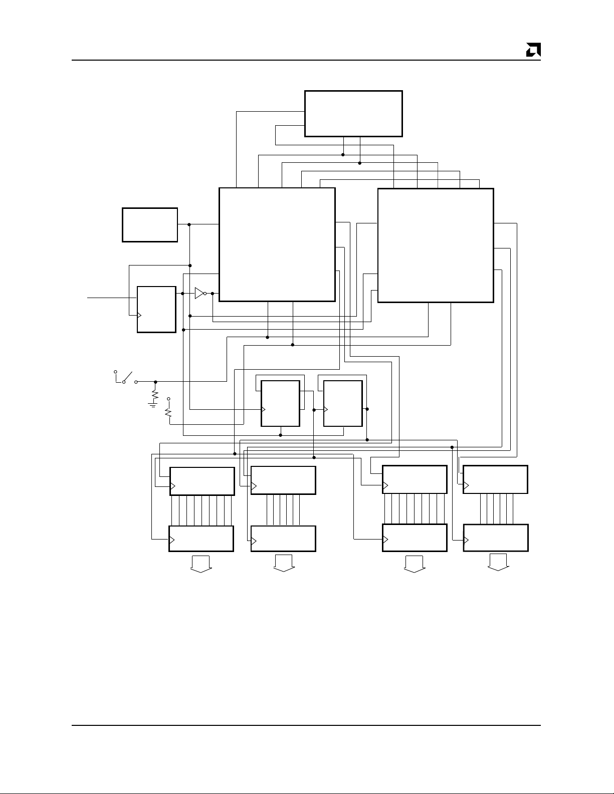
Implementing a 12-Port Unmanaged Hub
Both bIMR4 and bIMR8 chips have an expansion bus
that allows multiple devices to be connected together,
allowing high port count repeaters to be designed. The
operation of the expansion bus is identical for the bIMR4
and bIMR8. Minimum Mode is available in both bIMR4
and bIMR8 devices. This mode facilitates the
implementation of the LED display for unmanaged hub.
Figure 2 shows a simple example where one four port
bIMR device and one eight port bIMR device are connected together to form one twelve port logical
unmanaged repeater. As both devices are on the same
board the arbiter function can be local, and the bus
transceivers shown at right in Figure 1 are not
necessary due to the low bus loading in this example. In
this case, the arbiter simply asserts ACK if one REQ signal is asserted and COL if both REQ signals are asserted. The arbiter does not assert either signal if neither
REQ is asserted. Note that both ACK and COL are logic
low when asserted.
The D type flip flop is used to synchronize the reset
signals to both bIMR devices in order to ensure that the
internal 10 MHz clocks of these devices are in phase.
More complex repeaters, including stackable hubs, may
be built using the bIMR family. In these cases, the bus
transceivers may be necessary and the arbitration may
be distributed throughout the system.
1–16
Am79C982
ASYNC
RESET
20 MHz CLK
Q
D
Q
CK
CLR
PRELIMINARY
REQ1
REQ2
REQACKCOLDATJAM
X1
CRS
bIMR8
RST
TEST
SI SCLK
STR
SO
ARBITER
REQACKCOLDATJAM
X1
RST
TEST
bIMR4
SI SCLK
CRS
SO
STR
AMD
5 V
SW 1
5 V
SI
SHIFT REG
CK
CK
PORT STATUS LEDS
Q
D
Q
CK
CLR
SI
SHIFT REG
CK
CK
D
CK
CLR
Q
Q
SI
CK
CK CK
SI
SHIFT REGSHIFT REG
CK
PORT ACTIVITY LEDS
19406B-7
Notes:
1. Both bIMR8 and bIMR4 devices are used in Minimum Mode.
2. The information displayed by Port Status LEDs is selected by SW1. In this design, only Link Status and Port Partition Status can
be selected. Users can implement more display options by changing the state of the SCLK input (see the section on Minimum
Mode for detail).
3. The Polarity correction feature is shown disabled since the SI is high at reset. Users can enable this feature by keeping the SI
input low upon reset.
Figure 2. Implementing a 12-Port Unmanaged Hub using a bIMR8 and a bIMR4
Am79C982
1–17

AMD
PRELIMINARY
Management Port
The bIMR device management functions are enabled
when the TEST pin is tied LOW. The management commands are byte oriented data and are input serially on
the SI pin. Any responses generated during execution of
a management command are output serially in a byteoriented format by the bIMR device on the SO pin. Both
the input and output data streams are clocked with the
rising edge of the SCLK pin. The serial command data
stream and any associated results data stream are
structured in a manner similar to the RS232 serial data
format, i.e., one Start Bit followed by eight Data Bits.
The externally generated clock at the SCLK pin can be
either a free running clock synchronized to the input bit
patterns or a series of individual transitions meeting the
Command Execution Phase Results Phase
SCLK
setup and hold times with respect to the input bit pattern.
If the latter method is used, it is to be noted that 20 SCLK
clock transitions are required for proper execution of
management commands that produce SO data, and
that 14 SCLK clock transitions are needed to execute
management commands that do not produce SO data.
Management Commands
The following section details the operation of each management command available in the bIMR chip. In all
cases, the individual bits in each command byte are
shown with the MSB on the left and the LSB on the right.
Data bytes are received and transmitted LSB first and
MSB last. See Table 2 for a summary of the management commands.
Next Command
SO
SCLK
SO
SI
STRTD0 D1D2D3D4D5D6 D7
STRTD0 D1D2D3D4D5D6 D7
19406B-8
Management Command/Response Timing
Command Execution Phase Next Command Execution Phase
SI
STRTD0 D1D2D3D4D5D6 D7 STRTD0 D1D2D3D4D5D6 D7
19406B-9
Management Command Timing with No Response
1–18
Am79C982

PRELIMINARY
Table 2. Management Port Command Summary
Commands SI Data SO Data
Set (Write) Opcodes
bIMR Chip Programmable Options 0000 10SA
Alternate AUI Partitioning Algorithm 0001 1111
Alternate TP Partitioning Algorithm 0001 0000
AUI Port Disable 0010 1111
AUI Port Enable 0011 1111
TP Port Disable 0010 0### (note 2)
TP Port Enable 0011 0###
Disable Link Test Function (per TP port) 0100 0###
Enable Link Test Function (per TP port) 0101 0###
Disable Automatic Receiver Polarity Reversal (per TP port) 0110 0###
Enable Automatic Receiver Polarity Reversal (per TP port) 0111 0###
Get (Read) Opcodes
AUI Port Status (B, S, L Cleared) 1000 1111 PBSL 0000
TP Port Partitioning Status 1000 0000 C7...C0 (bIMR8),
C3...C0 (bIMR4)
Bit Rate Status of TP ports 1010 0000 E7...E0 (bIMR8),
E3...E0 (bIMR4)
Link Test Status of TP ports 1101 0000 L7...L0 (bIMR8),
L3...L0 (bIMR4)
Receive Polarity Status of all TP ports 1110 0000 P7...P0 (bIMR8),
P3...P0 (bIMR4)
MJLP Status 1111 0000 M000 0000
Version 1111 1111 XXXX 0101
AUI Port Status (S, L Cleared) 1000 1011 PBSL 0000
AUI Port Status (B Cleared) 1000 1101 PBSL 0000
AUI Port Status (None Cleared) 1000 1001 PBSL 0000
AMD
Notes:
1. Unused opcodes are reserved for future use.
2. Select code for the twisted pair ports (TP0 to TP7).
### bIMR8 bIMR4
000 TP0 —
001 TP1 TP0
010 TP2 —
011 TP3 TP1
100 TP4 —
101 TP5 TP2
110 TP6 —
111 TP7 TP3
Am79C982
1–19

AMD
PRELIMINARY
SET (Write) Opcodes
bIMR Chip Programmable Options
SI data: 0000 10SA
SO data: None
bIMR Chip Programmable Options can be enabled (dis-
abled) by setting (resetting) the appropriate bit in the
command string. The two programmable bits are:
S—AUI SQE Test Mask, and A—Alternative Port Activ-
ity Monitor (PAM) Function. These options can be enabled (disabled) by setting (resetting) the appropriate bit
in the command string.
S—AUI SQE Test Mask
Setting this bit allows the bIMR chip to ignore activity on
the CI signal pair, in the SQE Test Window, following a
transmission on the AUI port. This event occurs when
the attached MAU has the SQE Test option enabled,
therefore generating a burst of CI activity following every
transmission. This is interpreted by the bIMR device as
a collision, causing the bIMR device to generate a full
Jam pattern. Although the MAU attached to a repeater is
required not to have its SQE test function active, this is a
common installation error, causing difficulty in diagnosing network throughput problems.
The SQE Test Window, as defined by the IEEE 802.3
(Section 7.2.2.2.4), is from 6-bit times to 34-bit times
(0.6 µs to 3.4 µs). This includes delay introduced by a
50 m AUI. CI activity that occurs outside this window is
not ignored and is treated as true collision.
Note that enabling this function does not prevent the reporting of this condition by the bIMR device and the two
functions operate independently.
A—Alternative Port Activity Monitor (PAM)
Function
Setting the Alternative Port Activity Monitor Function allows the PAM function to be altered such that the Carrier
Sense data is presented unmodified. In default operation the PAM output (Carrier Sense bits in the CRS bit
stream) are masked if the port is either disabled or partitioned. This does not allow the Repeater Management
software to sense activity on all segments at all times.
The ability to monitor partitioned or disabled ports allows
fault tolerance to be built into the Repeater Management
software.
Alternate AUI Port Partitioning Algorithm
SI data: 00011111
SO data: None
The AUI port Partitioning/Reconnection scheme can be
programmed for the alternate (transmit only) reconnection algorithm by invoking this command. To return the
AUI back to the standard (transmit or receive) reconnection algorithm, it is necessary to reset the bIMR device.
Standard partitioning algorithm is selected upon reset.
Alternate TP Ports Partitioning Algorithm
SI data: 00010000
SO data: None
The TP ports Partitioning/Reconnection scheme can be
programmed for the alternate (transmit only) reconnection algorithm by invoking this command. All TP ports
are affected as a group by this command. To return the
TP ports back to the standard (transmit or receive) reconnection algorithm, it is necessary to reset the bIMR
device. The standard partitioning algorithm is selected
upon reset.
AUI Port Disable
SI data: 00101111
SO data: None
The AUI port will be disabled upon receiving this command. Subsequently, the bIMR chip will ignore all inputs
(Carrier Sense and SQE) appearing at the AUI port and
will not transmit any data or Jam Sequence on the AUI
port. Issuing this command will also cause the AUI port
to have its internal partitioning state machine forced to
its idle state. Therefore, a Partitioned Port may be reconnected by first disabling and then re-enabling
the port.
1–20
Am79C982

PRELIMINARY
AUI Port Enable
SI data: 00111111
SO data: None
This command enables a previously disabled AUI port.
Note that a partitioned AUI port may be reconnected by
first disabling (AUI Port Disable Command) and then reenabling the port with this command.
All ports are enabled upon reset.
TP Port Disable
SI data: 00100###
SO data: None
(### selects TP port number,
see note 2 on page 17)
The TP port designated in the command byte will be disabled upon receiving this command. Subsequently, the
bIMR device will ignore all inputs appearing at the disabled port’s receive pins and will not transmit any data or
JAM Sequence on that port’s transmit pins. Issuing this
command will also cause a TP port to have its partitioning state machine returned to its Idle State (Port Reconnected). Therefore, a partitioned port may be
reconnected by first disabling and then re-enabling the
port. The disabled port will continue to report correct
Link Test Status.
TP Port Enable
SI data: 00110###
SO data: None
(### selects TP port number,
see note 2 on page 17)
This command enables a previously disabled TP port.
Re-enabling a disabled port causes the port to be placed
into Link Test Fail state. This ensures that packet fragments received on the port are not repeated to the rest of
the network. Note that to force a TP port into the Link Fail
state and/or to reconnect a partitioned TP port, the port
should first be disabled (TP Port Disable Command)
and then re-enabled with this command. All ports are
enabled upon reset.
Disable Link Test Function of a TP Port
SI data: 01000###
SO data: None
(### selects TP port number,
see note 2 on page 17)
This command disables the Link Test Function at the TP
port designated in the command byte, i.e., the TP port
will no longer be disconnected due to Link Fail. A TP port
which has its Link Test Function disabled will continue to
transmit Link Test Pulses. If a twisted pair port has Link
Test disabled, then reading the Link Test Status indicates it being in Link Test Pass.
AMD
Enable Link Test Function of a TP Port
SI data: 01010###
SO data: None
(### selects TP port number,
see note 2 on page 17)
This command re-enables the Link Test Function in the
TP port designated in the command byte. This command executes only if the designated TP port has had
the Link Test Function disabled by the Disable Link Test
Function command. Otherwise, the command is ignored. Link Test is enabled upon reset.
Disable Automatic Receiver Polarity Reversal
SI data: 01100###
SO data: None
(### selects TP port number,
see note 2 on page 17)
This command disables the Automatic Receiver Polarity
Reversal Function for the TP port designated in the
command byte. If this function is disabled on a TP port
with reverse polarity (due to a wiring error), then the TP
port will fail Link Test due to the reversed polarity of the
Link Pulses. If the Link Test Function is also disabled on
the TP port, then the received reversed polarity packets
would be repeated to all other network ports in the bIMR
chip as inverted data. Automatic Polarity reversal is disabled upon reset.
Enable Automatic Receiver Polarity Reversal
SI data: 01110###
SO data: None
(### selects TP port number,
see note 2 on page 17)
This command enables the Automatic Receiver Polarity
Reversal Function for the TP port designated in the
command byte. If enabled in a TP port, the bIMR chip
will automatically invert the polarity of that TP port’s receiver circuitry if the TP port is detected as having reversed polarity (due to a wiring error). After reversing
the receiver polarity, the TP port could then receive subsequent (reverse polarity) packets correctly.
GET (Read) Opcodes
AUI Port Status
SI data: 10001111
SO data: PBSL0000
The combined AUI status allows a single instruction to
be used for monitoring AUI port. The four status bits reported are:
PPartitioning Status. This bit is 0 if the AUI port is
partitioned and 1 if connected.
Am79C982
1–21

AMD
PRELIMINARY
BBit Rate Error. This bit is set to 1 if there has been an
instance of FIFO Overflow or Underflow, caused by
data received at the AUI port. This bit is cleared when
the status is read.
SSQE Test Status. This bit is set to 1 if SQE Test is
detected by the bIMR chip. This bit is cleared when
the status is read. A MAU attached to a repeater
must have SQE Test disabled. This bit is set even if
the AUI port is disabled or partitioned.
LLoop Back Error. The MAU attached to the AUI is
required to loopback data transmitted to DO onto the
DI circuit. If loopback carrier is not detected by the
bIMR device, then this bit is set to 1 to report this
condition. This bit is cleared when the status is read.
For a repeater this is the only indication of a broken
or missing MAU.
TP Port Partitioning Status
SI data: 10000000
SO data: P7....................P0 (bIMR8)
SO data: P3 X P2 X P1 X P0 (bIMR4)
X = don’t care
Pn = 0 TP port n partitioned
Pn = 1 TP port n connected
Ln = 0 TP Port n in Link Test Fail
Ln = 1 TP Port n in Link Test Pass
The Link Test Status of all eight (four) TP ports are accessed by this command. A disabled port continues to
report correct Link Test Status. Re-enabling a disabled
port causes the port to be placed into Link Test Fail
state. This ensures that packet fragments received on
the port are not repeated to the rest of the network.
Receive Polarity Status of TP Ports
SI data: 11100000
SO data: P7....................P0 (bIMR8)
SO data: P3 X P2 X P1 X P0 (bIMR4)
X = don’t care
Pn = 0 TP Port n Polarity Correct
Pn = 1 TP Port n Polarity Reversed
The statuses of all eight (four) TP port polarities are accessed with this command. The bIMR chip has the ability to detect and correct reversed polarity on the TP
ports’ RXD+/– pins. If the polarity is detected as reversed for a TP port, then the bIMR chip will set the appropriate bit in this command’s result byte only if the
Polarity Reversal Function is enabled for that port.
The partitioning Status of all four or eight TP ports are
accessed by this command. If a port is disabled, reading
it partitioning status will indicate that it is connected.
Bit Rate Error Status of TP Ports
SI data: 10100000
SO data: E7....................E0 (bIMR8)
SO data: E3 X E2 X E1 X E0 (bIMR4)
X = don’t care
This allows a single command to be used to report Bit
Rate Error condition (FIFO Overflow or Underflow) of all
Twisted Pair ports. The 8 bits (4 bits) of the output pattern correspond to each of the 8 TP (4 TP) ports, with
least significant bit corresponding to port 0.
The status bit for a port is set to 1 if there has been an
instance when data received from that port has caused
a FIFO error.
All status bits stay set until the status is read.
Link Test Status of TP Ports
SI data: 11010000
SO data: L7....................L0 (bIMR8)
SO data: L3 X L2 X L1 X L0 (bIMR4)
X = don’t care
MJLP Status
SI data: 11110000
SO data: M00000000
Each bIMR chip contains an independent MAU Jabber
Lock Up Protection Timer. The timer is designed to inhibit the bIMR device transmit function, if it has been
transmitting continuously for more than 65536 Bit
Times. The MJLP Status bit (M) is set to 1 if this happens. This bit remains set and is only cleared when the
MJLP status is read by using this command.
Version
SI data: 11111111
SO data: XXXX0001
This command (1111 1111) can be used to determine
the device version.
The bIMR chip responds by the bit pattern:XXXX 0101
1–22
Am79C982

PRELIMINARY
Minimum Mode
The Minimum Mode reconfigures the bIMR device Management Port and is intended to provide support for the
low end, non-managed repeaters, requiring minimal external logic to provide LED indication of:
■Twisted Pair Ports Link Status indication and AUI
Loopback Status
■Port Partitioning Status
■Twisted Pair Ports Receiver Polarity Status and
AUI SQE Test Error Status
■Port Bit Rate Error Status
The Minimum Mode is selected by controlling the state
of the TEST pin while RST is asserted. If TEST is High
(asserted), while reset is active (RST LOW), then Minimum Mode is selected. The state of SI pin, at the deassertion of the RST signal, determines whether the
bIMR chip is to be programmed for Automatic Polarity
Detection/Correction.
When entering the Minimum Mode, the TEST input has
to be deasserted on the rising edge of reset. A maximum
delay of 100 ns is allowed to account for slow devices.
The following table summarizes the different modes
available.
Test SI Functions
0 0 Normal Management Mode
0 1 Normal Management Mode
1 0 Minimum Mode, Receive
Polarity Correction disabled
1 1 Minimum Mode, Receive
Polarity Correction enabled
AMD
In Minimum Mode, the SO pin is used to serially output
the various status information based on the state of the
SI and SCLK pins. A summary of the status information
is provided in the following table.
SCLK SI SO Output
0 0 TP Ports Receive Polarity Status +
AUI SQE Test Error Status.
0 1 Bit Rate Error (all ports).
1 0 TP Ports Link Status + AUI
LoopBack Status
1 1 Port Partitioning Status (all ports)
When SI = 0 then SO will output the related AUI status
bits (LoopBack or SQE), followed by the 8 (4) TP status
bits (Link or Polarity), starting with the TP port 0.
When SI = 1, the Port Partitioning Status or Port Bit Rate
Error Status are scanned out with the AUI first and TP
ports following. TP Port 0 is scanned out first.
Note that the Bit Rate Error, AUI Loopback, and AUI
SQE Test Error status bits stay set until they are
scanned out.
The state of SI and SCLK inputs is checked at the end of
every STR cycle. The rising edge of the X1 clock, occurring before falling edge of STR, is used to strobe in the
state of the SI and SCLK pins.
In this Minimum Mode, the Management Port mode is
not active. To exit the Minimum mode, the bIMR device
must reset into the normal Management Port mode.
ASYNC
RESET
XTAL
OSC
1/2 ’74
CK
D
1/2 ’74
QD
CK Q
CLR
X1
Am79C982
X2
bIMR8 Chip
Q
RST
TEST
SCLK SI
SO
STR
TCK
TCK
CK
SI
CK
T
P
7
Figure 3. bIMR8 LED Display Design using Minimum Mode
Am79C982
Register
T
T
P
P
5
6
SIPO
A
T
U
P
I
0
19406B-10
1–23

AMD
PRELIMINARY
X1
TCK
(Note 1)
CRS
SO
(Note 2)
CRS
AUI
SO
AUI
CRS
TP0
CRS
TP1
CRS
TP2
CRS
TP3
CRS
TP4
SO
TP0SOTP1SOTP2SOTP3SOTP4SOTP5SOTP6
STR
Notes:
1. Externally generated signal illustrates internal bIMR chip clock phase relationship.
2. For Minimum Mode
Figure 4. bIMR8 Management Port Minimum Mode and
Port Activity Monitor Signal Relationship
CRS
TP5
CRS
TP6
CRS
TP7
SO
TP7
CRS
AUI
SO
AUI
19406B-11
D
CK
CLR
Q
CK
Q
D
CLR
Q
Q
SHCK
XTAL
OSC
X1
CRS or
SO (Note)
CK
SI
Shift Register
bIMR4 Chip
CK
ASYNC
RESET
Q
Q
D
Note: When used in minimum mode.
RST
STR
CK
T
P
3
Register
T
T
P
P
1
2
T
P
0
A
U
I
19406B-12
Figure 5. bIMR4 LED Display Design using Minimum Mode
‘
1–24
Am79C982

PRELIMINARY
1 2 12 16 20
X1
RST
SHCK
CRS
SO
(Note)
STR
Note: When used in minimum mode.
AUI TP1TP0
AUI TP1TP0
24 28 3210
TP3TP2
TP3TP2
Figure 6. bIMR4 Management Port Minimum Mode and Port Activity Monitor Signal Relationship
Port Activity Monitor
Two pins, CRS and STR, are used to serially output the
state of the internal Carrier Sense signals from the AUI
and the eight (four) TP ports. This function together with
external hardware and/or software can be used to monitor repeater receive and/or collision activity.
The resolution of the CRS signal is 2 ms. The incoming
data is sampled repeatedly during each 2 ms period. If
any activity occurs (regardless of length) during any
2 ms period, this activity will be latched. At the start of
the next 2 ms period, the bIMR device will examine the
latches for each port. For any port in which activity
occurred, the corresponding bit in the CRS output
stream will remain set for the 2 ms period. This means
that during any 2 ms time interval the CRS output bit
stream represents carrier activity that occurred in the
preceding 2 ms period (see Figure 7). During the last
1000 ns of the 2 ms period, the CRS signal is reset to
LOW. Figure 7 illustrates this by showing the output of
the register in the recommended LED drive circuitry of
Figure 8.
The CRS pin is used to indicate carrier sense for all nine
ports of the device (five for the Am79C982-4). This pin
outputs a ten bit stream that repeats every microsecond.
During this period there are ten bit times (100 ns). Each
port has a “time slot” in this repeating bit stream (see
Figure 4). For example, activity on the AUI port is represented by the state of the CRS pin during the second
100 ns period of the one microsecond cycle.
Because the one microsecond sequence is repeated
unchanged for most of the longer 2 ms cycle, any LED
driven by the latch and shift register shown in Figure 3
and 5 will remain on for at least 2 ms. This minimizes the
need for external pulse stretching logic.
AMD
AUI
AUI
19406B-13
TPX
or AUI
2 ms
1000 ns
Figure 7. Carrier Sense Signal Output Corresponding to the
States of AUI or Twisted-Pair Port Activity
Am79C982
CRS
19406B-14
1–25

AMD
ASYNC
RESET
XTAL
OSC
1/2 ’74
CK
D
PRELIMINARY
1/2 ’74
QD
CK Q
CLR
X1
Am79C982
X2
bIMR8 Chip
Q
RST
CRS
STR
TCK
TCK
CK
SI
CK Register
T
T
P
P
6
7
Carrier Sense Outputs
Figure 8a. bIMR8 Port Activity Monitor Implementation
Shift Register
SIPO
T
P
5
T
P
0
A
U
I
19406B-15
1–26
Am79C982

APPENDIX
10BASE-T INTERFACE
A
The table below lists the recommended resistor values and filter and transformer modules for the IMR+ device.
bIMR+ Device Compatible 10BASE-T Media Interface Modules
¶ Manufacturer Part # Package Description
Bel Fuse S556-5999-32 16-pin SMD Transmit and receive filters, transformers and common mode chokes.
Bel Fuse 0556-2006-14 10-pin SIL Transmit and receive filters, transformers and common mode chokes.
Bel Fuse A556-2006-DE 16-pin 0.3" DIL Transmit and receive filters and transformers.
Bel Fuse
Halo Electronics FS02-101Y4 "Slim SIP" Transmit and receive filters and transformers.
Halo Electronics FS12-101Y4 "Slim SIP" Transmit and receive filters and transformers, transmit common mode reduction
Halo Electronics FS22-101Y4 "Slim SIP" Transmit and receive filters, transformers and common mode chokes.
Halo Electronics FD02-101G 16-pin 0.3" DIL Transmit and receive filters and transformers.
Halo Electronics FD12-101G 16-pin 0.3" DIL Transmit and receive filters and transformers, transmit common mode choke.
Halo Electronics FD22-101G 16-pin 0.3" DIL Transmit and receive filters, transformers and common mode chokes.
Halo Electronics FD22-101R2 16-pin 0.3" DIL Termination and equalization resistors, transmit and receive filters, transformers
Nano Pulse 5408-37 16-pin SMD 7 pole transmit and receive filters with 1CT:1CT Xfmrs (transmit & receive) and a
Nano Pulse 5408-40 9-pin SIP 7 pole transmit and receive filters with 1CT:1CT Xfmrs (transmit & receive) and a
Nano Pulse 6612-21 12-pin DIL 7 pole transmit and receive filters with 1CT:1CT Xfmrs (transmit & receive) and a
PCA Electronics EPA1990A 16-pin 0.3" DIL Transmit and receive filters and transformers.
PCA Electronics EPA1990AG SMT device Transmit and receive filters and transformers.
PCA Electronics EPA2013D 16-pin 0.3" DIL Transmit and receive filters and transformers, transmit common mode choke.
PCA Electronics EPA2013DG SMT device Transmit and receive filters and transformers, transmit common mode choke.
Pulse Engineering 78Z034C 16-pin DIL Transmit and receive filters and transformers, transmit common mode chokes.
Pulse Engineering 78Z1120B-01 16-pin DIL Transmit and receive filters and transformers.
Pulse Engineering 78Z1122B-01 16-pin DIL Transmit and receive filters, transformers and common mode chokes.
Pulse Engineering PE-68017S 10-pin SIL Transmit and receive filters, transformers and common mode chokes.
Pulse Engineering PE-68026 16-pin SMT Transmit and receive filters, transformers and common mode chokes.
Pulse Engineering PE-68056 16-pin SMT Transmit and receive filters, transformers and common mode chokes.
Pulse Engineering PE-68032 13-pin PCMCIA-SMT Transmit and receive filters and transformers, transmit common mode chokes.
TDK TLA-3M601-RS 10-pin SIP Transmit and receive filters and transformers, transmit common mode chokes.
TDK TLA-3M102(-T) 16-pin SMD Integrated resistors, transmit and receive filters and transformers, transmit common
TDK TLA-3M103(-T) 16-pin SMD Transmit and receive filters and transformers, transmit common mode chokes.
Valor Electronics PT3877 16-pin 0.3" DIL Transmit and receive filters and transformers.
Valor Electronics PT3983 8-pin 0.3" DIL Transmit and receive common mode chokes.
Valor Electronics FL1012 16-pin 0.3" DIL Transmit and receive filters and transformers, transmit common mode chokes.
A556-2006-00
16-pin DIL Transmit filter, transformers and common mode choke. Receive filter and
transformer.
choke.
and common mode chokes.
separate common mode choke for each channel.
separate common mode choke for each channel.
separate common mode choke for each channel.
mode chokes.
Am79C982 1-27

APPENDIX B
Glossary
Active Status
In a non-collision state, a bIMR chip is considered active
if it is receiving data on any one of its network ports, or is
in the process of broadcasting (repeating) FIFO data
from a recently completed data reception. In a collision
state (the bIMR device is generating Jam Sequence), an
bIMR device is considered active if any one or more network ports is receiving data. The bIMR device asserts
the REQ line to indicate that it is active.
Collision
In a carrier sense multiple access/collision detection
(CSMA/CD) network such as Ethernet, only one node
can successfully transfer data at any one time. When
two or more separate nodes (DTEs or repeaters) are simultaneously transmitting data onto the network, a Collision state exists. In a repeater using one or more bIMR
devices, a Collision state exists when more than one
network port is receiving data at any instant, or when
any one or more network ports receives data while the
bIMR device is transmitting (repeating) data, or when
the CI+/- pins become active (nominal 10 MHz signal)
on the AUI port.
Jam Sequence
A signal consisting of alternating 1s and 0s that is generated by the bIMR device when a Collision state is detected. This signal is transmitted by the bIMR device to
indicate to the network that one or more network ports in
the repeater is involved in a collision.
Network Port
Any of the eight (four) 10BASE-T ports or the AUI port
present in the bIMR device (i.e. not the Expansion Port
or the Management Port).
Partitioning
A network port on a repeater has been partitioned if the
repeater has internally ‘disconnected’ it from the repeater due to localized faults that would otherwise bring the
entire network down. These faults are generally cable
shorts and opens that tend to cause excessive collisions
at the network ports. The partitioned network port will be
internally re-connected if the network port starts behaving correctly again, usually when successful ‘collisionless’ transmissions and/or receptions resume.
Receive Collision
A network port is in a Receive Collision state when it detects collision and is not one of the colliding network
’nodes’. This applies mainly to a non-transmitting AUI
port because a remote collision is clearly identified by
the presence of a nominal 10 MHz signal on the CI+/pins. However, any repeater port would be considered
to be in a receive collision state if the repeater unit is receiving data from that port as the ‘one-port-left’ in the
collision sequence.
Transmit Collision
A network port is in a Transmit Collision state when collision occurs while that port is transmitting. On the AUI
port, Transmit Collision is indicated by the presence of a
nominal 10 MHz signal on the CI+/- pins while the AUI
port is transmitting on the DO+/- pins. On a 10BASE-T
port, Transmit Collision occurs when incoming data appears on the RXD+/- pins while the 10BASE-T port is
transmitting on the TXD+/- and TXP+/- pins.
1–28 Am79C982
 Loading...