


PRELIMINARY
Am79C974
PCnetTM-SCSI Combination Ethernet and SCSI Controller
for PCI Systems
DISTINCTIVE CHARACTERISTICS
PCI Features
■ Direct glueless interface to 33 MHz, 32-bit PCI
local bus
■ 132 Mbyte/s burst DMA transfer rate
■ Compliant to PCI local bus Specification
Revision 2.0
Ethernet Features
■ Supports ISO 8802-3 (IEEE/ANSI 802.3) and
Ethernet Standards
■ High-performance Bus Master architecture with
integrated DMA Buffer Management Unit for
low CPU and bus utilization
■ Individual 136-byte transmit and 128-byte
receive FIFOs provide frame buffering for
increased system latency
■ Microwire
jumperless design
■ Integrated Manchester Encoder/Decoder
■ Provides integrated Attachment Unit Interface
(AUI) and 10BASE-T transceiver with automatic
port selection
■ Automatic Twisted-Pair receive polarity detec-
tion and automatic correction of the receive
polarity
■ Dynamic transmit FCS generation programma-
ble on a frame-by-frame basis
■ Internal/external loopback capabilities
■ Supports the following types of network
interfaces:
— AUI to external 10BASE2, 10BASE5,
10BASE-T or 10BASE-F MAU
— Internal 10BASE-T transceiver with Smart
Squelch to Twisted-Pair medium
TM
EEPROM interface supports
SCSI Features
■ Compliant to ANSI standards X3.131 – 1986
(SCSI-1) and X3.131 – 199X (SCSI-2)
■ Fast 8-bit SCSI-2 10 Mbyte/s synchronous or
7Mbyte/s asynchronous data transfer rate
■ SCSI specific Bus Mastering DMA engine
(32-bit address/data)
■ 96-byte DMA FIFO for low bus latency
■ On-chip state machine to control the SCSI
sequences in hardware
■ Integrated industry standard Fast SCSI-2 core
■ Single-Ended 48 mA outputs to drive the SCSI
bus directly
■ Support for Scatter-Gather DMA data transfers
■ Hooks in silicon and software to enable disk
drive spin down for power savings
General Features
■ Software compatible with AMD’s Am79C960
PCnet-ISA, Am79C961 PCnet-ISA+, Am79C965
PCnet-32, Am79C970 PCnet-PCI register and
descriptor architecture
■ Plug-in and software compatible with AMD’s
PC
SCSI family of SCSI controllers for PCI
■ NAND Tree test mode for connectivity testing
on printed circuit boards
■ Single +5 V power supply operation
■ Low-power, CMOS design with sleep modes for
both Ethernet and SCSI controllers allows reduced power consumption for critical battery
powered applications and ‘Green PCs’
■ Fully static design for low frequency and
power operation
■ 132-pin PQFP package
Advanced
Micro
Devices
GENERAL DESCRIPTION
The PCnet-SCSI combination Ethernet and 8-bit Fast
SCSI controller with a 32-bit PCI bus interface is a highly
integrated Ethernet-Fast SCSI system solution designed to address high-performance system application
requirements. This single-chip is a flexible bus-mastering device that can be used in many applications, including network- and SCSI-ready PCs, printers, fax
This document contains information on a product under development at Advanced Micro Devices, Inc. The information is intended
to help you to evaluate this product. AMD reserves the right to change or discontinue work on this proposed product without notice.
modems, and bridge/router designs. The bus-master
architecture provides high data throughput in the system and low CPU and system bus utilization. The
PCnet-SCSI controller is fabricated with AMD’s advanced low-power CMOS process to provide low operating and standby current for power sensitive
applications.
Publication# 18681 Rev. B Amendment/1
Issue Date: October 1994

AMD
P R E L I M I N A R Y
The PCnet-SCSI is part of AMD’s PCI product family of
plug-in and software compatible SCSI and Ethernet
controllers. This product compatibility ensures a low
cost system upgrade path and lower motherboard
manufacturing costs.
Ethernet Specific
The PCnet-SCSI controller includes a complete Ethernet node integrated into a single VLSI device. It contains
a bus interface unit, a DMA buffer management unit, an
IEEE 802.3-defined Media Access Control (MAC) function, individual 136-byte transmit and 128-byte receive
FIFOs, an IEEE 802.3-defined Attachment Unit Interface (AUI) and Twisted-Pair Transceiver Media Attachment Unit (10BASE-T MAU), and a Microwire EEPROM
interface. The PCnet-SCSI controller is also register
compatible with the LANCE (Am7990) Ethernet controller, the C-LANCE (Am79C90) Ethernet controller, the
ILACC (Am79C900) Ethernet controller, and all Ethernet controllers in the PCnet Family, including the PCnetISA controller (Am79C960), the PCnet-ISA+ controller
(Am79C961), and the PCnet-32 controller
(Am79C965). The buffer management unit supports the
LANCE, ILACC, and PCnet descriptor software models.
The PCnet-SCSI controller is software compatible with
the Novell NE2100 and NE1500 Ethernet adapter card
architectures. In addition, a Sleep function has been incorporated to provide low standby current, excellent for
notebooks and Green PCs.
The 32-bit multiplexed bus interface unit provides a direct interface to the PCI local bus applications, simplifying the design of an Ethernet node in a PC system. With
its built-in support for both little and big endian byte
alignment, this controller also addresses proprietary
non-PC applications.
The PCnet-SCSI controller supports auto configuration
in the PCI configuration space. Additional PCnet-SCSI
controller configuration parameters, including the
unique IEEE physical address, can be read from an external non-volatile memory (serial EEPROM) immediately following system RESET.
The controller also has the capability to automatically
select either the AUI port or the Twisted-Pair transceiver. Only one interface is active at any one time. The
individual transmit and receive FIFOs optimize system
overhead, providing sufficient latency during frame
transmission and reception, and minimizing intervention
during normal network error recovery. The integrated
Manchester encoder/decoder (MENDEC) eliminates
the need for an external Serial Interface Adapter (SIA) in
the system. In addition, the device provides programmable on-chip LED drivers for transmit, receive, collision, receive polarity, link integrity or jabber status.
SCSI Specific
The PCnet-SCSI controller also includes a highperformance Fast SCSI controller with a glueless interface to the PCI local bus. The PCnet-SCSI integrates its
own 32-bit bus mastering DMA engine with an industry
standard Fast SCSI-2 block. The DMA engine and accompanying 96 byte DMA FIFO allow 32-bit burst data
transfers across the high bandwidth PCI bus at speeds
of up to 132 Mbyte/s. Full support for scatter-gather
DMA transfers optimize performance in multi-tasking
system applications.
The PCnet-SCSI’s on-chip state machine controls SCSI
bus sequences in hardware and is coupled with the bus
mastering DMA engine to eliminate the need for an onchip RISC processor. This results in a smaller die size
giving the Am79C974 superior price/performance versus competitive offerings.
AMD supports the Am79C974 with a total system solution which includes:
A full suite of licensable SCSI drivers and utilities
fully tested under the following operating system
environments:
— DOS 5.0 – 6.0
— Windows 3.1
— Windows NT
— OS/2 2.x
— Netware 3.x, 4.x
— SCO UNIX 3.2.4, ODT 2.0
An INT13h Compatible SCSI ROM BIOS
ASPI Compatibility
Complete hardware reference design kit
For more detailed information on the PCnet-SCSI refer
to the technical manual, PID #18738A.
2
Am79C974

HIGH LEVEL BLOCK DIAGRAM
SCSI Data SCSI Control 10Base-T, AUI Ports
SCSI Sequences,
SCSI Control,
SCSI Registers
P R E L I M I N A R Y
AMD
802.3 MAC Core
SCSI FIFO DMA Registers
DMA
FIFO
96 Bytes
PCI Data/Address PCI Host Control
FIFO &
DMA Control
PCI Host Control and Interface
RCV
FIFO
FIFO
Control
DMA Registers
DMA Control
XMT
FIFO
18681A-1
3Am79C974

AMD
CPU
Cache
SRAM
Control
Address
Data
P R E L I M I N A R Y
DRAM
Memory
Core
Logic
PC-AT ISA Bus
PCnet-SCSI
(Am79C974)
PCI Bus
Video
Control
PCI
to
ISA
Super I/O
IDE/Floppy
Ser/Par
Am79C974 in a PCI System
Keyboard
Control
18681A-2
4
Am79C974

P R E L I M I N A R Y
TABLE OF CONTENTS
DISTINCTIVE CHARACTERISTICS 1. . . . . . . . . . . . . . . . . . . . . . . . . . . . . . . . . . . . . . . . . . . . . .
GENERAL DESCRIPTION 1. . . . . . . . . . . . . . . . . . . . . . . . . . . . . . . . . . . . . . . . . . . . . . . . . . . . .
HIGH LEVEL BLOCK DIAGRAM 3. . . . . . . . . . . . . . . . . . . . . . . . . . . . . . . . . . . . . . . . . . . . . . . .
RELATED PRODUCTS 11. . . . . . . . . . . . . . . . . . . . . . . . . . . . . . . . . . . . . . . . . . . . . . . . . . . . . . .
CONNECTION DIAGRAM 12. . . . . . . . . . . . . . . . . . . . . . . . . . . . . . . . . . . . . . . . . . . . . . . . . . . . .
ORDERING INFORMATION 13. . . . . . . . . . . . . . . . . . . . . . . . . . . . . . . . . . . . . . . . . . . . . . . . . . .
PIN DESIGNATIONS 14. . . . . . . . . . . . . . . . . . . . . . . . . . . . . . . . . . . . . . . . . . . . . . . . . . . . . . . . .
Listed By Pin Number 14. . . . . . . . . . . . . . . . . . . . . . . . . . . . . . . . . . . . . . . . . . . . . . . . . . . . . .
Listed By Pin Name 15. . . . . . . . . . . . . . . . . . . . . . . . . . . . . . . . . . . . . . . . . . . . . . . . . . . . . . .
Quick Reference Pin Description 16. . . . . . . . . . . . . . . . . . . . . . . . . . . . . . . . . . . . . . . . . . . . .
Listed By Driver Type 17. . . . . . . . . . . . . . . . . . . . . . . . . . . . . . . . . . . . . . . . . . . . . . . . . . . . . .
LOGIC SYMBOL 18. . . . . . . . . . . . . . . . . . . . . . . . . . . . . . . . . . . . . . . . . . . . . . . . . . . . . . . . . . . .
PIN DESCRIPTION 19. . . . . . . . . . . . . . . . . . . . . . . . . . . . . . . . . . . . . . . . . . . . . . . . . . . . . . . . . .
PCI Bus Interface 19. . . . . . . . . . . . . . . . . . . . . . . . . . . . . . . . . . . . . . . . . . . . . . . . . . . . . . . . .
Ethernet Controller Pins 22. . . . . . . . . . . . . . . . . . . . . . . . . . . . . . . . . . . . . . . . . . . . . . . . . . . .
Board Interface 22. . . . . . . . . . . . . . . . . . . . . . . . . . . . . . . . . . . . . . . . . . . . . . . . . . . . . . . .
Microwire EEPROM Interface 23. . . . . . . . . . . . . . . . . . . . . . . . . . . . . . . . . . . . . . . . . . . . .
Attachment Unit Interface 24. . . . . . . . . . . . . . . . . . . . . . . . . . . . . . . . . . . . . . . . . . . . . . . .
Twisted-Pair Interface 24. . . . . . . . . . . . . . . . . . . . . . . . . . . . . . . . . . . . . . . . . . . . . . . . . . .
SCSI Controller Pins 24. . . . . . . . . . . . . . . . . . . . . . . . . . . . . . . . . . . . . . . . . . . . . . . . . . . . . . .
Test Interface 25. . . . . . . . . . . . . . . . . . . . . . . . . . . . . . . . . . . . . . . . . . . . . . . . . . . . . . . . . . . .
Miscellaneous 25. . . . . . . . . . . . . . . . . . . . . . . . . . . . . . . . . . . . . . . . . . . . . . . . . . . . . . . . . . . .
Power Supply 25. . . . . . . . . . . . . . . . . . . . . . . . . . . . . . . . . . . . . . . . . . . . . . . . . . . . . . . . . . . .
BASIC FUNCTIONS 26. . . . . . . . . . . . . . . . . . . . . . . . . . . . . . . . . . . . . . . . . . . . . . . . . . . . . . . . .
System Bus Interface Function 26. . . . . . . . . . . . . . . . . . . . . . . . . . . . . . . . . . . . . . . . . . . . . . .
Software Interface 26. . . . . . . . . . . . . . . . . . . . . . . . . . . . . . . . . . . . . . . . . . . . . . . . . . . . . . . . .
Ethernet Interfaces 26. . . . . . . . . . . . . . . . . . . . . . . . . . . . . . . . . . . . . . . . . . . . . . . . . . . . . . . .
SCSI Interfaces 26. . . . . . . . . . . . . . . . . . . . . . . . . . . . . . . . . . . . . . . . . . . . . . . . . . . . . . . . . . .
DETAILED FUNCTIONS 27. . . . . . . . . . . . . . . . . . . . . . . . . . . . . . . . . . . . . . . . . . . . . . . . . . . . . .
Bus Interface Unit (BIU) 27. . . . . . . . . . . . . . . . . . . . . . . . . . . . . . . . . . . . . . . . . . . . . . . . . . . .
Slave Configuration Transfers 27. . . . . . . . . . . . . . . . . . . . . . . . . . . . . . . . . . . . . . . . . . . . .
Slave I/O Transfers 29. . . . . . . . . . . . . . . . . . . . . . . . . . . . . . . . . . . . . . . . . . . . . . . . . . . . .
Bus Acquisition 31. . . . . . . . . . . . . . . . . . . . . . . . . . . . . . . . . . . . . . . . . . . . . . . . . . . . . . . .
Bus Master DMA Transfers 32. . . . . . . . . . . . . . . . . . . . . . . . . . . . . . . . . . . . . . . . . . . . . . .
Target Initiated Termination 37. . . . . . . . . . . . . . . . . . . . . . . . . . . . . . . . . . . . . . . . . . . . . . .
Master Initiated Termination 40. . . . . . . . . . . . . . . . . . . . . . . . . . . . . . . . . . . . . . . . . . . . . .
Ethernet Controller 43. . . . . . . . . . . . . . . . . . . . . . . . . . . . . . . . . . . . . . . . . . . . . . . . . . . . . . . .
Buffer Management Unit (BMU) 43. . . . . . . . . . . . . . . . . . . . . . . . . . . . . . . . . . . . . . . . . . . . . .
Initialization 43. . . . . . . . . . . . . . . . . . . . . . . . . . . . . . . . . . . . . . . . . . . . . . . . . . . . . . . . . . .
Re-Initialization 43. . . . . . . . . . . . . . . . . . . . . . . . . . . . . . . . . . . . . . . . . . . . . . . . . . . . . . . .
Buffer Management 43. . . . . . . . . . . . . . . . . . . . . . . . . . . . . . . . . . . . . . . . . . . . . . . . . . . . .
Descriptor Rings 43. . . . . . . . . . . . . . . . . . . . . . . . . . . . . . . . . . . . . . . . . . . . . . . . . . . . . . .
Descriptor Ring Access Mechanism 44. . . . . . . . . . . . . . . . . . . . . . . . . . . . . . . . . . . . . . . .
Polling 46. . . . . . . . . . . . . . . . . . . . . . . . . . . . . . . . . . . . . . . . . . . . . . . . . . . . . . . . . . . . . . .
Transmit Descriptor Table Entry (TDTE) 46. . . . . . . . . . . . . . . . . . . . . . . . . . . . . . . . . . . . .
Receive Descriptor Table Entry (RDTE) 48. . . . . . . . . . . . . . . . . . . . . . . . . . . . . . . . . . . . .
AMD
5Am79C974

AMD
P R E L I M I N A R Y
Media Access Control 48. . . . . . . . . . . . . . . . . . . . . . . . . . . . . . . . . . . . . . . . . . . . . . . . . . . . . .
Transmit and Receive Message Data Encapsulation 48. . . . . . . . . . . . . . . . . . . . . . . . . . .
Media Access Management 50. . . . . . . . . . . . . . . . . . . . . . . . . . . . . . . . . . . . . . . . . . . . . . .
Manchester Encoder/Decoder (MENDEC) 52. . . . . . . . . . . . . . . . . . . . . . . . . . . . . . . . . . . . . .
External Crystal Characteristics 52. . . . . . . . . . . . . . . . . . . . . . . . . . . . . . . . . . . . . . . . . . . .
External Clock Drive Characteristics 52. . . . . . . . . . . . . . . . . . . . . . . . . . . . . . . . . . . . . . . .
MENDEC Transmit Path 52. . . . . . . . . . . . . . . . . . . . . . . . . . . . . . . . . . . . . . . . . . . . . . . . .
Transmitter Timing and Operation 52. . . . . . . . . . . . . . . . . . . . . . . . . . . . . . . . . . . . . . . . . .
Receiver Path 53. . . . . . . . . . . . . . . . . . . . . . . . . . . . . . . . . . . . . . . . . . . . . . . . . . . . . . . . .
Input Signal Conditioning 53. . . . . . . . . . . . . . . . . . . . . . . . . . . . . . . . . . . . . . . . . . . . . . . . .
Clock Acquisition 53. . . . . . . . . . . . . . . . . . . . . . . . . . . . . . . . . . . . . . . . . . . . . . . . . . . . . . .
PLL Tracking 54. . . . . . . . . . . . . . . . . . . . . . . . . . . . . . . . . . . . . . . . . . . . . . . . . . . . . . . . . .
Carrier Tracking and End of Message 54. . . . . . . . . . . . . . . . . . . . . . . . . . . . . . . . . . . . . . .
Data Decoding 54. . . . . . . . . . . . . . . . . . . . . . . . . . . . . . . . . . . . . . . . . . . . . . . . . . . . . . . . .
Differential Input Terminations 54. . . . . . . . . . . . . . . . . . . . . . . . . . . . . . . . . . . . . . . . . . . . .
Collision Detection 55. . . . . . . . . . . . . . . . . . . . . . . . . . . . . . . . . . . . . . . . . . . . . . . . . . . . . .
Jitter Tolerance Definition 55. . . . . . . . . . . . . . . . . . . . . . . . . . . . . . . . . . . . . . . . . . . . . . . .
Attachment Unit Interface (AUI) 55. . . . . . . . . . . . . . . . . . . . . . . . . . . . . . . . . . . . . . . . . . . .
Twisted-Pair Transceiver (T-MAU) 55. . . . . . . . . . . . . . . . . . . . . . . . . . . . . . . . . . . . . . . . . . . .
Twisted-Pair Transmit Function 55. . . . . . . . . . . . . . . . . . . . . . . . . . . . . . . . . . . . . . . . . . . .
Twisted-Pair Receive Function 55. . . . . . . . . . . . . . . . . . . . . . . . . . . . . . . . . . . . . . . . . . . .
Link Test Function 56. . . . . . . . . . . . . . . . . . . . . . . . . . . . . . . . . . . . . . . . . . . . . . . . . . . . . .
Polarity Detection and Reversal 56. . . . . . . . . . . . . . . . . . . . . . . . . . . . . . . . . . . . . . . . . . . .
Twisted-Pair Interface Status 56. . . . . . . . . . . . . . . . . . . . . . . . . . . . . . . . . . . . . . . . . . . . . .
Collision Detect Function 57. . . . . . . . . . . . . . . . . . . . . . . . . . . . . . . . . . . . . . . . . . . . . . . . .
Signal Quality Error (SQE) Test (Heartbeat) Function 57. . . . . . . . . . . . . . . . . . . . . . . . . . .
Jabber Function 57. . . . . . . . . . . . . . . . . . . . . . . . . . . . . . . . . . . . . . . . . . . . . . . . . . . . . . . .
Power Down 57. . . . . . . . . . . . . . . . . . . . . . . . . . . . . . . . . . . . . . . . . . . . . . . . . . . . . . . . . .
10BASE-T Interface Connection 57. . . . . . . . . . . . . . . . . . . . . . . . . . . . . . . . . . . . . . . . . . .
Ethernet Power Savings Modes 58. . . . . . . . . . . . . . . . . . . . . . . . . . . . . . . . . . . . . . . . . . . . . .
Software Access 58. . . . . . . . . . . . . . . . . . . . . . . . . . . . . . . . . . . . . . . . . . . . . . . . . . . . . . . . . .
Ethernet PCI Configuration Registers 58. . . . . . . . . . . . . . . . . . . . . . . . . . . . . . . . . . . . . . .
I/O Resources 59. . . . . . . . . . . . . . . . . . . . . . . . . . . . . . . . . . . . . . . . . . . . . . . . . . . . . . . . .
I/O Register Access 61. . . . . . . . . . . . . . . . . . . . . . . . . . . . . . . . . . . . . . . . . . . . . . . . . . . . .
Hardware Access 64. . . . . . . . . . . . . . . . . . . . . . . . . . . . . . . . . . . . . . . . . . . . . . . . . . . . . . . . .
PCnet-SCSI Controller Master Accesses 64. . . . . . . . . . . . . . . . . . . . . . . . . . . . . . . . . . . .
Slave Access to I/O Resources 64. . . . . . . . . . . . . . . . . . . . . . . . . . . . . . . . . . . . . . . . . . . .
EEPROM Microwire Access 66. . . . . . . . . . . . . . . . . . . . . . . . . . . . . . . . . . . . . . . . . . . . . .
Transmit Operation 69. . . . . . . . . . . . . . . . . . . . . . . . . . . . . . . . . . . . . . . . . . . . . . . . . . . . . . . .
Transmit Function Programming 69. . . . . . . . . . . . . . . . . . . . . . . . . . . . . . . . . . . . . . . . . . .
Automatic Pad Generation 69. . . . . . . . . . . . . . . . . . . . . . . . . . . . . . . . . . . . . . . . . . . . . . . .
Transmit FCS Generation 70. . . . . . . . . . . . . . . . . . . . . . . . . . . . . . . . . . . . . . . . . . . . . . . .
Transmit Exception Conditions 70. . . . . . . . . . . . . . . . . . . . . . . . . . . . . . . . . . . . . . . . . . . .
Receive Operation 71. . . . . . . . . . . . . . . . . . . . . . . . . . . . . . . . . . . . . . . . . . . . . . . . . . . . . . . .
Receive Function Programming 71. . . . . . . . . . . . . . . . . . . . . . . . . . . . . . . . . . . . . . . . . . . .
Automatic Pad Stripping 71. . . . . . . . . . . . . . . . . . . . . . . . . . . . . . . . . . . . . . . . . . . . . . . . .
Receive FCS Checking 72. . . . . . . . . . . . . . . . . . . . . . . . . . . . . . . . . . . . . . . . . . . . . . . . . .
Receive Exception Conditions 72. . . . . . . . . . . . . . . . . . . . . . . . . . . . . . . . . . . . . . . . . . . . .
Loopback Operation 72. . . . . . . . . . . . . . . . . . . . . . . . . . . . . . . . . . . . . . . . . . . . . . . . . . . . . . .
LED Support 73. . . . . . . . . . . . . . . . . . . . . . . . . . . . . . . . . . . . . . . . . . . . . . . . . . . . . . . . . . . . .
6
Am79C974

P R E L I M I N A R Y
H_RESET, S_RESET, and STOP 74. . . . . . . . . . . . . . . . . . . . . . . . . . . . . . . . . . . . . . . . . . . .
H_RESET 74. . . . . . . . . . . . . . . . . . . . . . . . . . . . . . . . . . . . . . . . . . . . . . . . . . . . . . . . . . . .
S_RESET 74. . . . . . . . . . . . . . . . . . . . . . . . . . . . . . . . . . . . . . . . . . . . . . . . . . . . . . . . . . . .
STOP 74. . . . . . . . . . . . . . . . . . . . . . . . . . . . . . . . . . . . . . . . . . . . . . . . . . . . . . . . . . . . . . . .
SCSI Controller 75. . . . . . . . . . . . . . . . . . . . . . . . . . . . . . . . . . . . . . . . . . . . . . . . . . . . . . . . . . .
SCSI Specific DMA Engine 75. . . . . . . . . . . . . . . . . . . . . . . . . . . . . . . . . . . . . . . . . . . . . . . . . .
DMA FIFO 76. . . . . . . . . . . . . . . . . . . . . . . . . . . . . . . . . . . . . . . . . . . . . . . . . . . . . . . . . . . .
DMA Blast Command 76. . . . . . . . . . . . . . . . . . . . . . . . . . . . . . . . . . . . . . . . . . . . . . . . . . .
Funneling Logic 76. . . . . . . . . . . . . . . . . . . . . . . . . . . . . . . . . . . . . . . . . . . . . . . . . . . . . . . .
SCSI DMA Programming Sequence 76. . . . . . . . . . . . . . . . . . . . . . . . . . . . . . . . . . . . . . . .
MDL Based DMA Programming 76. . . . . . . . . . . . . . . . . . . . . . . . . . . . . . . . . . . . . . . . . . . .
DMA Scatter-Gather Mechanism 78. . . . . . . . . . . . . . . . . . . . . . . . . . . . . . . . . . . . . . . . . . .
Memory Descriptor List (MDL) 78. . . . . . . . . . . . . . . . . . . . . . . . . . . . . . . . . . . . . . . . . .
DMA Scatter-Gather Operation (4k aligned elements) 78. . . . . . . . . . . . . . . . . . . . . . . .
DMA Scatter-Gather Operation (Non-4k aligned elements MDL not set) 80. . . . . . . . . .
Interrupts 81. . . . . . . . . . . . . . . . . . . . . . . . . . . . . . . . . . . . . . . . . . . . . . . . . . . . . . . . . . . . .
The Fast SCSI Block 81. . . . . . . . . . . . . . . . . . . . . . . . . . . . . . . . . . . . . . . . . . . . . . . . . . . . . . .
SCSI Block ID 81. . . . . . . . . . . . . . . . . . . . . . . . . . . . . . . . . . . . . . . . . . . . . . . . . . . . . . . . .
SCSI FIFO Threshold 81. . . . . . . . . . . . . . . . . . . . . . . . . . . . . . . . . . . . . . . . . . . . . . . . . . .
Data Transmission 81. . . . . . . . . . . . . . . . . . . . . . . . . . . . . . . . . . . . . . . . . . . . . . . . . . . . . .
REQ/ACK Control 81. . . . . . . . . . . . . . . . . . . . . . . . . . . . . . . . . . . . . . . . . . . . . . . . . . . . . .
Parity 82. . . . . . . . . . . . . . . . . . . . . . . . . . . . . . . . . . . . . . . . . . . . . . . . . . . . . . . . . . . . . . . .
Parity Checking on the SCSI Bus 82. . . . . . . . . . . . . . . . . . . . . . . . . . . . . . . . . . . . . . . .
Parity Generating on the SCSI Bus 82. . . . . . . . . . . . . . . . . . . . . . . . . . . . . . . . . . . . . .
Reset Levels 82. . . . . . . . . . . . . . . . . . . . . . . . . . . . . . . . . . . . . . . . . . . . . . . . . . . . . . . . . .
Hard Reset: (H) 82. . . . . . . . . . . . . . . . . . . . . . . . . . . . . . . . . . . . . . . . . . . . . . . . . . . . .
Soft Reset: (S) 82. . . . . . . . . . . . . . . . . . . . . . . . . . . . . . . . . . . . . . . . . . . . . . . . . . . . . .
Disconnected Reset: (D) 83. . . . . . . . . . . . . . . . . . . . . . . . . . . . . . . . . . . . . . . . . . . . . .
Device Commands 83. . . . . . . . . . . . . . . . . . . . . . . . . . . . . . . . . . . . . . . . . . . . . . . . . . . . . .
Command Stacking 84. . . . . . . . . . . . . . . . . . . . . . . . . . . . . . . . . . . . . . . . . . . . . . . . . .
Invalid Commands 84. . . . . . . . . . . . . . . . . . . . . . . . . . . . . . . . . . . . . . . . . . . . . . . . . . .
Command Window 84. . . . . . . . . . . . . . . . . . . . . . . . . . . . . . . . . . . . . . . . . . . . . . . . . . .
Initiator Commands 84. . . . . . . . . . . . . . . . . . . . . . . . . . . . . . . . . . . . . . . . . . . . . . . . . .
Information Transfer Command 84. . . . . . . . . . . . . . . . . . . . . . . . . . . . . . . . . . . . . . .
Initiator Command Complete Steps 85. . . . . . . . . . . . . . . . . . . . . . . . . . . . . . . . . . . .
Message Accepted Command 85. . . . . . . . . . . . . . . . . . . . . . . . . . . . . . . . . . . . . . .
Transfer Pad Bytes Command 85. . . . . . . . . . . . . . . . . . . . . . . . . . . . . . . . . . . . . . .
Set ATN Command 85. . . . . . . . . . . . . . . . . . . . . . . . . . . . . . . . . . . . . . . . . . . . . . . .
Reset ATN Command 86. . . . . . . . . . . . . . . . . . . . . . . . . . . . . . . . . . . . . . . . . . . . . .
Idle State Commands 86. . . . . . . . . . . . . . . . . . . . . . . . . . . . . . . . . . . . . . . . . . . . . . . . .
Select Without ATN Steps Command 86. . . . . . . . . . . . . . . . . . . . . . . . . . . . . . . . . .
Select With ATN Steps Command 86. . . . . . . . . . . . . . . . . . . . . . . . . . . . . . . . . . . .
Select With ATN and Stop Steps Command 86. . . . . . . . . . . . . . . . . . . . . . . . . . . . .
Enable Selection/Reselection Command 86. . . . . . . . . . . . . . . . . . . . . . . . . . . . . . .
Disable Selection/Reselection Command 87. . . . . . . . . . . . . . . . . . . . . . . . . . . . . . .
Select With ATN3 Steps Command 87. . . . . . . . . . . . . . . . . . . . . . . . . . . . . . . . . . .
General Commands 87. . . . . . . . . . . . . . . . . . . . . . . . . . . . . . . . . . . . . . . . . . . . . . . . . . . . .
No Operation Command 87. . . . . . . . . . . . . . . . . . . . . . . . . . . . . . . . . . . . . . . . . . . . . . .
Clear FIFO Command 87. . . . . . . . . . . . . . . . . . . . . . . . . . . . . . . . . . . . . . . . . . . . . . . .
Reset Device Command 87. . . . . . . . . . . . . . . . . . . . . . . . . . . . . . . . . . . . . . . . . . . . . . .
Reset SCSI Bus Command 87. . . . . . . . . . . . . . . . . . . . . . . . . . . . . . . . . . . . . . . . . . . .
AMD
7Am79C974

AMD
P R E L I M I N A R Y
SCSI Power Management Features 87. . . . . . . . . . . . . . . . . . . . . . . . . . . . . . . . . . . . . . . . . . .
SCSI Activity Pin 87. . . . . . . . . . . . . . . . . . . . . . . . . . . . . . . . . . . . . . . . . . . . . . . . . . . . . . .
Reduced Power Mode 87. . . . . . . . . . . . . . . . . . . . . . . . . . . . . . . . . . . . . . . . . . . . . . . .
Power Down Pin (PWDN Pin) 88. . . . . . . . . . . . . . . . . . . . . . . . . . . . . . . . . . . . . . . . . . . . .
Software Disk Spin-Down 88. . . . . . . . . . . . . . . . . . . . . . . . . . . . . . . . . . . . . . . . . . . . . .
NAND Tree Testing 89. . . . . . . . . . . . . . . . . . . . . . . . . . . . . . . . . . . . . . . . . . . . . . . . . . . . . . . .
ABSOLUTE MAXIMUM RATINGS 92. . . . . . . . . . . . . . . . . . . . . . . . . . . . . . . . . . . . . . . . . . . . . .
OPERATING RANGES 92. . . . . . . . . . . . . . . . . . . . . . . . . . . . . . . . . . . . . . . . . . . . . . . . . . . . . . .
DC CHARACTERISTICS: PCI Bus and Board Interface 92. . . . . . . . . . . . . . . . . . . . . . . . . . .
DC CHARACTERISTICS: Attachment Unit Interface 93. . . . . . . . . . . . . . . . . . . . . . . . . . . . . .
DC CHARACTERISTICS: 10BASE-T Interface 93. . . . . . . . . . . . . . . . . . . . . . . . . . . . . . . . . . .
DC CHARACTERISTICS: SCSI Interface 94. . . . . . . . . . . . . . . . . . . . . . . . . . . . . . . . . . . . . . . .
DC CHARACTERISTICS: Capacitance, ESD, and Latch Up 95. . . . . . . . . . . . . . . . . . . . . . . .
AC SWITCHING CHARACTERISTICS: PCI Bus and Board Interface 96. . . . . . . . . . . . . . . . .
AC SWITCHING CHARACTERISTICS: 10BASE-T Interface 97. . . . . . . . . . . . . . . . . . . . . . . . .
AC SWITCHING CHARACTERISTICS: Attachment Unit Interface 98. . . . . . . . . . . . . . . . . . .
AC SWITCHING CHARACTERISTICS: SCSI Interface 99. . . . . . . . . . . . . . . . . . . . . . . . . . . . .
KEY TO SWITCHING WAVEFORMS 101. . . . . . . . . . . . . . . . . . . . . . . . . . . . . . . . . . . . . . . . . . .
AC SWITCHING TEST CIRCUITS 101. . . . . . . . . . . . . . . . . . . . . . . . . . . . . . . . . . . . . . . . . . . . .
AC SWITCHING WAVEFORMS: System Bus Interface 103. . . . . . . . . . . . . . . . . . . . . . . . . . .
AC SWITCHING WAVEFORMS: 10BASE-T Interface 105. . . . . . . . . . . . . . . . . . . . . . . . . . . . .
AC SWITCHING WAVEFORMS: Attachment Unit Interface 107. . . . . . . . . . . . . . . . . . . . . . . .
AC SWITCHING WAVEFORMS: SCSI Interface 110. . . . . . . . . . . . . . . . . . . . . . . . . . . . . . . . .
PHYSICAL DIMENSIONS 112. . . . . . . . . . . . . . . . . . . . . . . . . . . . . . . . . . . . . . . . . . . . . . . . . . . .
APPENDIX A – Register Summary 113. . . . . . . . . . . . . . . . . . . . . . . . . . . . . . . . . . . . . . . . . . . .
Ethernet Controller
Control and Status Registers 114. . . . . . . . . . . . . . . . . . . . . . . . . . . . . . . . . . . . . . . . . . . . .
BCR—Bus Configuration Registers 117. . . . . . . . . . . . . . . . . . . . . . . . . . . . . . . . . . . . . . .
SCSI Controller
SCSI Register Map 118. . . . . . . . . . . . . . . . . . . . . . . . . . . . . . . . . . . . . . . . . . . . . . . . . . . .
DMA Register Map 118. . . . . . . . . . . . . . . . . . . . . . . . . . . . . . . . . . . . . . . . . . . . . . . . . . . .
APPENDIX B – PCnet-SCSI Compatible Media Interface Modules 119. . . . . . . . . . . . . . . . . .
APPENDIX C – Recommendation for Power and Ground Decoupling 121. . . . . . . . . . . . . . .
APPENDIX D – Alternative Method for Initialization of Ethernet Controller 123. . . . . . . . . . .
APPENDIX E – SCSI System Considerations 124. . . . . . . . . . . . . . . . . . . . . . . . . . . . . . . . . . .
APPENDIX F – Designing a Single Motherboard for AMD PCI Family 132. . . . . . . . . . . . . . .
8
Am79C974

P R E L I M I N A R Y
LIST OF FIGURES
Figure 1. Slave Configuration Read 27. . . . . . . . . . . . . . . . . . . . . . . . . . . . . . . . . . . . . . . . . . . . . .
Figure 2. Slave Configuration Write 28. . . . . . . . . . . . . . . . . . . . . . . . . . . . . . . . . . . . . . . . . . . . . .
Figure 3. Slave I/O Read 29. . . . . . . . . . . . . . . . . . . . . . . . . . . . . . . . . . . . . . . . . . . . . . . . . . . . . .
Figure 4. Slave I/O Write 30. . . . . . . . . . . . . . . . . . . . . . . . . . . . . . . . . . . . . . . . . . . . . . . . . . . . . .
Figure 5. Bus Acquisition 31. . . . . . . . . . . . . . . . . . . . . . . . . . . . . . . . . . . . . . . . . . . . . . . . . . . . . .
Figure 6. Non-Burst Read Cycles With Wait States 32. . . . . . . . . . . . . . . . . . . . . . . . . . . . . . . . . .
Figure 7. Non-Burst Read Cycles Without Wait States 33. . . . . . . . . . . . . . . . . . . . . . . . . . . . . . .
Figure 8. Non-Burst Read Cycles With and Without Wait States 34. . . . . . . . . . . . . . . . . . . . . . . .
Figure 9. Burst Read Cycles 35. . . . . . . . . . . . . . . . . . . . . . . . . . . . . . . . . . . . . . . . . . . . . . . . . . .
Figure 10. Burst Write Cycles 36. . . . . . . . . . . . . . . . . . . . . . . . . . . . . . . . . . . . . . . . . . . . . . . . . .
Figure 11. Disconnect With Data Transfer 37. . . . . . . . . . . . . . . . . . . . . . . . . . . . . . . . . . . . . . . . .
Figure 12. Disconnect Without Data Transfer 38. . . . . . . . . . . . . . . . . . . . . . . . . . . . . . . . . . . . . .
Figure 13. Target Abort 39. . . . . . . . . . . . . . . . . . . . . . . . . . . . . . . . . . . . . . . . . . . . . . . . . . . . . . .
Figure 14. Preemption When FRAME is Deasserted 40. . . . . . . . . . . . . . . . . . . . . . . . . . . . . . . . .
Figure 15. Preemption When FRAME is Asserted 41. . . . . . . . . . . . . . . . . . . . . . . . . . . . . . . . . . .
Figure 16. Master Abort 42. . . . . . . . . . . . . . . . . . . . . . . . . . . . . . . . . . . . . . . . . . . . . . . . . . . . . . .
Figure 17. 16-Bit Data Structures: Initialization Block and Descriptor Rings 44. . . . . . . . . . . . . . .
Figure 18. 32-Bit Data Structures: Initialization Block and Descriptor Rings 45. . . . . . . . . . . . . . .
Figure 19. Receiver Block Diagram 53. . . . . . . . . . . . . . . . . . . . . . . . . . . . . . . . . . . . . . . . . . . . . .
Figure 20. Differential Input Termination 54. . . . . . . . . . . . . . . . . . . . . . . . . . . . . . . . . . . . . . . . . .
Figure 21. 10BASE-T Interface Connection 57. . . . . . . . . . . . . . . . . . . . . . . . . . . . . . . . . . . . . . . .
Figure 22. ISO 8802-3 (IEEE/ANSI 802.3) Data Frame 69. . . . . . . . . . . . . . . . . . . . . . . . . . . . . . .
Figure 23. 802.3 Frame and Length Field Transmission Order 72. . . . . . . . . . . . . . . . . . . . . . . . .
Figure 24. LED Control Logic 74. . . . . . . . . . . . . . . . . . . . . . . . . . . . . . . . . . . . . . . . . . . . . . . . . . .
Figure 25. PCI BIU – DMA Engine – SCSI Block 75. . . . . . . . . . . . . . . . . . . . . . . . . . . . . . . . . . . .
Figure 26. DMA FIFO to SCSI FIFO Interface 76. . . . . . . . . . . . . . . . . . . . . . . . . . . . . . . . . . . . . .
Figure 27. Am79C974 NAND Tree Test Structure 89. . . . . . . . . . . . . . . . . . . . . . . . . . . . . . . . . . .
Figure 28. NAND Tree Waveform 91. . . . . . . . . . . . . . . . . . . . . . . . . . . . . . . . . . . . . . . . . . . . . . .
Figure 29. SCSI Clock Input 110. . . . . . . . . . . . . . . . . . . . . . . . . . . . . . . . . . . . . . . . . . . . . . . . . . .
Figure 30. Asynchronous Initiator Transmit 110. . . . . . . . . . . . . . . . . . . . . . . . . . . . . . . . . . . . . . .
Figure 31. Asynchronous Initiator Receive 111. . . . . . . . . . . . . . . . . . . . . . . . . . . . . . . . . . . . . . . .
Figure 32. Synchronous Initiator Transmit 111. . . . . . . . . . . . . . . . . . . . . . . . . . . . . . . . . . . . . . . .
Figure 33. Synchronous Initiator Receive 111. . . . . . . . . . . . . . . . . . . . . . . . . . . . . . . . . . . . . . . .
Figure E-1. Ideal Routing Scheme for SCSI 124. . . . . . . . . . . . . . . . . . . . . . . . . . . . . . . . . . . . . . .
Figure E-2. A Poor Routing Scheme for SCSI 125. . . . . . . . . . . . . . . . . . . . . . . . . . . . . . . . . . . . .
Figure E-3. Motherboard Layout – Approach #1 126. . . . . . . . . . . . . . . . . . . . . . . . . . . . . . . . . . .
Figure E-4. Motherboard Layout – Approach #2 127. . . . . . . . . . . . . . . . . . . . . . . . . . . . . . . . . . .
Figure E-5. Decoupling Capacitor Placement 129. . . . . . . . . . . . . . . . . . . . . . . . . . . . . . . . . . . . .
Figure E-6. Regulated Termination 130. . . . . . . . . . . . . . . . . . . . . . . . . . . . . . . . . . . . . . . . . . . . .
Figure F-1. PCI Family Connections 134. . . . . . . . . . . . . . . . . . . . . . . . . . . . . . . . . . . . . . . . . . . .
AMD
9Am79C974

AMD
P R E L I M I N A R Y
LIST OF TABLES
Table 1. Crystal Specifications 52. . . . . . . . . . . . . . . . . . . . . . . . . . . . . . . . . . . . . . . . . . . . . . . . . .
Table 2. Clock Drive Characteristics 52. . . . . . . . . . . . . . . . . . . . . . . . . . . . . . . . . . . . . . . . . . . . .
Table 3. Bus Master Accesses 64. . . . . . . . . . . . . . . . . . . . . . . . . . . . . . . . . . . . . . . . . . . . . . . . . .
Table 4. Bus Slave Accesses 65. . . . . . . . . . . . . . . . . . . . . . . . . . . . . . . . . . . . . . . . . . . . . . . . . . .
Table 5. EEPROM Contents 68. . . . . . . . . . . . . . . . . . . . . . . . . . . . . . . . . . . . . . . . . . . . . . . . . . .
Table 6. The DMA Registers 77. . . . . . . . . . . . . . . . . . . . . . . . . . . . . . . . . . . . . . . . . . . . . . . . . . .
Table 7. Summary of SCSI Commands 83. . . . . . . . . . . . . . . . . . . . . . . . . . . . . . . . . . . . . . . . . . .
Table 8. NAND Tree Configuration 90. . . . . . . . . . . . . . . . . . . . . . . . . . . . . . . . . . . . . . . . . . . . . .
10
Am79C974

P R E L I M I N A R Y
RELATED PRODUCTS
Part No. Description
Am33C93A Synchronous SCSI Controller
Am386
TM
Am486
Am53C94/96 High-Performance SCSI Controller
Am53C974 PC
Am53CF94/96 Enhanced Fast SCSI-2 Controller
Am79C90 CMOS Local Area Network Controller for Ethernet (C-LANCE)
Am79C98 Twisted-Pair Ethernet Transceiver (TPEX)
Am79C100 Twisted-Pair Ethernet Transceiver Plus (TPEX+)
Am79C900 Integrated Local Area Communications Controller
Am79C940 Media Acces Controller for Ethernet (MACE
Am79C960 PCnet-ISA Single-Chip Ethernet Controller (for ISA bus)
Am79C961 PCnet-ISA
Am79C965 PCnet-32 Single-Chip 32-Bit Ethernet Controller (for 386DX, 486 and VL buses)
Am79C970 PCnet-PCI Single-Chip Ethernet Controller for PCI Local Bus
Am79C981 Integrated Multiport Repeater Plus
Am79C987 Hardware Implemented Management Information Base
Am7990 Local Area Network Controller for Ethernet (LANCE)
Am7996 IEEE 802.3/Ethernet/Cheapernet Tap Transceiver
Am85C30 Enhanced Serial Communication Controller
High-Performance 32-Bit Microprocessor
High-Performance 32-Bit Microprocessor
TM
SCSI
Bus Mastering Fast SCSI Controller for PCI Systems
+
Single-Chip Ethernet Controller (with Microsoft Plug n’ Play support)
TM
(IMR+TM)
TM
)
TM
(ILACCTM)
TM
(HIMIBTM)
AMD
11Am79C974

AMD
CONNECTION DIAGRAM
AD28
AD29
VSSB
AD30
132
131
130
129
VDDB
C/BE2
FRAME
IRDY
1
2AD27
3AD26
4VSSB
5AD25
6AD24
7C/BE3
8VDD
9IDSELA
10IDSELB
11VSS
12AD23
13AD22
14VSSB
15AD21
16AD20
17VDDB
18AD19
19AD18
20VSSB
21AD17
22AD16
23
24
25
26TRDY
27DEVSEL
28STOP
29LOCK
30VSS
31PERR
32SERR
33VDDB
34
35
36
37
AD31
128
38
REQA
REQB
127
126
40
VSS
125
41
P R E L I M I N A R Y
GNTA
GNTB
VDD
CLK
RST
VSS
INTB
124
123
122
121
120
119
118
Am79C974
PCnet-SCSI
43
44
45
46
47
48
INTA
RESERVE
117
116
49
50
SLEEP
EECS
115
114
51
52
DVSS
113
EESK/LED1
EEDI/LNKST
112
111
54
55
EEDO/LED3
DVDD
110
109
56
57
AVDD2
108
58
CI+
107
59
CI-
106
60
DI+
105
61
DI-
104
62
AVDD1
103
63
DO+
102
64
DO-
101
65
AVSS1
100
XTAL299
AVSS298
XTAL197
AVDD396
TXD+95
TXP+94
TXD-93
TXP-92
AVDD491
RXD+90
RXD-89
DVSS88
I/O87
C/D86
MSG85
VDD84
ACK83
VSSBS82
REQ81
SEL80
DVSS79
SDP78
SD777
VDDBS76
SD675
SD574
SD473
VSSBS72
SD371
SD270
SD169
SD068
VSSBS67
66
PAR
C/BE1
Pin 1 is marked for orientation.
RESERVE = Don’t Connect.
12
VSSB
AD15
AD1439AD13
AD12
VSSB
AD1142AD10
AD9
AD8
AD7
AD6
VDDB
C/BE0
Am79C974
VSSB
AD5
AD453AD3
AD2
VSSB
AD1
AD0
VDD
PWDN
VSS
BUSY
SCSICLK
VSS
ATN
BSY
SCSI^RST
18681A-3

P R E L I M I N A R Y
AMD
ORDERING INFORMATION
Standard Products
AMD standard products are available in several packages and operating ranges. The order number (Valid Combination) is
formed by a combination of:
AM79C974 K C \W
ALTERNATE PACKAGING OPTION
\W = Trimmed and Formed in a Tray
OPTIONAL PROCESSING
Blank = Standard Processing
TEMPERATURE RANGE
C = Commercial (0
PACKAGE TYPE (per Prod. Nomenclature)
K = Plastic Quad Flat Pack Trimmed and Formed
(PQB132)
°C to +70°C)
DEVICE NUMBER/DESCRIPTION
Am79C974
PCnet-SCSI Combination Ethernet and
SCSI Controller for PCI Systems
Valid Combinations
AM79C974
KC\W
SPEED OPTION
Not Applicable
Valid Combinations
Valid Combinations list configurations planned to be
supported in volume for this device. Consult the local
AMD sales office to confirm availability of specific
valid combinations and to check on newly released
combinations.
13Am79C974

AMD
P R E L I M I N A R Y
PIN DESIGNATIONS
Listed by Pin Number
Pin No. Pin Name Pin No. Pin Name Pin No. Pin Name Pin No. Pin Name
1VDDB 34 PAR 67 VSSBS 100 AVSS1
2 AD27 35 C/BE168 SD0 101 DO–
3 AD26 36 AD15 69 SD1 102 DO+
4VSSB 37 VSSB 70 SD2 103 AVDD1
5 AD25 38 AD14 71 SD3 104 DI–
6 AD24 39 AD13 72 VSSBS 105 DI+
7C/BE3 40 AD12 73 SD4 106 CI–
8VDD 41 AD11 74 SD5 107 CI+
9 IDSELA 42 AD10 75 SD6 108 AVDD2
10 IDSELB 43 VSSB 76 VDDBS 109 DVDD
11 VSS 44 AD9 77 SD7 110 EEDO/LED3
12 AD23 45 AD8 78 SDP 111 EEDI/LNKST
13 AD22 46 VDDB 79 DVSS 112 EESK/LED1
14 VSSB 47 C/BE080 SEL 113 DVSS
15 AD21 48 AD7 81 REQ 114 EECS
16 AD20 49 AD6 82 VSSBS 115 SLEEP
17 VDDB 50 VSSB 83 ACK 116 RESERVE
18 AD19 51 AD5 84 DVDD 117 INTA
19 AD18 52 AD4 85 MSG 118 INTB
20 VSSB 53 AD3 86 C/D 119 VSS
21 AD17 54 AD2 87 I/O 120 RST
22 AD16 55 VSSB 88 DVSS 121 CLK
23 C/BE2 56 AD1 89 RXD– 122 VDD
24 FRAME 57 AD0 90 RXD+ 123 GNTB
25 IRDY 58 PWDN 91 AVDD4 124 GNTA
26 TRDY 59 VDD 92 TXP– 125 VSS
27 DEVSEL 60 SCSICLK 93 TXD– 126 REQB
28 STOP 61 VSS 94 TXP+ 127 REQA
29 LOCK 62 BUSY 95 TXD+ 128 AD31
30 VSS 63 VSS 96 AVDD3 129 AD30
31 PERR 64 BSY 97 XTAL1 130 VSSB
32 SERR 65 ATN 98 AVSS2 131 AD29
33 VDDB 66 SCSI^RST 99 XTAL2 132 AD28
14
Am79C974

P R E L I M I N A R Y
PIN DESIGNATIONS
Listed by Pin Name
Pin Name Pin No. Pin Name Pin No. Pin Name Pin No. Pin Name Pin No.
ACK 83 ATN 65 GNTB 123 STOP 28
AD0 57 AVDD1 103 IDSELA 9 TRDY 26
AD1 56 AVDD2 108 IDSEL 10 XTAL1 97
AD2 54 AVDD3 96 INTA 117 XTAL2 99
AD3 53 AVDD4 91 INTB 118 TXD– 93
AD4 52 AVSS1 100 I/O 87 TXD+ 95
AD5 51 AVSS2 98 IRDY 25 TXP– 92
AD6 49 BSY 64 LOCK 29 TXP+ 94
AD7 48 BUSY 62 MSG 85 VDD 8
AD8 45 C/BE0 47 PAR 34 VDD 59
AD9 44 C/BE135 PERR 31 VDD 122
AD10 42 C/BE2 23 PWDN 58 VDDB 1
AD11 41 C/BE37 REQ 81 VDDB 17
AD12 40 C/D 86 REQA 127 VDDB 33
AD13 39 CLK 121 REQB 126 VDDB 46
AD14 38 CI– 106 RESERVE 116 VDDBS 76
AD15 36 CI+ 107 RST 120 VSS 11
AD16 22 DEVSEL 27 RXD– 89 VSS 30
AD17 21 DI– 104 RXD+ 90 VSS 61
AD18 19 DI+ 105 SCSICLK 60 VSS 63
AD19 18 DO– 101 SCSI^RST 66 VSS 119
AD20 16 DO+ 102 SD068 VSS 125
AD21 15 DVDD 84 SD169 VSSB 4
AD22 13 DVDD 109 SD270 VSSB 14
AD23 12 DVSS 79 SD371VSSB 20
AD24 6 DVSS 88 SD473VSSB 37
AD25 5 DVSS 113 SD574VSSB 43
AD26 3 EECS 114 SD675 VSSB 50
AD27 2 EEDI/LNKST 111 SD777VSSB 55
AD28 132 EEDO/LED3 110 SDP78 VSSB 130
AD29 131 EESK/LED1 112 SEL 80 VSSBS 67
AD30 129 FRAME 24 SERR 32 VSSBS 72
AD31 128 GNTA 124 SLEEP 115 VSSBS 82
AMD
15Am79C974

AMD
P R E L I M I N A R Y
PIN DESIGNATIONS
Quick Reference Pin Description
Pin Name Description Type Driver # Pins
PCI Bus Interface
AD[31:00] Address/Data Bus IO TS3 32
C/BE[3:0] Bus Command/Byte Enable IO TS3 4
CLK Bus Clock I NA 1
DEVSEL Device Select IO TS6 1
FRAME Cycle Frame IO TS6 1
GNTA, GNTB Bus Grant I NA 1
IDSELA, IDSELB Initialization Device Select I NA 1
INTA, INTB Interrupt IO OD6 1
IRDY Initiator Ready IO TS6 1
LOCK Bus Lock IO TS6 1
PAR Parity IO TS6 1
PERR Parity Error IO TS6 1
REQA, REQB Bus Request IO TS3 1
RST Reset I NA 1
SERR System Error IO OD6 1
STOP Stop IO TS6 1
TRDY Target Ready IO TS6 1
ETHERNET SPECIFIC
Board Interface
EECS Microwire Serial PROM Chip Select O O8 1
EEDI/LNKST Microwire Serial EEPROM Data In/Link Status O LED 1
EEDO/LED3 Microwire APROM Data Out/LED predriver IO LED 1
EESK/LED1 Microwire Serial PROM Clock/LED1 IO LED 1
SLEEP Sleep Mode I NA 1
XTAL1–2 Crystal Input/Output IO NA 2
Attachment Unit Interface (AUI)
CI+/CI– AUI Collision Differential Pair I NA 2
DI+/DI– AUI Data In Differential Pair I NA 2
DO+/DO– AUI Data Out Differential Pair O DO 2
10BASE-T Interface
RXD+/RXD– Receive Differential Pair I NA 2
TXD+/TXD– Transmit Differential Pair O TDO 2
TXP+/TXP– Transmit Pre-distortion Differential Pair O TPO 2
LNKST/EEDI Link Status/Microwire Serial EEPROM Data In O LED 1
16
Am79C974

P R E L I M I N A R Y
AMD
PIN DESIGNATIONS (continued)
Quick Reference Pin Description
Pin Name Description Type Driver # Pins
SCSI SPECIFIC
SCSI Interface
SD [7:0] SCSI Data IO OD48 8
SDP SCSI Data Parity IO OD48 1
MSG Message I 1
C/D Command/Data I 1
I/O Input/Output I 1
ATN Attention O OD48 1
BSY Busy IO OD48 1
SEL Select IO OD48 1
SCSI^RST SCSI Bus Reset IO OD48 1
REQ Request I 1
ACK Acknowledge O OD48 1
Miscellaneous
SCSI CLK SCSI Core Clock I 1
RESERVE Reserved, DO NOT CONNECT I 1
Power Management
PWDN Power Down Indicator I 1
Test Interface
BUSY NAND Tree Test Output O O3 1
Power Supplies
AVDD Analog Power P NA 4
AVSS Analog Ground P NA 2
VDD/DVDD Digital Power P NA 5
VSS/DVSS Digital Ground P NA 9
VDDB/VDDBS I/O Buffer Power P NA 5
VSSB/VSSBS I/O Buffer Ground P NA 11
Listed by Driver Type
The following table describes the various types of drivers that are implemented in the PCnet-SCSI controller. Current
is given as milliamperes:
Name Type IOL (mA) IOH (mA) pF
TS3 Tri-State
TS6 Tri-State 6 –2.0 50
O3 Totem Pole 3 –0.4 50
O6 Totem Pole 6 –0.4 50
O8 Totem Pole 8 –0.4 50
OD6 Open Drain 6 NA 50
OD48 Open Drain 48 NA —
LED LED 12 –0.4 50
TM
3 –2.0 50
17Am79C974

AMD
LOGIC SYMBOL
P R E L I M I N A R Y
PCI Interface
AD [31:0]
C/BE [3:0]
PAR
FRAME
TRDY
IRDY
STOP
DEVSEL
IDSELA
IDSELB
REQA
REQB
GNTA
PCnet-SCSI
(Am79C974)
CI+/–
DI+/–
XTAL1
XTAL2
DO+/–
RXD+/–
TXD+/–
TXP+/–
EEDI/LINKST
EECS
EESK/LED1
EEDO/LED3
SD [7:0]
SDP
MSG
C/D
I/O
ATN
Ethernet
GNTB
CLK
RST
INTA
INTB
LOCK
PERR
SERR
VDD VSS
BSY
SEL
SCSI^RST
REQ
ACK
SCSI CLK
RESERVE
PWDN
BUSY
SCSI
Power
Management
Signals
Test Interface
18248B-4
18
Am79C974

P R E L I M I N A R Y
AMD
PIN DESCRIPTION
PCI Bus Interface
AD[31:00]
Address and Data
Input/Output, Active High
These signals are multiplexed on the same PCI pins.
During the first clock of a transaction AD[31:00] contain
the physical byte address (32 bits). During the subsequent clocks AD[31:00] contain data. Byte ordering is little endian by default. AD[07:00] are defined as least
significant byte and AD[31:24] are defined as the most
significant byte. For FIFO data transfers, the PCnetSCSI controller can be programmed for big endian byte
ordering. See CSR3, bit 2 (BSWP) for more details.
During the address phase of the transaction, when the
PCnet-SCSI controller is a bus master, AD[31:2] will address the active DWORD (double-word). The PCnetSCSI controller always drives AD[1:0] to ‘00’ during the
address phase indicating linear burst order. When the
PCnet-SCSI controller is not a bus master, the
AD[31:00] lines are continuously monitored to determine if an address match exists for I/O slave transfers.
During the data phase of the transaction, AD[31:00] are
driven by the PCnet-SCSI controller when performing
bus master writes and slave read operations. Data on
AD[31:00] is latched by the PCnet-SCSI controller when
performing bus master reads and slave write
operations.
When RST is active, AD[31:0] are inputs for NAND tree
testing.
C/BE [3:0]
Bus Command and Byte Enables
Input/Output, Active Low
These signals are multiplexed on the same PCI pins.
During the address phase of the transaction, C/BE[3:0]
define the bus command. During the data phase
C/BE[3:0] are used as Byte Enables. The Byte Enables
define which physical byte lanes carry meaningful data.
C/BE0 applies to byte 0 (AD[07:00]) and C/BE3 applies
to byte 3 (AD[31:24]). The function of the Byte Enables
is independent of the byte ordering mode (CSR3, bit 2).
When RST is active, C/BE[3:0] are inputs for NAND tree
testing.
CLK
Clock
Input
This signal provides timing for all the transactions on the
PCI bus and all PCI devices on the bus including the
PCnet-SCSI controller. All bus signals are sampled on
the rising edge of CLK and all parameters are defined
with respect to this edge. The PCnet-SCSI controller operates over a range of 0 to 33 MHz.
When RST is active, CLK is an input for NAND tree
testing.
DEVSEL
Device Select
Input/Output, Active Low
This signal when actively driven by the PCnet-SCSI
controller as a slave device signals to the master device
that the PCnet-SCSI controller has decoded its address
as the target of the current access. As an input it indicates whether any device on the bus has been selected.
When RST is active, DEVSEL is an input for NAND tree
testing.
FRAME
Cycle Frame
Input/Output, Active Low
This signal is driven by the PCnet-SCSI controller when
it is the bus master to indicate the beginning and duration of the access. FRAME is asserted to indicate a bus
transaction is beginning. FRAME is asserted while data
transfers continue. FRAME is deasserted when the
transaction is in the final data phase.
When RST is active, FRAME is an input for NAND tree
testing.
GNTA
Bus Grant
Input, Active Low
This signal indicates that the access to the bus has been
granted to the Am79C974’s SCSI controller.
The Am79C974 controller supports bus parking. When
the PCI bus is idle and the system arbiter asserts GNTA
without an active REQA from the Am79C974 controller,
the controller will actively drive the AD[31:00], C/
BE[3:0], and PAR lines.
When RST is active, GNTA is an input for NAND tree
testing.
GNTB
Bus Grant
Input, Active Low
This signal indicates that the access to the bus has been
granted to the Am79C974’s Ethernet controller. The
Am79C974 controller supports bus parking. When the
PCI bus is idle and the system arbiter asserts GNTB
without an active REQB from the Am79C974 controller,
the controller will actively drive the AD, C/BE and PAR
lines.
19Am79C974

AMD
P R E L I M I N A R Y
When RST is active, GNTB is an input for NAND tree
testing.
IDSELA
Initialization Device Select
Input, Active High
This signal is used as a SCSI controller selection for the
Am79C974 during configuration read and
write transaction.
When RST is active, IDSELA is an input for NAND tree
testing.
IDSELB
Initialization Device Select
Input, Active High
This signal is used as an Ethernet controller selection for
the PCnet-SCSI controller during configuration read
and write transaction.
When RST is active, IDSELB is an input for NAND tree
testing.
INTA
Interrupt Request
Input/Output, Active Low, Open Drain
This signal combines the interrupt requests from both
the SCSI DMA engine and the SCSI core. The interrupt
source can be determined by reading the SCSI DMA
Status Register. It is cleared when the Status Register is
read.
When RST is active, INTA is an input for NAND tree testing. This is the only time INTA is an input.
INTB
Interrupt Request
Input/Output, Active Low, Open Drain
An asynchronous attention signal which indicates that
one or more of the following status flags is set: BABL,
MISS, MERR, RINT, IDON, RCVCCO, RPCO, JAB,
MPCO, or TXSTRT. Each status flag has a mask bit
which allows for suppression of INTB assertion. The
flags have the following meaning:
BABL Babble
RCVCCO Receive Collision Count Overflow
RPCO Runt Packet Count Overflow
JAB Jabber
MISS Missed Frame
MERR Memory Error
MPCO Missed Packet Count Overflow
RINT Receive Interrupt
IDON Initialization Done
TXSTRT Transmit Start
When RST is active, INTB is an input for NAND tree
testing. This is the only time INTB is an input.
20
Am79C974
IRDY
Initiator Ready
Input/Output, Active Low
This signal indicates PCnet-SCSI controller’s ability, as
a master device, to complete the current data phase of
the transaction. IRDY is used in conjunction with the
TRDY. A data phase is completed on any clock when
both IRDY and TRDY are asserted. During a write IRDY
indicates that valid data is present on AD[31:00]. During
a read IRDY indicates that data is accepted by the
PCnet-SCSI controller as a bus master. Wait states are
inserted until both IRDY and TRDY are asserted simultaneously.
When RST is active, IRDY is an input for NAND tree
testing.
LOCK
Lock
Input, Active Low
LOCK is used by the current bus master to indicate an
atomic operation that may require multiple transfers.
As a slave device, the PCnet-SCSI controller can be
locked by any master device. When another master attempts to access the PCnet-SCSI while it is locked, the
PCnet-SCSI controller will respond by asserting
DEVSEL and STOP with TRDY deasserted (PCI retry).
The PCnet-SCSI controller will never assert LOCK as a
master.
When RST is active, LOCK is an input for NAND tree
testing.
PAR
Parity
Input/Output, Active High
Parity is even parity across AD[31:00] and C/BE[3:0].
When the PCnet-SCSI controller is a bus master, it
generates parity during the address and write data
phases. It checks parity during read data phases. When
the PCnet-SCSI controller operates in slave mode and
is the target of the current cycle, it generates parity during read data phases. It checks parity during address
and write data phases.
When RST is active, PAR is an input for NAND tree
testing.
PERR
Parity Error
Input/Output, Active Low, Open Drain
This signal is asserted for one CLK by the PCnet-SCSI
controller when it detects a parity error during any data
phase when its AD[31:00] lines are inputs. The PERR
pin is only active when PERREN (bit 6) in the PCI command register is set.

P R E L I M I N A R Y
AMD
The PCnet-SCSI controller monitors the PERR input
during a bus master write cycle. It will assert the Data
Parity Reported bit in the Status register of the Configuration Space when a parity error is reported by the target
device.
When RST is active, PERR is an input for NAND tree
testing.
REQA
Bus Request
Input/Output, Active Low
The Am79C974’s SCSI controller asserts REQA pin as
a signal that it wishes to become a bus master. Once asserted, REQA remains active until GNTA has become
active.
When RST is active, REQA is an input for NAND tree
testing. This is the only time REQA is an input.
REQB
Bus Request
Input/Output, Active Low
The Am79C974’s Ethernet controller asserts REQB pin
as a signal that it wishes to become a bus master. Once
asserted, REQB remains active until GNT has become
active, independent of subsequent assertion of SLEEP
or setting of the STOP bit or access to the S_RESET
port (offset14h).
When RST is active, REQB is an input for NAND tree
testing. This is the only time REQB is an input.
RST
Reset
Input, Active Low
When RST is asserted low, then the PCnet-SCSI controller performs an internal system reset of the type
H_RESET (HARDWARE_RESET). RST must be held
for a minimum of 30 CLK periods. While in the H_RESET state, the PCnet-SCSI controller will disable or
deassert all outputs. RST may be asynchronous to the
CLK when asserted or deasserted. It is recommended
that the deassertion be synchronous to guarantee a
clean and bounce free edge.
When RST is active, NAND tree testing is enabled. All
PCI interface pins are in input mode. The result of the
NAND tree testing can be observed on the BUSY output
(pin 62).
SERR
System Error
Input/Output, Active Low, Open Drain
This signal is asserted for one CLK by the PCnet-SCSI
controller when it detects a parity error during the address phase when its AD[31:00] lines are inputs.
The SERR pin is only active when SERREN (bit 8) and
PERREN (bit 6) in the PCI command register are set.
When RST is active, SERR is an input for NAND tree
testing.
STOP
Stop
Input/Output, Active Low
In the slave role, the PCnet-SCSI controller drives the
STOP signal to inform the bus master to stop the current
transaction. In the bus master role, the PCnet-SCSI
controller receives the STOP signal and stops the current transaction.
When RST is active, STOP is an input for NAND tree
testing.
TRDY
Target Ready
Input/Output, Active Low
This signal indicates the PCnet-SCSI controller’s ability
as a selected device to complete the current data phase
of the transaction. TRDY is used in conjunction with the
IRDY. A data phase is completed on any clock both
TRDY and IRDY are asserted. During a read TRDY indi-
cates that valid data is present on AD[31:00]. During a
write, TRDY indicates that data has been accepted.
Wait states are inserted until both IRDY and TRDY are
asserted simultaneously.
When RST is active, TRDY is an input for NAND tree
testing.
Ethernet Controller Pins
Board Interface
LED1
LED1
Output
This pin is shared with the EESK function. As LED1, the
function and polarity of this pin are programmable
through BCR5. By default, LED1 is active LOW and it indicates receive activity on the network. The LED1 output
from the PCnet-SCSI controller is capable of sinking the
12 mA of current necessary to drive an LED directly.
The LED1 pin is also used during EEPROM Auto-detec-
tion to determine whether or not an EEPROM is present
at the PCnet-SCSI controller Microwire interface. At the
trailing edge of the RST pin, LED1 is sampled to determine the value of the EEDET bit in BCR19. A sampled
HIGH value means that an EEPROM is present, and
EEDET will be set to ONE. A sampled LOW value
means that an EEPROM is not present, and EEDET will
be set to ZERO. See the EEPROM Auto-detection section for more details.
If no LED circuit is to be attached to this pin, then a pull
up or pull down resistor must be attached instead, in order to resolve the EEDET setting.
21Am79C974

AMD
P R E L I M I N A R Y
LED3
LED3
Output
This pin is shared with the EEDO function of the
Microwire serial EEPROM interface. When functioning
as LED3, the signal on this pin is programmable through
BCR7. By default, LED3 is active LOW and it indicates
transmit activity on the network. Special attention must
be given to the external circuitry attached to this pin. If
an LED circuit were directly attached to this pin, it would
create an I
serial EEPROM that would also be attached to this pin.
Therefore, if this pin is to be used as an additional LED
output while an EEPROM is used in the system, then
buffering is required between the LED3 pin and the LED
circuit. If no EEPROM is included in the system design,
then the LED3 signal may be directly connected to an
LED without buffering. The LED3 output from the
PCnet-SCSI controller is capable of sinking the 12 mA of
current necessary to drive an LED in this case. For more
details regarding LED connection, see the section on
LEDs.
OL requirement that could not be met by the
LNKST
LINK Status
Output
This pin provides 12 mA for driving an LED. By default, it
indicates an active link connection on the 10BASE-T interface. This pin can also be programmed to indicate
other network status (see BCR4). The LNKST pin
polarity is programmable, but by default, it is active
LOW. Note that this pin is multiplexed with the EEDI
function.
SLEEP
Sleep
Input
When SLEEP is asserted (active LOW), the PCnetSCSI controller performs an internal system reset of the
S_RESET type and then proceeds into a power savings
mode. (The reset operation caused by SLEEP assertion
will not affect BCR registers.) The PCI interface section
is not effected by SLEEP. In particular, access to the
PCI configuration space remains possible. None of the
configuration registers will be reset by SLEEP. All I/O
accesses to the PCnet-SCSI controller will result in a
PCI target abort response. The PCnet-SCSI controller
will not assert REQ while in sleep mode. When SLEEP
is asserted, all non-PCI interface outputs will be placed
in their normal S_RESET condition. All non-PCI interface inputs will be ignored except for the SLEEP pin itself. De-assertion of SLEEP results in wake-up. The
system must refrain from starting the network operations of the PCnet-SCSI device for 0.5 seconds following the deassertion of the SLEEP signal in order to allow
internal analog circuits to stabilize.
22
Am79C974
Both CLK and XTAL1 inputs must have valid clock signals present in order for the SLEEP command to take
effect. If SLEEP is asserted while REQ is asserted, then
the PCnet-SCSI controller will wait for the assertion of
GNT. When GNT is asserted, the REQ signal will be de-
asserted and then the PCnet-SCSI controller will proceed to the power savings mode.
The SLEEP pin should not be asserted during power
supply ramp-up. If it is desired that SLEEP be asserted
at power up time, then the system must delay the assertion of SLEEP until three CLK cycles after the completion of a valid pin RST operation.
The SLEEP pin does not affect the SCSI section.
XTAL1
Crystal Oscillator Input
Input
XTAL2
Crystal Oscillator Output
Output
The crystal frequency determines the network data rate.
The PCnet-SCSI controller supports the use of quartz
crystals to generate a 20 MHz frequency compatible
with the ISO 8802-3 (IEEE/ANSI 802.3) network frequency tolerance and jitter specifications. See the section External Crystal Characteristics (in section
Manchester Encoder/Decoder) for more detail.
The network data rate is one-half of the crystal frequency. XTAL1 may alternatively be driven using an external CMOS level source, in which case XTAL2 must
be left unconnected. Note that when the PCnet-SCSI
controller is in coma mode, there is an internal 22 KΩ resistor from XTAL1 to ground. If an external source drives
XTAL1, some power will be consumed driving this resistor. If XTAL1 is driven LOW at this time power consumption will be minimized. In this case, XTAL1 must remain
active for at least 30 cycles after the assertion of SLEEP
and deassertion of REQ.
Microwire EEPROM Interface
EESK
EEPROM Serial Clock
Input/Output
The EESK signal is used to access the external ISO
8802-3 (IEEE/ANSI 802.3) address PROM. This pin is
designed to directly interface to a serial EEPROM that
uses the Microwire interface protocol. EESK is connected to the Microwire EEPROM’s Clock pin. It is controlled by either the PCnet-SCSI controller directly
during a read of the entire EEPROM, or indirectly by the
host system by writing to BCR19, bit 1.
The EESK pin is also used during EEPROM Auto-detection to determine whether or not an EEPROM is present

P R E L I M I N A R Y
AMD
at the PCnet-SCSI controller Microwire interface. At the
trailing edge of the RST signal, EESK is sampled to determine the value of the EEDET bit in BCR19. A sampled HIGH value means that an EEPROM is present,
and EEDET will be set to ONE. A sampled LOW value
means that an EEPROM is not present, and EEDET will
be set to ZERO. See the EEPROM Auto-detection section for more details.
EESK is shared with the LED1 function. If no LED circuit
is to be attached to this pin, then a pull up or pull down
resistor must be attached instead, in order to resolve the
EEDET setting.
EEDO
EEPROM Data Out
Input
The EEDO signal is used to access the external ISO
8802-3 (IEEE/ANSI 802.3) address PROM. This pin is
designed to directly interface to a serial EEPROM that
uses the Microwire interface protocol. EEDO is connected to the Microwire EEPROM’s Data Output pin. It
is controlled by the EEPROM during reads. It may be
read by the host system by reading BCR19 bit 0.
EEDO is shared with the LED3 function.
EECS
EEPROM Chip Select
Output
The function of the EECS signal is to indicate to the
Microwire EEPROM device that it is being accessed.
The EECS signal is active high. It is controlled by either
the PCnet-SCSI controller during command portions of
a read of the entire EEPROM, or indirectly by the host
system by writing to BCR19 bit 2.
EEDI
EEPROM Data In
Output
The EEDI signal is used to access the external ISO
8802-3 (IEEE/ANSI 802.3) address PROM. EEDI functions as an output. This pin is designed to directly interface to a serial EEPROM that uses the Microwire
interface protocol. EEDI is connected to the Microwire
EEPROM’s Data Input pin. It is controlled by either the
PCnet-SCSI controller during command portions of a
read of the entire EEPROM, or indirectly by the host system by writing to BCR19 bit 0.
Attachment Unit Interface
CI±
Collision In
Input
A differential input pair signaling the PCnet-SCSI controller that a collision has been detected on the network
media, indicated by the CI± inputs being driven with a
10MHz pattern of sufficient amplitude and pulse width
to meet ISO 8802-3 (IEEE/ANSI 802.3) standards. Operates at pseudo ECL levels.
DI±
Data In
Input
A differential input pair to the PCnet-SCSI controller carrying Manchester encoded data from the network. Operates at pseudo ECL levels.
DO±
Data Out
Output
A differential output pair from the PCnet-SCSI controller
for transmitting Manchester encoded data to the network. Operates at pseudo ECL levels.
Twisted-Pair Interface
RXD±
10BASE-T Receive Data
Input
10BASE-T port differential receivers.
TXD±
10BASE-T Transmit Data
Output
10BASE-T port differential drivers.
TXP±
10BASE-T Pre-Distortion Control
Output
These outputs provide transmit pre-distortion control in
conjunction with the 10BASE-T port differential drivers.
EEDI is shared with the LNKST function.
23Am79C974

AMD
P R E L I M I N A R Y
SCSI Controller Pins
SCSI Bus Interface Signals
SCSI Bus Pins
SD [7:0]
SCSI Data
Input/Output, Active Low, Open Drain/Active
Negation, Schmitt Trigger
These pins are defined as bi-directional SCSI data bus.
SDP
SCSI Data Parity
Input/Output, Active Low, Open Drain/Active
Negation, Schmitt Trigger
This pin is defined as bi-directional SCSI data parity.
MSG
Message
Input, Active Low, Schmitt Trigger
It is a Schmitt trigger input in the initiator mode.
C/D
Command/Data
Input, Schmitt Trigger
It is a Schmitt trigger input in the initiator mode.
I/O
Input/Output
Input, Schmitt Trigger
It is a Schmitt trigger input in the initiator mode.
ATN
Attention
Output, Active Low, Open Drain
This signal is a 48 mA output in the initiator mode. This
signal will be asserted when the device detects a parity
error; also, it can be asserted via certain commands.
BSY
Busy
Input/Output, Active Low, Schmitt Trigger,
Open Drain
As a SCSI input signal it has a Schmitt trigger and as an
output signal it has a 48 mA drive.
SEL
Select
Input/Output, Active Low, Schmitt Trigger,
Open Drain
As a SCSI input signal it has a Schmitt trigger and as an
output signal it has a 48 mA drive.
SCSI^RST
Reset
Input/Output, Active Low, Schmitt Trigger,
Open Drain
As a SCSI input signal it has a Schmitt trigger and as an
output signal it has a 48 mA drive.
REQ
Request
Input, Active Low, Schmitt Trigger
This is a SCSI input signal with a Schmitt trigger in the
initiator mode.
ACK
Acknowledge
Output, Active Low, Open Drain/Active Negation
This is a SCSI output signal with a 48 mA drive in the
initiator mode.
SCSI CLK
SCSI Clock
Input
The SCSI clock signal is used to generate all internal device timings. The maximum frequency of this input is
40MHz and a minimum of 10 MHz is required to maintain the SCSI bus timings.
Note:
A 40 MHz clock must be supplied at this input to achieve
10 Mbyte/s Synchronous Fast SCSI transfers.
PWDN
Power Down Indicator
Input, Active High
This signal, when asserted, sets the PWDN status bit in
the DMA status register and sends an interrupt to
thehost.
Test Interface
BUSY
NAND Tree Out
Output, Active Low
This signal is logically equivalent to the SCSI bus signal
BSY. It is duplicated so that external logic can be
connected to monitor SCSI bus activity.
The results of the NAND tree testing can be observed on
the BUSY pin where RST is asserted; otherwise, BUSY
will reflect the state of the SCSI Bus Signal line BSY
(pin64).
24
Am79C974

P R E L I M I N A R Y
AMD
Miscellaneous
RESERVED
Reserved_DO NOT CONNECT
Input
This pin (#116) is reserved for internal test logic. It
MUST NOT BE CONNECTED to anything for proper
chip operation. It’s use is subject to change in future
products.
Power Supply Pins
Analog Power Supply Pins
AVDD
Analog Power (4 Pins)
Power
There are four analog +5 V supply pins. Special attention should be paid to the printed circuit board layout to
avoid excessive noise on these lines. Refer to
AppendixC and the
for details.
Technical Manual
(PID #18738A)
AVSS
Analog Ground (2 Pins)
Power
There are two analog ground pins. Special attention
should be paid to the printed circuit board layout to avoid
excessive noise on these lines. Refer to Appendix C and
the
Technical Manual
(PID #18738A) for details.
Digital Power Supply Pins
VDD/DVDD
Digital Power (5 Pins)
Power
There are 5 power supply pins that are used by the internal digital circuitry. All VDD pins must be connected to a
+5 V supply.
VDDB/VDDB
I/O Buffer Power (5 Pins)
Power
There are 5 power supply pins that are used by the PCI
bus Input/Output buffer drivers. All VDDB pins must be
connected to a +5 V supply.
VSS/DVSS
Digital Ground (9 Pins)
Ground
There are 9 ground pins that are used by the internal
digital circuitry.
VSSB/VSSBS
I/O Buffer Ground (11 Pins)
Ground
There are 11 ground pins that are used by the PCI bus
Input/Output buffer drivers.
25Am79C974

AMD
P R E L I M I N A R Y
BASIC FUNCTIONS
System Bus Interface Function
During normal operations the Am79C974 operates as a
bus master with a few slave l/O accesses for status and
control functions.
The Ethernet controller is initialized through a combination of PCI Configuration Space accesses, I/O space
Bus Slave accesses, Memory Space Bus Master accesses, and optional reads of an external serial
EEPROM. The EEPROM is read through the Microwire
interface either automatically by the Am79C974 or indirectly by a series of bus slave accesses to one of the
Ethernet Bus Configuration Registers (BCRs). The
EEPROM normally contains the ISO 8802-3 (IEEE/
ANSI 802.3) Ethernet node address and data to be
loaded into some of the Ethernet BCRs.
The SCSI controller is initialized by bus slave writes to
SCSI Core and SCSI DMA registers.
Software Interface
The Am79C794 uses four address spaces: Ethernet
PCI configuration space, SCSI PCI configuration space,
I/O space, and memory space.
SCSI PCI configuration space is selected when the
IDSELA pin is active. Ethernet PCI configuration space
is selected when the IDSELB pin is active. The way that
IDSELA and IDSELB are controlled depends on external hardware. Section 3.6.4.1 of the PCI Specification
recommends two methods of generating configuration
cycles called Configuration Mechanism #1 and Configuration Mechanism #2.
The PCI Configuration Spaces are used by system software to identify the SCSI and Ethernet controllers and to
set up device configuration without the use of jumpers.
Certain PCI configuration registers have read-only information about the devices resource requirements. Other
registers are used as mail boxes that system configuration software uses to inform other software what resources have been allocated to the device. The only PCI
Configuration Registers that affect the operation of the
Am79C794 are the SCSI and Ethernet Base Address
Registers, which are found at offset 10h in each of the
two configuration spaces, and the Command Registers
at offset 4. Writing to these registers establishes the
base address of the SCSI l/O space and the base address of the Ethernet I/O space.
The SCSI controller registers occupy 96 bytes of l/O
space that starts on whatever 128-byte boundary that is
programmed into the Base Address Register at offset
10h in the SCSI PCI Configuration Space. The Ethernet
controller registers occupy 32 bytes of l/O space that
starts on whatever 32-byte boundary that is programmed into the Base Address Register at offset 10h
in the Ethernet PCI Configuration Space. These
26
Am79C974
registers are used to set up controller operating modes,
to enable or disable various features, to start certain operations, and to monitor operating status.
In addition to the registers in the l/O space, the Ethernet
controller uses certain data structures that are set up
(typically by the host computer) in normal memory
space. These data structures are (1) the initialization
block that contains configuration data that the Ethernet
controller automatically loads into its Configuration and
Status Registers (CSRs), (2) the Receive and Transmit
Descriptor Rings, that contain pointers to receive and
transmit buffers and status and control information
about these buffers, and (3) the receive and transmit
buffers. The Ethernet controller uses bus master accesses to read the locations of the buffers, to store
frames received from the network into the receive buffers, and to transmit the contents of the transmit buffers.
Ethernet Interfaces
The Am79C974 controller can be connected to an 802.3
network via one of two network interfaces. The Attachment Unit Interface (AUI) provides an ISO 8802-3
(IEEE/ANSI 802.3) compliant differential interface to a
remote MAU or an on-board transceiver. The
10BASE-T interface provides a twisted-pair Ethernet
port. While in auto-selection mode, the interface in use
is determined by an auto-sensing mechanism which
checks the link status on the 10BASE-T port. If there is
no active link status, then the device assumes an AUI
connection.
SCSI Interfaces
The Am79C974 acts as a bridge between the PCI and
SCSI buses. As the maximum data transfer rate on the
PCI bus is a very high 132 Mbyte/s compared with the
SCSI bus 10 Mbyte/s, buffering is required between the
two buses. The buffering is provided by two FIFOs: a
16-byte (16X8 bits) SCSI Core FIFO and an additional
96-byte (24X32 bits) DMA FIFO. These FIFOs provide a
temporary storage for all command, data, status and
message bytes as they are transferred between the
32-bit PCI bus and the 8-bit SCSI bus.
The Am79C974’s SCSI Core and DMA registers are addressed using the value in the Base Address Register
(offset 10h in the PCI Configuration Space). The SCSI
registers occupy 16 double words and the DMA engine
registers occupy 8 double word locations. The I/O address map is as follows:
Start Offset End Offset Block Name Size
0x0000 0x003F SCSI Core Reg 16 DW/64B
0x0040 0x005F PCI DMA CCB 8 DW/32B
The PCI configuration space, Ethernet controller and
SCSI controller are described in detail in the following
sections.

P R E L I M I N A R Y
AMD
DETAILED FUNCTIONS
Bus Interface Unit (BIU)
The bus interface unit is built of several state machines
that run synchronously to CLK. One bus interface unit
state machine handles accesses where the Am79C974
controller is the bus slave, and another handles accesses where the Am79C974 controller is the bus master. All inputs are synchronously sampled. All outputs
are synchronously generated on the rising edge of CLK.
In the descriptions that follow, GNT, REQ, INT, and
IDSEL are used to refer to the set of GNTA, REQA,
INTA, and IDSELA for the SCSI controller and to the set
of GNTB, REQB, INTB, and IDSELB for the Ethernet
Controller, respectively.
Slave Configuration Transfers
The host can access the Am79C974 PCI configuration
CLK
123456
FRAME
space with a configuration read or write command. The
Am79C974 controller will assert DEVSEL if the IDSEL
input is asserted during the address phase and if the access is a configuration cycle. DEVSEL is asserted two
clock cycles after the host has asserted FRAME. All
configuration cycles are of fixed length. The Am79C974
controller will assert TRDY on the 3rd clock of the
dataphase.
Slave Configuration Read
The Slave Configuration Read command is used by the
host CPU to read the configuration space in the
Am79C974 controller. This provides the host CPU with
information concerning the device and its capabilities.
This is a single cycle, non-burst 8-bit, 16-bit, or 32-bit
transfer.
AD
C/BE
PAR
IRDY
TRDY
DEVSEL
STOP
IDSEL
ADDR DATA
1010 BE's
PAR PAR
18681A-5
Figure 1. Slave Configuration Read
27Am79C974

AMD
P R E L I M I N A R Y
Slave Configuration Write
The Slave Configuration Write command is used by the
host CPU to write the configuration space in the
Am79C974 controller. This allows the host CPU to
CLK
123456
FRAME
AD
C/BE
PAR
IRDY
ADDR DATA
1011 BE's
PAR PAR
control basic activity of the device, such as enable/disable, change I/O location, etc. This is a single cycle,
non-burst 8-bit, 16-bit, or 32-bit transfer.
TRDY
DEVSEL
STOP
IDSEL
18681A-6
Figure 2. Slave Configuration Write
28
Am79C974

P R E L I M I N A R Y
AMD
Slave I/O Transfers
After the Am79C974 controller is configured as I/O device (by setting IOEN in the PCI Command register), it
starts monitoring the PCI bus for access to its internal
registers. The Am79C974 controller will look for an address that falls within its I/O address space. The
Am79C974 controller will assert DEVSEL if it detects an
address match and the access is an I/O cycle. DEVSEL
is asserted two clock cycles after the host has asserted
FRAME. The Am79C974 controller will not assert DEV-
SEL if it detects an address match, but the PCI com-
mand is not of the type I/O read or I/O write. The
CLK
12345678
FRAME
AD
C/BE
ADDR DATA
0010 BE's
Am79C974 controller will suspend looking for I/O cycles
while being a bus master.
Slave I/O Read
The Slave I/O Read command is used by the host CPU
to read the Am79C974’s CSRs, BCRs and EEPROM locations and SCSI and CCB registers. It is a single cycle,
non-burst 8-bit,16-bit or 32-bit transfer which is initiated
by the host CPU. The typical number of wait states
added to a slave I/O read access on the part of the
Am79C974 controller is 6 to 7 clock cycles. The
Am79C974 controller will not produce Slave I/O Read
commands while being a bus master.
91011
PAR
IRDY
TRDY
DEVSEL
STOP
PAR PAR
18681A-7
Figure 3. Slave I/O Read
29Am79C974
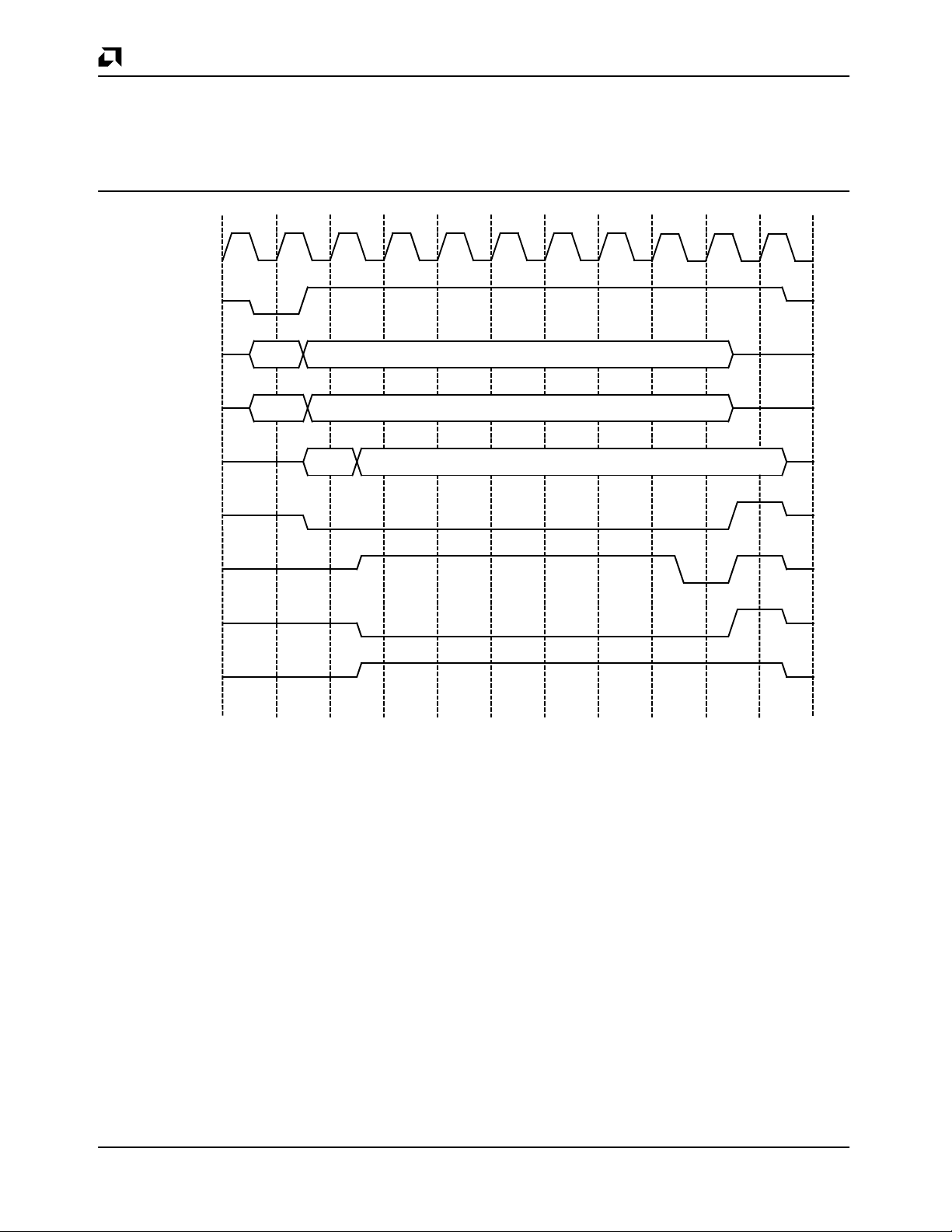
AMD
P R E L I M I N A R Y
Slave I/O Write
The Slave I/O Write command is used by the host CPU
to write to the Am79C974’s CSRs, BCRs and EEPROM
locations and SCSI and CCB registers. It is a single cycle, non-burst 8-bit, 16–bit, or 32-bit transfer which is
CLK
12345678
FRAME
AD
C/BE
PAR
IRDY
ADDR DATA
0011 BE's
PAR PAR
initiated by the host CPU. The typical number of wait
states added to a slave I/O write access on the part of
the Am79C974 controller is 6 to 7 clock cycles. The
Am79C974 controller will not produce Slave I/O write
commands while being a bus master.
91011
TRDY
DEVSEL
STOP
18681A-8
Figure 4. Slave I/O Write
30
Am79C974

P R E L I M I N A R Y
Bus Acquisition
The Am79C974 microcode (in the buffer management
section) will determine when a DMA transfer should be
initiated. The first step in any Am79C974 bus master
transfer is to acquire ownership of the bus. This task is
handled by synchronous logic within the BIU. Bus ownership is requested with the REQ signal and ownership
is granted by the arbiter through the GNT signal.
Figure 5 shows the Am79C974 controller bus acquisition. GNT is asserted at clock 3. The Am79C974 control-
ler starts driving AD[31:00] and C/BE[3:0] prior to clock
4. FRAME is asserted at clock 5 indicating a valid address and command on AD[31:00] and C/BE[3:0].
ADSTEP (bit 7) in the PCI Command register is set to
ONE to indicated that the Am79C974 controller uses address stepping. Address stepping is only used for the
first address phase of a bus master period.
CLK
FRAME
AD
C/BE
REQ
GNT
AMD
12345
ADDR
CMD
18681A-9
Figure 5. Bus Acquisition
31Am79C974

AMD
P R E L I M I N A R Y
Bus Master DMA Transfers
There are four primary types of DMA transfers. The
Am79C974 controller uses non-burst as well as burst
cycles for read and write access to the main memory.
Basic Non-Burst Read Cycles
All Am79C974 controller non-burst read accesses are of
the PCI command type Memory Read (type 6). Note that
during all non-burst read operations, the Am79C974
controller will always activate all byte enables, even
though some byte lanes may not contain valid data as
CLK
12345678
FRAME
AD
C/BE
ADDR
0110
indicated by a buffer pointer value. In such instances,
the Am79C974 controller will internally discard unneeded bytes.
Figure 6 shows a typical non-burst read access. The
Am79C974 controller asserts IRDY at clock 5 immediately after the address phase and starts sampling
DEVSEL. The target extends the cycle by asserting
DEVSEL not until clock 6. Additionally, the target inserts
one wait state by asserting its ready (TRDY) at clock 8.
9
DATA
0000
PAR
IRDY
TRDY
DEVSEL
REQ
GNT
PAR PAR
DEVSEL
is sampled by the Am79C974 controller.
Figure 6. Non-Burst Read Cycles With Wait States
18681A-10
32
Am79C974

P R E L I M I N A R Y
AMD
Figure 7 shows two non-burst read access within one arbitration cycle. The Am79C974 controller will drop
FRAME between two consecutive non-burst read cycles. The Am79C974 controller will re-request the bus
right again if it is preempted before starting the second
CLK
12345678
FRAME
AD
C/BE
PAR
IRDY
ADDR
00000110
PAR PAR
access. The example below also shows a target that can
respond to the Am79C974 controller read cycles without
wait states.
11109
DATA ADDR DATA
00000110
PAR PAR
TRDY
DEVSEL
REQ
GNT
DEVSEL
is sampled by the Am79C974 controller.
18681A-11
Figure 7. Non-Burst Read Cycles Without Wait States
33Am79C974

AMD
P R E L I M I N A R Y
Basic Non-Burst Write
All Am79C974 controller non-burst write accesses are
of the PCI command type Memory Write (type 7).
Figure 8 shows two non-burst write access within one
arbitration cycle. The Am79C974 controller will drop
FRAME between two consecutive non-burst write cycles. The Am79C974 controller will re-request the bus
CLK
12345678
FRAME
AD
C/BE
PAR
ADDR
DATA ADDR DATA
BE's0111
PAR PAR
immediately if it is preempted before starting the second
access. The example below shows an extended cycle
for the first access. The target asserts DEVSEL 2 clock
cycles after the address phase (FRAME asserted) and
adds one extra wait state by asserting TRDY only on
clock 7. The second write cycle in the example shows a
ZERO wait state access.
9
10 11
BE's0111
PAR PAR
IRDY
TRDY
DEVSEL
REQ
GNT
DEVSEL
is sampled by the Am79C974 controller.
Figure 8. Non-Burst Write Cycles With and Without Wait States
18681A-12
34
Am79C974

P R E L I M I N A R Y
AMD
Basic Burst Read Cycles
All Am79C974 controller burst read transfers are of the
PCI command type Memory Read Line (type14).
AD[1:0] will both be ZERO during the address phase indicating a linear burst order. All four byte enable signals
will be ZERO during the data phase as the Am79C974
controller always reads a full 32-bit word when in burst
CLK
12345678
FRAME
AD
C/BE
PAR
ADDR
PAR
DATA DATA DATA DATA
00001110
mode.
Figure 9 shows a typical burst read access. The
Am79C974 controller arbitrates for the bus, is granted
access, and reads four 32-bit words (DWORD) from
system memory and then releases the bus. All four data
phases in this example take two clock cycles each,
which is determined by the timing of TRDY.
11109 12
PAR PAR PAR PAR
13
IRDY
TRDY
DEVSEL
REQ
GNT
DEVSEL
is sampled by the Am79C974 controller.
18681A-13
Figure 9. Burst Read Cycles
35Am79C974

AMD
P R E L I M I N A R Y
Basic Burst Write Cycles
All Am79C974 controller burst write transfers are of the
PCI command type Memory Write (type 7). AD[1:0] will
both be ZERO during the address phase indicating a linear burst order. All four byte enable signals will be ZERO
during the data phase as the Am79C974 controller always writes a full 32-bit word when in burst mode.
Figure 10 shows a typical burst write access. The
CLK
12345678
FRAME
AD
C/BE
PAR
ADDR DATA DATA DATA
Am79C974 controller arbitrates for the bus, is granted
access, and writes four 32-bit words (DWORDs) from
system memory and then releases the bus. In this example, the memory system extends the data phase of
the first access by one wait state. The following three
data phases take one clock cycle each, which is determined by the timing of TRDY.
109
DATA
00000111
PAR PAR PAR PAR
PAR
IRDY
TRDY
DEVSEL
REQ
GNT
DEVSEL
is sampled by the Am79C974 controller.
18681A-14
Figure 10. Burst Write Cycles
36
Am79C974

P R E L I M I N A R Y
AMD
Transaction Termination
Termination of a PCI transaction may be initiated by
either the master or the target. During termination, the
master remains in control to bring all PCI transactions to
an orderly and systematic conclusion regardless of what
caused the termination. All transactions are concluded
when FRAME and IRDY are both deasserted, indicating
an IDLE cycle.
Target Initiated Termination
When the Am79C974 controller is a bus master, the cycles it produces on the PCI bus may be terminated by
the target in one of three different ways: Disconnect with
data transfer, disconnect without data transfer, and target abort.
CLK
12345678
FRAME
AD
ADDR
DATA DATA
i
Disconnect With Data Transfer
Figure 11 shows a disconnection in which one last data
transfer occurs after the target asserted STOP. STOP is
asserted on clock 4 to start the termination sequence.
Data is still transferred during this cycles, since both
IRDY and TRDY are asserted. The Am79C974 control-
ler terminates the current transfer with the deassertion
of FRAME on clock 5 and then one clock cycle later with
the deassertion of IRDY. It finally releases the bus on
clock 6. The Am79C974 controller will re-request the
bus after 2 clock cycles, if it wants to transfer more data.
The starting address of the new transfer will be the address of the next untransferred data.
109
11
ADDR +8
i
C/BE
PAR
IRDY
TRDY
DEVSEL
STOP
REQ
GNT
DEVSEL
00000111
PAR PAR PAR
is sampled by the Am79C974 controller.
0111
18681A-15
Figure 11. Disconnect with Data Transfer
37Am79C974

AMD
P R E L I M I N A R Y
Disconnect Without Data Transfer
Figure 12 shows a target disconnect sequence during
which no data is transferred. STOP is asserted on clock
4 without TRDY being asserted at the same time. The
Am79C974 controller terminates the current transfer
with the deassertion of FRAME on clock 5 and one clock
CLK
12345678
FRAME
AD
C/BE
PAR
IRDY
ADDRi ADDRi
DATA
00000111
PAR PAR
cycle later with the deassertion of IRDY. It finally releases the bus on clock 6. The Am79C974 controller will
re-request the bus after 2 clock cycles to retry the last
transfer. The starting address of the new transfer will be
the same address as of the last untransferred data.
109
11
0111
TRDY
DEVSEL
STOP
REQ
GNT
DEVSEL
is sampled by the Am79C974 controller.
18681A-16
Figure 12. Disconnect Without Data Transfer
38
Am79C974

P R E L I M I N A R Y
AMD
Target Abort
Figure 13 shows a target abort sequence. The target asserts DEVSEL for one clock. It then deasserts DEVSEL
and asserts STOP on clock 4. A target can use the target
abort sequence to indicate that it cannot service the data
transfer and that it does not want the transaction to be
retried. Additionally, the Am79C974 controller cannot
make any assumption about the success of the previous
data transfers in the current transaction. The
Am79C974 controller terminates the current transfer
with the deassertion of FRAME on clock 5 and one clock
cycle later with the deassertion of IRDY. It finally releases the bus on clock 6.
CLK
123456
FRAME
AD
C/BE
ADDR
DATA
Since data integrity is not guaranteed, the Am79C974
controller cannot recover from a target abort event. For
Ethernet, the Am79C974 controller will reset all CSR
and BCR locations to their H_RESET values. Any ongoing network activity will be stopped immediately. The
PCI configuration registers will not be cleared. For
SCSI, when target aborts, INTA will not be asserted, but
the ABORT bit (bit 2 of the DMA status register at offset
54h), is set. For either Ethernet or SCSI a target abort
causes RTABORT (bit 12) of the status register in the
appropriate PCI configuration space to beset.
00000111
PAR
IRDY
TRDY
DEVSEL
STOP
REQ
GNT
DEVSEL
PAR PAR
is sampled by the Am79C974 controller.
18681A-17
Figure 13. Target Abort
39Am79C974

AMD
P R E L I M I N A R Y
Master Initiated Termination
There are three scenarios besides normal completion of
a transaction where the Am79C974 controller will terminate the cycles it produces on the PCI bus. These are
Preemption with and without FRAME assertion and
Master Abort.
Preemption When FRAME is Deasserted
The Am79C974 controller can generate multiple address phases during a single bus ownership period
CLK
12345678
FRAME
AD
C/BE
PAR
ADDR
when transferring data. FRAME is deasserted in between two address phases. While FRAME is deasserted, the central arbiter can remove GNT to the
Am79C974 controller at any time to service another
master. When GNT is removed, the Am79C974 controller will finish the current transfer and then release the
bus. It will keep REQ asserted to regain bus ownership
as soon as possible.
DATA
BE's0111
PAR PAR
IRDY
TRDY
DEVSEL
REQ
GNT
DEVSEL
is sampled by the Am79C974 controller.
Figure 14. Preemption When FRAME is Deasserted
18681A-18
40
Am79C974

P R E L I M I N A R Y
AMD
Preemption When FRAME is Asserted
The central arbiter can take GNT to the Am79C974 controller away if the current bus operation takes too long.
This may happen, for example, when the Am79C974
controller tries to fill the whole Ethernet transmit FIFO
and the target inserts extra wait states for every data
phase. When GNT is taken away, the Am79C974 con-
CLK
12345678
FRAME
AD
C/BE
PAR
IRDY
ADDR DATA DAT A DATA
troller will finish the current transfer and then immediately release the bus. The Latency Timer in PCI
configuration space of the Am79C974 controller is always set to ZERO. The Am79C974 controller will keep
REQ asserted to regain bus ownership as soon as possible.
9
00000111
PAR PAR PAR PAR
TRDY
DEVSEL
REQ
GNT
DEVSEL
is sampled by the Am79C974 controller.
Figure 15. Preemption When FRAME is Asserted
18681A-19
41Am79C974

AMD
P R E L I M I N A R Y
Master Abort
The Am79C974 controller will terminate its cycle with a
Master Abort sequence if DEVSEL is not asserted within
4 clocks after FRAME is asserted. Master Abort is
treated as a fatal error by the Am79C974 controller. For
the Ethernet, the Am79C974 controller will reset all CSR
and BCR locations to their H_RESET values. Any
on-going network activity will be stopped immediately.
CLK
12345678
FRAME
AD
C/BE
PAR
ADDR DATA
The PCI configuration registers will not be cleared. For
SCSI, when the master aborts, INTA will not be asserted, but the ABORT bit (bit 2 of the DMA status register at offset 54h), is set. For either Ethernet or SCSI
master abort causes RMABORT (bit 13) of the status
register in the appropriate PCI configuration space to
beset.
109
00000111
PAR PAR
IRDY
TRDY
DEVSEL
REQ
GNT
DEVSEL
is sampled by the Am79C974 controller.
18681A-20
Figure 16. Master Abort
42
Am79C974

P R E L I M I N A R Y
AMD
Ethernet Controller
Buffer Management Unit (BMU)
The buffer management unit is a micro-coded state machine which implements the initialization procedure and
manages the descriptors and buffers. The buffer management unit operates at half the speed of the
CLKinput.
Initialization
Am79C974 initialization includes the reading of the initialization block in memory to obtain the operating parameters. The initialization block is read when the INIT
bit in CSR0 is set. The INIT bit should be set before or
concurrent with the STRT bit to insure correct operation.
Two DWORDs are read during each period of bus mastership. When SSIZE32 = 1 (BCR20, bit 8), this results
in a total of 4 arbitration cycles (3 arbitration cycles if
SSIZE32 = 0). Once the initialization block has been
completely read in and internal registers have been updated, IDON will be set in CSR0, and an interrupt generated (if IENA is set). At this point, the BMU knows where
the receive and transmit descriptor rings and hence,
normal network operations will begin.
The Am79C974 controller obtains the start address of
the Initialization Block from the contents of CSR1 (least
significant 16 bits of address) and CSR2 (most significant 16 bits of address). The host must write CSR1 and
CSR2 before setting the INIT bit. The block contains the
user defined conditions for Am79C974 operation, together with the base addresses and length information
of the transmit and receive descriptor rings.
There is an alternative method to initialize the
Am79C974 controller. Instead of initialization via the initialization block in memory, data can be written directly
into the appropriate registers. Either method may be
used at the discretion of the programmer. If the registers
are written to directly, the INIT bit must not be set, or the
initialization block will be read in, thus overwriting the
previously written information. Please refer to Appendix
C for details on this alternative method.
If initialization is done by writing directly to registers, the
Polling Interval register (CSR47) must be initialized in
addition to those registers that can be loaded automatically from the initialization block.
Re-Initialization
The transmitter and receiver sections of the Am79C974
controller can be turned on via the initialization block
(MODE Register DTX, DRX bits; CSR15[1:0]). The
states of the transmitter and receiver are monitored by
the host through CSR0 (RXON, TXON bits). The
Am79C974 controller should be reinitialized if the transmitter and/or the receiver were not turned on during the
original initialization, and it was subsequently required
to activate them or if either section was shut off due to
the detection of certain error conditions (MERR, UFLO,
TX BUFFerror).
Reinitialization may be done via the initialization block or
by setting the STOP bit in CSR0, followed by writing to
CSR15, and then setting the START bit in CSR0. Note
that this form of restart will not perform the same in the
Am79C974 controller as in the LANCE. In particular,
upon restart, the Am79C974 controller reloads the
transmit and receive descriptor pointers with their respective base addresses. This means that the software
must clear the descriptor own bits and reset its descriptor ring pointers before the restart of the Am79C974
controller. The reload of descriptor base addresses is
performed in the LANCE only after initialization, so a restart of the LANCE without initialization leaves the
LANCE pointing at the same descriptor locations as before the restart.
Buffer Management
Buffer management is accomplished through message
descriptor entries organized as ring structures in memory. There are two rings, a receive ring and a transmit
ring. The size of a message descriptor entry is 4
DWORDs, or 16 bytes, when SSIZE32 = 1. The size of a
message descriptor entry is 4 words, or 8 bytes, when
SSIZE32 = 0.
Descriptor Rings
Each descriptor ring must be organized in a contiguous
area of memory. At initialization time (setting the INIT bit
in CSR0), the Am79C974 controller reads the user-defined base address for the transmit and receive descriptor rings, as well as the number of entries contained in
the descriptor rings. Descriptor ring base addresses
must be on a 16-byte boundary when SSIZE32=1, and
8-byte boundary when SSIZE=0. A maximum of 128 (or
512, depending upon the value of SSIZE32) ring entries
is allowed when the ring length is set through the TLEN
and RLEN fields of the initialization block. However, the
ring lengths can be set beyond this range (up to 65535)
by writing the transmit and receive ring length registers
(CSR76, CSR78) directly.
Each ring entry contains the following information:
1. The address of the actual message data buffer in
user or host memory
2. The length of the message buffer
3. Status information indicating the condition of the
buffer
To permit the queuing and de-queuing of message buffers, ownership of each buffer is allocated to either the
Am79C974 controller or the host. The OWN bit within
the descriptor status information, either TMD or RMD
(see section on TMD or RMD), is used for this purpose.
OWN= “1” signifies that the Am79C974 controller cur-
43Am79C974

AMD
P R E L I M I N A R Y
rently has ownership of this ring descriptor and its
associated buffer. Only the owner is permitted to relinquish ownership or to write to any field in the descriptor
entry. A device that is not the current owner of a descriptor entry cannot assume ownership or change any field
in the entry. A device may, however, read from a descriptor that it does not currently own. Software should
always read descriptor entries in sequential order.
When software finds that the current descriptor is owned
by the Am79C974 controller, then the software must not
read “ahead” to the next descriptor. The software should
wait at the unOWNed descriptor until ownership has
been granted to the software (when LAPPEN = 1
(CSR3, bit 5), then this rule is modified. See the LAPPEN description). Strict adherence to these rules insures that “Deadly Embrace” conditions are avoided.
Descriptor Ring Access Mechanism
At initialization, the Am79C974 controller reads the
24-Bit Base Address
Pointer to
Initialization Block
RES
CSR2
IADR[23:16]
CSR1
IADR[15:0]
base address of both the transmit and receive descriptor
rings into CSRs for use by the Am79C974 controller during subsequent operations.
As the final step in the self-initialization process, the
base address of each ring is loaded into each of the current descriptor address registers and the address of the
next descriptor entry in the transmit and receive rings is
computed and loaded into each of the next descriptor
address registers.
When SSIZE32 = 0, software data structures are 16 bits
wide. The following diagram, Figure 17, illustrates the
relationship between the Initialization Base Address,
the Initialization Block, the Receive and Transmit Descriptor Ring Base Addresses, the Receive and Transmit Descriptors and the Receive and Transmit Data
Buffers, for the case of SSIZE32 = 0.
N
N
N
N
•
•
•
Rcv Descriptor
Ring
1st desc.
start
2nd desc.
start
Initialization
Block
MODE
PADR[15:0]
PADR[31:16]
PADR[47:32]
LADRF[15:0]
LADRF[31:16]
LADRF[47:32]
LADRF[63:48]
RDRA[15:0]
RLEN RES RDRA[23:16]
TDRA[15:0]
TLEN RES TDRA[23:16]
Rcv
Buffers
Xmt
Buffers
RMD0
RMD1
Data
Buffer
1
M
RX DESCRIPTOR RINGS
Xmt Descriptor
RX DESCRIPTOR RINGS
1st desc.
start
TMD0
TMD1
Data
Buffer
1
RMD2
Data
Buffer
Ring
TMD2
Data
Buffer
M
TMD3
•
RMD0
•••
M
2nd desc.
start
TMD0
•
•
Data
Buffer
N
•
Data
Buffer
M
•
•
RMD3
2
M
2
44
Figure 17. 16-Bit Data Structures: Initialization Block and Descriptor Rings
Am79C974
18681A-21

P R E L I M I N A R Y
AMD
When SSIZE32 = 1, software data structures are 32 bits
wide. The following diagram illustrates, Figure 18, the
relationship between the Initialization Base Address,
the Initialization Block, the Receive and Transmit
32-Bit Base Address
Pointer to
Initialization Block
CSR2
IADR[31:16] IADR[15:0]
CSR1
Initialization
Block
TLEN
RES
RLEN
RES
PADR[31:0]
RES
LADRF[31:0]
LADRF[63:32]
RDRA[31:0]
TDRA[31:0]
MODE
PADR[47:32]
Descriptor Ring Base Addresses, the Receive and
Transmit Descriptors and the Receive and Transmit
Data Buffers, for the case of SSIZE32 = 1.
N
N
N
N
•
•
•
Rcv Descriptor
Ring
Rcv
Buffers
1st desc.
start
RMD0
RMD1
Data
Buffer
1
M
RX DESCRIPTOR RINGS
RMD2
Data
Buffer
2
M
RMD3
2nd desc.
start
RMD0
•
•
M
Data
•
Buffer
N
M
•
•
•
Xmt Descriptor
Xmt
Buffers
RX DESCRIPTOR RINGS
1st desc.
start
TMD0
Data
Buffer
1
TMD1
Ring
TMD2
Data
Buffer
2nd desc.
start
TMD0
TMD3
•
•
•
2
Figure 18. 32-Bit Data Structures: Initialization Block and Descriptor Rings
Data
Buffer
M
18681A-22
45Am79C974

AMD
P R E L I M I N A R Y
Polling
If there is no network channel activity and there is no
pre- or post-receive or pre- or post-transmit activity being performed by the Am79C974 controller, then the
Am79C974 controller will periodically poll the current receive and transmit descriptor entries in order to ascertain their ownership. If the DPOLL bit in CSR4 is set,
then the transmit polling function is disabled.
A typical polling operation consists of the following: The
Am79C974 controller will use the current receive descriptor address stored internally to vector to the appropriate Receive Descriptor Table Entry (RDTE). It will
then use the current transmit descriptor address (stored
internally) to vector to the appropriate Transmit Descriptor Table Entry (TDTE). The accesses will be made in
the following order: RMD1, then RMD0 of the current
RDTE during one bus arbitration, and after that, TMD1,
then TMD0 of the current TDTE during a second bus arbitration. All information collected during polling activity
will be stored internally in the appropriate CSRs. (i.e.
CSR18, CSR19, CSR20, CSR21, CSR40, CSR42,
CSR50, CSR52). UnOWNed descriptor status will be internally ignored.
A typical receive poll is the product of the following
conditions:
1. Am79C974 controller does not possess ownership
of the current RDTE and the poll time has elapsed
and RXON=1 (CSR0, bit 5), or
2. Am79C974 controller does not possess ownership
of the next RDTE the poll time has elapsed and
RXON=1.
If RXON=0 the Am79C974 controller will never poll
RDTE locations.
The ideal system should always have at least one RDTE
available for the possibility of an unpredictable receive
event. (This condition is not a requirement. If this condition is not met, it simply means that frames will be
missed by the system because there was no buffer
space available.) But the typical system usually has at
least one or two RDTEs available for the possibility of an
unpredictable receive event. Given that this condition is
satisfied, the current and next RDTE polls are rarely
seen and hence, the typical poll operation simply consists of a check of the status of the current TDTE. When
there is only one RDTE (because the RLEN was set to
ZERO), then there is no “next RDTE” and ownership of
“next RDTE” cannot be checked. If there is at least one
RDTE, the RDTE poll will rarely be seen and the typical
poll operation simply consists of a check of the
currentTDTE.
A typical transmit poll is the product of the following
conditions:
1. Am79C974 controller does not possess ownership
of the current TDTE and
46
Am79C974
DPOLL=0 (CSR4, bit 2) and
TXON=1 (CSR0, bit 4) and
the poll time has elapsed, or
2. Am79C974 controller does not possess ownership
of the current TDTE and
DPOLL=0 and
TXON=1 and
a frame has just been received, or
3. Am79C974 controller does not possess ownership
of the current TDTE and
DPOLL=0 and
TXON=1 and
a frame has just been transmitted.
Setting the TDMD bit of CSR0 will cause the microcode
controller to exit the poll counting code and immediately
perform a polling operation. If RDTE ownership has not
been previously established, then an RDTE poll will be
performed ahead of the TDTE poll. If the microcode is
not executing the poll counting code when the TDMD bit
is set, then the demanded poll of the TDTE will be delayed until the microcode returns to the poll
countingcode.
The user may change the poll time value from the default of 65,536 clock periods by modifying the value in
the Polling Interval register (CSR47). Note that if a non–
default value is desired, then a strict sequence of setting
the INIT bit in CSR0, waiting for the IDON bit in CSR0,
then writing to CSR47, and then setting STRT in CSR0
must be observed, otherwise the default value will not
be overwritten. See the CSR47 section for details.
Transmit Descriptor Table Entry (TDTE)
If, after a TDTE access, the Am79C974 controller finds
that the OWN bit of that TDTE is not set, then the
Am79C974 controller resumes the poll time count and
reexamines the same TDTE at the next expiration of the
poll time count.
If the OWN bit of the TDTE is set, but Start of Frame
(STP) bit is not set, the Am79C974 controller will immediately request the bus in order to reset the OWN bit of
this descriptor. (This condition would normally be found
following a LCOL or RETRY error that occurred in the
middle of a transmit frame chain of buffers.) After resetting the OWN bit of this descriptor, the Am79C974 controller will again immediately request the bus in order to
access the next TDTE location in the ring.
If the OWN bit is set and the buffer length is 0, the OWN
bit will be reset. In the LANCE the buffer length of 0 is
interpreted as a 4096-byte buffer. It is acceptable to
have a 0 length buffer on transmit with STP = 1 or
and
STP=1
length buffer with STP = 0 and ENP =1.
If the OWN bit is set and the start of frame (STP) bit is
set, then microcode control proceeds to a routine that
will enable transmit data transfers to the FIFO. The
ENP = 1. It is not acceptable to have 0

P R E L I M I N A R Y
AMD
Am79C974 controller will look ahead to the next transmit descriptor after it has performed at least one transmit data transfer from the first buffer. (More than one
transmit data transfer may possibly take place, depending upon the state of the transmitter.) The contents of
TMD0 and TMD1 will be stored in Next Xmt Buffer Address (CSR64 and CSR65), Next Xmt Byte Count
(CSR66) and Next Xmt Status (CSR67) regardless of
the state of the OWN bit. This transmit descriptor
lookahead operation is performed only once.
If the Am79C974 controller does not own the next TDTE
(i.e. the second TDTE for this frame), then it will complete transmission of the current buffer and then update
the status of the current (first) TDTE with the BUFF and
UFLO bits being set. This will cause the transmitter to be
disabled (CSR0, TXON=0). The Am79C974 controller
will have to be re-initialized to restore the transmit function. The situation that matches this description implies
that the system has not been able to stay ahead of the
Am79C974 controller in the transmit descriptor ring and
therefore, the condition is treated as a fatal error. (To
avoid this situation, the system should always set the
transmit chain descriptor own bits in reverse order.)
If the Am79C974 controller does own the second TDTE
in a chain, it will gradually empty the contents of the first
buffer (as the bytes are needed by the transmit operation), perform a single-cycle DMA transfer to update the
status of the first descriptor (reset the OWN bit in
TMD1), and then it may perform one data DMA access
on the second buffer in the chain before executing another lookahead operation. (i.e. a lookahead to the third
descriptor.)
The Am79C974 controller can queue up to two frames in
the transmit FIFO. Call them frame “X” and frame “Y”,
where “Y” is after “X”. Assume that frame “X” is currently
being transmitted. Because the Am79C974 controller
can perform lookahead data transfer past the ENP of
frame “X”, it is possible for the Am79C974 controller to
completely transfer the data from a buffer belonging to
frame “Y” into the FIFO even though frame “X” has not
yet been completely transmitted. At the end of this “Y”
buffer data transfer, the Am79C974 controller will write
intermediate status (change the OWN bit to a ZERO) for
the “Y” frame buffer, if frame “Y” uses data chaining.
The last TDTE for the “X” frame (containing ENP) has
not yet been written, since the “X” frame has not yet
been completely transmitted. Note that the Am79C974
controller has, in this instance, returned ownership of a
TDTE to the host out of a “normal” sequence.
For this reason, it becomes imperative that the host system should never read the Transmit DTE ownership bits
out of order. Software should always process buffers in
sequence, waiting for the ownership before proceeding.
There should be no problems for software which processes buffers in sequence, waiting for ownership before
proceeding.
If an error occurs in the transmission before all of the
bytes of the current buffer have been transferred, then
TMD2 and TMD1 of the current buffer will be written; In
such a case, data transfers from the next buffer will not
commence. Instead, following the TMD2/TMD1 update,
the Am79C974 controller will go to the next transmit
frame, if any, skipping over the rest of the frame which
experienced an error, including chained buffers. This is
done by returning to the polling microcode where
Am79C974 controller will immediately access the next
descriptor and find the condition OWN=1 and STP=0 as
described earlier. As described for that case, the
Am79C974 controller will reset the own bit for this descriptor and continue in like manner until a descriptor
with OWN=0 (no more transmit frames in the ring) or
OWN=1 and STP=1 (the first buffer of a new frame)
is reached.
At the end of any transmit operation, whether successful
or with errors, immediately following the completion of
the descriptor updates, the Am79C974 controller will always perform another poll operation. As described earlier, this poll operation will begin with a check of the
current RDTE, unless the Am79C974 controller already
owns that descriptor. Then the Am79C974 controller will
proceed to polling the next TDTE. If the transmit descriptor OWN bit has a ZERO value, then the Am79C974
controller will resume poll time count incrementing. If the
transmit descriptor OWN bit has a value of ONE, then
the Am79C974 controller will begin filling the FIFO with
transmit data and initiate a transmission. This end–of–
operation poll coupled with the TDTE lookahead operation allows the Am79C974 controller to avoid inserting
poll time counts between successive transmit frames.
Whenever the Am79C974 controller completes a transmit frame (either with or without error) and writes the
status information to the current descriptor, then the
TINT bit of CSR0 is set to indicate the completion of a
transmission. This causes an interrupt signal if the IENA
bit of CSR0 has been set and the TINTM bit of CSR3
isreset.
47Am79C974

AMD
P R E L I M I N A R Y
Receive Descriptor Table Entry (RDTE)
If the Am79C974 controller does not own both the current and the next Receive Descriptor Table Entry then
the Am79C974 controller will continue to poll according
to the polling sequence described above. If the receive
descriptor ring length is 1, then there is no next descriptor to be polled.
If a poll operation has revealed that the current and the
next RDTE belong to the Am79C974 controller then additional poll accesses are not necessary. Future poll operations will not include RDTE accesses as long as the
Am79C974 controller retains ownership of the current
and the next RDTE.
When receive activity is present on the channel, the
Am79C974 controller waits for the complete address of
the message to arrive. It then decides whether to accept
or reject the frame based on all active addressing
schemes. If the frame is accepted the Am79C974 controller checks the current receive buffer status register
CRST (CSR41) to determine the ownership of the current buffer.
If ownership is lacking, then the Am79C974 controller
will immediately perform a (last ditch) poll of the current
RDTE. If ownership is still denied, then the Am79C974
controller has no buffer in which to store the incoming
message. The Missed Frame Count register (CSR112)
will be incremented and the MISS bit will be set in CSR0
and an interrupt will be generated if IENA=1 (CSR0) and
MISSM=0 (CSR3). Another poll of the current RDTE will
not occur until the frame has finished.
If the Am79C974 controller sees that the last poll (either
a normal poll, or the last-ditch effort described in the
above paragraph) of the current RDTE shows valid ownership, then it proceeds to a poll of the next RDTE. Following this poll, and regardless of the outcome of this
poll, transfers of receive data from the FIFO may begin.
Regardless of ownership of the second receive descriptor, the Am79C974 controller will continue to perform receive data DMA transfers to the first buffer. If the frame
length exceeds the length of the first buffer, and the
Am79C974 controller does not own the second buffer,
ownership of the current descriptor will be passed back
to the system by writing a ZERO to the OWN bit of
RMD1 and status will be written indicating buffer
(BUFF=1) and possibly overflow (OFLO=1) errors.
If the frame length exceeds the length of the first (current) buffer, and the Am79C974 controller does own the
second (next) buffer, ownership will be passed back to
the system by writing a ZERO to the OWN bit of RMD1
when the first buffer is full. Receive data transfers to the
second buffer may occur before the Am79C974 controller proceeds to look ahead to the ownership of the third
buffer. Such action will depend upon the state of the
FIFO when the status has been updated on the first de-
48
Am79C974
scriptor. In any case, lookahead will be performed to the
third buffer and the information gathered will be stored in
the chip, regardless of the state of the ownership bit. As
in the transmit flow, lookahead operations are performed only once.
This activity continues until the Am79C974 controller
recognizes the completion of the frame (the last byte of
this receive message has been removed from the
FIFO). The Am79C974 controller will subsequently update the current RDTE status with the end of frame
(ENP) indication set, write the message byte count
(MCNT) of the complete frame into RMD2 and overwrite
the “current” entries in the CSRs with the “next” entries.
Media Access Control
The Media Access Control engine incorporates the essential protocol requirements for operation of a compliant Ethernet/802.3 node, and provides the interface
between the FIFO sub-system and the Manchester Encoder/Decoder (MENDEC).
The MAC engine is fully compliant to Section 4 of ISO/
IEC 8802-3 (ANSI/IEEE Standard 1990 Second edition)
and ANSI/IEEE 802.3 (1985).
The MAC engine provides programmable enhanced
features designed to minimize host supervision, bus
utilization, and pre- or post- message processing.
These include the ability to disable retries after a collision, dynamic FCS generation on a frame-by-frame basis, and automatic pad field insertion and deletion to
enforce minimum frame size attributes, automatic
retransmission without reloading the FIFO, automatic
deletion of collision fragments, and reduces bus
bandwidth use.
The two primary attributes of the MAC engine are:
Transmit and receive message data encapsulation.
— Framing (frame boundary delimitation, frame
synchronization).
— Addressing (source and destination address
handling).
— Error detection (physical medium transmission
errors).
Media access management.
— Medium allocation (collision avoidance).
— Contention resolution (collision handling).
Transmit and Receive Message Data
Encapsulation
The MAC engine provides minimum frame size enforcement for transmit and receive frames. When
APAD_XMT = 1 (CSR, bit 11), transmit messages will
be padded with sufficient bytes (containing 00h) to ensure that the receiving station will observe an information field (destination address, source address,
length/type, data and FCS) of 64-bytes. When

P R E L I M I N A R Y
AMD
ASTRP_RCV = 1 (CSR4, bit 10), the receiver will
automatically strip pad bytes from the received message by observing the value in the length field, and stripping excess bytes if this value is below the minimum
data size (46 bytes). Both features can be independently over-ridden to allow illegally short (less than 64
bytes of frame data) messages to be transmitted and/or
received. The use of this feature reduces bus utilization
because the pad bytes are not transferred into or out of
main memory.
Framing (Frame Boundary Delimitation, Frame
Synchronization)
The MAC engine will autonomously handle the construction of the transmit frame. Once the Transmit FIFO
has been filled to the predetermined threshold (set by
XMTSP in CSR80), and providing access to the channel
is currently permitted, the MAC engine will commence
the 7 byte preamble sequence (10101010b, where first
bit transmitted is a 1). The MAC engine will subsequently append the Start Frame Delimiter (SFD) byte
(10101011b) followed by the serialized data from the
Transmit FIFO. Once the data has been completed, the
MAC engine will append the FCS (most significant bit
first) which was computed on the entire data portion of
the frame. The data portion of the frame consists of destination address, source address, length/type, and
frame data.
The user is responsible for the correct ordering and content in each of the fields in the frame.
The receive section of the MAC engine will detect an incoming preamble sequence and lock to the encoded
clock. The internal MENDEC will decode the serial bit
stream and present this to the MAC engine. The MAC
will discard the first 8-bits of information before searching for the SFD sequence. Once the SFD is detected, all
subsequent bits are treated as part of the frame. The
MAC engine will inspect the length field to ensure minimum frame size, strip unnecessary pad characters (if
enabled), and pass the remaining bytes through the Receive FIFO to the host. If pad stripping is performed, the
MAC engine will also strip the received FCS bytes, although the normal FCS computation and checking will
occur. Note that apart from pad stripping, the frame will
be passed unmodified to the host. If the length field has
a value of 46 or greater, the MAC engine will not attempt
to validate the length against the number of bytes contained in the message.
If the frame terminates or suffers a collision before
64-bytes of information (after SFD) have been received,
the MAC engine will automatically delete the frame from
the Receive FIFO, without host intervention. The
Am79C974 controller has the ability to accept runt packets for diagnostics purposes and proprietary networks.
Addressing (Source and Destination Address
Handling)
The first 6-bytes of information after SFD will be interpreted as the destination address field. The MAC engine
provides facilities for physical, logical (multicast) and
broadcast address reception.
Error Detection (Physical Medium Transmission
Errors)
The MAC engine provides several facilities which report
and recover from errors on the medium. In addition, the
network is protected from gross errors due to inability of
the host to keep pace with the MAC engine activity.
On completion of transmission, the following transmit
status is available in the appropriate TMD and CSR
areas:
The exact number of transmission retry attempts
(ONE, MORE, RTRY or TRC).
Whether the MAC engine had to Defer (DEF) due
to channel activity.
Excessive deferral (EXDEF), indicating that the
transmitter has experienced Excessive Deferral on
this transmit frame, where Excessive Deferral is
defined in ISO 8802-3 (IEEE/ANSI 802.3).
Loss of Carrier (LCAR), indicating that there was
an interruption in the ability of the MAC engine to
monitor its own transmission. Repeated
LCAR errors indicate a potentially faulty transceiver or network connection.
Late Collision (LCOL) indicates that the transmission suffered a collision after the slot time. This is
indicative of a badly configured network. Late collisions should not occur in a normal operating network.
Collision Error (CERR) indicates that the transceiver did not respond with an SQE Test message
within the predetermined time after a transmission
completed. This may be due to a failed transceiver,
disconnected or faulty transceiver drop cable, or
the fact the transceiver does not support this feature (or it is disabled).
In addition to the reporting of network errors, the MAC
engine will also attempt to prevent the creation of any
network error due to the inability of the host to service
the MAC engine. During transmission, if the host fails to
keep the Transmit FIFO filled sufficiently, causing an underflow, the MAC engine will guarantee the message is
either sent as a runt packet (which will be deleted by the
receiving station) or has an invalid FCS (which will also
cause the receiver to reject the message).
49Am79C974

AMD
P R E L I M I N A R Y
The status of each receive message is available in the
appropriate RMD and CSR areas. FCS and Framing errors (FRAM) are reported, although the received frame
is still passed to the host. The FRAM error will only be
reported if an FCS error is detected and there are a non
integral number of bytes in the message. The MAC engine will ignore up to 7 additional bits at the end of a message (dribbling bits), which can occur under normal
network operating conditions. The reception of 8 additional bits will cause the MAC engine to de-serialize the
entire byte, and will result in the received message and
FCS being modified.
The Am79C974 controller can handle up to 7 dribbling
bits when a received frame terminates. During the reception, the FCS is generated on every serial bit (including the dribbling bits) coming from the cable, although
the internally saved FCS value is only updated on the
eighth bit (on each byte boundary). The framing error is
reported to the user as follows:
If the number of dribbling bits are 1 to 7 and there
is no CRC (FCS) error, then there is no Framing
error (FRAM = 0).
If the number of dribbling bits are 1 to 7 and there
is a CRC (FCS) error, then there is also a Framing
error (FRAM = 1).
If the number of dribbling bits = 0, then there is no
Framing error. There may or may not be a CRC
(FCS) error.
Counters are provided to report the Receive Collision
Count and Runt Packet Count for network statistics and
utilization calculations.
Note that if the MAC engine detects a received frame
which has a 00b pattern in the preamble (after the first 8
bits which are ignored), the entire frame will be ignored.
The MAC engine will wait for the network to go inactive
before attempting to receive additional frames.
Media Access Management
The basic requirement for all stations on the network is
to provide fairness of channel allocation. The
802.3/Ethernet protocols define a media access mechanism which permits all stations to access the channel
with equality. Any node can attempt to contend for the
channel by waiting for a predetermined time (Inter Packet Gap internal) after the last activity, before transmitting
on the media. The channel is a multidrop communications media (with various topological configurations permitted) which allows a single station to transmit and all
other stations to receive. If two nodes simultaneously
contend for the channel, their signals will interact causing loss of data, defined as a collision. It is the responsibility of the MAC to attempt to avoid and recover from a
collision, to guarantee data integrity for the end-to-end
transmission to the receiving station.
50
Am79C974
Medium Allocation
The IEEE/ANSI 802.3 Standard (ISO/IEC 8802-3 1990)
requires that the CSMA/CD MAC monitor the medium
for traffic by watching for carrier activity. When carrier is
detected, the media is considered busy, and the MAC
should defer to the existing message.
The ISO 8802-3 (IEEE/ANSI 802.3) Standard also allows optional two part deferral after a receive message.
See ANSI/IEEE Std 802.3 –1990 Edition, 4.2.3.2.1:
Note: It is possible for the PLS carrier sense indication
to fail to be asserted during a collision on the media. If
the deference process simply times the interFrame gap
based on this indication it is possible for a short interFrame gap to be generated, leading to a potential reception failure of a subsequent frame. To enhance system
robustness the following optional measures, as specified in 4.2.8, are recommended when InterFrameSpacingPart1 is other than ZERO:
1. Upon completing a transmission, start timing the
interpacket gap, as soon as transmitting and carrier Sense are both false.
2. When timing an interFrame gap following reception, reset the interFrame gap timing if carrier
Sense becomes true during the first 2/3 of the interFrame gap timing interval. During the final 1/3 of
the interval the timer shall not be reset to ensure
fair access to the medium. An initial period shorter
than 2/3 of the interval is permissible including
ZERO.
The MAC engine implements the optional receive two
part deferral algorithm, with a first part inter-frame-spacing time of 6.0 µs. The second part of the inter-framespacing interval is therefore 3.6 µs.
The Am79C974 controller will perform the two part deferral algorithm as specified in Section 4.2.8 (Process
Deference). The Inter Packet Gap (IPG) timer will start
timing the 9.6 µs InterFrameSpacing after the receive
carrier is de-asserted. During the first part deferral (InterFrameSpacingPart1 – IFS1) the Am79C974 controller will defer any pending transmit frame and respond to
the receive message. The IPG counter will be reset to
ZERO continuously until the carrier de-asserts, at which
point the IPG counter will resume the 9.6 µs count once
again. Once the IFS1 period of 6.0 µs has elapsed, the
Am79C974 controller will begin timing the second part
deferral (InterFrame Spacing Part 2 – IFS2) of 3.6 µs.
Once IFS1 has completed, and IFS2 has commenced,
the Am79C974 controller will not defer to a receive
frame if a transmit frame is pending. This means that the
Am79C974 controller will not attempt to receive the receive frame, since it will start to transmit, and generate a
collision at 9.6 µs. The Am79C974 controller will guarantee to complete the preamble (64-bit) and jam (32-bit)

P R E L I M I N A R Y
AMD
sequence before ceasing transmission and invoking the
random backoff algorithm.
This transmit two part deferral algorithm is implemented
as an option which can be disabled using the DXMT2PD
bit in CSR3. Two part deferral after transmission is useful for ensuring that severe IPG shrinkage cannot occur
in specific circumstances, causing a transmit message
to follow a receive message so closely as to make them
indistinguishable.
During the time period immediately after a transmission
has been completed, the external transceiver (in the
case of a standard AUI connected device), should generate the SQE Test message (a nominal 10 MHz burst of
5 –15 Bit Times duration) on the CI± pair (within 0.6 µs –
1.6µs after the transmission ceases). During the time
period in which the SQE Test message is expected the
Am79C974 controller will not respond to receive carrier
sense.
See ANSI/IEEE Std 802.3—1990 Edition, 7.2.4.6 (1):
“At the conclusion of the output function, the DTE opens
a time window during which it expects to see the
nal_quality_error
signal asserted on the Control In cir-
sig-
cuit. The time window begins when the
CARRIER_STATUS becomes CARRIER_OFF. If execution of the output function does not cause CARRIER_ON to occur, no SQE test occurs in the DTE. The
duration of the window shall be at least 4.0
µ
more than 8.0
s. During the time window the Carrier
µ
s but no
Sense Function is inhibited.”
The Am79C974 controller implements a carrier sense
“blinding” period within 0 µs – 4.0 µs from de-assertion
of carrier sense after transmission. This effectively
means that when transmit two part deferral is enabled
(DXMT2PD is cleared) the IFS1 time is from 4 µs to 6 µs
after a transmission. However, since IPG shrinkage below 4 µs will rarely be encountered on a correctly configured networks, and since the fragment size will be larger
than the 4 µs blinding window, then the IPG counter will
be reset by a worst case IPG shrinkage/fragment scenario and the Am79C974 controller will defer its transmission. In addition, the Am79C974 controller will not
restart the “blinding” period if carrier is detected within
the 4.0 µs – 6.0 µs IFS1 period, but will commence timing of the entire IFS1 period.
Contention Resolution (Collision Handling)
Collision detection is performed and reported to the
MAC engine by the integrated Manchester Encoder/Decoder (MENDEC). If a collision is detected before the
complete preamble/SFD sequence has been transmitted, the MAC Engine will complete the preamble/SFD
before appending the jam sequence. If a collision is detected after the preamble/SFD has been completed, but
prior to 512 bits being transmitted, the MAC Engine will
abort the transmission, and append the jam sequence
immediately. The jam sequence is a 32-bit all Zeros pattern.
The MAC Engine will attempt to transmit a frame a total
of 16 times (initial attempt plus 15 retries) due to normal
collisions (those within the slot time). Detection of collision will cause the transmission to be re-scheduled, dependent on the backoff time that the MAC Engine
computes. If a single retry was required, the ONE bit will
be set in the Transmit Frame Status. If more than one
retry was required, the MORE bit will be set. If all 16 attempts experienced collisions, the RTRY bit will be set
(ONE and MORE will be clear), and the transmit message will be flushed from the FIFO. If retries have been
disabled by setting the DRTY bit in CSR15, the MAC Engine will abandon transmission of the frame on detection
of the first collision. In this case, only the RTRY bit will be
set and the transmit message will be flushed from
theFIFO.
If a collision is detected after 512 bit times have been
transmitted, the collision is termed a late collision. The
MAC Engine will abort the transmission, append the jam
sequence and set the LCOL bit. No retry attempt will be
scheduled on detection of a late collision, and the transmit message will be flushed from the FIFO.
The ISO 8802-3 (IEEE/ANSI 802.3) Standard requires
use of a “truncated binary exponential backoff” algorithm which provides a controlled pseudo random
mechanism to enforce the collision backoff interval, before re-transmission is attempted.
See ANSI/IEEE Std 802.3—1990 Edition, 4.2.3.2.5:
“At the end of enforcing a collision (jamming), the
CSMA/CD sublayer delays before attempting to retransmit the frame. The delay is an integer multiple of
slot Time. The number of slot times to delay before the
nth re-transmission attempt is chosen as a uniformly
distributed random integer r in the range:
0 £ r <2k
where
k = min (n,10).”
The Am79C974 controller provides an alternative algorithm, which suspends the counting of the slot time/IPG
during the time that receive carrier sense is detected.
This aids in networks where large numbers of nodes are
present, and numerous nodes can be in collision. It effectively accelerates the increase in the backoff time in
busy networks, and allows nodes not involved in the collision to access the channel whilst the colliding nodes
await a reduction in channel activity. Once channel activity is reduced, the nodes resolving the collision time
out their slot time counters as normal.
51Am79C974

AMD
P R E L I M I N A R Y
Manchester Encoder/Decoder (MENDEC)
The integrated Manchester Encoder/Decoder provides
the PLS (Physical Layer Signaling) functions required
for a fully compliant ISO 8802-3 (IEEE/ANSI 802.3) station. The MENDEC provides the encoding function for
data to be transmitted on the network using the high accuracy on-board oscillator, driven by either the crystal
oscillator or an external CMOS level compatible clock.
The MENDEC also provides the decoding function from
data received from the network. The MENDEC contains
a Power On Reset (POR) circuit, which ensures that all
analog portions of the Am79C974 controller are forced
into their correct state during power up, and prevents erroneous data transmission and/or reception during
thistime.
External Crystal Characteristics
When using a crystal to drive the oscillator, the following
crystal specification may be used to ensure less than
±0.5 ns jitter at DO±. See Table 1 below.
Table 1. Crystal Specification
Parameter Min Nom Max Unit
1. Parallel Resonant Frequency 20 MHz
2. Resonant Frequency Error –50 +50 PPM
3. Change in Resonant Frequency
With Respect to Temperature (0 – 70 C) –40 +40 PPM
4. Crystal Load Capacitance 20 50 pF
5. Motional Crystal Capacitance (C1) 0.022 pF
6. Series Resistance 35 Ω
7. Shunt Capacitance 7pF
8. Drive Level TBD mW
External Clock Drive Characteristics
When driving the oscillator from a CMOS level external
clock source, XTAL2 must be left floating (unconnected). Anexternal clock having the following characteristics must be used to ensure less than ±0.5 ns jitter at
DO±. See Table 2.
Table 2. Clock Drive Characteristics
Clock Frequency: 20 MHz ±0.01%
Clock Frequency: 20 MHz ±0.01%
Rise/Fall Time (tR/tF): <= 6 ns from 0.5 V to VDD –0.5 V
Rise/Fall Time (tR/tF): <= 6 ns from 0.5 V to VDD –0.5 V
XTAL1 HIGH/LOW Time (tHIGH/tLOW): 20 ns min
XTAL1 HIGH/LOW Time (tHIGH/tLOW): 20 ns min
XTAL1 Falling Edge to Falling Edge Jitter: < ±0.2 ns at 2.5 V input (VDD/2)
XTAL1 Falling Edge to Falling Edge Jitter: < ±0.2 ns at 2.5 V input (VDD/2)
MENDEC Transmit Path
The transmit section encodes separate clock and NRZ
data input signals into a standard Manchester encoded
serial bit stream. The transmit outputs (DO±) are designed to operate into terminated transmission lines.
When operating into a 78 Ω terminated transmission
line, the transmit signaling meets the required output
levels and skew for Cheapernet, Ethernet and
IEEE-802.3.
the basic timing reference for the MENDEC portion of
the Am79C974 controller. The crystal is divided by two,
to create the internal transmit clock reference. Both
clocks are fed into the MENDECs Manchester Encoder
to generate the transitions in the encoded data stream.
The internal transmit clock is used by the MENDEC to
internally synchronize the Internal Transmit Data
(ITXDAT) from the controller and Internal Transmit Enable (ITXEN). The internal transmit clock is also used as
a stable bit rate clock by the receive section of the MEN-
Transmitter Timing and Operation
DEC and controller.
A 20 MHz fundamental mode crystal oscillator provides
52
Am79C974

P R E L I M I N A R Y
AMD
The oscillator requires an external 0.01% timing reference. The accuracy requirements, if an external crystal
is used are tighter because allowance for the on-board
parasitics must be made to deliver a final accuracy of
0.01%.
Transmission is enabled by the controller. As long as the
ITXEN request remains active, the serial output of the
controller will be Manchester encoded and appear at
DO±. When the internal request is dropped by the controller, the differential transmit outputs go to one of two
idle states, dependent on TSEL in the Mode Register
(CSR15, bit 9):
TSEL LOW: The idle state of DO± yields “ZERO”
differential to operate transformercoupled loads.
TSEL HIGH: In this idle state, DO+ is positive with
respect to DO– (logical HIGH).
DI±
Data
Receiver
Receiver Path
The principal functions of the Receiver are to signal the
Am79C974 controller that there is information on the receive pair, and separate the incoming Manchester encoded data stream into clock and NRZ data.
The Receiver section (see Receiver Block Diagram)
consists of two parallel paths. The receive data path is a
ZERO threshold, wide bandwidth line receiver. The carrier path is an offset threshold bandpass detecting line
receiver. Both receivers share common bias networks
to allow operation over a wide input common
moderange.
Manchester
Decoder
IRXDAT*
ISRDCLK*
Noise
Reject
Filter
*Internal signal
Figure 19. Receiver Block Diagram
Input Signal Conditioning
Transient noise pulses at the input data stream are rejected by the Noise Rejection Filter. Pulse width rejection is proportional to transmit data rate, (which is fixed
at 10 MHz for Ethernet but could be different for proprietary networks). DC inputs more negative than minus
100 mV are also surpressed.
The Carrier Detection circuitry detects the presence of
an incoming data frame by discerning and rejecting
noise from expected Manchester data, and controls the
stop and start of the phase-lock loop during clock acquisition. Clock acquisition requires a valid Manchester bit
pattern of 1010b to lock onto the incoming message.
When input amplitude and pulse width conditions are
met at DI±, the internal enable signal from the MENDEC
to controller (IRXCRS) is asserted and a clock acquisition cycle is initiated.
Carrier
Detect
Circuit
IRXCRS*
18681A-23
Clock Acquisition
When there is no activity at DI± (receiver is idle), the receive oscillator is phase locked to internal transmit
clock. The first negative clock transition (bit cell center of
first valid Manchester “0”) after IRXCRS is asserted interrupts the receive oscillator. The oscillator is then restarted at the second Manchester “0” (bit time 4) and is
phase locked to it. As a result, the MENDEC acquires
the clock from the incoming Manchester bit pattern in
4bit times with a 1010b Manchester bit pattern.
The internal serial receive data clock, ISRDCLK and the
internal received data, IRXDAT, are enabled 1/4 bit time
after clock acquisition in bit cell 5. IRXDAT is at a HIGH
state when the receiver is idle (no ISRDCLK). IRXDAT
however, is undefined when clock is acquired and may
remain HIGH or change to LOW state whenever
ISRDCLK is enabled. At 1/4 bit time through bit cell 5,
53Am79C974

AMD
P R E L I M I N A R Y
the controller portion of the Am79C974 controller sees
the first ISRDCLK transition. This also strobes in the incoming fifth bit to the MENDEC as Manchester “1”.
IRXDAT may make a transition after the ISRDCLK rising
edge in bit cell 5, but its state is still undefined. The
Manchester “1” at bit 5 is clocked to IRXDAT output at
1/4 bit time in bit cell 6.
PLL Tracking
After clock acquisition, the phase-locked clock is compared to the incoming transition at the bit cell center
(BCC) and the resulting phase error is applied to a correction circuit. This circuit ensures that the phaselocked clock remains locked on the received signal.
Individual bit cell phase corrections of the Voltage Controlled Oscillator (VCO) are limited to 10% of the phase
difference between BCC and phase-locked clock.
Hence, input data jitter is reduced in ISRDCLK by
10to1.
Carrier Tracking and End of Message
The carrier detection circuit monitors the DI± inputs after
IRXCRS is asserted for an end of message. IRXCRS
de-asserts 1 to 2 bit times after the last positive transition on the incoming message. This initiates the end of
reception cycle. The time delay from the last rising edge
of the message to IRXCRS de-assert allows the last bit
to be strobed by ISRDCLK and transferred to the controller section, but prevents any extra bit(s) at the end
ofmessage.
Data Decoding
The data receiver is a comparator with clocked output to
minimize noise sensitivity to the DI± inputs. Input error is
less than ±35 mV to minimize sensitivity to input rise and
fall time. ISRDCLK strobes the data receiver output at
1/4 bit time to determine the value of the Manchester bit,
and clocks the data out on IRXDAT on the following
ISRDCLK. The data receiver also generates the signal
used for phase detector comparison to the internal
MENDEC voltage controlled oscillator (VCO).
Differential Input Terminations
The differential input for the Manchester data (DI±)
should be externally terminated by two 40.2 Ω ±1% resistors and one optional common-mode bypass capacitor, as shown in the Differential Input Termination
diagram below. The differential input impedance, ZIDF,
and the common-mode input impedance, ZICM, are
specified so that the Ethernet specification for cable termination impedance is met using standard 1% resistor
terminators. If SIP devices are used, 39 Ω is the nearest
usable value. The CI± differential inputs are terminated
in exactly the same way as the DI± pair.
Am79C974
AUI Isolation
Transformer
DI+
DI-
40.2 Ω 40.2 Ω
0.01 µF
to
0.1 µF
18681A-24
Figure 20. Differential Input Termination
54
Am79C974

P R E L I M I N A R Y
AMD
Collision Detection
A MAU detects the collision condition on the network
and generates a differential signal at the CI± inputs. This
collision signal passes through an input stage which detects signal levels and pulse duration. When the signal is
detected by the MENDEC it sets the internal collision
signal HIGH. The condition continues for approximately
1.5 bit times after the last LOW-to-HIGH transition on
CI±.
Jitter Tolerance Definition
The MENDEC utilizes a clock capture circuit to align its
internal data strobe with an incoming bit stream. The
clock acquisition circuitry requires four valid bits with the
values 1010b. Clock is phase-locked to the negative
transition at the bit cell center of the second “0” in the
pattern.
Since data is strobed at 1/4 bit time, Manchester transitions which shift from their nominal placement through
1/4 bit time will result in improperly decoded data. With
this as the criteria for an error, a definition of Jitter Handling is:
The peak deviation approaching or crossing 1/4 bit
cell position from nominal input transition, for which
the MENDEC section will properly decode data.
Attachment Unit Interface (AUI)
The AUI is the PLS (Physical Layer Signaling) to PMA
(Physical Medium Attachment) interface which effectively connects the DTE to a MAU. The differential interface provided by the Am79C974 controller is fully
compliant to Section 7 of ISO 8802-3 (ANSI/IEEE
802.3).
After the Am79C974 controller initiates a transmission it
will expect to see data “looped-back” on the DI± pair
(when the AUI port is selected). This will internally generate a “carrier sense”, indicating that the integrity of the
data path to and from the MAU is intact, and that the
MAU is operating correctly. This “carrier sense” signal
must be asserted at least 6 bit times before the last
transmitted bit on DO± (when using the AUI port). If “carrier sense” does not become active in response to the
data transmission, or becomes inactive before the end
of transmission, the loss of carrier (LCAR) error bit will
be set in the Transmit Descriptor Ring (TMD2, bit 27) after the frame has been transmitted.
Twisted-Pair Transceiver (T-MAU)
The T-MAU implements the Medium Attachment Unit
(MAU) functions for the Twisted-Pair Medium, as specified by the supplement to ISO 8802-3 (IEEE/ANSI
802.3) standard (Type 10BASE-T). The T-MAU provides twisted pair driver and receiver circuits, including
on-board transmit digital predistortion and receiver
squelch and a number of additional features including
Link Status indication, Automatic Twisted-Pair Receive
Polarity Detection/Correction and Indication, Receive
Carrier Sense, Transmit Active and Collision Present
indication.
Twisted-Pair Transmit Function
The differential driver circuitry in the TXD± and TXP±
pins provides the necessary electrical driving capability
and the pre-distortion control for transmitting signals
over maximum length Twisted-Pair cable, as specified
by the 10BASE-T supplement to the ISO 8802-3 (IEEE/
ANSI 802.3) Standard. The transmit function for data
output meets the propagation delays and jitter specified
by the standard.
Twisted-Pair Receive Function
The receiver complies with the receiver specifications of
the ISO 8802-3 (IEEE/ANSI 802.3) 10BASE-T Standard, including noise immunity and received signal rejection criteria (‘Smart Squelch’). Signals meeting these
criteria appearing at the RXD± differential input pair are
routed to the MENDEC. The receiver function meets the
propagation delays and jitter requirements specified by
the standard. The receiver squelch level drops to half its
threshold value after unsquelch to allow reception of
minimum amplitude signals and to offset carrier fade in
the event of worst case signal attenuation and crosstalk
noise conditions.
Note that the 10BASE-T Standard defines the receive
input amplitude at the external Media Dependent Interface (MDI). Filter and transformer loss are not specified.
The T-MAU receiver squelch levels are defined to account for a 1 dB insertion loss at 10 MHz, which is typical
for the type of receive filters/transformers employed.
Normal 10BASE-T compatible receive thresholds are
employed when the LRT bit (CSR15[9]) is LOW. When
the LRT bit is set (HIGH), the Low Receive Threshold
option is invoked, and the sensitivity of the T-MAU receiver is increased. This allows longer line lengths to be
employed, exceeding the 100 m target distance of normal 10BASE-T (assuming typical 24 AWG cable). The
increased receiver sensitivity compensates for the increased signal attenuation caused by the additional
cable distance.
However, making the receiver more sensitive means
that it is also more susceptible to extraneous noise, primarily caused by coupling from co-resident services
(crosstalk). For this reason, it is recommended that
when using the Low Receive Threshold option that the
service should be installed on 4-pair cable only. Multipair cables within the same outer sheath have lower
crosstalk attenuation, and may allow noise emitted from
adjacent pairs to couple into the receive pair, and be of
sufficient amplitude to falsely unsquelch the T-MAU.
55Am79C974

AMD
P R E L I M I N A R Y
Link Test Function
The link test function is implemented as specified by
10BASE-T standard. During periods of transmit pair
inactivity, ’Link beat pulses’ will be periodically sent over
the twisted pair medium to constantly monitor mediumintegrity.
When the link test function is enabled (DLNKTST bit in
CSR15 is cleared), the absence of link beat pulses and
receive data on the RXD± pair will cause the TMAU to go
into a link fail state. In the link fail state, data transmission, data reception, data loopback and the collision detection functions are disabled, and remain disabled until
valid data or >5 consecutive link pulses appear on the
RXD± pair. During link fail, the Link Status (LNKST pin)
signal is inactive. When the link is identified as functional, the Link Status signal is asserted. The LNKST
pin displays the Link Status signal by default.
Transmission attempts during Link Fail state will produce no network activity and will produce LCAR and
CERR error indications.
In order to inter-operate with systems which do not implement Link Test, this function can be disabled by setting the DLNKTST bit in CSR15. With link test disabled,
the data driver, receiver and loopback functions as well
as collision detection remain enabled irrespective of the
presence or absence of data or link pulses on the RXD±
pair. Link Test pulses continue to be sent regardless of
the state of the DLNKTST bit.
Polarity Detection and Reversal
The T-MAU receive function includes the ability to invert
the polarity of the signals appearing at the RXD± pair if
the polarity of the received signal is reversed (such as in
the case of a wiring error). This feature allows data
frames received from a reverse wired RXD± input pair to
be corrected in the T-MAU prior to transfer to the MENDEC. The polarity detection function is activated following H_RESET or Link Fail, and will reverse the receive
polarity based on both the polarity of any previous link
beat pulses and the polarity of subsequent frames with a
valid End Transmit Delimiter (ETD).
When in the Link Fail state, the T-MAU will recognize
link beat pulses of either positive or negative polarity.
Exit from the Link Fail state is made due to the reception
of 5 – 6 consecutive link beat pulses of identical polarity.
On entry to the Link Pass state, the polarity of the last 5
link beat pulses is used to determine the initial receive
polarity configuration and the receiver is reconfigured to
subsequently recognize only link beat pulses of the previously recognized polarity.
Positive link beat pulses are defined as received signal
with a positive amplitude greater than 585 mV (LRT =
HIGH) with a pulse width of 60 ns – 200 ns. This positive
excursion may be followed by a negative excursion.
This definition is consistent with the expected received
56
Am79C974
signal at a correctly wired receiver, when a link beat
pulse which fits the template of Figure 14-12 of the
10BASE-T Standard is generated at a transmitter and
passed through 100 m of twisted pair cable.
Negative link beat pulses are defined as received signals with a negative amplitude greater than 585 mV with
a pulse width of 60 ns – 200 ns. This negative excursion
may be followed by a positive excursion. This definition
is consistent with the expected received signal at a reverse wired receiver, when a link beat pulse which fits
the template of Figure 14-12 in the 10BASE-T Standard
is generated at a transmitter and passed through 100 m
of twisted pair cable.
The polarity detection/correction algorithm will remain
“armed” until two consecutive frames with valid ETD of
identical polarity are detected. When “armed”, the receiver is capable of changing the initial or previous polarity configuration based on the ETD polarity.
On receipt of the first frame with valid ETD following
H_RESET or link fail, the T-MAU will utilize the inferred
polarity information to configure its RXD± input, regardless of its previous state. On receipt of a second frame
with a valid ETD with correct polarity, the detection/correction algorithm will “lock-in” the received polarity. If the
second (or subsequent) frame is not detected as confirming the previous polarity decision, the most recently
detected ETD polarity will be used as the default. Note
that frames with invalid ETD have no effect on updating
the previous polarity decision. Once two consecutive
frames with valid ETD have been received, the T-MAU
will disable the detection/correction algorithm until
either a Link Fail condition occurs or H_RESET
isactivated.
During polarity reversal, an internal POL signal will be
active. During normal polarity conditions, this internal
POL signal is inactive. The state of this signal can be
read by software and/or displayed by LED when enabled by the LED control bits in the Bus Configuration
Registers (BCR4–BCR7).
Twisted-Pair Interface Status
Three internal signals (XMT, RCV and COL) indicate
whether the T-MAU is transmitting, receiving, or in a collision state with both functions active simultaneously.
These signals are internal signals and the behavior of
the LED outputs depends on how the LED output circuitry isprogrammed.
The T-MAU will power up in the Link Fail state and normal algorithm will apply to allow it to enter the Link Pass
state. In the Link Pass state, transmit or receive activity
will be indicated by assertion of RCV signal going active.
If T-MAU is selected using the PORTSEL bits in CSR15,
then when moving from AUI to T-MAU selection the
T-MAU will be forced into the LINK Fail state.
In the Link Fail state, XMT, RCV and COL are inactive.

P R E L I M I N A R Y
AMD
Collision Detect Function
Activity on both twisted pair signals RXD± and TXD±
constitutes a collision, thereby causing the COL signal
to be activated. (COL is used by the LED control circuits)
COL will remain active until one of the two colliding signals changes from active to idle. However, transmission
attempt in Link Fail state results in LCAR and CERR indication. COL stays active for 2 bit times at the end of
acollision.
Signal Quality Error (SQE) Test (Heartbeat)
Function
The SQE function is disabled when the 10BASE-T port
is selected.
Jabber Function
The Jabber function inhibits the twisted pair transmit
function of the T-MAU TXD± is active for an excessive
period (20 ms – 150 ms). This prevents any one node
from disrupting the network due to a ‘stuck-on’ or faulty
transmitter. If this maximum transmit time is exceeded,
the T-MAU transmitter circuitry is disabled, the JAB bit is
set (CSR4, bit 1) the COL signal is asserted. Once the
transmit data stream to the T-MAU is removed, an “unjab” time of 250 ms – 750 ms will elapse before the
T-MAU COL and re-enables the transmit circuitry.
Power Down
The T-MAU circuitry can be made to go into power savings mode. This feature is useful in battery powered or
low duty cycle systems. The T-MAU will go into power
down mode when H_RESET is active, coma mode is active, or the T-MAU is not selected. Refer to the Power
Savings Modes section for descriptions of the various
power down modes.
Any of the three conditions listed above resets the internal logic of the T-MAU and places the device into power
down mode. In this mode, the Twisted-Pair driver pins
(TXD±, TXP±) are driven LOW, and the internal T-MAU
status signals (LNKST, RCVPOL, XMT, RCV and COL)
signals are inactive.
Once H_RESET ends, coma mode is disabled, and the
T-MAU is selected. The T-MAU will remain in the reset
state for up to 10 µs. Immediately after the reset condition is removed, the T-MAU will be forced into the Link
Fail state. The T-MAU will move to the Link Pass state
only after 5 – 6 link beat pulses and/or a single received
message is detected on the RD± pair.
In snooze mode, the T-MAU receive circuitry will remain
enabled even while the SLEEP pin is driven LOW.
The T-MAU circuitry will always go into power down
mode if H_RESET is asserted, coma mode is enabled,
or the T-MAU is not selected.
10BASE-T Interface Connection
Figure 21 shows the proper 10BASE-T network interface design. Refer to the
Technical Manual
(PID
#18738A) for more design details, and refer to
Appendix B for a list of compatible 10BASE-T filter/
transformer modules.
Note that the recommended resistor values and filter
and transformer modules are the same as those used by
the IMR (Am79C980) and the IMR+ (Am79C981).
Am79C974
Filter &
Transformer
Module
XMT
Filter
RCV
Filter
TXD+
TXP+
TXDTXPRXD+
RXD-
61.9 Ω
1.21 KΩ
422 Ω
61.9 Ω
422 Ω
100 Ω
Figure 21. 10BASE-T Interface Connection
1:1
1:1
RJ45
Connector
TD+
1
2
TD-
RD+
3
6
RD-
18681A-25
57Am79C974

AMD
P R E L I M I N A R Y
Ethernet Power Savings Modes
The Am79C974’s Ethernet controller supports two hardware power savings modes. Both are entered by driving
the SLEEP pin LOW.
The PCI interface section is not effected by SLEEP. In
particular, access to the PCI configuration space remains possible. None of the configuration registers will
be reset by SLEEP. All I/O accesses to the Am79C974’s
Ethernet controller will result in a PCI target abort
response.
The first power saving mode is called coma mode. In
coma mode, the Am79C974 controller has no means to
use the network to automatically wake itself up. Coma
mode is enabled when the AWAKE bit in BCR2 is reset.
Coma mode is the default power down mode.
The second power saving mode is called snooze mode.
In snooze mode, enabled by setting the AWAKE bit in
BCR2 and driving the SLEEP pin LOW, the T-MAU receive circuitry will remain enabled even while the
SLEEP pin is driven LOW. The LNKST output is the only
one of the LED pins that continues to function. The
LNKSTE bit must be set in BCR4 to enable indication of
a good 10BASE-T link if there are link beat pulses or
valid frames present. This LNKST pin can be used to
drive an LED and/or external hardware that directly controls the SLEEP pin of the Am79C974 controller. This
configuration effectively wakes the system when there
is any activity on the 10BASE-T link. Snooze mode can
be used only if the T-MAU is the selected network port.
Link beat pulses are not transmitted during snooze
mode.
If the REQ output is active when the SLEEP pin is asserted, then the Am79C974 controller will wait until the
GNT input is asserted. Next, the Am79C974 controller
will deassert the REQ pin and finally, it will internally enter either the coma or snooze sleep mode.
Before the sleep mode is invoked, the Am79C974 controller will perform an internal S_RESET. This
S_RESET operation will not affect the values of the BCR
registers or the PCI configuration space.
The SLEEP pin should not be asserted during power
supply ramp-up. If it is desired that SLEEP be asserted
at power up time, then the system must delay the assertion of SLEEP until three CLK cycles after the completion of a valid pin RST operation.
Software Access
Ethernet PCI Configuration Registers
The Am79C974 controller supports the 64-byte header
portion of the configuration space as predefined by the
PCI specification revision 2.0. None of the device specific registers in locations 64 – 255 are used by the
Ethernet controller. The layout of the configuration registers in the header region is shown in the table below.
All registers required to identify the Am79C974 controller and its function are implemented. Additional registers are used to setup the configuration of the
Am79C974 controller in a system.
58
Am79C974

P R E L I M I N A R Y
31 24 23 16 15 8 7 0 Offset
Device ID Vendor ID 00h
Status Command 04h
Base-Class Sub-Class Programming IF Revision ID 08h
Reserved Header Type Latency Timer Reserved 0Ch
Base Address 10h
Reserved 14h
Reserved 18h
Reserved 1Ch
Reserved 20h
Reserved 24h
Reserved 28h
Reserved 2Ch
Reserved 30h
Reserved 34h
Reserved 38h
Reserved Reserved Interrupt Pin Interrupt Line 3Ch
AMD
The configuration registers are accessible only by PCI
configuration cycles. They can be accessed right after
the Am79C974 controller is powered-on, even if the
read operation of the serial EEPROM is still on-going.
All multi-byte numeric fields follow little endian byte ordering. The Command register is the only register
cleared by H_RESET. S_RESET as well as asserting
SLEEP have no effect on the value of the PCI configuration registers. All write accesses to Reserved locations
have no effect, reads from these locations will return a
data value of ZERO.
When the Am79C974 controller samples its IDSELA or
IDSELB input asserted during a configuration cycle, it
will acknowledge the cycle by asserting its DEVSEL output. The content of AD[31:00] during the address phase
of the configuration cycles must meet the format as
shown below:
31 11 10 8 7 6 5 2 1 0
Don’t
Don’t Care Care 0 0 DWORD Index 0 0
AD[1:0] must both be ZEROs, since the Am79C974
controller is not a bridge device. It only recognizes configuration cycles of Type 0 (as defined by the PCI specification revision 2.0). AD[7:2] specify the selected
DWORD in the configuration space. AD[7:6] must both
be ZERO, since the Am79C974’s Ethernet controller
does not implement any of the device specific registers
in locations 64 – 255. Since AD[1:0] and AD[7:6] must all
be ZERO, the lower 8 bits of the address for a configuration cycle are equal to the offset of the DWORD counting
from the beginning of the PCI configuration space.
AD[10:8] specify one of eight possible functions of a PCI
device. The Am79C974 controller functions as two single function devices, as indicated in the Header Type
registers of both PCI configuration spaces (bit 7,
FUNCT = 0). Therefore, the Am79C974 controller ignores AD[10:8] during the address phase of a configuration cycle. AD[31:11] are typically used to generate the
IDSELA or IDSELB signals. The Am79C974 controller
ignores all upper address bits.
PCI configuration registers can be accessed with 8-bit,
16-bit or 32-bit transfers. The active bytes within a
DWORD are determined by the byte enable signals.
E.G. a read of the Sub-Class register can be performed
by reading from offset 08h with only BE2 being active.
I/O Resources
The Am79C974 controller uses two separate blocks of
I/O space, one for the SCSI controller and one for the
Ethernet controller. This section discusses the I/O address block used by the Ethernet controller.
PCnet-SCSI’s Ethernet Controller I/O Resource
Mapping
The Am79C974’s Ethernet controller has several I/O resources. These resources use 32 bytes of I/O space
that begin at the Am79C974’s Ethernet controller I/O
base address.
The Ethernet controller allows two modes of slave access. Word I/O mode treats all Ethernet controller I/O
Resources as two-byte entities spaced at two-byte address intervals. Double Word I/O mode treats all Ethernet controller I/O Resources as four-byte entities
spaced at four-byte address intervals. The selection of
WIO or DWIO mode is accomplished in any of
severalways:
59Am79C974

AMD
P R E L I M I N A R Y
H_RESET function.
EEPROM programming of the DWIO mode bit of
BCR18.
Automatic determination of DWIO mode due to
DWORD (double-word) I/O write access to offset
10h.
The Ethernet controller I/O mode setting will default to
WIO after H_RESET (i.e. DWIO = 0).
Following the H_RESET operation, a PREAD operation
of the EEPROM will be executed. If the EEPROM is programmed with a ONE in the DWIO bit position and the
EEPROM checksum is correct, then the EEPROM read
will result in the setting of the DWIO mode to a ONE.
If the EEPROM programming was absent, failed, or contained a ZERO in the DWIO bit position, then the software may invoke DWIO mode by performing a Double
Word write access to the I/O location at offset 10h
(RDP). Note that even though the I/O resource mapping
changes when the I/O mode setting changes, the RDP
location offset is the same for both modes.
1-, 2- and 3-byte accesses to Ethernet controller I/O resources are not allowed during DWIO mode.
The mapping of the Ethernet controller resources into
the 32-byte I/O space varies depending upon the setting
of the DWIO bit of BCR10. Depending upon the setting
of this variable, the 32-byte I/O space will be either Word
I/O mapped (WIO) or Double Word I/O mapped (DWIO).
A DWIO setting of 0 produces Word I/O mode, while a
DWIO setting of 1 produces Double Word I/O mapping.
DWIO is automatically programmed as active when the
system attempts a DWORD write access to offset 10h of
the Ethernet controller I/O space. As long as no
DWORD write access to offset 10h of the Ethernet controller I/O space is performed, the Ethernet controller
will use the value of DWIO that was programmed from
the EEPROM read operation. If no EEPROM is used in
the system, then the power up reset value of DWIO will
be ZERO, and this value will be maintained until a
DWORD access is performed to Ethernet controller I/O
space.
Therefore, if DWIO mode is desired, it is imperative that
the first access to the Ethernet controller be a DWORD
write access to offset 10h, unless the EEPROM will be
used to program the DWIO bit.
Alternatively, if DWIO mode is not desired, then it is imperative that the software never executes a DWORD
write access to offset 10h of the Ethernet controller I/O
space, and the EEPROM programming of the DWIO bit
must be ZERO.
Once the DWIO bit has been set to a ONE, only a hardware H_RESET or a new read of the EEPROM can reset it to a ZERO.
60
Am79C974
The DWIO mode setting is unaffected by the S_RESET
or setting the STOP bit.
WIO I/O Resource Map
When the Ethernet controller I/O space is mapped as
Word I/O, then the resources that are allotted to the
Ethernet controller occur on word boundaries that are
offset from the Ethernet controller I/O base address as
shown in the table below:
No. of
Offset Bytes Register
0h 2 APROM
2h 2 APROM
4h 2 APROM
6h 2 APROM
8h 2 APROM
Ah 2 APROM
Ch 2 APROM
Eh 2 APROM
10h 2 RDP
12h 2 RAP (shared by RDP and BDP)
14h 2 Reset Register
16h 2 BDP
18h 2 Vendor Specific Word
1Ah 2 Reserved
1Ch 2 Reserved
1Eh 2 Reserved
When Ethernet controller I/O space is Word mapped, all
I/O resources fall on word boundaries and all I/O resources are word quantities. However, while in Word I/O
mode, APROM locations may also be accessed as individual bytes either on odd or even byte addresses.
Attempts to write to any Ethernet controller I/O resources
(except to offset 10h, RDP)
as 32 bit quantities
while in Word I/O mode are illegal and may cause unexpected reprogramming of the Ethernet controller control
read
registers. Attempts to
from any Ethernet controller
I/O resources as 32-bit quantities while in Word I/O
mode are illegal and will yield undefinedvalues.
An attempt to write to offset 10h (RDP) as a 32 bit quantity while in Word I/O mode will cause the Ethernet controller to exit WIO mode and immediately thereafter, to
enter DWIO mode.
Word accesses to non word address boundaries are not
allowed while in WIO mode. (A write access may cause
unexpected reprogramming of the Ethernet controller
control registers. A read access will yield undefined
values.)

P R E L I M I N A R Y
AMD
Accesses of non word quantities to any I/O resource are
not allowed while in WIO mode, with the exception of a
read to
APROM locations. (A write access may cause
unexpected reprogramming of the Ethernet controller
control registers; a read access will yield undefined
values.)
The Vendor Specific Word (VSW) is not implemented by
the Ethernet controller. This particular I/O address is reserved for customer use and will not be used by future
AMD Ethernet controller products.
DWIO I/O Resource Map
When the Ethernet controller I/O space is mapped as
Double Word I/O, then all of the resources that are allotted to the Ethernet controller occur on DWORD boundaries that are offset from the Ethernet controller I/O base
address as shown in the table below:
No. of
Offset Bytes Register
0h 4 APROM
4h 4 APROM
8h 4 APROM
Ch 4 APROM
10h 4 RDP
14h 4 RAP (shared by RDP and BDP)
18h 4 Reset Register
1Ch 4 BDP
When Ethernet I/O space is Double Word mapped, all
I/O resources fall on DWORD boundaries. APROM resources are DWORD quantities in DWIO mode. RDP,
RAP and BDP contain only two bytes of valid data; the
other two bytes of these resources are reserved for future use. (Note that CSR88 is an exception to this rule.)
The reserved bits must be written as ZEROs, and when
read, are considered undefined.
Accesses to non-doubleword address boundaries are
not allowed while in DWIO mode. (A write access may
cause unexpected reprogramming of the Ethernet controller control registers; a read access will yield undefined values.)
reserved and written as ZEROS and read as undefined,
except for the APROM locations and CSR88.
DWIO mode is exited by asserting the RST pin or by
forcing a re-read of the EEPROM when the EEPROM
will program a ZERO into the DWIO bit location of
BCR10. Assertion of S_RESET or setting the STOP bit
of CSR0 will have no effect on the DWIO mode setting.
I/O Space Comments
The following statements apply to both WIO and DWIO
mapping:
The RAP is shared by the RDP and the BDP.
The Ethernet controller does not respond to any ad-
dresses outside of the offset range 0h–17h when DWIO
= 0 or 0h–1Fh when DWIO = 1. I/O offsets 18h through
1Fh are not used by the Ethernet controller when programmed for DWIO = 0 mode; locations 1Ah through
1Fh are reserved for future AMD use and therefore
should not be implemented by the user if upward compatibility to future AMD devices is desired.
Note that APROM accesses do not directly access the
EEPROM, but are redirected to a set of shadow registers on board the Ethernet controller that contain a copy
of the EEPROM contents that was obtained during the
automatic EEPROM read operation that follows the
H_RESET operation.
Am79C974’s Ethernet Controller I/O Base Address
The Ethernet PCI Configuration Space Base Address
register defines what I/O base address the Ethernet
controller uses. This register is typically programmed by
the PCI configuration utility after system power-up. The
PCI configuration utility must also set the IOEN bit in the
COMMAND register to enable I/O accesses to the
Ethernet controller.
The contents of the Ethernet I/O Base Address Registers (BCR16 and BCR17) are ignored.
I/O Register Access
All I/O resources are accessed with similar I/O bus
cycles.
Accesses of less than 4 bytes to any I/O resource are
not allowed while in DWIO mode. (A write access may
cause unexpected reprogramming of the Ethernet controller control registers; a read access will yield undefined values.)
If an EEPROM is not used to program the value of
DWIO, then a DWORD write access to the RDP offset of
10h will automatically program DWIO mode.
Note that in all cases when I/O resource width is defined
as 32 bits, the upper 16 bits of the I/O resource is
I/O accesses to the Ethernet controller begin with a valid
FRAME signal, the C/BE[3:0] lines signaling an I/O read
or I/O write operation and an address on the AD[31:00]
lines that falls within the I/O space of the Ethernet controller. The Ethernet I/O space will be determined by the
Base Address Register in the PCI Configuration Space.
The Ethernet controller will respond to an access to its
I/O space by asserting the DEVSEL signal and eventually, by asserting the TRDY signal.
Typical I/O access times are 6 or 7 clock cycles.
61Am79C974

AMD
P R E L I M I N A R Y
APROM Access
The APROM space is a convenient place to store the
value of the 48-bit IEEE station address. This space is
automatically loaded from the serial EEPROM, if an
EEPROM is present. It can be overwritten by the host
computer. Its contents have no effect on the operation of
the controller. The software must copy the station address from the APROM space to the initialization block
or to CSR12-14 in order for the receiver to accept
unicast frames directed to this station.
When programmed for WIO mode, any byte or word address from an offset of 0h to an offset of Fh may be read.
An appropriate byte or word of APROM contents will be
delivered by the Am79C974 controller in response to accesses that fall within the APROM range of 0h to Fh.
When programmed for DWIO mode, only DWORD addresses from an offset of 0h to an offset of Fh may be
read. An appropriate DWORD of APROM contents will
be delivered in response to accesses that fall within the
APROM range of 0h to Fh.
Accesses of non-DWORD
DWIO mode, even though such an access may be properly aligned to a DWORD address boundary.
Write access to any of the APROM locations is allowed,
but only 4 bytes on DWORD boundaries in DWIO mode
or 2 bytes on word boundaries in WIO mode (only read
accesses to the APROM locations can be in 8-bit quantities while in WIO mode). The IESRWE bit (see BCR2)
must be set in order to enable a write operation to the
APROM. Only the Am79C974 controller on-board IEEE
Shadow registers are modified by writes to APROM locations. The EEPROM is unaffected by writes to
APROM locations.
Note that the APROM locations occupy 16 bytes of
space, yet the IEEE station address requirement is for 6
bytes. The 6 bytes of IEEE station address occupy the
first 6 locations of the APROM space. The next six bytes
are reserved. Bytes 12 and 13 should match the value of
the checksum of bytes 1 through 11 and 14 and 15.
Bytes 14 and 15 should each be ASCII W (57h). The
above requirements must be met in order to be compatible with AMD driver software.
RDP Access (CSR Register Space)
RDP = Register Data Port. The RDP is used with the
RAP to gain access to any of the Am79C974 controller
CSR locations.
Access to any of the CSR locations of the Am79C974
controller is performed through the Am79C974 controllers Register Data Port (RDP). In order to access a particular CSR location, the Register Address Port (RAP)
should first be written with the appropriate CSR address. The RDP now points to the selected CSR. A read
62
quantities
are not allowed in
Am79C974
of the RDP will yield the selected CSRs data. A write to
the RDP will write to the selected CSR.
When programmed for WIO mode, the RDP has a width
of 16 bits, hence, all CSR locations have 16 bits of width.
Note that when accessing RDP, the upper two bytes of
the data bus will be undefined since the byte masks will
not be active for those bytes.
If DWIO mode has been invoked, then the RDP has a
width of 32 bits, hence, all CSR locations have 32 bits of
width and the upper two bytes of the data bus will be active, as indicated by the byte mask. In this case, note
that the upper 16 bits of all CSR locations (except
CSR88) are reserved and written as ZEROs and read as
undefined values. Therefore, during RDP write operations in DWIO mode, the upper 16 bits of all CSR locations should be written as ZEROs.
RAP Access
RAP = Register Address Port. The RAP is used with the
RDP and with the BDP to gain access to any of the CSR
and BCR register locations, respectively. The RAP contains the address pointer that will be used by an access
to either the RDP or BDP. Therefore, it is necessary to
set the RAP value before accessing a specific CSR or
BCR location. Once the RAP has been written with a
value, the RAP value remains unchanged until another
RAP write occurs, or until an H_RESET or S_RESET
occurs. RAP is set to all ZEROs when an H_RESET or
S_RESET occurs. RAP is unaffected by the STOP bit.
When programmed for WIO mode, the RAP has a width
of 16 bits. Note that when accessing RAP, the upper two
bytes of the data bus will be undefined since the byte
masks will not be active for those bytes
When programmed for DWIO mode, the RAP has a
width of 32 bits. In DWIO mode, the upper 16 bits of the
RAP are reserved and written as ZEROs and read as
undefined. These bits should be written as ZEROs.
BDP Access (BCR Register Space)
BDP = Bus Configuration Register Data Port. The BDP
is used with the RAP to gain access to any of the
Am79C974 controller BCR locations.
Access to any of the BCR locations of the Am79C974
controller is performed through the Am79C974 controllers BCR Data Port (BDP ); in order to access a particular BCR location, the Register Address Port (RAP)
should first be written with the appropriate BCR address. The BDP now points to the selected BCR.
Areadof the BDP will yield the selected BCR s data. A
write to the BDP will write to the selected BCR.
When programmed for WIO mode, the BDP has a width
of 16 bits, hence, all BCR locations have 16 bits of width
in WIO mode. Note that when operating in WIO mode,

P R E L I M I N A R Y
the upper two bytes of the data bus will be undefined
since the byte mask will not be active for those bytes.
If DWIO mode has been invoked, then the BDP has a
width of 32 bits, hence, all BCR locations have 32 bits of
width and the upper two bytes of the data bus will be active, as indicated by the byte mask. In this case, note
that the upper 16 bits of all BCR locations are reserved
and written as ZEROs and read as undefined. Therefore, during BDP write operations in DWIO mode, the
upper 16 bits of all BCR locations should be written as
ZEROs.
RESET Register (S_RESET)
A read of the reset register creates an internal S_RESET pulse in the Am79C974 controller. This read access cycle must be 16 bits wide in WIO mode and 32 bits
wide in DWIO mode. The internal S_RESET pulse that
is generated by this access is different from both the assertion of the hardware RST pin (H_RESET) and from
the assertion of the software STOP bit. Specifically, the
reset registers S_RESET will be the equivalent of the
assertion of the RST pin (H_RESET) assertion for all
CSR locations, but S_RESET will have no effect at all on
the BCR or PCI configuration space locations, and
S_RESET will not cause a deassertion of the REQ pin.
The NE2100 LANCE based family of Ethernet cards requires that a write access to the reset register follows
each read access to the reset register. The Am79C974
controller does not have a similar requirement. The write
access is not required but it does not have any
harmfuleffects.
Write accesses to the reset register will have no effect
on the Am79C974 controller.
Note that a read access of the reset register will take
longer than the normal I/O access time of the
Am79C974 controller. This is because an internal
S_RESET pulse will be generated due to this access,
and the access will not be allowed to complete on the
system bus until the internal S_RESET operation has
been completed. This is to avoid the problem of allowing
a new I/O access to proceed while the S_RESET operation has not yet completed, which would result in erroneous data being returned by (or written into) the
Am79C974 controller. The length of a read of the Reset
register can be as long as 64 clock cycles.
AMD
not
Note that a read of the reset register will
deassertion of the REQ signal, if it happens to be active
at the time of the read of the reset register. The REQ signal will remain active until the GNT signal is asserted.
Following the read of the reset register, on the next clock
cycle after the GNT signal is asserted, the Am79C974
controller will deassert the REQ signal. No bus master
accesses will have been performed during this brief bus
ownership period.
Note that this behavior differs from that which occurs following the assertion of a minimum-width pulse on the
RST pin (H_RESET). A RST pin assertion will cause the
REQ signal to deassert within six clock cycles following
the assertion. In the RST pin case, the Am79C974 controller will not wait for the assertion of the GNT signal before deasserting the REQ signal.
Vendor Specific Word
This I/O offset is reserved for use by the system designer. The Am79C974 controller will not respond to accesses directed toward this offset. The Vendor Specific
Word is only available when the Am79C974 controller is
programmed to word I/O mode (DWIO = 0).
If more than one Vendor Specific Word is needed, it is
suggested that the VSW location should be divided into
a VSW Register Address Pointer (VSWRAP) at one location (e.g. VSWRAP at byte location 18h or word location 30h, depending upon DWIO state) and a VSW Data
Port (VSWDP) at the other location (e.g. VSWDP at byte
location 19h or word location 32h, depending upon
DWIO state). Alternatively, the system may capture
RAP data accesses in parallel with the Am79C974 controller and therefore share the Am79C974 controller
RAP to allow expanded VSW space. Am79C974 controller will not respond to access to the VSW I/O address.
Reserved I/O Space
These locations are reserved for future use by AMD.
The Am79C974 controller does not respond to accesses directed toward these locations, but future AMD
products that are intended to be upward compatible with
the Am79C974 controller device may decode accesses
to these locations. Therefore, the system designer may
not utilize these I/O locations.
cause a
63Am79C974

AMD
P R E L I M I N A R Y
Hardware Access
PCnet-SCSI Controller Master Accesses
The Am79C974 controller has a bus interface compatible with PCI specification revision 2.0.
data size and address information.
The Am79C974 controller will support master accesses
only to 32-bit peripherals. The Am79C974 controller
does not support master accesses to 8-bit or 16-bit
memory. The Am79C974 controller is not compatible
Complete descriptions of the signals involved in bus
master transactions for each mode may be found in the
with 8-bit systems, since there is no mode that supports
Am79C974 controller accesses to 8-bit peripherals.
pin description section of this document. Timing diagrams for master accesses may be found in the block
description section for the Bus Interface Unit. This section simply lists the types of master accesses that will be
performed by the Am79C974 controller with respect to
Table 3 describes all possible bus master accesses that
the Am79C974 controller will perform. The right most
column lists all operations that may execute the given
access:
Table 3. Bus Master Accesses
Access Mode BE[3:0] Operation
4-byte read Read 0000 descriptor read
or initialization block read
or transmit data buffer read
4-byte write Write 0000 descriptor write
or receive data buffer write
3-byte write Write 1000 receive data buffer write
3-byte write Write 0001 receive data buffer write
2-byte write Write 1100 receive data buffer write
2-byte write Write 1001* receive data buffer write
2-byte write Write 0011 receive data buffer write
1-byte write Write 1110 receive data buffer write
1-byte write Write 1101* receive data buffer write
1-byte write Write 1011* receive data buffer write
1-byte write Write 0111 descriptor write
or receive data buffer write
* Cases marked with an asterisk represent extreme boundary conditions that are the result of programming one- and two-byte
buffer sizes, and therefore will not be seen under normal circumstances.
Note that all Am79C974 controller master read operations will always activate all byte enables. Therefore, no
one-, two- or three-byte read operations are indicated in
the table.
In the instance where a transmit buffer pointer address
begins on a non-DWORD boundary, the pointer will be
truncated to the next DWORD boundary address that
lies below the given pointer address and the first read
access from the transmit buffer will be indicated on the
byte enable signals as a four-byte read from this address. Any data from byte lanes that lie outside of the
boundary indicated by the buffer pointer will be discarded inside of the Am79C974 controller. Similarly, if
the end of a transmit buffer occurs on a non-DWORD
boundary, then all byte lanes will be indicated as active
by the byte enable signals, and any data from byte lanes
that lie outside of the boundary indicated by the buffer
pointer will be discarded inside of the Am79C974
controller.
64
Am79C974
Slave Access to I/O Resources
The Am79C974 device is always a 32-bit peripheral on
the system bus. However, the width of individual software resources on board the Am79C974 controller may
be either 16-bits or 32-bits. The Am79C974 controller
I/O resource widths are determined by the setting of the
DWIO bit as indicated in the following table:
Am79C974
Controller I/O
DWIO Setting Resource Width Example Application
DWIO = 0 16-bit Existing PCnet-ISA
driver that assumes
16-bit I/O mapping
and 16-bit resource
widths
DWIO = 1 32-bit New drivers written
specifically for the
Am79C974 controller

P R E L I M I N A R Y
AMD
Note that when I/O resource width is defined as 32 bits
(DWIO mode), the upper 16 bits of the I/O resource is
reserved and written as ZEROS and read as undefined,
.
except for the APROM locations and CSR88
The
APROM locations and CSR88 are the only I/O resources for which all 32 bits will have defined values.
However, this is true only when the Am79C974 controller is in DWIO mode.
Table 4 describes all possible bus slave accesses that
may be directed toward the Am79C974 controller. (i.e.,
the Am79C974 controller is the target device during the
transfer.) The first column indicates the type of slave access. RD stands for READ, WR for a WRITE operation.
The second column indicates the value of the C/BE[3:0]
lines during the data phase of the transfer. The four byte
columns (AD[31:24], AD[23:16], AD[15:8], AD[7:0]) indicate the value on the address/data bus during the data
Configuring the Am79C974 controller for DWIO mode is
accomplished whenever there is any attempt to perform
a 32-bit write access to the RDP location (offset 10h).
See the DWIO section for more details.
phase of the access. “data” indicates the position of the
active bytes; “copy” indicates the positions of copies of
the active bytes; “undef” indicates byte locations that are
undefined during the transfer.
Table 4. Bus Slave Accesses
AD AD AD AD
TYPE BE[3:0] [31:24] [23:16] [15:8] [7:0] Comments
RD 0000 data data data data DWORD access to DWORD address, e.g. 300h,
30Ch, 310h (DWIO mode only)
RD 1100 undef undef data data word access to even word address, e.g. 300h,
30Ch, 310h (WIO mode only)
RD 0011 data data copy copy word access to odd word address, e.g. 302h, 30Eh,
312h (WIO mode only)
RD 1110 undef undef undef data byte access to lower byte of even word address, e.g.
300h, 304h (WIO mode only, APROM accesses
only)
RD 1101 undef undef data undef byte access to upper byte of even word address,
e.g. 301h, 305h (WIO mode only, APROM accesses
only)
RD 1011 undef data undef copy byte access to lower byte of odd word address, e.g.
302h, 306h (WIO mode only, APROM accesses
only)
RD 0111 data undef copy undef byte access to upper byte of odd word address, e.g.
303h, 307h (WIO mode only, APROM accesses
only)
WR 0000 data data data data DWORD access to DWORD address, e.g. 300h,
30Ch, 310h (DWIO mode only)
WR 1100 undef undef data data word access to even word address, e.g. 300h,
30Ch, 310h (WIO mode only)
WR 0011 data data undef undef word access to odd word address, e.g. 302h, 30Eh,
312h (WIO mode only)
65Am79C974

AMD
P R E L I M I N A R Y
EEPROM Microwire Access
The Am79C974 controller contains a built-in capability
for reading and writing to an external EEPROM. This
built-in capability consists of a Microwire interface for direct connection to a Microwire compatible EEPROM, an
automatic EEPROM read feature, and a user-programmable register that allows direct access to the Microwire
interface pins.
Automatic EEPROM Read Operation
Shortly after the deassertion of the RST pin, the
Am79C974 controller will read the contents of the
EEPROM that is attached to the Microwire interface.
Because of this automatic-read capability of the
Am79C974 controller, an EEPROM can be used to program many of the features of the Am79C974 controller
at power-up, allowing system-dependent configuration
information to be stored in the hardware, instead of inside of operatingcode.
If an EEPROM exists on the Microwire interface, the
Am79C974 controller will read the EEPROM contents at
the end of the H_RESET operation. The EEPROM contents will be serially shifted into a temporary register and
then sent to various register locations on board the
Am79C974 controller. The host can access the PCI
Configuration Space during the EEPROM read operations. Access to the Am79C974 I/O resources, however,
is not possible during the EEPROM read operation. The
Am79C974 controller will terminate these I/O accesses
with the assertion of DEVSEL and STOP while TRDY is
not asserted, signaling to the initiator to retry the access
at a later time.
A checksum verification is performed on the data that is
read from the EEPROM. If the checksum verification of
the EEPROM data fails, then at the end of the EEPROM
read sequence, the Am79C974 controller will force all
EEPROM-programmable BCR registers back to their
H_RESET default values. The content of the APROM
locations (offsets 0h – Fh from the I/O base address),
however, will not be cleared. The 8-bit checksum for the
entire 36 bytes of the EEPROM should be FFh.
If no EEPROM is present at the time of the automatic
read operation, then the Am79C974 controller will recognize this condition and will abort the automatic read
operation and reset both the PREAD and PVALID bits in
BCR19. All EEPROM-programmable BCR registers will
be assigned their default values after H_RESET. The
content of the Address PROM locations (offsets 0h – Fh
from the I/O base address) will be undefined.
If the user wishes to modify any of the configuration bits
that are contained in the EEPROM, then the seven command, data and status bits of BCR19 can be used to
write to the EEPROM. After writing to the EEPROM, the
host should set the PREAD bit of BCR19. This action
forces a Am79C974 controller re-read of the EEPROM
so that the new EEPROM contents will be loaded into
66
Am79C974
the EEPROM-programmable registers on board the
Am79C974 controller. (The EEPROM-programmable
registers may also be reprogrammed directly, but only
information that is stored in the EEPROM will be preserved at system power-down.) When the PREAD bit of
BCR19 is set, it will cause the Am79C974 controller to
terminate further accesses to internal I/O resources with
the PCI retry cycle. Accesses to the PCI configuration
space is still possible.
EEPROM Auto-Detection
The Am79C974 controller uses the EESK/LED1 pin to
determine if an EEPROM is present in the system. At all
rising CLK edges during the assertion of the RST pin,
the Am79C974 controller will sample the value of the
EESK/LED1 pin. If the sampled value is a ONE, then the
Am79C974 controller assumes that an EEPROM is present, and the EEPROM read operation begins shortly
after the RST pin is deasserted. If the sampled value of
EESK/LED1 is a ZERO, then the Am79C974 controller
assumes that an external pulldown device is holding the
EESK/LED1 pin low, and therefore, there is no
EEPROM in the system. Note that if the designer creates a system that contains an LED circuit on the
EESK/LED1 pin but has no EEPROM present, then the
EEPROM auto-detection function will incorrectly conclude that an EEPROM is present in the system. However, this will not pose a problem for the Am79C974
controller, since it will recognize the lack of an EEPROM
at the end of the read operation, when the checksum
verification fails.
Systems Without an EEPROM
Some systems may be able to save the cost of an
EEPROM by storing the ISO 8802-3 (IEEE/ANSI 802.3)
station address and other configuration information
somewhere else in the system. There are several design choices:
If the LED1 is not needed in the system, then the system designer may connect the EESK/LED1 pin to a
resistive pulldown device. This will indicate to the
EEPROM auto-detection function that no EEPROM
is present.
If the LED1 function is needed in the system, then the
system designer will connect the EESK/LED1 pin to
a resistive pullup device and the EEPROM auto-detection function will incorrectly conclude that an
EEPROM is present in the system. However, this will
not pose a problem for the Am79C974 controller,
since it will recognize the lack of an EEPROM at the
end of the read operation, when the checksum verification fails.
In either case, following the PCI configuration, additional information, including the ISO 8802-3 (IEEE/ANSI
802.3) station address, may be loaded into the
Am79C974 controller. Note that the IESRWE bit (bit 8 of
BCR2) must be set before the Am79C974 controller will

P R E L I M I N A R Y
AMD
accept writes to the APROM offsets within the
Am79C974 I/O resources map. Startup code in the system BIOS can perform the PCI configuration accesses,
the IESRWE bit write, and the APROM writes.
Direct Access to the Microwire Interface
The user may directly access the Microwire port through
the EEPROM register, BCR19. This register contains
bits that can be used to control the Microwire interface
pins. By performing an appropriate sequence of I/O accesses to BCR19, the user can effectively write to and
read from the EEPROM. This feature may be used by a
system configuration utility to program hardware configuration information into the EEPROM.
EEPROM-Programmable Registers
The following registers contain configuration information that will be programmed automatically during the
EEPROM read operation:
1. I/O offsets 0h – Fh APROM locations
2. BCR2 Miscellaneous Configuration
register
3. BCR16 not used in the Am79C974
controller
4. BCR17 not used in the Am79C974
controller
5. BCR18 Burst Size and Bus Control
Register
6. BCR21 Not Used
If the PREAD bit (BCR19) is reset to ZERO and the
PVALID bit (BCR19) is reset to ZERO, then the
EEPROM read has experienced a failure and the contents of the EEPROM programmable BCR register will
be set to default H_RESET values. The content of the
APROM locations, however, will not be cleared.
Note that accesses to the APROM I/O locations do not
directly access the Address EEPROM itself. Instead,
these accesses are routed to a set of shadow registers
on board the Am79C974 controller that are loaded with
a copy of the EEPROM contents during the automatic
read operation that immediately follows the H_RESET
operation.
67Am79C974

AMD
P R E L I M I N A R Y
EEPROM MAP
The automatic EEPROM read operation will access 18
EEPROM contents is shown in Table 5, beginning with
the byte that resides at the lowest EEPROM address:
words (i.e. 36 bytes) of the EEPROM. The format of the
Table 5. EEPROM Contents
EEPROM
WORD Byte Byte
Address Addr. Most Significant Byte Addr. Least Significant Byte
00h 01h 2nd byte of the ISO 8802-3 00h first byte of the ISO 8802-3
(lowest (IEEE/ANSI 802.3) station physical (IEEE/ANSI 802.3) station physical
EEPROM address for this node address for this node, where “first byte”
address) refers to the first byte to appear on the
01h 03h 4th byte of the node address 02h 3rd byte of the node address
02h 05h 6th byte of the node address 04h 5th byte of the node address
03h 07h reserved location: must be 00h 06h reserved location must be 00h
04h 09h Hardware ID: must be 11h if 08h reserved location must be 00h
compatibility to AMD drivers is
desired
05h 0Bh user programmable space 0Ah user programmable space
06h 0Dh MSByte of two-byte checksum, 0Ch LSByte of two-byte checksum, which is the
which is the sum of bytes 00h–0Bh sum of bytes 00h–0Bh and bytes 0Eh and 0Fh
and bytes 0Eh and 0Fh
07h 0Fh must be ASCII “W” (57h) if compatibility 0Eh must be ASCII “W” (57h) if compatibility
to AMD driver software is desired to AMD driver software is desired
08h 11h BCR16[15:8] (not used) 10h BCR16[7:0] (not used)
09h 13h BCR17[15:8] (not used) 12h BCR17[7:0] (not used)
0Ah 15h BCR18[15:8] (Burst Size and Bus Control) 14h BCR18[7:0] (Burst Size and Bus Control)
0Bh 17h BCR2[15:8] (Misc. configuration) 16h BCR2[7:0] (Misc. configuration)
0Ch 19h BCR21[15:8] (Not Used) 18h BCR21[7:0] (Not Used)
0Dh 1Bh reserved location must be 00h 1Ah reserved location must be 00h
0Eh 1Dh reserved location must be 00h 1Ch reserved location must be 00h
0Fh 1Fh checksum adjust byte for the first 36 bytes 1Eh reserved location must be 00h
of the EEPROM contents; checksum of the
first 36 bytes of the EEPROM should total
to FFh
10h 21h reserved location must be 00h 20h reserved location must be 00h
11h 23h user programmable byte locations 22h user programmable byte locations
EEPROM Contents
802.3 medium
Note that the first bit out of any WORD location in the
EEPROM is treated as the MSB of the register that is being programmed. For example, the first bit out of
EEPROM WORD location 08h will be written into
BCR16[15], the second bit out of EEPROM WORD location 08h will be written into BCR16[14], etc.
There are two checksum locations within the EEPROM.
The first is required for the EEPROM address. This
checksum will be used by AMD driver software to verify
that the ISO 8802-3 (IEEE/ANSI 802.3) station address
68
Am79C974
has not been corrupted. The value of bytes 0Ch and 0Dh
should match the sum of bytes 00h through 0Bh and
0Eh and 0Fh. The second checksum location – byte
1Fh– is not a checksum total, but is, instead, a checksum adjustment. The value of this byte should be such
that the total checksum for the entire 36 bytes of
EEPROM data equals the value FFh. The checksum adjust byte is needed by the Am79C974 controller in order
to verify that the EEPROM contents have not been
corrupted.

P R E L I M I N A R Y
AMD
Transmit Operation
The transmit operation and features of the Am79C974
controller are controlled by programmable options. The
Am79C974 controller offers a136-byte Transmit FIFO to
provide frame buffering for increased system latency,
automatic retransmission with no FIFO reload, and
automatic transmit padding.
Transmit Function Programming
Automatic transmit features such as retry on collision,
FCS generation/transmission, and pad field insertion
can all be programmed to provide flexibility in the
(re-)transmission of messages.
Disable retry on collision (DRTY) is controlled by the
DRTY bit of the Mode register (CSR15) in the initialization block.
Automatic pad field insertion is controlled by the
APAD_XMT bit in CSR4. If APAD_XMT is set, automatic pad field insertion is enabled, the DXMTFCS feature is over-ridden, and the 4-byte FCS will be added to
the transmitted frame unconditionally. If APAD_XMT is
clear, no pad field insertion will take place and runt
packet transmission is possible.
The disable FCS generation/transmission feature can
be programmed dynamically on a frame by frame basis.
See the ADD_FCS description of TMD1.
Transmit FIFO Watermark (XMTFW) in CSR80 sets the
point at which the BMU requests more data from the
transmit buffers for the FIFO. A minimum of XMTFW
empty spaces must be available in the transmit FIFO before the BMU will request the system bus in order to
transfer transmit packet data into the transmit FIFO.
Transmit Start Point (XMTSP) in CSR80 sets the point
when the transmitter actually attempts to transmit a
frame onto the media. A minimum of XMTSP bytes must
be written to the transmit FIFO for the current frame before transmission of the current frame will begin. (When
automatically padded packets are being sent, it is conceivable that the XMTSP is not reached when all of the
data has been transferred to the FIFO. In this case, the
transmission will begin when all of the packet data has
been placed into the transmit FIFO.)
When the entire frame is in the FIFO, attempts at transmission of preamble will commence regardless of the
value in XMTSP. The default value of XMTSP is 10b,
meaning there has to be 64 bytes in the Transmit FIFO
to start a transmission.
Automatic Pad Generation
Transmit frames can be automatically padded to extend
them to 64 data bytes (excluding preamble). This allows
the minimum frame size of 64 bytes (512 bits) for
802.3/Ethernet to be guaranteed with no software intervention from the host/controlling process.
Setting the APAD_XMT bit in CSR4 enables the automatic padding feature. The pad is placed between the
LLC data field and FCS field in the 802.3 frame.FCS is
always added if the frame is padded, regardless of the
state of DXMTFCS. The transmit frame will be padded
by bytes with the value of 00h. The default value of
APAD_XMT is 0; this will disable auto pad generation after H_RESET.
Preamble
1010....1010
56
Bits
Sync
10101011
8
Bits
Destination
Address
6
Bytes
Source
Address
Bytes
Figure 22. ISO 8802-3 (IEEE/ANSI 802.3) Data Frame
It is the responsibility of upper layer software to correctly
define the actual length field contained in the message
to correspond to the total number of LLC Data bytes encapsulated in the packet (length field as defined in the
ISO 8802-3 (IEEE/ANSI 802.3) standard). The length
value contained in the message is not used by the
Am79C974 controller to compute the actual number of
pad bytes to be inserted. The Am79C974 controller will
Length
6
2
Bytes
LLC
Data
46 — 1500
Pad FCS
Bytes
append pad bytes dependent on the actual number of
bits transmitted onto the network. Once the last data
byte of the frame has completed, prior to appending the
FCS, the Am79C974 controller will check to ensure that
544 bits have been transmitted. If not, pad bytes are
added to extend the frame size to this value, and the
FCS is then added.
4
Bytes
18681A-26
69Am79C974

AMD
P R E L I M I N A R Y
The 544 bit count is derived from the following:
Minimum frame
size (excluding
preamble,
including FCS) 64 bytes 512 bits
Preamble/SFD size 8 bytes 64 bits
FCS size 4 bytes 32 bits
To be classed as a minimum size frame at the receiver,
the transmitted frame must contain:
Preamble + (Min Frame Size + FCS) bits
At the point that FCS is to be appended, the transmitted
frame should contain:
Preamble + (Min Frame Size – FCS) bits
64 + (512 – 32) bits
A minimum length transmit frame from the Am79C974
controller will therefore be 576 bits, after the FCS is
appended.
The Ethernet specification assumes that minimum
length messages will be at least 64 bytes in length.
Transmit FCS Generation
Automatic generation and transmission of FCS for a
transmit frame depends on the value of DXMTFCS bit in
CSR15. When DXMTFCS = 0 the transmitter will generate and append the FCS to the transmitted frame. If the
automatic padding feature is invoked (APAD_XMT is
set in CSR4), the FCS will be appended by the
Am79C974 controller regardless of the state of
DXMTFCS. Note that the calculated FCS is transmitted
most significant bit first. The default value of DXMTFCS
is 0 after H_RESET.
Transmit Exception Conditions
Exception conditions for frame transmission fall into two
distinct categories. Those which are the result of normal
network operation, and those which occur due to abnormal network and/or host related events.
Normal events which may occur and which are handled
autonomously by the Am79C974 controller include collisions within the slot time with automatic retry. The
Am79C974 controller will ensure that collisions which
occur within 512 bit times from the start of transmission
(including preamble) will be automatically retried with no
host intervention. The transmit FIFO ensures this by
guaranteeing that data contained within the FIFO will
not be overwritten until at least 64 bytes (512 bits) of preamble plus address, length and data fields have been
transmitted onto the network without encountering
acollision.
If 16 total attempts (initial attempt plus 15 retries) fail, the
Am79C974 controller sets the RTRY bit in the current
transmit TDTE in host memory (TMD2), gives up
70
Am79C974
ownership (resets the OWN bit to ZERO) for this frame,
and processes the next frame in the transmit ring for
transmission.
Abnormal network conditions include:
Loss of carrier.
Late collision.
SQE Test Error. (does not apply to 10BASE-Tport)
These should not occur on a correctly configured 802.3
network, and will be reported if they do.
When an error occurs in the middle of a multi-buffer
frame transmission, the error status will be written in the
current descriptor. The OWN bit(s) in the subsequent
descriptor(s) will be reset until the STP (the next frame)
is found.
Loss of Carrier
A loss of carrier condition will be reported if the
Am79C974 controller cannot observe receive activity
whilst it is transmitting on the AUI port. After the
Am79C974 controller initiates a transmission it will expect to see data “looped-back” on the DI± pair. This will
internally generate a “carrier sense”, indicating that the
integrity of the data path to and from the MAU is intact,
and that the MAU is operating correctly. This “carrier
sense” signal must be asserted about 6 bit times before
the last transmitted bit on DO±. If “carrier sense” does
not become active in response to the data transmission,
or becomes inactive before the end of transmission, the
loss of carrier (LCAR) error bit will be set in TMD2 after
the frame has been transmitted. The frame will not be
re-tried on the basis of an LCAR error.
When the 10BASE-T port is selected, LCAR will be reported for every packet transmitted during the Link
failcondition.
Late Collision
A late collision will be reported if a collision condition occurs after one slot time (512 bit times) after the transmit
process was initiated (first bit of preamble commenced).
The Am79C974 controller will abandon the transmit
process for the particular frame, set Late Collision
(LCOL) in the associated TMD2, and process the next
transmit frame in the ring. Frames experiencing a late
collision will not be re-tried. Recovery from this condition
must be performed by upper layer software.
SQE Test Error
During the inter packet gap time following the completion of a transmitted message, the AUI CI± pair is asserted by some transceivers as a self-test. The integral
Manchester Encoder/Decoder will expect the SQE Test
Message (nominal 10 MHz sequence) to be returned via
the CI± pair, within a 40 network bit time period after DI±
goes inactive (this does not apply if the 10BASE-T port
is selected). If the CI± input is not asserted within the 40

P R E L I M I N A R Y
AMD
network bit time period following the completion of
transmission, then the Am79C974 controller will set the
CERR bit in CSR0. CERR will be asserted in 10BASE-T
mode after transmit if T-MAU is in Link Fail state. CERR
will never cause INTA to be activated. It will, however,
set the ERR bit CSR0.
Receive Operation
The receive operation and features of the Am79C974
controller are controlled by programmable options.
Address Matching
The Am79C974 controller supports three types of address matching: unicast, multicast, and broadcast. The
normal address matching procedure can be modified by
programming three bits in the MODE register (PROM,
DRCVBC, and DRCVPA).
If the first bit received after the start of frame delimiter
(the least significant bit of the first byte of the destination
address field) is 0, the frame is unicast, which indicates
that the frame is meant to be received by a single node.
If the first bit received is 1, the frame is multicast, which
indicates that the frame is meant to be received by a
group of nodes. If the destination address field contains
all ones, the frame is broadcast, which is a special type
of multicast. Frames with the broadcast address in the
destination address field are meant to be received by all
nodes on the local area network.
When a unicast frame arrives at the Am79C974 controller, the controller will accept the frame if the destination
address field of the incoming frame exactly matches the
6-byte station address stored in the PADR registers
(CSR12, CSR13, and CSR14). The byte ordering is
such that the first byte received from the network (after
the SFD) must match the least significant byte of CSR12
(PADR[7:0]), and the sixth byte received must match the
most significant byte of CSR14 (PADR[47:40]).
If DRCVPA (bit 13 in the MODE register) is set. the
Am79C974 controller will not accept unicast frames.
If the incoming frame is multicast the Am79C974 controller performs a calculation on the contents of the destination address field to determine whether or not to
accept the frame. This calculation is explained in the
section that describes the Logical Address Filter
(LADRF).
If all bits of the LADRF registers are 0 no multicast
frames are accepted, except for broadcast frames.
Although broadcast frames are classified as special
multicast frames, they are treated differently by the
Am79C974 controller hardware. Broadcast frames are
always accepted, except when DRCVBC (bit 14 in the
MODE register) is set.
None of the address filtering described above applies
when the Am79C974 controller is operating in the
promiscuous mode. In the promiscuous mode, all properly formed packets are received, regardless of the contents of their destination address fields. The
promiscuous mode overrides the Disable Receive
Broadcast bit (DRCVBC bit l4 in the MODE register) and
the Disable Receive Physical Address bit (DRCVPA, bit
13 MODE register).
The Am79C974 controller operates in promiscuous
mode when PROM (bit 15 in the MODE register) is set.
Receive Function Programming
Automatic pad field stripping is enabled by setting the
ASTRP_RCV bit in CSR4. This can provide flexibility in
the reception of messages using the 802.3 frame
format.
All receive frames can be accepted by setting the PROM
bit in CSR15. When PROM is set, the Am79C974 controller will attempt to receive all messages, subject to
minimum frame enforcement. Promiscuous mode over
rides the effect of the Disable Receive Broadcast bit on
receiving broadcast frames.
The point at which the BMU will start to transfer data
from the receive FIFO to buffer memory is controlled by
the RCVFW bits in CSR80. The default established during H_RESET is 10b which sets the threshold flag at
64bytes empty.
Automatic Pad Stripping
During reception of an 802.3 frame the pad field can be
stripped automatically. ASTRP_RCV (CSR4, bit 0) = 1
enables the automatic pad stripping feature. The pad
field will be stripped before the frame is passed to the
FIFO, thus preserving FIFO space for additional frames.
The FCS field will also be stripped, since it is computed
at the transmitting station based on the data and pad
field characters, and will be invalid for a receive frame
that has had the pad characters stripped.
The number of bytes to be stripped is calculated from
the embedded length field (as defined in the ISO 8802-3
(IEEE/ANSI 802.3) definition) contained in the frame.
The length indicates the actual number of LLC data
bytes contained in the message. Any received frame
which contains a length field less than 46 bytes will have
the pad field stripped (if ASTRP_RCV is set). Receive
frames which have a length field of 46 bytes or greater
will be passed to the host unmodified.
Since any valid Ethernet Type field value will always be
greater than a normal 802.3 Length field (≥46), the
Am79C974 controller will not attempt to strip valid
Ethernet frames.
Note that for some network protocols, the value passed
in the Ethernet Type and/or 802.3 Length field is not
compliant with either standard and may cause
problems.
71Am79C974

AMD
P R E L I M I N A R Y
Figure 23 shows the byte/bit ordering of the received
length field for an 802.3 compatible frame format.
46 — 1500
Bytes
56
Bits
Preamble
1010....1010
Start of Frame
at Time = 0
Increasing Time
8
Bits
Sync
10101011
6
Bytes
Destination
Address
Bit
0
Bytes
Source
Address
Significant
Figure 23. 802.3 Frame and Length Field Transmission Order
Receive FCS Checking
Reception and checking of the received FCS is performed automatically by the Am79C974 controller. Note
that if the Automatic Pad Stripping feature is enabled,
the FCS for padded frames will be verified against the
value computed for the incoming bit stream including
pad characters, but the FCS value for a padded frame
will not be passed to the host. If an FCS error is detected
in any frame, the error will be reported in the CRC bit
inRMD1.
Receive Exception Conditions
Exception conditions for frame reception fall into two
distinct categories; those which are the result of normal
network operation, and those which occur due to abnormal network and/or host related events.
Normal events which may occur and which are handled
autonomously by the Am79C974 controller are basically
collisions within the slot time and automatic runt packet
rejection. The Am79C974 controller will ensure that collisions which occur within 512 bit times from the start of
reception (excluding preamble) will be automatically deleted from the receive FIFO with no host intervention.
The receive FIFO will delete any frame which is composed of fewer than 64 bytes provided that the Runt
Packet Accept (RPA bit in CSR124) feature has not
been enabled. This criterion will be met regardless of
6
Most
Byte
2
Bytes
Length
Bit7Bit
0
LLC
Data
1 — 1500
Bytes
Least
Significant
Byte
Pad FCS
45 — 0
Bytes
Bit
7
whether the receive frame was the first (or only) frame in
the FIFO or if the receive frame was queued behind a
previously received message.
Abnormal network conditions include:
FCS errors
Late Collision
Host related receive exception conditions include MISS,
BUFF, and OFLO. These are described in the BMU
section.
Loopback Operation
Loopback is a mode of operation intended for system diagnostics. In this mode, the transmitter and receiver are
both operating at the same time so that the controller receives its own transmissions. The controller provides
two types of internal loopback and one type of external
loopback. In internal loopback mode, the transmitted
data can be looped back to the receiver at one of two
places inside the controller without actually transmitting
any data to the external network. The receiver will move
the received data to the next receive buffer, where it can
be examined by software. Alternatively, in external loopback mode, data can be transmitted to and received
from the external network.
4
Bytes
18681A-27
72
Am79C974

P R E L I M I N A R Y
AMD
There are restrictions on loopback operation. The
Am79C974 controller has only one FCS generator circuit. The FCS generator can be used by the transmitter
to generate the FCS to append to the frame, or it can be
used by the receiver to verify the FCS of the received
frame. It can not be used by the receiver and transmitter
simultaneously.
If the FCS generator is connected to the receiver, the
transmitter will not append an FCS to the frame, but the
receiver will check for one. The user can, however, calculate the FCS value for a frame and include this fourbyte number in the transmit buffer.
If the FCS generator is connected to the transmitter, the
transmitter will append an FCS to the frame, but the receiver will not check for the FCS. However, the user can
verify the FCS by software.
During loopback, the FCS logic can be allocated to the
receiver by setting DXMTFCS = 1 in CSR15.
If DXMTFCS=0, the MAC Engine will calculate and append the FCS to the transmitted message. The receive
message passed to the host will therefore contain an additional 4 bytes of FCS. In this loopback configuration,
the receive circuitry cannot detect FCS errors if
theyoccur.
If DXMTFCS=1, the last four bytes of the transmit message must contain the (software generated) FCS computed for the transmit data preceding it. The MAC
Engine will transmit the data without addition of an FCS
field, and the FCS will be calculated and verified at
the receiver.
The loopback facilities of the MAC Engine allow full operation to be verified without disturbance to the network.
Loopback operation is also affected by the state of the
Loopback Control bits (LOOP, MENDECL, and INTL) in
CSR15. This affects whether the internal MENDEC is
considered part of the internal or external
loopbackpath.
The multicast address detection logic uses the FCS
generator circuit. Therefore, in the loopback mode(s),
the multicast address detection feature of the MAC Engine, programmed by the contents of the Logical Address Filter (LADRF [63:0] in CSRs 8–11) can only be
tested when DXMTFCS=1, allocating the FCS generator to the receiver. All other features operate identically
in loopback as in normal operation, such as automatic
transmit padding and receive pad stripping.
When performing an internal loopback, no frame will be
transmitted to the network. However, when the
Am79C974 controller is configured for internal loopback
the receiver will not be able to detect network traffic. External loopback tests will transmit frames onto the
network if the AUI port is selected, and the Am79C974
controller will receive network traffic while configured for
external loopback when the AUI port is selected. Runt
Packet Accept is automatically enabled when any loopback mode is invoked.
Loopback mode can be performed with any frame size.
Runt Packet Accept is internally enabled (RPA bit in
CSR124 is not affected) when any loopback mode is invoked. This is to be backwards compatible to the
LANCE (Am7990) software.
When the 10BASE-T MAU is selected in external loopback mode, the collision detection is disabled. This is
necessary, because a collision in a 10BASE-T system is
defined as activity on the transmitter outputs and receiver inputs at the same time, which is exactly what occurs during external loopback.
Since a 10BASE-T hub does not normally feed the station’s transmitter outputs back into the station’s receiver
inputs, the use of external loopback in a 10BASE-T system usually requires some sort of external hardware that
connects the outputs of the 10BASE-T MAU to
itsinputs.
LED Support
The Am79C974 controller can support up to 3 LEDs.
LED outputs LNKST and LED1 allow for direct connec-
tion of an LED and its supporting pullup device. LED output LED3 may require an additional buffer between the
Am79C974 controller output pin and the LED and its
supporting pullup device.
Because the LED3 output is multiplexed with other
Am79C974 controller functions, it may not always be
possible to connect an LED circuit directly to the LED3
pin. For example, when an LED circuit is directly connected to the EEDO/LED3 pin, then it is not possible for
most serial EEPROM devices to sink enough IOL to
maintain a valid low level on the EEDO input to the
Am79C974 controller. Therefore, in applications that require both an EEPROM and a third LED, then it is necessary to buffer the LED3 circuit from the
EEPROM-PCnet-SCSI connection. The LED registers
in the BCR resource space allow each LED output to be
programmed for either active high or active low operation, so that both inverting and non-inverting buffering
choices are possible.
In applications where an EEPROM is not needed, the
LED3 pin may be directly connected to an LED circuit.
The Am79C974 LED3 pin driver will be able to sink
enough current to properly drive the LED circuit.
By default, after H_RESET, the 3 LED outputs are configured in the following manner:
73Am79C974

AMD
P R E L I M I N A R Y
LED Default Default Default
output Interpretation Drive Enable Output Polarity
LNKST Link Status Enabled Active LOW
LED1 Receive Enabled Active LOW
LED3 Transmit Enabled Active LOW
For each LED register, each of the status signals is
ANDed with its enable signal, and these signals are all
ORed together to form a combined status signal. Each
LED pins combined status signal runs to a pulse
stretcher, which consists of a 3-bit shift register clocked
at 38 Hz (26 ms). The data input of each shift register is
normally at logic 0. The OR gate output for each LED
register asynchronously sets all three bits of its shift register when the output becomes asserted. The inverted
output of each shift register is used to control an LED
pin. Thus the pulse stretcher provides 2–3 clocks of
stretched LED output, or 52 ms to 78 ms.
LNK
LNK E
RCVM
RCVM E
XMT
XMT E
RXPOL
RXPOL E
RCV
RCV E
JAB
JAB E
COL
COL E
To
Pulse
Stretcher
18681A-28
Figure 24. LED Control Logic
The diagram above shows the LED signal circuit that exists for each LED pin within the Am79C974 controller.
H_RESET, S_RESET, and STOP
There are three different types of RESET operations
that may be performed on the Am79C974 device,
H_RESET, S_RESET and STOP. These names have
been used throughout the document. The following is a
description of each type of RESET operation:
H_RESET
H_RESET= HARDWARE_RESET is a Am79C974 RESET operation that has been created by the proper assertion of the RST PIN of the Am79C974 device. When
the minimum pulse width timing as specified in the RST
74
Am79C974
pin description has been satisfied, then an internal RESET operation will be performed.
H_RESET will RESET all of or some portions of CSR0,
3, 4, 15, 58, 80, 82, 100, 112, 114, 122, 124 and 126 to
default values. H_RESET will RESET all of or some portions of BCR 2, 4, 5, 6, 7, 18, 19, 20, 21 to default values.
H_RESET will reset the Command register in the PCI
configuration space. H_RESET will cause the
microcode program to jump to its RESET state. Following the end of the H_RESET operation, the Am79C974
controller will attempt to read the EEPROM device
through the EEPROM Microwire interface. H_RESET
resets the T-MAU into the link fail state.
S_RESET
S_RESET = SOFTWARE_RESET is an Ethernet controller RESET operation that has been created by a read
access to the RESET REGISTER which is located at offset 14hex from the Am79C974 I/O base address.
S_RESET will RESET all of or some portions of CSR0,
3, 4, 15, 80, 100 and 124 to default values. S_RESET
will not affect any of the BCR and PCI configuration
space locations. S_RESET will cause the microcode
program to jump to its RESET state. Following the end
of the S_RESET operation, the Am79C974 controller
will NOT attempt to read the EEPROM device.
S_RESET sets the T-MAU into the link fail state.
Note that S_RESET will not cause a deassertion of the
REQ signal, if it happens to be active at the time of the
read to the reset register. The REQ signal will remain
active until the GNT signal is asserted. Following the
read of the RESET register, on the next clock cycle after
the GNT signal is asserted, the Am79C974 controller
will deassert the REQ signal. No bus master accesses
will have been performed during this brief bus ownership period.
STOP
STOP is an Ethernet controller RESET operation that
has been created by the ASSERTION of the STOP bit in
CSR0. That is, a STOP RESET is generated by writing a
ONE to the STOP bit of CSR0 when the STOP bit currently has a value of ZERO. If the STOP bit value is currently a ONE and a ONE is rewritten to the STOP bit,
then NO STOP RESET will be generated.
STOP will RESET all or some portions of CSR0, 3, and 4
to default values. STOP will not affect any of the BCR
and PCI configuration space locations. STOP will cause
the microcode program to jump to its RESET state. Following the end of the STOP operation, the Am79C974
controller will NOT attempt to read the EEPROM device.
For the identity of individual CSRs and bit locations that
are affected by STOP, see the individual CSR register
descriptions. Setting the STOP bit does not affect
theT-MAU.

P R E L I M I N A R Y
AMD
SCSI Controller
The primary function of the PCnet-SCSI controller is to
transfer data between the 4 byte-wide PCI bus and 1
byte-wide SCSI bus. The controller consists of two
blocks: SCSI and DMA. The SCSI block sits between
the SCSI bus and the DMA block. It controls data flow
to/from SCSI bus. The DMA block is located between
the SCSI block and the PCI bus Interface Unit. It handles
data flow to/from PCI bus.
The operation of each block is governed by a set of control registers:
1. Channel Context Block (CCB) registers control the
DMA block
2. SCSI registers control the SCSI block
In a normal operation, both sets of registers must be programmed with the specifics of the transfer, such as starting address, transfer count, etc. (For more information,
refer to
Technical Manual
PID #18738A).
SCSI Specific DMA Engine
The SCSI Specific DMA Engine in the Am79C974 pro-
vides bus-mastering capabilities to allow flexibility and
performance advantages over slave PCI-SCSI devices.
Built into the engine is a 96-byte (24 DWORD) FIFO and
additional logic to handle the transition between the
32-bit PCI bus and the 8-bit SCSI bus.
Figure 25 illustrates the DMA Engine in relation to the
PCI interface and the SCSI block. As its most basic function, the DMA engine acts as the DMA controller in a bus
master capacity on the PCI bus, transferring data between memory and the SCSI block. All Command, Data,
Status, and Message bytes pass through the DMA FIFO
on their way to or from the SCSI bus. However, for programmed I/O (PIO) accesses to the SCSI registers, the
DMA FIFO is bypassed as data moves directly from the
SCSI block to the PCI interface. Since PIO operations
do not pass through the funneling logic and DMA FIFO,
data is transferred one byte at a time from the SCSI
block to the PCI interface via the least significant byte
lane. (The three most significant byte lanes will contain
null data.)
PCI
Bus
Interface
Unit
PCI
Config
Space
32
Data
PCI^REQ
PCI^GNT
AD(4:0), CS
AD (4:0)
C/BE(3:0)
Full
DMA
CNTL
DMA
FIFO
(24x32)
DMA
REG
Data
Path
Unit
32
Data Data
Funnel/Alignment
Empty
WR, RD,
Logic
DMA Engine
8 Data
16
DREQ
DACK
SCSI
FIFO
(16x9)
SCSI Block
SCSI REG
AD(3:0)
CS
RD
WR
18681A-29
Figure 25. PCI BIU – DMA Engine – SCSI Block
Since the PCI bus is 4 bytes wide and the SCSI bus is
only 1 byte wide, funneling logic is included in this en-
gine to handle byte alignment and to ensure that data is
properly transferred between the SCSI bus and the
75Am79C974

AMD
P R E L I M I N A R Y
wider PCI bus. All boundary conditions are handled
through hardware by the DMA Engine.
The DMA engine is also designed for block type (4
KByte page) transfers to support scatter-gather operations. Implementation of this feature is described further
in the DMA Scatter-Gather Mechanism section.
DMA FIFO
Data transfers from the SCSI FIFO to the DMA FIFO
take place each time the threshold of two bytes is
reached on the SCSI side. The transfer is initiated by the
SCSI block when the internal DREQ is asserted, and
continues with the DACK handshaking which typically
takes place in DMA accesses. Data is accumulated in
the DMA FIFO until a threshold of 16 DWORD (64 bytes)
is reached. Data is then burst across the PCI bus to
memory. Residue data which is less than the threshold
in each FIFO is sent in non-contiguous bursts. For memory read operations, data is sent in burst mode to the
DMA FIFO and continues through to the SCSI FIFO and
onto the SCSI bus.
DMA BLAST Command
This command is used to retrieve the contents of the
DMA FIFO when the Target disconnects during a DMA
Write operation. This could happen for example if a
SCSI disk drive detected the end of a sector and decided to give up the bus while it was looking for the next
sector. The Target Disconnect can leave some bytes of
data in the DMA FIFO and some in the SCSI FIFO, while
some bytes have yet to be transferred from the peripheral device. When this happens, the controller will assert
INTA to interrupt the processor, the SCSI state machine
will continue to empty its contents into the DMA FIFO,
but the DMA FIFO will not necessarily dump its contents
into memory (unless the 64-byte DMA threshold happens to have been exceeded at this time).
The BLAST command causes the contents of the DMA
FIFO to be emptied into memory. There are some restrictions on when this command should be used.
First, the command should be used only to recover
from an interrupted DMA write operation—not a
read operation.
Second, the command must not be issued until the
SCSI FIFO has finished dumping its contents into
the DMA FIFO.
Third, the command should never be issued when
the DMA FIFO has already been emptied. This is
indicated by the state of the DONE bit in the DMA
STATUS register at ((B)+54h).
(This is a test for a special case that can occur when a
Target Disconnect leaves only 1 byte left to be transferred from the SCSI peripheral. In this case, if the original transfer count was even, an odd number of bytes will
be left in the SCSI FIFO. Since the SCSI engine transfers data to the DMA FIFO two bytes at a time, the last
76
Am79C974
transfer consists of one byte of valid data and one byte
of garbage. The DMA engine treats this final invalid byte
as valid data and writes it to memory. When it does this,
it decrements its Working Byte Counter to zero and sets
the DONE bit, even though 1 byte still needs to be retrieved from the peripheral device.)
The following procedure outlines the use of the BLAST
command after an interrupt has occurred. Note that the
order of steps 2–4 is not critical. The order can be
changed to tune the performance. Also note that each
register is read only once in this procedure even though
several tests may be made on data from one register.
1. Verify that INT (bit 7 of the SCSI status register at
((B)+10h) is set to indicate that a SCSI interrupt is
pending.
2. Read the SCSI current FIFO count (bits 4:0 of the
Current FIFO/Internal State register at ((B)+1Ch).
If this value is not zero, wait for the SCSI FIFO to
empty its contents into the DMA FIFO.
3. If bit 4 of the SCSI status register (CTZ) is set,
stop here. The transfer is complete, and it is not
necessary to execute the BLAST command.
4. Verify that DIR (bit 7 of DMA command register at
((B)+40h) is set to one to indicate that the direction
of transfer is from SCSI to memory.
5. Test the error bits in the DMA status register and
the SCSI status register (STATREG at (B)+10h) to
verify that the contents of the DMA and SCSI
FIFOs are not invalid.
6. Test the DMA DONE bit in the DMA STATUS
register. If DONE is not set, write ‘01’ to the DMA
command register to issue the BLAST command.
This will move the remaining data from the DMA
FIFO into memory.
7. Wait until the BLAST complete (BCMPLT) in the
DMA STATUS register is set to indicate the completion of the BLAST operation.
8. Write ‘00’ to the DMA command register to issue
the IDLE command to the DMA engine. (Note
that the IDLE command does not generate an
interrupt.)
The above procedure insures that the data that has
been transferred from the SCSI peripheral does not get
lost in the DMA FIFO when a Target Disconnect occurs.
However, it does not complete the original transfer. The
software must now read the SCSI Current Transfer
Count register (CTCREG) to find out how many bytes
have yet to be transferred from the SCSI peripheral device and must start a new transfer operation to get the
rest of the data. (CTCREG consists of three bytes located at ((B)+00h, (B)+04h, and (B)+38h.)
Funneling Logic
Figure 26 shows the internal DMA logic interface with
the SCSI block. The DMA FIFO interfaces to the Funnel

P R E L I M I N A R Y
Logic block via a 32-bit data bus, and the funnel logic
properly reduces this stream of data to a 16-bit stream to
96-Byte
DMA FIFO
32 16
Figure 26. DMA FIFO to SCSI FIFO Interface
SCSI DMA Programming Sequence
The following section outlines the procedure for executing SCSI DMA operations:
1. Issue IDLE command to the DMA Engine
2. Configure the SCSI block registers (e.g. synchronous operation, offset values, etc.)
3. Program the DMA registers to set up address and
transfer count
4. Issue a transfer command to the SCSI command
registers
5. Issue the START command to the DMA engine
6. At the end of the DMA transaction, issue the IDLE
command to the DMA engine
Memory Descriptor List (MDL) Based DMA
Programming
The following section outlines the use of the MDL for
properly interface with the SCSI FIFO.
Funnel
Logic
16-Byte
SCSI FIFO
18681A-30
scatter-gather DMA operations:
1. Set up the MDL list
2. Use the programming sequence defined earlier for
initiating a SCSI DMA transfer
DMA Registers
The following is a summary of the DMA register set or
the DMA Channel Context Block (DMA CCB). These
registers control the specifics for DMA operations such
as transfer length and scatter-gather options. The three
read-only working counter registers allow the system
software and driver to monitor the DMA transaction.
Each register address is represented by the PCI Configuration Base Address (B) and its corresponding offset
value. The Base address for the SCSI controller is
stored at register address (10h) in the SCSI PCI configuration space.
AMD
Table 6. The DMA Registers
Register Acronym Addr (Hex) Register Description Type
CMD (B)+40 Command
STC (B)+44 Starting Transfer Count
SPA (B)+48 Starting Physical Address
WBC (B)+4C Working Byte Counter R
WAC (B)+50 Working Address Counter
STATUS (B)+54 Status Register
SMDLA (B)+58 Starting Memory Descriptor List (MDL) Address R/W
WMAC (B)+5C Working MDL Counter R
(bits 31:8 reserved, bits 7:0 used) R/W
(bits 31:24 reserved, bits 23:0 used) R/W
(bits 31:0 used) R/W
(bits 31:0 used) R
(bits 31:8 reserved, bits 7:0 used) R
77Am79C974

AMD
P R E L I M I N A R Y
Command Register (CMD)
The upper 3 bytes of Command register are reserved,
the remaining (LSB) byte is defined as follows:
set, the ERROR or DONE condition will cause INTA to
be asserted.
INTE_P:
Page transfer active interrupt bit.
Address (B)+40h, LSB READ/WRITE
76543210
DIR INTE_D INTE_P MDL Reserved Reserved CMD1 CMD0
MDL:
Memory Descriptor List (MDL) SPA enable bit.
RESERVED:
DIR:
Data transfer direction bit. When this bit is set, the direction of transfer is from SCSI to memory.
INTE_D:
DMA transfer active interrupt enable bit. When this bit is
CMD1 CMD0 Command Description
0 0 IDLE Resets the DMA block to the IDLE state. Stops any current transfer. Does not
affect status bits or cause an interrupt.
0 1 BLAST Empties all data bytes in DMA FIFO to memory during a DMA
write operation. Upon completion, the ‘BCMPLT’ bit will be set
in the DMA Status register. This command should not be used
during a DMA read operation.
1 0 ABORT Terminates the current DMA transfer. Restores the DMA engine to the IDLE
state. Sets the ABORT bit (bit 2) in the status register.
Note: This is only valid after a ‘START’ command is issued.
1 1 START Initiates a new DMA transfer. These bits must remain set
throughout the DMA operation until the ‘DONE’ bit in the DMA
Status Register is set.
Note: This command should be issued only after all other
control bits have been initialized.
Reserved for future expansion. The zero value must be
written in these bits.
CMD1-0:
These two bits are encoded to represent four commands: IDLE, BLAST, START, and ABORT.
DMA Scatter-Gather Mechanism
The Am79C974 controller contains a scatter-gather
translation mechanism which facilitates faster data
transfers. This feature uses a Memory Descriptor List
which is stored in system memory. Use of the Memory
Descriptor List allows a single SCSI transfer to be read
from (or written to) non-contiguous physical memory locations. This mechanism avoids copying the transfer
data and MDL list, which was previously required for
conventional DMA operations.
Memory Descriptor List (MDL)
The MDL is a non-terminated (no End Of File marker)
list of 32-bit page frame addresses, which is always
aligned on a Double Word boundary. The format is
shown below:
31 12 11 0
Page Frame Address Ignored
DMA Scatter-Gather Operation
(4k aligned elements)
The scatter-gather mechanism described below
assumes 4k page alignment and size for all MDL entries
except the first and last entry. This feature is enabled by
setting the MDL bit in the DMA Command register (Bit 4,
Address (B)+40h).
1. a) Prepare the Memory Descriptor List (MDL)
through software and store it in system
memory.
b) Load the address of the starting entry in the
Memory Descriptor List (MDL) into the Start
Memory Descriptor List Address (SMDLA)
register. This value is automatically copied into
the Working MDL Address Counter (WMAC).
c) Program the Starting Transfer Count (STC)
register with the total transfer length (i.e., # of
bytes). Also program the Starting Physical
Address (SPA) register (bits 11:0) with the
starting offset of the first entry.
Note: The value in the SMDLA register must be double
word aligned. Therefore, read/write transactions will always begin on a double word boundary.
78
Am79C974

P R E L I M I N A R Y
031
SMDLA
031
WMAC
In this example, the contents of the WMAC register is
pointing to page frame address #1. When the first entry
in the MDL is read (page frame address #1), the WMAC
register is incremented to point to the next page entry
(page frame address #2).
2. Issue the Start DMA Command. The SCSI controller reads the page frame address (bits 31:12) from
Programmed by
the software
AMD
MDL
01231
Page Frame Address #1
Page Frame Address #2
Page Frame Address #3
Page Frame Address #4
Ignored
Ignored
Ignored
Ignored
IgnoredPage Frame Address #n
18681A/1-31
the MDL entry and combines it with the first page
offset value in the Starting Physical Address (SPA)
register (bits 11:0). This 32-bit value is loaded into
the Working Address Counter (WAC) register and
becomes the physical address for page#1, as
shown below. The WMAC is then incremented to
point to the next entry in the MDL.
SPA XXXX Starting Offset
From the MDL
WAC
Page Frame Address #1 Starting Offset
3. When the WAC register (bits 11:0) reaches the
first 4K byte boundary, the SCSI controller reads
the second MDL entry and combines the page
frame address (bits 31:12) from this entry of the
MDL with bits 11:00 of the WAC register. This becomes the physical address for page#2. Since the
From the MDL
WAC
Page Frame Address #2
01231
4K Page #1
01231
Data
18681A/1-32
WAC register (bits 11:0) has rolled over to ‘00h’,
the WAC now points to the beginning of the Page
Frame Address #2 as shown below. The WMAC
is then incremented to point to the next entry in
the MDL.
01231
0
4K Page #2
Data
18681A/1-33
79Am79C974

AMD
P R E L I M I N A R Y
When WAC (bits 11:0) again reaches the next 4K byte
boundary, the next MDL entry is read into the WAC. The
operation continues in this way until WMAC register
reaches the last MDL entry (Page Frame Address #n in
this example).
4. The WAC register points to the beginning of the last
From the MDL
WAC
Page Frame Address #n
0
WBC = 0
DMA Scatter-Gather Operation
(Non-4k aligned elements MDL not set)
There is another way to implement a scatter-gather operation which does not force the data elements to be
aligned on 4k boundaries. It assumes a “traditional”
scatter-gather list of the following format:
Element 0 Physical Address Byte Count
Element 1 Physical Address Byte Count
...
Element n Physical Address Byte Count
This second implementation is described as follows:
1. Set the SCSI Start Transfer Count Register
((B)+00h, (B)+04h, (B)+38h) to the Byte count of
the first Scatter-Gather element.
2. Program the DMA Starting Transfer Count Regis-
ter ((B)+44h) to the Byte Count of the first ScatterGather element.
3. Program the DMA Starting Physical Address Reg-
ister ((B)+48h) to the Physical Address of the first
Scatter-Gather element.
4. Start the SCSI operation by issuing a SCSI Infor-
mation Transfer command.
5. Start the DMA Engine with DMA Transfer Interrupt
Enable (Bit 6, (B)+40h).
6. When the Scatter-Gather element’s Byte Count
is exhausted, the DMA engine will generate an
interrupt.
7. Reprogram the next Scatter-Gather element’s Byte
Count into the SCSI Start Transfer Count Register
and the DMA Starting Transfer Count Register.
80
Am79C974
page and the DMA operation continues until the
byte count is exhausted in the Working Byte
Counter (WBC) register. When WBC=0, the chip
stops incrementing the WAC register. This is
shown below.
01231
4K Page #n
Data
18681A/1-34
8. Reprogram the DMA Starting Physical Address
Register ((B)+48h) to the Physical Address of the
next Scatter-Gather element.
9. Repeat steps 4–8 until the Scatter-Gather list is
completed.
Interrupts
Interrupts may come from two sources: the DMA engine
or the SCSI block. Upon receipt of an interrupt (INTA asserted), the DMA Status register should be serviced first
to identify the interrupt source(s). DMA engine related
interrupts are cleared when the related flags are read in
the DMA Status register. However, SCSI block interrupts will be cleared only when the SCSI Status, Internal
State, and Interrupt Status Registers are read.
Interrupts are caused by:
Successful completion of a DMA transfer request.
(Bit 6 in the DMA Command Register ((B+40h)
must be set to enable this interrupt)
An address error occurred on the PCI bus during a
DMA transfer (Bit 6 in the DMA Command Register ((B)+40h) must be set to enable this interrupt)
The PWDN pin is first asserted
After completion of each page transfer during MDL
operations. (Bit 5 in the DMA Command Register
((B)+40h) must be set to enable this interrupt)
An interrupt from the SCSI block will automatically set
bit 4 (SCSIINT) in the DMA Status register (Address
(B)+54h). The SCSI block will generate an interrupt under the following conditions:
SCSI Reset occurred

P R E L I M I N A R Y
AMD
Illegal command code issued
The target disconnects from the SCSI bus
SCSI bus service request
Successful completion of a command
The Am79C974 has been reselected
The Fast SCSI Block
The functionality of the SCSI block is described in the
following section. Topics to be covered are:
SCSI Block ID
SCSI FIFO Threshold
Data Transmission
REQ/ACK Control
Parity
Reset Levels
SCSI Block ID
The Am79C974 contains a SCSI Block ID code which is
stored in the MSB of the Current Transfer Count Register. The code reflects the chip’s revision level and family
code. This 8-bit code may be read when the following
conditions are true.
After power up or a chip reset has occurred
Before the Current Transfer Counter ((B)+38h) is
loaded
The part-unique ID code in Register ((B)+38h) will read
as follows:
Bit 7 Bit 6 Bit 5 Bit 4 Bit 3 Bit 2 Bit 1 Bit 0
00010010
SCSI FIFO Threshold
The threshold value for the SCSI FIFO is two bytes (one
word). When this threshold is reached, the SCSI block
will indicate to the DMA engine that it is capable of receiving or sending data bytes.
Data Transmission
Data transmission rates will vary from system to system,
depending on the number of devices configured on the
SCSI bus, as well as the transfer rates that each individual device is capable of sustaining.
Transfer rates for the Am79C974 are controlled by the
FASTSCSI and FASTCLK bits in Control Register
Three, as well by the Extended Timing Feature in Control Register One.
To achieve 10 Mbyte/s transmission rates, the following
conditions must be true:
A 40 MHz clock (50% duty cycle) must be supplied
to SCSICLK.
The target must be able to sustain Fast SCSI
timings.
Bits 3 (FASTCLK) and 4 (FASTSCSI) in Control
Register Three must be set to ‘1.’
The lower three bits of Register ((B)+24h), the
Clock Conversion Factor Register must be
programmed to ‘000.’
The lower 5 bits of the Synchronous Transfer
Period Register ((B)+18h) must be set to a value
of ‘04h.’
The FASTCLK and FASTSCSI bits in Control Register
Three modify the SCSI state machine to produce both
FAST and Normal SCSI timings. Synchronous data
transmission rates are dependent on the input clock frequency selected, as well as the transfer period.
Bits 4:0 in the Synchronous Transfer Period Register
((B)+18h) specify the period for synchronous data transfers. For programming information, refer to the Technical Manual.
REQ/ACK Control
The assertion and deassertion time for the REQ and
ACK signals may be controlled via the Synchronous Off-
set Register ((B)+1Ch). Bits 7:6 control REQ/ACK
deassertion delay with respect to the time that data is
valid, while bits 5:4 control REQ/ACK assertion delay.
The deassertion for REQ/ACK may be moved ahead .5
clock cycles, or it may be delayed for up to 1.5 clock cycles. Deassertion delay options depend on the status of
the FASTCLK bit in Control Register Three. Assertion
delay for REQ/ACK can vary from 0 to 1.5 clock cycles.
Parity
Parity on the SCSI bus is such that the total number of
logical ones on data bus including the parity bit must be
odd. Parity checking features are implemented via two
bits in the Status Register and Control Register One.
Parity checking can be implemented on data flowing in
from the SCSI bus. Parity is always generated internally
by the Am79C974 for data moving onto the SCSI bus.
Feature Bit Name Bit # Register
Parity From Parity Error 4 Control
SCSI Reporting Reg One
((B)+20h)
Parity Status Parity Error 5 Status
Register
((B)+10h)
Parity Checking on the SCSI Bus
The Parity Error Reporting Bit (Bit 4, Control Register
One) enables parity checking on all incoming bytes from
the SCSI bus. This feature is cleared to ‘0’ by a hardware
reset.
81Am79C974

AMD
P R E L I M I N A R Y
When this feature is enabled, the Am79C974 will check
parity on all data received from the SCSI bus. Any detected error will be flagged by setting bit 5 in the SCSI
Status Register, and ATN will be asserted on the SCSI
bus. However, no interrupt will be generated.
When this feature is disabled (bit 4 set to ‘0’), no parity
check is done on incoming bytes. Note that the parity on
the PCI bus is generated internally and is distinct from
the parity received from the SCSI bus.
Parity Generating on the SCSI Bus
For each byte transferred to the SCSI bus, parity generation is done automatically.
Reset Levels
The Am79C794 has two reset pins and two reset commands that affect the SCSI block. The RST pin resets
the whole chip including the SCSI controller, the Ethernet controller, and the PCI interface.
The Reset Device command causes almost the same
effect on the SCSI controller that the RST pin does.
However, the Reset Device command has no effect on
the Ethernet controller or the PCI interface. Also, after
the Reset Device command has been issued, the user
must issue a NOP command before another command
can be executed.
The action of the RST signal or the Reset Device command is called Hard Reset.
The SCSI^RST pin is a bidirectional signal on the SCSI
bus that resets a portion of the SCSI logic when it is asserted by a device on the SCSI bus. Similarly the
Am79C794 can assert the SCSI^RST signal to cause all
of the other devices on the SCSI bus to reset.
The Reset SCSI command causes the same effect on
the SCSI controller that the SCSI^RST pin does, except
that this command also causes the SCSI^RST pin to be
asserted so that all other (external) devices on the SCSI
bus are also reset. Once a SCSI Reset command has
been executed, the SCSI^RST signal will remain asserted until a Hard Reset has occurred.
chines. It leaves the SCSI block in the disconnected
state. It leaves all SCSI registers in their default states.
In addition, if the Hard Reset is caused by the assertion
of the RST pin, the following actions occur:
The Command register in the PCI configuration
space is cleared to zero. (No other register in the
configuration space is affected.)
The DMA CCB registers are set to their default
values.
Soft Reset: (S)
This reset occurs either when the SCSI^RST pin on the
SCSI bus is asserted or when the Reset SCSI Bus command is issued (by writing 03h to the SCSI command
register at ((B) = 0ch)).
Soft reset causes the following actions to occur:
All SCSI bus signals except SCSI^RST are
released.
The chip is returned to the Disconnected state.
An interrupt is generated if bit 6 in Control Register
One is enabled.
Disconnected Reset: (D)
Disconnected reset occurs when either of the following
conditions occur:
The Am79C974 is the Initiator and the SCSI bus
moves to a Bus Free state
The Selection command terminates due to
selection time-out
Disconnected reset causes the following actions:
All SCSI signals except SCSI^RST are deasserted.
The SCSI Command Register is initialized to
empty.
The IS1 and IS0 bits in the Internal State Register,
((B)+18h), are cleared to 0.
Please refer to the
the default values for all registers.
Technical Manual
(PID #18738A) for
The action of the SCSI^RST signal and the Reset SCSI
command is called Soft Reset.
In addition there is a third type of reset, called Disconnected Reset, that is caused by certain sequences on
the SCSI bus. These three types of reset are described
in the following sections.
Hard Resets: (H)
This reset occurs at power up, when the RST pin is asserted through external hardware, or when the Reset
Device command is issued by writing 02h to the SCSI
command register at ((B)+0Ch). Hard reset causes all
chip functions to halt and resets all internal state ma-
82
Am79C974
Device Commands
The device commands can be broadly divided into two
categories, DMA commands and non-DMA commands.
DMA commands are those which cause data movement
between the host memory and the SCSI bus while nonDMA commands are those that cause data movement
between the SCSI FIFO and the SCSI bus. The Most
Significant Bit of the command byte differentiates the
DMA from the non-DMA commands.
When a DMA command is issued, the contents of the
Start Transfer Count Register will be loaded into the
Current Transfer Count Register. Data transmission will

P R E L I M I N A R Y
AMD
continue until the Current Transfer Count Register decrements to zero.
Non-DMA commands do not modify the Current Transfer Count Register and are unaffected by the value in the
Current Transfer Count Register. For non-DMA commands, the number of bytes transmitted depends solely
on the operation in progress.
When non-DMA commands are used, the host computer must use programmed I/O to transfer the data be-
multiple interrupts can occur when commands are
stacked, it is recommended that the ENF bit in Control
Register Two (Bit 6) be set in order to latch the SCSI
phase bits in the SCSI Status Register ((B)+10h) at the
completion of a command. This allows the host to determine the phase of the interrupting command without
having to consider phase changes that occurred after
the stacked command began execution.
Note: Command stacking should only be used during
SCSI Data In or Data Out transfers.
tween the SCSI FIFO and the host memory.
Invalid Commands
Table 7. Summary of Commands
Code
(Hex.)
Command
Initiator Commands
Information Transfer 10 90
Initiator Command Complete Steps 11 91
Message Accepted 12 –
Transfer Pad Bytes – 98
Set ATN*1A–
Reset ATN*1B–
Idle State Commands
Select without ATN Steps 41 C1
Select with ATN Steps 42 C2
Select with ATN and Stop Steps 43 C3
Enable Selection/Reselection* 44 C4
Disable Selection/Reselection 45 –
Select with ATN3 Steps 46 C6
General Commands
No Operation* 00 80
Clear FIFO* 01 –
Reset Device* 02 –
Reset SCSI Bus** 03 –
Notes:
* These commands do not generate interrupt.
** An interrupt is generated when SCSI bus reset interrupt
reporting is not disabled (see Control Register1/DISR
bit6).
NonDMA
Mode
DMA
Mode
When an illegal command is written to the Am79C974,
the Invalid Command Bit (Bit 6, Register (B)+14h) will be
set to ‘1’, and an interrupt will be generated to the host.
When this happens, the interrupt must be serviced before another command may be written to the Command
Register.
An Invalid command is defined as a command written to
the Am79C974 that is either not supported, not allowed
in the specified mode, or a command that has an unsupported command mode.
The following conditions will also cause an Invalid Command interrupt to occur:
An Initiator Information Transfer, Transfer Pad, or
Command Complete is issued when ACK is still
asserted.
A Selection command is issued with the DMA bit
enabled, if the Selection command was previously
issued with the DMA enabled.
Command Window
The window at the point where the Disable Selection/
Reselection command (45h/C5h) has been loaded into
the Command Register ((B)+0Ch), and before bus-initiated Selection begins, has been eliminated. This prevents a false Successful Operation Interrupt from being
generated when the Selection sequence continues to
completion after the Disable command has been
loaded.
Initiator Commands
Initiator commands are executed by the device when it
is in the Initiator mode. If the device is not in the Initiator
mode and an Initiator command is received the device
Command Stacking
The microprocessor may stack commands in the Command Register ((B)+0Ch) since it functions as a twobyte deep FIFO. Non-DMA commands may not be
stacked, and commands which transfer data in opposing directions should not be stacked together; otherwise, the results are unpredictable.
will ignore the command, generate an Invalid Command
interrupt and clear the Command Register.
Should the Target disconnect from the SCSI bus by
deasserting the BSY signal line while the Am79C974
(Initiator) is waiting for the Target to assert REQ, a Disconnected Interrupt will be issued 1.5 to 3.5 clock cycles
following BSY going false.
If DMA commands are queued together, the Start
Transfer Count must be written before the associated
command is loaded into the Command Register. Since
Upon receipt of the last byte during Message In phase,
ACK will remain asserted to prevent the Target from issuing any additional bytes, while the Initiator decides to
83Am79C974

AMD
P R E L I M I N A R Y
accept/reject the message. If non-DMA commands are
used, the last byte signals the SCSI FIFO is empty. If
DMA commands are used, the Current Transfer Count
signals the last byte.
A Reset SCSI Bus command (03h/83h) will force the
Am79C974 to abort the current operation and disconnect from the bus. If the DISR bit is reset (Bit 6, Control
Register One (B)+20h)), the host processor will be interrupted with a SCSI Reset Interrupt before the
Am79C974 proceeds to Disconnect.
If parity checking is enabled in the Initiator mode during
the Data-in phase and an error is detected, ATN will be
asserted for the erroneous byte before deasserting
ACK.
Information Transfer Command
(Command Code 10h/90h)
The Information Transfer command is used to transfer
information bytes over the SCSI bus. This command
may be issued during any SCSI Information Transfer
phase. Synchronous data transmission requires use of
the DMA mode.
The device will continue to transfer information until it is
terminated by any one of the following conditions:
The Target changes the SCSI bus phase before
the expected number of bytes are transferred. The
Am79C974 clears the Command Register
(CMDREG), and generates a Service Request
interrupt when the Target asserts REQ.
Transfer has successfully completed. If the phase
is Message Out, the Am79C974 deasserts ATN
before asserting ACK for the last byte of the message. When the Target asserts REQ, a Service
Request interrupt is generated.
In the Message In phase when the device receives
the last byte. The Am79C974 keeps the ACK signal asserted and generates a Successful Operation interrupt.
During Synchronous Data transfers the Target may
send up to the maximum synchronous offset number of
REQ pulses to the Initiator. If it is the Synchronous DataIn phase then the Target sends the data and the REQ
pulses. These bytes are stored by the Initiator in the
FIFO as they are received.
The Information Transfer Command, when issued during the following SCSI phases and terminated in Synchronous Data phases, is handled as described below:
Message In/Status Phase – When a phase change
to Synchronous Data-In or Synchronous Data-Out
is detected by the device, the Command Register
is cleared and the DMA interface is disabled to
prevent any transfer of data (phase) bytes.
If the phase change is to Synchronous Data-In and
bad parity is detected on the data bytes coming in,
it is not reported since the Status Register will report the status of the command just completed.
The parity error flag and the ATN signal will be
asserted when the next Information Transfer command begins execution.
Message Out/Command Phase – When a phase
change to Synchronous Data-In or Synchronous
Data-Out is detected by the device, the Command
Register is cleared and the DMA interface is disabled to prevent any transfer of data (phase)
bytes.
If the phase change is to Synchronous Data-In and
bad parity is detected on the data bytes coming in,
it is not reported since the Status Register will report the status of the command just completed.
The parity error flag and the ATN signal will be asserted when the next Information Transfer command begins execution.
The SCSI FIFO Register will be latched and will
remain in that condition until the next command
begins execution. The value in the SCSI FIFO
Register indicates the number of non-data bytes in
the SCSI FIFO when the phase changed to Synchronous Data-In. These bytes are cleared from
the FIFO, and only incoming data bytes are retained.
In the Synchronous Data-Out phase, the threshold
counter is incremented as REQ pulses are received. The transfer is completed when the FIFO is
empty and the Current Transfer Count Register is
‘0’. The threshold counter will not be ‘0’.
In the Synchronous Data-In phase, the Current
Transfer Count Register is decremented as bytes
are read from the SCSI FIFO rather than when the
bytes are being written to the SCSI FIFO. The
transfer is completed when Current Transfer Count
Register is ‘0’. However, the SCSI FIFO may not
be empty.
Initiator Command Complete Steps
(Command Code 11h/91h)
The Initiator Command Complete Steps command is
normally issued when the SCSI bus is in the Status In
phase. One Status byte followed by one Message byte
is transferred if this command completes normally. After
receiving the message byte the device will keep the
ACK signal asserted to allow the Initiator to examine the
message and assert the ATN signal if it is unacceptable.
The command terminates early if the Target does not
84
Am79C974

P R E L I M I N A R Y
switch to the Message In phase or if the Target disconnects from the SCSI bus. This command does not utilize
the Internal State Register ((B)+18h).
Message Accepted Command
(Command Code 12h)
The Message Accepted Command is used to release
the ACK signal. This command is normally used to com-
plete a Message In handshake. Upon execution of this
command the device generates a Service Request interrupt after REQ is asserted by the Target.
After the device has received the last byte of message, it
keeps the ACK signal asserted. This allows the device
to either accept or reject the message. To accept the
message, Message Accepted Command is issued. To
reject the message the ATN signal must be asserted
(with the help of the Set ATN Command) before issuing
the Message Accepted Command. In either case, the
Message Accepted Command has to be issued to release the ACK signal.
Transfer Pad Bytes Command
(Command Code 18h/98h)
The Transfer Pad Bytes Command is used to recover
from an error condition. This command is similar to the
Information Transfer Command, only the information
bytes consists of null data. It is used when the Target expects more data bytes than the Initiator has to send. It is
also used when the Initiator receives more information
than expected from the Target.
When sending data to the SCSI bus, the SCSI FIFO is
loaded with null bytes which are sent out to the SCSI
bus. Although an actual DMA request is not made, DMA
interface must be enabled when pad bytes are transmitted since the Am79C974 uses the Current Transfer
Count Register to terminate transmission.
This command terminates under the same conditions as
the Information Transfer Command, but the device does
not keep the ACK signal asserted during the last byte of
the Message In phase. Should this command terminate
prematurely due to a Disconnect or a phase change before the Current Transfer Count Register decrements to
zero, the SCSI FIFO may contain residual Pad bytes.
Set ATN Command
(Command Code 1Ah)
The Set ATN Command is used to drive the ATN signal
active on the SCSI bus. An interrupt is not generated at
the end of this command. The ATN signal is deasserted
before asserting the ACK signal during the last byte of
the Message Out phase.
Note: The
ATN
signal is asserted by the device without
this command in the following cases:
If any select with
ATN
command is issued and the
arbitration is won.
An Initiator needs the Target’s attention to send a
AMD
ATN
message. The
deasserting the
Reset ATN Command
(Command Code 1Bh)
The Reset ATN Command is used to deassert the ATN
signal on the SCSI bus. An interrupt is not generated at
the end of this command. This command is used only
when interfacing with devices that do not support the
Common Command Set (CCS). These older devices do
not deassert their ATN signal automatically on the last
byte of the Message Out phase. This device does deassert its ATN signal automatically on the last byte of the
Message Out phase.
Idle State Commands
The Idle State Commands can be issued to the device
only when the device is disconnected from the SCSI
bus. If these commands are issued to the device when it
is logically connected to the SCSI bus, the commands
are ignored, an Invalid Command interrupt is generated,
and the Command Register (CMDREG) is cleared.
Select Without
signal is asserted before
ACK
signal.
ATN
Steps Command
(Command Code 41h/C1h)
The Select without ATN Steps Command is used by the
Initiator to select a Target. When this command is issued, the device arbitrates for the control of the SCSI
bus. When the device wins arbitration, it selects the Target device and transfers the Command Descriptor Block
(CDB). Before issuing this command the SCSI Timeout
Register (STIMREG), Control Register One
(CNTLREG1), and the SCSI Destination ID Register
(SDIDREG) must be set to the proper values. If DMA is
enabled, the Start Transfer Count Register (STCREG)
must be set to the total length of the command. If DMA is
not enabled, the data must be loaded into the FIFO before issuing this command. This command will be terminated early if the SCSI Timeout Register times out, if the
Target does not go to the Command Phase following the
Selection Phase, or if the Target exits the Command
Phase prematurely. A Successful Operation interrupt
will be generated following normal command execution.
Select With
ATN
Steps Command
(Command Code 42h/C2h)
The Select with ATN Steps Command is used by the Initiator to select a Target. When this command is issued,
the device arbitrates for the control of the SCSI bus.
When the device wins arbitration, it selects the Target
device with the ATN signal asserted and transfers the
Command Descriptor Block (CDB) and a one byte message. Before issuing this command the SCSI Timeout
Register (STIMREG), Control Register One
(CNTLREG1) and the SCSI Destination ID Register
(SDIDREG) must be set to the proper values. If DMA is
enabled, the Start Transfer Count Register (STCREG)
must be set to the total length of the command and message. If DMA is not enabled, the data must be loaded
85Am79C974

AMD
P R E L I M I N A R Y
into the FIFO before issuing this command. This command will be terminated early in the following situations:
The SCSI Timeout Register times out
The Target does not go to the Message Out Phase
following the Selection Phase
The Target exits the Message Phase early
The Target does not go to the Command Phase
following the Message Out Phase
The Target exits the Command Phase early
A Successful Operation/Service Request interrupt is
generated when this command is completed
successfully.
Select With
ATN
and Stop Steps Command
(Command Code 43h/C3h)
The Select with ATN and Stop Steps Command is used
by the Initiator to send messages with lengths other than
1 or 3 bytes. When this command is issued, the device
executes the Selection process, transfers the first message byte, then STOPS the sequence. ATN is not deasserted at this time, allowing the Initiator to send
additional message bytes after the ID message. To
send these additional bytes, the Initiator must write the
transfer counter with the number of bytes which will follow, then issue a Transfer Information Command.
(Note: the Target is still in the Message Out phase when
this command is issued). ATN will remain asserted until
the Current Transfer Count Register decrements
tozero.
The SCSI Timeout Register (STIMREG), Control Register One (CNTLREG1), and the SCSI Destination ID
Register (SDIDREG) must be set to the proper values
before the Initiator issues this command. This command
will be terminated early if the STIMREG times out or if
the Target does not go to the Message Out Phase following the Selection Phase.
Enable Selection/Reselection Command
(Command Code 44H/C4H)
The Enable Selection/Reselection Command is used to
respond to a bus-initiated Selection or Reselection.
Upon disconnecting from the bus the Selection/
Reselection circuit is automatically disabled by the device. This circuit must be enabled for the Am79C974 to
respond to subsequent reselection attempts and the Enable Selection/Reselection Command is issued to do
that. This command is normally issued within 250 ms
(select/reselect timeout) after the device disconnects
from the bus. If DMA is enabled, the device loads the
received data to the buffer memory. If the DMA is disabled, the received data stays in the FIFO.
Disable Selection/Reselection Command
(Command Code 45H)
The Disable Selection/Reselection Command is used
by the Target to disable response to a bus-initiated
86
Am79C974
Reselection. When this command is issued before a
bus-initiated Selection or Reselection is in progress, it
resets the internal state bits previously set by the Enable
Selection/Reselection Command. The device also generates a Successful Operation interrupt to the processor. If however, this command is issued after a
bus-initiated Selection/Reselection has begun, this
command and all incoming commands are ignored
since the Command Register (CMDREG) is held reset.
The Am79C974 also generates a Selected or
Reselected interrupt when the sequence is complete.
Select With
ATN
3 Steps Command
(Command Code 46h/C6h)
The Select with ATN3 Steps Command is used by the
Initiator to select a Target. This command is similar to
the Select with ATN Steps Command, except that it
sends exactly three message bytes. When this command is issued the Am79C974 arbitrates for control of
the SCSI bus. When the device wins arbitration, it selects the Target device with the ATN signal asserted and
transfers the Command Descriptor Block (CDB) and
three message bytes. Before issuing this command the
SCSI Timeout Register (STIMREG), Control Register
One (CNTLREG1), and the SCSI Destination ID Register (SDIDREG) must be set to the proper values. If DMA
is enabled, the Start Transfer Count Register
(STCREG) must be set to the total length of the command. If DMA is not enabled, the data must be loaded
into the FIFO before issuing this command. This command will be terminated early in the following situations:
The SCSI Timeout Register times out
The Target does not go to the Message Out Phase
following the Selection Phase
The Target removes Command Phase early
The Target does not go to the Command Phase
following the Message Out Phase
The Target exits the Command Out Phase early
A Successful Operation/Service Request interrupt is
generated when this command is executed
successfully.
General Commands
No Operation Command
(Command Code 00h/80h)
The No Operation Command administers no operation,
therefore an interrupt is not generated upon completion.
This command is issued following the Reset Device
Command to clear the Command Register (CMDREG).
A No Operation Command in the DMA mode may be
used to verify the contents of the Start Transfer Count
Register (STCREG). After the STCREG is loaded with
the transfer count and a DMA No Operation Command
is issued, reading the Current Transfer Count Register
(CTCREG) returns the transfer count value.

P R E L I M I N A R Y
AMD
Clear FIFO Command
(Command Code 01h)
The Clear FIFO Command is used to initialize the SCSI
FIFO to the empty condition. The Current FIFO Register
(CFISREG) reflects the empty FIFO status and the bottom of the FIFO is set to zero. No interrupt is generated
at the end of this command.
Reset Device Command
(Command Code 02h)
The Reset Device Command immediately stops any device operation and resets all the functions of the device.
Additionally, it returns the device to the disconnected
state and it generates a hard reset. The Reset Device
Command remains on the top of the Command Register
FIFO holding the device in the reset state until the No
Operation Command is loaded. Once loaded, the No
Operation command serves to re-enable the Command
Register.
Reset SCSI Bus Command
(Command Code 03h)
The Reset SCSI Bus Command forces the SCSI^RST
signal active for a period of 25 ms, and drives the chip to
the Disconnected state. An interrupt is not generated
upon command completion, however, if bit 6 is set to ‘0’
in Control Register One (CNTLREG1), a SCSI Reset interrupt will be issued.
SCSI Power Management Features
As a leader in low-voltage technology, AMD has incorporated power-saving features into the Am79C974.
Through hardware and software, the Am79C974 can be
powered down to reduce consumption during chip
inactivity.
SCSI Activity Pin
The SCSI Bus activity is reflected by the BUSY output
line. This signal, when active, indicates that the SCSI
Bus is in use, therefore the Am79C974 should not be
powered down. This signal is the logical equivalent to
the SCSI bus signal BSY, however, it is not physically
connected to the BSY signal on the bus. To correctly
identify the Bus Free State on the SCSI bus, this BUSY
output line must be inactive for at least 250 ms (Selection Timeout period).
Reduced Power Mode
When there is no activity on the SCSI Bus, and there are
no pending commands, the Am79C974 may be pow-
ered down by turning off the input buffers on the SCSI
Bus lines (set bit 5 in Control Register Four (B)+34h).
For further power reduction, the internal registers may
be programmed to a predetermined state, and the input
clock disconnected via external logic.
Power Down Pin (PWDN Pin)
When PWDN is driven active, it sets the PWDN bit in the
Status Register (Bit 0, DMA Status Register (B)+54h),
signaling the Am79C974 that the host would like to
power down the SCSI interface. An interrupt is generated when this bit is first set.
Software Disk Spin-Down
Incorporated into the SCSI ROM BIOS and certain device driver’s of AMD’s software solution is a module
which physically spins down SCSI fixed disks when the
host system elects to enact power management on the
SCSI system. The software module is activated upon
the ROM BIOS and/or other device driver’s receipt of an
interrupt caused by the PWDN pin being driven active.
Upon receipt of this interrupt, the current software process is suspended and software control is given to the
power management module.
When the power management module is activated, it
checks the status of all SCSI fixed disks on the system
under its control. The SCSI fixed disks that are idle are
issued a command to spin down their media. All fixed
disks that are active at the time will be scheduled for spin
down upon completion of their pending commands.
Once the BIOS and/or drivers have detected the completion of each fixed disk’s final pending commands,
they are issued the command to spin down as well.
To spin down the disk drives, the power management
module issues a SCSI command (1B– Start/Stop unit).
When the command is received by the drive, it spins
down and waits in an idle state. For multiple drives on
the SCSI bus, the power management driver spins
down each drive individually. The drives remain in the
idle state until the BIOS and/or driver receives a command for the particular fixed disk. Once this occurs, the
drive is issued the command to spin up. When the drive
has completely spun up and is ready, the pending command is issued to the drive. Only the particular fixed disk
issued the command is instructed to spin up. All other
drives will remain in the spun down state until a command is issued to them.
Note: This sequence does not turn off the input buffers
as described in the previous section.
87Am79C974

AMD
P R E L I M I N A R Y
NAND Tree Testing
The Am79C974 controller provides a NAND tree test
mode to allow checking connectivity to the device on a
printed circuit board. The NAND tree is built on all PCI
bus signals (see Figure 27 and Table 8).
+5 V
RST
(pin 120)
INTA
(pin 117)
INTB
(pin 118)
CLK
(pin 121)
The NAND tree testing is enabled by asserting RST. All
PCI bus signals will become inputs when RST is asserted. The result of the NAND tree test can be observed on the BUSY pin.
AD2
(pin 54)
AD1
(pin 56)
AD0
(pin 57)
PWDN
(pin 58)
PCnet-SCSI
Core
BUSY
MUX
B
A
O
S
BUSY
(pin 62)
18681A-35
88
Figure 27. Am79C974 NAND Tree Test Structure
Am79C974

P R E L I M I N A R Y
AMD
As shown in Figure 27, Pin 120 (RST) is the first input to
the NAND tree. Pin 117 (INTA) is the second input to the
NAND tree, followed by pin 118 (INTB). All other PCI
bus signals follow, counterclockwise, with pin 58
(PWDN) being the last. Ethernet and SCSI specific pins
and all power supply pins are not part of the NAND tree.
Table 8 shows the complete list of pins connected to the
NAND tree.
Table 8. NAND Tree Configuration
NAND NAND NAND
Tree Tree Tree
Input # Pin # Name Input # Pin # Name Input # Pin # Name
1 120 RST 20 12 AD23 39 36 AD15
2 117 INTA 21 13 AD22 40 38 AD14
3 118 INTB 22 15 AD21 41 39 AD13
4 121 CLK 23 16 AD20 42 40 AD12
5 123 GNTB 24 18 AD19 43 41 AD11
6 124 GNTA 25 19 AD18 44 42 AD10
7 126 REQB 26 21 AD17 45 44 AD9
8 127 REQA 27 22 AD16 46 45 AD8
9 128 AD31 28 23 C/BE247 47C/BE0
10 129 AD30 29 24 FRAME 48 48 AD7
11 131 AD29 30 25 IRDY 49 49 AD6
12 132 AD28 31 26 TRDY 50 51 AD5
13 2 AD27 32 27 DEVSEL 51 52 AD4
14 3 AD26 33 28 STOP 52 53 AD3
15 5 AD25 34 29 LOCK 53 54 AD2
16 6 AD24 35 31 PERR 54 56 AD1
17 7 C/BE336 32SERR 55 57 AD0
18 9 IDSELA 37 34 PAR 56 58 PWDN
19 10 IDSELB 38 35 C/BE1
89Am79C974

AMD
P R E L I M I N A R Y
RST must be asserted low to start a NAND tree test sequence. Initially, all NAND tree inputs except RST
should be driven high. This will result in a high output at
the BUSY pin. If the NAND tree inputs are driven low in
the same order as they are connected to build the NAND
tree, BUSY will toggle every time an additional input is
driven low. BUSY will change to a ZERO, when INTA is
driven low and all other NAND tree inputs stay high.
BUSY will toggle back to high, when CLK is additionally
driven low. BUSY will continue toggling as long as the
NAND tree inputs are toggling in the sequence shown in
RST
INTA
INTB
CLK
GNTB
GNTA
REQB
REQA
AD[31:0]
C/BE[3:0]
IDSELA
FFFFFFFF
F
7
Figure 28. BUSY will be high, when all NAND tree inputs
are driven low.
When testing is complete, deassert RST to exit this test
mode.
Note that some of the pins connected to the NAND tree
are outputs in normal mode of operation. They must not
be driven from an external source until the PCnet-SCSI
controller is configured for NAND tree testing.
0000FFFF
31
IDSELB
FRAME
IRDY
TRDY
DEVSEL
STOP
LOCK
PERR
SERR
PAR
PWDN
BUSY
18681A-36
Figure 28. NAND Tree Waveform
90
Am79C974

P R E L I M I N A R Y
AMD
ABSOLUTE MAXIMUM RATINGS
Storage Temperature –65°C to +150°C. . . . . . . . . . .
Ambient Temperature
Under Bias –55°C to +125°C. . . . . . . . . . . . . . . . . . .
Supply Voltage to AVSS or VSSB or VSSBS or DVSS
(AVDD, VDD, VDDB, VDDBS, DVDD) –0.3 V to +6.0 V. . .
Stresses above those listed under Absolute Maximum Ratings may cause permanent device failure. Functionality at or
above these limits is not implied. Exposure to absolute maximum ratings for extended periods may affect device reliability.
OPERATING RANGES
Temperature (TA)0°C to +70°C. . . . . . . . . . . . . . . . .
Supply Voltages
(AVDD, VDD, VDDB, VDDBS, DVDD) +5 V ± 5%. . . . . . . . .
All Inputs within the Range:
AVSS – 0.5 V ≤ VIN ≤ AVDD + 0.5 V,
or VSS – 0.5 V ≤ VIN ≤ VDD + 0.5 V,
or VSSB – 0.5 V ≤ VIN ≤ VDDB + 0.5 V
or VSSBS – 0.5 V ≤ VIN ≤ VDDBS + 0.5 V
or DVSS – 0.5 V ≤ VIN ≤ DVDD + 0.5 V
Operating ranges define those limits between which the functionality of the device is guaranteed.
DC CHARACTERISTICS over COMMERCIAL operating range unless otherwise specified
PCI and Board Interface
Parameter
Symbol Parameter Description Test Conditions Min Max Unit
Digital Input Voltage
VIL Input LOW Voltage 0.8 V
VIH Input HIGH Voltage 2.0 V
Digital Output Voltage
VOL Output LOW Voltage IOL1 = 3 mA 0.55 V
IOL2 = 6 mA
IOL3 = 12 mA 0.4 V
(Note 1)
VOH Output HIGH Voltage (Note 2) IOH = –2 mA (Note 5) 2.4 V
Digital Input Leakage Current
IIL Input Low Leakage Current (Note 3) VIN = 0 –10 10 µA
IIH Input High Leakage Current (Note 3) VIN = VDD, VDDB –10 +10 µA
Digital Output Leakage Current
IOZL Output Low Leakage Current (Note 4) VOUT = 0.4 V –10 +10 µA
IOZH Output High Leakage Current (Note 4) VOUT = VDD, VDDB –10 +10 µA
Crystal Input Current
VILX XTAL1 Input LOW Voltage Threshold VIN = External Clock –0.5 0.8 V
VIHX XTAL1 Input HIGH Voltage Threshold VIN = External Clock VDD – 0.8 VDD + 0.5 V
IILX XTAL1 Input LOW Current VIN = External Clock Active –120 0 µA
VIN = VSS Sleep –10 +10 µA
IIHX XTAL1 Input HIGH Current VIN = External Clock Active 0 120 µA
VIN = VDD Sleep 400 µA
91Am79C974

AMD
P R E L I M I N A R Y
DC CHARACTERISTICS (continued)
Attachment Unit Interface
Parameter
Symbol Parameter Description Test Conditions Min Max Unit
Attachment Unit Interface (AUI)
IIAXD Input Current at DI+ and DI– –1 V < VIN < AVDD+0.5V –500 +500 µA
IIAXC Input Current at CI+ and CI– –1 V < VIN < AVDD+0.5V –500 +500 µA
VAOD Differential Output Voltage |(DO+)–(DO–)| RL = 78 Ω 630 1200 mV
VAODOFF Transmit Differential Output Idle Voltage RL = 78 Ω (Note 9) –40 40 mV
IAODOFF Transmit Differential Output Idle Current RL = 78 Ω (Note 8) –1 1 mA
VCMT Transmit Output Common Mode Voltage RL = 78 Ω 2.5 AVDD V
VODI DO± Transmit Differential Output RL = 78 Ω (Note 7) 25 mV
Voltage Imbalance
VATH Receive Data Differential Input Threshold –35 35 mV
VASQ DI± and CI± Differential Input Threshold –275 –160 mV
(Squelch)
VIRDVD DI± and CI± Differential Mode Input –1.5 1.5 V
Voltage Range
VICM DI± and CI± Input Bias Voltage IIN = 0 mA AVDD–3.0 AVDD–1.0 V
VOPD DO± Undershoot Voltage at ZERO (Note 9) –100 mV
Differential on Transmit Return to
ZERO (ETD)
Twisted Pair Interface (10BASE-T)
IIRXD Input Current at RXD± AVDD < VIN < AVDD –500 500 µA
RRXD RXD± Differential Input Resistance 10 KΩ
VTIVB RXD±, RXD– Open Circuit Input IIN = 0 mA AVDD–3.0 AVDD–1.5 V
Voltage (Bias)
VTIDV Differential Mode Input Voltage AVDD = 5.0 V –3.1 3.1 V
Range (RXD±)
VTSQ+ RXD Positive Squelch Threshold (peak) Sinusoid, 5 MHz ≤ f ≤ 10 MHz 300 520 mV
VTSQ- RXD Negative Squelch Threshold (peak) Sinusoid, 5 MHz ≤ f ≤ 10 MHz –520 –300 mV
VTHS+ RXD Post-Squelch Positive Threshold Sinusoid, 5 MHz ≤ f ≤ 10 MHz 150 293 mV
(peak)
VTHS- RXD Post-Squelch Negative Threshold Sinusoid, 5 MHz ≤ f ≤ 10 MHz –293 –150 mV
(peak)
VLTSQ+ RXD Positive Squelch Threshold (peak) LRT = LOW 180 312 mV
VLTSQ- RXD Negative Squelch Threshold (peak) LRT = LOW –312 –180 mV
VLTHS+ RXD Post-Squelch Positive Threshold LRT = LOW 90 176 mV
(peak)
VLTHS- RXD Post-Squelch Negative Threshold LRT = LOW –176 –90 mV
(peak)
VRXDTH RXD Switching Threshold (Note 4) –35 35 mV
VTXH TXD± and TXP± Output HIGH Voltage VSS = 0 V VDD–0.6 VDD V
VTXL TXD± and TXP± Output LOW Voltage VDD = 5 V VSS VSS+0.6 V
VTXI TXD± and TXP± Differential Output –40 40 mV
Voltage Imbalance
VTXOFF TXD± and TXP± Idle Output Voltage 40 mV
RTX TXD± , TXP± Differential Driver Output (Note 4) 40 80 Ω
Impedance
92
Am79C974

P R E L I M I N A R Y
DC CHARACTERISTICS (continued)
SCSI Interface
Parameter
Symbol Parameter Description Test Conditions Min Max Unit
SCSI and PWDN
VIH Input High Voltage 2.0 VDD +V
All SCSI Inputs, PWDN 0.5
VIL Input Low Voltage VSS – 0.8 V
All SCSI Inputs, PWDN 0.5
VIHST Input Hysteresis (Note 6) 4.75 V < VDD < 5.25 V 300 mV
All SCSI Inputs
VOH Output High Voltage (Note 2) IOH = –2 mA (Note 5) 2.4 VDD V
VOL SCSI Output Low Voltage IOL = 48 mA VSS 0.5 V
ATN, BSY, SEL,
SCSI^RST, ACK, SD [7:0], SDP
IIL Input Low Leakage 0.0 V < VIN < 2.7 V –10 +10 µA
All SCSI Inputs, PWDN
IIH Input High Leakage 2.7 V < VIN < VDD –10 +10 µA
All SCSI Inputs, PWDN
IOZ High Impedance Leakage 0.4 V < VOUT < VDD –10 +10 µA
All I/O Pins
Power Supply Current
IDD Active Power Supply Current XTAL1 = 20 MHz, CLK = 33 MHz 150 mA
IDDCOMA Sleep Mode Power Supply Current SLEEP Active TBD µA
IDDSNOOZE Auto Wake Mode Power Supply Current Awake Bit Set Active TBD µA
AMD
Notes:
applies to AD[31:00], C/BE[3:0], PAR, and
1. I
OL1
I
applies to
OL2
I
applies to EESK/
OL3
FRAME, IRDY, TRDY, DEVSEL, STOP, SERR, PERR
LED1
, EEDO/
LED3
REQ
, and EEDI/
LNKST
, and
LOCK
2. VOH does not apply to open-drain output pins.
and IIH apply to all input pins except XTAL1.
3. I
IL
4. I
OZL
and I
apply to all three-state output pins and bi-directional pins.
OZH
5. Outputs are CMOS and will be driven to rail if the load is not resistive.
6. These parameters are not 100% tested, but are evaluated at initial characterization and at any time the design is modified
where these parameters may be affected.
7. Tested, but to values in excess of limits. Test accuracy not sufficient to allow screening guard bands.
8. Correlated to other tested parameters – not tested directly.
9. Test not implemented to data sheet specification.
93Am79C974

AMD
P R E L I M I N A R Y
DC CHARACTERISTICS (continued)
Capacitance, ESD, and Latch Up
Parameter
Symbol Parameter Description Pin Names Test Conditions Min Max Unit
Pin Capacitance (Note 1) (VCC = 5.0 V, TA = 25∞ C, f = 1.0 MHz)
CIN Input Pins All SCSI Inputs VIN = 0 V 10 pF
All Ethernet Inputs
PWDN
All PCI Inputs except
IDSEL
IDSEL VIN = 0 V 8 pF
CI/O I/O or Output Pins All SCSI, Ethernet, VI/O = 0 V 12 pF
PCI Output and I/O
Pins, BUSY
CCLK Clock Pins CLK (PCI) VIN = 0 V 12 pF
SCSI CLK
ESD (Note 1)
Input Static Discharge Pin-to-Pin Human Body Model: 2K V
100 pF at 1.5 KΩ
Latchup (Note 1)
ILU Latchup Current All I/O VLU ≤ 10 V –100 +100 mA
Note:
1. These parameters are not 100% tested, but are evaluated at initial characterization and at any time the design is modified
where these parameters may be affected.
94
Am79C974

P R E L I M I N A R Y
AMD
AC SWITCHING CHARACTERISTICS over operating range unless otherwise specified
PCI Bus Interface and Board Interface
Parameter
Symbol Parameter Description Test Conditions Min Max Unit
Clock Timing
CLK Frequency 0 33 MHz
tCYC CLK Period @ 1.5 V 30 ∞ ns
tHIGH CLK High Time @ 2.0 V 12 ns
tLOW CLK Low Time @ 0.8 V 12 ns
tFALL CLK Fall Time over 2 V p-p 1 4 V/ns
tRISE CLK Rise Time over 2 V p-p 1 4 V/ns
Output and Float Delay Timing
tVAL AD[31:00], C/BE[3:0], PAR, 2 11 ns
FRAME, IRDY, TRDY, STOP,
LOCK, DEVSEL, PERR, SERR
Valid Delay
tVAL (REQ) REQ Valid Delay 1 12 ns
fEESK EESK Frequency (See note below) 650 KHz
tVAL (EEDI) EEDI Valid Output Delay from EESK (See note below) 100 400 ns
tVAL (EESK) EECS Valid Output Delay from EESK (See note below) 0 400 ns
tON AD[31:00], C/BE[3:0], PAR, FRAME, 2 11 ns
IRDY, TRDY, STOP, LOCK, DEVSEL
Active Delay
tOFF AD[31:00], C/BE[3:0], PAR, FRAME,28ns
IRDY, TRDY, STOP, LOCK, DEVSEL
Float Delay
Setup and Hold Timing
tSU AD[31:00], C/BE[3:0], PAR, FRAME,7ns
IRDY, TRDY, STOP, LOCK, DEVSEL,
IDSEL
Setup Time
tH AD[31:00], C/BE[3:0], PAR, FRAME,0ns
IRDY, TRDY, STOP, LOCK, DEVSEL,
IDSEL
Hold Time
tSU (GNT) GNT Setup Time 10 ns
tH (GNT) GNT Hold Time 0 ns
tSU (EEDO) EEDO Setup Time to EESK (See note below) 50 ns
tH (EEDO) EEDO Hold Time from EESK (See note below) 0 ns
Note:
Parameter value is given for automatic EEPROM read operation. When EEPROM port (BCR19) is used to access the EEPROM,
software is responsible for meeting EEPROM timing requirements.
95Am79C974

AMD
P R E L I M I N A R Y
AC SWITCHING CHARACTERISTICS
10BASE-T Interface
Parameter
Symbol Parameter Description Test Conditions Min Max Unit
Transmit Timing
tTETD Transmit Start of Idle 250 350 ns
tTR Transmitter rise time (10% to 90%) 5.5 ns
tTF Transmitter fall time (90% to 10%) 5.5 ns
tTM Transmitter rise and fall time mismatch (tTM = | tTR – tTF|) 1 ns
tPERLP Idle Signal Period 8 24 ms
tPWLP Idle Link Pulse Width (See note below) 75 120 ns
tPWPLP Predistortion Idle Link Pulse Width (See note below) 45 55 ns
tJA Transmit jabber activation time 20 150 ms
tJR Transmit jabber reset time 250 750 ms
tJREC Transmit jabber recovery time 1.0 µs
(minimum time gap between
transmitted frames to prevent
jabber activation)
Receiving Timing
tPWNRD RXD pulse width not to turn off VIN > VTHS (min) 136 ns
internal carrier sense
tPWROFF RXD pulse width to turn off VIN > VTHS (min) 200 ns
tRETD Receive Start of Idle 200 ns
Note:
Not tested; parameter guaranteed by characterization.
96
Am79C974

P R E L I M I N A R Y
AC SWITCHING CHARACTERISTICS
Attachment Unit Interface
Parameter
Symbol Parameter Description Test Conditions Min Max Unit
AUI Port
tDOTR DO+, DO– Rise Time (10% to 90%) 2.5 5.0 ns
tDOTF DO+, DO– Fall Time (10% to 90%) 2.5 5.0 ns
tDORM DO+, DO– Rise and Fall Time Mismatch 1.0 ns
tDOETD DO± End of Transmission 200 375 ns
tPWODI DI Pulse Width Accept/Reject Threshold |VIN| > |VASQ| (Note 1) 15 45 ns
tPWKDI DI Pulse Width Maintain/Turn-Off |VIN| > |VASQ| (Note 2) 136 200 ns
Threshold
tPWOCI CI Pulse Width Accepth/Reject Threshold |VIN| > |VASQ| (Note 3) 10 26 ns
tPWKCI CI Pulse Width Maintain/Turn-Off |VIN| > |VASQ| (Note 4) 90 160 ns
Threshold
Internal MENDEC Clock Timing
tx1 XTAL1 Period VIN = External Clock 49.995 50.001 ns
tx1H XTAL1 HIGH Pulse Width VIN = External Clock 20 ns
tx1L XTAL1 LOW Pulse Width VIN = External Clock 20 ns
tx1R XTAL1 Rise Time VIN = External Clock 5 ns
tx1F XTAL1 Fall Time VIN = External Clock 5 ns
Notes:
PWODI
1. DI pulses narrower than t
2. DI pulses narrower than t
DI carrier sense off.
3. CI pulses narrower than t
4. CI pulses narrower than t
CI carrier sense off.
(min) will be rejected; pulses wider than t
PWKDI
(min) will maintain internal DI carrier sense on; pulses wider than t
PWOCI
(min) will be rejected; pulses wider than t
PWKCI
(min) will maintain internal CI carrier sense on; pulses wider than t
PWODI
(max) will turn internal DI carrier sense on.
PWKDI
(max) will turn internal
PWOCI
(max) will turn internal CI carrier sense on.
PWKCI
(max) will turn internal
AMD
97Am79C974

AMD
P R E L I M I N A R Y
AC SWITCHING CHARACTERISTICS
SCSI Interface
FastClk Disabled (Control Register Three (0CH) bit 3=0), See Figure 29
Parameter
No. Symbol Parameter Description Test Conditions Min Max Unit
1tPWL
2tCP Clock Period (1 ÷ Clock Frequency) 40 100 ns
3tLSynchronization Latency 54.58 tPWL + tCP ns
4tPWH
5tRISE* Clock Rise Time over 2 V p-p 1 4 V/ns
6tFALL* Clock Fall Time over 2 V p-p 1 4 V/ns
Notes:
1. For Synchronous data transmissions, the following conditions must be true:
CP
+ t
PWL
2t
CP
+ t
PWH
2t
FastClk Enabled (Control Register Three (0CH) bit 3=1), See Figure 29
No. Symbol Parameter Description Test Conditions Min Max Unit
1tPWL Clock Pulse Width Low 0.4 • tCP 0.6 • tCP ns
2tCP Clock Period (1 ÷ Clock Frequency) 25 50 ns
3A tL Synchronization Latency 54.58 2 • tCP ns
4tPWH Clock Pulse Width High 0.4 • tCP 0.6 • tCP ns
5tRISE* Clock Rise Time over 2 V p-p 1 4 V/ns
6tFALL* Clock Fall Time over 2 V p-p 1 4 V/ns
Notes:
Clock Frequency Range for Fast Clk enabled.
= 20 MHz to 40 MHz for Asynchronous Transmission
= 20 MHz to 40 MHz for Synchronous Transmission
1
1
≥ 97.92 ns
≥ 97.92 ns
Parameter
Clock Pulse Width Low 14.58 0.65 • tCP ns
Clock Pulse Width High 14.58 0.65 • tCP ns
Clock Frequency Range for Fast Clk disabled.
= 10 MHz to 25 MHz for Asynchronous Transmission
= 12 MHz to 25 MHz for Synchronous Transmission
* These parameters are not 100% tested, but are evalu-
ated at initial characterization and at any time the design
is modified where these parameters may be affected.
* These parameters are not 100% tested, but are evalu-
ated at initial characterization and at any time the design
is modified where these parameters may be affected.
98
Am79C974

P R E L I M I N A R Y
AC SWITCHING CHARACTERISTICS (continued)
SCSI Interface
Parameter
No. Symbol Parameter Description Test Conditions Min Max Unit
Single Ended: Asynchronous Initiator Transmit, See Figure 30
7tSData to ACK Set Up Time 60 ns
8tPD REQ to Data Delay 5 ns
9tPD REQ to ACK Delay 50 ns
10 tPD REQ to ACK Delay 50 ns
Single Ended: Asynchronous Initiator Receive, See Figure 31
11 tPD REQ to ACK Delay 50 ns
12 tPD REQ to ACK Delay 50 ns
13 tS Data to REQ Set Up Time 10 ns
14 tH REQ to Data Hold Time 18 ns
Normal SCSI: (Single Ended) Synchronous Initiator Transmit, See Figure 32
15 tS Data to REQ or ACK 55* ns
Set Up Time
16 tPWL REQ or ACK Pulse Width Low 90* ns
17 tPWH REQ or ACK Pulse Width High 90* ns
18 tH ACK or REQ to Data Hold Time 100* ns
Fast SCSI: (Single Ended) Synchronous Initiator Transmit, See Figure 32
15 tS Data to REQ or ACK 25* ns
Set Up Time
16 tPWL REQ or ACK Pulse Width Low 30* ns
17 tPWH REQ or ACK Pulse Width High 30* ns
18 tH ACK or REQ to Data Hold Time 35* ns
Synchronous Initiator Receive, See Figure 33
19 tPWL REQ Pulse Width Low 27 ns
19 tPWL ACK Pulse Width Low 20 ns
20 tPWH REQ Pulse Width High 20 ns
20 tPWH ACK Pulse Width High 20 ns
21 tS Data to REQ or ACK 10 ns
Set Up Time
22 tH REQ or ACK to Data Hold Time 15 ns
SCSI Bus Lines
tRISE** Rise Time, 10% to 90% SCSI Termination 8 20 ns
+ 20 pF
tFALL** Fall Time, 10% to 90% SCSI Termination 5 12 ns
+ 20 pF
dVH/dt** Slew Rate, Low to High SCSI Termination 0.15 0.50 V/ns
+ 20 pF
dVL/dt** Slew Rate, High to Low SCSI Termination 0.25 0.80 V/ns
+ 20 pF
AMD
* The minimum values have a wide range since they depend on the Synchronization latency. The synchronization latency, in
turn, depends on the operating frequency of the device.
**These parameters are not 100% tested, but are evaluated at initial characterization and at any time the design is modified
where these parameters may be affected.
99Am79C974

AMD
KEY TO SWITCHING WAVEFORMS
WAVEFORM INPUTS OUTPUTS
P R E L I M I N A R Y
AC SWITCHING TEST CIRCUITS
Must be
Steady
May
Change
from H to L
May
Change
from L to H
Don’t Care,
Any Change
Permitted
Does Not
Apply
Will be
Steady
Will be
Changing
from H to L
Will be
Changing
from L to H
Changing,
State
Unknown
Center
Line is HighImpedance
“Off” State
Sense Point
I
OL
C
L
I
OH
Normal and Three-State Outputs
V
THRESHOLD
18681A-37
100
Am79C974
 Loading...