

Page 1

■
■
■
■
■
■
■
■
■
■
■
■
■
■
■
■
■
PRELIMINARY
Am79C930
PCnet™-Mobile
Single-Chip Wireless LAN Media Access Controller
DISTINCTIVE CHARACTERISTICS
Capable of supporting the IEEE 802.11 standard
(draft)
Supports the Xircom Netwave™ media access
control (MAC) protocols
Supports MAC layer functions
Individual 8-byte transmit and 15-byte receive
FIFOs
Integrated intelligent 80188 processor for MAC
layer functions
Glueless PCMCIA bus interface conforming to
PC Card standard—Feb. 1995
Full PCMCIA software interface support for PC
Card standard—Feb. 1995
Glueless ISA (IEEE P996) bus interface with full
support for Plug and Play release 1.0a
Glueless SRAM interface for MAC operations,
supporting up to 128 Kbytes of memory
Glueless Flash memory interface, supporting
up to 128 Kbytes of non-volatile memory for
MAC control code, PCMCIA configuration
parameters, and ISA Plug and Play
configuration parameters
Provides integrated Transceiver Attachment
Interface (TAI), supporting Frequency-Hopping
Spread Spectrum, Direct Sequence Spread
Spectrum, and infrared physical-layer
interfaces
Antenna diversity selection support
Fabricated with submicron CMOS technology
with low operating current
Supports dual 3 V and 5 V supply applications
Low-power mode allows reduced power
consumption for critical battery-powered
applications
144-pin Thin Quad Flat Pack (TQFP) package
available for space-critical applications, such as
PCMCIA
JTAG Boundary Scan (IEEE 1149.1) test access
port for board-level production test
GENERAL DESCRIPTION
PCnet-Mobile (Am79C930) is the first in a series of mobile networking products in AMD’s PCnet family. The
Am79C930 device is the first single-chip wireless LAN
media access controller (MAC) supporting the IEEE
802.11 (draft) standard and the Xircom Netwave™
MAC protocols. The Am79C930 device is designed to
have a flexible protocol engine to allow for industry
standard and proprietary protocols. Protocol firmware
for Xircom Netwave and IEEE 802.11 (draft) MAC protocols are supplied by AMD. It is pin-compatible with
the PCMCIA bus or the ISA (Plug and Play) bus
through a pin-strapping option.
The Am79C930 device contains a PCMCIA/ISA bus
interface unit (BIU), a MAC control unit, and a
Publication# 20183 Rev: BAmendment/0
Issue Date: April 1997
This document contains information on a product under development at Advanced Micro Devices. The
information is intended to help you evaluate this product. AMD reserves the right to change or discontinue
work on this proposed product without notice.
transceiver attachment interface (TAI). The TAI supports frequency-hopping spread spectrum, direct
sequence spread spectrum, and infrared physical layer
interfaces. In addition, a power down function has been
incorporated to provide low standby current for powersensitive applications.
The Am79C930 device provides users with a media access controller that has flexibility (i.e., bus interface,
protocol, and physical layer support) to allow the
design of multiple products using a single device. By
having all the necessary MAC functions on a single
chip, users only need to add memory and the physical
layer in order to deliver a fully functional wireless LAN
connection.
1
Page 2
PRELIMINARY
ORDERING INFORMATION
Standard Products
AMD standard products are available in several packages and operating ranges. The order number (valid combination) is formed
by a combination of the elements below.
AM79C930 V C
DEVICE NUMBER/DESCRIPTION
Am79C930
Single-Chip Wireless LAN Media Access Controller
\W
OPTIONAL PROCESSING
\W = Trimmed and Formed in a Tray
OPERATING CONDITIONS
C = Commercial (0°C to +70°C)
PACKAGE TYPE
V = 144-Pin Thin Quad Flat Pack (PQT144)
SPEED
Not Applicable
Valid Combinations
Am79C930 VC\W
Valid Combinations
Valid combinations list configurations planned to be supported in volume for this device. Consult the local AMD sales
office to confirm availability of specific valid combinations and
to check on newly released combinations.
2 Am79C930
Page 3
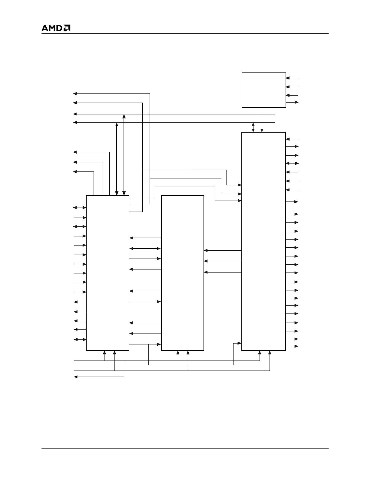
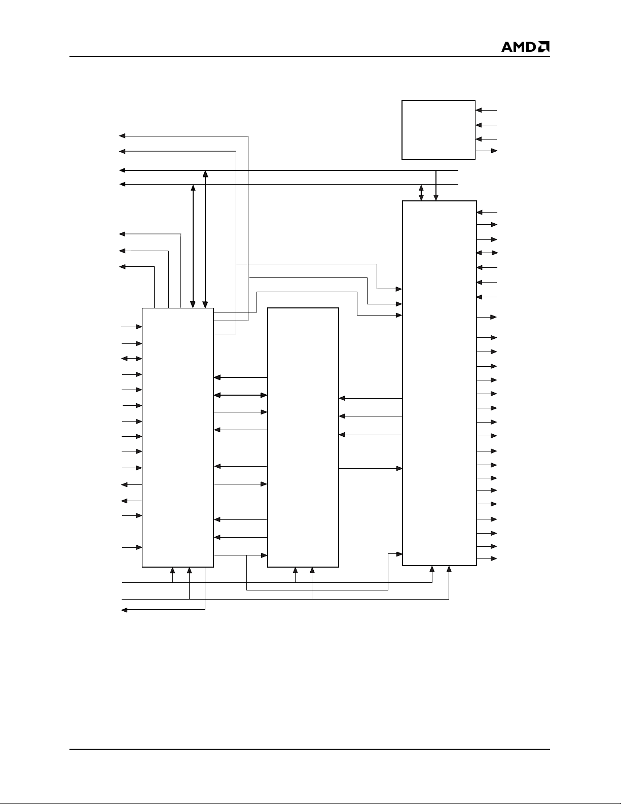
BLOCK DIAGRAM
PCMCIA Mode
PRELIMINARY
MOE
MWE
MA 16–0
MD 7–0
XCE
SCE
FCE
USER6–0
A14–0
D7–0
REG
CE1
OE
IORD
IOWR
RESET
WE
WAIT
INPACK
IREQ
STSCHG
PMX2–1
Bus
Interface
Unit
(PCMCIA)
CA16–8
CAD 7–0
INT1
ALE
WR
SRDY
UCS
LCS
RESET
MAC
Control
Unit
(80188 core)
DRQ0
DRQ1
INT0
JTAG
Control
Block
Transceiver
Attachment
Interface
TRST
TMS/T3
TDI/T1
TDO/T2
RXCIN
ANTSLT
ANTSLT
SAR6–0
ADIN2–1
ADREF
RXDATA
RXC
SDCLK
SDDATA
SDSEL3–1
TXCMD
TXCMD
TXMOD
TXDATA
TXDATA
RXPE
TXPE
HFPE
HFCLK
LFPE
LFCLK
FDET
LNK
ACT
CLKIN
TEST
PWRDWN
20183B-1
Am79C930 3
Page 4
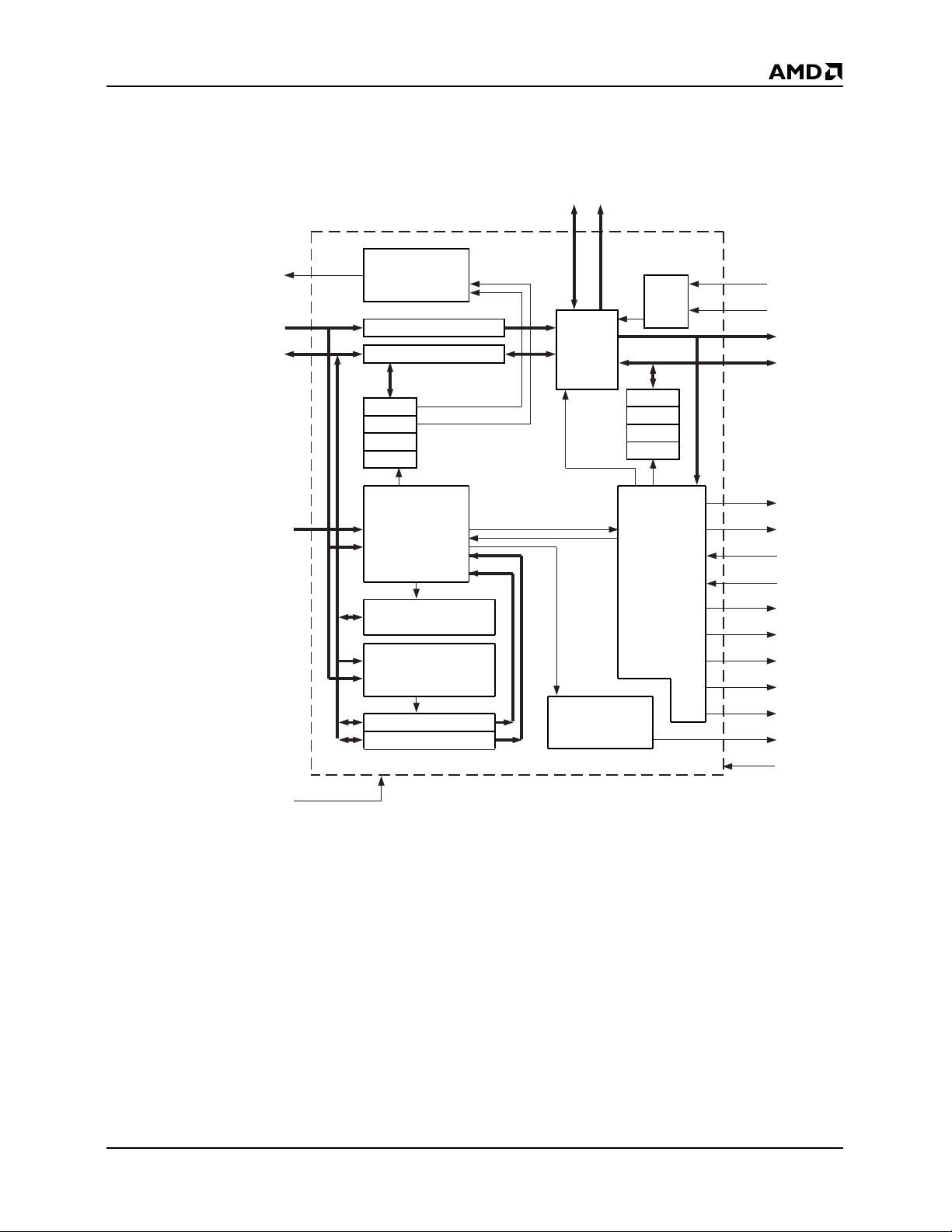
BLOCK DIAGRAM
Bus Interface Unit
IREQ
A14–0 or
LA23–17, SA16–0
D7–0
PRELIMINARY
MD[7:0] MA[16:0]
System
Interrupt
Generator
Address Buffer
Data Buffer
Bus
Multiplexer
Latch
CA16
ALE
CA15–8
CAD7–0
PCMCIA
or
ISA Control Signals
CLKIN
SIR0
SIR1
...
SIR7
Slave
Control
PCMCIA
and ISA
Memory
and I/O
PCMCIA
Config Registers
Plug and Play
Control Module
ISA Memory Base
ISA I/O Base
80188
Interrupt
Generator
MIR0
MIR1
...
MIR15
Slave
Control
and
Arbitration
for
Memory
Interface
Bus
MOE
MWE
UCS
LCS
SRDY
XCE
FCE
TAICE
SCE
INT1
RESET
20183B-2
4 Am79C930
Page 5
PRELIMINARY
BLOCK DIAGRAM
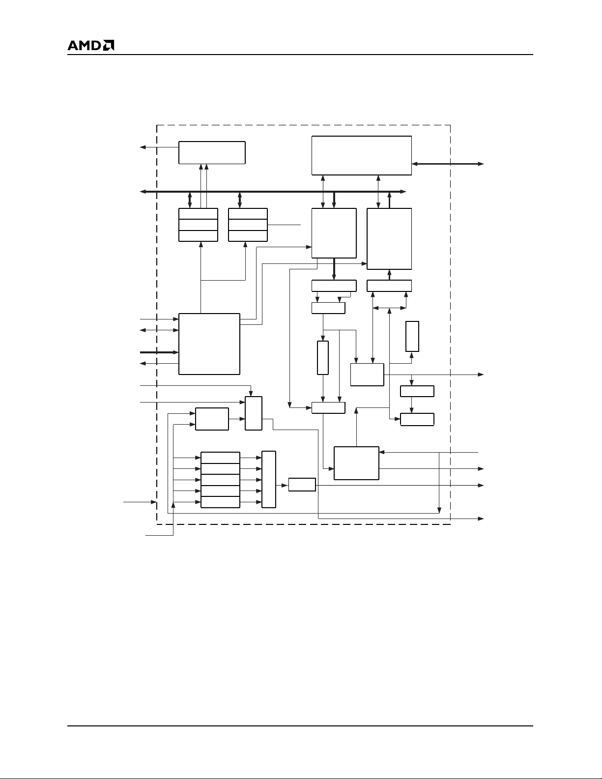
Transceiver Attachment Interface Unit
IRQ
MD[7:0]
TAICE
Slave
Control
MA[4:0]
DRQ[1:0]
RXCSEL
RXCIN
Interrupt
Generator
TIR0
TIR31
Slave
Control
Memory
Interface
Bus I/O
and DMA
DPLL
TCR0
TCR...TIR...
TCR31
C
M
U
X
Empty
Transceiver Interface
Unit Control
TX
FIFO
8
Bytes
P->S S->P
MUX
C
R
C
MUX
FIFO
Bytes
SFD
Detect
Transceiver
Control
Signals
RX
15
C
R
C
FDET
Count
Phylen
RESET
CLKIN
÷80
÷40
÷5
÷10
÷20
M
U
X
Sleep
BIAS
Suppress
RXD
TXD
TXC
RXC
20183B-3
Am79C930 5
Page 6

AMD
P R E L I M I N A R Y
TABLE OF CONTENTS
DISTINCTIVE CHARACTERISTICS 1. . . . . . . . . . . . . . . . . . . . . . . . . . . . . . . . . . . . . . . . . . . . . . . . . . . . . . . .
GENERAL DESCRIPTION 1. . . . . . . . . . . . . . . . . . . . . . . . . . . . . . . . . . . . . . . . . . . . . . . . . . . . . . . . . . . . . . .
ORDERING INFORMATION 2. . . . . . . . . . . . . . . . . . . . . . . . . . . . . . . . . . . . . . . . . . . . . . . . . . . . . . . . . . . . . .
BLOCK DIAGRAM 3. . . . . . . . . . . . . . . . . . . . . . . . . . . . . . . . . . . . . . . . . . . . . . . . . . . . . . . . . . . . . . . . . . . . .
PCMCIA Mode 3. . . . . . . . . . . . . . . . . . . . . . . . . . . . . . . . . . . . . . . . . . . . . . . . . . . . . . . . . . . . . . . . . . . . . .
Bus Interface Unit 4. . . . . . . . . . . . . . . . . . . . . . . . . . . . . . . . . . . . . . . . . . . . . . . . . . . . . . . . . . . . . . . . . . . .
Transceiver Attachment Interface Unit 5. . . . . . . . . . . . . . . . . . . . . . . . . . . . . . . . . . . . . . . . . . . . . . . . . . . .
PCMCIA BLOCK DIAGRAM 12. . . . . . . . . . . . . . . . . . . . . . . . . . . . . . . . . . . . . . . . . . . . . . . . . . . . . . . . . . . .
PCMCIA CONNECTION DIAGRAM 13. . . . . . . . . . . . . . . . . . . . . . . . . . . . . . . . . . . . . . . . . . . . . . . . . . . . . . .
PCMCIA PIN SUMMARY 14. . . . . . . . . . . . . . . . . . . . . . . . . . . . . . . . . . . . . . . . . . . . . . . . . . . . . . . . . . . . . . .
Listed By Pin Number 14. . . . . . . . . . . . . . . . . . . . . . . . . . . . . . . . . . . . . . . . . . . . . . . . . . . . . . . . . . . . . . .
PCMCIA PIN LIST 15. . . . . . . . . . . . . . . . . . . . . . . . . . . . . . . . . . . . . . . . . . . . . . . . . . . . . . . . . . . . . . . . . . . .
Listed By Pin Name 15. . . . . . . . . . . . . . . . . . . . . . . . . . . . . . . . . . . . . . . . . . . . . . . . . . . . . . . . . . . . . . . . .
PCMCIA PIN FUNCTION SUMMARY 16. . . . . . . . . . . . . . . . . . . . . . . . . . . . . . . . . . . . . . . . . . . . . . . . . . . . .
PCMCIA Pin Summary 16. . . . . . . . . . . . . . . . . . . . . . . . . . . . . . . . . . . . . . . . . . . . . . . . . . . . . . . . . . . . . . .
ISA PLUG AND PLAY BLOCK DIAGRAM 19. . . . . . . . . . . . . . . . . . . . . . . . . . . . . . . . . . . . . . . . . . . . . . . . .
CONNECTION DIAGRAM 20. . . . . . . . . . . . . . . . . . . . . . . . . . . . . . . . . . . . . . . . . . . . . . . . . . . . . . . . . . . . . .
ISA Plug And Play 20. . . . . . . . . . . . . . . . . . . . . . . . . . . . . . . . . . . . . . . . . . . . . . . . . . . . . . . . . . . . . . . . . .
ISA PLUG AND PLAY PIN LIST 21. . . . . . . . . . . . . . . . . . . . . . . . . . . . . . . . . . . . . . . . . . . . . . . . . . . . . . . . .
Listed By Pin Number 21. . . . . . . . . . . . . . . . . . . . . . . . . . . . . . . . . . . . . . . . . . . . . . . . . . . . . . . . . . . . . . .
Listed By Pin Name 22. . . . . . . . . . . . . . . . . . . . . . . . . . . . . . . . . . . . . . . . . . . . . . . . . . . . . . . . . . . . . . . . .
ISA PLUG AND PLAY PIN SUMMARY 23. . . . . . . . . . . . . . . . . . . . . . . . . . . . . . . . . . . . . . . . . . . . . . . . . . . .
PIN DESCRIPTIONS 25. . . . . . . . . . . . . . . . . . . . . . . . . . . . . . . . . . . . . . . . . . . . . . . . . . . . . . . . . . . . . . . . . .
Pins with Internal Pull Up or Pull Down Devices 25. . . . . . . . . . . . . . . . . . . . . . . . . . . . . . . . . . . . . . . . . . .
Configuration Pins 25. . . . . . . . . . . . . . . . . . . . . . . . . . . . . . . . . . . . . . . . . . . . . . . . . . . . . . . . . . . . . . . . . .
Host System Interface Pins 25. . . . . . . . . . . . . . . . . . . . . . . . . . . . . . . . . . . . . . . . . . . . . . . . . . . . . . . . . . .
PCMCIA Bus Interface 26. . . . . . . . . . . . . . . . . . . . . . . . . . . . . . . . . . . . . . . . . . . . . . . . . . . . . . . . . . . .
ISA (IEEE P996) Bus interface 27. . . . . . . . . . . . . . . . . . . . . . . . . . . . . . . . . . . . . . . . . . . . . . . . . . . . . .
Memory Interface Pins 26. . . . . . . . . . . . . . . . . . . . . . . . . . . . . . . . . . . . . . . . . . . . . . . . . . . . . . . . . . . .
Clock Pins 29. . . . . . . . . . . . . . . . . . . . . . . . . . . . . . . . . . . . . . . . . . . . . . . . . . . . . . . . . . . . . . . . . . . . . .
System Management Pins 29. . . . . . . . . . . . . . . . . . . . . . . . . . . . . . . . . . . . . . . . . . . . . . . . . . . . . . . . .
TAI Interface Pins 29. . . . . . . . . . . . . . . . . . . . . . . . . . . . . . . . . . . . . . . . . . . . . . . . . . . . . . . . . . . . . . . .
Other Pins 31. . . . . . . . . . . . . . . . . . . . . . . . . . . . . . . . . . . . . . . . . . . . . . . . . . . . . . . . . . . . . . . . . . . . . .
IEEE 1149.1 Test Access Port Pins 32. . . . . . . . . . . . . . . . . . . . . . . . . . . . . . . . . . . . . . . . . . . . . . . . . .
Power Supply Pins 32. . . . . . . . . . . . . . . . . . . . . . . . . . . . . . . . . . . . . . . . . . . . . . . . . . . . . . . . . . . . . . .
Analog Power Supply Pins 32. . . . . . . . . . . . . . . . . . . . . . . . . . . . . . . . . . . . . . . . . . . . . . . . . . . . . . .
Digital Power Supply Pins 32. . . . . . . . . . . . . . . . . . . . . . . . . . . . . . . . . . . . . . . . . . . . . . . . . . . . . . .
Multi-Function Pins 33. . . . . . . . . . . . . . . . . . . . . . . . . . . . . . . . . . . . . . . . . . . . . . . . . . . . . . . . . . . . . . .
Pin 1: USER2/LA19 34. . . . . . . . . . . . . . . . . . . . . . . . . . . . . . . . . . . . . . . . . . . . . . . . . . . . . . . . . . . .
Pin 2: USER3/SA16 34. . . . . . . . . . . . . . . . . . . . . . . . . . . . . . . . . . . . . . . . . . . . . . . . . . . . . . . . . . . .
6
Am79C930
Page 7

P R E L I M I N A R Y
AMD
Pin 3: USER4/LA17 34. . . . . . . . . . . . . . . . . . . . . . . . . . . . . . . . . . . . . . . . . . . . . . . . . . . . . . . . . . . .
Pin 45: STSCHG/BALE 34. . . . . . . . . . . . . . . . . . . . . . . . . . . . . . . . . . . . . . . . . . . . . . . . . . . . . . . . .
Pin 90: USER0/RFRSH 34. . . . . . . . . . . . . . . . . . . . . . . . . . . . . . . . . . . . . . . . . . . . . . . . . . . . . . . . .
Pin 91: USER1/IRQ12/EXTCTS/EXINT188 35. . . . . . . . . . . . . . . . . . . . . . . . . . . . . . . . . . . . . . . . . .
Pin 92: USER7/IRQ11 35. . . . . . . . . . . . . . . . . . . . . . . . . . . . . . . . . . . . . . . . . . . . . . . . . . . . . . . . . .
Pin 94: RXC/IRQ10/EXTA2DST 36. . . . . . . . . . . . . . . . . . . . . . . . . . . . . . . . . . . . . . . . . . . . . . . . . .
Pin 95: USER6/IRQ5/EXTSDF 36. . . . . . . . . . . . . . . . . . . . . . . . . . . . . . . . . . . . . . . . . . . . . . . . . . .
Pin 96: USER5/IRQ4/EXTCHBSY 36. . . . . . . . . . . . . . . . . . . . . . . . . . . . . . . . . . . . . . . . . . . . . . . . .
Pin 98: ACT 37. . . . . . . . . . . . . . . . . . . . . . . . . . . . . . . . . . . . . . . . . . . . . . . . . . . . . . . . . . . . . . . . . .
Pin 100: LNK 37. . . . . . . . . . . . . . . . . . . . . . . . . . . . . . . . . . . . . . . . . . . . . . . . . . . . . . . . . . . . . . . . .
Pin 101: SDCLK 38. . . . . . . . . . . . . . . . . . . . . . . . . . . . . . . . . . . . . . . . . . . . . . . . . . . . . . . . . . . . . . .
Pin 102: SDDATA 38. . . . . . . . . . . . . . . . . . . . . . . . . . . . . . . . . . . . . . . . . . . . . . . . . . . . . . . . . . . . .
Pin 103: SDSEL3 38. . . . . . . . . . . . . . . . . . . . . . . . . . . . . . . . . . . . . . . . . . . . . . . . . . . . . . . . . . . . . .
Pin 105: SDSEL2 38. . . . . . . . . . . . . . . . . . . . . . . . . . . . . . . . . . . . . . . . . . . . . . . . . . . . . . . . . . . . . .
Pin 107: SDSEL1 38. . . . . . . . . . . . . . . . . . . . . . . . . . . . . . . . . . . . . . . . . . . . . . . . . . . . . . . . . . . . . .
Pin 115: TXC 39. . . . . . . . . . . . . . . . . . . . . . . . . . . . . . . . . . . . . . . . . . . . . . . . . . . . . . . . . . . . . . . . .
Pin 118: LFPE 39. . . . . . . . . . . . . . . . . . . . . . . . . . . . . . . . . . . . . . . . . . . . . . . . . . . . . . . . . . . . . . . .
Pin 120: HFPE 39. . . . . . . . . . . . . . . . . . . . . . . . . . . . . . . . . . . . . . . . . . . . . . . . . . . . . . . . . . . . . . . .
Pin 122: RXPE 39. . . . . . . . . . . . . . . . . . . . . . . . . . . . . . . . . . . . . . . . . . . . . . . . . . . . . . . . . . . . . . . .
Pin 126: TXCMD 40. . . . . . . . . . . . . . . . . . . . . . . . . . . . . . . . . . . . . . . . . . . . . . . . . . . . . . . . . . . . . .
Pin 129: TXPE 40. . . . . . . . . . . . . . . . . . . . . . . . . . . . . . . . . . . . . . . . . . . . . . . . . . . . . . . . . . . . . . . .
Pin 131: TXMOD 40. . . . . . . . . . . . . . . . . . . . . . . . . . . . . . . . . . . . . . . . . . . . . . . . . . . . . . . . . . . . . .
Pin 132: ANTSLT 40. . . . . . . . . . . . . . . . . . . . . . . . . . . . . . . . . . . . . . . . . . . . . . . . . . . . . . . . . . . . . .
Pin 141: ANTSLT/LA23 40. . . . . . . . . . . . . . . . . . . . . . . . . . . . . . . . . . . . . . . . . . . . . . . . . . . . . . . . .
Pin 142: TXCMD/LA21 41. . . . . . . . . . . . . . . . . . . . . . . . . . . . . . . . . . . . . . . . . . . . . . . . . . . . . . . . . .
Pin 143: TXDATA/LA20 41. . . . . . . . . . . . . . . . . . . . . . . . . . . . . . . . . . . . . . . . . . . . . . . . . . . . . . . . .
Pin 144: LLOCKE/SA15 41. . . . . . . . . . . . . . . . . . . . . . . . . . . . . . . . . . . . . . . . . . . . . . . . . . . . . . . . .
FUNCTIONAL DESCRIPTION 42. . . . . . . . . . . . . . . . . . . . . . . . . . . . . . . . . . . . . . . . . . . . . . . . . . . . . . . . . . .
Basic Functions 42. . . . . . . . . . . . . . . . . . . . . . . . . . . . . . . . . . . . . . . . . . . . . . . . . . . . . . . . . . . . . . . . . . . .
System Bus Interface Function 42. . . . . . . . . . . . . . . . . . . . . . . . . . . . . . . . . . . . . . . . . . . . . . . . . . . . . .
Memory Bus Interface Function 42. . . . . . . . . . . . . . . . . . . . . . . . . . . . . . . . . . . . . . . . . . . . . . . . . . . . .
Software Interface Function 42. . . . . . . . . . . . . . . . . . . . . . . . . . . . . . . . . . . . . . . . . . . . . . . . . . . . . . . .
Network Interface Function 42. . . . . . . . . . . . . . . . . . . . . . . . . . . . . . . . . . . . . . . . . . . . . . . . . . . . . . . . .
Detailed Functions 42. . . . . . . . . . . . . . . . . . . . . . . . . . . . . . . . . . . . . . . . . . . . . . . . . . . . . . . . . . . . . . . . . .
Block Level Description 42. . . . . . . . . . . . . . . . . . . . . . . . . . . . . . . . . . . . . . . . . . . . . . . . . . . . . . . . . . . .
Bus Interface Unit 42. . . . . . . . . . . . . . . . . . . . . . . . . . . . . . . . . . . . . . . . . . . . . . . . . . . . . . . . . . . . .
PCMCIA Interface 43. . . . . . . . . . . . . . . . . . . . . . . . . . . . . . . . . . . . . . . . . . . . . . . . . . . . . . . . . . .
ISA (IEEE P996) Plug and Play Interface 44. . . . . . . . . . . . . . . . . . . . . . . . . . . . . . . . . . . . . . . . .
Memory Interface 45. . . . . . . . . . . . . . . . . . . . . . . . . . . . . . . . . . . . . . . . . . . . . . . . . . . . . . . . . . . . . .
Embedded 80188 45. . . . . . . . . . . . . . . . . . . . . . . . . . . . . . . . . . . . . . . . . . . . . . . . . . . . . . . . . . . . . .
Media Access Management 45. . . . . . . . . . . . . . . . . . . . . . . . . . . . . . . . . . . . . . . . . . . . . . . . . . .
Medium Allocation 46. . . . . . . . . . . . . . . . . . . . . . . . . . . . . . . . . . . . . . . . . . . . . . . . . . . . . . . . . .
Initialization 46. . . . . . . . . . . . . . . . . . . . . . . . . . . . . . . . . . . . . . . . . . . . . . . . . . . . . . . . . . . . . . . .
SRAM Memory Management 46. . . . . . . . . . . . . . . . . . . . . . . . . . . . . . . . . . . . . . . . . . . . . . . . . .
Flash Memory Management 47. . . . . . . . . . . . . . . . . . . . . . . . . . . . . . . . . . . . . . . . . . . . . . . . . . .
Transceiver Attachment Interface Unit Management 47. . . . . . . . . . . . . . . . . . . . . . . . . . . . . . . .
7Am79C930
Page 8

AMD
P R E L I M I N A R Y
Bus Interface Unit Interaction 47. . . . . . . . . . . . . . . . . . . . . . . . . . . . . . . . . . . . . . . . . . . . . . . . . .
Transceiver Attachment Interface Unit 47. . . . . . . . . . . . . . . . . . . . . . . . . . . . . . . . . . . . . . . . . . . . . .
TX FIFO 48. . . . . . . . . . . . . . . . . . . . . . . . . . . . . . . . . . . . . . . . . . . . . . . . . . . . . . . . . . . . . . . . . .
TX Power Ramp Control 48. . . . . . . . . . . . . . . . . . . . . . . . . . . . . . . . . . . . . . . . . . . . . . . . . . . . . .
Am79C930-based TX Power Ramp Control . 48. . . . . . . . . . . . . . . . . . . . . . . . . . . . . . . . . . .
Transceiver-Based TX Power Ramp Control . 50. . . . . . . . . . . . . . . . . . . . . . . . . . . . . . . . . .
TX CRC Generation 50. . . . . . . . . . . . . . . . . . . . . . . . . . . . . . . . . . . . . . . . . . . . . . . . . . . . . . . . .
TX Status 50. . . . . . . . . . . . . . . . . . . . . . . . . . . . . . . . . . . . . . . . . . . . . . . . . . . . . . . . . . . . . . . . .
Start of Frame Delimiter Detection 50. . . . . . . . . . . . . . . . . . . . . . . . . . . . . . . . . . . . . . . . . . . . . .
RX Data Parallelization 50. . . . . . . . . . . . . . . . . . . . . . . . . . . . . . . . . . . . . . . . . . . . . . . . . . . . . . .
RX FIFO 50. . . . . . . . . . . . . . . . . . . . . . . . . . . . . . . . . . . . . . . . . . . . . . . . . . . . . . . . . . . . . . . . . .
RX CRC Checking 50. . . . . . . . . . . . . . . . . . . . . . . . . . . . . . . . . . . . . . . . . . . . . . . . . . . . . . . . . .
RX Status Reporting 51. . . . . . . . . . . . . . . . . . . . . . . . . . . . . . . . . . . . . . . . . . . . . . . . . . . . . . . . .
Bit Ordering 51. . . . . . . . . . . . . . . . . . . . . . . . . . . . . . . . . . . . . . . . . . . . . . . . . . . . . . . . . . . . . . .
RSSI A/D Unit 51. . . . . . . . . . . . . . . . . . . . . . . . . . . . . . . . . . . . . . . . . . . . . . . . . . . . . . . . . . . . . .
Physical Header Accommodation 52. . . . . . . . . . . . . . . . . . . . . . . . . . . . . . . . . . . . . . . . . . . . . . .
DC Bias Control 52. . . . . . . . . . . . . . . . . . . . . . . . . . . . . . . . . . . . . . . . . . . . . . . . . . . . . . . . . . . .
Baud Determination Logic 52. . . . . . . . . . . . . . . . . . . . . . . . . . . . . . . . . . . . . . . . . . . . . . . . . . . .
Clear Channel Assessment Logic 53. . . . . . . . . . . . . . . . . . . . . . . . . . . . . . . . . . . . . . . . . . . . . . .
Automatic Antenna Diversity Logic 54. . . . . . . . . . . . . . . . . . . . . . . . . . . . . . . . . . . . . . . . . . . . . .
TXC As Input 55. . . . . . . . . . . . . . . . . . . . . . . . . . . . . . . . . . . . . . . . . . . . . . . . . . . . . . . . . . . . . .
IEEE 1149.1 Test Access Port Interface 55. . . . . . . . . . . . . . . . . . . . . . . . . . . . . . . . . . . . . . . . . . . .
Boundary Scan Circuit 56. . . . . . . . . . . . . . . . . . . . . . . . . . . . . . . . . . . . . . . . . . . . . . . . . . . . . . .
TAP FSM 56. . . . . . . . . . . . . . . . . . . . . . . . . . . . . . . . . . . . . . . . . . . . . . . . . . . . . . . . . . . . . . . . .
Supported Instructions 56. . . . . . . . . . . . . . . . . . . . . . . . . . . . . . . . . . . . . . . . . . . . . . . . . . . . . . .
Instruction Register and Decoding Logic 56. . . . . . . . . . . . . . . . . . . . . . . . . . . . . . . . . . . . . . . . .
Boundary Scan Register (BSR) 56. . . . . . . . . . . . . . . . . . . . . . . . . . . . . . . . . . . . . . . . . . . . . . . .
Other Data Registers 56. . . . . . . . . . . . . . . . . . . . . . . . . . . . . . . . . . . . . . . . . . . . . . . . . . . . . . . .
Power Saving Modes 56. . . . . . . . . . . . . . . . . . . . . . . . . . . . . . . . . . . . . . . . . . . . . . . . . . . . . . . . . . .
Power Down Function 56. . . . . . . . . . . . . . . . . . . . . . . . . . . . . . . . . . . . . . . . . . . . . . . . . . . . . . . .
Applicability to IEEE 802.11 Power Down Modes 58. . . . . . . . . . . . . . . . . . . . . . . . . . . . . . . . . .
Software Access 58. . . . . . . . . . . . . . . . . . . . . . . . . . . . . . . . . . . . . . . . . . . . . . . . . . . . . . . . . . . . . . . . .
Am79C930 System Interface Resources 58. . . . . . . . . . . . . . . . . . . . . . . . . . . . . . . . . . . . . . . . . . . .
PCMCIA Mode Resources 58. . . . . . . . . . . . . . . . . . . . . . . . . . . . . . . . . . . . . . . . . . . . . . . . . . . .
PCMCIA Attribute Memory Resources. 61. . . . . . . . . . . . . . . . . . . . . . . . . . . . . . . . . . . . . . . .
PCMCIA I/O Resources. 62. . . . . . . . . . . . . . . . . . . . . . . . . . . . . . . . . . . . . . . . . . . . . . . . . . .
ISA Plug and Play Mode Resources 63. . . . . . . . . . . . . . . . . . . . . . . . . . . . . . . . . . . . . . . . . . . . .
ISA Plug and Play Memory Resources 64. . . . . . . . . . . . . . . . . . . . . . . . . . . . . . . . . . . . . . . .
ISA Plug and Play I/O Resources. 66. . . . . . . . . . . . . . . . . . . . . . . . . . . . . . . . . . . . . . . . . . . .
ISA Plug and Play Register Set. 68. . . . . . . . . . . . . . . . . . . . . . . . . . . . . . . . . . . . . . . . . . . . .
MAC Firmware Resources 70. . . . . . . . . . . . . . . . . . . . . . . . . . . . . . . . . . . . . . . . . . . . . . . . . . . . . . .
MAC (80188 core) Memory Resources 70. . . . . . . . . . . . . . . . . . . . . . . . . . . . . . . . . . . . . . . . . .
MAC (80188 core) Memory Resources Restrictions 72. . . . . . . . . . . . . . . . . . . . . . . . . . . . . . . .
MAC (80188 core) Interrupt Channel Allocation 72. . . . . . . . . . . . . . . . . . . . . . . . . . . . . . . . . . . .
MAC (80188 core) DMA Channel Allocation 72. . . . . . . . . . . . . . . . . . . . . . . . . . . . . . . . . . . . . .
DMA Channel Allocation In The 80188 Core 73. . . . . . . . . . . . . . . . . . . . . . . . . . . . . . . . . . . . . .
Loopback Operation 73. . . . . . . . . . . . . . . . . . . . . . . . . . . . . . . . . . . . . . . . . . . . . . . . . . . . . . . . . . . . . .
8
Am79C930
Page 9

P R E L I M I N A R Y
AMD
LED Support 73. . . . . . . . . . . . . . . . . . . . . . . . . . . . . . . . . . . . . . . . . . . . . . . . . . . . . . . . . . . . . . . . . . . .
RESET Methods 73. . . . . . . . . . . . . . . . . . . . . . . . . . . . . . . . . . . . . . . . . . . . . . . . . . . . . . . . . . . . . . . . .
RESET Pin 73. . . . . . . . . . . . . . . . . . . . . . . . . . . . . . . . . . . . . . . . . . . . . . . . . . . . . . . . . . . . . . . . . . .
SWRESET (SIR0[7]) 73. . . . . . . . . . . . . . . . . . . . . . . . . . . . . . . . . . . . . . . . . . . . . . . . . . . . . . . . . . .
CORESET (SIR0[6]) 74. . . . . . . . . . . . . . . . . . . . . . . . . . . . . . . . . . . . . . . . . . . . . . . . . . . . . . . . . . .
PCMCIA COR SRESET 74. . . . . . . . . . . . . . . . . . . . . . . . . . . . . . . . . . . . . . . . . . . . . . . . . . . . . . . .
ISA PnP RESET 75. . . . . . . . . . . . . . . . . . . . . . . . . . . . . . . . . . . . . . . . . . . . . . . . . . . . . . . . . . . . . .
SRES (TIR0[5]) 75. . . . . . . . . . . . . . . . . . . . . . . . . . . . . . . . . . . . . . . . . . . . . . . . . . . . . . . . . . . . . . .
REGISTER DESCRIPTIONS 75. . . . . . . . . . . . . . . . . . . . . . . . . . . . . . . . . . . . . . . . . . . . . . . . . . . . . . . . . . . .
System Interface Registers (SIR space) 76. . . . . . . . . . . . . . . . . . . . . . . . . . . . . . . . . . . . . . . . . . . . . . . . .
SIR0: General Configuration Register (GCR) 77. . . . . . . . . . . . . . . . . . . . . . . . . . . . . . . . . . . . . . . . . . .
SIR1: Bank Switching Select Register (BSS) 78. . . . . . . . . . . . . . . . . . . . . . . . . . . . . . . . . . . . . . . . . . .
SIR2: Local Memory Address Register [7:0] (LMA) 79. . . . . . . . . . . . . . . . . . . . . . . . . . . . . . . . . . . . . .
SIR3: Local Memory Address Register [14:8] (LMA) 79. . . . . . . . . . . . . . . . . . . . . . . . . . . . . . . . . . . . .
SIR4: I/O Data Port A (IODPA) 79. . . . . . . . . . . . . . . . . . . . . . . . . . . . . . . . . . . . . . . . . . . . . . . . . . . . . .
SIR5: I/O Data Port B (IODPB) 80. . . . . . . . . . . . . . . . . . . . . . . . . . . . . . . . . . . . . . . . . . . . . . . . . . . . . .
SIR6: I/O Data Port C (IODPC) 80. . . . . . . . . . . . . . . . . . . . . . . . . . . . . . . . . . . . . . . . . . . . . . . . . . . . . .
SIR7: I/O Data Port D (IODPD) 80. . . . . . . . . . . . . . . . . . . . . . . . . . . . . . . . . . . . . . . . . . . . . . . . . . . . . .
MAC Interface Registers (MIR Space) 80. . . . . . . . . . . . . . . . . . . . . . . . . . . . . . . . . . . . . . . . . . . . . . . . . . .
MIR0: Processor Interface Register (PIR) 80. . . . . . . . . . . . . . . . . . . . . . . . . . . . . . . . . . . . . . . . . . . . .
MIR1: Power Up Clock Time [3:0] (PUCT) 81. . . . . . . . . . . . . . . . . . . . . . . . . . . . . . . . . . . . . . . . . . . . .
MIR2: Power Down Length Count [7:0] (PDLC) 81. . . . . . . . . . . . . . . . . . . . . . . . . . . . . . . . . . . . . . . . .
MIR3: Power Down Length Count [15:8] (PDLC) 81. . . . . . . . . . . . . . . . . . . . . . . . . . . . . . . . . . . . . . . .
MIR4: Power Down Length Count [22:16] (PDLC) 82. . . . . . . . . . . . . . . . . . . . . . . . . . . . . . . . . . . . . . .
MIR5: Free Count [7:0] (FCNT) 82. . . . . . . . . . . . . . . . . . . . . . . . . . . . . . . . . . . . . . . . . . . . . . . . . . . . .
MIR6: Free Count [15:8] (FCNT) 82. . . . . . . . . . . . . . . . . . . . . . . . . . . . . . . . . . . . . . . . . . . . . . . . . . . .
MIR7: Free Count [23:16] (FCNT) 82. . . . . . . . . . . . . . . . . . . . . . . . . . . . . . . . . . . . . . . . . . . . . . . . . . .
MIR8: Flash Wait States 82. . . . . . . . . . . . . . . . . . . . . . . . . . . . . . . . . . . . . . . . . . . . . . . . . . . . . . . . . . .
MIR9: TCR Mask STSCHG Data 83. . . . . . . . . . . . . . . . . . . . . . . . . . . . . . . . . . . . . . . . . . . . . . . . . . . .
MIR10: Reserved 85. . . . . . . . . . . . . . . . . . . . . . . . . . . . . . . . . . . . . . . . . . . . . . . . . . . . . . . . . . . . . . . .
MIR11: Reserved 85. . . . . . . . . . . . . . . . . . . . . . . . . . . . . . . . . . . . . . . . . . . . . . . . . . . . . . . . . . . . . . . .
MIR12: Reserved 85. . . . . . . . . . . . . . . . . . . . . . . . . . . . . . . . . . . . . . . . . . . . . . . . . . . . . . . . . . . . . . . .
MIR13: Reserved 85. . . . . . . . . . . . . . . . . . . . . . . . . . . . . . . . . . . . . . . . . . . . . . . . . . . . . . . . . . . . . . . .
MIR14: Reserved 85. . . . . . . . . . . . . . . . . . . . . . . . . . . . . . . . . . . . . . . . . . . . . . . . . . . . . . . . . . . . . . . .
MIR15: Reserved 85. . . . . . . . . . . . . . . . . . . . . . . . . . . . . . . . . . . . . . . . . . . . . . . . . . . . . . . . . . . . . . . .
Transceiver Attachment Interface Registers (TIR Space) 86. . . . . . . . . . . . . . . . . . . . . . . . . . . . . . . . . . . .
TIR0: Network Control 89. . . . . . . . . . . . . . . . . . . . . . . . . . . . . . . . . . . . . . . . . . . . . . . . . . . . . . . . . . . .
TIR1: Network Status 89. . . . . . . . . . . . . . . . . . . . . . . . . . . . . . . . . . . . . . . . . . . . . . . . . . . . . . . . . . . . .
TIR2: Serial Device 90. . . . . . . . . . . . . . . . . . . . . . . . . . . . . . . . . . . . . . . . . . . . . . . . . . . . . . . . . . . . . . .
TIR3: Fast Serial Port Control 91. . . . . . . . . . . . . . . . . . . . . . . . . . . . . . . . . . . . . . . . . . . . . . . . . . . . . . .
TIR4: Interrupt Register 1 91. . . . . . . . . . . . . . . . . . . . . . . . . . . . . . . . . . . . . . . . . . . . . . . . . . . . . . . . . .
TIR5: Interrupt Register 92. . . . . . . . . . . . . . . . . . . . . . . . . . . . . . . . . . . . . . . . . . . . . . . . . . . . . . . . . . .
TIR6: Interrupt Unmask Register 1 93. . . . . . . . . . . . . . . . . . . . . . . . . . . . . . . . . . . . . . . . . . . . . . . . . . .
TIR7: Interrupt Unmask Register 2 93. . . . . . . . . . . . . . . . . . . . . . . . . . . . . . . . . . . . . . . . . . . . . . . . . . .
TIR8: Transmit Control 94. . . . . . . . . . . . . . . . . . . . . . . . . . . . . . . . . . . . . . . . . . . . . . . . . . . . . . . . . . . .
TIR9: Transmit Status 94. . . . . . . . . . . . . . . . . . . . . . . . . . . . . . . . . . . . . . . . . . . . . . . . . . . . . . . . . . . . .
9Am79C930
Page 10

AMD
P R E L I M I N A R Y
TIR10: TX FIFO Data Register 95. . . . . . . . . . . . . . . . . . . . . . . . . . . . . . . . . . . . . . . . . . . . . . . . . . . . . .
TIR11: Transmit Sequence Control 95. . . . . . . . . . . . . . . . . . . . . . . . . . . . . . . . . . . . . . . . . . . . . . . . . . .
TIR12: Byte Count Register LSB 96. . . . . . . . . . . . . . . . . . . . . . . . . . . . . . . . . . . . . . . . . . . . . . . . . . . .
TIR13: Byte Count Register MSB 97. . . . . . . . . . . . . . . . . . . . . . . . . . . . . . . . . . . . . . . . . . . . . . . . . . . .
TIR14: Byte Count Limit LSB 97. . . . . . . . . . . . . . . . . . . . . . . . . . . . . . . . . . . . . . . . . . . . . . . . . . . . . . .
TIR15: Byte Count Limit MSB 97. . . . . . . . . . . . . . . . . . . . . . . . . . . . . . . . . . . . . . . . . . . . . . . . . . . . . . .
TIR16: Receiver Control 98. . . . . . . . . . . . . . . . . . . . . . . . . . . . . . . . . . . . . . . . . . . . . . . . . . . . . . . . . . .
TIR17: Receive Status Register 98. . . . . . . . . . . . . . . . . . . . . . . . . . . . . . . . . . . . . . . . . . . . . . . . . . . . .
TIR18: RX FIFO Data Register 99. . . . . . . . . . . . . . . . . . . . . . . . . . . . . . . . . . . . . . . . . . . . . . . . . . . . . .
TIR19: Reserved 98. . . . . . . . . . . . . . . . . . . . . . . . . . . . . . . . . . . . . . . . . . . . . . . . . . . . . . . . . . . . . . . . .
TIR20: CRC32 Correct Byte Count LSB 99. . . . . . . . . . . . . . . . . . . . . . . . . . . . . . . . . . . . . . . . . . . . . . .
TIR21: CRC32 Correct Byte Count MSB 99. . . . . . . . . . . . . . . . . . . . . . . . . . . . . . . . . . . . . . . . . . . . . .
TIR22: CRC8 Correct Byte Count LSB 100. . . . . . . . . . . . . . . . . . . . . . . . . . . . . . . . . . . . . . . . . . . . . . .
TIR23: CRC8 Correct Byte Count MSB 100. . . . . . . . . . . . . . . . . . . . . . . . . . . . . . . . . . . . . . . . . . . . . .
TIR24: TCR Index Register 100. . . . . . . . . . . . . . . . . . . . . . . . . . . . . . . . . . . . . . . . . . . . . . . . . . . . . . . .
TIR25: Configuration Data Port 101. . . . . . . . . . . . . . . . . . . . . . . . . . . . . . . . . . . . . . . . . . . . . . . . . . . . .
TIR26: Antenna Diversity and A/D Control 101. . . . . . . . . . . . . . . . . . . . . . . . . . . . . . . . . . . . . . . . . . . .
TIR27: Serial Approximation Register 102. . . . . . . . . . . . . . . . . . . . . . . . . . . . . . . . . . . . . . . . . . . . . . . .
TIR28: RSSI Lower Limit 102. . . . . . . . . . . . . . . . . . . . . . . . . . . . . . . . . . . . . . . . . . . . . . . . . . . . . . . . .
TIR29: USER Pin Data 103. . . . . . . . . . . . . . . . . . . . . . . . . . . . . . . . . . . . . . . . . . . . . . . . . . . . . . . . . . .
TIR30: Test Dummy Register 103. . . . . . . . . . . . . . . . . . . . . . . . . . . . . . . . . . . . . . . . . . . . . . . . . . . . . .
TIR31: TEST 103. . . . . . . . . . . . . . . . . . . . . . . . . . . . . . . . . . . . . . . . . . . . . . . . . . . . . . . . . . . . . . . . . . .
TAI Configuration Register space (TCR) 103. . . . . . . . . . . . . . . . . . . . . . . . . . . . . . . . . . . . . . . . . . . . . . . .
TCR0: Network Configuration 104. . . . . . . . . . . . . . . . . . . . . . . . . . . . . . . . . . . . . . . . . . . . . . . . . . . . . .
TCR1: Transmit Configuration 104. . . . . . . . . . . . . . . . . . . . . . . . . . . . . . . . . . . . . . . . . . . . . . . . . . . . .
TCR2: Clock Recovery 105. . . . . . . . . . . . . . . . . . . . . . . . . . . . . . . . . . . . . . . . . . . . . . . . . . . . . . . . . . .
TCR3: Receive Configuration 106. . . . . . . . . . . . . . . . . . . . . . . . . . . . . . . . . . . . . . . . . . . . . . . . . . . . . .
TCR4: Antenna Diversity Timer 106. . . . . . . . . . . . . . . . . . . . . . . . . . . . . . . . . . . . . . . . . . . . . . . . . . . .
TCR5: TX Ramp Up Timing 107. . . . . . . . . . . . . . . . . . . . . . . . . . . . . . . . . . . . . . . . . . . . . . . . . . . . . . .
TCR6: TX Ramp Down Timing 108. . . . . . . . . . . . . . . . . . . . . . . . . . . . . . . . . . . . . . . . . . . . . . . . . . . . .
TCR7: Pin Data A 108. . . . . . . . . . . . . . . . . . . . . . . . . . . . . . . . . . . . . . . . . . . . . . . . . . . . . . . . . . . . . . .
TCR8: Start Delimiter LSB 109. . . . . . . . . . . . . . . . . . . . . . . . . . . . . . . . . . . . . . . . . . . . . . . . . . . . . . . .
TCR9: Start Delimiter CSB 110. . . . . . . . . . . . . . . . . . . . . . . . . . . . . . . . . . . . . . . . . . . . . . . . . . . . . . . .
TCR10: Start Delimiter MSB 110. . . . . . . . . . . . . . . . . . . . . . . . . . . . . . . . . . . . . . . . . . . . . . . . . . . . . . .
TCR11: Interrupt Register 3 110. . . . . . . . . . . . . . . . . . . . . . . . . . . . . . . . . . . . . . . . . . . . . . . . . . . . . . .
TCR12: Interrupt Unmask Register 3 111. . . . . . . . . . . . . . . . . . . . . . . . . . . . . . . . . . . . . . . . . . . . . . . .
TCR13: Pin Configuration A 111. . . . . . . . . . . . . . . . . . . . . . . . . . . . . . . . . . . . . . . . . . . . . . . . . . . . . . .
TCR14: Pin Configuration B 112. . . . . . . . . . . . . . . . . . . . . . . . . . . . . . . . . . . . . . . . . . . . . . . . . . . . . . .
TCR15: Pin Configuration C 113. . . . . . . . . . . . . . . . . . . . . . . . . . . . . . . . . . . . . . . . . . . . . . . . . . . . . . .
TCR16: Baud Detect Start 114. . . . . . . . . . . . . . . . . . . . . . . . . . . . . . . . . . . . . . . . . . . . . . . . . . . . . . . .
TCR17: Baud Detect Lower Limit 115. . . . . . . . . . . . . . . . . . . . . . . . . . . . . . . . . . . . . . . . . . . . . . . . . . .
TCR18: Baud Detect Upper Limit. 115. . . . . . . . . . . . . . . . . . . . . . . . . . . . . . . . . . . . . . . . . . . . . . . . . .
TCR19: Baud Detect Accept Count for Carrier Sense 116. . . . . . . . . . . . . . . . . . . . . . . . . . . . . . . . . . .
TCR20: Baud Detect Accept Count for Stop Diversity 116. . . . . . . . . . . . . . . . . . . . . . . . . . . . . . . . . . .
TCR21: Baud Detect Ratio 116. . . . . . . . . . . . . . . . . . . . . . . . . . . . . . . . . . . . . . . . . . . . . . . . . . . . . . . .
TCR22: Baud Detect Accept Count 117. . . . . . . . . . . . . . . . . . . . . . . . . . . . . . . . . . . . . . . . . . . . . . . . .
TCR23: Baud Detect Fail Count 117. . . . . . . . . . . . . . . . . . . . . . . . . . . . . . . . . . . . . . . . . . . . . . . . . . . .
10
Am79C930
Page 11

P R E L I M I N A R Y
AMD
TCR24: RSSI Sample Start 117. . . . . . . . . . . . . . . . . . . . . . . . . . . . . . . . . . . . . . . . . . . . . . . . . . . . . . .
TCR25: RSSI Configuration 118. . . . . . . . . . . . . . . . . . . . . . . . . . . . . . . . . . . . . . . . . . . . . . . . . . . . . . .
TCR26: Reserved 119. . . . . . . . . . . . . . . . . . . . . . . . . . . . . . . . . . . . . . . . . . . . . . . . . . . . . . . . . . . . . . .
TCR27: TIP LED Scramble 120. . . . . . . . . . . . . . . . . . . . . . . . . . . . . . . . . . . . . . . . . . . . . . . . . . . . . . . .
TCR28: Clear Channel Assessment Configuration 121. . . . . . . . . . . . . . . . . . . . . . . . . . . . . . . . . . . . . .
TCR29: Reserved 122. . . . . . . . . . . . . . . . . . . . . . . . . . . . . . . . . . . . . . . . . . . . . . . . . . . . . . . . . . . . . . .
TCR30: Pin Function and Data Rate 122. . . . . . . . . . . . . . . . . . . . . . . . . . . . . . . . . . . . . . . . . . . . . . . . .
TCR31: Device Revision 123. . . . . . . . . . . . . . . . . . . . . . . . . . . . . . . . . . . . . . . . . . . . . . . . . . . . . . . . . .
PCMCIA CCR Registers and PCMCIA CIS Space 124. . . . . . . . . . . . . . . . . . . . . . . . . . . . . . . . . . . . . . . .
PCMCIA Card Configuration and Status Register 124. . . . . . . . . . . . . . . . . . . . . . . . . . . . . . . . . . . . . .
PCMCIA Card Information Structure (CIS) 125. . . . . . . . . . . . . . . . . . . . . . . . . . . . . . . . . . . . . . . . . . . .
ABSOLUTE MAXIMUM RATINGS 126. . . . . . . . . . . . . . . . . . . . . . . . . . . . . . . . . . . . . . . . . . . . . . . . . . . . . . .
OPERATING RANGES 126. . . . . . . . . . . . . . . . . . . . . . . . . . . . . . . . . . . . . . . . . . . . . . . . . . . . . . . . . . . . . . . .
DC CHARACTERISTICS 126. . . . . . . . . . . . . . . . . . . . . . . . . . . . . . . . . . . . . . . . . . . . . . . . . . . . . . . . . . . . . .
5.0 V Am79C930 DC Characteristics 126. . . . . . . . . . . . . . . . . . . . . . . . . . . . . . . . . . . . . . . . . . . . . . . . . . .
3.3 V Am79C930 DC Characteristics 128. . . . . . . . . . . . . . . . . . . . . . . . . . . . . . . . . . . . . . . . . . . . . . . . . . .
IEEE 1149.1 DC Characteristics (5.0 and 3.3 V) 130. . . . . . . . . . . . . . . . . . . . . . . . . . . . . . . . . . . . . . . . . .
ABSOLUTE MAXIMUM RATINGS 131. . . . . . . . . . . . . . . . . . . . . . . . . . . . . . . . . . . . . . . . . . . . . . . . . . . . . . .
OPERATING RANGES 131. . . . . . . . . . . . . . . . . . . . . . . . . . . . . . . . . . . . . . . . . . . . . . . . . . . . . . . . . . . . . . . .
AC CHARACTERISTICS 131. . . . . . . . . . . . . . . . . . . . . . . . . . . . . . . . . . . . . . . . . . . . . . . . . . . . . . . . . . . . . .
5.0 and 3.3 V PCMCIA Interface AC Characteristics 131. . . . . . . . . . . . . . . . . . . . . . . . . . . . . . . . . . . . . . .
PCMCIA MEMORY READ ACCESS 131. . . . . . . . . . . . . . . . . . . . . . . . . . . . . . . . . . . . . . . . . . . . . . . . . . . . .
PCMCIA MEMORY WRITE ACCESS 132. . . . . . . . . . . . . . . . . . . . . . . . . . . . . . . . . . . . . . . . . . . . . . . . . . . .
PCMCIA I/O READ ACCESS 133. . . . . . . . . . . . . . . . . . . . . . . . . . . . . . . . . . . . . . . . . . . . . . . . . . . . . . . . . . .
PCMCIA I/O WRITE ACCESS 134. . . . . . . . . . . . . . . . . . . . . . . . . . . . . . . . . . . . . . . . . . . . . . . . . . . . . . . . . .
5.0 AND 3.3 V ISA INTERFACE AC CHARACTERISTICS 135. . . . . . . . . . . . . . . . . . . . . . . . . . . . . . . . . . . .
ISA ACCESS 136. . . . . . . . . . . . . . . . . . . . . . . . . . . . . . . . . . . . . . . . . . . . . . . . . . . . . . . . . . . . . . . . . . . . . . .
5.0 V MEMORY BUS INTERFACE AC CHARACTERISTICS 137. . . . . . . . . . . . . . . . . . . . . . . . . . . . . . . . . .
MEMORY BUS READ ACCESS 137. . . . . . . . . . . . . . . . . . . . . . . . . . . . . . . . . . . . . . . . . . . . . . . . . . . . . . . .
MEMORY BUS WRITE ACCESS 138. . . . . . . . . . . . . . . . . . . . . . . . . . . . . . . . . . . . . . . . . . . . . . . . . . . . . . . .
3.3 V MEMORY BUS INTERFACE AC CHARACTERISTICS 139. . . . . . . . . . . . . . . . . . . . . . . . . . . . . . . . . .
MEMORY BUS READ ACCESS 139. . . . . . . . . . . . . . . . . . . . . . . . . . . . . . . . . . . . . . . . . . . . . . . . . . . . . . . .
MEMORY BUS WRITE ACCESS 140. . . . . . . . . . . . . . . . . . . . . . . . . . . . . . . . . . . . . . . . . . . . . . . . . . . . . . . .
5.0 V TAI INTERFACE AC CHARACTERISTICS 141. . . . . . . . . . . . . . . . . . . . . . . . . . . . . . . . . . . . . . . . . . .
3.3 V TAI INTERFACE AC CHARACTERISTICS 144. . . . . . . . . . . . . . . . . . . . . . . . . . . . . . . . . . . . . . . . . . .
5.0 AND 3.3 V USER PROGRAMMABLE PINS AC CHARACTERISTICS 146. . . . . . . . . . . . . . . . . . . . . . . .
5.0 AND 3.3 V IEEE 1149.1 INTERFACE AC CHARACTERISTICS 147. . . . . . . . . . . . . . . . . . . . . . . . . . . . .
ANALOG-TO-DIGITAL (A/D) CONVERTER CHARACTERISTICS 147. . . . . . . . . . . . . . . . . . . . . . . . . . . . . .
11Am79C930
Page 12

AMD
P R E L I M I N A R Y
TIMING WAVEFORMS 148. . . . . . . . . . . . . . . . . . . . . . . . . . . . . . . . . . . . . . . . . . . . . . . . . . . . . . . . . . . . . . . .
PCMCIA Bus Interface Waveforms 148. . . . . . . . . . . . . . . . . . . . . . . . . . . . . . . . . . . . . . . . . . . . . . . . . . . .
ISA Bus Interface Waveforms 150. . . . . . . . . . . . . . . . . . . . . . . . . . . . . . . . . . . . . . . . . . . . . . . . . . . . . . . .
Memory Bus Interface Waveforms 151. . . . . . . . . . . . . . . . . . . . . . . . . . . . . . . . . . . . . . . . . . . . . . . . . . . . .
CLOCK WAVEFORMS 152. . . . . . . . . . . . . . . . . . . . . . . . . . . . . . . . . . . . . . . . . . . . . . . . . . . . . . . . . . . . . . . .
TAI WAVEFORMS 153. . . . . . . . . . . . . . . . . . . . . . . . . . . . . . . . . . . . . . . . . . . . . . . . . . . . . . . . . . . . . . . . . . .
PROGRAMMABLE INTERFACE WAVEFORMS 154. . . . . . . . . . . . . . . . . . . . . . . . . . . . . . . . . . . . . . . . . . . .
IEEE 1149.1 INTERFACE WAVEFORMS 155. . . . . . . . . . . . . . . . . . . . . . . . . . . . . . . . . . . . . . . . . . . . . . . . .
AC TEST REFERENCE WAVEFORMS 156. . . . . . . . . . . . . . . . . . . . . . . . . . . . . . . . . . . . . . . . . . . . . . . . . . .
5.0 V PCMCIA AC Test Reference Waveform 156. . . . . . . . . . . . . . . . . . . . . . . . . . . . . . . . . . . . . . . . . . . .
3.3 V PCMCIA AC Test Reference Waveform 156. . . . . . . . . . . . . . . . . . . . . . . . . . . . . . . . . . . . . . . . . . . .
5.0 V NON-PCMCIA AC Test Reference Waveform 157. . . . . . . . . . . . . . . . . . . . . . . . . . . . . . . . . . . . . . .
3.3 V NON-PCMCIA AC Test Reference Waveform 157. . . . . . . . . . . . . . . . . . . . . . . . . . . . . . . . . . . . . . .
PHYSICAL DIMENSIONS 158. . . . . . . . . . . . . . . . . . . . . . . . . . . . . . . . . . . . . . . . . . . . . . . . . . . . . . . . . . . . .
APPENDIX A: Typical Am79C930 System Application A-1. . . . . . . . . . . . . . . . . . . . . . . . . . . . . . . . . . . . .
Device Configuration A-1. . . . . . . . . . . . . . . . . . . . . . . . . . . . . . . . . . . . . . . . . . . . . . . . . . . . . . . . . . . . . . .
Frame Transmission A-2. . . . . . . . . . . . . . . . . . . . . . . . . . . . . . . . . . . . . . . . . . . . . . . . . . . . . . . . . . . . . . .
Frame Reception A-2. . . . . . . . . . . . . . . . . . . . . . . . . . . . . . . . . . . . . . . . . . . . . . . . . . . . . . . . . . . . . . . . . .
12
Am79C930
Page 13
PCMCIA CONNECTION DIAGRAM
LLOCKE
TXDATA
TXCMD
ANTSLT
VDDU2
VDD5
AVDD
ADREF
AVSS
PRELIMINARY
ADIN2
ADIN1
PWRDWN
ANTSLT
TXMOD
VSST
TXPE
FDET
VSSTXCMD
VDDT
RXCIN
RXSDATA
RXPE
TXDATA
HFPE
HFCLK
LFPE
LFCLK
VSST
TXC
SAR6
SAR5
SAR4
SAR3
SAR2
SAR1
USER2
USER3
USER4
VDDM
XCE
MA11
VSSM
MA9
MA8
MA13
MWE
MA14
MA16
MA15
MA12
VDDM
V
MA7
MA6
MA5
VSSM
MA4
MA3
MA2
MA1
MA0
MD0
MD1
VDDM
MD2
MD3
VSSM
MD4
MD5
MD6
MD7
119
118
117
116
132
131
130
129
128
127
126
125
124
123
144
143
142
141
140
139
138
137
136
135
134
1
2
3
4
5
6
7
8
9
10
11
12
13
14
15
CC
16
17
18
19
20
21
22
23
24
25
26
27
28
29
30
31
32
33
34
35
36
4243444546474849505152
40
373839
41
133
Am79C930
53
54
55
122
121
120
62
57
56
61
59
60
58
115
63
64
66
65
111
114
113
112
110
109
108
107
106
105
104
103
102
101
100
99
98
97
96
95
94
93
92
91
90
89
88
87
86
85
84
83
82
81
80
79
78
77
76
75
74
73
69
68
70
67
72
71
SAR0
SDSEL1
VSST
SDSEL2
VDDT
SDSEL3
ADDATA
SDCLK
LNK
VSST
ACT
VDDU1
USER5
USER6
RXC
VSSU1
USER7
USER1
USER0
V
CC
TDI
TRST
TMS
TDO
TCK
PMX1
PMX2
TEST
CLK20
PCMCIA
D3
D4
VSSP
D5
D6
D7
MA10
Notes:
Pin 1 is marked for orientation.
NC = No Connection
MOE
SCE
FCE
D2D1D0
VSSP
STSCHG
A0
A1
A2
A3
INPACK
WAIT
A4
REG
A7
A12
VDDP
SS
V
A5
RESET
A6
IREQ
WE
A14
A13
A8
IORD
IOWR
A9
A11OEA10
CE1
20183B-4
Am79C930 13
Page 14

PRELIMINARY
PCMCIA PIN SUMMARY
Listed by Pin Number
Pin No. Pin Name Pin No. Pin Name Pin No. Pin Name Pin No. Pin Name
1 USER2 37 MA10 73 D7 109 SAR1
2 USER3 38 MOE
3 USER4 39 SCE
4 VDDM 40 FCE
5 XCE
41 D2 77 D4 113 SAR5
6 MA11 42 D1 78 D3 114 SAR6
7 VSSM 43 D0 79 PCMCIA 115 TXC
8 MA9 44 VSSP 80 CLK20 116 VSST
9 MA8 45 STSCHG
10 MA13 46 A0 82 PMX2 118 LFPE
11 MWE 47 A1 83 PMX1 119 HFCLK
12 MA14 48 REG 84 TCK 120 HFPE
13 MA16 49 A2 85 TDO 121 TXDATA
14 MA15 50 INP
ACK 86 TMS 122 RXPE
15 MA12 51 A3 87 TRST 123 RXDATA
16 VDDM 52 W
17 V
CC
53 A4 89 V
AIT 88 TDI 124 RXCIN
18 MA7 54 A7 90 USER0 126 TXCMD
19 MA6 55 VDDP 91 USER1 127 V
20 MA5 56 A12 92 USER7 128 FDET
21 VSSM 57 V
SS
22 MA4 58 RESET 94 RXC 130 VSST
23 MA3 59 A5 95 USER6 131 TXMOD
24 MA2 60 A6 96 USER5 132 ANTSLT
25 MA1 61 IREQ
26 MA0 62 WE
27 MD0 63 A14 99 VSST 135 ADIN2
28 MD1 64 A13 100 LNK 136 AVSS
29 VDDM 65 A8 101 SDCLK 137 ADREF
30 MD2 66 IO
WR 102 SDDATA 138 AVDD
31 MD3 67 IORD
32 VSSM 68 A9 104 VDDT 140 VDDU2
33 MD4 69 A11 105 SDSEL2
34 MD5 70 OE 106 VSST 142 TXCMD
35 MD6 71 A10 107 SDSEL1
36 MD7 72 CE1 108 SAR0 144 LLOCKE
74 D6 110 SAR2
75 D5 111 SAR3
76 VSSP 112 SAR4
81 TEST 117 LFCLK
CC
125 VDDT
SS
93 VSSU1 129 TXPE
97 VDDU1 133 PWRDWN
98 ACT 134 ADIN1
103 SDSEL3 139 VDD5
141 ANTSLT
143 TXDATA
14 Am79C930
Page 15

PRELIMINARY
PCMCIA PIN LIST
Listed by Pin Name
Pin Name Pin No. Pin Name Pin No. Pin Name Pin No. Pin Name Pin No.
A0 46 HFPE 120 OE 70 TXMOD 131
A1 47 INP
A10 71 IORD
A11 69 IO
A12 56 IREQ
A13 64 LFCLK 117 REG
A14 63 LFPE
A2 49 LLOCKE 144 RXC 94 USER5 96
A3 51 LNK
A4 53 MA0 26 RXDATA 123 V
A5 59 MA1 25 RXPE
A6 60 MA10 37 SAR0 108 VDD5 139
A7 54 MA11 6 SAR1 109 VDDM 4
A8 65 MA12 15 SAR2 110 VDDM 16
A9 68 MA13 10 SAR3 111 VDDM 29
A
CT 98 MA14 12 SAR4 112 VDDP 55
ADIN1 134 MA15 14 SAR5 113 VDDT 104
ADIN2 135 MA16 13 SAR6 114 VDDT 125
ADREF 137 MA2 24 SCE
ANTSLT 132 MA3 23 SDCLK 101 VDDU2 140
ANTSL
T 141 MA4 22 SDDATA 102 V
AVDD 138 MA5 20 SDSEL1
AVSS 136 MA6 19 SDSEL2
CE1
72 MA7 18 SDSEL3 103 VSSM 21
CLK20 80 MA8 9 STSCHG
D0 43 MA9 8 TCK 84 VSSP 44
D1 42 MD0 27 TDI 88 VSSP 76
D2 41 MD1 28 TDO 85 VSST 99
D3 78 MD2 30 TEST
D4 77 MD3 31 TMS 86 VSST 116
D5 75 MD4 33 TRST
D6 74 MD5 34 TXC 115 VSSU1 93
D7 73 MD6 35 TXCMD
FCE
FDET
40 MD7 36 TXCMD 142 USER7 92
128 MOE 38 TXDATA 121 WE 62
HFCLK 119 MWE
ACK 50 PCMCIA 79 TXPE 129
67 PMX1 83 USER0 90
WR 66 PMX2 82 USER1 91
61 PWRDWN 133 USER2 1
48 USER3 2
118 RESET 58 USER4 3
100 RXCIN 124 USER6 95
CC
122 V
CC
39 VDDU1 97
SS
107 V
SS
105 VSSM 7
45 VSSM 32
81 VSST 106
87 VSST 130
126 WAIT 52
11 TXDATA 143 XCE 5
17
89
57
127
Am79C930 15
Page 16

PRELIMINARY
PCMCIA PIN FUNCTION SUMMARY
PCMCIA Pin Summary
No. of
Pins Pin Name Pin Function Pin Style
15 A14–A0 PCMCIA address bus lines I
8 D7–D0 PCMCIA data bus lines TS2
1 RESET PCMCIA bus RESET line I
1 CE1
1 OE
1 WE
1 REG
1 INP
1 W
1 IORD
1 IO
1 IREQ
1 STSCHG
1 PCMCIA PCMCIA mode—selects PCMCIA or ISA Plug and Play mode I
1 PWRDWN Powerdown—indicates that device is in the power down mode TP1
17 MA16–0
8 MD7–0
1 FCE
1 SCE
1 XCE
1 MOE
1 MWE
1 TCK Test Clock—this is the clock signal for IEEE 1149.1 testing I
1 TDI Test Data In—this is the data input signal for IEEE 1149.1 testing I
ACK
AIT Wait—used to delay the termination of the current PCMCIA cycle TS2
WR
Card Enable 1—used to enable the D7–0 pins for PCMCIA Read and Write
accesses
Output Enable—used to enable the output drivers of the Am79C930 device for
PCMCIA Read accesses
Write Enable—used to indicate that the current PCMCIA cycle is a write access I
REG—used to indicate that the current PCMCIA cycle is to the Attribute
Memory space of the Am79C930 device
Input Acknowledge—used to indicate that the Am79C930 device will respond
to the current I/O read cycle
I/O Read—this signal is asserted by the PCMCIA host system whenever an
I/O read operation occurs
I/O Write—this signal is asserted by the PCMCIA host system whenever an
I/O write operation occurs
Interrupt Request—this line is asserted when the Am79C930 device needs
servicing from the software
Status Change—PCMCIA output used only for WAKEUP signaling PTS1
Memory Address Bus—these lines are used to address locations in the Flash
device, the SRAM device, and an extra peripheral device that are contained
within an Am79C930-based design
Memory Data Bus—these lines are used to write and read data to/from Flash,
SRAM, and/or an extra peripheral device within an Am79C930-based design
Flash Chip Enable—this signal becomes asserted when the Flash device has
been addressed by either the 80188 core of the Am79C930 device or by the
software through the PCMCIA interface
SRAM Chip Enable—this signal becomes asserted when the SRAM device
has been addressed by either the 80188 core of the Am79C930 device or by
the software through the PCMCIA interface
eXtra Chip Enable—this signal becomes asserted when the extra peripheral
device has been addressed by the 80188 core of the Am79C930 device (XCE
is not accessible through the system interface)
Memory Output Enable—this signal becomes asserted during reads of devices
located on the memory interface bus
Memory Write Enable—this signal becomes asserted during writes to devices
located on the memory interface bus
TS1
PTS3
TP1
TS1
TP1
TP1
TP1
TP1
TP1
I
I
I
I
16 Am79C930
Page 17

PRELIMINARY
PCMCIA PIN FUNCTION SUMMARY (continued)
PCMCIA Pin Summary (continued)
No. of
Pins Pin Name Pin Function Pin Style
1 TDO Test Data Out—this is the data output signal for IEEE 1149.1 testing TS1
1 TMS Test Mode Select—this is the test mode select for IEEE 1149.1 testing I
1 TRST
1 USER7 User-programmable pin PTS3
1 RXC Receive Clock—provides decode receive clock PTS3
1 TEST
1 CLKIN
2 PMX1–2 Power Management Xtal—32-kHz Xtal input for sleep timer reference I/XO
1 TXC Transmit Clock—may be configured either as input or output TS1
1 LFPE
1 LFCLK Low Frequency Clock—a reference signal for the transceiver synthesizer TS1
1 LLOCKE Low Frequency Synthesizer Lock—a programmable signal PTS1
1 HFPE
1 HFCLK High Frequency Clock—a reference signal for the transceiver synthesizer TS1
2 ANTSLT, ANTSL
2 TXCMD, TXCMD Transmit Command—used to select the transmit path in the transceiver TP1, PTS1
1 TXPE
2 TXDATA, TXD
1 TXMOD Transmit Modulation Enable—enables the modulation of transmit data TP1
1 RXPE Receive Power Enable—enables the receive function of the transceiver PTS1
1 RXDATA Receive Data—accepts receive data in NRZ format from the transceiver I
1 FDET Frame Detect—start of frame delimiter detection indication TS1
1 RXCIN Receive Clock Input—optional clock input that allows for an external PLL IPU
1 SDCLK Serial Data Clock—clock output used to access serial peripheral devices PTS1
1 SDDATA Serial Data Data—data pin used to access serial peripheral devices PTS1
3 SDSEL3–SDSEL1 Serial Data Select—chip select outputs used to select serial peripheral devices PTS1
1 ACT Activity LED—output capable of driving an LED PTS2
1 LNK Link LED—output capable of driving an LED PTS2
1 ADREF
7 SAR6–SAR0
Test Reset—this is the reset signal for IEEE 1149.1 testing I
Test pin—when asserted, this pin places the Am79C930 device into a
nonstandard factory-only test mode
Clock input to drive BIU, 80188 core, and TAI, supplying network data rate
information
Low Frequency Power Enable—used to power up the low-frequency section of
the transceiver
High Frequency Power Enable—used to power up the high-frequency section
of the transceiver
T Antenna Select—used to select between two antennas PTS1
Transmit Power Enable—used to power up the transmit section of the
transceiver
ATA Transmit Data—supplies the transmit data stream to the transceiver TP1, PTS1
A/D Reference—an input that can be used to set the analog reference voltage
for the internal A/D converter
Serial Approximation Register—supplies the value of the serial approximation
register used in the A/D converter
PTS1
PTS1
TP1
TS1
I
I
I
Am79C930 17
Page 18

PRELIMINARY
PCMCIA PIN FUNCTION SUMMARY (continued)
PCMCIA Pin Summary (continued)
No. of
Pins Pin Name Pin Function Pin Style
2 ADIN1–2 Comparator—A/D comparator inputs TS1
12 V
13 GND Ground I
CC
7 USER0–USER6
Power I
User-definable I/O pins with direct accessibility and control through TCR and
TIR registers
PTS3, PTS1
Output Driver Types
Name Type I
TP1 Totem pole 4 mA –4 mA 50 pF
TS1 Tri-state 4 mA –4 mA 50 pF
TS2 Tri-state 24 mA –4 mA 120 pF
PTS1 User-programmable tri-state 4 mA –4 mA 50 pF
PTS2 User-programmable tri-state 12 mA –4 mA 50 pF
PTS3 User-programmable tri-state 24 mA –4 mA 120 pF
OD2 Open drain 24 mA –4 mA 120 pF
XO Xtal amplifier output NA NA 50 pF
OL
I
OH
Input Types
Name Type Size of Pullup Size of Pulldown
I Input NA NA
IPU Input with internal pullup device >50K Ω
IPD Input with internal pulldown device NA >50K Ω
Load
NA
18 Am79C930
Page 19
PRELIMINARY
ISA PLUG AND PLAY BLOCK DIAGRAM
MOE
MWE
MA 16–0
MD 7–0
XCE
SCE
FCE
LA23–17
SA126–0
SD7–0
AEN
BALE
MEMR
IOR
IOW
RESET
MEMW
IOCHRDY
IRQ(X)
RFRSH
PMX2–1
Bus
Interface Unit
(ISA
Plug and Play)
CA16–18
CAD 7–0
INT1
ALE
WR
SRDY
UCS
LCS
RESET
IEEE
802.11
MAC
Control Unit
(80188 core)
DRQ0
DRQ1
INT0
RESET
JTAG
Control
Block
IEEE
802.11
Network
Interface Unit
TRST
TMS/T3
TDI/T1
TDO/T2
RXCIN
ANTSLT
ANTSLT
SAR6–0
ADIN2–1
ADREF
RXDATA
RXC
SDCLK
SDDATA
SDSEL3–1
TXCMD
TXCMD
TXMOD
TXDATA
TXDATA
RXPE
TXPE
HFPE
HFCLK
LFPE
LFCLK
FDET
LNK
ACT
CLK20
TEST
PWRDWN
20183B-5
Am79C930 19
Page 20
PRELIMINARY
ISA PLUG AND PLAY CONNECTION DIAGRAM
SA15
LA20
LA21
LA23
VDDU2
VDD5
AVDD
ADREF
AVSS
ADIN2
ADIN1
PWRDWN
ANTSLT
TXMOD
VSST
TXPE
FDET
VSSTXCMD
VDDT
RXCIN
RXSDATA
RXPE
TXDATA
HFPE
HFCLK
LFPE
LFCLK
VSST
TXC
SAR6
SAR5
SAR4
SAR3
SAR2
SAR1
LA19
SA16
LA17
VDDM
XCE
MA11
VSSM
MA9
MA8
MA13
MWE
MA14
MA16
MA15
MA12
VDDM
V
MA7
MA6
MA5
VSSM
MA4
MA3
MA2
MA1
MA0
MD0
MD1
VDDM
MD2
MD3
VSSM
MD4
MD5
MD6
MD7
119
118
117
116
63
6465666768
115
132
131
130
129
128
127
126
125
124
123
144
143
142
141
140
139
138
137
136
135
134
1
2
3
4
5
6
7
8
9
10
11
12
13
14
15
CC
16
17
18
19
20
21
22
23
24
25
26
27
28
29
30
31
32
33
34
35
36
424344454647484950
40
373839
41
133
Am79C930
51
545553
52
122
121
120
56575859606162
114
113
111
112
697071
110
109
72
108
107
106
105
104
103
102
101
100
99
98
97
96
95
94
93
92
91
90
89
88
87
86
85
84
83
82
81
80
79
78
77
76
75
74
73
SAR0
SDSEL1
VSST
SDSEL2
VDDT
SDSEL3
ADDATA
SDCLK
LNK
VSST
ACT
VDDU1
IRQ4
IRQ5
IRQ10
VSSU1
IRQ11
IRQ12
RFRSH
V
CC
TDI
TRST
TMS
TDO
TCK
PMX1
PMX2
TEST
CLK20
PCMCIA
SD3
SD4
VSSP
SD5
SD6
SD7
SA0
SA1
SA2
SA3
SA4
MA10
MOE
SCE
FCE
SD2
SD1
SD0
BALE
VSSP
AEN
LA22
SA7
IOCHRDY
Notes:
Pin 1 is marked for orientation.
NC = No Connection
20 Am79C930
SA12
VDDP
SS
V
SA5
RESET
SA6
IRQ9
SA14
MEMW
SA13
SA8
IOW
IOR
SA9
SA11
SA10
MEMR
LA18
20183B-6
Page 21

PRELIMINARY
ISA PLUG AND PLAY PIN LIST
Listed by Pin Number
Pin No. Pin Name Pin No. Pin Name Pin No. Pin Name Pin No. Pin Name
1 LA19 37 MA10 73 SD7 109 SAR1
2 SA16 38 MOE
3 LA17 39 SCE
4 VDDM 40 FCE
5 XCE
41 SD2 77 SD4 113 SAR5
6 MA11 42 SD1 78 SD3 114 SAR6
7 VSSM 43 SD0 79 PCMCIA 115 TXC
8 MA9 44 VSSP 80 CLK20 116 VSST
9 MA8 45 BALE 81 TEST
10 MA13 46 SA0 82 PMX2 118 LFPE
11 MWE 47 SA1 83 PMX1 119 HFCLK
12 MA14 48 AEN 84 TCK 120 HFPE
13 MA16 49 SA2 85 TDO 121 TXDATA
14 MA15 50 LA22 86 TMS 122 RXPE
15 MA12 51 SA3 87 TRST 123 RXDATA
16 VDDM 52 IOCHRDY 88 TDI 124 RXCIN
17 V
CC
53 SA4 89 V
18 MA7 54 SA7 90 RFRSH
19 MA6 55 VDDP 91 IRQ12 127 V
20 MA5 56 SA12 92 IRQ11 128 FDET
21 VSSM 57 V
SS
22 MA4 58 RESET 94 IRQ10 130 VSST
23 MA3 59 SA5 95 IRQ5 131 TXMOD
24 MA2 60 SA6 96 IRQ4 132 ANTSLT
25 MA1 61 IRQ9 97 VDDU1 133 PWRDWN
26 MA0 62 MEMW
27 MD0 63 SA14 99 VSST 135 ADIN2
28 MD1 64 SA13 100 LNK
29 VDDM 65 SA8 101 SDCLK 137 ADREF
30 MD2 66 IOW 102 SDDATA 138 AVDD
31 MD3 67 IOR 103 SDSEL3
32 VSSM 68 SA9 104 VDDT 140 VDDU2
33 MD4 69 SA11 105 SDSEL2
34 MD5 70 MEMR
35 MD6 71 SA10 107 SDSEL1
36 MD7 72 LA18 108 SAR0 144 SA15
74 SD6 110 SAR2
75 SD5 111 SAR3
76 VSSP 112 SAR4
117 LFCLK
CC
125 VDDT
126 TXCMD
SS
93 VSSU1 129 TXPE
98 ACT 134 ADIN1
136 AVSS
139 VDD5
141 LA23
106 VSST 142 LA21
143 LA20
Am79C930 21
Page 22

PRELIMINARY
ISA PLUG AND PLAY PIN LIST
Listed by Pin Name
Pin Name Pin No. Pin Name Pin No. Pin Name Pin No. Pin Name Pin No.
ACT 98 MA11 6 SA1 47 SDSEL2 105
ADIN1 134 MA12 15 SA10 71 SDSEL3
ADIN2 135 MA13 10 SA11 69 TCK 84
ADREF 137 MA14 12 SA12 56 TDI 88
AEN 48 MA15 14 SA12 56 TDO 85
ANTSLT 132 MA16 13 SA13 64 TEST
AVDD 138 MA2 24 SA14 63 TMS 86
AVSS 136 MA3 23 SA15 144 TRST
BALE 45 MA4 22 SA16 2 TXC 115
CLK20 80 MA5 20 SA2 49 TXCMD
FCE
FDET
40 MA6 19 SA3 51 TXDATA 121
128 MA7 18 SA4 53 TXMOD 131
HFCLK 119 MA8 9 SA5 59 TXPE
HFPE
IOCHRDY 52 MD0 27 SA7 54 V
IOR
IO
W 66 MD2 30 SA9 68 VDDM 4
120 MA9 8 SA6 60 V
CC
CC
67 MD1 28 SA8 65 VDD5 139
IRQ10 94 MD3 31 SAR0 108 VDDM 16
IRQ11 92 MD4 33 SAR1 109 VDDM 29
IRQ12 91 MD5 34 SAR2 110 VDDP 55
IRQ4 96 MD6 35 SAR3 111 VDDT 104
IRQ5 95 MD7 36 SAR4 112 VDDT 125
IRQ9 61 MEMR
LA17 3 MEMW
LA18 72 MOE
LA19 1 MWE
70 SAR5 113 VDDU1 97
62 SAR6 114 VDDU2 140
38 SCE 39 V
11 SD0 43 V
SS
SS
LA20 143 PCMCIA 79 SD1 42 VSSM 7
LA21 142 PMX1 83 SD2 41 VSSM 32
LA22 50 PMX2 82 SD3 78 VSSP 44
LA23 141 PWRDWN 133 SD4 77 VSSP 76
LFCLK 117 RESET
LFPE
LNK
118 RFRSH 90 SD6 74 VSST 106
100 RXCIN 124 SD7 73 VSST 116
58 SD5 75 VSST 99
MA0 26 RXDATA 123 SDCLK 101 VSST 130
MA1 25 RXPE
MA10 37 SA0 46 SDSEL1
122 SDDATA 102 VSSU1 93
107 XCE 5
103
126
129
127
81
87
17
89
57
22 Am79C930
Page 23

PRELIMINARY
ISA PLUG AND PLAY PIN SUMMARY
No. of
Pins Pin Name Pin Function Pin Style
7 LA23–LA17 ISA upper address bus lines I
17 SA16–SA0 ISA lower address bus lines I
8 SD7–SD0 ISA data bus lines TS2
1 RESET
1 MEMR
1 MEMW
1 AEN Address Enable—used to indicate that the current ISA bus I/O address is valid I
1 BALE
1 IOCHRDY I/O Channel Ready—used to delay the termination of the current ISA bus cycle TS2
1 IOR
1 IOW
6 IRQ4, 5, 9, 10, 11, 12
1 RFRSH
1 PCMCIA PCMCIA mode—selects PCMCIA or ISA Plug and Play mode I
1 PWRDWN Powerdown—indicates that device is in the power down mode TP1
17 MA16–0
8 MD7–0
1 FCE
1 SCE
1 XCE
1 MOE
1 MWE
1 TCK Test Clock—this is the clock signal for IEEE 1149.1 testing I
1 TDI Test Data In—this is the data input signal for IEEE 1149.1 testing I
1 TDO Test Data Out—this is the data output signal for IEEE 1149.1 testing TS1
1 TMS Test Mode Select—this is the test mode select for IEEE 1149.1 testing I
1 TRST
1 TEST
1 CLKIN
2 PMX1–2 Power Management Xtal—32-kHz Xtal input for sleep timer reference I/XO
RESET input I
Memory Read—used to enable the output drivers of the Am79C930 device for
ISA bus memory read accesses
Memory Write—used to indicate that the current ISA bus cycle is a memory
write access
Bus Address Latch Enable—used to indicate that the ISA address lines are
valid
I/O Read—this signal is asserted by the ISA host system whenever an I/O read
operation occurs
I/O Write—this signal is asserted by the ISA host system whenever an I/O write
operation occurs
Interrupt Request—this line is asserted when the Am79C930 device needs
servicing from the software
Refresh—indicates that the current ISA bus cycle is a refresh operation I
Memory Address Bus—these lines are used to address locations in the Flash
device, the SRAM device, and an extra peripheral device that are contained
within an Am79C930-based design
Memory Data Bus—these lines are used to write and read data to/from Flash,
SRAM, and/or an extra peripheral device within an Am79C930-based design
Flash Chip Enable—this signal becomes asserted when the Flash device has
been addressed by either the 80188 core of the Am79C930 device or by the
software through the PCMCIA interface
SRAM Chip Enable—this signal becomes asserted when the SRAM device
has been addressed by either the 80188 core of the Am79C930 device or by
the software through the PCMCIA interface
eXtra Chip Enable—this signal becomes asserted when the extra peripheral
device has been addressed by the 80188 core of the Am79C930 device (XCE
is not accessible through the system interface)
Memory Output Enable—this signal becomes asserted during reads of devices
located on the memory interface bus
Memory Write Enable—this signal becomes asserted during writes to devices
located on the memory interface bus
Test Reset—this is the reset signal for IEEE 1149.1 testing I
Test pin—when asserted, this pin places the Am79C930 device into a
non-IEEE 1149.1 test mode
Clock input to drive BIU, 80188 core, and TAI, supplying network data rate
information
PTS3/OD2
TP1
TS1
TP1
TP1
TP1
TP1
TP1
I
I
I
I
I
I
I
Am79C930 23
Page 24

PRELIMINARY
ISA PLUG AND PLAY PIN SUMMARY (continued)
No. of
Pins Pin Name Pin Function Pin Style
1 TXC Transmit Clock—may be configured either as input or output TS1
1 LFPE
1 LFCLK Low Frequency Clock—a reference signal for the transceiver synthesizer TS1
1 HFPE
1 HFCLK High Frequency Clock—a reference signal for the transceiver synthesizer TS1
1 ANTSLT Antenna Select—used to select between two antennas PTS1
1 TXCMD
1 TXPE
1 TXDATA Transmit Data—supplies the transmit data stream to the transceiver TP1
1 TXMOD
1 RXPE
1 RXDATA Receive Data—accepts receive data in NRZ format from the transceiver I
1 FDET
1 RXCIN Receive Clock Input—optional clock input that allows for an external PLL IPU
1 SDCLK Serial Data Clock—clock output used to access serial peripheral devices PTS1
1 SDDATA Serial Data Data—data pin used to access serial peripheral devices PTS1
3 SDSEL3
1 A
–SDSEL1 Serial Data Select—chip select outputs used to select serial peripheral devices PTS1
CT Activity LED—output capable of driving an LED PTS2
1 LNK
1 ADREF
7 SAR6–SAR0
2 ADIN1–2 Comparator—A/D comparator inputs TS1
12 V
CC
13 GND Ground I
Low Frequency Power Enable—used to power up the low-frequency section of
the transceiver
High Frequency Power Enable—used to power up the high-frequency section
of the transceiver
PTS1
PTS1
Transmit Command—used to select the transmit path in the transceiver TP1
Transmit Power Enable—used to power up the transmit section of the
transceiver
TP1
Transmit Modulation Enable—enables the modulation of transmit data TP1
Receive Power Enable—enables the receive function of the transceiver PTS1
Frame Detect—start of frame delimiter detection indication TS1
Link LED—output capable of driving an LED PTS2
A/D Reference—an input that can be used to set the analog reference voltage
for the internal A/D converter
Serial Approximation Register—supplies the value of the serial approximation
register used in the A/D converter
TS1
Power I
I
Output Driver Types
Name Type I
OL
TP1 Totem pole 4 mA –4 mA 50 pF
TS1 Tri-state 4 mA –4 mA 50 pF
TS2 Tri-state 24 mA –4 mA 120 pF
PTS1 User-programmable tri-state 4 mA –4 mA 50 pF
PTS2 User-programmable tri-state 12 mA –4 mA 50 pF
PTS3 User-programmable tri-state 24 mA –4 mA 120 pF
OD2 Open drain 24 mA –4 mA 120 pF
XO Xtal amplifier Output NA NA
I
OH
Input Types
Name Type Size of Pullup Size of Pulldown
I Input NA NA
IPU Input with internal pullup device >50K Ω
IPD Input with internal pulldown device NA >50K Ω
24 Am79C930
load
NA
Page 25

P R E L I M I N A R Y
PIN DESCRIPTIONS
Pins with Internal Pull Up or Pull
Down Devices
Several pins of the Am79C930 device include internal
pull up or pull down devices. With the exception of the
RESET pin, these pins are fully programmable as inputs
or outputs when the PCMCIA mode has been selected.
A subset of these pins is programmable when the ISA
Plug and Play mode has been selected. These pins will
come up after RESET in the high impedance state with
the pull up or pull down device actively determining the
value of the pin, unless an external driving source
overdrives the pull up or pull down device. VINITDN
bit (MIR9[2]) is used to turn off all pull up and pull
down devices.
The following list indicates those pins that contain pull
up and pull down devices:
PCMCIA Mode Internal Device Size of Internal
Pin Name Type Device
USER[6]/IRQ5 pull up > 100K Ω
USER[5]/IRQ4 pull up > 100K Ω
USER[4]/LA17 pull up > 100K Ω
USER[3]/SA16 pull up > 100K Ω
USER[2]/LA19 pull up > 100K Ω
USER[1]/IRQ12 pull down > 100K Ω
USER[0]/RFRSH pull down > 100K Ω
LLOCKE/SA15 pull down > 100K Ω
ANTSLT/LA23 pull up > 100K Ω
TXDATA/LA20 pull up > 100K Ω
TXCMD/LA21 pull down > 100K Ω
RXC/IRQ10 pull up > 100K Ω
USER7/IRQ11 pull up > 100K Ω
LFPE pull up > 100K Ω
HFPE pull up > 100K Ω
RXPE pull up > 100K Ω
ANTSLT pull down > 100K Ω
TXCMD pull up > 100K Ω
TXPE pull up > 100K Ω
SDCLK pull up > 100K Ω
SDDATA pull up > 100K Ω
SDSEL[3] pull up > 100K Ω
SDSEL[2] pull up > 100K Ω
SDSEL[1] pull up > 100K Ω
ACT pull up > 100K Ω
LNK pull up > 100K Ω
TXMOD pull up > 100K Ω
STSCHG/BALE pull up > 100K Ω
TXC pull up > 100K Ω
AMD
Following the RESET operation, the Am79C930 firmware or driver software should appropriately program
the D bits of TIR and TCR registers, and then set the FN
and EN bits of TIR and TCR registers to set the values
and directions of each of these programmable pins.
Once these operations have been performed, the software should then program the INITDN bit of MIR9 in order to disable all of the pull up and pull down devices.
Unused programmable pins should be programmed for
output mode, or may be left in the default high impedance state if an external pull down or pull up device is left
connected to the pin. Unused programmable pins must
not be programmed for input mode with no external
source (pull-device or driver) connected and the INITDN
bit of MIR9 set to a 1, since this could lead to unacceptable levels of power consumption by the Am79C930 device. For more information on programmable pins, see
the Multi-Function Pins section.
Configuration Pins
PCMCIA
PCMCIA/ISA Bus Interface Select
The value of this pin will asynchronously determine the
operating mode of the Am79C930 device, regardless of
the state of the RESET pin and regardless of the state of
the CLKIN pin. If the PCMCIA pin is tied to VCC, then the
Am79C930 controller will be programmed for PCMCIA
Bus Mode. If the PCMCIA pin is tied to VSS, then the
Am79C930 controller will be programmed for ISA Plug
and Play Bus Interface Mode.
Input
25Am79C930
Page 26

AMD
P R E L I M I N A R Y
The functionality of the following pins is determined, at
least in part, by the connection of the PCMCIA pin:
PCMCIA Mode ISA Plug and Play Mode
Pin Name Pin Name
USER6 USER6/IRQ5
USER5 USER5/IRQ4
USER4 LA17
USER3 SA16
USER2 LA19
USER1 USER1/IRQ12
USER0 RFRSH
A[14:0] SA[14:0]
LLOCKE SA15
D[7:0] SD[7:0]
CE1 LA18
OE MEMR
WE MEMW
REG AEN
TXDATA LA20
TXCMD LA21
INPACK LA22
ANTSLT LA23
WAIT IOCHRDY
STSCHG BALE
IORD IOR
IOWR IOW
IREQ IRQ9
RXC RXC/IRQ10
USER7 USER7/IRQ11
Host System Interface Pins
PCMCIA Bus Interface
A14–0
Address Bus
Signals A0 through A14 are address-bus-input lines.
Signal A0 is always used because the data interface to
the Am79C930 is only 8-bits wide.
Input
CE1
Card Enable
CE1 is an active low card enable input signal. CE1 is
used to enable even-numbered word address bytes. A0
is used to select between the even and odd numbered
bytes within the addressed word.
Input
D7–0
Data Bus
Signals D7 through D0 are the bidirectional data bus for
PCMCIA. The most significant bit is D7.
Input/Output
OE
Output Enable
OE is an active low-output-enable input signal. OE is
used to gate memory read data from the Am79C930 device onto the PCMCIA data bus. OE should be deasserted during memory write cycles to the Am79C930
device. OE is used for Common memory accesses and
Attribute memory accesses.
Input
INPACK
Input Acknowledge
The INPACK signal is an active low signal. INPACK is
asserted when the Am79C930 device is selected and
the Am79C930 device can respond to an I/O read cycle
at the address currently on the address bus. This signal
is used by the host to control the enable of any input data
buffer between the card and the CPU. This signal will be
inactive until the card is configured.
Output
IORD
I/O Read
IORD is an active low signal. IORD is asserted by the
host system to indicate to the Am79C930 device that a
read from the Am79C930’s I/O space is being performed. The Am79C930 device will not respond to the
IORD signal until it has been configured for I/O operation by the system.
Input
IOWR
I/O Write
IOWR is an active low signal. IOWR is asserted by the
host system to indicate to the Am79C930 device that a
write to the Am79C930’s I/O space is being performed.
The Am79C930 device will not respond to the IOWR signal until it has been configured for I/O operation by
the system.
Input
IREQ
Interrupt Request
IREQ is an active low signal. IREQ is asserted by the
Am79C930 device to indicate to the host that software
service is required. IREQ can operate in the pulse mode
or level mode of operation as defined in the PCMCIA
specification. In pulse mode of operation, an interrupt is
signaled by the Am79C930 device by asserting a lowgoing pulse of at least 0.5 microseconds (µs). In pulse
mode of operation, the inactive state (i.e., HIGH output)
is driven, not floated. In level mode of operation, an interrupt is signaled by the Am79C930 device by asserting a LOW level. In level mode of operation, the inactive
state (i.e., HIGH output) is driven, not floated.
Output
26
Am79C930
Page 27

P R E L I M I N A R Y
Function Mode REG CE1 IORD IOWR A0 OE WE D7–0
Standby mode X H X X X X X High-Z
Common Memory Read Even Byte H L H H L L H Even Byte
Common Memory Read Odd Byte H L H H H L H Odd Byte
Common Memory Write Even Byte H L H H L H L Even Byte
Common Memory Write Odd Byte H L H H H H L Odd Byte
Attribute Memory Read Even Byte L L H H L L H Even Byte
Attribute Memory Read Odd Byte L L H H H L H Odd Byte
Attribute Memory Write Even Byte L L H H L H L Even Byte
Attribute Memory Write Odd Byte L L H H H H L Odd Byte
I/O Read Even Byte L L L H L H H Even Byte
I/O Read Odd Byte L L L H H H H Odd Byte
I/O Write Even Byte L L H L L H H Even Byte
I/O Write Odd Byte L L H L H H H Odd Byte
REG
Attribute Memory Select
REG is an active low-input signal that selects among Attribute memory and Common memory in the Am79C930
device and the Am79C930-based PCMCIA card. When
REG is asserted, then the current access is to Attribute
memory or I/O. When REG is not asserted, then the current access is to Common memory.
Input
device from the PCMCIA data bus. WE should be deasserted during memory read cycles to the Am79C930.
WE is used for Common memory accesses and Attribute memory accesses.
ISA (IEEE P996) Bus interface
LA23–17, SA16–0
Address Bus
AMD
Signals SA0 through SA16 and LA17 through LA23
RESET
Reset
RESET is an active high-input signal that clears the
Card Configuration Option Register CCOR) and places
the Am79C930 device into an unconfigured (PCMCIAMemory-Only Interface) state. This pin also causes a
RESET to be asserted to each of the Am79C930 core
function units (i.e., PCMCIA interface, CPU, and Transceiver Attachment Interface).
Input
are address-bus-input lines which enable direct address
of up to 16 Mbytes of memory space in an ISA-based
Am79C930 design. Signal SA0 is always used, because
the data interface to the Am79C930 is only 8-bits wide.
SD7–0
Data Bus
Signals SD7 through SD0 are the bidirectional data bus
for ISA. The most significant bit is SD7.
Input/Output
Input
STSCHG
Status Change
The STSCHG signal is an active low signal. STSCHG as
implemented in the Am79C930 device is only used for
the PCMCIA WAKEUP indication. The CHANGED bit
and the SIGCHG bit of the Card Configuration and
Status Register (CCSR) are not supported by the
Am79C930 device. The Pin Replacement Register is
not supported by the Am79C930 device.
Output
WAIT
Extend Bus Cycle
The WAIT signal is an active low signal. WAIT is asserted by the Am79C930 device to delay completion of
the access cycle currently in progress.
Output
WE
Write Enable
WE is an active low write-enable input signal. WE is
used to strobe memory write data into the Am79C930
Input
AEN
Address Enable
AEN is driven LOW by the ISA host to indicate when an
I/O address is valid.
Input
BALE
Bus Address Latch Enable
BALE is driven by the ISA host to indicate when the address signal lines are valid.
Input
IOCHRDY
I/O Channel Ready
The IOCHRDY signal is deasserted by the Am79C930
device at the beginning of a memory access in order
to delay completion of the memory access cycle then
in progress. The IOCHRDY signal is reasserted by
the Am79C930 device when the memory access
is completed.
Output
27Am79C930
Page 28

AMD
P R E L I M I N A R Y
IOR
I/O Read
The IOR signal is made active by the ISA host in order to
read data from the Am79C930 device’s I/O space.
Input
IOW
I/O Write
The IOW signal is made active by the ISA host in order to
write data to the Am79C930 device’s I/O space.
Input
MEMR
Memory Read
The MEMR signal is made active by the ISA host in
order to read data from the Am79C930 device’s
memory space.
Input
MEMW
Memory Write
The MEMW signal is made active by the ISA host in
order to write data to the Am79C930 device’s
memory space.
Input
IRQ[4,5,9–12]
Interrupt Request
IRQ[x] is asserted by the Am79C930 device to indicate
to the host that software service is required. IRQ[x] is
held at the inactive level when no interrupt is requested.
Only one of the six IRQ[x] lines may be selected for use
at any one time. IRQ[x] outputs may be programmed for
edge or level operation. Edge or level programming is
part of the ISA Plug and Play initialization procedure.
When edge programming has been selected, then the
selected IRQ[x] pin is
an active interrupt request, and the selected IRQ[x] pin
driven
is
quest. When level programming has been selected,
then the selected IRQ[x] pin is driven to a LOW level and
the selected IRQ pin is
interrupt request (i.e., open drain operation). “Unused”
(i.e., unselected) IRQ[x] lines will be held in a
high impedance state, even when interrupt service
is requested.
to a low level to indicate an inactive interrupt re-
driven
to a HIGH level to indicate
floated
to indicate an inactive
Output
RESET
Reset
RESET is an active high input signal. When driven to a
HIGH level, RESET causes the Am79C930 device to
immediately place all ISA bus outputs into a high impedance state. This pin also causes a RESET to be asserted to each of the Am79C930 core function units (i.e.,
ISA interface state machine, 80188, and Transceiver
Attachment Interface).
Input
RFRSH
Refresh
The RFRSH signal is made active by the ISA host to indicate that the current bus cycle is a refresh operation.
Input
Memory Interface Pins
MA16–0
Memory Address Bus
Signals MA0 through MA16 are address-bus-output
lines which enable direct address of up to 128 Kbytes of
SRAM memory and 128 Kbytes of Flash memory in a
Am79C930-based application. The Am79C930 device
will drive these signals to Access memory locations
within the SRAM or the Flash memory.
Output
FCE
Flash Memory Chip Enable
FCE is an active low chip enable output signal. FCE is
used to activate the Flash memory device’s control logic
and input buffers during accesses on the memory
interface bus.
Output
MD7–0
Memory Data Bus
Signals MD7 through MD0 are the bidirectional data bus
for the SRAM and the Flash memory. The most significant bit is MD7.
Input/Output
MOE
Memory Output Enable
MOE is an active low output that is used to gate the outputs of the SRAM and Flash memory device’s during
read cycles.
Output
SCE
SRAM Chip Enable
SCE is an active low chip enable output signal. SCE
is used to activate the SRAM device’s control logic and
input buffers during accesses on the memory
interface bus.
Output
MWE
Memory Write Enable
MWE is an active low output that is used to latch address
and data information in the SRAM and Flash memory
devices during write cycles. Address information for
SRAM and Flash memory write cycles is valid on the
MA16–0 pins at the falling edge of MWE. Data information for SRAM and Flash memory write cycles is valid on
the MD7–0 pins at the rising edge of MWE.
Output
XCE
eXtra Chip Enable
XCE is an active low chip enable output signal. XCE is
used to activate a peripheral device’s control logic and
input buffers during accesses on the memory interface
bus. XCE is activated by appropriate signaling from the
80188 embedded core. XCE may not be activated
through the system interface. Sixteen bytes of address
range are allotted for use with the XCE signal.
Output
28
Am79C930
Page 29

P R E L I M I N A R Y
Clock Pins
CLKIN
System Clock
CLKIN is the clock input for the Am79C930 device’s
logic functions. CLKIN is used to drive the CLKIN input
of the embedded 80188 core. The BIU section uses the
CLKOUT signal from the 80188 embedded core as a
reference. The register interface portions of the TAI use
the CLKIN signal as a reference. The TAI uses a divided
version of this clock to obtain a reference clock for data
transmission, where the divisor value is selectable
through a register; this allows different data rates to be
set. The TAI DPLL clock recovery circuit will use a reference clock that is 20 times the selected data rate, whenever the ECLK bit of the Receiver Configuration
Register (TCR3) is set to a 0. This DPLL reference
clock is also derived from the CLKIN signal. When the
ECLK bit is set to 1, the TAI DPLL is not used, and the
incoming receive data stream is clocked with the RXCIN
signal. The highest frequency allowed at the CLKIN input is 40 MHz.
Input
PMX[1–2]
Power Management Crystal
PMX[1–2] are the reference crystal inputs for the clock
that drives the power management logic. The nominal
frequency for this crystal input is 32 kHz.
Input/Output
RXCIN
Receive Clock In
RXCIN is the reference clock input for the receive data
stream entering the Am79C930 device when the ECLK
bit of TCR2 is set to a 1. Rising edges of the RXCIN input
will mark valid sample points for the data arriving at the
RXDATA input.
Input
RXC
Receive Clock Out
RXC is the reference clock output for the receive data
stream that is derived either from the DPLL or from the
RXCIN pin, depending on the selected Am79C930 device configuration. This clock is provided for test purposes only. This function is only available when the
Am79C930 device is programmed for the PCMCIA
mode of operation.
Output
TXC
Transmit Clock
TXC is the clock reference for data transmission at the
network interface. Some systems may require that the
Am79C930 device deliver the transmit data with a clock
for reference. In such systems, the TXC pin may be
configured as an output and the TXC signal will be
generated by the Am79C930 device as a derivative from
the CLKIN input. TXDATA will change on falling edges
Input/Output
AMD
of TXC, allowing ample setup and hold time for valid
sampling of TXDATA with the rising edge of TXC.
Some systems may require that the Am79C930 device
deliver the transmit data according to a clock reference
that is external to the Am79C930 device. In such systems, the TXC pin may be configured as an input.
TXDATA will change on falling edges of TXC, allowing
ample setup and hold time for valid sampling of
TXDATA with the rising edge of TXC.
System Management Pins
PWRDWN
Power Down
PWRDWN is an active high output that indicates that the
Am79C930 device has been placed into a low power
mode to conserve power. While PWRDWN is asserted,
the internal clock that is routed to the 80188 embedded
core and the network interface (TAI section) has been
halted. PCMCIA CCRs and SIRs are still active while in
the low power mode.
Output
USER[0–6]
User-Definable Pins
USER[0–6] are pins that are controlled directly through
TIR and TCR registers. These pins may serve as outputs, inputs or as I/O through the use of high-impedance
control and data bits in TIR and TCR registers. These
pins are available only in PCMCIA mode.
Note: Some of the TAI interface pins are similarly
programmable, thereby allowing some user-defined
functionality when using the ISA Plug and Play mode
of operation.
TAI Interface Pins
Input/Output
ANTSLT
Antenna Select
ANTSLT is an active high output that indicates to the
transceiver which antenna should be utilized for both
transmission and reception. ANTSLT allows for selection among two possible antennas.
Output
ANTSLT
Antenna Select
ANTSLT is an active low output that is the logical inverse
of the ANTSLT output. This signal is only available when
the Am79C930 device is configured for the PCMCIA
mode of operation.
Output
FDET
Frame Detect
FDET is an active low output that indicates when the
Am79C930 device has located the Start of Frame Delimiter in the receive or transmit data stream. This signal
Output
29Am79C930
Page 30

AMD
is deasserted when the RESET pin is issued or the CRC
reset bit is set to 1 (SIR0); when the TXS bit is set to 1
(TIR8) or the RXS bit is set to 1 (TIR16); when TXRES
bit set to 1 (TIR8), or the RXRES bit is set to 1 (TIR16), or
the SRES bit is set to 1 (TIR0).
P R E L I M I N A R Y
HFCLK
High Frequency Clock
HFCLK provides a reference clock for a transceiver synthesizer. The clock rate is equal to the clock rate of the
CLKIN signal when the CLKGT20 bit of MIR9 is set to 0,
and is equal to one-half the clock rate of the CLKIN signal when the CLKGT20 bit of MIR9 is set to 1. No phase
relationship to CLKIN is guaranteed. HFCLK will be
LOW whenever the HFPE signal is inactive.
Output
HFPE
High Frequency Power Enable
HFPE is an active low output that is used to power up the
high-frequency VCO section of the transceiver. This pin
is directly controllable through a TAI register and is also
programmable as an I/O with read capability.
Output
LFCLK
Low Frequency Clock
LFCLK provides a reference clock for a transceiver synthesizer. The clock rate is equal to the clock rate of the
CLKIN signal when the CLKGT20 bit of MIR9 is set to 0,
and is equal to one half the clock rate of the CLKIN signal when the CLKGT20 bit of MIR9 is set to 1. No phase
relationship to CLKIN is guaranteed. LFCLK will be
LOW whenever the LFPE signal is inactive.
Output
PLL is used for clock recovery, then the RXDATA input
will expect valid data at rising edges of the RXCIN input.
External versus internal PLL use is determined through
the setting of the ECLK bit in TCR2.
RXPE
Receiver Power Enable
RXPE is an active low output that is used to power up the
receive section of the transceiver. This pin is directly
controllable through a TAI register and is also programmable as an I/O with read capability.
Output
TXCMD
Transmit Command
TXCMD is an active low output that is used to enable the
transceiver’s transmission onto the medium. When
TXCMD is low, the transceiver should enable its transmission function and disable its receive function. When
TXCMD is high, the transceiver should disable its
transmission function and return to receive functionality.
This pin is directly controlled by the transmit state
machine in the TAI and the TXCMD bit of TIR11. The
timing of the TXCMD signal is programmable from a TAI
register. The polarity of this pin is programmable from a
TAI register.
Output
TXCMD
Transmit Command
TXCMD is an active high output that is the logical inverse of the TXCMD output. This signal is only available
when the Am79C930 device is configured for the
PCMCIA mode of operation.
Output
LFPE
Low Frequency Power Enable
LFPE is an active low output that is used to power up the
low-frequency synthesizer section of the transceiver.
This pin is directly controllable through a TAI register
and is also programmable as an I/O with read capability.
Output
LLOCKE
Synthesizer Lock
LLOCKE is a general-purpose input that can be used to
convey a transceiver’s synthesizer lock signal to the
80188 embedded controller. The value of the LLOCKE
pin is readable at a register bit in the TIR register space.
Input
RXDATA
Receive Data
RXDATA is an input that accepts the serial bit stream for
reception, including Preamble, SFD, PHY header, MAC
header, Data and FCS field. The RXDATA input stream
is expected to be NRZ data. Clock recovery is performed internal to the Am79C930 device. If an external
30
Input
Am79C930
TXDATA
Transmit Data
TXDATA is an output that provides the serial bit stream
for transmission, including preamble, SFD, PHY
header, MAC header, data and FCS field, or a subset
thereof. Data delivered from the MAC to the transceiver
is valid at the rising edge of TXC and changes on the falling edge of TXC. The value of the TXDATA pin is programmable to 1, 0, or “last bit transmitted” whenever the
transmit circuit is idle and during ramp up and ramp
down of the transceiver’s transmit circuits.
Output
TXDATA
Transmit Data
TXDATA is an output that is the logical inverse of the
TXDATA output. This signal is only available when the
Am79C930 device is configured for the PCMCIA mode
of operation. The value of the TXDATA pin is 0 whenever the transmit circuit is idle and during ramp up and
ramp down of the transmitter.
Output
Page 31

P R E L I M I N A R Y
TXMOD
Transmit Modulation Enable
TXMOD is an active low output that is used to enable the
transmit modulation function of the attached transceiver. This pin is directly controlled by the transmit state
machine in the TAI and the TXMOD bit of TIR11. The
timing of the TXMOD signal is programmable from a TAI
register. The polarity of this pin is programmable from a
TAI register.
Output
TXPE
Transmit Power Enable
TXPE is an active low output that is used to enable the
transceiver’s transmission amplifier. When TXPE is low,
the transceiver should enable its transmission amplifier.
When TXPE is high, the transceiver should disable its
transmission amplifier. This pin is directly controlled by
the transmit state machine in the TAI and the TXPE bit of
the TIR11. The timing of the TXMOD signal is programmable from a TAI register. The polarity of this pin is programmable from a TAI register.
Output
USER7
USER7
USER7 is a pin that may be directly controlled through
TIR and TCR register locations.
Other Pins
Input/Output
ACT
Activity LED
ACT is an active low open collector output that is directly
controllable through a TAI register. This pin is capable of
sinking the 12 mA necessary to drive a typical indicator
LED. This pin is directly controllable through a TAI register and is also programmable as an I/O with read capability. This pin may also be programmed to actively drive
high output values. When an LED is connected to this
pin, then proper operation of this output requires a
pull-up device to be connected externally.
Output
ADREF
A/D Reference
ADREF is a single-ended analog input that is used by
the A/D conversion circuit. ADREF is the reference voltage that is fed to the resistor ladder of the D/A portion of
the A/D circuit. ADREF is used to determine the range of
sensitivity of the A/D circuit. The recommended value
for ADREF is 1.25 to 1.75 V. Note that ADREF is voltage-doubled before being used for internal A/D reference. For example, an ADREF value of 1.75 V will mean
that the A/D will give a max digital output value for an
ADIN input of 3.5 V or higher.
Input
ADIN[1–2]
A/D sample inputs
ADIN[1–2] are inputs that accept single-ended analog
input values for conversion by the internal Am79C930
Input/Output
AMD
A/D converter. Only one input will be sampled at any
time for conversion by the internal Am79C930 device’s
A/D circuit. The input that will be converted by the
A/D circuit is determined by the setting of the SRCS bit
of the Antenna Diversity and A/D Control register in the
TAI (TIR26).
LNK
Link LED
LNK is an active low open collector output that is directly
controllable through a TAI register. This pin is capable of
sinking the 12 mA necessary to drive a typical indicator
LED. This pin is directly controllable through a TAI register and is also programmable as an I/O with read capability. This pin may also be programmed to actively drive
high output values. When an LED is connected to this
pin, then proper operation of this output requires a
pull-up device to be connected externally.
Output
PWRDWN
Powerdown
PWRDWN is an output that becomes active (HIGH)
when the Am79C930 device enters the power down
mode. This pin can be used to power down other sections of a Am79C930-based system design.
Output
SAR[6–0]
Serial Approximation Register
SAR[6–0] are outputs that are used to deliver the value
of the internal A/D converter for use external to the
Am79C930 device. These pins are directly controllable
through a TAI register and are also programmable as
I/O pins with read capability.
Input/Output
SDCLK
Serial Device Clock
SDCLK is an output that is used to clock data on the
SDDATA output pin. This pin may be used in combination with the SDDATA and SDSEL output pins in order to
create an I
controllable through a TAI register and is also programmable as an I/O with read capability.
2
C serial device interface. This pin is directly
Output
SDDATA
Serial Device Data
SDDATA is an I/O pin that may be used in conjunction
with the SDCLK and SDSEL pins in order to create an
2
C serial device interface. This pin is directly controlla-
I
ble through a TAI register and is also programmable as
an I/O with read capability.
Input/Output
SDSEL[1–3]
Serial Device Select
SDSEL[1–3] are output pins that may be used in conjunction with the SDCLK and SDSEL pins in order to cre-
2
ate an I
controllable through a TAI register and are also programmable as I/O pins with read capability.
C serial device interface. These pins are directly
Output
31Am79C930
Page 32

AMD
IEEE 1149.1 Test Access Port Pins
P R E L I M I N A R Y
TCK
Test Clock
TCK is the clock input for the boundary scan test mode
operation. TCK frequency may be as high as 10 MHz.
TCK does not have an internal pull-up resistor and must
be connected to a valid TTL or CMOS level at all times.
TCK must not be left unconnected.
Input
TDI
Test Data Input
TDI is the test data input path to the Am79C930 device.
If left unconnected, this pin has a default value of HIGH.
Input
TDO
Test Data Output
TDO is the test data output path from the Am79C930 device. TDO is tri-stated when the JTAG port is inactive.
Output
TMS
Test Mode Select
TMS is a serial input bit stream is used to define the specific boundary scan test to be executed. If left unconnected, this pin has a default value of HIGH.
Input
supply voltage. Special attention should be paid to the
printed circuit board layout to avoid excessive noise on
the AVDD line.
AVSS
Analog Ground (1 Pin)
There is one analog ground pin. This ground pin provides ground reference to the analog section of the
Am79C930 device. This pin must always be connected
to a ground supply. Special attention should be paid to
the printed circuit board layout to avoid excessive noise
on the AVSS line.
Ground
VDD5
A/D Power (1 Pins)
There is one A/D power supply pin. This pin provides
power to the A to D converter circuit. This pin must
always be connected to a 5 V supply unless the A/D
function of the device is not required. If the A/D function
of the device is not required, then this pin may be connected to either a 5 V supply or to a 3.3 V supply. However, all analog power pins (AVDD and VDD5) must be
connected to the same supply voltage. Special attention
should be paid to the printed circuit board layout to avoid
excessive noise on the VDD5 line.
Power
TRST
Test Reset
When asserted, TRST will asynchronously reset the
IEEE 1149.1 state. The reset state of the IEEE 1149.1
state machine is FFh.
Test Pin
Input
TEST
Test
The TEST pin should be tied HIGH and is reserved for
internal factory test only.
Power Supply Pins
Analog Power Supply Pins
Input
AVDD
Analog Power (1 Pin)
There is one analog 5 V supply pin. This supply pin provides power to the analog section of the Am79C930 device. This pin must always be connected to 5 V, unless
the A/D function of the device is not required. If the A/D
function of the device is not required, then this pin may
be connected to either a 5 V supply or to a 3.3 V supply.
Note: A/D must be disabled.
pins (AVDD and VDD5) must be connected to the same
However, all analog power
Power
Digital Power Supply Pins
VDDT
Transceiver Power (2 Pins)
There are two transceiver interface power supply pins.
These pins provide power to the transceiver interface
buffers and drivers on pins 98 through 133. These pins
may be connected to either a 5.0 V supply or a 3.3 V supply, but both of these pins must be connected to the
same supply voltage.
Power
VSST
Transceiver Ground (4 Pins)
There are four transceiver interface ground pins. These
pins provide ground reference to the transceiver
interface buffers and drivers on pins 98 through 133. In
both 5 V and 3 V systems, these pins should be connected to a ground supply.
Ground
VCC
Core Logic Power (2 Pins)
There are two core logic power supply pins. These pins
provide power to the core logic and must always be
less than or equal to VDDT, VDDU1, VDDU2, VDDP,
and VDDM.
Power
32
Am79C930
Page 33

P R E L I M I N A R Y
VDDT, VDDU1,
VDDU2, VDDP, Acceptable
VCC VDDM AVDD, VDD5 Combination
5 V All at 5 V Both at 5 V Yes
3 V All at 5 V Both at 5 V Yes
3 V Any Combination Both at 5 V Yes
of 3 V and 5 V
3 V All at 3 V Both at 5 V Yes
5 V All at 3 V Both at 5 V No
5 V Any Combination Both at 5 V No
of 3 V and 5 V
5 V All at 5 V Any No
Combination
of 3 V and 5 V
Also, AVDD and VDD5 must be tied to 5 V, if A/D function is required. VDDT, VDDU1, VDDU2, VDDP, and
VDDM do not have to have the same voltage. If VCC =
3 V, any combination of 5 V or 3 V for VDDXX will work.
VSS
Core Logic Ground (2 Pins)
There are two core logic ground pins. These pins
provide ground reference to the core logic. In both 5 V
and 3 V systems, these pins should be connected to a
ground supply.
Ground
VDDU1
User Pin Power (1 Pin)
There is one VDDU1 power supply pin. This pin provides power to the buffers and drivers on pins 84
through 96. This pin may be connected to either a 5 V
supply or to a 3.3 V supply.
Power
VSSU1
Core Logic Ground (1 Pin)
There is one VSSU1 ground pin. This pin provides
ground reference to the buffers and drivers on pins 84
through 96. In both 5 V and 3 V systems, this pin should
be connected to a ground supply.
Ground
VDDU2
User Pin Power (1 Pin)
There is one VDDU2 power supply pin. This pin provides power to the buffers and drivers on pins 1 through
3 and pins 139 through 144. This pin may be connected
to either a 5 V supply or to a 3.3 V supply.
Power
VDDP
PCMCIA Power (1 Pin)
There is one PCMCIA power supply pin. This pin provides power to PCMCIA and Power Management Crystal buffers and drivers on pins 4l through 83. This
pin may be connected to either a 5 V supply or to a
3.3 V supply.
Power
AMD
VSSP
PCMCIA Ground (2 Pins)
There are two PCMCIA ground pins. These pins provide
ground reference to the PCMCIA and Power Management Crystal buffers and drivers on pins 41 through 83.
In both 5 V and 3 V systems, these pins should be connected to a ground supply.
Ground
VDDM
Memory Interface Power (3 Pins)
There are three Memory Interface power supply pins.
These pins provide power to the Memory Interface buffers and drivers on pins 4 through 40. These pins may be
connected to either a 5.0 V supply or to a 3.3 V supply,
but all three of these pins must be connected to the
same supply voltage.
Power
VSSM
Memory Interface Ground (3 Pins)
There are three Memory Interface ground pins. These
pins provide ground reference to the Memory Interface
buffers and drivers on pins 4 through 40. In both 5 V and
3 V systems, these pins should be connected to a
ground supply.
Multi-Function Pins
The Am79C930 device includes a number of pins which
have multiply-defined functions. The various functions
assigned to each of these pins is determined through
both device pin settings and through individual register
bit settings. This section explains the functional modes
of each of the multi-function pins and gives tables that
indicate the proper programming for each pin.
Pins in this section are listed by pin number.
Where the PCMCIA pin is not listed in a table, it can be
inferred that the setting of the PCMCIA pin has no influence on the pin values.
Under the column where pin directions are given in the
table, I = Input (high impedance), O = Output (totem
pole), OD = Open Drain.
Under the column where pin data is given in the table,
when the pin direction is given as Output, then the
pin data column indicates the source for the pin’s
output value.
Under the column where pin data is given in the table,
when the pin direction is given as Input, then the pin data
column will indicate NA, since the source for the pin
value is external. Note that when any pin is configured
for an input function, the pin value is almost always
available at the pin data register. A note following each
table indicates the availability of the pin data with respect to the pin data register bit.
Note that in almost all cases, the pin data register bit will
always read the pin value, even if the pin is configured
Ground
33Am79C930
Page 34

AMD
P R E L I M I N A R Y
for an output function. This means that there are configurations for which a read of the pin data register bit will
not reflect what has most recently been written to the pin
data register bit ( i.e., if a pin is configured as an output
with its data source as some internal circuit, then the
user may write the pin data bit with a given value, and a
read of this same bit will yield the output function value,
which may not necessarily match the value just written
to the data bit). This functionality is given as a note
following each table. Also note that for a few pins,
the read and write locations for the pin data are in
different places.
Pin 1: USER2/LA19
The USER2/LA19 pin may be configured for input operation, output operation, or ISA LA19 operation according to the following table:
USER2/ USER2/
PCMCIA USER2EN LA19 LA19
Pin TCR14[2] Pin Direction Pin Data
0X I NA
(LA19 input function)
10 I NA
1 1 O TIR29[2]
Note that a read of the USERDT[2] bit (TIR29[2]) will always give the current USER2/LA19 pin value, regardless of pin configuration setting.
Pin 2: USER3/SA16
The USER3/SA16 pin may be configured for input operation, output operation, or ISA SA16 operation according to the following table:
USER3/ USER3/
PCMCIA USER3EN SA16 SA16
Pin TCR14[3] Pin Direction Pin Data
0X I NA
(SA16 input function)
10 I NA
1 1 O TIR29[3]
Note that a read of the USERDT[3] bit (TIR29[3]) will always give the current USER3/SA16 pin value, regardless of pin configuration setting.
Pin 3: USER4/LA17
The USER4/LA17 pin may be configured for input operation, output operation, or ISA LA17 operation according to the following table:
USER4/ USER4/
PCMCIA USER4EN LA17 LA17
Pin TCR14[4] Pin Direction Pin Data
0X I NA
(LA17 input function)
10 I NA
1 1 O TIR29[4]
Note that a read of the USERDT[4] bit (TIR29[4]) will always give the current USER4/LA17 pin value, regardless of pin configuration setting.
Pin 45: STSCHG/BALE
The STSCHG/BALE pin may be configured for input op-
eration, output operation, or ISA BALE operation according to the following table:
STSCHG/ STSCHG/
PCMCIA STSCHGFN BALE BALE
Pin TCR15[0] Pin Direction Pin Data
0X I NA
(BALE input
function)
1 0 O MIR9[0]
1 1 O MIR9[0]
OR CCSR[4]
MIR9[0] is the STSCHGD bit. In PCMCIA mode,
STSCHGD basically acts like a UNMASKING function
for the STSCHG pin. STSCHGD can be used to prevent
the WAKEUP signal from the PCMCIA Card Configuration and Status Register from being signaled on the
STSCHG pin. Note that if STSCHGFN is set to 1 and
STSCHGD is set to a 0, then the STSCHG pin will always be deasserted (i.e., it will be MASKED). With
STSCHGFN=1, writing a 1 to the STSCHGD bit will
UNMASK the WAKEUP status and allow it to be applied
to the STSCHG pin.
Note that the STSCHGD bit is automatically RESET to 0
whenever the WAKEUP bit of the PCMCIA Card Configuration and Status Register is RESET to 0. Therefore,
the UNMASK bit (STSCHGD) needs to be set to
UNMASK (=1) for each new use of the WAKEUP signal.
When STSCHGFN is set to 0, then the STSCHGD bit
will become an inverted source for the STSCHG
pin value.
Note that a read of the STSCHGD bit (MIR9[0]) will always give the inverse of the current STSCHG/BALE pin
value, regardless of pin configuration setting.
Pin 90: USER0/RFRSH
The USER0/RFRSH pin may be configured for input operation, output operation, or ISA RFRSH operation according to the following table:
USER0/ USER0/
PCMCIA USER0EN RFRSH RFRSH
Pin TCR14[0] Pin Direction Pin Data
0X I NA
(RFRSH input
function)
10 I NA
1 1 O TIR29[0]
34
Am79C930
Page 35

P R E L I M I N A R Y
Note that a read of the USERDT[0] bit (TIR29[0]) will always give the current USER0/RFRSH pin value, regardless of pin configuration setting.
Pin 91: USER1/IRQ12/EXTCTS/EXINT188
The USER1/IRQ12 pin may be configured for input
operation, output operation, or ISA IRQ12 operation according to the following table:
USER1/ USER1/
PCMCIA USER1EN IRQ Select IRQ Type IRQ12 IRQ12
Pin TCR14[1] PnPx70 PnPx71 Pin Direction Pin Data
0 X Ch 2h O IRQ12
0 X Ch 1h OD IRQ12
00≠Ch X I NA
01≠Ch X O TIR29[1]
10XXINA
1 1 X X O TIR29[1]
Note that a read of the USERDT[1] bit (TIR29[1]) will always give the current USER1/IRQ12 pin value, regardless of pin configuration setting.
In addition to the functionality listed above, the
USER1/IRQ12/EXTCTS/EXINT188 pin may be used to
enable the internal TX state machine. This capability is
controlled by the CTSEN bit of TCR7 and operates independently of the table above and independently of the
U1INTCNT bits of TCR7. When the CTSEN bit of TCR7
is set to 1, then the value of the USER1/IRQ12/
EXTCTS/EXINT188 pin will be ANDed with the value of
the TXS bit of TIR8. The output of the AND gate will
then be used to determine the start of the TX state
machine. In this way, an external signal, through the
USER1/IRQ12/EXTCTS/EXINT188 input, can be used
to control the start of the TX state machine, provided that
Am79C930 device firmware has enabled the operation
by setting the TXS bit of TIR8.
In addition to the functionality listed above, the
USER1/IRQ12/EXTCTS/EXINT188 pin may be used to
produce interrupts to the 80188 embedded controller.
This capability is controlled by the U1INTCNT bits of
TCR7 and operates independently of the bits in the
table above and independently of the CTSEN bit of
TCR7.Interrupts that are routed through the
USER1/IRQ12/EXTCTS/EXINT188 pin are indicated in
the U1INT bit of TCR11. The following table lists the programming options for using the USER1/IRQ12/
EXTCTS/EXINT188 pin as a source of external interrupt
to the 80188 controller.
AMD
U1INTCNT USER1 Pin U1INT Bit
TCR7[4:3] Event Result (TCR11[3])
00 X 0 => interrupt disabled reset default condition
01 rising edge 1 => interrupt signalled
10 falling edge 1 => interrupt signalled
11 rising or falling edge 1 => interrupt signalled
Pin 92: USER7/IRQ11
The USER7/IRQ11 pin may be configured for input operation, output operation, or ISA IRQ11 operation according to the following table:
Note that a read of the USER7DL bit (TIR29[7]) will always give the current USER7/IRQ11 pin value, regardless of pin configuration setting.
USER7DL (TIR29[7]) gives the current value of the
USER7/IRQ11 pin.
USER7/ USER7/
PCMCIA USER7FN USER7EN IRQ Select IRQ Type IRQ11 IRQ11
Pin TC30[7] TCR14[7] PnPx70 PnPx71 Pin Direction Pin Data
0 0 X Bh 2h O IRQ11
0 0 X Bh 1h OD IRQ11
00 X ≠Bh X I NA
01 X X X I NA
10 0 X X I NA
1 0 1 X X O TIR29[7]
11 X X X I NA
35Am79C930
Page 36

AMD
Pin 94: RXC/IRQ10/EXTA2DST
The RXC/IRQ10 pin may be configured for input operation, output operation, ISA IRQ10 operation, and as an
output providing the RX clock information (whether derived from the RXDATA stream through Am79C930
device DPLL operation or simply rerouted from the
RXCIN input) according to the following table:
Note that a read of the RXCD bit (TIR11[7]) will always
give the current RXC/IRQ10 pin value, regardless of pin
configuration setting.
PCMCIA RXCFN RXCEN IRQ Select IRQ Type IRQ10 IRQ10
Pin TCR28[7] TCR15[4] PnPx70 PnPx71 Pin Direction Pin Data
0 0 X Ah 2h O IRQ10
0 0 X Ah 1h OD IRQ10
000≠Ah X I TIR11[7]
001≠Ah X O TIR11[7]
01XXXORXC
1 0 0 X X I TIR11[7]
1 0 1 X X O TIR11[7]
11XXXORXC
P R E L I M I N A R Y
In addition to the functionality listed above, the RXC/
IRQ10/EXTA2DST pin may be used to control the start
of the A/D conversion process. When the UXA2DST
bit of TCR25 has been set to a 1, then the normal
internal state machine control of the A/D sample and
conversion procedure or a rising edge on the RXC/
IRQ10/EXTA2DST pin will trigger an A/D conversion
procedure. By allowing external control of the start of the
A/D conversion process, the EXTADTST input allows
synchronization of the internal A/D function to an external circuit that desires to use the A/D converter.
RXC/ RXC/
Pin 95: USER6/IRQ5/EXTSDF
The USER6/IRQ5/EXTSDF pin may be configured for
input operation, output operation, or ISA IRQ5 operation
according to the following table:
PCMCIA ENXSDF USER6FN USER6EN IRQ Select IRQ Type IRQ5 IRQ5
Pin TCR28[6] TCR7[6] TCR15[3] PnPx70 PnPx71 Pin Direction Pin Data
0 1 X X X X I TIR11[6]
0 X 0 X 5h 2h O IRQ5
0 X 0 X 5h 1h OD IRQ5
0000≠5h X I TIR11[6]
0001≠5h X O TIR11[6]
0 0 1 0 X X I TIR11[6]
0 0 1 1 X X O TIR11[6]
1 1 X X X X I TIR11[6]
1 0 X 0 X X I TIR11[6]
1 0 X 1 X X O TIR11[6]
Note that a read of the USER6D bit (TIR11[6]) will always give the current USER6/IRQ5 pin value, regardless of pin configuration setting.
USER6/ USER6/
In addition to the functionality listed above, the
USER6/IRQ5/EXTSDF pin may be used to enable the
function of the RX state machine within the Am79C930
device. This capability is controlled by the ENXSDF bit
and the ENXCHBSY bit, both of TCR28. When the
ENXSDF bit and the ENXCHBSY bit of TCR28 are both
set to a 1 and either TCR28 bit 4 is set to 0 or an antenna
selection has been made, then the value of the
USER6/IRQ5/EXTSDF pin will be used to enable transfers of RXD data into the RX FIFO, provided the
Am79C930 device firmware has previously enabled the
RX state machine by setting the RXS bit of TIR16. In
addition, the EXTSDF value will be sent to the SDF interrupt bit of TIR5[2]. TIR5[2] will, if unmasked, produce an
interrupt to the 80188 embedded controller.
36
Am79C930
Note that setting the ENXSDF bit of TCR28 to a 1
will cause the USER6/IRQ5/EXTSDF pin to function as
an input, regardless of other control bit settings.
Pin 96: USER5/IRQ4/EXTCHBSY
The USER5/IRQ4 pin may be configured for input operation, output operation, or ISA IRQ4 operation according to the table below.
Note that a read of the USER5D bit (TIR11[5]) will always give the current USER5/IRQ4/EXTCHBSY pin
value, regardless of pin configuration setting. In addition
to these bits, the USER5/IRQ4/EXTCHBSY pin may
be used to produce interrupts to the 80188 embedded
controller. This capability is controlled by the
Page 37

P R E L I M I N A R Y
ENXCHBSY bit of TCR28 and the CHBSYU bit of
TIR5 and operates independently of the bits in the
table below.
In addition to the functionality listed above, the
USER5/IRQ4/EXTCHBSY pin may be used as the
source for CCA information, instead of relying on the internal CCA logic of the Am79C930 device. When using
the external CCA information, CCA information from the
internal logic will be unavailable. External CCA information will appear in the same register bit locations as internal CCA information, when enabled, so a change
from internal source to external source will be transparent to firmware (excepting the necessary change in the
This source of CCA information is controlled by the
ENXCHBSY bit of TCR28. When the ENXCHBSY bit of
TCR28 is set to a 1, then the value of the
USER5/IRQ4/EXTCHBSY pin will be fed directly to the
CHBSYC bit of TIR4, CHBSY bit of TIR26 and the BCF
bit of TIR5. If the CHBSYC interrupt is unmasked, it will
produce an interrupt to the 80188 embedded controller.
If the BCF interrupt is unmasked, it will produce an interrupt to the 80188 embedded controller. Note that setting
the ENXCHBSY bit of TCR28 to a 1 will cause the
USER5/IRQ4/EXTCHBYS pin to function as an input,
regardless of the settings of the other control
bits listed.
ENXCHBSY bit value).
PCMCIA ENXCHBSY USER5FN USER5EN IRQ Select IRQ Type IRQ4 IRQ4
Pin TCR28[5] TCR7[5] TCR15[2] PnPx70 PnPx71 Direction Pin Data
0 1 X X X X I TIR11[5]
0 0 0 X 4h 2h O IRQ4
0 0 0 X 4h 1h OD IRQ4
0000≠4h X I TIR11[5]
0001≠4h X O TIR11[5]
0 0 1 0 X X I TIR11[5]
0 0 1 1 X X O TIR11[5]
1 1 X X X X I TIR11[5]
1 0 X 0 X X I TIR11[5]
1 0 X 1 X X O TIR11[5]
USER5/ USER5/
AMD
Pin 98: ACT
The ACT pin may be configured for input or output operation. The output drive may be programmed for totem
pole or open drain operation. ACT pin configuration is
accomplished according to the following table:
ACTEN ACT ACTDR ACT Pin ACT Pin
TCR15[1] TIR0[6] TCR27[3] Direction Value
0X XI NA
1 0 0 OD float reset default condition
1 1 0 OD LOW
1 0 1 O HIGH
1 1 1 O LOW
Note that a read of the ACT bit (TIR0[6]) will always
give the current ACT pin value, regardless of pin
configuration setting.
Pin 100: LNK
The LNK pin may be configured for input or output operation. The output drive may be programmed for totem
pole or open drain operation. LNK pin configuration is
accomplished according to the following table:
LNKEN LNK LNKDR LNK Pin LNK Pin
TCR13[7] TIR0[7] TCR27[4] Direction Value
0X XI NA
1 0 0 OD float reset default condition
1 1 0 OD LOW
1 0 1 O HIGH
1 1 1 O LOW
Note that a read of the LNK bit (TIR0[7]) will always
give the current LNK pin value, regardless of pin
configuration setting.
37Am79C930
Page 38

AMD
Pin 101: SDCLK
The SDCLK pin may be configured for input or output
operation. The output drive may be programmed for register-driven or auto-pulse generation. The auto-pulse
may be programmed for either active low or active high
SDCLKEN SDCP SDC SDCLK Pin SDCLK Pin
TCR13[4] TIR2[3] TIR2[2] Direction Value
0X XI NA
1 0 0 O LOW reset default condition
1 1 0 O HIGH active pulse (when write to TIR2 occurs)
1 0 1 O HIGH
1 1 1 O LOW active pulse (when write to TIR2 occurs)
P R E L I M I N A R Y
operation. SDCLK pin configuration is accomplished according to the following table:
Note that a read of the SDC bit (TIR2[2]) will always
give the current SDCLK pin value, regardless of pin
configuration setting.
Pin 102: SDDATA
The SDDATA pin may be configured for input or output
operation. SDDATA pin configuration is accomplished
according to the following table:
SDDT SDD SDDATA Pin SDDATA Pin
TIR2[1] TIR2[0] Direction Value
0 0 O LOW reset default condition
0 1 O HIGH
1XI NA
Note that a read of the SDD bit (TIR2[0]) will always
give the current SDDATA pin value, regardless of pin
configuration setting.
Pin 103: SDSEL3
The SDSEL[3] pin may be configured for input or output
operation according to the following table:
SDSEL3EN SDS[3] SDSEL[3] SDSEL[3]
TCR13[3] TIR2[6] Pin Direction Pin Value
0XI NA
1 0 O HIGH reset default condition
1 1 O LOW
Pin 105: SDSEL2
The SDSEL[2] pin may be configured for input or output
operation according to the following table:
SDSEL2EN SDS[2] SDSEL[2] SDSEL[2]
TCR13[2] TIR2[5] Pin Direction Pin Value
0XI NA
1 0 O HIGH reset default condition
1 1 O LOW
Pin 107: SDSEL1
The SDSEL[1] pin may be configured for input or output
operation according to the following table:
SDSEL1EN SDS[1] SDSEL[1] SDSEL[1]
TCR13[1] TIR2[4] Pin Direction Pin Value
0XI NA
1 0 O HIGH reset default condition
1 1 O LOW
Note that a read of the SDS[3] bit (TIR2[6]) will always
give the current SDSEL[3] pin value without inversion,
regardless of pin configuration setting.
Note that a read of the SDS[2] bit (TIR2[5]) will always
give the current SDSEL[2] pin value without inversion,
regardless of pin configuration setting.
Note that a read of the SDS[1] bit (TIR2[4]) will always
give the current SDSEL[1] pin value without inversion,
regardless of pin configuration setting.
38
Am79C930
Page 39

P R E L I M I N A R Y
Pin 115: TXC
The TXC pin may be configured for input or output operation according to the table below:
TXC input configuration is the reset default configuration. This configuration allows an external transceiver to
control the clock that serves as the reference for the
transmit data. While in this configuration, the internal TX
state machine continues to operate with a reference
clock derived from a divided version of the CLKIN input.
Since the external TXC source is not driving the
Am79C930 device TX state machine, there exists a
TXCIN TXC Pin TXC Pin
TCR30[3] Direction Value
0 O TXC (result of internal divide of CLKIN)
1 I NA reset default condition
Pin 118: LFPE
The LFPE pin may be configured for input or output operation according to the table below:
Note that a read of the LFPE bit (TIR0[1]) will always
yield the inverted logical sense of the current LFPE pin
value, regardless of pin configuration setting.
AMD
synchronizing FIFO between the CRC generator and
the TXDATA pin that is used only in the TXC input mode.
This serial FIFO is 16 bits long and is used to allow for
slight mismatch between the internal TX state machine
reference clock and the external TXC input clock. It is
imperative in the TXC input mode that the Data Rate selected with the Data Rate bits of TCR30 must match the
expected TXC clock rate from the transceiver. If these
rates do not match, then there is a risk of internal serial
FIFO error which, if it occurred, would be signaled
through the ATFU and ATFO interrupts of TCR11.
Note that the value of the LFPE bit (TIR0[1]) also affects
the value of the LFCLK pin.
LFPEEN LFPE CLKGT20 LFPE Pin LFPE Pin LFCLK Pin
TCR13[6] TIR0[1] MIR9[7] Direction Value Value
0 X X I NA LOW
1 0 X O HIGH LOW reset default condition
1 1 0 O LOW CLKIN
1 1 1 O LOW CLKIN÷2
Pin 120: HFPE
The HFPE pin may be configured for input or output operation according to the following table:
Note that a read of the HFPE bit (TIR0[0]) will always
yield the inverted logical sense of the current HFPE pin
value, regardless of pin configuration setting.
HFPEEN HFPE CLKGT20 HFPE Pin HFPE Pin HFCLK Pin
TCR13[5] TIR0[0] MIR9[7] Direction Value Value
0 X X I NA LOW
1 0 X O HIGH LOW reset default condition
1 1 0 O LOW CLKIN
1 1 1 O LOW CLKIN÷2
Pin 122: RXPE
The RXPE pin may be configured for input or output operation according to the following table:
RXPELEN RXP RXPE Pin RXPE Pin
TCR13[0] TIR0[2] Direction Value
0XI NA
1 0 O HIGH reset default condition
1 1 O LOW
Note that the value of the HFPE bit (TIR0[0]) also affects
the value of the HFCLK pin.
Note that a read of the RXP bit (TIR0[2]) will always yield
the inverted logical sense of the current RXPE pin value,
regardless of pin configuration setting.
39Am79C930
Page 40

AMD
P R E L I M I N A R Y
Pin 126: TXCMD
The TXCMD pin may be configured to drive a transceiver control reference signal, using one of two timing
RCEN TXCMD Pin TXCMD Pin
TIR11[3] Direction Value
0 O O_TX
1OTIR11[0] & T1
Transmit state machine generated signals T1, T2, T3,
TXP
_
ON
and
have the timing indicated in the
O_TX
Pin 129: TXPE
The TXPE pin may be configured to drive a transceiver
control reference signal, using one of two timing sources
plus input from the TXPE bit of TIR11 (TIR11[1]) and
the TXPEPOL bit of TCR27, according to the
following table:
RCEN TXPEPOL TXPE Pin TXPE Pin
TIR11[3] TCR27[1] Direction Value
0 0 O TXP_ON
0 1 O TXP_ON
10OTIR11[1] & T2 (& = logical ‘AND’)
1 1 O TIR11[1] + T2 (+ = logical ‘OR’)
sources plus input from the TXCMD bit of TIR11
(TIR11[0]), according to the following table:
diagram in section
Am79C930-Based TX Power
Ramp Control.
Transmit state machine generated signals T1, T2, T3,
_
ON
and
TXP
diagram in section
have the timing indicated in the
O_TX
Am79C930-Based TX Power
Ramp Control.
Pin 131: TXMOD
The TXMOD pin may be configured to drive a transceiver control reference signal, using input from the
TXMOD bit of TIR11 (TIR11[2]) and the TXMODPOL bit
of TCR27, according to the following table:
RCEN TXMODPOL TXMOD Pin TXMOD Pin
TIR11[3] TCR27[0] Direction Value
00O T3
01O T3
10OTIR11[2] & T3 (& = logical ‘AND’)
1 1 O TIR11[2] + T3 (+ = logical ‘OR’)
Pin 132: ANTSLT
The ANTSLT pin may be configured to drive an internally generated antenna selection signal using the internal antenna diversity circuitry, or it may be controlled by
a register bit. Pin functionality is programmed according
to the following table:
TX ANTSEN ANTEN
Mode (TIR16[[3]) (TIR4:[7])
0 0 0 ANTSLT <= low
0 1 0 ANTSEL <= ANTS (TIR26:[4])
0 X 1 ANTSLT <= internal ANTSEL
1 X X ANTSLT <= low
Transmit state machine generated signals T1, T2, T3,
_
ON
and
TXP
diagram in section
have the timing indicated in the
O_TX
Am79C930-Based TX Power
Ramp Control.
If it is necessary to force ANTSLT to be always constant,
then program ANTS to 0 or user ANTSLT pin, which can
be controlled by ANTSLTD (TCR7:[1]).
Pin 141: ANTSLT/LA23
The ANTSLT/LA23 pin may be configured to operate as
input or output and may be configured to drive an
40
Am79C930
internally generated antenna selection reference signal
using the internal antenna diversity circuitry. Note that
Page 41

P R E L I M I N A R Y
some functionality is only available in PCMCIA mode.
Pin functionality is programmed according to the following table:
PCMCIA ANTSEN ANSLTLFN ANTSLTLEN LA23 Pin LA23 Pin
Pin Value TIR26[3] TCR30[7] TCR15[7] Direction Value
0 X X X I NA (LA23 input function)
100XOANTSLT (from internal antenna)
1X10I NA
1 X 1 1 O TCR7[1]
110XOTIR26[4] (write)
Note that a read of the ANTSLTD bit (TCR7[1]) will always give the current ANTSLT/LA23 pin value without
inversion, regardless of pin configuration setting.
ANTSLT/ ANTSLT/
(diversity circuit)
TIR26[5] (read)
Pin 142: TXCMD/LA21
The TXCMD/LA21 pin may be configured to operate as
input or output and may be configured to drive a transceiver control reference signal using one of two timing
sources plus input from the TXCMD bit of TIR11
(TIR11[0]). Note that some functionality is only available
in PCMCIA mode.
Pin functionality is programmed according to the
following table.
Transmit state machine generated signals T1, T2, T3,
_
ON
and
TXP
diagram in section
have the timing indicated in the
O_TX
Am79C930-Based TX Power
Ramp Control.
Note that a read of the TXCMDT bit (TCR7[2]) will always give the current TXCMD/LA21 pin value without
inversion, regardless of pin configuration setting.
AMD
TXCMD/ TXCMD/
PCMCIA RCEN TXCMFN TXCMEN LA21 Pin LA21 Pin
Pin Value TIR11[3] TCR30[5] TCR15[5] Direction Value
0 X X X I NA (LA21 input function)
1 0 X X O O_TX
1 1 0 X O TIR11[0] + T1
1110I NA
1 1 1 1 O TCR7[2]
Pin 143: TXDATA/LA20
The TXDATA/LA20 pin may be configured to operate as
input or output and may be configured to drive inverted
transmit data. Note that some functionality is only
available in PCMCIA mode. Pin functionality is programmed according to the following table:
TXDATA/ TXDATA/
PCMCIA TXDLFN TXDLEN LA20 Pin LA20 Pin
Pin Value TCR30[6] TCR15[6] Direction Value
0 X X I NA (LA20 input function)
10XOTXDATA (from internal TX FIFO
110INA
1 1 1 O TCR7[0]
The TXDATA signal is the inverse of the TXDATA signal
which is the TX data drawn from the TX FIFO using the
internal TX state machine control.
Note that a read of the TXDATALD bit (TCR7[0]) will always give the current TXDATA/LA20 pin value without
inversion, regardless of pin configuration setting.
using internal TX state machine timing)
Pin 144: LLOCKE/SA15
The LLOCKE/SA15 pin may be configured to operate as
input or output. Note that some functionality is only available in PCMCIA mode. Pin functionality is programmed
according to the following table:
Note that a read of the LLOCKE bit (TIR11[4]) will always give the current LLOCKE/SA15 pin value without
inversion, regardless of pin configuration setting.
41Am79C930
Page 42

AMD
PCMCIA LLOCKEN SA15 Pin SA15 Pin
Pin Value TCR14[6] Direction Value
0 X I NA (SA15 input function)
10I NA
1 1 O TIR11[4]
P R E L I M I N A R Y
LLOCKE/ LLOCKE/
FUNCTIONAL DESCRIPTION
Basic Functions
System Bus Interface Function
The Am79C930 device is designed with a choice of two
system bus interfaces. The system designer may
choose between the PCMCIA bus and the ISA (IEEE
P996) bus with support for Plug and Play. Both interfaces support an 8-bit wide data bus. The system interface is used by the host driver software to initialize the
Am79C930 device through a series of slave I/O accesses to the Am79C930 device. Device operation is
monitored by accessing Am79C930 registers through
the system bus interface. Network data is transferred
to/from the driver through slave memory accesses at the
system bus interface. Network data is stored in the
SRAM that accompanies a complete Am79C930based design.
Memory Bus Interface Function
The Am79C930 device contains a memory bus interface, which is used by the Am79C930 device to gain access to Flash memory for fetching 80188 instructions
and to gain access to SRAM for fetching and storing
driver commands, network data, and for temporary variable storage. Software driver transfers of network data
are passed to the Am79C930 device through the system
bus interface and will be automatically rerouted to the
memory bus interface in order to reach the SRAM.
Software Interface Function
The software interface to the Am79C930 consists of a
set of 256K memory locations and 16 (or 40) I/O locations. 128K of these memory locations map directly to
an SRAM that is attached to the memory interface. Another 128K maps to a Flash memory device. Due to
overlapping address space as viewed by the 80188
embedded processor core, 128 bytes of the SRAM
space are not usable for driver function. Additional
registers exist in the Am79C930 device for use by
industry standard PCMCIA and ISA Plug and Play
configuration utilities.
Network Interface Function
The Am79C930 device can be connected to an IEEE
802.11 (draft) network via a flexible network interface.
The flexible network interface allows the user to define
much of the pin functionality in order to assist in accommodating the Am79C930 device to a number of different
network transceivers. Pin control is achieved through
Transceiver Attachment Interface (TAI) registers (TIR
and TCR). These registers are controlled through 80188
firmware instructions.
Detailed Functions
Block Level Description
Bus Interface Unit
The Bus Interface Unit (BIU) supports either of two common interfaces: PCMCIA and ISA (IEEE P996) with
Plug and Play. The choice of interface is determined
through a pin strapping option via the PCMCIA pin.
Two sets of command and status registers exist within
the BIU. One set of registers is labeled System Interface
Registers (SIR). The SIR registers are used to control
the general function of the device by providing various
resets and by allowing some direct communication between the host system and the embedded 80188. The
SIR registers are visible to the system interface, but are
not visible to the 80188 embedded core. The second set
of BIU registers is the MAC Interface Registers (MIR).
The MIR registers are visible to the 80188 embedded
core, but are not visible from the system interface.
Some commands within each register set allow indirect
communication between the system interface and the
80188 core.
Another set of registers is located in the Transceiver Attachment Interface Unit, the TIR registers. The TIR locations are visible through the BIU. These registers are
normally used by the 80188 core to control the Transceiver function; they are visible through the system
interface primarily for diagnostic purposes.
The PCMCIA Card Configuration Registers and the set
of ISA Plug and Play registers are implemented in the
BIU. PCMCIA Card Information Structure and the ISA
Plug and Play Resource Data area are both mapped to
Flash space and are accessible through the system
interface of the BIU.
All Am79C930 registers are located in I/O space as
viewed from the system interface. There are no memory
resources located inside of the BIU unit, although there
are memory resources that are accessed through
the BIU. For a complete description of all resources
accessible inside of and through the BIU, see the Software Access section.
For a complete description of all resources accessible
by the embedded 80188 processor, see the 80188
Firmware section.
42
Am79C930
Page 43

P R E L I M I N A R Y
PCMCIA Interface —
The Am79C930 device fully sup-
ports the PCMCIA standard, revision 2.1.
The PCMCIA interface on the Am79C930 device sup-
ports both memory and I/O cycles. The data bus is 8 bits
in width. The address bus is 15 bits in width. Memory accesses are enabled by default at power up. I/O accesses are enabled only when the ConfIndex bits of the
PCMCIA Configuration Option Register have a
non-zero value. It is not possible to disable the memory
access response function. The Am79C930 device requires 32K of Common memory space and 16 or 40
bytes of I/O space. Since all Am79C930-based memory
resources are also mapped into an I/O port, it is
possible to operate with a Common memory space allocation of 0 bytes.
The Am79C930 device supports the Card Information
Structure and the Card Configuration Registers defined
in the PCMCIA 2.1 standard, by decoding 2K+4 bytes of
Attribute memory space. The first tuple of the Card Information Structure must be located at PCMCIA Attribute
Memory location 0h. Note that in the Am79C930 device,
Attribute Memory locations 000h–07FFh are mapped to
the upper 1 Kbytes of the 128K Flash memory space
(i.e., Flash memory locations 1FC00h–1FFFFh). The
upper 1K–16 byte locations of the Flash memory device
must be reserved for PCMCIA Card Information Structure use. (The uppermost 16 bytes of the Flash memory
may not be used for PCMCIA CIS space, since the
80188 core will fetch its first instructions from these locations following a reset operation. These locations correspond to PCMCIA Attribute memory
locations 7F0h–7FFh.)
Note that the 2 Kbytes of Attribute memory
0000h–07FFh are mapped to only 1 Kbytes of Flash
memory. Since the PCMCIA specification indicates that
only even addressed bytes of Attribute memory are defined to exist, only the even addressed 1K of the 2K Attribute memory space is actually physically present.
Odd addressed Attribute memory locations in the
Am79C930 device are undefined.
While the Common memory space of the Am79C930
device only accommodates access to 32 Kbytes of
Common memory, the Am79C930 device uses device
select and bank select bits (bits 5:3 of the BSS
register (SIR1)) in order to access a total of 256K of
memory space.
When accessing Common memory resources through
PCMCIA common memory accesses, lower memory
addresses at the PCMCIA interface are passed directly
to the memory interface bus, and the Flash Memory
Chip Enable (FCE) or the SRAM Chip Enable (SCE) signal is asserted, depending upon the value of SIR1[5].
The upper two bits of the memory interface address bus
are set according to the value of SIR1[4:3]. The
PCMCIA memory access control signals (WE, OE,
AMD
CE1) are automatically translated into the appropriate
memory interface signals (RD, WR).
The PCMCIA Card Configuration registers that are supported are the Configuration Option Register and the
Card Configuration and Status Register. These two registers are physically located in the Bus Interface Unit
only
and logically exist
in PCMCIA Attribute memory
space (i.e., they are not also mapped to Common
memory space.) They are located at Attribute memory
locations 0800h and 0802h, respectively. The location
of these registers is fixed. Therefore, the information
programmed into the CIS
must
give the value 2K
(=0800h) as the Card Configuration Registers Base
Address in the TPCC_RADR field of the
Configuration Tuple.
The PCMCIA Card Configuration registers are the only
writable PCMCIA Attribute memory locations within the
not
Am79C930, because these two registers do
correspond to Flash memory locations, and these two locations are not CIS structures.
The Am79C930 device occupies either 16 bytes of I/O
space or 40 bytes of I/O space, depending upon the setting of the EIOW bit (bit 2 of the BSS register (SIR1)).
The I/O space of the Am79C930 contains the General
Configuration Register, the Bank Switching Select
Register, and the set of 32 TIR registers. Additionally, all
Am79C930 resources are accessible through I/O accesses (i.e., all
memory
structures are accessible
through the Local Memory Address and I/O Data Ports).
The Local Memory Address port (SIR2,3) plus SIR1[5:3]
function together as a pointer to the memory resources
of the Am79C930 device. SIR1[5] determines the device selected (SRAM or Flash) and SIR1[4:3] and
LMA[14:0] supply the address to the selected device
whenever the I/O Data Port is read or written. Whenever
any of the four I/O Data Ports is accessed, then the Local Memory Address Port value is automatically incremented by a value of 1.
Because of the existence of the Local Memory Address
and I/O Data Ports, the Am79C930 device may be
used in an I/O only fashion. Appropriate configuration
information may be placed into the CIS space so that the
PCMCIA configuration utility will assign no memory
space to the Am79C930-based design. Note, however,
that the Am79C930 device will always respond to Common memory accesses that are directed to the
0000h–7FFFh range, if they occur in the PCMCIA slot in
which the Am79C930-based design resides. The
Common memory slave response function is always active on the Am79C930 device; it is not possible to disable this function. The Am79C930 device does not
attempt to interpret the ConfIndex value of the PCMCIA
Configuration Option Register except for purposes of
enabling the I/O slave response function.
43Am79C930
Page 44

AMD
ISA (IEEE P996) Plug and Play Interface —
P R E L I M I N A R Y
The
Am79C930 device fully supports the ISA Plug and Play
specification, revision 1.0a.
The ISA Plug and Play interface on the Am79C930 device supports both memory and I/O cycles. The data bus
is 8 bits in width. The total system space required by the
Am79C930 device is 32 Kbytes and 16 bytes of I/O
space. Since all Am79C930-based memory resources
are also mapped into an I/O port, it is possible to operate
a Am79C930-based design with a system memory allocation of 0 bytes.
When the 32K system memory option is selected, the
Am79C930 device uses device select and bank select
bits in the BSS register (SIR1) in order to allow system
access to a total of 256K of Am79C930 memory resources. The total system I/O space required by the
Am79C930 device is 16 bytes. The 40-byte I/O option is
not available in the ISA Plug and Play mode of operation. The EIOW bit (bit 2 of the BSS register (SIR1)) will
be forced to 0 when the Am79C930 device has been
placed into ISA Plug and Play mode. The I/O space of
the Am79C930 device contains the General Configuration Register, the Bank Switching Select Register, and
the set of 32 TIR registers. Additionally, all Am79C930
resources are accessible through I/O accesses (i.e., all
memory
structures are accessible through the Local
Memory Address and Data Ports (SIR2,3,4,5,6,7)).
The Local Memory Address port plus SIR1[5:3] function
together as a pointer to the memory resources of the
Am79C930 device. SIR1[5] determines the device selected (SRAM or Flash) and SIR1[4:3] and LMA[14:0]
supply the address to the selected device whenever the
I/O Data Port is read or written. Whenever any of the
four I/O Data Ports is accessed, then the Local Memory
Address Port value is automatically incremented by a
value of “1.”
The Am79C930 device maps 1K–16 bytes of the upper
1K of the 128K of Flash memory space into the ISA Plug
and Play Resource Data structure. (The upper 16 bytes
of this space may not be used for ISA Plug and Play Resource Data, since this space is needed to store the first
instructions that will be fetched by the 80188 core following the reset operation.) Byte 0 of the Am79C930 device’s Resource Data is mapped to location 1FC00h of
the Flash memory. Reads of the ISA Plug and Play Data
Resource register will automatically access Flash memory locations in the range 1FC00h through 1FFF0h.
Since all Flash memory locations are always accessible
through ordinary ISA memory accesses, ISA memory
accesses to locations MBA+7C00h – MBA+7FF0h will
sometimes
correspond to the same physical locations
as ISA Plug and Play accesses to Resource Data bytes
000h – 3F0h (i.e., the correspondence will occur when
the device and bank select bits of SIR1 are pointing at
the upper quadrant of the 128K Flash memory
address space).
When accessing Am79C930 memory resources
through ISA memory cycle accesses, the upper 9 bits of
the ISA memory address will be used to check for a
match of the address range assigned to the Am79C930
device by the Plug and Play configuration program (i.e.,
the Memory Base Address = MBA). (The Plug and Play
configuration program will have written a memory base
address value into the Memory Base Address registers—Plug and Play ports 40h and 41h—following system boot up and auto-configuration.) The ISA Plug and
Play memory base address
must
be aligned to a 32K
boundary in memory space. This alignment requirement
should be included in the Resource Data that is programmed into the Flash device and read by the Plug and
must
Play configuration utility. These conditions
be satisfied, since the Am79C930 device’s Bus Interface Unit
will use the upper 9 bits of the ISA memory address to
determine when an address match has been achieved.
When accessing Am79C930 memory resources
through ISA system memory accesses and when the
upper bits of the ISA address are determined to match
the Am79C930 memory space, then the lower memory
addresses at the ISA interface are passed directly to the
memory interface bus, and the Flash Memory Chip Enable (FCE) or the SRAM Chip Enable (SCE) signal is asserted, depending upon the value of SIR1[5]. The upper
two bits of the memory interface bus are set according to
the value of SIR1[4:3]. ISA memory access control signals (MEMR, MEMW) are automatically translated into
the appropriate memory interface signals (RD, WR).
When accessing Am79C930 I/O resources through ISA
I/O cycle accesses, the upper 8 bits of the ISA system
address will be ignored. Only the lower 16 bits of address will be used to check for a match of the address
range assigned to the Am79C930 device by the Plug
and Play configuration program (i.e., the I/O Base Address = IOBA). (The Plug and Play configuration program will have written an I/O base address value into the
I/O Base Address registers—Plug and Play ports 60h
and 61h—following system boot up and auto-configuration.) The ISA Plug and Play I/O base address
must
be
aligned to a 16-byte boundary in I/O space. This alignment requirement should be included in the Resource
Data I/O Port Descriptor Base Alignment field that is
programmed into the Flash device and read by the Plug
must
and Play configuration utility. These conditions
be
satisfied for proper operation.
The Am79C930 device fully supports the Plug and Play
Auto-configuration scheme. The Plug and Play
ADDRESS port, WRITE_DATA port and READ_DATA
port are all supported, as well as 19 of the ISA Plug and
Play Registers. For more detail, see the
ISA Plug and
Play section.
44
Am79C930
Page 45

P R E L I M I N A R Y
Memory Interface
The memory interface is provided to support direct connection of both a non-volatile memory (typically Flash
memory) and an SRAM and an additional peripheral device. Separate chip enables for Flash, SRAM, and an
extra peripheral device exist in the memory interface.
The 32K range of address space visible at the system
interface (either PCMCIA or ISA Plug and Play) maps to
a total of 256K of memory through the use of a device
select bit and bank switching bits in the Bank Switching
Select register (SIR1). 128K of space is reserved
for Flash memory and 128K of space is reserved for
SRAM. The 32 bytes of space reserved for the extra peripheral device are only accessible by the embedded
80188 core.
The internal Transceiver Attachment Unit also resides
on the memory interface bus and uses 8 bytes (or 32)
bytes of I/O space as viewed by the system interface.
These same registers occupy 32 bytes of the SRAM’s
memory space (i.e., instead of I/O space) as viewed by
the embedded 80188 core. The MIR registers of the BIU
occupy an additional 16 bytes of SRAM space as
viewed by the embedded 80188 core. The MIR registers
are not visible to the system interface.
The memory interface bus is shared between the system interface and the embedded 80188 processor.
Memory interface bus sharing between the system interface and the 80188 processor core is based upon an
equal priority delivered in a round robin fashion. Whenever the system interface is accessing a device on the
memory interface bus, then the 80188 core is placed
into ready wait. Whenever the 80188 core is accessing a
device on the memory interface bus, then the system interface bus activity will be given a ready wait. When the
current memory interface bus master has completed its
cycle, then the other memory interface bus master will
be given control of the memory interface bus.
The 80188 memory accesses are directed toward
Flash, SRAM, the XCE peripheral device, TAI registers
(TIR/TCR), or BIU registers (MIR) according to the UCS
and LCS signals of the 80188 core. Normally, whenever
UCS is active during an 80188 memory access, the access is directed toward the Flash memory; and whenever LCS is active during an 80188 memory access, the
access is directed toward the SRAM memory or the
XCE peripheral device or the TAI registers or BIU registers. Along with the UCS and LCS signals, 17 of the
80188 address lines are internally connected through
the BIU to the memory interface bus, allowing 256K of
memory to be addressed by the 80188. (128K of Flash
and 128K of SRAM/XCE/TAI/BIU may be addressed by
the 80188, for a total of 256K of memory.)
An alternate addressing mode will alias the upper
96 Kbytes of Flash memory into the upper 96 Kbytes of
SRAM space, while preserving the location of the lower
32K of SRAM, the XCE peripheral, and the TAI/BIU
AMD
registers. This mode allows for 32K of SRAM/XCE/TAI/
BIU and 32K of Flash to reside in a single 64 Kbyte segment of 80188 memory space. This mode is selected
through a bit in the MIR0 register.
The TAI connects to only a portion of the memory interface bus. Specifically, the lowest five address bits and
the entire data bus of the memory interface connect to
the TAI. A separate internal chip select signal for the TAI
exists to avoid confusion among slave devices. This signal is not available on the Am79C930 memory interface
bus, and therefore, memory interface cycles may be observed for which neither the Flash chip enable, nor the
SRAM chip enable, nor the XCE signal is asserted.
Similar behavior is observed when the 80188 core is accessing registers which are located within the BIU.
Embedded 80188
The embedded 80188 core provides the basic means
for implementing IEEE 802.11 (draft) MAC functionality.
The elements of the Am79C930 device that are involved
in MAC function include the 80188 core, the Flash memory, the SRAM memory, the timers within the 80188, the
sleep timer in the BIU, the Transceiver Attachment Unit,
and the associated busses and signaling that connect
the 80188 core to the BIU and the Transceiver
Attachment Unit.
The Am79C930 device directly incorporates some of
the basic protocol requirements for operation of a IEEE
802.11 (draft) node. Other portions of the IEEE 802.11
(draft) MAC protocol need to be created with appropriate firmware written to execute on the 80188 core.
With proper 80188 coding, the Am79C930 device
can be made to operate according to the
IEEE 802.11 (draft).
Media Access Management
— The IEEE 802.11
(draft) protocol defines a media access mechanism
which permits all stations to access the channel with
equality. Synchronous time-bounded service and asynchronous time-bounded access service are also defined
in the IEEE 802.11 (draft) specification. Any node can
attempt to contend for the channel by waiting for a predetermined time (Inter Frame Spacing) after the last activity, and then waiting an additional random backoff
time before determining whether to attempt to transmit
on the media. If two or more nodes simultaneously contend for the channel, their signals will interact causing
loss of data, defined as a collision. It is the responsibility
of the MAC to attempt to avoid and recover from a collision in order to insure data integrity for the end-to-end
transmission to the receiving station.
Medium Allocation
The IEEE 802.11 (draft) standard requires that each
Carrier Sense Multiple Access/Collision Avoidance
(CSMA/CA) MAC monitor the medium for traffic by
watching for carrier activity. When carrier is detected,
45Am79C930
Page 46

AMD
P R E L I M I N A R Y
the media is considered busy and the MAC should defer
to the existing message. This function is implemented in
hardware in the TAI Unit.
Additionally, each station is required to implement a Net
Allocation Vector (NAV) in order to determine when the
medium is expected to be busy. The NAV is updated as
Request-to-Send (RTS), Send (CTS), and DATA
frames arrive at the station. RTS, CTS, and DATA
frames include a field that indicates the expected length
of the RTS-CTS-DATA-ACK exchange. The MAC uses
the value in this field to update the NAV and then defers
from initiating transmissions until the NAV has counted
down to zero. If any portion of the RTS-CTS-DATA-ACK
exchange is missing, then a MAC timer will timeout and
the NAV is reset to zero at that time. By refraining from
transmission while the NAV is non-zero, the MAC is
practicing collision avoidance.
NAV values may be maintained through use of one of
the 80188 timers. If there is no backoff in progress when
the NAV counter value times out, the firmware will initiate transmission of a frame.
Initialization
— Am79C930 device initialization is performed by asserting the Am79C930 RESET input for
more than 14 clocks. Following the release of the
RESET signal, the Am79C930 device’s embedded
80188 core will exit the reset state. The embedded
80188 will then proceed with instruction fetching and
execution from memory location FFFF0h. The first fetch
will occur within 13 CLKIN clocks (= 6 and 1/2 80188
CPU clock cycles) of the release of the 80188 reset. The
80188 address FFFF0h will map to a Flash memory location, since the UMCS register of the 80188 core will be
set to FFF8h following reset. This UMCS value will ensure that the initial 80188 address fetch will cause an assertion of the UCS signal, which will cause the memory
interface bus logic to select the Flash memory device.
80188 firmware must modify the value of the UMCS register after the first few execution cycles in order to make
more than 1K of the Flash memory available to the
80188 core.
The 80188 firmware should make no access to MIR registers or to TAI registers (TIR and TCR) until the following steps have been completed.
MUST be performed in the order given
Note that these steps
:
1. The 80188 firmware must perform a write to the
80188 internal LMCS register and set the wait states
to 0 and set the READY control to “also use external
RDY” (i.e., set R2,R1,R0 to 000b). No other value
should be written to these bits. Note that the value
that will eventually be written to the BIU MIR8
register will cause the Am79C930 internal SRDY
signal to be asserted for the proper number of cycles
and will cause the 80188 to experience the proper
delay for the SRAM memory device in the
Am79C930-based system.
2. The 80188 firmware must perform a write to the
80188 internal UMCS register and set the wait states
to 0 and set the READY control to “also use external
RDY” (i.e., set R2,R1,R0 to 000b). No other value
should be written to these bits. Note that the value
that will eventually be written to the BIU MIR9
register will cause the Am79C930 internal SRDY
signal to be asserted for the proper number of cycles
and will cause the 80188 to experience the
proper delay for the Flash memory device in the
Am79C930-based system.
3. The 80188 firmware must perform a write to the
Am79C930 internal MIR8 register and set the FlashWAIT bits to a value that is appropriate for the Flash
memory timing, given the Am79C930 CLKIN pin frequency and the particular speed-grade of the Flash
memory used in the design.
4. The 80188 firmware must perform a write to the
Am79C930 internal MIR9 register and set the
SRAMWAIT bits to a value that is appropriate for the
SRAM memory timing, given the Am79C930 CLKIN
pin frequency and the particular speed-grade of the
SRAM memory used in the design.
SRAM Memory Management
— The 80188 core
accesses the SRAM memory by asserting its Lower
Chip Select (80188 LCS). (Actually, SRAM space is selected whenever the 80188 memory access does
not
activate the UCS signal. The internal Upper Chip Select
(UCS) signal is routed into the Bus Interface Unit, since
the 80188 core and the Bus Interface Unit must share
the memory interface bus. When UCS is not activated
for an 80188 transfer, the BIU unit assumes that SRAM
accesses are desired. Therefore, during 80188 accesses for which UCS is not asserted, SCE will be asserted, except for a section of lower memory space that
is redirected toward the TAI section of the Am79C930
device.) The SCE signal may be attached to the CE input of an SRAM memory device external to the
Am79C930 device. Up to 128K of SRAM may be addressed by the 80188 core (with the exception that 64
bytes of SRAM space is mapped into internal
Am79C930 registers of the BIU and TAI.)
An alternative mapping scheme allows some portion of
the Flash memory to be mapped into a portion of LCS
only
space. (Normally, Flash memory is mapped
to UCS
space.) Therefore, depending upon the mapping
scheme that is chosen, LCS may either access SRAM
plus BIU plus TAI space, or LCS may access a portion of
SRAM plus BIU plus TAI space plus a portion of Flash
memory space. For mapping details, see the section on
MAC Firmware Resources.
Address values are delivered from the 80188 core to the
SRAM through the BIU and then to the Memory Address
Bus (signals MA[16:0]). AD [7:0] 80188 address signals
are latched inside of the BIU to allow system interface
46
Am79C930
Page 47

P R E L I M I N A R Y
accesses to use the memory interface bus during the T1
and T2 cycles of the 80188 access. The Memory Address Bus is internally shared between the 80188 core
and the BIU. This bus also attaches to the Transceiver
Attachment Unit as an input only.
Data values are delivered from the 80188 core to the
SRAM through the BIU and then to the Memory Data
Bus (signals MD[7:0]). This bus is shared by the BIU for
access to the SRAM and also attaches to the Transceiver Attachment Unit.
Flash Memory Management
The 80188 core accesses the Flash memory by asserting its Upper Chip Select (80188 UCS) This signal
remains internal to the Am79C930 device. The internal
UCS signal is routed into the BIU, since the 80188 core
and the BIU must share the memory interface bus. The
BIU in turn produces the Memory Interface signal FCE
that may be attached to the CE input of a Flash memory
device external to the Am79C930 device.
An alternative mapping scheme allows some portion of
the Flash memory to be mapped into a portion of LCS
space. (Normally, Flash memory is mapped only to UCS
space.) Therefore, depending upon the mapping
scheme that is chosen, Flash memory may be visible
only in UCS space, or portions of Flash memory may be
visible in both LCS and UCS spaces. For mapping
details, see the section on
MAC Firmware Resources
Address values are delivered from the 80188 core to the
Flash memory through the BIU and then to the Memory
Address Bus (signals MA[16:0]). The Memory Address
Bus is shared between the 80188 core and the BIU. The
sharing uses a priority scheme where the requester always has higher priority than the current bus master.
This ensures that in the worst case the system interface
access will be delayed only by the length of a single
80188 access, and an 80188 access will be delayed at
most by the length of a single system interface access.
The requesting access is always held off by asserting
the local ready signal. The memory interface bus also
attaches to the TAI Unit. The TAI is a bus slave device; it
cannot act as a bus master.
Data values are delivered from the 80188 core to the
Flash memory through the BIU and then to the Memory
Data Bus (signals MD[7:0]). Up to 128K of Flash memory may be addressed by the 80188 core. Note that for
PCMCIA operation, the 1K–16 bytes of the upper 1K
locations may be used for the PCMCIA CIS, since these
locations are mapped to Attribute Memory space when
the PCMCIA mode of operation has been selected. Note
that the uppermost 16 bytes of Flash space are used by
the 80188 core to fetch initial instructions following a
reset operation of the Am79C930 device. Therefore,
these 16 bytes cannot be used for PCMCIA CIS. Note
that both the 80188 core and the system interface
(through Common Memory mapping) have access to
the PCMCIA CIS storage area, even though these locations should be reserved for PCMCIA CIS use.
Transceiver Attachment Interface Unit
Management
The 80188 core communicates with the TAI Unit
through memory accesses that the 80188 core performs
on the Memory Interface bus through the BIU. TIR registers are mapped to 32 byte locations of the SRAM
space, thereby rendering those 32 bytes of SRAM as
inaccessible to the 80188 core. Command and status
information for the TAI is passed through the TIR registers. Network data is passed to/from the TAI FIFOs with
DMA cycles. The TAI uses DMA channels 0 and 1 of the
80188 core. DMA channel 0 is used by the RX FIFO and
DMA channel 1 is used by the TX FIFO. The 80188 core
must activate its LCS signal to access the TIR registers,
just as in the case of SRAM accesses. As a result, the
TAI register set overlaps a very small portion of the
SRAM space. The TAI may send interrupts to the 80188
core through the INT0 interrupt.
.
Bus Interface Unit Interaction
The 80188 core communicates with the driver software
through a shared area of SRAM. When either the driver
software or the 80188 core modifies this area of SRAM,
an interrupt is generated to notify the receiving subunit.
Most command and status information for the adapter
may be passed to the driver through the shared SRAM.
However, a few physical registers do exist in the BIU to
facilitate the exchange of some very high level commands, such as RESET, HALT, POWERDOWN and
INTERRUPT. Each subunit (device driver and 80188
core) is allotted its own set of BIU registers. The device
driver has access to eight System Interface Registers
(SIR) that reside in the BIU. The 80188 core has access
to 16 MAC Interface Registers (MIR) that reside in the
BIU. Communication of high-level command and status
information between the two subunits is indirectly
accomplished, in that modification of bits in the SIR
space will affect bits in the MIR space and vice versa,
but the device driver has no direct access to the MIR
space and the 80188 core has no direct access to the
SIR space.
AMD
47Am79C930
Page 48

AMD
P R E L I M I N A R Y
Transceiver Attachment Interface Unit
The TAI Unit includes the following subfunctions:
TAI register set
TX FIFO
TX data serialization
TX CRC32 generation
TX CRC8 generation
TX status reporting
RX preamble and Start of Frame detection
RX data deserialization
RX FIFO
RX CRC32 checking
RX CRC8 checking
RX status reporting
Bit ordering
RSSI A/D circuit
Physical Header Accommodation
Encryption/decryption support
Data Scrambling
DC Bias Control
Baud Determination logic
CCA circuit
Antenna diversity logic
The TAI provides the necessary functionality to directly
connect to a variety of possible transceiver interface
styles. In the PCMCIA mode of operation, 24 pins are directly controllable through register access by the device
driver and the 80188 core firmware. These 24 pins may
be combined with the fixed function pins of the network
interface to create a customer-specific network interface. In the ISA Plug and Play mode of operation, the
number of programmable pins is reduced to 10, while
the fixed function pins remain unchanged.
The TAI is logically located on the Am79C930 memory
interface bus as a slave-only device. The TAI contains
64 registers that are used to configure operational parameters, to communicate commands, to pass data,
and to pass status. Thirty-two of the registers are directly accessible to the 80188 core and to the system
interface. These 32 registers are labeled TAI Interface
Registers (TIR). An additional 32 TAI registers are indirectly accessible through an address and data port in
the TIR register set. These 32 registers are labeled TAI
Configuration Registers (TCR).
Data transfers from the RX FIFO are requested through
the internal 80188 core input DRQ0. Data transfers to
the TX FIFO are requested through the internal 80188
core input DRQ1. Interrupts from the TAI are requested
through the internal 80188 core input INT0.
The TAI supplies an antenna select pin to allow for selection between two possible antennas. The Am79C930
device has provision for both automatic and manual
selection of antennas. If automatic antenna selection is
not used, then the desired antenna selection is accomplished through the setting of appropriate bits in one of
the TIR registers.
TX FIFO
The TAI contains individual FIFOs for RX and TX operations. The TX FIFO holds a maximum of 8 bytes. The TX
FIFO indicates a “not full” state by signaling a request for
data on the DRQ1 input of the 80188 embedded core.
The DRQ1 output of the TAI subunit is active if the TX
FIFO condition is met, regardless of the state of the TXS
bit of TIR8. TX FIFO DMA activity is prevented by disabling the DMA1 controller in the 80188.
The TX FIFO holds a maximum of 8 bytes of data. Actual
TX FIFO byte count can be read from TIR9. Preamble
and Start of Frame Delimiter and any necessary PHY
subunit header information must be assembled by the
80188 core firmware and then loaded into the TX FIFO
for inclusion in the TX frame. The TAI subunit has
no built in capabilities for preamble, SFD, or PHY
header generation.
TX Power Ramp Control
The Am79C930 device includes state-controlled output
signals that may be used to perform transceiver power
sequencing. For transceivers that create their own
transmit power sequencing, a single input signal (CTS)
is provided to allow for smooth synchronization between
the Am79C930 device and the transceiver.
Am79C930-based TX Power Ramp Control
— The
following is the description of the Am79C930 device’s
state-controlled output signals. The subsequent
section is a description of the CTS input signal and its
intended use.
Once the TX start command has been issued to the TAI
by the 80188 core firmware (TXS bit of TIR8), a
sequence of transceiver enable signals will be generated in order to ramp up the power to the various sections of the transceiver (i.e., TXCMD, TXPE, TXMOD).
Once the final enable signal has been sent to the transceiver, the TAI will begin to remove data from the TX
FIFO. As each byte of data is removed from the TX
FIFO, the TAI subunit will serialize the byte and send the
individual bits of the data out the TXDATA pin at the
specified data transmission rate.
Timing for the transmit ramp up and ramp down sequence is generated from 5 internal signals whose timing relationships may be directly controlled by register
programming (TCR5, TCR6). The following diagram illustrates the relationships among the five internal signals and the registers that control them.
48
Am79C930
Page 49

TXS
T1
T2
T3
O_TX
TXP_ON
TXDATA
4 X TSCLK
TGAP1 X TBCLK
+ 2 X TSCLK
TGAP2 X TBCLK
HDB X TBCLK
TX default bit
TSCLK = TCLKIN when
CLKGT20 = 0
TBCLK = TSCLK X 20
P R E L I M I N A R Y
+ 2 X TSCLK
2 X TSCLK
3 X TSCLK
1st
Data Bit
TGAP4 X TBCLK
+ 2 X TSCLK
TGAP3 X TBCLK
+ 2 X TSCLK
2 X TSCLK
Last
Data Bit
AMD
7 X TSCLK
DRB X TBCLK
TX default bit
20183B-7
Figure 1. Transmitter Power Ramp Control
The values HDR, DRB, TGAP1, TGAP2, TGAP3, and
TGAP4 are programmable values that are stored in
TCR register locations TCR0, TCR5, and TCR6. All
other timings in the diagram are fixed with the values indicated. The CLKGT20 control bit is located in MIR9[7].
The timing of the five internal signals can be applied to
the external pins TXCMD, TXPE, and TXMOD in
either of two ways, depending upon the value programmed into the RCEN bit of TIR11 as shown in the
following table:
Pin Timing Reference Timing Reference
Name When RCEN=0 When RCEN=1
TXCMD O_TX T1
TXPE TXP_ON T2
TXMOD T3 T3
Note that the TXCMD, TXPE, and TXMOD bits of TIR11
may also affect the values of the TXCMD, TXPE, and
TXMOD pins. See the individual descriptions of these
pins in the
Multi-Function Pin
section of this document
for more detail.
The polarity of TXMOD and TXPE are programmable. A
separate TXCMD signal (inverse polarity to TXCMD)
is available.
49Am79C930
Page 50

AMD
Transceiver-Based TX Power Ramp Control
P R E L I M I N A R Y
— The
CTS signal may be used to synchronize operations between the Am79C930 device and transceivers that wish
to perform their own transmit timing sequence. When
the CTS signal is enabled by setting the CTSEN bit of
TCR7 to a 1, then the CTS input acts as a gating signal
with respect to the start of the Am79C930 transmit operations. An example of the use of the CTS signal would
be when a transceiver is in control of the decision to
transmit. The Am79C930 device must first indicate a desire to transmit by asserting one of the user-definable
output pins to the transceiver and then by setting the
TXS bit of TIR8. These actions place the Am79C930 device’s transmit state machine in a “wait for CTS” state.
When the transceiver concludes that the medium is free
and a transmission may begin, then it asserts the CTS
signal to the Am79C930 device and the internal
transmit state machine will begin to send data to the
transceiver. For this application, the TXCMD signal
would indicate to the transceiver a desire to transmit,
and the multifunction pin USER1/IRQ12/EXTCTS/
INT188 would provide the return path to the Am79C930
device indicating the transceiver’s decision to proceed
with the transmission.
TX CRC Generation
A CRC may be automatically calculated for each frame
that is transmitted. The CRC is automatically appended
to the end of the frame when an appropriate TIR bit has
been set. The CRC appended to the transmit frame depends upon the setting of the TCRC bits of TIR8. Either
an 8-bit CRC or a 32-bit CRC may be appended. An option to append no CRC may also be selected. The CRC
that is selected may be changed on a per-frame basis.
When the CRC is appended to an outgoing frame, an interrupt to the 80188 may be generated, depending upon
the setting of the CRCSU unmask bit of TIR6. The
CRCS bit of TIR4 always indicates when the CRC has
been appended to an outgoing frame, regardless of the
state of the CRCSU bit.
The CRC32 polynomial is X32+X26+X23+X22+X16
+X12+X11+X10+X8+X7+X5+X4+X2+X+1; the initial
condition of the CRC32 calculation is FFFF FFFFh; and
the final remainder of the CRC32 operation is
DEBB 20E3h.
The CRC8 polynomial is X8+X5+X+1; the initial condition of the CRC8 calculation is FFh; and the final expected remainder of the CRC8 operation is 66h.
TX Status
TIR9 provides bits that indicate the current state of the
Am79C930 device with respect to the transmission of a
frame. For example, the TIR9 bits indicate the number of
bytes currently in the TX FIFO and whether or not the
transmission is active.
Start of Frame Delimiter Detection
Automatic Start of Frame Delimiter (SFD) detection is
built into the Am79C930 device’s TAI subunit. Start of
Frame Delimiter length may be defined as 0 bytes, 1
byte, 2 bytes or 3 bytes. The length of SFD is set with the
SD bits of TCR0. The pattern of the SFD is programmable. The SFD registers TCR8, TCR9, and TCR10 are
programmed by the user with the SFD pattern to be
matched. Register status bits with associated interrupt
capability exist for both Antenna Lock and Start of
Frame Delimiter detected. The various register status
and interrupt unmask bits are located in TIR4, TIR5,
TIR7, TIR9, and TIR26. The FDET output pin signals the
start of frame boundary to external logic and operates
during both RX and TX. Start of Frame Detection is always calculated based upon network ordering of bits
and is therefore independent of the setting of the WNS
bit (Big vs Little Endian bit ordering control) of TCR3.
The Start of Frame Delimiter search may be performed
by external logic, and the result passed into the
Am79C930 device through the USER6/IRQ5/EXTSDF/
EXTA2DST pin when the ENXSDF bit of TCR28 has
been set to 1. See the
Multi-Function Pin
section for
more detail.
RX Data Parallelization
Once the RX Preamble and Start Of Frame Delimiter
have been located, subsequent bits in the serial RX data
stream are converted to parallel byte format and moved
into the RX FIFO. As the RX FIFO fills with data, the TAI
will request RX data byte removal by asserting the
DRQ0 input of the embedded 80188 core. The RXFC
bits of TIR17 contain the current byte count of the
RX FIFO.
RX FIFO
TAI contains individual FIFOs for RX and TX operations.
The RX FIFO indicates a non-empty state by signaling a
request for data on the DRQ0 input of the 80188 embedded core. The DRQ0 output of the TAI subunit is active if
the RX FIFO condition is met, regardless of the state of
the RXS bit of TIR16. RX FIFO DMA activity
is prevented by disabling the DMA0 controller in
the 80188.
The RX FIFO holds a maximum of 15 bytes of data. The
number of bytes of data residing in the RX FIFO is indicated in TIR17. TAI automatically removes the Preamble and Start of Frame Delimiter from the incoming
frame. Any PHY header that has been passed from the
transceiver to the Am79C930 device will be preserved in
the FIFO, provided that the PHY header is located after
the Preamble and SFD fields.
RX CRC Checking
CRCs are automatically checked on arriving frames.
Registers in the TAI indicate where CRC8 and CRC32
50
Am79C930
Page 51

P R E L I M I N A R Y
values were found to be correct. These register values
can be used to determine the end of a received frame.
When good CRC values are found, these may be signaled to the 80188 core through interrupt bits in TIR5.
The CRC32 polynomial is X32+X26+X23+X22+X16
+X12+X11+X10+X8+X7+X5+X4+X2+X+1; the initial
condition of the CRC32 calculation is FFFF FFFFh; and
the final remainder of the CRC32 operation is
DEBB 20E3h.
The CRC8 polynomial is X8+X5+X+1; the initial condition of the CRC8 calculation is FFh; and the final expected remainder of the CRC8 operation is 66h.
RX Status Reporting
TIR11 provides bits that indicate the current state of the
Am79C930 device with respect to the reception of a
frame. For example, the TIR11 bits indicate the number
of bytes currently in the RX FIFO and whether or not a
reception is active.
Bit Ordering
Both Big and Little Endian support is available for transmit and receive operations. The default mode is Little
Endian. The operational mode is selected with the WNS
bit of TCR3. Only FIFO data is affected by the WNS setting. No other register information is swapped.
RSSI A/D Unit
Several modes of operation are possible with the
Am79C930 A/D subunit. The following two paragraphs
describe the basic internal mode of operation. Following
this description is a list of the additional modes and descriptions of each. For programming information, refer
to the ADDA bit description under TIR26[2].
The TAI contains a configurable RSSI A/D unit that allows externally supplied analog values to be converted
to 7-bit digital values. Two A/D analog input pins are provided (ADIN1, ADIN2). The active input may be selected
with the SRCS (Source Select) bit in TIR26. The conversion time of the internal A/D converter is approximately
600 ns. The frequency of sample conversion is controlled with the Antenna Diversity Timer register
(TCR4). A/D converter output values are available at the
SAR[6:0] output pins for external use. A/D converter
output values are available to firmware by reading from
TIR27. The result of the A/D conversion is used by internal logic to perform Clear Channel Assessment (CCA)
and Antenna Diversity tests. A reference input (ADREF)
is supplied which allows the user to set the upper range
limit on the A/D converter.
The RSSI A/D unit’s output may be used by the CCA
logic and by the Antenna Diversity logic, depending
upon the setting of the URSSI bit of TCR28. If the URSSI
bit is set to 1, then the A/D conversion process begins
after a programmable delay following an antenna
diversity antenna switching operation. (The switching
AMD
operation is periodic, with the period being set with the
Antenna Diversity Timer register of TCR4.) The delay
from antenna switch to the beginning of the A/D conversion operation is programmed in the RSSI Sample Start
register (TCR24). The converted RSSI value is then
compared against the RSSI Lower Limit value that is
programmed into TIR28. The current RSSI limit comparison test result may be read from the RSALT bit
(RSSI Above Limit) of TIR28. The result of this comparison test is fed to the CCA decision logic and to the Stop
Diversity decision logic when the URSSI bit of TCR28 is
set to 1.
There are three submodes to the basic internal A/D
converter mode:
Internal_A mode disables the SAR pins (TCR25[5] =
ENSAR = 0)
Internal_B mode allows the converted value to be
driven onto the SAR pins. (TCR25[5] = ENSAR = 1)
Internal_C mode allows an external circuit to control
the timing of the A/D sample and convert operation in
order to synchronize the internal Am79C930 device’s A/D operation with the operations of an external antenna selection scheme. This mode is
selected with the UXA2DST bit of TCR25[7].
Normally, the A/D conversion starts when the Antenna
Dwell Timer counts down to the value programmed in
the Sample Start field of TCR24 (SS field). The antenna
dwell timer repeats its cycle every ADT[5:0] time steps,
forever. If a satisfactory antenna is found, then the antenna switching ceases, but RSSI testing continues to
provide input to the CCA logic at the end of each “dwell.”
However, when UXADTST is set to 1, then the A/D converter will sample and convert whenever a rising edge
appears on the USER6/IRQ5/EXTSDF/EXTA2DST pin.
The conversion process will occur over the time programmed in the TCR25 A2DT field. This function allows
an external circuit to synchronize the function of the
Am79C930 A/D converter to the external circuit’s periodic requirements. A/D converted values will be available on the SAR output pins, provided that the ENSAR
bit of TCR25 has been set to a 1.
In addition to the internal A/D modes, there are two external modes, one for A/D and one for D/A:
External A/D mode causes the ADIN1 and ADIN2 pins
to become outputs, which are then used to control the
power cycling and conversion of an external A/D device.
The SAR pins are used as inputs in this mode to allow
the externally converted value to be driven back into the
Am79C930 device, so that it may be used in the CCA
and Antenna Diversity logic circuits. In this mode,
ADIN1 functions as the power control signal. ADIN1 becomes active at the beginning of the A/D cycle, with a
period as specified in the Antenna Diversity Timer
51Am79C930
Page 52

AMD
P R E L I M I N A R Y
register of TCR4. ADIN2 becomes active after ADIN1 by
the amount of delay specified in the RSSI Sample Start
time of TCR24. ADIN2 remains active for the time programmed in the A2DT register (TCR25). The converter
output should be connected to the SAR pins, which act
as inputs in this mode.
External D/A mode allows the user to connect an external D/A converter to the Am79C930 device. The SAR
pins function as outputs and values written to the SAR
register (TIR27) will be driven onto these pins for conversion by the external D/A device.
The following table indicates the programming required
in order to effect each mode of the A/D section of the
Am79C930 device:
ADDA ENEXT ENSAR UXA2DST A/D
TIR26[2] TCR25[6] TCR25[5] TCR25[7] mode
0 0 0 0 internal_A
0 0 0 1 reserved
0 0 1 0 internal_B
0 0 1 1 internal_C
0 1 0 X external
0 1 1 X reserved
1 X 0 X reserved
1 X 1 X D/A mode
Physical Header Accommodation
The Am79C930 device can accommodate physical
header information by delaying the start of CRC8 and
CRC32 calculations on outgoing and incoming frames,
until a specified number of bytes beyond the Start of
Frame Detection has become asserted. The length of
the physical header may be anywhere from 0 to 15 bytes
as indicated by the value in the PFL bits of TCR3.
DC Bias Control
An optional DC bias control circuit exists within the
Am79C930 device. This circuit may be disabled through
software control. The circuit uses 16-bit block inversion
and bit stuffing to insure a proper DC balance to the outgoing signal on transmit. Receive signals will automatically have the DC Bias Control removed before further
operations inside of the Am79C930 device. Bit stuffing
may begin with the first bit transmitted after SFD, or at
the beginning of a programmable number of byte times
following the SFD. Receive frames may be “de-stuffed”
in a similar manner. DC Bias Control may be disabled for
transmit through a control bit located in TCR1. DC Bias
Control may be disabled for receive through a control bit
located in TCR3. Bit stuffing start control is located
in TCR2 [7].
Baud Determination Logic
The TAI contains Baud Determination logic that samples the incoming bit stream to determine the data rate.
The result of the Baud Determination is used in making
decisions regarding Clear Channel Assessment and in
selecting an antenna. The Baud Determination logic
functions as follows:
Baud Determination testing is performed on a periodic
basis, where the period is determined by the Antenna
Diversity time of TCR4. Baud Determination is intended
to be alternately performed on up to two separate antennas. The antenna diversity decision logic is coupled to
the Baud Determination logic in such a manner that
each successive set of Baud Determination tests is performed on alternating antenna selections. Baud Determination continues for CCA when an antenna is chosen,
but baud detect results will not affect antenna selection
once an antenna has been locked. Baud detect tests
continue with the periodicity of the dwell timer. Antenna
diversity switching ceases when a satisfactory antenna
has been found. See the section on Automatic Antenna
Diversity logic for antenna selection criteria and testing.
Antenna selection testing resumes following the assertion of either the RXRES bit (RX RESET) of TIR16 or the
RXS bit (RX Start) of TIR16. This action causes the
dwell timer to reset to the value found in TCR4 [5:0] and
then to resume.
Because antenna switching can cause transient noise
to appear at the RXD input of the Am79C930 device, the
start of Baud Determination testing is delayed for a period of time immediately following the antenna switching
process. In order to accommodate different transceiver/
antenna settling times, the amount of test start delay is
programmable through the Baud Detect Start Timer of
TCR16. Therefore, the duty cycle of the Baud Determination test period (i.e., the portion of the period during
which Baud test measurements are performed) is equal
to the Antenna Diversity time of TCR4 minus the value of
the Baud Detect Start time of TCR16, minus an additional three CLKIN periods (6 CLKIN periods if
CLKGT20=1). The three CLKIN periods are used for final calculations of Baud Determination, Clear Channel
Assessment, and Antenna selection once a set of measurements has been taken and before a new cycle is allowed to begin.
The Baud Determination measurement process is conducted as follows:
Two counters track the separation between adjacent
falling edges and adjacent rising edges of incoming
receive data. One counter measures the separation
between adjacent falling edges of incoming receive
data, and the other counter measures the separation
between adjacent rising edges of incoming receive
data. Measurement resolution is equal to the CLKIN period with the CLKGT20 bit of MIR9 set to 0, and
52
Am79C930
Page 53

P R E L I M I N A R Y
resolution is equal to twice the CLKIN period when the
CLKGT20 bit of MIR9 is set to 1. (For a 1 MB data rate
with CLKIN = 20 MHz and CLKGT20 = 0, resolution is
50 ns.) After each pair of rising edges is detected, the
value of the rising edge separation counter is compared
against the Baud Detect upper limit register value
(TCR17) and also against the Baud Detect lower limit
register value (TCR18). If the rising edge counter value
is between these limits, then a GOOD counter is incremented. If the rising edge counter value is outside of
these limits, then a FAIL counter is incremented.
A similar comparison is made whenever the falling edge
detection circuit locates a pair of falling edges. The
GOOD counter and the FAIL counter are shared by both
the rising edge and falling edge measurement circuits.
Both rising edge measurements and falling edge measurements will contribute to the total GOOD and FAIL
counts during any Baud Determination cycle period.
Note that the falling and rising edge separation counters
begin counting at 0 and count up to 30 decimal and then
wrap back to 10 decimal before continuing. This means
that all multiples of 20 counts are aliased to a final
counter indication of 20. Neither of the rising or falling
edge separation counters is accessible to the user.
At the end of any Baud Determination cycle, the value in
the GOOD counter is compared against the Baud Detect Accept Count for Carrier Sense (TCR19). If the
GOOD count is less than the value of TCR19, then the
Baud Detect determination of Carrier Sense is unconditionally FALSE. If the GOOD count exceeds the value of
TCR19, then the GOOD count is compared against the
value of the Baud Detect Ratio register (TCR21)
plied by the
FAIL
count
. If the GOOD count exceeds this
multi-
value, then the Baud Detect determination of Carrier
Sense is TRUE. The Baud Detect determination of Carrier Sense may, in turn, be used in the final determination of Carrier Sense (Clear Channel Assessment),
depending upon the setting of the UBDCS bit of TCR28.
At the end of any Baud Determination cycle, the value in
the GOOD counter is compared against the Baud Detect Accept Count for Stop Diversity (TCR20). If the
GOOD count is less than the value of TCR20, then the
Baud Detect determination for Stop Diversity Switching
is unconditionally FALSE. If the GOOD count exceeds
the value of TCR20, then the GOOD count is compared
against the value of the Baud Detect Ratio register
(TCR21)
multiplied by the
FAIL
count
. If the GOOD
AMD
count exceeds this value, then the Baud Detect determination for Stop Diversity is TRUE. The Baud Detect determination for Stop Diversity may in turn, be used in the
final determination of antenna selection, depending
upon the setting of the UBDSD bit of TCR28.
Clear Channel Assessment Logic
The Am79C930 device gathers CCA information from
one of two possible sources. One source is the
Am79C930 device’s internal CCA logic, which is described in the following paragraphs. The other possible
CCA source is externally computed CCA information,
which is then passed into the Am79C930 device through
the USER5/IRQ4/EXTCHBSY pin. Regardless of the
source of CCA information, a path through the
Am79C930 TAI section is provided allowing the embedded 80188 controller to either poll the status of the CCA
result or to be interrupted by any change to the CCA
status, or to be interrupted whenever the CCA status
changes to the “Busy” state. Selection of CCA source is
through the ENXCHBSY bit of TCR15.
The TAI contains CCA logic that relies on two inputs to
determine whether or not a carrier is present on the medium. One, both, or none of the two inputs may be selected to determine whether or not a carrier is present.
One input that may be used to determine carrier sense is
the result of the Baud Determination of Carrier Sense as
described in the Baud Determination logic section. The
other input used by the CCA logic is whether or not the
value of the converted RSSI input exceeds a programmed lower limit (RSSI Lower Limit of TIR28).
Note that Baud Determination of Carrier Sense measurements are made on a periodic basis where the period
and duty cycle of the measurements depends upon the
settings of the Antenna Diversity Timer (TCR4) and the
Baud Detect Start timer (TCR16).
Either input or both inputs may be used to make the CCA
decision. Each input to the CCA logic is enabled by a
specific bit of TCR28. The UBDCS bit of TCR28 is used
to select/deselect the Baud Determination of Carrier
Sense for use in CCA decisions, and the URSSI bit of
TCR28 is used to select/deselect RSSI information in
CCA decisions. Note that URSSI bit of TCR28 is also
used to select/deselect RSSI information for use in Stop
Diversity decisions.
The possible CCA results are as follows.
53Am79C930
Page 54

AMD
UBDCS URSSI Baud Detect Carrier RSSI >= RSSI (CHBSY Bit
TCR28:1 TCR28:0 Sense Decision Lower Limit of TIR26)
0 0 don’t care don’t care CHBSY = TRUE
0 1 don’t care yes CHBSY = TRUE
0 1 don’t care no CHBSY = FALSE
1 0 TRUE don’t care CHBSY = TRUE
1 0 FALSE don’t care CHBSY = FALSE
1 1 TRUE yes CHBSY = TRUE
1 1 TRUE no CHBSY = FALSE
1 1 FALSE yes CHBSY = FALSE
1 1 FALSE no CHBSY = FALSE
The current CCA result is reported in the CHBSY bit
of TIR26.
A rising edge of CHBSY will set the Busy Channel
Found (BCF) bit of TIR5. This bit may serve as an interrupt to the 80188 core, or the interrupt due to this bit may
be masked and the bit can be polled by the 80188 core.
The CCA result is also reported in the CHBSYC bit of
TIR4. This bit reports a change in state of the carrier
sense. This bit may serve as an interrupt to the 80188
core, or the interrupt due to this bit may be masked and
the bit can be polled by the 80188 core.
The current RSSI limit comparison test result may be
read from the RSALT bit (RSSI Above Limit) of TIR28.
The CCA result has no effect on the Transmit state machine operation. That is, if the CCA result is CHBSY =
TRUE and the TXS bit (Transmit Start) of TIR8 has been
set to a 1, then the transmit state machine will proceed
with execution of its transmission sequence. Determination of exactly when to begin transmission is the responsibility of the firmware that sets the TXS bit of TIR8,
based upon input derived from the CHBSY bit of TIR26
and other considerations (such as NAV value, backoff
timer, etc.).
Automatic Antenna Diversity Logic
The TAI contains automatic antenna diversity logic that
relies on carrier sense determination in order to select a
satisfactory antenna for frame reception. The general
function of the antenna diversity logic is as follows:
The automatic antenna diversity logic switches the
ANTSLT and ANTSLT pins between two different antennas repeatedly at a programmable periodic rate. Measurements of signal strength and Baud Determination
testing are performed on each antenna. Antenna Diversity Switching and test measurements continue until the
combination of the test outcomes dictates a stop to diversity switching. At such a point, a satisfactory antenna
has been found, antenna switching will cease and the
selected antenna will be used for reception until the Receive RESET (RXRES) bit of TIR16 is set, or until the
Receive Start (RXS) bit of TIR16 is set, or a hard reset,
P R E L I M I N A R Y
or a soft reset. Baud detection tests continue during
antenna lock time, using the same periodicity (i.e.,
the dwell timer), even though antenna switching has
stopped. These baud tests provide input for the
CCA logic.
An antenna is deemed “satisfactory” when the combination of inputs to the Stop Diversity decision logic is
TRUE. The Stop Diversity decision is based upon the
value of one or two input conditions, where the user may
choose which conditions are examined. The following
are the two inputs that may be used for Stop
Diversity decisions:
One possible input to the Stop Diversity decision logic is
the Baud Detect for Stop Diversity determination as
described in the
summarized here. The Baud Detect for Stop Diversity
determination is made by making multiple measurements of the separation between adjacent (and same–
direction) bit stream edge transitions (baud detect
tests), then comparing the measured rate of edge transitions against programmed limits and tallying the number
of passes and failures of these tests, checking to see
that the total number of passed tests exceeds a given
lower limit, and finally, checking that the ratio of passes
to fails exceeds a given threshold ratio. If this final result
is TRUE, then the Baud Detect for Stop Diversity is considered to be “TRUE.”
Note that Baud Determination of Stop Diversity measurements are made on a periodic basis where the period
and duty cycle of the measurements depends upon the
settings of the Antenna Diversity Timer (TCR4) and the
Baud Detect Start timer (TCR16). The Dwell Timer
never stops running (unless set to 0).
The second possible input to the Stop Diversity decision
logic is the result of a comparison of the RSSI converted
value against a pre-programmed lower limit. If the
measured RSSI input value exceeds the programmed
lower limit, then the result of this test is considered to
be TRUE.
The two tests mentioned above may be separately
selected/deselected to serve as inputs to the Stop
Baud Determination
CCA Result
section and
54
Am79C930
Page 55

P R E L I M I N A R Y
Diversity decision logic for determining if a satisfactory
antenna has been found. These inputs to the Stop Diversity decision logic are enabled by specific bits of
TCR28. The UBDSD bit of TCR28 is used to select/
deselect the Baud Determination of Stop Diversity for
use in Stop Diversity decisions and the URSSI bit of
TCR28 is used to select/deselect RSSI information in
Stop Diversity decisions. Note that the URSSI bit of
TCR28 is also used to select/deselect RSSI information
for use in CCA decisions.
The possible Stop Diversity results are shown in the
table below.
The current stop diversity result is reported in the
ANTLOK bit of TIR26.
A rising edge of ANTLOK will set the ALOKI (Antenna
Lock Interrupt = Diversity switching stopped) bit of TIR5.
This bit may serve as an interrupt to the 80188 core, or
the interrupt due to this bit may be masked and the bit
can be polled by the 80188 core.
The antenna diversity switching is signaled with the
ANTSW bit of TIR4. This bit reports a change in the antenna selection. This bit may serve as an interrupt to the
80188 core, or the interrupt due to this bit may be
masked and the bit polled by the 80188 core.
The current antenna selection may be read from the
ANTSLT bit of TIR26.
The current RSSI limit comparison test result may be
read from the RSALT bit (RSSI Above Limit) of TIR28.
Automatic Antenna Diversity switching may be disabled
through appropriate setting of the ANTSEN bit of TIR26.
Manual setting of the antenna selection is then allowed
through the ANTS bit of TIR26.
AMD
TXC As Input
For typical transceiver connections, the signal TXC is
defined as an input to the transceiver. However, for
some transceiver connections, the signal TXC is defined as a
transceiver output
. The Am79C930 device
can accommodate both types of transceivers by allowing the TXC pin to be defined as either output or input.
In the case where the TXC pin is as output from a transceiver, the TXCIN bit of TCR30 must be set to a 1 in
order to change the direction of the TXC signal. When
this is done, a 16-bit serial-FIFO is added into the path of
the TX data in order to accommodate a small amount of
possible mismatch between the transceiver’s TXC frequency and the Am79C930 device’s internal TXC frequency. When this FIFO is inserted into the transmit
data stream, an additional delay of 8-bit times is incurred
between the assertion of the TXS bit of TIR8 and the assertion of the first transceiver transmit control signal in
the transmit control sequence.
If the mismatch between the transceiver’s TXC frequency and the Am79C930 device’s TXC frequency is
too large, then a serial-FIFO overflow or underflow condition may occur. When this situation arises, an error will
be indicated by the ATFO or ATFU bits of TCR11.
IEEE 1149.1 Test Access Port Interface
An IEEE 1149.1 compatible boundary scan Test Access
Port (TAP) is provided for board level continuity test and
diagnostics. All digital input, output, and input/output
pins are tested. ADREF, TRST, TCK, TMS, TDI, TDO,
and PMX2 pins are not included in the boundary
scan test.
Baud Detect Stop Result
Stop Diversity
UBDSD URSSI STPEN Stop Diversity RSSI >= RSSI (ANTLOK Bit
TCR28[2] TCR28[0] TCR28[3] Decision Lower Limit of TIR26)
X X 0 don’t care don’t care ANTLOK = FALSE
0 0 1 don’t care don’t care ANTLOK = TRUE
0 1 1 don’t care yes ANTLOK = TRUE
0 1 1 don’t care no ANTLOK = FALSE
1 0 1 TRUE don’t care ANTLOK = TRUE
1 0 1 FALSE don’t care ANTLOK = FALSE
1 1 1 TRUE yes ANTLOK = TRUE
1 1 1 TRUE no ANTLOK = FALSE
1 1 1 FALSE yes ANTLOK = FALSE
1 1 1 FALSE no ANTLOK = FALSE
55Am79C930
Page 56

AMD
The following is a brief summary of the IEEE 1149.1
compatible test functions implemented in the
Am79C930 device:
Boundary Scan Circuit
The boundary scan test circuit uses five pins: TRST,
TCK, TMS, TDI, and TDO. These five pins are collectively labeled the TAP. The boundary scan test circuit includes a finite state machine (FSM), an instruction
register, and a data register array. Internal pull-up resistors are provided for the TDI and TMS pins. The TCK pin
must not be left unconnected.
P R E L I M I N A R Y
TAP FSM
The TAP engine is a 16-state FSM, driven by the Test
Clock (TCK) and the Test Mode Select (TMS) pins. This
FSM is in its reset state at power up or after H_RESET.
The TRST pin is supported in order to ensure that the
FSM is in the TEST_LOGIC_RESET state before testing is begun.
Supported Instructions
In addition to the minimum IEEE 1149.1 requirements
(BYPASS, EXTEST, and SAMPLE instructions), one
additional instruction (IDCODE) is provided as additional support for board level testing.
All unused instruc-
tion decodes are reserved.
Instruction Name Instruction Code Mode Selected Data Register Description
EXTEST 0000 Test BSR External Test
ID_CODE 0001 Normal ID REG ID Code Inspection
SAMPLE 0010 Normal BSR Sample Boundary
Reserved 0011–1110 Reserved Reserved Reserved
BYPASS 1111 Normal Bypass Bypass Scan
Instruction Register and Decoding Logic
Device ID Register Contents:
After H_RESET or S_RESET, the IDCODE instruction
is always loaded into the IEEE 1149.1 register. The decoding logic gives signals to control the data flow in the
DATA registers according to the current instruction.
Boundary Scan Register (BSR)
Each BSR cell has two stages. A flip-flop and a latch
Bits 31–28: Version
Bits 27–12: Part Number (0010 1000 0101 0000)
Bits 11–1: Manufacturer ID. The 11 bit manufacturer
ID code for AMD is 00000000001 in accordance with JEDEC publication 106-A.
Bit 0: Always a logic 1
are used for the SERIAL SHIFT STAGE and for the
PARALLEL OUTPUT STAGE, respectively.
There are four possible operation modes in the
BSR cell:
This is an internal scan path for AMD internal
testing use.
Power Saving Modes
Power Down Function
1 Capture
2 Shift
3 Update
4 System Function
The Am79C930 BIU includes five registers that are used
to invoke a power-down function that will support the
IEEE 802.11 (draft) specified power down by allowing
variable lengths of power-down and power-up time. The
registers include the Processor Interface Register
Other Data Registers
(1) BYPASS REGISTER (1 BIT)
(2) DEVICE ID REGISTER (32 BITS)
(MIR0), which contains the Power Down command bit, a
Power Down Length Count set of registers (MIR2,3,4),
and a Power Up Clock Timer (MIR1) register. The power
down sequence is executed by the firmware running
on the embedded 80188, either independently, or in
(3) INSCAN0
response to a request from the host. In the PCMCIA
56
Am79C930
Page 57

P R E L I M I N A R Y
mode, the host requests a power down by writing to the
Power Down bit (bit 2) of the PCMCIA Card Configuration and Status Register. In the ISA Plug and Play mode,
the host requests a power down by writing to the ISA
Power Down bit, bit 7 of SIR3. In either case, the power
down request will generate an interrupt to the 80188 embedded core. In response to the interrupt, the 80188
core should be programmed to perform a power down
sequence, as follows:
To power down the Am79C930 device, the 80188 core
should write a time value to the Power Down Length
Count registers. This time value is the intended duration
of the power down period. Then the 80188 core should
write a time value to the Power Up Clock Timer registers. This time value is the time needed for the buffered
CLKIN signal to return to stable operation from a
stopped state. Then the 80188 core should write to appropriate TIR registers to power down the transceiver.
The 80188 core should now signal an interrupt to the
host that it is about to enter the power down mode. This
communication is necessary, since some of the
Am79C930 system resources will not be available during power down mode, and the driver should not attempt
accesses to the unavailable resources, or else an unacceptably long waiting period will occur before the
Am79C930 device finally wakes up and responds to the
access. The host should respond to the
80188-generated interrupt, and the 80188 will respond
by writing a 1 to the Power Down bit in the Processor Interface Register (MIR0). The Power Down command
will cause the internally routed CLKIN signal to the
80188 and the TAI to stop running, thereby, bringing the
80188 itself into a power savings mode. At this point in
the sequence, the driver software will no longer have access to the SRAM and Flash memory devices. Only the
PCMCIA CCR registers and SIR0, SIR1, SIR2 and SIR3
will remain accessible to the host.
When the power down command is executed, the
PWRDWN output will become active. This output can be
used to power down additional devices which are part
of the entire Am79C930-based subsystem, such as a
radio transceiver. (Note that the CLKIN clock signal to
internal Am79C930 circuits will be gated off inside of the
Am79C930 device, even when the external oscillator
continues to drive the Am79C930 CLKIN input.)
In the power down mode, slave accesses to the
Am79C930 device will become limited to the PCMCIA
Card Configuration Option Register, the PCMCIA Card
Configuration and Status Register, and SIR0, SIR1,
SIR2, and SIR3 if the Am79C930 device is in PCMCIA
mode. All other registers will be inaccessible, including
SRAM and Flash memory locations either through the
memory window or through SIR4, SIR5, SIR6, or SIR7.
(Note that a CIS READ operation will cause power down
exit, but will proceed normally.)
AMD
If the Am79C930 device is operating in the ISA Plug and
Play mode, then SIR0, SIR1, SIR2, and SIR3 registers
will be the only locations that are still accessible when
the Am79C930 device is in the power down mode. SIR4,
SIR5, SIR6, and SIR7, Plug and Play registers, and
SRAM and Flash memory locations will not be accessible in the power down mode when ISA Plug and Play
mode has been selected. This means that Plug and Play
state changes will not be possible in the power
down mode.
When the power down command is executed, the clock
to most of the circuits of the device is suspended while
power is maintained, such that all state information is
preserved. Outputs that were driving active high or active low signals at the time of execution of the power
down command will continue to hold in the state that
they were in at the time of execution of the power down
command. Outputs that were held in a high impedance
state will remain in a high impedance state. Note that
some outputs may still change state, as some sections
of the device are not affected by power down (e.g., the
system interface signals that are used to access the
PCMCIA configuration registers and SIR0, SIR1, SIR2,
and SIR3). Transitions on device inputs which lead to
circuits that are affected by the power down will not be
seen by the circuit, since the circuit is powered down.
When the power down mode is exited, the internally suspended clock will resume and logical operations will
continue from the point of suspension with no loss of
state information.
When the Power Down Length Counter reaches the
value of the Power Up Clock Timer, then the PWRDWN
output will be deasserted. When the Power Down
Length Counter reaches 0, then the signal on the CLKIN
input to the Am79C930 will once again be sent to all
parts of the device. The time between the deassertion of
PWRDWN and the reapplication of the CLKIN to internal
circuits allows the clock to stabilize before it is distributed to the 80188 core and the TAI.
up
A discrete power
timer, which would indicate the time
duration that the Am79C930 device should remain
awake, is not included in the Am79C930 device, but a
firmware implementation of such a function is possible
by using the Free count of MIR5, MIR6, and MIR7 and/or
80188 controller timers.
Writing a 1 to the Power Down bit of the PCMCIA Card
Configuration and Status Register will cause a request
for a power down to be generated to the 80188 core via
an interrupt bit in MIR0. The decision to power down will
be made by the 80188 controller, and the actual power
down command will be executed by the 80188 controller
by shutting off the transceiver and any other resources
and then writing to the power down command bit (PDC)
of MIR0.
57Am79C930
Page 58

AMD
P R E L I M I N A R Y
Writing a 1 to the Power Down bit of the ISA Power
Down bit of SIR3 will cause a request for a power down
to be generated to the 80188 core via an interrupt bit in
MIR0. The decision to power down will be made by the
80188 controller, and the actual power down command
will be executed by the 80188 controller by shutting off
the transceiver and any other resources and then writing
to the power down command bit (PDC) of MIR0.
Writing a 0 to the Power Down bit of the PCMCIA Card
Configuration and Status Register will cause the Power
Down mode to be exited early by forcing the PDLC value
to 0. Because of this transition to 0, the PUCT value will
most likely not be encountered, and no power up ramp
time will occur (i.e., the PWRDWN signal will be deasserted at the same time that the CLKIN is reapplied to
the internal circuitry.).
Writing a 0 to the ISA Power Down bit of SIR3 will cause
the Power Down mode to be exited early by simulating
the effect of the Power Down Length Counter expiring.
Writing a 1 to the Exit Power Down bit of SIR0 will cause
the Power Down mode to be exited early by forcing the
PDLC value to 0. Because of this transition to 0, the
PUCT value will most likely not be encountered, and no
power up ramp time will occur (i.e., the PWRDWN signal
will be deasserted at the same time that the CLKIN is
reapplied to the internal circuitry.).
Performing a CIS READ operation while the Am79C930
device is in the power down mode will cause an early
exit of the power down mode in exactly the same manner as if the PCMCIA Card Configuration and Status
Register Power Down bit had been reset by writing a 0
to it.
Applicability to IEEE 802.11 Power Down Modes
The power down functionality described above can be
applied to the IEEE 802.11 (draft) power down modes
by setting appropriate time values in the Power Down
Length Count register. This allows the Am79C930 device to power up at the IEEE 802.11 (draft) specified timing intervals in order to listen to the network for TIM and
DTIM messages. After listening for a specific amount of
time, the Am79C930 device can interrupt the driver software with the intent of requesting the driver to re-initiate
the power down sequence. The free-running counter
can be used to calculate the proper Power Down Length
Count register values for each power down cycle.
Software Access
The Am79C930 device is directly driven by two pieces of
software: (1) the device driver, which runs on the host
machine’s CPU, performs transfers of data between the
upper layers of the application and the Am79C930 device; and (2) the Am79C930 MAC firmware, which runs
on the embedded 80188 CPU, performs IEEE 802.11
(draft) MAC protocol functions and sends status information to the device driver. The device driver communicates with the Am79C930 device through the
system interface, usually by reading and writing to the
SRAM, with occasional accesses to Am79C930 device
registers. The Am79C930 device appears to the
device driver as a series of I/O mapped registers,
memory-mapped SRAM, and Flash memory. The MAC
firmware uses most of the Am79C930 device registers,
the SRAM, and the Flash memory to perform the IEEE
802.11 (draft) MAC functions. The Am79C930 device
driver also uses the SRAM to pass command and status
information to and from the Am79C930 device.
Am79C930 System Interface Resources
Driver interaction with the Am79C930 device takes
place through the system interface.
The purpose of the Am79C930 device driver is to move
data frames in and out of the Am79C930-based wireless
communications system. The device driver will move
outgoing data frames into shared memory space and
then pass a command to the Am79C930 device indicating that the outgoing data is present and ready for transmission. The device driver will respond to interrupts
from the Am79C930 device indicating that incoming
data has been placed into shared memory by the
Am79C930 device and is present and ready for processing by the device driver. The Am79C930 device also
uses the interrupt to indicate other changes in
Am79C930 device status. Commands other than “transmit” may be passed to the Am79C930 device by
the driver.
In order to accommodate these basic functions of the
driver, the Am79C930 device includes a number of command and status registers as well as direct system interface access to up to 128K of shared memory space
(SRAM). The device driver also has access to the 128K
of Flash memory space that is used to store the firmware
for the embedded 80188 core.
The following sections describe the resources available
to the device driver through the system interface. Later
sections will describe the resources available to the
MAC firmware through the 80188 embedded core.
PCMCIA Mode Resources
— The first table indicates
the range of I/O and memory addresses to which the
Am79C930 device will respond while operating in the
PCMCIA mode:
58
Am79C930
Page 59

P R E L I M I N A R Y
Am79C930 Device PCMCIA Mode Resource Requirements
Common Common Attribute Attribute
Memory Range Memory Size I/O Range I/O Size Memory Range Memory Size
0000h – 7FFFh 32 Kbytes 0000h – 0027h 40 0000h – 0803h 2 K+4 bytes
The I/O range is adjusted through bit 2 (EIOW = Expand
I/O Window) of SIR1 = Bank Switching Select register).
Note that since the Am79C930 device’s memory
mapped resources are all accessible through the Local
Memory Address Register and I/O Data Ports
(SIR2,3,4,5,6,7), it is possible to assign the Am79C930
device no memory space. (This is accomplished by
setting the MemSpace field of the TPCE_FS byte of
the Configuration Table Entry Tuple to 00b. This will
inform the PCMCIA configuration utility that the
Am79C930-based design does not require any Common Memory space.) By assigning
the Am79C930 device, the Am79C930 device will
become an I/O only device. Such an arrangement may
be convenient for systems in which there is not enough
total available memory space to allow the Am79C930
device to use a full 32K block of memory.
Note that when this option is chosen, the total amount of
bus bandwidth required to perform all of the necessary
accesses to the Am79C930-based design will be increased somewhat, because of the indirect nature of the
I/O method of access to Am79C930-based resources.
OR OR OR
0 bytes 0000h – 000Fh 16
bytes
performed with the Am79C930 device’s CE1 signal active. This means that there is aliasing of addresses in I/O
space. This decode function is unaffected by the setting
of the SIR1[2:0] register bits.
PCMCIA Common Memory Resources
common memory space of the Am79C930 device only
accommodates access to 32 Kbytes of memory, the
Am79C930 device uses device select and bank select
bits in SIR1 in order to access a total of 256K of memory
space. Note that PCMCIA accesses to Common memory locations 7C00h–7FFFh (1K total space) will
no
memory space to
times
correspond to the same physical locations as
PCMCIA accesses to Attribute memory locations
0000h–07FFh (2K total space), i.e., the correspondence will occur only when the device and bank select
bits of SIR1 are pointing at the upper page of the 128K
Flash memory address space. (Note that for Attribute
memory accesses, only the even-valued addresses are
defined to exist. Therefore, 2K total Attribute memory
addresses have been mapped to 1K of physical space in
the Flash memory.) The following table indicates the
mapping of the 256 Kbytes of physical memory space
into the 32 Kbytes of Common memory:
— While the
Note that the Am79C930 device always decodes
the lowest 6 bits of address when an I/O access is
AMD
some-
Am79C930 Device PCMCIA Mode Common Memory Map
PCMCIA Address in
Common Memory SIR1[5:3] Size of Space Physical Memory
0000h – 7FFFh 000 32 Kbytes SRAM Memory 0 0000h – 0 7FFFh
0000h – 7FFFh 001 32 Kbytes SRAM Memory 0 8000h – 0 FFFFh
0000h – 7FFFh 010 32 Kbytes SRAM Memory 1 0000h – 1 7FFFh
0000h – 7FFFh 011 32 Kbytes SRAM Memory 1 8000h – 1 FFFFh
0000h – 7FFFh 100 32 Kbytes Flash Memory 0 0000h – 0 7FFFh
0000h – 7FFFh 101 32 Kbytes Flash Memory 0 8000h – 0 FFFFh
0000h – 7FFFh 110 32 Kbytes Flash Memory 1 0000h – 1 7FFFh
0000h – 7FFFh 111 32 Kbytes Flash Memory 1 8000h – 1 FFFFh
TOTAL: 256 Kbytes
59Am79C930
Page 60

AMD
Some of the Am79C930 device’s PCMCIA Common
Memory locations have predefined uses and, therefore,
are not freely available to the device driver. The
P R E L I M I N A R Y
following table indicates restricted space
within PCMCIA Common Memory map of the
Am79C930 device:
Am79C930 Device PCMCIA Mode Common Memory Restricted Space
PCMCIA Address Size of Physical Memory and
in Common Memory SIR1[5:3] Restricted Space Description of Reserved Use
0000h – 03FFh 000 1 Kbytes SRAM Memory 0 0000h – 0 03FFh
0400h – 041Fh 000 32 bytes SRAM Memory 0 0400h – 0 041Fh
0420h – 043Fh 000 32 bytes SRAM Memory 0 0420h – 0 042Fh
0440h – 047Fh 000 64 bytes SRAM Memory 0 0440h – 0 047Fh
7C00h – 7FEFh 111 1K–16 bytes Flash Memory 1 FC00h – 1 FFEFh
7FF0h – 7FFFh 111 16 bytes Flash Memory 1 FFF0h – 1 FFFFh
This space is reserved for the interrupt
vector table of the embedded 80188
core.
This SRAM space is inaccessible to
the 80188 embedded core, since the
80188 core maps the 32 TIR registers
of the TAI into this portion of 80188
memory space.
This SRAM space is inaccessible to
the 80188 embedded core, since the
80188 core maps the MIR registers of
the BIU (PIR, PDLC and PUCT) and
XCE space into this portion of 80188
memory space.
This SRAM space is reserved for future
use and may be decoded for nonSRAM purposes in the future.
These bytes of the Flash memory also
map into PCMCIA Attribute Memory
space 0000h – 03FFh, which is used
for storing the CIS for the device.
Therefore, this space cannot be used
for non-CIS purposes.
These 16 bytes of Flash memory
space are reserved because they are
the location of the embedded 80188
core’s instruction pointer following a
Am79C930 device reset operation.
These 16 bytes must contain the first
80188 instructions.
60
Am79C930
Page 61

P R E L I M I N A R Y
The SRAM is intended to serve as a shared memory resource between the driver operating through the system
interface and the 80188 core operating through the
Am79C930 memory interface bus. Even though SRAM
memory locations 0 0400h through 0 043Fh are accessible from the system interface, these locations cannot
be used for driver-firmware shared memory functions,
since they are inaccessible from the 80188 core.
PCMCIA Attribute Memory Resources — The
PCMCIA standard requires that each PCMCIA device
contain a Card Information Structure (CIS). The CIS
contains information that is used to provide possible
configuration options to the system.
The PCMCIA standard requires that the first tuple of the
CIS should be located at Attribute memory byte 0h. 1K
of Flash memory space is mapped into the lowest 2K of
PCMCIA attribute memory space to accommodate this
requirement. Since odd addressed bytes of Attribute
memory are undefined, these addresses are not
mapped to the Flash memory. The 1K of Flash memory
space that is mapped to Attribute memory space is also
visible as common memory. The upper 32 bytes of the
2K of attribute memory space must not be used for
PCMCIA CIS information, since these bytes map to the
upper 16 bytes of the Flash memory, which will be used
by the 80188 core of the Am79C930 as the initial instruction locations after reset.
Note that the Configuration Tuple must contain the
value 800h for the TPCC_RADR field, since the Card
Configuration Registers within the Am79C930 device
are located at this fixed offset.
The PCMCIA Card Configuration registers that are supported are the Configuration Option Register and the
Card Configuration and Status Register. These two registers are physically located in the Bus Interface Unit
and logically exist only in PCMCIA Attribute Memory
space. They are located at Attribute Memory locations
0800h and 0802h, respectively. The location of these
registers is fixed. Therefore, the information pro-
must
grammed into the CIS
give the value 2K (=0800h)
as the Card Configuration Registers Base Address in
the TPCC_RADR field of the Configuration Tuple.
Am79C930 Device PCMCIA Mode Attribute Memory Map
PCMCIA Address
in Attribute Memory SIR1[5:3] Size of Space Physical Memory
0000h – 07FFh XXX* 2 Kbytes Flash Memory 1 FC00h – 1 FFFFh
(even values only) (only 1 K of Flash memory is
0800h XXX* 1 byte Configuration Option Register
0801h XXX* 1 byte Device responds with undefined data
0802h XXX* 1 byte Card Configuration and Status
0803h XXX* 1 byte Device responds with undefined data
0804h – 7FFFh XXX* 30K–2 bytes Device may respond to these
*XXX = Don’t care
Note: Device will respond to any address in which A11 is equal to 1 and
REG, OE
allocated, since odd addressed
PCMCIA attribute memory locations
are undefined)
in BIU
Register in BIU
addresses. See note below.
, and
CE1
are asserted.
AMD
The only writable PCMCIA Attribute memory locations
are the two Card Configuration Registers at Attribute
Memory locations 800h and 802h. These two registers
not
correspond to Flash memory locations. These
do
two registers are physically located inside of the BIU
section of the Am79C930 device. Attribute memory
locations 0000h–07FFh are mapped directly to Flash
memory and are, therefore, read-only locations. Note
that the 2K space of attribute memory 0000h–07FFh are
mapped to 1K of Flash memory space. Since PCMCIA
defines that only even addressed bytes of Attribute
memory are defined to exist, only the even
addressed 1K of the 2K attribute space is actually
physically present.
Some of the Am79C930 device’s PCMCIA Attribute
Memory locations have predefined uses and, therefore,
are not freely available to the device driver. The following table indicates restricted space within PCMCIA Attribute Memory map of the Am79C930 device.
61Am79C930
Page 62

AMD
P R E L I M I N A R Y
Am79C930 Device PCMCIA Mode Attribute Memory Restricted Space
PCMCIA Address
in Attribute Memory SIR1[5:3] Size of Restricted Space Physical Memory and Description of Reserved Use
7FE0h – 7FFFh 111 32 bytes of Attribute Flash Memory 1 FFF0h – 1 FFFFh
memory, 16 bytes of actual These 16 bytes of Flash memory space are reserved
Flash memory space because they are the location of the embedded 80188
core’s instruction pointer following a Am79C930 device
reset operation. These 16 bytes must contain the first 80188
instructions.
PCMCIA I/O Resources — The Am79C930 device occupies either 16 or 40 bytes of I/O space, depending
upon the setting of the EIOW bit (bit 2 of the BSS register
(SIR1)). The I/O space of the Am79C930 contains the
General Configuration Register, the Bank Switching Select Register, and the set of 32 TIR registers. Additionally, all Am79C930 resources are accessible through
I/O accesses, i.e., all
memory
structures are accessible
through the Local Memory Address and I/O Data
Ports (SIR2,3,4,5,6,7).
The Local Memory Address port plus SIR1[5:3] function
together as a pointer to the memory resources of the
selected (SRAM or Flash), and SIR1[4:3] and
LMA[14:0] supply the address to the selected device
whenever the I/O Data Port is read or written. Whenever
any of the I/O Data Ports is accessed, then the Local
Memory Address Port value is automatically incremented by a value of “1.”
Note that the Am79C930 device always decodes the
lowest 6 bits of address when an I/O access is performed with the Am79C930 device’s CE1 signal active.
This means that there is aliasing of addresses in I/O
space. This decode function is unaffected by the setting
of the SIR1[2:0] register bits.
Am79C930 device. SIR1[5] determines the device
62
Am79C930
Page 63

P R E L I M I N A R Y
The following table indicates the mapping of all I/O resources that are accessible through the Am79C930
PCMCIA system interface. Note that some resources
are physically located within the BIU, while others are located in the TAI and still others exist as external Flash
and SRAM:
AMD
Am79C930 Device PCMCIA Mode I/O MAP
Resource Resource PCMCIA Resource Physical Location
Name Mnemonic I/O Address SIR1[2:0] Size of Resource
SIR0: General SIR0: GCR 00h XXX* 1 byte BIU
Configuration Register
SIR1: Bank Switching SIR1: BSS 01h XXX 1 byte BIU
Select Register
SIR2: Local Memory SIR2: LMAL 02h XXX 1 byte BIU
Address [7:0]
SIR3: Local Memory SIR3: LMAU 03h XXX 1 byte BIU
Address [14:8]
SIR4: I/O Data SIR4: DPLL 04h XXX 1 byte Indirect access to
Port[7:0] SRAM or Flash
SIR5: I/O Data SIR5: DPLM 05h XXX 1 byte Indirect access to
Port[15:8] SRAM or Flash
SIR6: I/O Data SIR6: DPUM 06h XXX 1 byte Indirect access to
Port [23:16] SRAM or Flash
SIR7: I/O Data SIR7: DPUU 07h XXX 1 byte Indirect access to
Port [31:24] SRAM or Flash
TIR 0–7 – 08h – 0Fh 000 1 byte TAI
each location
TIR 8–15 – 08h – 0Fh 001 1 byte TAI
each location
TIR 16–23 – 08h – 0Fh 010 1 byte TAI
each location
TIR 24–31 – 08h – 0Fh 011 1 byte TAI
each location
UNDEFINED – 10h – 3Fh 0XX NA UNDEFINED
TIR 0–31 – 08h – 27h 1X 1 byte TAI
each location
UNDEFINED – 28h – 3Fh 1XX NA UNDEFINED
*X = Don’t Care
memory
memory
memory
memory
ISA Plug and Play Mode Resources
The Am79C930 device fully supports the ISA Plug
and Play specification, revision 1.0a, including the
Plug and Play ADDRESS Auto-configuration port,
WRITE_DATA Auto-configuration port, READ_DATA
Auto-configuration port, and 19 of the Plug and Play
configuration registers, as well as providing a mechanism for access to Flash memory for reading the
Am79C930 device’s Plug and Play Resource Data.
The following table indicates the range of I/O and memory addresses to which the Am79C930 device will respond when operating in the ISA Plug and Play mode.
63Am79C930
Page 64

AMD
P R E L I M I N A R Y
Am79C930 Device ISA Plug And Play Mode Memory And I/O Resource Requirements
Memory Range Memory Size I/O Range I/O Size
MBA*+0000h – 32 Kbytes IOBA**+0000h – IOBA**+000Fh 16 bytes
MBA*+7FFFh OR and I/O 0279h and I/O 0A79h
*MBA = ISA Plug and Play Memory Base Address
**IOBA = ISA Plug and Play I/O Base Address
Note that since the Am79C930 device’s memory
mapped resources are all accessible through the Local
Memory Address Register and I/O Data Ports
(SIR2,3,4,5,6,7), it is possible to program the ISA Plug
and Play Memory Base Address, and Memory upper
limit Address or range length for descriptor 0, such that
the Am79C930 device is assigned no memory space.
(This is accomplished by assigning all 0s for both the
Memory Base Address and the Memory range length
value. The ISA Plug and Play utility can be instructed to
make this selection through appropriate Resource Data
programming.) By assigning
Am79C930 device, the Am79C930 device will become
an I/O only device. Such an arrangement may be convenient for systems in which there is not enough total
available memory space to allow the Am79C930 device
to use a full 32K block of memory. Note that when this
option is chosen, the total amount of bus bandwidth required to perform all of the necessary accesses to the
Am79C930-based system will be increased somewhat,
because of the indirect nature of the I/O method of access to Am79C930-based resources.
0 bytes and I/O 0203h – I/O 03FFh (one byte only)
The Am79C930 device requires the use of a single IRQ
channel. Any of the following channels within an
ISA Plug and Play system may be utilized by the
Am79C930 device:
IRQ 4, 5, 9, 10, 11 or 12.
ISA Plug and Play Memory Resources — While the
system memory space of the Am79C930 device only
accommodates access to 32 Kbytes of memory, the
Am79C930 device uses device select and bank select
no
memory space to the
bits in SIR1 in order to access a total of 256K of memory
space. Note that ISA accesses to memory locations
7C00h–7FFFh (1K total space) will
correspond to the same physical locations as ISA accesses to Plug and Play resource data locations
0000h–03FFh, i.e., the correspondence will occur only
when the device and bank select bits of SIR1 are pointing at the upper page of the 128K Flash memory address space. The following table indicates the mapping
of the 256 Kbytes of physical memory space into the
32 Kbytes of memory:
sometimes
Am79C930 Device ISA Plug And Play Mode Memory Map
ISA Address in Memory SIR1[5:3] Size of Space Physical Memory
MBA+0000h – MBA+7FFFh 000 32 Kbytes SRAM Memory 0 0000h – 0 7FFFh
MBA+0000h – MBA+7FFFh 001 32 Kbytes SRAM Memory 0 8000h – 0 FFFFh
MBA+0000h – MBA+7FFFh 010 32 Kbytes SRAM Memory 1 0000h – 1 7FFFh
MBA+0000h – MBA+7FFFh 011 32 Kbytes SRAM Memory 1 8000h – 1 FFFFh
MBA+0000h – MBA+7FFFh 100 32 Kbytes Flash Memory 0 0000h – 0 7FFFh
MBA+0000h – MBA+7FFFh 101 32 Kbytes Flash Memory 0 8000h – 0 FFFFh
MBA+0000h – MBA+7FFFh 110 32 Kbytes Flash Memory 1 0000h – 1 7FFFh
MBA+0000h – MBA+7FFFh 111 32 Kbytes Flash Memory 1 8000h – 1 FFFFh
TOTAL: 256 Kbytes
*MBA = ISA Plug and Play Memory Base Address
When accessing Am79C930 memory resources
through ISA memory cycle accesses, the upper 9 bits of
the ISA memory address will be used to check for a
match of the address range assigned to the Am79C930
device by the Plug and Play configuration program (i.e.,
64
Am79C930
the Memory Base Address = MBA, and Memory range
length). The Plug and Play configuration program will
have written a memory base address value into the
Memory Base Address registers (Plug and Play ports
40h and 41h). The ISA Plug and Play memory base
Page 65

P R E L I M I N A R Y
address needs to be aligned to a 32K boundary in memory space. This alignment requirement should be included in the Resource Data that is programmed into the
Flash device and read by the Plug and Play configura-
must
tion utility. These conditions
be satisfied, since the
Some of the Am79C930 device’s ISA Memory locations
have predefined uses and, therefore, are not freely
available to the device driver. The following table indicates restricted space within ISA Memory map of the
Am79C930 device:
Am79C930 device’s Bus Interface Unit will only use the
upper 9 bits of the ISA memory address to determine
when an address match has been achieved.
Am79C930 Device ISA Plug And Play Mode Memory Restricted Space
ISA Address Size of Physical Memory And
in Memory SIR1[5:3] Restricted Space Description Of Reserved Use
MBA+0000h – 000 1 Kbytes SRAM Memory 0 0000h–0 03FFh
MBA+03FFh This space is reserved for the interrupt vector
MBA+0400h – 000 32 bytes SRAM Memory 0 0400h–0 041Fh
MBA+041Fh This SRAM space is inaccessible to the
MBA+0420h – 000 32 bytes SRAM Memory 0 0420h–0 042Fh
MBA+043Fh This SRAM space is inaccessible to the
MBA+0440h – 000 64 bytes SRAM Memory 0 0440h–0 047Fh
MBA+047Fh This SRAM space is reserved for future use
MBA+7C00h – 111 1K–16 bytes Flash Memory 1 FC00h–1 FFEFh
MBA+7FEFh These bytes of the Flash memory also map into
MBA+7FF0h – 111 16 bytes Flash Memory 1 FFF0h–1 FFFFh
MBA+7FFFh These 16 bytes of Flash memory space are
*MBA = ISA Plug and Play Memory Base Address
table of the embedded 80188 core.
80188 embedded core, since the 80188
core maps the 32 TIR registers of the TAI
into this portion of 80188 memory space.
80188 embedded core, since the 80188
core maps the MIR registers of the BIU
(PIR, PDLC and PUCT) and XCE space into
this portion of 80188 memory space.
and may be decoded for non-SRAM purposes
in the future.
the ISA Plug and Play Resource Data space.
Therefore, this space can not be used for
non-Resource Data purposes.
reserved because they are the location of
the embedded 80188 core’s instruction
pointer following a Am79C930 device reset
operation. These 16 bytes must contain the
first 80188 instructions.
AMD
65Am79C930
Page 66

AMD
P R E L I M I N A R Y
The SRAM is intended to serve as a shared memory resource between the driver operating through the system
interface and the 80188 core operating through the
Am79C930 memory interface bus. Even though SRAM
memory locations 0 0400h through 0 043Fh are accessible from the system interface, these locations cannot
be used for driver-firmware shared memory functions,
since they are inaccessible from the 80188 core.
ISA Plug and Play I/O Resources — The Am79C930
device occupies 16 bytes of I/O space. The 40-byte I/O
option is not available in the ISA Plug and Play mode of
operation. The EIOW bit (bit 2 of the BSS register
(SIR1)) will be forced to 0 when the Am79C930 device
has been placed into ISA Plug and Play mode. The I/O
space of the Am79C930 device contains the General
Configuration Register, the Bank Switching Select Register, and the set of 32 TIR registers. Additionally, all
Am79C930 resources are accessible through I/O accesses, i.e., all
memory
structures are accessible
through the Local Memory Address and I/O Data
Ports (SIR2,3,4,5,6,7).
The Local Memory Address port plus SIR1[5:3] function
together as a pointer to the memory resources of the
Am79C930 device. SIR1[5] determines the device selected (SRAM or Flash) and SIR1[4:3], and LMA[14:0]
supply the address to the selected device whenever the
I/O Data Port is read or written. Whenever any of the I/O
Data Ports is accessed, then the Local Memory Address
Port value is automatically incremented by a value of 1.
The next table indicates the mapping of all I/O resources
that are accessible through the Am79C930 ISA
system interface.
Note that some resources are physically located within
the BIU, while others are located in the TAI, and still others exist as external Flash and SRAM. Also note that
additional registers for ISA Plug and Play exist in the BIU
and are indirectly accessed through the Plug and Play
ADDRESS, WRITE_DATA, and READ_DATA ports.
All resources are 1 byte in width.
When accessing Am79C930 I/O resources through ISA
I/O cycle accesses, the upper 8 bits of the ISA system
address will be ignored. Only the lower 16 bits of
address will be used to check for a match of the address
range assigned to the Am79C930 device by the Plug
and Play configuration program (i.e., the I/O Base Address = IOBA). (The Plug and Play configuration program will have written an I/O base address value into the
I/O Base Address registers (Plug and Play ports 60h
and 61h) following system boot up and auto-configuration.) The ISA Plug and Play I/O base address
must
be
aligned to a 16-byte boundary in I/O space. This alignment requirement should be included in the Resource
Data I/O Port Descriptor Base Alignment field that is
programmed into the Flash device and read by the Plug
must
and Play configuration utility. These conditions
be
satisfied for proper operation.
66
Am79C930
Page 67

P R E L I M I N A R Y
AMD
Am79C930 Device ISA Plug And Play Mode I/O MAP
Resource Name Mnemonic I/O address Bits [2:0] Size Resource
ISA SIR1 Resource Location of
SIR0: General SIR0: GCR IOBA*+0000h XXX** 1 byte BIU
Configuration Register
SIR1: Bank Switching SIR1: BSS IOBA+0001h XXX 1 byte BIU
Select Register
SIR2: Local Memory SIR2: LMAL IOBA+0002h XXX 1 byte BIU
Address [7:0]
SIR3: Local Memory SIR3: LMAU IOBA+0003h XXX 1 byte BIU
Address [14:8]
SIR4: I/O Data Port [7:0] SIR4: DPLL IOBA+0004h XXX 1 byte Indirect access
SIR5: I/O Data Port [15:8] SIR5: DPLM IOBA+0005h XXX 1 byte Indirect access
SIR6: I/O Data Port SIR6: DPUM IOBA+0006h XXX 1 byte indirect access
[23:16] to SRAM or
SIR7: I/O Data Port [31:24] SIR7: DPUU IOBA+0007h XXX 1 byte Indirect access
TIR 0–7 – IOBA+0008h – 000 1 byte TAI
IOBA+000Fh each location
TIR 8–15 – IOBA+0008h – 001 1 byte TAI
IOBA+000Fh each location
TIR 16–23 – IOBA+0008h – 010 1 byte TAI
IOBA+000Fh each location
TIR 24–31 – IOBA+0008h – 011 1 byte TAI
IOBA+000Fh each location
Device does not respond – IOBA+0010h – 0XX NA na
to these accesses IOBA+0027h
Impossible programming of na na 1XX NA na
SIR1 bits (SIR1[2] = 0
always in ISA Plug
and Play mode)
Plug and Play ADDRESS PPA 0279h (fixed) XXX 1 byte BIU
Auto-Configuration Port (write only)
Plug and Play WRITE_DATA PPWD 0A79h (fixed) XXX 1 byte BIU
Auto-Configuration Port (write only)
Plug and Play READ_DATA PPRD 0203h – 03FFh XXX 1 byte Indirect access
Auto-Configuration Port (relocatable) to ISA Plug and
(READ ONLY) Play register set
*IOBA = ISA Plug and Play I/O Base Address
**X = Don’t Care
Physical
to SRAM or
Flash memory
to SRAM or
Flash memory
Flash memory
to SRAM or
Flash memory
67Am79C930
Page 68

AMD
P R E L I M I N A R Y
ISA Plug and Play Register Set — The Am79C930 de-
vice fully supports the ISA Plug and Play specification,
revision 1.0a.
The Am79C930 device supports the Plug and Play
Auto-configuration scheme. The Plug and Play
Am79C930 Device ISA Plug And Play Mode Supported Auto-Configuration Ports
Port Name ISA (IEEE P996) I/O Address Access
ADDRESS 0279h Write only
WRITE_DATA 0A79h Write only
READ_DATA 0203h – 03FFh (relocatable) Read only
The location of the READ_DATA Auto-configuration
port is only fixed within the range 0203h–03FFh. The
exact location is determined by a write to the appropriate
Plug and Play Auto-configuration port (Set
READ_DATA Auto-configuration port).
The WRITE_DATA port and the READ_DATA port are
not active until the Initiation Key has been sent to the
Am79C930 device through the ADDRESS port. This behavior conforms to the requirements of the Plug and
Play specification.
The Am79C930 device implements the four Plug and
Play configuration states: “Wait for Key,” “Sleep,”
Isolation,” and “Config.”
ADDRESS Auto-configuration Port, WRITE_DATA
Auto-configuration Port, and READ_DATA Auto-configuration Port are all supported and are mapped into
ISA I/O space as follows:
All Plug and Play ports are 8 bits in width.
To fully support the Plug and Play mechanism, the fol-
lowing additional register locations are defined within
the Am79C930 device. Except for the Resource Data
register, these registers are physically located within the
BIU and are accessed indirectly, through setting the
Plug and Play Port Address in the Plug and Play
ADDRESS port (location I/O 0279h) and then by accessing either the WRITE_DATA port or the
READ_DATA port. The 80188 embedded core does not
have access to the registers in the following table.
68
Am79C930
Page 69

P R E L I M I N A R Y
Am79C930 Device ISA Plug And Play Mode Plug And Play Register Set
ISA Plug and Play Plug and Play Port
Register Name ADDRESS Physical Location
Set READ_DATA port 00h BIU
Serial Isolation 01h BIU
Configuration Control 02h BIU
Wake [CSN] 03h BIU
Resource Data 04h Flash Memory 1 FC00h–1 FFF0h
Total of 1K–16 bytes. The uppermost 16
bytes of Flash memory space are
reserved because they are the location of
the embedded 80188 core’s instruction
pointer following an Am79C930 device
reset operation.
Status 05h BIU
Card Select Number (CSN) 06h BIU
Logical Device Number 07h BIU
Unused 08h–2Fh NA
Activate 30h BIU
I/O Range Check 31h BIU
Unused 32h–3Fh NA
Memory Base Address 0 40h BIU
bits [23:16] descriptor
Memory Base Address 0 41h BIU
bits [15:08] descriptor
Memory Control 42h BIU
Memory range length 0 43h BIU
bits [23:16] for descriptor
Memory range length 0 44h BIU
bits [25:08] for descriptor
Unused 45h–5Fh NA
I/O Base Address 0 60h BIU
bits [15:08] descriptor
I/O Base Address 0 61h BIU
bits [07:00] descriptor
Memory Control 62h–6Fh BIU
Interrupt request level select 0 70h BIU
Interrupt request type select 0 71h BIU
Unused 72h–73h NA
DMA Channel Select 0 74h BIU
Unused 75h–FFh NA
AMD
69Am79C930
Page 70

AMD
P R E L I M I N A R Y
The Am79C930 device maps the Resource Data register accesses into 1K–16 of the upper 1 Kbytes of the
Flash memory space so that Resource Data may be
read from the Flash memory. Byte 0 of the Am79C930
device’s Resource Data is mapped to location 1 FC00h
of the Flash memory. A maximum of 1K–16 bytes of Resource Data is allowed by the Am79C930 design.
Note that the upper 16 bytes of the Flash memory are
reserved for use by the firmware and the embedded
80188 core for 80188 core initialization. The upper 16
bytes of the Flash memory may not be used to store ISA
Plug and Play Resource Data.
MAC Firmware Resources
The Am79C930 device contains an embedded 80188
core that can be used to perform the majority of the tasks
necessary to implement the MAC portion of the IEEE
802.11 (draft) standard. The following section describes
the resources that are available to the 80188 core and,
hence, to firmware written for the embedded 80188.
MAC (80188 core) Memory Resources
— The
Am79C930 device contains several resources that are
accessible through the 80188 core. These resources include: up to 128K–128 bytes of SRAM, up to 128 Kbytes
of Flash memory, 16 MIR registers, 32 TIR registers,
and 16 bytes of peripheral device space attached to the
XCE pin. All of the resources that are available to the
80188 core are mapped into 80188 memory space. The
LMCS and UMCS registers of the 80188 core must be
properly programmed to generate UCS and LCS signals
in order to take full advantage of all of the resources provided by the Am79C930 device and associated SRAM,
Flash and XCE devices.
(In reality, only UCS is used internally. When an access
is performed without the presence of an active UCS
signal, then LCS is assumed, and the access is externally directed toward the SRAM with the SCE signal, or
internally to the TAI register set, or to the external
XCE device).
Note that the BIU contains at least two separate register
spaces. The System Interface Registers (SIR) (space is
visible to the system interface, but is not visible to the
embedded 80188. The MAC Interface Registers (MIR)
space is visible to the embedded 80188, but is not visible to the system interface. Communication between
the device driver and the 80188 core occurs indirectly,
as the bits of the MIR0 register will affect bits in the
General Configuration Register (SIR0) and vice versa.
Note that a total of 16 bytes of space is reserved for the
MIR registers, while currently only 10 MIR registers are
defined. The remaining 6 MIR locations are reserved.
Also note that all 32 TIR registers are visible to both the
80188 core and the system interface.
Am79C930 80188 memory resources may be mapped
using either of two schemes. One scheme makes 256K
separate memory locations usable as 128K of Flash
memory space, 128K–128 bytes of SRAM, 64 bytes of
BIU, TAI, and XCE resources and 64 bytes of reserved
space. The other mapping scheme will alias the Flash
memory into a portion of the SRAM space. The following
text and tables describe each of the mapping schemes.
The first mapping scheme (scheme “A”) places SRAM,
the 32 TIR registers, the 16 MIR registers, and the 16
XCE locations into the lower 128K of memory space.
The Flash memory is mapped into the upper 128K of
memory space. This scheme requires that the LMCS
register of the 80188 core be set to 1FF8h. The UMCS
register of the 80188 core must be set to E038h. Also required is that bit 6 of the MIR0 register (the mapping select bit) is set to 0.
70
Am79C930
Page 71

P R E L I M I N A R Y
80188 Core Memory Map Using Scheme “A”, LMCS=1FF8h, UMCS=E038h, MIR0[6]=0
80188 Address Active 80188 Am79C930 Size of
in Memory Chip Select Chip Select Space Physical Location of Memory
0 0000h–0 03FFh LCS SCE 1 Kbytes SRAM Memory 0 0000h–0 03FFh
0 0400h–0 041Fh LCS none 32 bytes TIR 0–31
0 0420h–0 042Fh LCS none 16 bytes MIR 0–15
0 0430h–0 043Fh LCS XCE 16 bytes XCE locations 0–15
0 0440h–0 047Fh LCS none 64 bytes Reserved for future use–access to
0 0480h–1 FFFFh LCS SCE 128K– SRAM Memory 0 0480h–1 FFFFh
2 0000h–D FFFFh none none 768 Kbytes Undefined
E 0000h–F FFFFh UCS FCE 128 Kbytes Flash Memory 0 0000h–1 FFFFh
The second mapping scheme (scheme “B”) places 32K
of the SRAM, the 32 TIR registers, the 16 MIR registers,
and the 16 XCE locations into the lowest 32K of memory
space, and then maps the upper 96K of Flash memory
to memory locations 32K through 128K. All 128K of the
Flash memory is also available at the uppermost 128K
memory locations of the 80188 core’s address space.
This scheme allows the LMCS register of the 80188
core be set to 07F8h or 0FF8h or 1FF8h. The UMCS
Active
these areas is currently undefined
1K–128 bytes
required is that bit 6 of the MIR0 register (the mapping
select bit) is set to 1. Note that with mapping scheme
“B”, a maximum of 32K–128 bytes of SRAM space is
available for use. The advantage of mapping scheme
“B” is that when all 80188 firmware can fit into 32K of
Flash memory space and the SRAM memory requirement for the application is less than or equal to 32K, then
all 80188 operations occur within a single 64K
memory segment.
register of the 80188 core must be set to E038h. Also
AMD
80188 Core Memory Map Using Scheme “B”, LMCS=1FF8h, UMCS=E038h, MIR0[6]=1
80188 Address Active 80188 Am79C930 Size of
in Memory Chip Select Chip Select Space Physical Location of Memory
0 0000h–0 03FFh LCS SCE 1 Kbytes SRAM Memory 0 0000h–0 03FFh
0 0400h–0 041Fh LCS none 32 bytes TIR 0–31
0 0420h–0 042Fh LCS none 16 bytes MIR 0–15
0 0430h–0 043Fh LCS XCE 16 bytes XCE locations 0–15
0 0440h–0 047Fh LCS none 64 bytes Reserved for future use–access to
0 0480h–0 7FFFh LCS SCE 32K– SRAM Memory 0 0480h–1 FFFFh
0 8000h–1 FFFFh don’t care FCE 96 Kbytes Flash Memory 0 8000h–1 FFFFh
2 0000h–D FFFFh none none 768 Kbytes Undefined
E 0000h–F FFFFh UCS FCE 96 Kbytes Flash Memory 0 0000h–1 FFFFh
Active
these areas is currently undefined
1K–128 bytes
71Am79C930
Page 72

AMD
MAC (80188 core) Memory Resources
Restrictions
— Some of the Am79C930 device 80188
core’s memory locations have predefined uses and,
P R E L I M I N A R Y
therefore, are not freely available to the firmware. The
following table indicates restricted space within the
80188 core memory map of the Am79C930 device:
Restricted Space In The 80188 Core Memory Map Using Scheme RAS or RBS,
LMCS=1FF8h, UMCS=E038h, MIR0[7]=0 or 1
80188 Address Active 80188 Size of
in Memory Chip Select Space Physical Location of Memory
0 0440h–0 047Fh LCS 64 bytes Reserved for future use – DO NOT access these
locations
F FC00h–F FFEFh UCS 1K–16 bytes Flash Memory 1 FC00h–1 FFEFh
These locations are reserved for use as PCMCIA CIS or
for use as ISA Plug and Play Resource Data, depending
upon the operating mode of the device. These locations
must not be used by the 80188 firmware.
F FFF0h–F FFFFh UCS 16 bytes Flash Memory 1 FFF0h–1 FFFFh
These locations must be used to store the first
instructions for the 80188 firmware, since the 80188
core’s instruction pointer will point to location F FFF0h
after a Am79C930 reset. (Note that 80188 location F
FFF0h will appear as 1 FFF0h on the memory interface
bus, since only 17 address bits are available at the
memory interface bus.)
total: 1 Kbytes
MAC (80188 core) Interrupt Channel Allocation
—
The TAI and BIU sections of the Am79C930 device both
generate interrupts to the 80188 core. TAI generated interrupts will always appear on the INT0 input of the
80188 core. BIU generated interrupts will always appear
on the INT1 input of the 80188 core. Firmware should
appropriately recognize the source of each interrupt.
Interrupt Channel Allocation in the 80188 Core
80188 Interrupt Channel Interrupt Source
INT0 TAI
INT1 BIU
The interrupt mode used by the 80188 core should be
Master Mode Fully Nested, since no subunit of the
Am79C930 device would respond to 80188 Interrupt
Acknowledge cycles if they occurred. Note that when
using the Master Mode Fully Nested interrupt mode of
the 80188 core, no Interrupt Acknowledge cycles are
generated; instead, the interrupt vector for each interrupt is generated internally. Internally generated
interrupt vectors reside in the lower portion of 80188
memory space.
TAI sourced interrupts may occur due to various conditions that are signaled by TAI internal state machines.
The TIR4 and TIR5 registers contain most of the bits that
signal the various state-machine generated interrupts.
The TCR11 location contains a few more interrupt
sources. One of the TCR11 interrupt sources is through
an external pin, USER1/IRQ12. This allows the user to
connect an external interrupt source to the Am79C930
device to allow an interrupt to be generated to the
Am79C930 device’s internal 80188 core.
The BIU sourced interrupts are created by software manipulation, i.e., a bit in the driver software’s I/O space is
written to, and this in turn generates an interrupt to the
80188 microcontroller within the Am79C930 device.
In summary, the embedded 80188 controller can be interrupted from any of several sources: driver software,
internally generated interrupt sources, and from an external source through the USER1/IRQ12 pin.
MAC (80188 core) DMA Channel Allocation
— The
TAI section of the Am79C930 device generates DMA requests to the 80188 core whenever either the transmit
FIFO (TX FIFO) or the receive FIFO (RX FIFO) of the
TAI needs servicing. DRQ0 becomes asserted whenever the RX FIFO is NOT empty, regardless of the state
of the RXS bit of TIR16. DRQ1 becomes asserted whenever the TX FIFO is
not
full, regardless of the state of the
TXS bit of TIR8. Appropriate programming of the DMA
resources of the 80188 embedded controller is required
in order to insure proper response to these requests. For
example, when no TX operation is desired, then the
DMA controller for DRQ1 should be disabled.
Note that the use of the 80188 controller’s DMA re-
not
sources is
required for any given Am79C930-based
implementation, since both the RX FIFO and the TX
FIFO are directly accessible as registers. That is, it is
possible to use 80188 MOV instructions to load TX data
into the TX FIFO. The TX FIFO may be loaded by writing
72
Am79C930
Page 73

P R E L I M I N A R Y
to TIR10. It is also possible to use 80188 MOV instructions to unload RX data from the RX FIFO. The RX FIFO
may be unloaded by reading from TIR18.
DMA Channel Allocation In The 80188 Core
80188 DMA Channel DMA Request Source
DRQ0 TAI RX FIFO NOT EMPTY
DRQ1 TAI TX FIFO NOT FULL
Loopback Operation
The Am79C930 device contains a loopback mode that
is invoked by writing a 1 to the LOOPB bit of TCR3[7].
When LOOPB is set to a 1, then the Am79C930 device
will perform an internal loopback of all transmissions.
The data path transmitted will move out of the TX FIFO
and be serialized.
Use of shared resources can be controlled by the order
of writing to the TXS and RXS bits of TIR8 and TIR16,
respectively. The bit (of TXS and RXS) that is set last
will determine the owner of the SFD detection logic
shared resource.
LED Support
Two pins are provided with the necessary drive capability to directly drive a standard indicator LED. The output
value for these pins is directly programmable through
TIR register bits that are accessible to both the 80188
embedded core through the memory interface and to
the driver software through the system interface. These
two pins are also programmable as inputs so that alternative functionality may be defined for these pins.
RESET Methods
There are multiple reset conditions that can be
applied to the Am79C930 device. Each of the reset conditions and its effect on the device are indicated in the
following sections.
RESET Pin
There is a single RESET input to the Am79C930 device.
When the RESET pin is asserted for the specified minimum time and then the RESET pin is deasserted, generally speaking, all major state machines in the
Am79C930 device and all registers in the Am79C930
device are reset to their default values, with the exceptions noted below.
The following registers and state machines are RESET
to their default values by assertion of the RESET pin:
(Note that some register locations’ default values
are UNDEFINED):
except
All SIR registers,
SIR2[7:0] and
SIR3[6:0], which are unaffected.
All MIR registers.
AMD
All TIR registers.
All TCR registers.
All TAI state machines.
All PCMCIA registers.
All ISA PnP registers.
The ISA PnP state machine is returned to its
idle state.
The 80188 controller is held in RESET as long as the
RESET pin is held asserted.
The sleep state machine is returned to its idle state
(i.e., awake).
The memory bus arbitration state machine is re-
turned to its idle state.
The BIU will be reset to an inactive state, such that all
tri-stateable outputs will be put into a high-impedance
state. The internal slave state machine will revert to the
idle state; any slave operation that was in progress at
the time of the RESET operation will be abruptly discontinued. The BIU will recognize a new slave access from
the host beginning four CLKIN clocks of the deassertion
of the RESET pin.
The embedded 80188 controller will be reset by the assertion of the RESET pin, provided that the minimum
pulse width requirement for the RESET signal is met.
Any TX or RX operation that was in progress at the TAI
at the time of the RESET assertion will be discontinued
abruptly. All RX and TX FIFO data will remain in the
FIFOs. RX and TX FIFOs can only be cleared by assertion of the RXFR and TXFR bits of TIR16 and TIR8. TAI
Unit will not resume TX and RX operations until the
80188 core instructs it to do so.
SWRESET (SIR0[7])
The SWRESET bit of SIR0[7] can be used to reset the
system interface section of the Am79C930 device.
When the SWRESET bit is asserted, then the BIU section of the Am79C930 device will be reset, including the
arbitration state machine that translates 80188 cycles
into memory bus cycles.
The following registers and state machines are RESET
to their default values by assertion of the SWRESET bit
of SIR0[7]:
(Note that some register locations’ default values
are UNDEFINED):
All SIR registers,
except
SIR0[7] and all of SIR2[7:0]
and SIR3[6:0] which are unaffected.
All MIR registers.
73Am79C930
Page 74

AMD
P R E L I M I N A R Y
The sleep state machine is returned to its idle state
(i.e., awake).
The memory bus arbitration state machine is returned to its idle state.
The following registers and state machines which are
UNAFFECTED by assertion of the SWRESET bit
of SIR0[7]:
SIR0[7] and all of SIR2[7:0] and SIR3[6:0] are unaffected by SWRESET.
TIR registers are unaffected by SWRESET.
TCR registers are unaffected by SWRESET.
TAI state machines are unaffected by SWRESET.
The 80188 controller is unaffected by SWRESET.
PCMCIA registers are unaffected by SWRESET.
ISA PnP registers are unaffected by SWRESET.
The ISA PnP state machine is unaffected
by SWRESET.
It is generally recommended that the SWRESET bit of
SIR0[7] should NOT be SET to a 1 unless the
CORESET bit of SIR0[6] has first been set to a 1. This
recommendation is to insure that the memory bus arbitration state machine is not reset while the 80188 embedded controller is executing an access. The proper
sequence for using the SWRESET bit should be:
standalone 80188 controller having its RESET pin asserted. TAI section of the Am79C930 device will also become reset with all registers returning to their default
states, as will a few bits in the MIR register set.
The following is a complete list of registers and state machines that will become reset to default values with the
assertion of the CORESET bit of SIR0[6]:
(Note that some register locations’ default values
are UNDEFINED):
All TIR registers.
All TCR registers.
MIR8[1:0] are reset to 11b.
MIR9[5:4] are reset to 11b.
All TAI state machines are reset by the assertion
of CORESET.
The 80188 controller is held in RESET as long as the
CORESET bit is held at a 1 level.
The following registers and state machines are
UNAFFECTED by assertion of the CORESET bit
of SIR0[6]:
The ISA PnP state machine is unaffected
by CORESET.
The sleep state machine is unaffected
by CORESET.
1. SET the CORESET bit SIR0[6] to a 1.
2. SET the SWRESET bit SIR0[7] to a 1.
3. RESET the SWRESET bit SIR0[7] to a 0.
4. RESET the CORESET bit SIR0[6] to a 0.
An option to this procedure is to first insure that the
80188 controller is in the HALT state before the
SWRESET bit is asserted. However, note that the
FLASHWAIT and SRAMWAIT values are reset by
SWRESET; therefore, if 80188 operations are resumed
after the SWRESET has been performed, the performance of the 80188 may be affected.
The user may decide not to follow these recommendations, but in such a case, it should be recognized that
the 80188 may suffer from unpredictable behavior as
a result.
CORESET (SIR0[6])
The CORESET bit of SIR0[6] can be used to reset the
embedded controller and TAI sections of the
Am79C930 device, along with a few locations in the MIR
register space. When the CORESET bit is asserted,
then the 80188 section of the Am79C930 device will be
placed into reset, with behavior identical to that of a
The memory bus arbitration state machine is unaffected by CORESET.
PCMCIA COR SRESET
The PCMCIA Configuration Option Register contains a
reset bit in location [7] which is labeled SRESET. When
SRESET is asserted, the entire Am79C930 device will
become reset as though the RESET pin had been asserted, except that the asynchronous logic which is
not
used to perform PCMCIA register accesses is
reset.
The following is a complete list of registers and state machines that will become reset to default values with the
assertion of the COR SRESET bit of PCMCIA COR[7]:
(Note that some register locations’ default values
are UNDEFINED):
All PCMCIA registers, except COR[7].
All MIR registers.
All SIR registers, except SIR0[7], SIR2[7:0],
and SIR3[6:0].
The memory bus arbitration state machine is re-
turned to its idle state.
74
Am79C930
Page 75

P R E L I M I N A R Y
The sleep state machine is returned to its idle state
(i.e., awake).
The following registers and state machines are
UNAFFECTED by assertion of the PCMCIA COR
SRESET bit of COR[7]:
All TIR registers are unaffected by COR SRESET.
All TCR registers are unaffected by COR SRESET.
All TAI state machines are unaffected by
COR SRESET.
The 80188 controller is unaffected by
COR SRESET.
It is generally recommended that the SRESET bit of
not
COR[7] should
be SET to a 1 unless the CORESET
bit of SIR0[6] has first been set to a 1. This recommendation is to insure that the memory bus arbitration state
machine is not reset while the 80188 embedded controller is executing an access. The proper sequence for using the COR SRESET bit should be:
1. SET the CORESET bit SIR0[6] to a 1.
2. SET the COR SRESET bit PCMCIA COR[7] to
a 1.
3. RESET the COR SRESET bit PCMCIA COR[7]
to a 0.
4. RESET the CORESET bit SIR0[6] to a 0.
An option to this procedure is to first insure that the
80188 controller is in the HALT state before the COR
SRESET bit is asserted. Note however, that the
FLASHWAIT and SRAMWAIT values are reset by
COR SRESET; therefore, if 80188 operations are resumed after the COR SRESET has been performed, the
performance of the 80188 may be affected.
The user may decide not to follow these recommendations, but in such a case, it should be recognized that
the 80188 may suffer from unpredictable behavior as
a result.
ISA PnP RESET
The ISA PnP Configuration Control Register may be
used to reset the Am79C930 device. Writing the value
“111b” to bits two through zero of this register (i.e., bits
[2:0]) will cause an internal RESET pulse to occur within
the Am79C930 device). The RESET pulse will last for 14
CLKIN periods.
This RESET will have the same effect as asserting the
RESET pin of the Am79C930 device, except that, as
stated above, the ISA PnP RESET is limited to a duration of 14 CLKIN periods.
AMD
SRES (TIR0[5])
The SRES bit of TIR0[5] can be used to reset the TAI
section of the Am79C930 device. When the SRES bit is
asserted, then the TAI section of the Am79C930 will
be reset.
The following registers and state machines are RESET
to their default values by assertion of the SRES bit
of TIR0[5]:
(Note that some register locations’ default values
are UNDEFINED)
All TIR registers, except TIR0[7:0] which
is unaffected.
All TCR registers are reset to default values
by SRES.
All TAI state machines are reset to idle states
by SRES.
The following registers and state machines are
UNAFFECTED by assertion of the SRES bit of TIR[5]:
The sleep state machine is unaffected by SRES.
The memory bus arbitration state machine is unaf-
fected by SRES.
All SIR registers are unaffected by SRES.
All MIR registers are unaffected by SRES.
The 80188 controller is unaffected by SRES.
PCMCIA registers are unaffected by SRES.
ISA PnP registers are unaffected by SRES.
The ISA PnP state machine is unaffected by SRES.
REGISTER DESCRIPTIONS
The Am79C930 device has five distinct areas of register
storage: System Interface Register (SIR), MAC Interface Register (MIR), Transceiver Attachment Interface
Unit Register (TIR), Transceiver Attachment Interface
Uniit Configuration Register (TCR), and the PCMCIA (or
ISA Plug and Play) register sets.
The SIR space contains eight registers which are used
by the host driver to control Am79C930 device operations and to collect status, namely, the General Configuration Register and the Bank Switching Select Register.
The Local Memory Address and Local Memory Data
registers may be used instead of system-memorymapped transfers to SRAM and Flash locations in order
to eliminate the need for system memory space allocation. These registers are only accessible at the system
interface; they are inaccessible from the 80188 core.
75Am79C930
Page 76

AMD
P R E L I M I N A R Y
The MIR space contains 16 registers which are used by
the firmware to control allow communication between
the firmware (MAC layer) and the device driver. This
register set also contains the power down registers.
These registers are only accessible through the 80188
core; they are inaccessible from the system interface.
The TIR space contains 32 registers which are used by
the 80188 core to control the Am79C930 device’s TAI
unit, to collect TAI status, and to transfer data to and
from the TAI. These registers are accessible from both
the system interface and the 80188 core.
The TCR space contains 32 registers which are used by
the 80188 core to define the functionality of the
Am79C930 device’s TAI unit. These registers are indirectly accessible from both the system interface and the
80188 core through an address and data port that are
part of the TIR set of registers.
The PCMCIA register set consists of two Card Configuration Registers (CCR) and the Configuration Information Space (CIS). Full support of the PCMCIA standard
(version 2.1) is facilitated through these registers. The
CCR space is only accessible through the system interface. The CIS space is accessible from both the system
interface and from the 80188 core, although the 80188
core should never need to access the CIS.
The ISA Plug and Play register set consists of three basic registers which allow an indirect access to an additional 19 Plug and Play configuration registers plus a
double indirect access to 1K–16 bytes of Plug and Play
Resource Data space. The Plug and Play register space
is only accessible through the system interface, except
that the Resource Data space is also mapped into a portion of the 80188 core memory space.
Note that all register locations are defined to be 8 bits
in width.
Some register bits indicate the value “pin” for their default reset value. Such register bits have a pin as an optional data source and such pins are by default defined
as inputs; hence, the register bit value of “pin” indicates
that the default register bit value depends upon the
value of a pin and is therefore system dependent.
Some register bits indicate the value “–” for their default
reset value. Such register bits have an undefined default
value, even though repeated read accesses may yield a
consistent result for some bit locations thus marked.
AMD reserves the right to modify the behavior of these
bits at any time in the future (such as in a revision of this
device) and, therefore, all values read from these locations should be regarded as unknown until such time as
a use has been assigned to them. Note also that all such
bits have a write value that must be used when write
accesses to other bit locations in the register occur. This
write value is usually 0. Users must strictly obey
prescribed write values to avoid future software
incompatibility problems.
System Interface Registers (SIR space)
The SIR space contains eight registers which are used
by the host driver to control Am79C930 device operations and to collect status, namely, the General Configuration Register and the Bank Switching Select Register.
The Local Memory Address and Local Memory Data
registers may be used instead of system-memorymapped transfers to SRAM locations in order to eliminate the need for system memory space allocation.
These registers are only accessible at the system interface; they are inaccessible from the 80188 core.
76
Am79C930
Page 77

P R E L I M I N A R Y
AMD
SIR0: General Configuration Register (GCR)
This register is used to control general functions related
to the Am79C930, particularly interrupts to and from the
80188 core and power down functions.
Bit Name Reset Value Description
7 SWRESET 0 Software Reset. When SWRESET is set to a 1, the BIU will be
RESET, with the exception of the SWRESET bit and the software
reset bit in the PCMCIA Card Configuration Register. The 80188
embedded controller will not be reset. TAI will not be reset.
SWRESET is unaffected by the RESET bit of the PCMCIA Configuration Option Register.
6 CORESET 0 Core Reset. When CORESET is set to a 1, the 80188 embedded
controller and the TAI are held in RESET. In addition, the
FLASHWAIT and SRAMWAIT fields of MIR8 and MIR9 are set to
their default states of “11b” The reset to the 80188 core and the TAI
remains active as long as CORESET has the value 1. During the
reset time, the Am79C930 memory interface bus is directly accessible through the system interface.
5 DISPWDN 0 Disable Power Down Mode. When DISPWDN is set to a 1, the
Am79C930 device will be prevented from entering the power down
mode. If the Am79C930 device is already in the power down mode
when DISPWDN notes a transition from 0 to 1, then the power down
mode will be exited within three CLKIN periods.
4 ECWAIT 0 Embedded Controller WAIT Mode. When ECWAIT is set to 1, the
RDY input to the 80188 core will be held deasserted forcing the
80188 core into a WAIT state. At the same time, the system interface side of the BIU will be placed into direct access mode, such
that system interface access cycles will have direct access to the
Am79C930 memory interface. When ECWAIT is reset to a 0, the
RDY line to the 80188 core will be reasserted, the 80188 core
will resume operation and system interface direct access mode will
cease. ECWAIT also functions to determine the source of
interrupts to the system (through the system interface interrupt
pin(s)) as follows:
ECWAIT Source of Interrupts
(SIR0[4]) Sent To System
0 MIR0[2] (note that this bit
1 TAI interrupt
is set by 80188 firmware)
3 ECINT 0 Embedded Controller Interrupt. ECINT indicates that an interrupt
for the system has been generated by either the 80188 core or the
TAI. Only one interrupt source is operable at one time. The operable interrupt source is determined by the setting of the 80188
WAIT mode bit (SIR0[4]). This bit will stay set until the driver software clears the interrupt by writing a 1 to this bit.
77Am79C930
Page 78

AMD
P R E L I M I N A R Y
2 INT2EC 0 Interrupt to Embedded Controller. When INT2EC is set to a 1, an
interrupt is sent to the 80188 core. INT2EC will stay set at 1 until the
80188 core clears this bit by writing a 1 to bit 3 of the MIR0 register.
Writing a 0 to INT2EC will have no effect on the value of INT2EC.
1 ENECINT 0 Enable Embedded Controller Interrupts. When set to 1, enables
80188 core-generated interrupts to be passed to the BIU, where
they will appear as interrupts on the ECINT bit of SIR0 and also on
the system interface interrupt pin. When set to 0, no 80188 coregenerated interrupts will be passed to the BIU.
0 DAM 0 Direct Access Mode. DAM is a read-only bit that indicates that the
80188 embedded controller has set the SIDA bit of MIR0 (bit 7),
thereby giving the system interface direct accessibility to the memory interface of the Am79C930 device. The 80188 embedded controller should only give such access to the system interface when
the 80188 follows such action with a HALT instruction, otherwise
80188 accesses to the memory interface may interfere with the direct access given to the system interface. This mode can be released if the system interface interrupts the 80188. An 80188
interrupt will cause the 80188 to exit the HALT state and will allow
the 80188 to reset the SIDA bit to 0. The value of the DAM bit is the
same as the value of the SIDA bit of MIR0 (bit 7).
SIR1: Bank Switching Select Register (BSS)
This register contains Bank Select bits for various
Am79C930 resources and other control bits.
Bit Name Reset Value Description
7 ECATR 0 Embedded Controller ALE Test Read. Contains latched ALE value
from the 80188 core. Writing a 0 will clear this bit. Whenever the
80188 core ALE signal becomes active (1), then this bit will become
1 and will stay 1 until either it is written as a 0 or a reset occurs.
6 Reserved – Read only as a 0.
5 FS 0 Flash Select. When FS is set to 1, common memory accesses
across the host bus will be made to the Flash memory, not SRAM.
When FS is reset to 0, the host accesses are directed to the SRAM.
4:3 MBS 00 Memory Bank Select. These two bits act as Am79C930 memory in-
terface bus address bits MA[16:15] during system interface ac-
cesses to Flash and SRAM.
2 EIOW 0 Expand I/O Window. When EIOW is reset to 0, the TAI can only be
accessed through system interface addresses I/O offsets 0008h
through 000Fh and the TAI Bank Select bits must be used to access
the full set of TIR registers. When EIOW is set to 1, the TAI address
space is mapped to system interface addresses I/O offsets 0008h
through 0027h.
EIOW is always 0 when the Am79C930 device has been set to the
ISA Plug and Play mode of operation. EIOW is not writeable when
the Am79C930 device has been set to the ISA Plug and Play mode
of operation.
1:0 TBS 00 TAI Bank Select. When the EIOW bit is set to 0, then the TBS bits
will act as Am79C930 memory interface bus address bits MA[4:3]
during system interface accesses to the TIR registers.
78
Am79C930
Page 79

P R E L I M I N A R Y
AMD
SIR2: Local Memory Address Register [7:0] (LMA)
This register is the beginning address on the local bus
for system interface I/O transfers that are made to the
I/O Data Port. This register automatically increments by
“1” following each read or write operation of any section
of the I/O Data Port. (MA[16:15] will be given the values
of BSS[4:3] – memory bank select bits.)
Bit Name Reset Value Description
7:0 LMA[7:0] – These 8 bits act as Am79C930 memory interface bus address bits
MA[7:0] during system interface accesses to Flash and SRAM
whenever any section of the I/O Data port is read or written. The
LMA[14:0] value is automatically incremented by R1S after any
section of the I/O Data Port is read or written.
Note that these bits are unaffected by any RESET operation.
SIR3: Local Memory Address Register [14:8] (LMA)
This register is the beginning address on the local bus
for system interface I/O transfers that are made to the
I/O Data Port. This register automatically increments by
“1” following each read or write operation of any of the
I/O Data Ports in which the LMA [7:0] register produces
a carry out from bit LMA[7].
Bit Name Reset Value Description
7 ISAPWRDWN 0 Requests the 80188 to enter power down mode if the device is op-
erating in the ISA Plug and Play mode. If already in power down
mode, this bit will indicate 1. If written with a 0 while in power down
mode, power down mode is exited. When written with a 1, value
read will remain 0 until the device actually enters the power down
mode. When written with a 1, the PWRDWN bit generates an inter-
rupt to the 80188, requesting that the 80188 core place the
Am79C930 device into the power down state. The interrupt is sig-
naled in MIR0, bit 5. The PWRDWN bit of SIR3 is identical in func-
tion to the PCMCIA Card Configuration and Status Register’s
Power Down bit, but this bit is only functional when the ISA Plug and
Play mode has been selected. This bit is reserved and should be
written as 0 when the PCMCIA mode of operation has been
selected. Reads of this bit produce undefined data when in
PCMCIA mode.
6:0 LMA[14:8] – These seven bits act as Am79C930 memory interface bus address
bits MA[14:8] during system interface accesses to Flash and SRAM
whenever any section of the I/O Data port is read or written. The
LMA[14:0] value is automatically incremented by “1” after any of the
I/O Data Ports is read or written. (Note that MA[16:15] will be given
the values of SIR1[4:3] – memory bank select bits.)
Note that these bits are unaffected by any RESET operation.
SIR4: I/O Data Port A (IODPA)
This register directly accesses the Am79C930 memory
interface data bus at the memory interface bus address
specified by the current value of the LMA registers and
the SIR1[5:3] bits. Each read or write operation of any of
the I/O Data Ports causes an increment of “1” to the LSB
of the LMA. All four I/O Data Ports will use the same
LMA and SIR1[5:3] values. That is, each I/O Data Port is
equivalent to the others, except for their location in system I/O space. Different I/O Data Ports do not imply a
built in offset of LMA values.
Bit Name Reset Value Description
7:0 IODPA[7:0] – These eight bits act as Am79C930 memory interface bus data bits
MD[7:0] during system interface accesses to Flash and SRAM
whenever any section of the I/O Data port is read or written.
79Am79C930
Page 80

AMD
P R E L I M I N A R Y
SIR5: I/O Data Port B (IODPB)
This register is a system interface I/O address alias of
I/O Data Port A.
Bit Name Reset Value Description
7:0 IODPB[7:0] – Aliased to I/O Data Port A.
SIR6: I/O Data Port C (IODPC)
This register is a system interface I/O address alias of
I/O Data Port A.
Bit Name Reset Value Description
7:0 IODPC[7:0] – Aliased to I/O Data Port A.
SIR7: I/O Data Port D (IODPD)
This register is a system interface I/O address alias of
I/O Data Port A.
Bit Name Reset Value Description
7:0 IODPD[7:0] – Aliased to I/O Data Port A.
MAC Interface Registers (MIR Space)
The MAC Interface Unit Register (MIR) space contains
16 registers which are used by the firmware to allow
communication between the firmware (MAC layer) and
the device driver. This register set also contains the
power down registers. These registers are only accessible through the 80188 core; they are inaccessible from
the system interface.
MIR0: Processor Interface Register (PIR)
This register is used to communicate to and from the
driver at the system interface.
Bit Name Reset Value Description
7 SIDA 0 System Interface Direct Access. When SIDA is set to 1, then the
system interface side of the BIU is in direct memory access mode,
such that system interface access cycles will have direct access to
the Am79C930 memory interface. This mode should only be in-
voked if the 80188 will be placed into HALT mode by an appropriate
instruction within the 80188 firmware during the time that SIDA is
set to 1. When SIDA is reset to 0, then system interface accesses to
the Am79C930 memory interface will be translated by the internal
BIU arbitration state machine.
6 ECMRMS 0 Embedded Controller Memory Resource Mapping Scheme. When
ECMRMS is set to 1, the top 96K of Flash memory is mapped to
80188 memory locations 8000h to 1FFFFh. All of Flash memory is
still available at the “normal” locations E0000h to FFFFFh. When
ECMRMS is reset to 0, Flash memory is mapped only to locations
E0000h to FFFFFh.
5 SPDREQ 0 System Power Down Request. SPDREQ will indicate a 1 when the
device driver writes a 1 to the PCMCIA Power Down Request bit in
the PCMCIA Card Configuration and Status Register or when the
device driver writes a 1 to the SIR3 ISAPWRDWN bit. When
SPDREQ is a 1, an interrupt to the 80188 will be generated.
SPDREQ will become cleared when the 80188 core writes a 1
to SPDREQ.
80
Am79C930
Page 81

P R E L I M I N A R Y
AMD
4 PDC 0 Power Down Command. When PDC is set to 1, the power down cy-
cle of the BIU power down state machine will begin. PDC will auto-
matically clear itself after completion of the power down operation.
3 SYSINT 0 System Interrupt. SYSINT Indicates a 1 after the system issues an
interrupt command to the 80188 core by writing to the INT2EC bit of
the GCR register (SIR0). SYSINT will become cleared to a 0 when
the 80188 core writes a 1 to SYSINT.
2 INT2SYS 0 Interrupt To System. When INT2SYS is set to a 1, an interrupt is
generated to the system, provided that the ECWAIT bit (SIR0[4]0 is
set to 0. INT2SYS will stay set at 1 until the system clears it by
writing a 1 to ECINT (bit 3 of SIR0). Writing a 0 to INT2SYS will have
no effect.
1 SYSINTM 0 System Interrupt Mask. When SYSINTM is set to a 1, system-gen-
erated interrupts (through the SYSINT bit of MIR0) are allowed to
be passed to the 80188. When SYSINTM is reset to 0, no
system-generated interrupts will be passed to the 80188.
0 PWDNDN 0 Power Down Done. When Power Down mode is completed, then
PWDNDN will automatically become set to 1 and an interrupt to the
80188 core will be generated. The 80188 core may clear the
PWDNDN bit by first writing a 1 to PWDNDN and then writing a 0 to
PWDNDN. Note that PWDNDN will read as a 0, after writing a 1 to
PWDNDN, but a 0 must still be written to PWDNDN in order to com-
plete the reset operation. If a 0 is not written to PWDNDN, then the
PWDNDN will be permanently held in reset.
MIR1: Power Up Clock Time [3:0] (PUCT)
This register is used to determine the length of time that
will be used to allow the CLKIN buffer circuit to power up
The length of the power up phase will be the value of the
PUCT times 0.5 msec.
and stabilize before the end of the power down cycle.
Bit Name Reset Value Description
7:4 PUCT[3:0] 0000b Length of the power up stabilization time for the CLKIN buffer cir-
cuitry. The resolution of the power up clock timer is in increments of
16x (Period of PMX). The nominal PMX1/2 crystal value is
32.768 kHz, resulting in a resolution of 16 x 31.25 µs = 500 µs.
3:0 Reserved – Reserved. Must be written as a 0. Reads of this bit produce
undefined data.
MIR2: Power Down Length Count [7:0] (PDLC)
This register is used to determine the length of power
down cycles. Before execution of the power down sequence, the 80188 core must load the PDLC counter.
Upon execution of the power down sequence, the PDLC
value will be counted down to zero and the power down
cycle will end.
Bit Name Reset Value Description
0 PDLC[7:0] 00h Lower 8 bits of the length of the power down cycle counter. The
resolution of the power down length counter is in increments of
PMX1/2 periods. The nominal PMX1/2 crystal Value is 32.768 kHz,
resulting in a resolution of 31.25 µs.
81Am79C930
Page 82

AMD
P R E L I M I N A R Y
MIR3: Power Down Length Count [15:8] (PDLC)
This register is used to determine the length of power
down cycles. Before execution of the power down sequence, the 80188 core must load the PDLC counter.
Upon execution of the power down sequence, the PDLC
value will be counted down to zero and the power down
cycle will end.
Bit Name Reset Value Description
0 PDLC[15:8] 00h Middle 8 bits of the length of the power down counter. The resolu-
tion of the power down length counter is in increments of PMX1/2
periods. The nominal PMX1/2 crystal value is 32.768 kHz, resulting
in a resolution of 31.25 µs.
MIR4: Power Down Length Count [22:16] (PDLC)
This register is used to determine the length of power
down cycles. Before execution of the power down sequence, the 80188 core must load the PDLC counter.
Upon execution of the power down sequence, the PDLC
value will be counted down to zero and the power down
cycle will end.
Bit Name Reset Value Description
7 PERMAREST 0 When set to a 1, this bit prevents the normal termination of the
power down sequence, such that the PDLC and PUCT counts are
ignored, and the power down mode is only exited when the
PCMCIA PWRDWN bit is written with a 0, or when the SIR0
DISPWDN bit is written with a 1.
6:0 PDLC[22:16] 00h Upper 7 bits of the length of the power down counter. The resolution
of the power down length counter is in increments of PMX1/2 peri-
ods. The nominal PMX1/2 crystal value is 32.768 kHz, resulting in a
resolution of 31.25 µs.
MIR5: Free Count [7:0] (FCNT)
This register is a read-only register.
register or unexpected consequences will result.
This register gives the value of the lowest byte of the free
running count. The free running count is a 24-bit counter
Do not write to this
that uses the PMX1/2 clock as its basis. The free running count is reset only when the reset pin is asserted.
Timer resolution is 31.25 µs when PMX1/2 has a frequency of 32.768 kHz.
Bit Name Reset Value Description
7:0 FCNT[7:0] 00h Least significant byte of the free running count.
MIR6: Free Count [15:8] (FCNT)
This register gives the value of the lowest byte of the free
running count. The free running count is a 24-bit counter
that uses the 32 kHz clock as its basis. The free running
count is reset only when the reset pin is asserted. Timer
resolution is 31.25 µs when PMX1/2 has a frequency of
32.768 kHz.
Bit Name Reset Value Description
7:0 FCNT[15:8] 00h Middle byte of the free running count.
MIR7: Free Count [23:16] (FCNT)
This register gives the value of the lowest byte of the free
running count. The free running count is a 24-bit counter
that uses the 32 kHz clock as its basis. The free running
count is reset only when the reset pin is asserted. Timer
resolution is 31.25 µs when PMX1/2 has a frequency of
32.768 kHz.
Bit Name Reset Value Description
7:0 FCNT[23:16] 00h Most significant byte of the free running count.
82
Am79C930
Page 83

P R E L I M I N A R Y
AMD
MIR8: Flash Wait States
This register gives the Flash Wait states.
Bit Name Reset Value Description
7:4 Reserved – Reserved. Must be written as a 0. Reads of this bit produce
undefined data.
3 HOSTALLOW 1 When this bit equals 1, then the host can access memory; if 0, then
the host access is blocked completely
2 Reserved – Reserved. Must be written as a 0. Reads of this bit produce
undefined data.
1:0 FLASHWAIT[1:0] 11b These bits must be set equal to or greater than the number of wait
states that are generated internally in the 80188 core as defined by
the programming of the R1 and R0 bits of the 80188 UMCS register.
Wait states programmed into FLASHWAIT will cause wait states to
be inserted into 80188 access to Flash and system accesses to
Flash. Each wait state added to a Flash access is equivalent to two
CLKIN periods. These bits are interpreted as follows:
Number Of Wait
States Used By
Arbitration Logic For
FLASHWAIT[1:0] Flash Accesses
11 3
10 2
01 1
00 0
MIR9: TCR Mask STSCHG Data
This register contains TCR Mask, STSCHG Data, and
SRAM Wait States.
Bit Name Reset Value Description
7 CLKGT20 1 CLKIN input is greater than 20 MHz. This bit must be set to a 1 by
the 80188 code whenever the Am79C930 device is operating in a
system that uses a source for the CLKIN input that is greater than
20 MHz in frequency. This information is needed in order to insure
that the TAI section of the Am79C930 device is not pushed beyond
design limits. Specifically, when CLKGT20 is set to 1, then the
CLKIN signal is divided by 2 before being fed to the TAI section.
CLKGT20 is also used to calibrate the time delay generated by the
HOSTLONGWAIT counter. Specifically, if CLKGT20 = 1, then the
number of CLKIN cycles that are counted for a system access
WAIT period is 192 CLKIN periods; if CLKGT20 = 0, then the num-
ber of CLKIN cycles that are counted for a system access WAIT pe-
riod is 96 CLKIN periods. This time adjustment is needed in order to
avoid creating a PCMCIA WAIT signal that exceeds the 12.1 µs
limit indicated in the PCMCIA specification.
If the source for the CLKIN input is a 20 MHz or slower clock signal,
then this bit should remain reset at 0.
The CLKGT20 bit has an effect on the network data rate. See the
table in the Data Rate bit section in TCR30[2:0].
83Am79C930
Page 84

AMD
P R E L I M I N A R Y
6 Reserved – Reserved. Must be written as a 0. Reads of this bit produce
undefined data.
5:4 SRAMWAIT[1:0] 11b These bits must be set equal to or greater than the number of wait
states that are generated internally in the 80188 core as defined by
the programming of the R1 and R0 bits of the 80188 LMCS register.
Wait states programmed into SRAMWAIT will cause wait states to
be inserted into 80188 access to SRAM and system accesses to
SRAM. Each wait state added to an SRAM access is equivalent to
two CLKIN periods. These bits are interpreted as follows.
Number Of Wait
States Used By
SRAMWAIT[1:0] SRAM
11 3
10 2
01 1
00 0
Arbitration Logic For
3 HOSTLONGWAIT 0 When HOSTLONGWAIT is set to a 1, 96, or 192 CLKIN periods
(depending upon the setting of the CLKGT20 bit of MIR9) of
READY DELAY are added to all system access cycles that are di-
rected to Flash, SRAM and TAI registers. (Note that accesses to
PCMCIA registers, SIR registers and ISA PnP register are unaf-
fected.) This delay is nominally 4.8 µs when CLKIN = 20 MHz and
CLKGT20 is set to 0, and nominally 4.8 µs when CLKIN = 40 MHz
and CLKGT20 is set to 1.
When HOSTLONGWAIT is set to a 0, all host (system) access cy-
cles will be delayed according to their position in the arbitration
queue, where the only other master competing is the 80188 core
and the requesting device has priority over the current master (i.e.,
worst case READY delay with HOSTLONGWAIT set to 0 is equal to
1 access performed by other master plus the number of wait states
for the device being accessed.)
System write accesses will be posted and, therefore, may not im-
mediately experience the “longwait” delay. However, the posted ac-
cess must internally wait for the “longwait“ before becoming
completed and this will cause a subsequent system access to expe-
rience the full 4.8 µs wait time plus an additional 4.8 µs wait time for
a total of 9.6 µs. Note, however, that the average wait time per host
cycle in this case will still be 4.8 µs.
2 INITDN 0 Initialization Done. When set to a 0, this bit enables the pull up and
pull down devices that are attached to the various multi-function
pins. When set to a 1, the pull up and pull down devices are
disabled, reducing standby current consumption to the minimum
possible level.
1 TCR Mask 0 TCR Mask. When set to a 1, writes to TCR13, TCR14, and TCR15
are ignored. This bit is provided as a security measure against acci-
dental reprogramming of network interface pin function by poorly
directed system accesses which could cause output-to-output con-
nections to become established.
0 STSCHGD 0 STSCHG Data. If the STSCHGFN bit of TCR15 has been set to a 1,
and the WAKEUP bit of the PCMCIA CCSR is set to a 1, then this bit
may be written with a 1 and writing a 0 to this bit has no effect. If the
STSCHGFN bit of TCR15 has been set to a 1, then STSCHGD is
reset to a 0 automatically whenever the WAKEUP bit of the
84
Am79C930
Page 85

P R E L I M I N A R Y
AMD
PCMCIA CCSR is RESET to a 0. If the STSCHGFN bit of TCR15
has been set to a 0, then the value that is written to this bit will be
inverted and driven to the STSTCHG pin of the Am79C930 device.
The value that is read from this bit always represents the inverse of
the current value of the STSTCHG pin of the Am79C930 device.
THIS FUNCTION IS ONLY AVAILABLE IN PCMCIA MODE.
The complete control of the function of the STSCHG/BALE pin is
described in the
Multi-Function Pin
section.
MIR10: Reserved
This register is reserved.
Bit Name Reset Value Description
7:0 Reserved – Reserved. Must be written as a 0. Reads of this bit produce
undefined data.
MIR11: Reserved
This register is reserved.
Bit Name Reset Value Description
7:0 Reserved – Reserved. Must be written as a 0. Reads of this bit produce
undefined data.
MIR12: Reserved
This register is reserved.
Bit Name Reset Value Description
7:0 Reserved – Reserved. Must be written as a 0. Reads of this bit produce
undefined data.
MIR13: Reserved
This register is reserved.
Bit Name Reset Value Description
7:0 Reserved – Reserved. Must be written as a 0. Reads of this bit produce
undefined data.
MIR14: Reserved
This register is reserved.
7:0 Reserved – Reserved. Must be written as a 0. Reads of this bit produce
undefined data.
MIR15: Reserved
This register is reserved.
Bit Name Reset Value Description
7:0 Reserved – Reserved. Must be written as a 0. Reads of this bit produce
undefined data.
85Am79C930
Page 86

AMD
P R E L I M I N A R Y
Transceiver Attachment Interface
Registers (TIR Space)
The Transceiver Attachment Interface (TAI) Unit contains a total of 64 registers. Thirty-two of the registers
are directly accessible from the 80188 embedded core
and from the system interface through the BIU. The
other 32 registers are indirectly accessed by first writing
an INDEX value into the TCR Index Register (TIR24)
and then executing a read or write operation to the TCR
Data Port (TIR25). Since the indirectly accessible registers are used mostly for TAI configuration purposes, this
set of registers is labeled TAI Configuration Registers
(TCR). The following section describes the directly accessible registers of the TAI, or TIR.
The set of 64 TAI registers is intended primarily for use
by the 80188 firmware. However, access through the
system interface bus to the TAI register set is provided
to allow for direct access by driver code for diagnostic
and other purposes.
The exact location of the TIR register set as viewed from
the system interface will depend upon the choice of
mapping scheme as indicated by the Expand I/O Window bit (bit 2 of the BSS register (SIR1)). The following
tables give the address for each of the directly accessible TIRs for each of the system interface modes for each
of the two mapping schemes, as well as the address for
each register as it appears in the memory map of the
80188 embedded core.
86
Am79C930
Page 87

P R E L I M I N A R Y
TIR mapping with SIR1 bit 2 (EIOW) set to “0” = normal
TIR window mode. Note that EIOW = 0 is the only setting
TIR SIR1[1:0] ISA Plug 80188 Core
Register (TAI Bank PCMCIA and Play Address in
Number TIR Register Name Select) I/O Address I/O Address Memory
0 Network Control 00 0008h IOBA+0008h mem 400h
1 Network Status 00 0009h IOBA+0009h mem 401h
2 Serial Device 00 000Ah IOBA+000Ah mem 402h
3 Fast Serial Port Control 00 000Bh IOBA+000Bh mem 403h
4 Interrupt Register 1 00 000Ch IOBA+000Ch mem 404h
5 Interrupt Register 2 00 000Dh IOBA+000Dh mem 405h
6 Interrupt Mask 1 00 000Eh IOBA+000Eh mem 406h
7 Interrupt Mask 2 00 000Fh IOBA+000Fh mem 407h
8 Transmit Control 01 0008h IOBA+0008h mem 408h
9 Transmit Status 01 0009h IOBA+0009h mem 409h
10 TX FIFO Data 01 000Ah IOBA+000Ah mem 40Ah
11 Transmit Sequence Control 01 000Bh IOBA+000Bh mem 40Bh
12 Byte Counter LSB 01 000Ch IOBA+000Ch mem 40Ch
13 Byte Counter MSB 01 000Dh IOBA+000Dh mem 40Dh
14 Byte Counter Limit LSB 01 000Eh IOBA+000Eh mem 40Eh
15 Byte Counter Limit MSB 01 000Fh IOBA+000Fh mem 40Fh
16 Receiver Control 10 0008h IOBA+0008h mem 410h
17 Receiver Status 10 0009h IOBA+0009h mem 411h
18 RX FIFO Data 10 000Ah IOBA+000Ah mem 412h
19 Antenna Slot 10 000Bh IOBA+000Bh mem 413h
20 CRC32 Correct Count LSB 10 000Ch IOBA+000Ch mem 414h
21 CRC32 Correct Count MSB 10 000Dh IOBA+000Dh mem 415h
22 CRC8 Correct Count LSB 10 000Eh IOBA+000Eh mem 416h
23 CRC8 Correct Count MSB 10 000Fh IOBA+000Fh mem 417h
24 Configuration Index 11 0008h IOBA+0008h mem 418h
25 Configuration Data Port 11 0009h IOBA+0009h mem 419h
26 Antenna Diversity & A/D 11 000Ah IOBA+000Ah mem 41Ah
27 SAR 11 000Bh IOBA+000Bh mem 41Bh
28 RSSI Lower Limit 11 000Ch IOBA+000Ch mem 41Ch
29 USER Pin Data 11 000Dh IOBA+000Dh mem 41Dh
30 Dummy Register 11 000Eh IOBA+000Eh mem 41Eh
31 TEST Register 11 000Fh IOBA+000Fh mem 41Fh
of EIOW that is allowed while operating in ISA PnP
mode. TIR uses eight I/O addresses:
AMD
87Am79C930
Page 88

AMD
TIR mapping with SIR1 bit 2 (EIOW) set to “1” = Expanded TIR window mode. Note that the setting
TIR SIR1[1:0] 80188 Core
Register (TAI Bank PCMCIA Address in
Number TIR Register Name Select) I/O Address Memory
0 Network Control XX* 0008h mem 400h
1 Network Status XX 0009h mem 401h
2 Serial Device XX 000Ah mem 402h
3 Fast Serial Port Control XX 000Bh mem 403h
4 Interrupt Register 1 XX 000Ch mem 404h
5 Interrupt Register 2 XX 000Dh mem 405h
6 Interrupt Mask 1 XX 000Eh mem 406h
7 Interrupt Mask 2 XX 000Fh mem 407h
8 Transmit Control XX 0010h mem 408h
9 Transmit Status XX 0011h mem 409h
10 TX FIFO Data XX 0012h mem 40Ah
11 Transmit Sequence Control XX 0013h mem 40Bh
12 Byte Counter LSB XX 0014h mem 40Ch
13 Byte Counter MSB XX 0015h mem 40Dh
14 Byte Counter Limit LSB XX 0016h mem 40Eh
15 Byte Counter Limit MSB XX 0017h mem 40Fh
16 Receiver Control XX 0018h mem 410h
17 Receiver Status XX 0019h mem 411h
18 RX FIFO Data XX 001Ah mem 412h
19 Antenna Slot XX 001Bh mem 413h
20 CRC32 Correct Count LSB XX 001Ch mem 414h
21 CRC32 Correct Count MSB XX 001Dh mem 415h
22 CRC8 Correct Count LSB XX 001Eh mem 416h
23 CRC8 Correct Count MSB XX 001Fh mem 417h
24 Configuration Index XX 0020h mem 418h
25 Configuration Data Port XX 0021h mem 419h
26 Antenna Diversity & A/D XX 0022h mem 41Ah
27 SAR XX 0023h mem 41Bh
28 RSSI Lower Limit XX 0024h mem 41Ch
29 USER Pin Data XX 0025h mem 41Dh
30 Dummy Register XX 0026h mem 41Eh
31 TEST Register XX 0027h mem 41Fh
P R E L I M I N A R Y
EIOW = 1 is only allowed while operating in PCMCIA
mode. TIR uses 32 I/O addresses:
*XX = Don’t care.
88
Am79C930
Page 89

P R E L I M I N A R Y
AMD
TIR0: Network Control
General control for the transceiver device attached to
the transceiver interface pins.
Bit Name Reset Value Description
7 LNK pin Link LED. The inverse of the LNK bit value is driven onto the LNK
pin when the LNK pin has been enabled for output.
The value read from LNK will always represent the inversion of the
current value of the LNK pin. The control of the function of the LNK
pin is described in the
Multi-Function Pin
section.
6 ACT pin Activity LED. The inverse of the ACT bit value is driven onto the
ACT pin when the ACT pin has been enabled for output.
The value read from ACT will always represent the inversion of the
current value of the ACT pin. The control of the function of the ACT
pin is described in the
Multi-Function Pin
section.
5 SRES 0 TAI reset. Active high. Asserting this bit will reset the TAI portion of
the Am79C930 device, except for this register (i.e., TIR0).
4 SSTRB 0 Software Strobe. This bit is intended for software development use.
The value written to this bit will be sent to the test output when the
device is programmed for test mode.
3 Reserved – Reserved. Must be written as a 0. Reads of these bits produce
undefined data.
2 RXP 0 RX Power control. The inverse of the RXP bit value is driven onto
the RXPE pin when the RXPE pin has been enabled for output.
The value read from RXP will always represent the inverted logical
sense of the current value of the RXPE pin. The control of the function of the RXPE pin is described in the
Multi-Function Pin
section.
1 LFPE 0 Low Frequency Power control. The inverse of the LFPE bit value is
driven onto the LFPE pin when the LFPE pin has been enabled
for output.
The value read from LFPE will always represent the inverted logical
sense of the current value of the LFPE pin. The control of the function of the LFPE pin is described in the
Multi-Function Pin
section.
0 HFPE 0 High Frequency Power control. The inverse of the HFPE bit value is
driven onto the HFPE pin when the HFPE pin has been enabled
for output.
The value read from HFPE will always represent the inverted
logical sense of the current value of the HFPE pin. The control of
the function of the HFPE pin is described in the
Pin
section.
Multi-Function
TIR1: Network Status
The TAI Network status register is a general network
status register.
Bit Name Reset Value Description
7 TSTO 0 Test Output. This bit is the result of the test multiplexer.
6–3 Reserved – Reserved. Must be written as a 0. Reads of these bits produce
undefined data.
2 IRQ 0 Interrupt Request. This bit represents the current value of the IRQ
output pin. When IRQ has the value 1, then an interrupt request
is active.
89Am79C930
Page 90

AMD
P R E L I M I N A R Y
1 RXDRQ 0 Receive FIFO DMA Request. This bit represents the current
value of the RXDRQ signal to the DRQ0 input of the 80188
embedded core.
0 TXDRQ 1 Transmit FIFO DMA Request. This bit represents the current
value of the TXDRQ signal to the DRQ1 input of the 80188
embedded core.
TIR2: Serial Device
TAI Serial Device register. This register is used to control the serial device interface.
Bit Name Reset Value Description
7 Reserved – Reserved. Must be written as a 0. Reads of this bit produce
undefined data.
6–4 SDS[3:1] 000b Serial Device Select. Each of these bits controls one of the Serial
Device Select outputs of the Am79C930. Bit values are inverted as
they appear at the pins. As an example, writing a 1 to the SDS[3] bit
will cause the SDSEL3 output to be driven to a 0.
The value read from SDS[x] will always represent the current value
of the SDSEL[x] pin without inversion. The control of the function of
the SDSEL[x] pins are found in the
Multi-Function Pin
section.
3 SDCP 0 Serial Device Clock Auto pulse generation. When set to a 1, this bit
causes the SDCLK pin to become active for the duration of the WR#
signal at the 80188 interface of the TAI whenever the internal
Am79C930 TAI chip select has been activated and the memory bus
address present is 00010b, with higher order bits of MA as DON’T
CARE (i.e., a WRITE to TIR2 is occurring). The value of the SDCLK
pin during this strobe period depends upon the setting of the SDC
bit. The SDC bit gives the “inactive” state of the SDCLK pin. If SDCP
is set to 1, then the SDCLK pin is complemented from its inactive
state while either the 80188 WR# signal is active with the TAI chip
select also active. When SDCP is set to 0, then the SDC bit has direct control of the SDCLK pin.
The value of the SDC bit must not be changed when the SDCP bit is
set to a 1. To change the value of SDC, first set SDCP to a 0.
The complete control of the function of the SDCLK pin is described
Multi-Function Pin
in the
section.
2 SDC 0 Serial Device Clock. The SDC bit value is driven onto the SDCLK
pin when the SDCLK pin has been enabled for output.
The value of the SDC bit must not be changed when the SDCP bit is
set to a 1. To change the value of SDC, first set SDCP to a 0.
The value read from SDC will always represent the current value of
the SDCLK pin. The control of the function of the SDCLK pin is described in the
Multi-Function Pin
section.
1 SDDT 0 Serial Device Data Tristate. When SDDT is set to 1, the SDDATA
pin of the Am79C930 device is tri-stated. When SDDT is set to 0,
the SDDATA pin is driven with the value of the SDD bit.
The complete control of the function of the SDDATA pin is described in the
Multi-Function Pin
section.
0 SDD 0 Serial Device Data. The SDD bit value is driven onto the SDDATA
pin when the SDDATA pin has been enabled for output.
90
Am79C930
Page 91

P R E L I M I N A R Y
The value read from SDD will always represent the current value of
the SDDATA pin. The complete control of the function of the
SDDATA pin is described in the
When the fast serial port (TIR3) is used, then the value written to
SDD will be exclusive OR’d (XOR) with the data from the FSD bits
of TIR3 before the FSD bits are sent to the SDDATA pin.
TIR3: Fast Serial Port Control
This register provides a relatively quick write access to
the Serial Port signals of the device (i.e., SDCLK and
SDDATA). The SDSEL3-1 signals must be previously
set with an access to the Serial Port control register
(TIR2). The SDDT bit of TIR2 must be set to 0 or the fast
write will fail. A write to the TIR3 register will initiate the
fast serial transfer. A read from this register will not
tA tA
SDCLK
SDDATA
tA
2 X tA
tA = period of CLKIN when CLKGT20 = 0
tA = (period of CLKIN) X 2 when CLKGT20 = 1
AMD
Multi-Function Pin
section.
cause any activity at the serial port pins. The clock for
the serial port write operation will be created from the
CLKIN signal when the CLKGT20 bit of MIR9 is set to 0
and from the CLKIN signal divided by two when the
CLKGT20 bit of MIR9 is set to 1. Timing for the fast read
operation is as follows:
2 X tA
tA tA
2 X tA
tA
20138B-8
Figure 3. Serial Port Fast Read Timing
Bit Name Reset Value Description
7:5 BCNT[2:0] – Byte Count. From 1 to 5 bits of the FSD[4:0] data may be sent dur-
ing one fast access to the serial port. The value of BCNT[2:0] determines exactly how many bits will be sent for any access. The value
BCNT[2:0] = 1 represents a value of one bit to be sent.
4:0 FSD[4:0] – Fast Serial Data[4:0] This is the data that is sent out during the Fast
Serial port access. Bit 0 is sent first. FSD bit values are exclusive
OR’d (XOR) with the value written to the SDD bit of TIR2[0] before
being sent to the SDDATA pin.
TIR4: Interrupt Register 1
The TAI Interrupt Register 1 provides interrupt status information. Any interrupt bit may be cleared by writing a 1
to the bit location. Writing a 0 to a bit location has no ef-
interrupt is set to 0, then the bit in the Interrupt register
may still become set, but no interrupt to the 80188 embedded controller will occur.
fect on the bit value. When the unmask bit for any
Bit Name Reset Value Description
7 CHBSYC 0 CHBSY Change of state. Indicates that there is a change of state in
the CCA indication.
6 ANTSW 0 Antenna Switch. This bit will become set at the end of each time slot
as programmed in the Antenna Diversity Timer Register (TCR4) to
indicate that the channel tests for this antenna selection have been
completed. This bit is reset to 0 when the RXRES bit of TIR16 is set
to 1, or if a 1 is written to ANTSW.
91Am79C930
Page 92

AMD
P R E L I M I N A R Y
5 MOREINT 1 MORE Interrupts. MOREINT will become set whenever there are
interrupt bits set in Interrupt Register 3 (TCR11). Note that
MOREINT bit does not reflect the state of interrupt status bits from
Interrupt Register 2 (TIR5). There is an unmask bit for MOREINT,
and there are also individual unmask bits for the interrupts in Interrupt Register 3 (TCR11).
4 TXCNT 0 TX Count reached. TXCNT becomes set to a 1 when the TX Byte
count limit of TIR14 and TIR15 has been reached as indicated by
the TIR12 and TIR13 counter. Note that reaching the byte count
limit will not cause TX operations to automatically cease. TX data
transmission ceases only when the TX FIFO has become empty.
3 TXDONE 0 TXDONE. Indicates that the CRC has been sent for the current TX
frame. If the option for NO TX CRC has been selected, then
TXDONE will be set to a 1 when the last data bit for the frame has
been sent.
2 CRCS 0 CRC Start. CRCS will be set to a 1 by the Am79C930 device when
the first bit of the CRC is being transmitted. If the NO TX CRC option
has been set, then CRCS will not become set.
1 SDSNT 0 Start of Frame Delimiter Sent during a TX operation.
0 TXFBN 1 TX FIFO Byte Needed. Indicates that the TX FIFO is not full.
TIR5: Interrupt Register
The TAI Interrupt Register 2 provides interrupt status information. Any interrupt bit may be cleared by writing a 1
to the bit location. Writing a 0 to a bit location has no ef-
interrupt is set to 0, then the bit in the Interrupt register
may still become set, but no interrupt to the 80188 embedded controller will occur.
fect on the bit value. When the unmask bit for any
Bit Name Reset Value Description
7 RXCNT 0 RX Count reached. RXCNT becomes set to a 1 when the RX Byte
count limit of TIR14 and TIR15 has been reached as indicated by
the TIR12 and TIR13 counter. Note that reaching the byte count
limit will not cause RX operations to automatically cease. RX
data reception ceases only when the RX FIFO is reset by the
80188 controller.
6 CRC8G 0 CRC8 Good. The CRC8 machine has detected a good CRC and
has latched the byte count that was active at the time that the CRC
was good.
5 CRC32G 0 CRC32 Good. The CRC32 machine has detected a good CRC and
has latched the byte count that was active at the time that the CRC
was good.
4 RXFOR 0 RX FIFO Overrun. The RX FIFO encountered an overrun condition.
3 RXFBA 0 RX FIFO Byte Available. The RX FIFO has at least one byte of data
available for removal. The status register for the RX FIFO indicates
the exact number of bytes in the RX FIFO.
2 SDF 1 Start Delimiter Found. The SFD has been found, indicating that the
receive state machine will now begin placing received bytes into the
RX FIFO.
1 BCF 0 Busy Channel Found. BCF is set to 1 by the Am79C930 device
when a busy channel has been found by the CCA logic. That is,
whenever CHBSY=1, which implies that the channel is busy.
0 ALOKI 0 Antenna Lock Interrupt. ALOKI becomes set when the antenna se-
lection logic has chosen an antenna based upon the programmed
antenna selection criteria.
92
Am79C930
Page 93

P R E L I M I N A R Y
(Generated from the internal signal stop_d, which indicates that an-
tenna diversity operation has selected an antenna.) Assertion of
ALOKI indicates the cessation of antenna diversity activity so that
the incoming network signal can be tracked and decoded by the
DPLL. ALOKI will be set to a 1 by the Am79C930 device when the
conditions for stopping the antenna diversity switching as set up in
the Baud Detect Circuit Control Registers, TCR17, TCR18, TCR20,
TCR21, TCR22, and TCR23, and the RSSI Limit Register TIR28,
and the CCA, and Antenna Diversity Control Register TCR28, have
been met.
TIR6: Interrupt Unmask Register 1
Interrupt Unmask Register 1. Each bit in this register will
unmask the corresponding interrupt of Interrupt Register 1 (TIR4) when the unmask bit is set to 1. When the
unmask bit for any interrupt is set to 0, then the bit in the
Interrupt register may still become set, but no interrupt
to the 80188 embedded controller will occur.
Bit Name Reset Value Description
7 CHBSYCU 0 CHBSY Change Interrupt Unmask.
6 ANTSWU 0 Antenna Switch Interrupt Unmask.
5 MOREINTU 0 MOREINT Interrupt Unmask.
4 TXCNTUN 0 TX Byte Count Interrupt Unmask.
3 TXDONE 0 TXDONE Interrupt Unmask.
2 CRCSU 0 CRC Start Interrupt Unmask.
1 SDSNTU 0 Start of Frame Delimiter Sent Interrupt Unmask.
0 TXFBNU 0 TX FIFO Byte Needed Interrupt Unmask.
AMD
TIR7: Interrupt Unmask Register 2
Interrupt Unmask Register 2.
Each bit in this register will unmask the corresponding
interrupt of Interrupt Register 2 (TIR5) when the unmask
bit is set to 1. When the unmask bit for any interrupt is set
to 0, then the bit in the Interrupt register may still become
set, but no interrupt to the 80188 embedded controller
will occur.
Bit Name Reset Value Description
7 RXCNTU 0 RX Byte Count Interrupt Unmask.
6 CRC8GU 0 CRC8 Good Interrupt Unmask.
5 CRC32GU 0 CRC32 Good Interrupt Unmask.
4 RXFORU 0 RX FIFO Overrun Interrupt Unmask.
3 RXFBAU 0 RX FIFO Byte Available Interrupt Unmask.
2 SDFU 0 Start Delimiter Found Interrupt Unmask.
1 BCFU 0 Busy Channel Found Interrupt Unmask.
0 ALOKIU 0 Antenna Lock Interrupt Found Interrupt Unmask.
93Am79C930
Page 94

AMD
P R E L I M I N A R Y
TIR8: Transmit Control
This register is the Transmitter Control register.
Bit Name Reset Value Description
7 TXRES 0 Transmit Reset. When this bit is set to 1, the internal Transmit Re-
set signal is asserted. When this bit is set to 0, the internal Transmit
Reset signal is deasserted. The transmit FIFO is NOT reset
by TXRES.
6 TXFR 0 Transmit FIFO Reset. When this bit is set to 1, the internal Transmit
FIFO Reset signal is asserted. When this bit is set to 0, the internal
Transmit FIFO Reset signal is deasserted.
5 DMA_SEL 0 DMA Select. When this bit is set to 1, the TXFIFO Not_Full signal is
routed to both of the 80188 DMA channels. When this bit is set to 0,
the TXFIFO Not_Full signal is routed to only DMA channel 1 of
the 80188.
4 EN_TX_CRC 0 Enable CRC-based Transmission. When this bit is set to 1, the in-
itiation of a transmission will commence when the logical AND of
the TXS bit (TIR8, bit 0) and the CRC32_GOOD output of the
CRC32 block becomes TRUE. Typically, the EN_TX_CRC bit and
the TXS bit are set together during a reception, such that if the re-
ception concludes with a correct CRC32 indication, then the trans-
mit state machine will automatically be started. When this bit is set
to 0, initiation of transmission will commence solely on the basis of
the setting of the TXS bit (TIR8, bit 0).
3 RATE_SW – Rate Switch. When this bit is set to 1, the rate of data transmission
will automatically change immediately following the transmission of
the last bit of the PFL
th
byte that follows the last bit of the Start of
Frame Delimiter, where PFL is defined in TCR3, bits [3:0}. Since
the PFL field of TCR3 is typically used to demark the PHY HEADER
from the MAC data (and hence, it is used to determine the starting
point for MAC CRC32 calculation), the rate switch will typically occur on the PHY/MAC boundary. The rate of transmission will
change from DR to DR XOR 0x1, where DR is the Data Rate field as
defined in TCR30, bits [2:0}. When this bit is set to 0, no rate switch
will occur. RX operations are unaffected by this bit. For rate switching on the RX side, an external decode to RX clock and TX data is
typically performed.
2–1 TCRC[1:0] 00b Transmit CRC type. These two bits are used to determine the na-
ture of the CRC field that is appended to the current frame. These
bits must be stable throughout any given transmission. The following interpretations have been assigned to these bits:
TCRC[1:0] Transmitted CRC
00 No CRC is appended
01 CRC8 is appended
10 CRC32 is appended
11 No CRC is appended
0 TXS 0 Transmit Start.
When this bit is set to 1, then the transmit state machine begins operation. The transmit state machine is edge-sensitive; that is, this
bit must be reset to 0 and set again to 1 before a subsequent transmission will begin. The transmit busy bit will be set in the transmit
status register (TIR9) to indicate the state of transmit. Resetting this
bit to 0 during transmission will not cause the current transmission
to be aborted. Transmission abort is performed with the TXRES bit.
94
Am79C930
Page 95

P R E L I M I N A R Y
AMD
TIR9: Transmit Status
Transmit Status register. Indicates the current status of
the Transmit portion of the TAI. Writes to these bits have
no effect.
Bit Name Reset Value Description
7 TXCRC 0 Transmit CRC. TXCRC becomes set when the CRC is being ap-
pended to the end of the transmit frame. TXCRC is reset when the
transmission of the last bit of the CRC is completed.
6 TXSDD 0 Transmit Start Delimiter. TXSDD becomes set after the Start of
Frame Delimiter has been sent. This signal is deasserted when the
RESET pin is asserted or the CORESET bit is set to 1 (SIR0), when
the TXRES bit is set to 1 (TIR8), or when RXRES bit is set to 1
(TIR16), or when the RXS bit is set to 1 (TIR16), or the SRES bit is
set to 1 (TIR0). If a CRC is appended to the frame, then TXSDD will
be reset after the last bit of the CRC is appended to the frame.
5 Reserved – Reserved. Must be written as a 0. Reads of this bit produce
undefined data.
4–1 TXFC[3:0] 8h Transmit FIFO Count. TXFC indicates the current count of the num-
ber of
spaces
available in the TX FIFO. The TX FIFO holds 8 bytes.
A TXFC value of “8h” indicates an empty TX FIFO, i.e., 8 spaces are
available. A TXFC value of “0h” indicates a full TX FIFO, i.e., 0
spaces are available.
0 TXBSY 0 TX Busy. This bit is set to 1 by the Am79C930 device when the
transmit operation begins and remains set until the transmission
has completed. Specifically, the TXBSY bit will be active whenever
the internal O_TX signal is active as indicated in the TX timing diagram found in the Am79C930-based
TX Power Ramp Control
section. When the TXC pin is configured as an input, then the
TXBSY signal will remain active until both the byte-wide TX FIFO
and the 16-bit serial FIFO have emptied. A write to this bit has
no effect.
TIR10: TX FIFO Data Register
This register is the TX FIFO Data Register. This
register allows direct access to the TX FIFO in the TAI.
incremented. When read, the TX FIFO read pointer is
automatically incremented.
When written, the TX FIFO write pointer is automatically
Bit Name Reset Value Description
7:0 TXF[7:0] – Transmit FIFO data port. When written, data is placed into the sys-
tem side of the transmit FIFO. When read, data is removed from the
network side of the transmit FIFO. Reads of this register should be
for diagnostic purposes only and will not be necessary during normal operation. TX FIFO write and read pointers are automatically
incremented when writes and reads occur, respectively.
95Am79C930
Page 96

AMD
P R E L I M I N A R Y
TIR11: Transmit Sequence Control
This register is the Transmit Sequence Control. The
bits in this register determine the function of the transmit
sequence signals.
Bit Name Reset Value Description
7 RXCD pin RXC/IRQ10 pin Data. The value that is written to this bit will be
driven out to the RXC pin when the RXCEN bit of TCR15 has been
set to a 1 and the RXCFN bit of TCR28 has been set to a 0.
The value that is read from RXCD represents the current value of
the RXC/IRQ10 pin. The control of the function of the RXC/IRQ10
pin is described in the Multi-Function Pin section.
6 USER6D pin USER6/IRQ5 pin Data. The value that is written to USER6D may be
driven out to the USER6/IRQ5 pin, depending upon the values of
the USER6EN bit (TCR15[3]), the USER6FN bit (TCR7[6]), the ISA
PnP registers 70h and 71h, and the operating mode of the
Am79C930 device.
The value read from USER6D will always represent the current
value of the USER6/IRQ5 pin. The control of the function of the
USER6/IRQ5 pin is described in the
Multi-Function Pin
section.
5 USER5D pin USER5/IRQ4 pin Data. The value that is written to USER5D may be
driven out to the USER5/IRQ4 pin, depending upon the values of
the USER5EN bit (TCR15[2]), the USER5FN bit (TCR7[5]), the ISA
PnP registers 70h and 71h, and the operating mode of the
Am79C930 device.
The value read from USER5D will always represent the current
value of the USER5/IRQ4 pin. The control of the function of the
USER5/IRQ4 pin is described in the
Multi-Function Pin
section.
4 LLOCKE pin LLOCKE pin data value. The value that is written to LLOCKE may
be driven out to the LLOCKE/SA15 pin, depending upon the values
of the LLOCKEN bit (TCR14[6]), and the operating mode of the
Am79C930 device (i.e., PCMCIA or ISA).
The value read from LLOCKE will always represent the current
value of the LLOCKE/SA15 pin. The control of the function of the
LLOCKE/SA15 pin is described in the
Multi-Function Pin
section.
3 RCEN 0 Register Control Enable. Used to control the functional timing of
the TXCMD, TXMOD and TXPE pin values as defined in the
Multi-Function Pin
section. See the
Multi-Function Pin
section de-
scription for each of these pins for more details.
2 TXMOD 0 TXMOD pin control. Used to control the functional timing of the
TXCMD, pin value as defined in the Multi-Function Pin section. See
the
Multi-Function Pin
section description for more details.
1 TXPE 0 TXPE pin control. The TXPE bit affects the value of the TXPE pin as
described in the
Multi-Function Pin
section.
0 TXCMD 0 TXCMD and TXCMD pin control. The TXCMD bit affects the value
of the the TXCMD and TXCMD pins as described in the
tion Pin
section.
Multi-Func-
96
Am79C930
Page 97

P R E L I M I N A R Y
AMD
TIR12: Byte Count Register LSB
This register is the Byte count register LSB. This register
contains the lower 8 bits of the 12-bit byte count for
register; access by software is not needed for
normal operation.
receive and transmit messages. This is a working
Bit Name Reset Value Description
7:0 BC[7:0] 00h Byte Count. Lower eight bits of current byte count for both transmit
and receive operations. During transmit operations, the byte count
reflects the number of bytes that have been transmitted following
the transmission of the Start of Frame Delimiter. CRC is not included in this count for TX. During receive operations, the byte
count reflects the number of bytes that have been written into the
RX FIFO. This total excludes Preamble and Start Of Frame
Delimiter bytes, but includes any PHY field and CRC bytes.
Write accesses to this register from the software will cause
unexpected results.
TIR13: Byte Count Register MSB
This register is the Byte count register MSB. This register contains the upper 4 bits of the 12-bit byte count for
register; access by software is not needed for
normal operation.
receive and transmit messages. This is a working
Bit Name Reset Value Description
7–4 Reserved – Reserved. Must be written as a 0. Reads of this bit produce
undefined data.
3–0 BC[11:8] 0h Byte Count. Upper 4 bits of current byte count for both transmit and
receive operations. During transmit operations, the byte count reflects the number of bytes that have been transmitted following the
transmission of the Start of Frame Delimiter. CRC is not included in
this count for TX. During receive operations, the byte count reflects
the number of bytes that have been written into the RX FIFO. This
total excludes Preamble and Start Of Frame Delimiter bytes, but includes any PHY field and CRC bytes. Write accesses to this register from the software will cause unexpected results.
TIR14: Byte Count Limit LSB
This register is the Byte Count Limit LSB register.
Bit Name Reset Value Description
7–0 BCLT[7:0] 00h Byte Count Limit. Lower eight bits of byte count limit for both trans-
mit and receive operations, depending upon which operation is
currently occurring. During transmit operations, when the byte
count limit is reached, an interrupt to the 80188 controller will be
generated if the TXBCNT interrupt has been unmasked. During TX,
the byte counter counts all bytes beginning with the first byte after
the SFD field has been detected and does not count the CRC bytes
appended to the TX frame. During RX, when the byte count limit is
reached, an interrupt to the 80188 controller will be generated if the
RXBCNT interrupt has been unmasked. During RX, the byte
counter counts all bytes that follow the Start of Frame Delimiter.
Byte count limit has no effect on state machine or
FIFO operations.
97Am79C930
Page 98

AMD
P R E L I M I N A R Y
TIR15: Byte Count Limit MSB
This register is the Byte Count Limit MSB register.
Bit Name Reset Value Description
7–4 Reserved – Reserved. Must be written as a 0. Reads of this bit produce
undefined data.
3–0 BCLT[11:8] 0h Byte Count Limit. Upper 4 bits of byte count limit for both transmit
and receive operations, depending upon which operation is currently occurring. During transmit operations, when the byte count
limit is reached, an interrupt to the 80188 controller will be generated if the TXBCNT interrupt has been unmasked. During TX, the
byte counter counts all bytes beginning with the first byte after the
SFD field has been detected and does not count the CRC bytes appended to the TX frame. During RX, when the byte count limit is
reached, an interrupt to the 80188 controller will be generated if the
RXBCNT interrupt has been unmasked. During RX, the byte
counter counts all bytes that follow the Start of Frame delimiter.
Byte count limit has no effect on state machine or FIFO operations.
TIR16: Receiver Control
This register is the Receiver Control register. This register allows basic control of the receive function.
Bit Name Reset Value Description
7 RXRES 0 Receive Reset. When this bit is set to 1, the internal Receive Reset
signal is asserted. When this bit is set to 0, the internal Receive Reset signal is deasserted. The Receive FIFO is not reset by RXRES.
6 RXFR 0 Receive FIFO Reset. When this bit is set to 1, the internal Receive
FIFO Reset signal is asserted. When this bit is set to 0, the internal
Receive FIFO Reset signal is deasserted.
5–1 Reserved – Reserved. Must be written as a 0. Reads of this bit produce
undefined data.
0 RXS 0 Receive Start. When this bit is set to 1, then the receive state ma-
chine begins operation. DRQ indications based upon RX FIFO
status are independent of the value of this bit. The receive state
machine is edge-sensitive, that is, this bit must be reset to 0 and set
again to 1 before a subsequent reception will begin. The receive
busy bit will be set in the Receive Status register (TIR17) to indicate
the state of reception. Resetting this bit to 0 during a reception will
not cause the current reception to be aborted. Receive abort is performed with the RXRES bit.
TIR17: Receive Status Register
This register is the RX Status register. Indicates the current status of the Receive portion of the TAI.
Bit Name Reset Value Description
7 CRC32 0 CRC32 Good. The CRC32 machine has detected a good CRC and
has latched the byte count that was active at the time that the CRC
was good.
6 CRC8 0 CRC8 Good. The CRC8 machine has detected a good CRC and
has latched the byte count that was active at the time that the CRC
was good.
98
Am79C930
Page 99

P R E L I M I N A R Y
AMD
5 RXFOR 0 Receive FIFO Overrun. This bit is set whenever the RX FIFO expe-
riences an overrun. This bit is cleared by resetting the RX FIFO.
4–1 RXFC[3:0] 0 Receive FIFO Count. These bits indicate the current count of the
number of bytes contained in the RX FIFO. The RX FIFO holds 15
bytes. An RXFC value of “0h” indicates an empty RX FIFO. An
RXFC value of “Fh” indicates a full RX FIFO.
0 RXBSY 0 RX Busy. This bit is set to 1 by the Am79C930 device when the RXS
bit of TIR16 is set to a one, and remains set until the RXRES bit of
TIR16 is set to a one, or until any other global reset is activated
(e.g., RESET pin of Am79C930 asserted or the CORESET bit of
SIR0 is set).
TIR18: RX FIFO Data Register
This register is the RX FIFO Data register. This register
allows direct access to the RX FIFO in the TAI. When
incremented. When written, the RX FIFO write pointer is
automatically incremented.
read, the RX FIFO read pointer is automatically
Bit Name Reset Value Description
7:0 RXF[7:0] – Receive FIFO data port. When read, data is removed from the sys-
tem side of the receive FIFO. When written, data is placed into the
network side of the receive FIFO. Writes to this register should be
for diagnostic purposes only and will not be necessary during normal operation. RX FIFO write and read pointers are automatically
incremented when writes and reads occur, respectively.
TIR19: Reserved
This register is reserved.
Bit Name Reset Value Description
7–0 Reserved – Reserved. Must be written as a 0. Reads of these bits produce
undefined data.
TIR20: CRC32 Correct Byte Count LSB
This register is the CRC32 Correct Byte Count
LSB register.
Bit Name Reset Value Description
7–0 C32C[7:0] – CRC32 Correct Count. The value in this register indicates the lower
8 bits of the 12-bit byte position when the CRC32 value was last correct. CRC32 value 001h corresponds to the first byte of the received
message following the Start of Frame Delimiter. If the value in this
register (and TIR21) does not match the length value indicated in
the frame header (plus overhead for PHY and MAC headers and
CRC) for frames that employ 32-bit CRC values, then the frame
should be rejected by the MAC firmware. Note that all bytes beginning with the first byte following the Start of Frame Delimiter and including the CRC bytes are included in the CRC32 Correct Count
value, but the bytes that are included in the CRC32 calculation are
dependent upon the setting of the PFL bits of TCR3.
99Am79C930
Page 100

AMD
P R E L I M I N A R Y
TIR21: CRC32 Correct Byte Count MSB
This register is the CRC32 Correct Byte Count
MSB register.
Bit Name Reset Value Description
7–4 Reserved – Reserved. Must be written as a 0. Reads of this bit produce
undefined data.
3–0 C32C[11:8] – CRC32 Correct Count. The value in this register indicates the upper
4 bits of the 12-bit byte position when the CRC32 value was last correct. CRC32 value 001h corresponds to the first byte of the received
message following the Start of Frame Delimiter. If the value in this
register (and TIR20) does not match the length value indicated in
the frame header (plus overhead for PHY and MAC headers and
CRC) for frames that employ 32-bit CRC values, then the frame
should be rejected by the MAC firmware. Note that all bytes beginning with the first byte following the Start of Frame Delimiter and including the CRC bytes are included in the CRC32 Correct Count
value, but the bytes that are included in the CRC32 calculation are
dependent upon the setting of the PFL bits of TCR3.
TIR22: CRC8 Correct Byte Count LSB
This register is the CRC8 Correct Byte Count
LSB register.
Bit Name Reset Value Description
7–0 C32C[7:0] – CRC8 Correct Count. The value in this register indicates the lower 8
bits of the 12-bit byte position when the CRC8 value was last correct. CRC8 value 001h corresponds to the first byte of the received
message following the Start of Frame Delimiter. If the value in this
register (and TIR22) does not match the length value indicated in
the frame header (plus overhead for PHY and MAC headers and
CRC) for frames that employ 8-bit CRC values, then the frame
should be rejected by the MAC firmware. Note that all bytes beginning with the first byte following the Start of Frame Delimiter and including the CRC bytes are included in the CRC8 Correct Count
value, but the bytes that are included in the CRC8 calculation are
dependent upon the setting of the PFL bits of TCR3.
TIR23: CRC8 Correct Byte Count MSB
This register is the CRC8 Correct Byte Count
MSB register .
Bit Name Reset Value Description
7–4 Reserved – Reserved. Must be written as a 0. Reads of this bit produce
undefined data.
3–0 C8C[11:8] – CRC8 Correct Count. The value in this register indicates the upper
4 of the 12-bit byte position when the CRC8 value was last correct.
CRC8 value 001h corresponds to the first byte of the received message following the Start of Frame Delimiter. If the value in this register (and TIR22) does not match the length value indicated in the
frame header (plus overhead for PHY and MAC headers and CRC)
for frames that employ 8-bit CRC values, then the frame should be
rejected by the MAC firmware. Note that all bytes beginning with the
first byte following the Start of Frame Delimiter and including the
CRC bytes are included in the CRC8 Correct Count value, but the
bytes that are included in the CRC8 calculation are dependent upon
the setting of the PFL bits of TCR3.
100
Am79C930
 Loading...