

Page 1

DATA SHEET
Am79C874
NetPHY™-1LP Low Power 10/100-TX/FX Ethernet Transceiver
DISTINCTIVE CHARACTERISTICS
■ 10/100BASE-TX Ethernet PHY device with
100BASE-FX fiber optic support
■ Typical power consumption of 0.3 W
■ Sends/receives data reliably over cable lengths
greater than 130 meters
■ MII mode supports 100BASE-X and 10BASE-T
■ 7-Wire (General Purpose Serial Interface (GPSI))
mode supports 10BASE-T
■ Three PowerWise™ management modes (from
300 mW typical)
— Power down: only management responds
Typical power = 3 mW
— Unplugged: no cable, no receive clock
Typical power = 100 mW
— Idle wire: no wire signal, no receiver power
Typical power = 285 mW; MAC saves over
100 mW
GENERAL DESCRIPTION
The Am79C874 NetPHY-1LP device provides the
physical (PHY) layer and transceiver functions for one
10/100 Mbps Ethernet port. It delivers the dual benefits
of CMOS low power consumption and small package
size. Operating at 3.3 V, it consumes only 0.3 W. Three
power management modes provide options for even
lower power consumption levels. The small 12x12 mm
80-pin PQL package conserves valuable board space
on adapter cards, switch uplinks, and embedded Ethernet applications.
The NetPHY-1LP 10/100 Mbps Ethernet PHY device is
IEEE 802.3 compliant. It can receive and transmit data
reliably at over 130 meters. It includes on-chip input filtering and output waveshaping for unshielded twisted
pair operation without requiring external filters or
chokes. The NetPHY-1LP device can use 1:1 isolation
transformers or 1.25:1 isolation transformers. 1.25:1
isolation transformers provide 20% lower transmit
power consumption. A PECL interface is available for
100BASE-FX applications.
Interface to the Media Access Controller (MAC) layer is
established via the standard Media Independent Interface (MII), a 5-bit symbol interface, or a 7-wire (GPSI)
■ Supports 1:1 or 1.25:1 transmit transformer
— Using a 1.25:1 ratio saves 20% transmit
power consumption
— No external filters or chokes required
■ Waveshaping – no external filter required
■ Full and half-duplex operation with full-featured
Auto-Negotiation function
■ LED indicators: Link, TX activity, RX activity,
Collision, 10 Mbps, 100 Mbps, Full or Half
Duplex
■ MDIO/MDC operates up to 25 MHz
■ Automatic Polarity Detection
■ Built-in loopback and test modes
■ Single 3.3-V power supply with 5-V I/O tolerance
■ 12 mm x 12 mm 80-pin TQFP package
■ Support for industrial temperature
(-40°C to +85°C)
interface. Auto-Negotiation determines the network
speed and full or half-duplex operation. Automatic polarity correction is performed during Auto-Negotiation
and during 10BASE-T signal reception.
Multiple LED pins are provided for front panel status
feedback. One option is to use two bi-color LEDs to
show when the device is in 100BASE-TX or 10BASE-T
mode (by illuminating), Half or Full Duplex (by the
color), and when data is being received (by blinking).
Individual LEDs can indicate link detection, collision
detection, and data being transmitted.
The NetPHY-1LP device needs only one external 25MHz oscillator or crystal because it uses a dual-speed
clock synthesizer to generate all other required clock
domains. The receiver has an adaptive equalizer/DC
restoration circuit for accurate clock/data recovery from
the 100BASE-TX signal.
The NetPHY-1LP device is available in the commercial
(0°C to +70°C) or industrial (-40°C to +85°C) temperature ranges. The industrial temperature range is well
suited to environments, such as enclosures with restricted air flow or outdoor equipment.
Always check www.amd.com for the latest information.
Publication# 22235 Rev: K
Issue Date: May 2005
Page 2

BLOCK DIAGRAM
DATA SHEET
MAC
MII Data
Interface
MDC/MDIO
Interface
MII Serial Management
Interface and Registers
PHYAD[4:0]
PCS
Framer
Carrier Detect
4B/5B
Clock Recovery
Link Monitor
Signal Detect
10BASE-T
100BASE-X
Control/Status
PLL Clk Generator
Test LED Control
XTL+
XTL- CLK
PMA
25 MHz
20 MHz
TEST LED
Drivers
TP_PMD
MLT-3
BLW
Stream Cipher
10TX
10RX
25 MHz
100TX
100RX
RX FLP
Auto-
Negotiation
Mux
TX+
TX-
RX+
RX-
Transformer
22236G-1
2 Am79C874 22235K
Page 3

CONNECTION DIAGRAM
80 79 78 77 76 75 74 73 72 71 70 69 68 67 66 65 64 63 62 61
PCSBP
ISODEF
ISO
TGND1
REFCLK
CLK25
BURN_IN
RST
PWRDN
PLLVCC
PLLGND
OGND1
OVDD1
PHYAD[4]/10RXD-
PHYAD[3]/10RXD+
PHYAD[2]/10TXD++
PHYAD[1]/10TXD+
PHYAD[0]/10TXD-
GPIO[0]/10TXD--/7Wire
GPIO[1]/TP125
1
2
3
4
5
6
7
8
9
10
11
12
13
14
15
16
17
18
19
20
21 22 23 24 25 26 27 28 29 30 31 32 33 34 35 36 37 38 39 40
TVCC2
TVCC1
DATA SHEET
TX-
TX+
TGND2
XTL+
XTL-
REFVCC
IBREF
REFGND
FXT-
FXT+
Am79C874
NetPHY-1LP
TEST2
TEST1/FXR+
TEST0/FXR-
EQGND
RX+
RX-
TEST3/SDI+
RPTR
60
59
58
57
56
55
54
53
52
51
50
49
48
47
46
45
44
43
42
41
EQVCC
ADPVCC
LEDDPX/LEDTXB
LEDSPD[1]/LEDTXA/CLK25EN
ANEGA
TECH_SEL[0]
TECH_SEL[1]
TECH_SEL[2]
CRVVCC
CRVGND
OGND2
OVDD2
LEDLNK/LED_10LNK/LED_PCSBP_SD
LEDTX/LEDBTB
LEDRX/LEDSEL
LEDCOL/SCRAM_EN
LEDSPD[0]/LEDBTA/FX_SEL
INTR
CRS/10CRS
COL/10COL
MDC
MDIO
RXD[3]
RXD[2]
VDD1
RXD[1]
DGND1
RXD[0]/10RXD
RX_DV
TX_ER/TXD[4]
RX_ER/RXD[4]
RX_CLK/10RXCLK
TX_CLK/10TXCLK/PCSBP_CLK
VDD2
TXD[1]
DGND2
TXD[0]/10TXD
TX_EN/10TXEN
TXD[2]
TXD[3]
22236G-2
22235K Am79C874 3
Page 4

DATA SHEET
ORDERING INFORMATION
Standard Products
AMD standard products are available in several packages and operating ranges. The order number (Valid Combination) is formed
by a combination of the elements below.
AM79C874
V
C/I/D/F
ALTERNATE PACKAGING OPTION
Not Applicable
TEMPERATURE RANGE
C = Commercial (0°C to +70°C)
I = Industrial (-40°C to +85°C)
D = Lead-free commercial (0°C to +70°C)
F = Lead-free industrial (-40°C to +85°C)
PACKAGE TYPE
V = 80-Pin Thin Plastic Quad Flat Pack (PQT 80)
SPEED OPTION
Not Applicable
DEVICE NUMBER/DESCRIPTION
Am79C874
NetPHY-1LP Low Power 10/100-TX/FX Ethernet
Transceiver
Valid Combinations
AM79C874 VC
AM79C874 VI
AM79C874 VD
AM79C874 VF
Valid Combinations
Valid Combinations list configurations planned to be supported in volume for this device. Consult the local AMD sales
office to confirm availability of specific valid combinations and
to check on newly released combinations.
4 Am79C874 22235K
Page 5

DATA SHEET
RELATED AMD PRODUCTS
Table 1. Related AMD Products
Part No. Description
Integrated Controllers
Am79C973B/
Am79C975B
Am79C976 PCnet-PRO™ 10/100 Mbps PCI Ethernet PCI Controller
Am79C978A PCnet-Home™ Single-Chip 1/10 Mbps PCI Home Networking Controller
Physical Layer Devices (Single-Port)
Am79C901A HomePHY™ Single-Chip 1/10 Mbps Home Networking PHY
Physical Layer Devices (Multi-Port)
Am79C875 NetPHY™-4LP Low Power Quad10/100-TX/FX Ethernet Transceiver
PCnet-FAS T™ III Single-Chip 10/100 Mbps PCI Ethernet Controller with Integrated PHY
22235K Am79C874 5
Page 6

DATA SHEET
TABLE OF CONTENTS
DISTINCTIVE CHARACTERISTICS . . . . . . . . . . . . . . . . . . . . . . . . . . . . . . . . . . . . . . . . . . . . . . . . . . .1
GENERAL DESCRIPTION . . . . . . . . . . . . . . . . . . . . . . . . . . . . . . . . . . . . . . . . . . . . . . . . . . . . . . . . . .1
BLOCK DIAGRAM . . . . . . . . . . . . . . . . . . . . . . . . . . . . . . . . . . . . . . . . . . . . . . . . . . . . . . . . . . . . . . . .2
CONNECTION DIAGRAM . . . . . . . . . . . . . . . . . . . . . . . . . . . . . . . . . . . . . . . . . . . . . . . . . . . . . . . . . . .3
ORDERING INFORMATION . . . . . . . . . . . . . . . . . . . . . . . . . . . . . . . . . . . . . . . . . . . . . . . . . . . . . . . . .4
Standard Products . . . . . . . . . . . . . . . . . . . . . . . . . . . . . . . . . . . . . . . . . . . . . . . . . . . . . . . . . . . . . .4
RELATED AMD PRODUCTS . . . . . . . . . . . . . . . . . . . . . . . . . . . . . . . . . . . . . . . . . . . . . . . . . . . . . . . .5
TABLE OF CONTENTS . . . . . . . . . . . . . . . . . . . . . . . . . . . . . . . . . . . . . . . . . . . . . . . . . . . . . . . . . . . . .6
LIST OF FIGURES. . . . . . . . . . . . . . . . . . . . . . . . . . . . . . . . . . . . . . . . . . . . . . . . . . . . . . . . . . . . . . . . .8
LIST OF TABLES . . . . . . . . . . . . . . . . . . . . . . . . . . . . . . . . . . . . . . . . . . . . . . . . . . . . . . . . . . . . . . . . .9
PIN DESIGNATIONS . . . . . . . . . . . . . . . . . . . . . . . . . . . . . . . . . . . . . . . . . . . . . . . . . . . . . . . . . . . . . .10
PIN DESCRIPTIONS . . . . . . . . . . . . . . . . . . . . . . . . . . . . . . . . . . . . . . . . . . . . . . . . . . . . . . . . . . . . . . 11
Media Connections . . . . . . . . . . . . . . . . . . . . . . . . . . . . . . . . . . . . . . . . . . . . . . . . . . . . . . . . . . . .11
MII/7-Wire (GPSI) Signals . . . . . . . . . . . . . . . . . . . . . . . . . . . . . . . . . . . . . . . . . . . . . . . . . . . . . . .11
Miscellaneous Functions . . . . . . . . . . . . . . . . . . . . . . . . . . . . . . . . . . . . . . . . . . . . . . . . . . . . . . . .12
LED Port Pins . . . . . . . . . . . . . . . . . . . . . . . . . . . . . . . . . . . . . . . . . . . . . . . . . . . . . . . . . . . . . . . .14
Bias . . . . . . . . . . . . . . . . . . . . . . . . . . . . . . . . . . . . . . . . . . . . . . . . . . . . . . . . . . . . . . . . . . . . . . . .15
Power and Ground . . . . . . . . . . . . . . . . . . . . . . . . . . . . . . . . . . . . . . . . . . . . . . . . . . . . . . . . . . . . .15
FUNCTIONAL DESCRIPTION . . . . . . . . . . . . . . . . . . . . . . . . . . . . . . . . . . . . . . . . . . . . . . . . . . . . . .16
Modes of Operation . . . . . . . . . . . . . . . . . . . . . . . . . . . . . . . . . . . . . . . . . . . . . . . . . . . . . . . . . . . .16
MII Mode . . . . . . . . . . . . . . . . . . . . . . . . . . . . . . . . . . . . . . . . . . . . . . . . . . . . . . . . . . . . . . . . . .16
7-Wire (GPSI) Mode. . . . . . . . . . . . . . . . . . . . . . . . . . . . . . . . . . . . . . . . . . . . . . . . . . . . . . . . . .17
5B Symbol Mode . . . . . . . . . . . . . . . . . . . . . . . . . . . . . . . . . . . . . . . . . . . . . . . . . . . . . . . . . . . .17
100BASE-X Block . . . . . . . . . . . . . . . . . . . . . . . . . . . . . . . . . . . . . . . . . . . . . . . . . . . . . . . . . . . . .17
Transmit Process . . . . . . . . . . . . . . . . . . . . . . . . . . . . . . . . . . . . . . . . . . . . . . . . . . . . . . . . . . . .18
Receive Process . . . . . . . . . . . . . . . . . . . . . . . . . . . . . . . . . . . . . . . . . . . . . . . . . . . . . . . . . . . .18
4B/5B Encoder/Decoder . . . . . . . . . . . . . . . . . . . . . . . . . . . . . . . . . . . . . . . . . . . . . . . . . . . . . .19
Scrambler/Descrambler . . . . . . . . . . . . . . . . . . . . . . . . . . . . . . . . . . . . . . . . . . . . . . . . . . . . . . .19
Link Monitor . . . . . . . . . . . . . . . . . . . . . . . . . . . . . . . . . . . . . . . . . . . . . . . . . . . . . . . . . . . . . . . .19
MLT-3. . . . . . . . . . . . . . . . . . . . . . . . . . . . . . . . . . . . . . . . . . . . . . . . . . . . . . . . . . . . . . . . . . . . .20
Adaptive Equalizer . . . . . . . . . . . . . . . . . . . . . . . . . . . . . . . . . . . . . . . . . . . . . . . . . . . . . . . . . . .21
Baseline Wander Compensation . . . . . . . . . . . . . . . . . . . . . . . . . . . . . . . . . . . . . . . . . . . . . . . .21
Clock/Data Recovery . . . . . . . . . . . . . . . . . . . . . . . . . . . . . . . . . . . . . . . . . . . . . . . . . . . . . . . . .22
PLL Clock Synthesizer . . . . . . . . . . . . . . . . . . . . . . . . . . . . . . . . . . . . . . . . . . . . . . . . . . . . . . . .22
Clock and Crystal Inputs . . . . . . . . . . . . . . . . . . . . . . . . . . . . . . . . . . . . . . . . . . . . . . . . . . . . . .22
10BASE-T Block . . . . . . . . . . . . . . . . . . . . . . . . . . . . . . . . . . . . . . . . . . . . . . . . . . . . . . . . . . . . . .23
Twisted Pair Transmit Process . . . . . . . . . . . . . . . . . . . . . . . . . . . . . . . . . . . . . . . . . . . . . . . . .23
Twisted Pair Receive Process . . . . . . . . . . . . . . . . . . . . . . . . . . . . . . . . . . . . . . . . . . . . . . . . . .23
Twisted Pair Interface Status . . . . . . . . . . . . . . . . . . . . . . . . . . . . . . . . . . . . . . . . . . . . . . . . . . .23
Collision Detect Function . . . . . . . . . . . . . . . . . . . . . . . . . . . . . . . . . . . . . . . . . . . . . . . . . . . . . .23
Jabber Function . . . . . . . . . . . . . . . . . . . . . . . . . . . . . . . . . . . . . . . . . . . . . . . . . . . . . . . . . . . . .24
Reverse Polarity Detection and Correction . . . . . . . . . . . . . . . . . . . . . . . . . . . . . . . . . . . . . . . .24
Auto-Negotiation and Miscellaneous Functions . . . . . . . . . . . . . . . . . . . . . . . . . . . . . . . . . . . . . . .24
Auto-Negotiation . . . . . . . . . . . . . . . . . . . . . . . . . . . . . . . . . . . . . . . . . . . . . . . . . . . . . . . . . . . .24
Parallel Detection . . . . . . . . . . . . . . . . . . . . . . . . . . . . . . . . . . . . . . . . . . . . . . . . . . . . . . . . . . . .24
Far-End Fault . . . . . . . . . . . . . . . . . . . . . . . . . . . . . . . . . . . . . . . . . . . . . . . . . . . . . . . . . . . . . . .25
SQE (Heartbeat) . . . . . . . . . . . . . . . . . . . . . . . . . . . . . . . . . . . . . . . . . . . . . . . . . . . . . . . . . . . .25
Loopback Operation. . . . . . . . . . . . . . . . . . . . . . . . . . . . . . . . . . . . . . . . . . . . . . . . . . . . . . . . . .25
Reset . . . . . . . . . . . . . . . . . . . . . . . . . . . . . . . . . . . . . . . . . . . . . . . . . . . . . . . . . . . . . . . . . . . . .26
LED Port Configuration . . . . . . . . . . . . . . . . . . . . . . . . . . . . . . . . . . . . . . . . . . . . . . . . . . . . . . . . .26
Power Savings Mechanisms . . . . . . . . . . . . . . . . . . . . . . . . . . . . . . . . . . . . . . . . . . . . . . . . . . . . .28
Selectable Transformer . . . . . . . . . . . . . . . . . . . . . . . . . . . . . . . . . . . . . . . . . . . . . . . . . . . . . . .28
Power Down. . . . . . . . . . . . . . . . . . . . . . . . . . . . . . . . . . . . . . . . . . . . . . . . . . . . . . . . . . .
Unplugged . . . . . . . . . . . . . . . . . . . . . . . . . . . . . . . . . . . . . . . . . . . . . . . . . . . . . . . . . . . . . . . . .29
Idle Wire . . . . . . . . . . . . . . . . . . . . . . . . . . . . . . . . . . . . . . . . . . . . . . . . . . . . . . . . . . . . . . . . . . .29
PHY CONTROL AND MANAGEMENT BLOCK (PCM BLOCK) . . . . . . . . . . . . . . . . . . . . . . . . . . . .30
. . . . .29
6 Am79C874 22235K
Page 7

DATA SHEET
Register Administration for 100BASE-X PHY Device . . . . . . . . . . . . . . . . . . . . . . . . . . . . . . . . . .30
Description of the Methodology . . . . . . . . . . . . . . . . . . . . . . . . . . . . . . . . . . . . . . . . . . . . . . . . . . .30
Bad Management Frame Handling . . . . . . . . . . . . . . . . . . . . . . . . . . . . . . . . . . . . . . . . . . . . . .31
REGISTER DESCRIPTIONS . . . . . . . . . . . . . . . . . . . . . . . . . . . . . . . . . . . . . . . . . . . . . . . . . . . . . . . .31
Serial Management Registers . . . . . . . . . . . . . . . . . . . . . . . . . . . . . . . . . . . . . . . . . . . . . . . . . . . .31
Reserved Registers (Registers 8-15, 20, 22, 25-31) . . . . . . . . . . . . . . . . . . . . . . . . . . . . . . . . .36
ABSOLUTE MAXIMUM RATINGS . . . . . . . . . . . . . . . . . . . . . . . . . . . . . . . . . . . . . . . . . . . . . . . . . . .42
Commercial (C) . . . . . . . . . . . . . . . . . . . . . . . . . . . . . . . . . . . . . . . . . . . . . . . . . . . . . . . . . . . . . . .42
Industrial (I) . . . . . . . . . . . . . . . . . . . . . . . . . . . . . . . . . . . . . . . . . . . . . . . . . . . . . . . . . . . . . . . . . .42
DC CHARACTERISTICS. . . . . . . . . . . . . . . . . . . . . . . . . . . . . . . . . . . . . . . . . . . . . . . . . . . . . . . . . . .42
SWITCHING WAVEFORMS . . . . . . . . . . . . . . . . . . . . . . . . . . . . . . . . . . . . . . . . . . . . . . . . . . . . . . . .44
Key to Switching Waveforms . . . . . . . . . . . . . . . . . . . . . . . . . . . . . . . . . . . . . . . . . . . . . . . . . . . . .44
SWITCHING CHARACTERISTICS . . . . . . . . . . . . . . . . . . . . . . . . . . . . . . . . . . . . . . . . . . . . . . . . . . .47
System Clock Signal . . . . . . . . . . . . . . . . . . . . . . . . . . . . . . . . . . . . . . . . . . . . . . . . . . . . . . . . . . .47
MLT-3 Signals. . . . . . . . . . . . . . . . . . . . . . . . . . . . . . . . . . . . . . . . . . . . . . . . . . . . . . . . . . . . . . . . .47
MII Management Signals . . . . . . . . . . . . . . . . . . . . . . . . . . . . . . . . . . . . . . . . . . . . . . . . . . . . . . .48
MII Signals . . . . . . . . . . . . . . . . . . . . . . . . . . . . . . . . . . . . . . . . . . . . . . . . . . . . . . . . . . . . . . . . . .49
GPSI Signals . . . . . . . . . . . . . . . . . . . . . . . . . . . . . . . . . . . . . . . . . . . . . . . . . . . . . . . . . . . . . . . .55
PHYSICAL DIMENSIONS . . . . . . . . . . . . . . . . . . . . . . . . . . . . . . . . . . . . . . . . . . . . . . . . . . . . . . . . . .58
PQT80 (measured in millimeters) . . . . . . . . . . . . . . . . . . . . . . . . . . . . . . . . . . . . . . . . . . . . . . . . .58
ERRATA FOR REVISION [B.7] SILICON . . . . . . . . . . . . . . . . . . . . . . . . . . . . . . . . . . . . . . . . . . . . . .59
Revision [B.7] Errata Summary . . . . . . . . . . . . . . . . . . . . . . . . . . . . . . . . . . . . . . . . . . . . . . . . . . .59
Errata for NetPHY-1LP [B.7]. . . . . . . . . . . . . . . . . . . . . . . . . . . . . . . . . . . . . . . . . . . . . . . . . . . . . .59
B7 Errata 1- Advanced LED Mode Activity . . . . . . . . . . . . . . . . . . . . . . . . . . . . . . . . . . . . . . . .59
B7 Errata 2 - Auto-Negotiation ACK Bit . . . . . . . . . . . . . . . . . . . . . . . . . . . . . . . . . . . . . . . . . .59
B7 Errata 3 - Missing or Distorted /T/R/ . . . . . . . . . . . . . . . . . . . . . . . . . . . . . . . . . . . . . . . . . .59
REVISION SUMMARY. . . . . . . . . . . . . . . . . . . . . . . . . . . . . . . . . . . . . . . . . . . . . . . . . . . . . . . . . . . . .60
22235K Am79C874 7
Page 8

LIST OF FIGURES
Figure 1. FXT± and FXR± Termination for 100BASE-FX . . . . . . . . . . . . . . . . . . . . . . . . . . . . .18
Figure 2. MLT-3 Waveform . . . . . . . . . . . . . . . . . . . . . . . . . . . . . . . . . . . . . . . . . . . . . . . . . . . .21
Figure 3. TX± and RX± Termination for 100BASE-TX and 10BASE-T . . . . . . . . . . . . . . . . . . .22
Figure 4. 10BASE-T Transmit /Receive Data Paths . . . . . . . . . . . . . . . . . . . . . . . . . . . . . . . . .23
Figure 5. Standard LED Configuration . . . . . . . . . . . . . . . . . . . . . . . . . . . . . . . . . . . . . . . . . . . .27
Figure 6. Advanced LED Configuration . . . . . . . . . . . . . . . . . . . . . . . . . . . . . . . . . . . . . . . . . . .28
Figure 7. PHY Management Read and Write Operations . . . . . . . . . . . . . . . . . . . . . . . . . . . . .30
Figure 8. MLT-3 Receive Input . . . . . . . . . . . . . . . . . . . . . . . . . . . . . . . . . . . . . . . . . . . . . . . . .44
Figure 9. MLT-3 and 10BASE-T Test Load with 1:1 Transformer Ratio . . . . . . . . . . . . . . . . . .45
Figure 10. MLT-3 and 10BASE-T Test Load with 1.25:1 Transformer Ratio . . . . . . . . . . . . . . .45
Figure 11. Near-End 100BASE-TX Waveform . . . . . . . . . . . . . . . . . . . . . . . . . . . . . . . . . . . . . .45
Figure 12. 10BASE-T Waveform With 1:1 Transformer Ratio . . . . . . . . . . . . . . . . . . . . . . . . . .46
Figure 13. PECL Test Loads . . . . . . . . . . . . . . . . . . . . . . . . . . . . . . . . . . . . . . . . . . . . . . . . . . .46
Figure 14. Clock Signal . . . . . . . . . . . . . . . . . . . . . . . . . . . . . . . . . . . . . . . . . . . . . . . . . . . . . . .47
Figure 15. MLT-3 Test Waveform . . . . . . . . . . . . . . . . . . . . . . . . . . . . . . . . . . . . . . . . . . . . . . .47
Figure 16. Management Bus Transmit Timing . . . . . . . . . . . . . . . . . . . . . . . . . . . . . . . . . . . . . .48
Figure 17. Management Bus Receive Timing . . . . . . . . . . . . . . . . . . . . . . . . . . . . . . . . . . . . . .48
Figure 18. 100 Mbps MII Transmit Start of Packet Timing . . . . . . . . . . . . . . . . . . . . . . . . . . . . .49
Figure 19. 100 Mbps Transmit End of Packet Timing . . . . . . . . . . . . . . . . . . . . . . . . . . . . . . . .50
Figure 20. 100 Mbps MII Receive Start of Packet Timing . . . . . . . . . . . . . . . . . . . . . . . . . . . . .51
Figure 21. 100 Mbps MII Receive End of Packet Timing . . . . . . . . . . . . . . . . . . . . . . . . . . . . . .51
Figure 22. 10 Mbps MII Transmit Start of Packet Timing . . . . . . . . . . . . . . . . . . . . . . . . . . . . . .52
Figure 23. 10 Mbps MII Transmit End of Packet Timing . . . . . . . . . . . . . . . . . . . . . . . . . . . . . .53
Figure 24. 10 Mbps MII Receive Start of Packet Timing . . . . . . . . . . . . . . . . . . . . . . . . . . . . . .54
Figure 25. 10 Mbps MII Receive End of Packet Timing . . . . . . . . . . . . . . . . . . . . . . . . . . . . . . .54
Figure 26. GPSI Receive Timing - Start of Reception . . . . . . . . . . . . . . . . . . . . . . . . . . . . . . . .55
Figure 27. GPSI Receive Timing - End of Reception (Last Bit = 0) . . . . . . . . . . . . . . . . . . . . . .55
Figure 28. GPSI Receive Timing - End of Reception (Last Bit = 1) . . . . . . . . . . . . . . . . . . . . . .56
Figure 29. GPSI Collision Timing . . . . . . . . . . . . . . . . . . . . . . . . . . . . . . . . . . . . . . . . . . . . . . . .56
Figure 30. GPSI Transmit Timing - Start of Transmission . . . . . . . . . . . . . . . . . . . . . . . . . . . . .57
Figure 31. GPSI Transmit 10TXCLK and 10TXD Timing . . . . . . . . . . . . . . . . . . . . . . . . . . . . . .57
Figure 32. Test Load for 10RXD, 10CRS, 10RXCLK, 10TXCLK and 10COL . . . . . . . . . . . . . .57
DATA SHEET
8 Am79C874 22235K
Page 9

DATA SHEET
LIST OF TABLES
Table 1. Related AMD Products . . . . . . . . . . . . . . . . . . . . . . . . . . . . . . . . . . . . . . . . . . . . . . . . . . . . .5
Table 2. Pin Designations Listed by Pin Number . . . . . . . . . . . . . . . . . . . . . . . . . . . . . . . . . . . . . . .10
Table 3. Pin Description Terminology . . . . . . . . . . . . . . . . . . . . . . . . . . . . . . . . . . . . . . . . . . . . . . . .11
Table 4. MII Pins that Relate to 10 Mbps 7-Wire (GPSI) mode . . . . . . . . . . . . . . . . . . . . . . . . . . . .17
Table 5. Code-Group Mapping . . . . . . . . . . . . . . . . . . . . . . . . . . . . . . . . . . . . . . . . . . . . . . . . . . . . .20
Table 6. Speed and Duplex Capabilities . . . . . . . . . . . . . . . . . . . . . . . . . . . . . . . . . . . . . . . . . . . . . .25
Table 7. Standard LED Mode and Advanced LED Mode Pins . . . . . . . . . . . . . . . . . . . . . . . . . . . . .26
Table 8. Duplex LED Status Configuration in Advanced LED Mode1 . . . . . . . . . . . . . . . . . . . . . . .27
Table 9. Activity LED Configuration in Advanced LED Mode . . . . . . . . . . . . . . . . . . . . . . . . . . . . . .28
Table 10. Clause 22 Management Frame Format . . . . . . . . . . . . . . . . . . . . . . . . . . . . . . . . . . . . . .30
Table 11. PHY Address Setting Frame Structure . . . . . . . . . . . . . . . . . . . . . . . . . . . . . . . . . . . . . . .30
Table 12. Supported Registers . . . . . . . . . . . . . . . . . . . . . . . . . . . . . . . . . . . . . . . . . . . . . . . . . . . . .31
Table 13. Serial Management Registers . . . . . . . . . . . . . . . . . . . . . . . . . . . . . . . . . . . . . . . . . . . . .31
Table 14. MII Management Control Register (Register 0) . . . . . . . . . . . . . . . . . . . . . . . . . . . . . . . .32
Table 15. MII Management Status Register (Register 1) . . . . . . . . . . . . . . . . . . . . . . . . . . . . . . . . .33
Table 16. PHY Identifier 1 Register (Register 2) . . . . . . . . . . . . . . . . . . . . . . . . . . . . . . . . . . . . . . .33
Table 17. PHY Identifier 2 Register (Register 3) . . . . . . . . . . . . . . . . . . . . . . . . . . . . . . . . . . . . . . .34
Table 18. Auto-Negotiation Advertisement Register (Register 4) . . . . . . . . . . . . . . . . . . . . . . . . . . .34
Table 19. Auto-Negotiation Link Partner Ability Register in Base Page Format (Register 5) . . . . . .35
Table 20. Auto-Negotiation LInk Partner Ability Register in Next Page Format (Register 5) . . . . . .35
Table 21. Auto-Negotiation Expansion Register (Register 6) . . . . . . . . . . . . . . . . . . . . . . . . . . . . . .36
Table 22. Auto-Negotiation Next Page Advertisement Register (Register 7) . . . . . . . . . . . . . . . . . .36
Table 23. Miscellaneous Features Register (Register 16) . . . . . . . . . . . . . . . . . . . . . . . . . . . . . . . .37
Table 24. Interrupt Control/Status Register (Register 17) . . . . . . . . . . . . . . . . . . . . . . . . . . . . . . . .38
Table 25. Diagnostic Register (Register 18) . . . . . . . . . . . . . . . . . . . . . . . . . . . . . . . . . . . . . . . . . . .38
Table 26. Power/Loopback Register (Register 19) . . . . . . . . . . . . . . . . . . . . . . . . . . . . . . . . . . . . . .39
Table 27. Mode Control Register (Register 21) . . . . . . . . . . . . . . . . . . . . . . . . . . . . . . . . . . . . . . . .40
Table 28. Disconnect Counter (Register 23) . . . . . . . . . . . . . . . . . . . . . . . . . . . . . . . . . . . . . . . . . .41
Table 29. Receive Error Counter Register (Register 24) . . . . . . . . . . . . . . . . . . . . . . . . . . . . . . . . .41
Table 30. DC Characteristics . . . . . . . . . . . . . . . . . . . . . . . . . . . . . . . . . . . . . . . . . . . . . . . . . . . . . .42
Table 31. System Clock Signal . . . . . . . . . . . . . . . . . . . . . . . . . . . . . . . . . . . . . . . . . . . . . . . . . . . . .47
Table 32. MLT-3 Signals . . . . . . . . . . . . . . . . . . . . . . . . . . . . . . . . . . . . . . . . . . . . . . . . . . . . . . . . . .47
Table 33. MII Management Signals . . . . . . . . . . . . . . . . . . . . . . . . . . . . . . . . . . . . . . . . . . . . . . . . .48
Table 34. 100 Mbps MII Transmit Timing . . . . . . . . . . . . . . . . . . . . . . . . . . . . . . . . . . . . . . . . . . . . .49
Table 35. 100 Mbps MII Receive Timing . . . . . . . . . . . . . . . . . . . . . . . . . . . . . . . . . . . . . . . . . . . . .51
Table 36. 10 Mbps MII Transmit Timing . . . . . . . . . . . . . . . . . . . . . . . . . . . . . . . . . . . . . . . . . . . . . .52
Table 37. 10 Mbps MII Receive Timing . . . . . . . . . . . . . . . . . . . . . . . . . . . . . . . . . . . . . . . . . . . . . .54
Table 38. 10 Mbps GPSI Receive Timing . . . . . . . . . . . . . . . . . . . . . . . . . . . . . . . . . . . . . . . . . . . . .55
Table 39. 10 Mbps GPSI Receive Timing . . . . . . . . . . . . . . . . . . . . . . . . . . . . . . . . . . . . . . . . . . . . .55
Table 40. 10 Mbps GPSI Receive Timing . . . . . . . . . . . . . . . . . . . . . . . . . . . . . . . . . . . . . . . . . . . . .56
Table 41. 10 Mbps GPSI Collision Timing . . . . . . . . . . . . . . . . . . . . . . . . . . . . . . . . . . . . . . . . . . . .56
Table 42. 10 Mbps GPSI Transmit Timing . . . . . . . . . . . . . . . . . . . . . . . . . . . . . . . . . . . . . . . . . . . .57
Table 43. GPSI Transmit 10TXCLK and 10TXD Timing . . . . . . . . . . . . . . . . . . . . . . . . . . . . . . . . . .57
Table 44. Revision Summary . . . . . . . . . . . . . . . . . . . . . . . . . . . . . . . . . . . . . . . . . . . . . . . . . . . . . .60
22235K Am79C874 9
Page 10

DATA SHEET
PIN DESIGNATIONS
Table 2. Pin Designations Listed by Pin Number
Pin
No. Pin Name
1 PCSBP 21 MDIO 41 COL/10COL 61 RPTR
2 ISODEF 22 MDC 42 CRS/10CRS 62 TEST3/SDI+
3 ISO 23 RXD[3] 43 INTR 63 RX-
4 TGND1 24 RXD[2] 44
5REFCLK 25RXD[1] 45
6 CLK25 26 RXD[0]/10RXD 46 LEDRX
7 BURN_IN 27 VDD1 47 LEDTX
8RST
9 PWRDN 29 RX_DV 49 OVDD2 69 FXT+
10 PLLVCC 30 RX_CLK/10RXCLK 50 OGND2 70 FXT-
11 PLLGND 31 RX_ER/RXD[4] 51 CRVGND 71 REFGND
12 OGND1 32 TX_ER/TXD[4] 52 CRVVCC 72 IBREF
13 OVDD1 33
14 PHYAD[4]/10RXD- 34 TX_EN/10TXEN 54 TECH_SEL[1] 74 XTL-
15 PHYAD[3]/10RXD+ 35 DGND2 55 TECH_SEL[0] 75 XTL+
16 PHYAD[2]/10TXD++ 36 VDD2 56 ANEGA 76 TGND2
17 PHYAD[1]/10TXD+ 37 TXD[0]/10TXD 57
18 PHYAD[0]/10TXD- 38 TXD[1] 58 LEDDPX/LEDTXB 78 TX-
G P I O [ 0 ] / 1 0 T X D - - /
19
7Wire
20 GPIO[1]/TP125 40 TXD[3] 60 EQVCC 80 TVCC2
Pin
No. Pin Name
28 DGND1 48
TX_CLK/10TXCLK/
PCSBP_CLK
39 TXD[2] 59 ADPVCC 79 TVCC1
Pin
No. Pin Name Pin No. Pin Name
LEDSPD[0]
LEDBTA/FX_SEL
LEDCOL/
SCRAM_EN
LEDLNK
LED_10LNK/
LED_PCSBP_SD
53 TECH_SEL[2] 73 REFVCC
LEDSPD[1]
LEDTXA/CLK25EN
/
/LEDSEL 66 TEST0/FXR-
/LEDBTB 67 TEST1/FXR+
/
/
64 RX+
65 EQGND
68 TEST2
77 TX+
10 Am79C874 22235K
Page 11

DATA SHEET
PIN DESCRIPTIONS
The following table describes terms used in the pin descriptions.
Table 3. Pin Description Terminology
Term Description
Input Digital input to the PHY
Analog Input Analog input to the PHY
Output Digital output from the PHY
Analog Output Analog output from the PHY
High Impedance Tri-state capable output from the PHY
Pull-Up
Pull-Down
PHY has internal pull-up resistor.
NC=HIGH
PHY has internal pull-down resistor.
NC=LOW
Media Connections
TX±
Transmitter Outputs Analog Output
The TX± pins are the differential transmit output pair.
The TX± pins transmit 10BASE-T or MLT-3 signals depending on the state of the link of the port. If the TX±
pins are not used, they can be left unconnected.
RX±
Receiver Input Analog Input
The RX± pins are the differential receive input pair. The
RX± pins can receive 10BASE-T or MLT-3 signals depending on the state of the link of the port. If the RX±
pins are not used, they can be connected to each other
with standard resistor termination.
FXT±
FX Transmit Analog Output
These pins are not connected in 10/100BASE-TX
mode.
When FX_SEL
come the PECL level transmit output for 100BASE-FX.
TEST0/FXRTest Output/FX Receive -Analog Output/Input
When BURN_IN (Pin 7) is pulled high, this pin serves
as a test mode output monitor pin.
When FX_SEL
a PECL level negative receive input for 100BASE-FX.
This pin can be left unconnected when the device is operating in 100BASE-TX or 10BASE-T mode.
TEST1/FXR+
Test Output/FX Receive +Analog Output/Input
When BURN_IN (Pin 7) is pulled high, this pin serves
as a test mode output monitor pin.
(Pin 44) is pulled low, these pins be-
(Pin 44) is pulled low, this pin becomes
When FX_SEL
(Pin 44) is pulled low, this pin becomes
a PECL level positive receive input for 100BASE-FX.
This pin can be left unconnected when the device is operating in 100BASE-TX or 10BASE-T mode.
TEST3/SDI+
FX Transceiver Signal Detect Analog Output/Input
When BURN_IN (Pin 7) is pulled high, this pin serves
as a test mode output monitor pin.
This pin is not connected in 10/100BASE-TX mode.
When FX_SEL
(Pin 44) is pulled low, this pin becomes
the Signal Detect input from the Fiber-Optic transceiver. When the signal quality is good, the SDI+ pin
should be driven high.
MII/7-Wire (GPSI) Signals
RXD[3:0]
MII Receive Data Output, High Impedance
The data is synchronous with RX_CLK when RX_DV is
active. When the 7-wire 10BASE-T interface operation
is enabled (GPIO[0]= HIGH), RXD[0] will serve as the
10 MHz serial data output.
RX_DV
Receive Data Valid Output, High Impedance
RX_DV is asserted when the NetPHY-1LP device is
presenting recovered nibbles on RXD[3:0]. This includes the preamble through the last nibble of the data
stream on RXD[3:0]. In 100BASE-X mode, the /J/K/ is
considered part of the preamble; thus RX_DV is asserted when /J/K/ is detected. In 10BASE-T mode,
RX_DV is asserted (and data is presented on
RXD[3:0]) when the device detects valid preamble bits.
RX_DV is synchronized to RX_CLK.
RX_CLK/10RXCLK
Receive Clock Output, High Impedance
A continuous clock (which is active while LINK is established) provides the timing reference for RX_DV,
RX_ER, and RXD[3:0] signals. It is 25 MHz in
100BASE-TX/FX and 2.5 MHz in 10BASE-T. To further
reduce power consumption of the overall system, the
device provides an optional mode enabled through MII
Register 16, bit 0 in which RX_CLK is held inactive
(low) when no data is received. If RX_CLK is needed
when LINK is not established, the NetPHY-1LP must
be placed into digital loopback or force the link via register 21, bits 13 or 14.
When 7-wire 10BASE-T mode is enabled, this pin will
provide a 10 MHz clock. RX_CLK is high impedance
when the ISO pin is enabled
RX_ER/RXD[4]
Receive Error Output, High Impedance
When RX_ER is active high, it indicates an error has
been detected during frame reception.
22235K Am79C874 11
Page 12

DATA SHEET
This pin becomes the highest-order bit of the receive 5bit code group in PCS bypass (PCSBP=HIGH) mode.
This output is ignored in 10BASE-T operation.
TX_ER/TXD[4]
Transmit Error Input
When TX_ER is asserted, it will cause the 4B/5B encoding process to substitute the transmit error codegroup /H/ for the encoded data word.
This pin becomes the higher-order bit of the transmit 5bit code group in PCS bypass (PCSBP=HIGH) mode.
This input is ignored in the 10BASE-T operation.
TX_CLK/10TXCLK/PCSBPCLK
Transmit Clock Output, High Impedance
A free-running clock which provides timing reference
for TX_EN, TX_ER, and TXD[3:0] signals. It is 25 MHz
in 100BASE-TX/FX and 2.5 MHz in 10BASE-T.
When 7-wire GPSI mode is enabled, this pin will provide a 10 MHz transmit clock for 10BASE-T operation.
When the cable is unplugged, the 10TXCLK ceases
operation.
When working in PCSBP mode, this pin will provide a
25 MHz clock for 100BASE-TX operation, and 20 MHZ
clock for 10BASE-T operation. TX_CLK is high impedance when the ISO pin is enabled.
TX_EN/10TXEN
Transmit Enable Input
The TX_EN pin is asserted by the MAC to indicate that
data is present on TXD[3:0].
When 7-wire 10BASE-T mode is enabled, this pin is
the transmit enable signal.
TXD[3:1]
Transmit Data Input
The MAC will source TXD[3:1] to the PHY. The data will
be synchronous with TX_CLK when TX_EN is asserted. The PHY will clock in the data based on the rising edge of TX_CLK.
TXD[0]/10TXD
Transmit Data[0]/10 Mbps Transmit Data Input
The MAC will source TXD[0] to the PHY. The data will
be synchronous with TX_CLK when TX_EN is asserted. The PHY will clock in the data based on the rising edge TX_CLK.
When 7-wire 10BASE-T mode is enabled, this pin will
transmit serial data.
COL/10COL
Collision Output, High Impedance
COL is asserted high when a collision is detected on
the media. COL is also used for the SQE test function
in 10BASE-T mode.
10COL is asserted high when a collision is detected
during 7-wire interface mode.
CRS/10CRS
Carrier Sense Output, High Impedance
CRS is asserted high when twisted pair media is nonidle. This signal is used for both 10BASE-T and
100BASE-X. In full duplex mode, CRS responds only
to RX activity. In half duplex mode, CRS responds to
both RX and TX activity.
10CRS is used as the carrier sense output for the
7-wire interface mode.
Miscellaneous Functions
PCSBP
PCS Bypass Input, Pull-Down
The 100BASE-TX PCS as well as scrambler/descrambler will be bypassed when PCSBP is pulled high via a
1-4.7 kΩ resistor. TX_ER will become TXD[4] and
RX_ER will become RXD[4].
In 10 Mbps PCS bypass mode, the MII signals are not
valid. The signals that interface to the MAC (i.e.,
DECPC 21143) are located on pins 14 to 19. The signals are defined as follows:
— 10RXD± are the differential receive outputs to
the MAC.
— 10TXD± are the differential transmit inputs from
the MAC.
— 10TXD++/10TXD-- are the differential pre-
emphasis transmit outputs from the MAC.
When left unconnected, the device operates in MII or
GPSI mode.
ISODEF
Isolate Default Input, Pull-Down
This pin is used when multiple PHYs are connected to
a single MAC. When it is pulled high via a 1-4.7 kΩ resistor, the MII interface will be high impedance. The
status of this pin will be latched into MII Register 0, bit
10 after reset.
When this pin is left unconnected, the default condition
of the MII output pins are not in the high impedance
state.
ISO
Isolate Input, Pull-Down
The MII output pins will become high impedance when
ISO is pulled high via a 1-4.7 kΩ resistor. However, the
MII input pins will still respond to data. This allows multiple PHYs to be attached to the same MII interface.
The same isolate condition can also be achieved by asserting MII Register 0, bit 10. In repeater mode, ISO will
not tri-state the CRS pin.
When this pin is left unconnected, the MII output pins
are not in the high impedance state.
12 Am79C874 22235K
Page 13

DATA SHEET
REFCLK
Clock Input Input, Pull-Down
This pin connects to a 25-MHz +
with a 40% to 60% duty cycle. When a crystal input is
used, this pin should be pulled low via a 1 kΩ resistor.
XTL±
Crystal Inputs Analog Input
These pins should be connected to a 25-MHz crystal.
The crystal should be parallel resonant and have a frequency stability of +
of +
50 ppm. REFCLK (Pin 5) should be pulled low
when the crystal is used as a clock source.
These pins may be left unconnected when REFCLK is
used as a clock source.
CLK25
25 MHz Clock Output
When the CLK25EN
provides a continuous 25 MHz clock to the MAC.
BURN_IN
Test Enable Input, Pull-Down
When pulled high via a 1-4.7 kΩ resistor, this pin forces
the NetPHY-1LP device into Burn-in mode for reliability
assurance control. When left unconnected the device
operates normally.
TEST2
Test Output Analog Output
When BURN_IN (pin 7) is pulled high, this pin serves
as a test mode output monitor pin. TEST2 can be left
unconnected when the device is operating.
RST
Reset Input, Pull-Up
A LOW input forces the NetPHY-1LP device to a known
reset state. The chip can also be reset through internal
power-on-reset or MII Register 0, bit 15.
PWRDN
Power Down Input, Pull-Down
If this pin is pulled high via a 1-4.7 kΩ resistor on the
rising edge of reset, the device will power down the analog modules and reset the digital circuits. However,
the device will still respond to MDC/MDIO data. The
same power-down state can also be achieved through
the MII Register 0, bit 11. However, the device will respond activity on the PWRDN pin even when bit 11 is
not set.
When left unconnected, the device operates normally.
This pin can be pulled down anytime during normal operation to enter Power Down mode.
PHYAD[4:0]
PHY Address Input/Output, Pull-Up
These pins allow 32 configurable PHY addresses. The
PHYAD will also determine the scramble seed, which
100 ppm and a frequency tolerance
pin is pulled low, the CLK25 pin
50 ppm clock source
helps to reduce EMI when there are multiple ports
switching at the same time (repeater/switch applications). Each pin should either be pulled low via a 1 kΩ
− 4.7 kΩ resistor (set bit to zero) or left unconnected
(set bit to 1) in order to achieve the desired PHY address. New address changes take effect after a reset
has been issued, or at power up.
In PCS bypass mode, PHYAD[4:0] and GPIO[1:0]
serves as 10BASE-T serial input and output.
Note: In GPSI mode, the PHYAD pins must be set to
addresses other than 00h.
GPIO[0]/10TXD--/7Wire
General Purpose I/O 0 Input/Output, Pull-Up
If this pin is pulled low via a 1-4.7 kΩ resistor, on the rising edge of reset, the device will operate in 10BASE-T
7-wire (GPSI) mode. If this pin is left unconnected during the rising edge of reset, the device will operate in
standard MII mode.
After the reset operation has completed, this pin can
function as an input or an output (dependent on the
value of GPIO[0] DIR (MII Register 16, bit 6). If MII
Register 16, bit 6 is set HIGH, GPIO[0] is an input. The
input value on the GPIO[0] pin will be reflected in MII
Register 16, bit 7 – GPIO[0] Data. If MII Register 16, bit
6 is set LOW, GPIO[0] is an output. The value of MII
Register 16, bit 7 will be reflected on the GPIO[0]
output pin.
GPIO[1]/TP125
General Purpose I/O 1 Input/Output, Pull-Down
If this pin is pulled high via a 1-4.7 kΩ resistor, on the
rising edge of reset, the device will be enabled for use
with a 1.25:1 transmit ratio transformer. If this pin is left
unconnected during the rising edge of reset, the device
will be enabled for use with a 1:1 transmit ratio
transformer.
After the reset operation has completed, this pin can
function as an input or an output (dependent on the
value of GPIO[1] DIR – MII Register 16, bit 8). If MII
Register 16, bit 8 is set HIGH, GPIO[1] is an input. The
input value on the GPIO[1] pin will be reflected in MII
Register 16, bit 9 – GPIO[1] Data. If MII Register 16,
bit 8 is set LOW, GPIO[1] is an output. The value of MII
Register 16, bit 9 will be reflected on the GPIO[1]
output pin.
MDIO
Management Data Input/Output Pull-Down
This pin is a bidirectional data interface used by the
MAC to access management registers within the NetPHY-1LP device. This pin has an internal pull-down,
therefore, it requires a 1.5 kΩ pull-up resistor as specified in IEEE 802.3 when interfaced with a MAC. This
pin can be left unconnected when management is not
used.
22235K Am79C874 13
Page 14

DATA SHEET
MDC
Management Data Clock Input
This clock is sourced by the MAC and is used to
synchronize MDIO data. When management is not
used, this pin should be tied to ground.
INTR
Interrupt Output, High Impedance
This pin is used to signal an interrupt to the MAC. The
pin will be forced high or low (normally high impedance) to signal an interrupt depending upon the value
of the INTR_LEVL bit, MII Register 16, bit 14. The
events which trigger an interrupt can be programmed
via the Interrupt Control Register (Register 17).
TECH_SEL[2:0]
Technology Select Input, Pull-Up
The Technology Select pins, in conjunction with the
ANEGA pin, set the speed and duplex configurations
for the device on the rising edge of reset. These capabilities are reflected in MII Register 1 and MII Register
4. Table 6 lists the possible configurations for the device. If the input is listed as LOW, the pin should be
pulled to ground via a 1-4.7 kΩ resistor on the rising
edge of reset. If the input is listed as HIGH, the pin can
be left unconnected.
Note: By using resistors to hard wire the
TECH_SEL[2:0] pins and the ANEGA pin, using the
MDC/MDIO management interface pins becomes optional. The device’s speed, duplex, and auto-negotiation capabilities are set via hardware. If the
management interface is used, the registers cannot be
set to a higher capability than the hard-wired setting.
The highest capabilities are Full Duplex, 100 Mbps,
and Auto-Negotiation enabled.
ANEGA
Auto-Negotiation Ability Input, Pull-Up
When this pin is pulled to ground via a 1-4.7 kΩ resistor, on the rising edge of reset, Auto-Negotiation is disabled. When this pin is left unconnected, on the rising
edge of reset, Auto-Negotiation is enabled. Note that
this pin acts in conjunction with Tech_Sel[2:0] on the
rising edge of reset. Refer to Table 3 to determine the
desired configuration for the device.
In 100BASE-FX mode, ANEGA should be pulled to
ground.
Note: By using resistors to hard wire the
TECH_SEL[2:0] pins and the ANEGA pin, using the
MDC/MDIO management interface pins becomes optional. The device’s speed, duplex, and auto-negotiation capabilities are set via hardware. If the
management interface is used, the registers cannot be
set to a higher capability than the hard-wired setting.
The highest capabilities are Full Duplex, 100 Mbps,
and Auto-Negotiation enabled.
RPTR
Repeater Mode Input
This pin should be tied to ground via a 1-4.7 kΩ resistor
if repeater mode is to be disabled. When this pin is
pulled high via a 1-4.7 kΩ resistor, repeater mode will
be enabled. Repeater mode can also enabled via MII
Register 16, bit 15. In this mode, the port is set to Half
Duplex and SQE is not performed.
LED Port Pins
LEDRX/LED_SEL
Receive LED/LED Configuration Select
Input/Output, Pull-Up
When this pin is pulled low via a 1 kΩ resistor, on the
rising edge of reset, the advanced LED configuration is
enabled. If there is no pull-down resistor present, on
the rising edge of reset, the standard LED configuration
is enabled.
After the rising edge of reset this pin controls the Receive LED. This pin toggles between high and low
when data is received. When the device is operating in
the standard LED mode, refer to Figure 5 in the LED
Port Configuration section. When the device is operating in the advanced LED mode, refer to Table 9 and
Figure 6 in the LED Port Configuration section.
LEDCOL
Collision LED/Scrambler Enable
When this pin is pulled low via a 1-kΩ resistor, on the
rising edge of reset, the scrambler/descrambler is disabled. If no pull-down resistor is present, on the rising
edge of reset, the scrambler/descrambler is enabled.
After the rising edge of reset this pin controls the Collision LED. This pin toggles between high and low when
there is a collision in half-duplex operation. In fullduplex operation this pin is inactive. When the device
is operating in the standard LED mode, refer to Figure
5 in the LED Port Configuration section. When the device is operating in the advanced LED mode, see Figure 6.
LEDLNK
Link LED/7-Wire Link LED/PCSBP Signal Detect
When a link is established in 100BASE-X or
10BASE-T mode, this pin will assume a logic low level.
When a link is established in 7-Wire mode, this pin will
assume a logic high level.
When in PCS Bypass mode, this pin assumes a logic
high level indicating Signal Detect.
Refer to Figure 4 in the LED Port Configuration section
if the device is operating in the standard LED mode.
See Figure 5 if the device is operating in the advanced
LED mode.
/SCRAM_EN
Input/Output, Pull-Up
/LED_10LNK/LED_PCSBP_SD
Output
14 Am79C874 22235K
Page 15

DATA SHEET
Note: If 7-Wire mode is chosen the polarity of the LED
should be reversed and the cathode of the LED should
be tied to ground.
LEDSPD[0]
100 Mbps Speed LED/Advanced LED/Fiber Select
When this pin is pulled low via a 1 kΩ resistor, on the
rising edge of reset, the device will be enabled for
100BASE-FX operation. When no pull-down resistor is
present, on the rising edge of reset, the device will be
enabled for 100BASE-TX or 10BASE-T operation.
When the standard LED configuration is enabled (see
LEDRX
100 Mbps speed LED. A logic low level indicates 100
Mbps operation. A logic high level indicates 10 Mbps
operation. Refer to Figure 5 in the LED Port Configura-
tion section to determine the correct polarity of the
LED.
When the advanced LED configuration is enabled, this
pin works in conjunction with LEDTX
Refer to Table 7 and Figure 6 in the LED Port Configu-
ration section to determine the correct polarity of the bidirectional LED.
LEDTX
Transmit LED/Advanced LED Output
When the standard LED configuration is enabled (see
LEDRX
transmit LED. This pin toggles between high and low
when data is transmitted. Refer to Figure 5 in the LED
Port Configuration section to determine the correct polarity of the LED.
When the advanced LED configuration is enabled, this
pin works in conjunction with LEDSPD[0]
FX_SEL
LED Port Configuration section to determine the correct polarity of the bi-directional LED.
LEDSPD[1]
10 Mbps Speed LED/Advanced LED/25 MHz Clock
Enable Input/Output, Pull-Up
When this pin is pulled low via a 1 kΩ resistor, on the
rising edge of reset, the device will output a 25 MHz
clock on CLK25 (pin 6). When no pull-down resistor is
present, on the rising edge of reset, CLK25 is inactive.
When the standard LED configuration is enabled (see
LEDRX
10 Mbps speed LED. A logic low level indicates 10
Mbps operation. A logic high level indicates 100 Mbps
operation. Refer to Figure 5 in the LED Port Configura-
tion section to determine the correct polarity of the
LED.
When the advanced LED configuration is enabled, this
pin works in conjunction with LEDDPX
58). Refer to Table 8 and Figure 6 in the LED Port Con-
/LEDBTA/FX_SEL
Input/Output, Pull-Up
/LEDSEL pin description), this pin serves as the
/LEDBTB (pin 47).
/LEDBTB
/LEDSEL pin description), this pin serves as the
/LEDBTA/
(pin 44). Refer to Table 7 and Figure 6 in the
/LEDTXA/CLK25EN
/LEDSEL pin description), this pin serves as the
/LEDTXB (pin
figuration section to determine the correct polarity of
the bi-directional LED.
LEDDPX
Duplex LED/Advanced LED Output
When the standard LED configuration is enabled (see
LEDRX
duplex LED. A logic low level indicates full duplex operation. A logic high level indicates half duplex operation. See Figure 5 in the LED Port Configuration
section to determine the correct polarity of the LED.
When the advanced LED configuration is enabled, this
pin works in conjunction with LEDSPD[1]
CLK25EN
LED Port Configuration section to determine the correct polarity of the bi-directional LED.
/LEDTXB
/LEDSEL description), this pin serves as the
LEDTXA/
(pin 57). Refer to Table 8 and Figure 6 in the
Bias
IBREF
Reference Bias Resistor Analog
This pin must be tied to an external 10.0 kΩ (1%) resistor which should be connected to ground. The 1% resistor provides the bandgap reference voltage.
Note: This signal trace should be short and not close
to other signals.
Power and Ground
PLLVCC, OVDD1, OVDD2, VDD1, VDD2, CRVVCC,
ADPVCC, EQVCC, REFVCC, TVCC1, TVCC2
Power Pins Power
These pins are 3.3 V power for sections of the
NetPHY-1LP device as follows:
PLLVCC is power for the PLL; OVDD1 and OVDD2 are
power for the I/O; VDD1 and VDD2 are power for the
digital logic; CRVVCC is power for clock recovery; ADPVCC and EQVCC are power for the equalizer;
REFVCC is power for the bandgap reference; and
TVCC1 and TVCC2 are power for the transmit driver.
PLLGND, OGND1, OGND2, DGND1, DGND2,
CRVGND, EQGND, REFGND, TGND1, TGND2
Ground Pins Power
These pins are ground for the power pins as follows:
PLLGND is ground for PLLVCC; OGND is ground for
OVDD; DGND is ground for VDD; CRVGND is ground
for CRVVCC and ADPVCC; EQGND is ground for
EQVCC; REFGND is ground for REFVCC; and TGND
is ground for TVCC.
Note: Bypass capacitors of 0.1 μF between the power
and ground pins are recommended. The four areas
where the capacitors must be very close to the pins
(within 3 mm) are the PLL (pins 10 and 11), Clock Recovery (pins 51 and 52), Equalizer (pins 60 and 65),
and Bandgap Reference (pins 71 and 73) areas. The
other bypass capacitors should be placed as close to
the pins as possible.
22235K Am79C874 15
Page 16

DATA SHEET
FUNCTIONAL DESCRIPTION
The NetPHY-1LP device integrates the 100BASE-X
PCS, PMA, and PMD functions and the 10BASE-T
Manchester ENDEC and transceiver functions in a single chip for Ethernet 10 Mbps and 100 Mbps operations. It performs 4B/5B, MLT3, NRZI, and Manchester
encoding and decoding, clock and data recovery,
stream cipher scrambling/descrambling, adaptive
equalization, line transmission, carrier sense and link
integrity monitor, Auto-Negotiation, and MII management functions. It provides an IEEE 802.3u compatible
Media Independent Interface (MII) to communicate
with an Ethernet Media Access Controller (MAC). Selection of 10 Mbps or 100 Mbps operation is based on
settings of internal Serial Management Interface registers or determined by the on-chip Auto-Negotiation
logic. The device can be set to operate either in full-duplex mode or half-duplex mode for either 10 Mbps or
100 Mbps.
The NetPHY-1LP device communicates with a repeater, switch, or MAC device through either the Media
Independent Interface (MII) or the 10 Mbps 7-wire
(GPSI) interface.
The NetPHY-1LP device consists of the following functional blocks:
■ MII Mode
■ 7-Wire (GPSI) Mode
■ PCS Bypass (5B Symbol) Mode
■ 100BASE-X Block including:
— Transmit Process
— Receive Process
— 4B/5B Encoder and Decoder
— Scrambler and Descrambler
— Link Monitor
—MLT-3
— Adaptive Equalizer
— Baseline Wander Compensation
— Clock/Data Recovery
— PLL Clock Synthesizer
■ 10BASE-T Block including:
— Transmit Process
— Receive Process
— Interface Status
— Collision Detect
— Jabber
— Reverse Polarity Detection and Correction
■ Auto-Negotiation and miscellaneous functions including:
— Auto-Negotiation
— Parallel Detection
— Far-End Fault
— SQE (Heartbeat)
— Loopback Operation
— Reset
■ LED Port Configuration
■ Power Savings Mechanisms including:
— Selectable Transformer
— Power Down
— Unplugged
— Idle Wire
■ PHY Control and Management
Modes of Operation
The MII/GPSI/5B Symbol interface provides the data
path connection between the NetPHY-1LP transceiver
and the Media Access Controller (MAC), repeater, or
switch. The MDC and MDIO pins are responsible for
communication between the NetPHY-1LP transceiver
and the station management entity (STA). The MDC
and MDIO pins can be used in any mode of operation.
MII Mode
The purpose of the MII mode is to provide a simple,
easy to implement connection between the MAC Reconciliation layer and the PHY. The MII is designed to
make the differences between various media transparent to the MAC sublayer.
The MII consists of a nibble wide receive data bus, a
nibble wide transmit data bus, and control signals to facilitate data transfers between the PHY and the Reconciliation layer.
■ TXD (transmit data) is a nibble (4 bits) of data that
are driven by the reconciliation sublayer synchronously with respect to TX_CLK. For each TX_CLK
period which TX_EN is asserted, TXD[3:0] are accepted for transmission by the PHY.
■ TX_CLK (transmit clock) output to the MAC reconciliation sublayer is a continuous clock that provides
the timing reference for the transfer of the TX_EN,
TXD, and TX_ER signals.
■ TX_EN (transmit enable) input from the MAC reconciliation sublayer to indicate nibbles are being
presented on the MII for transmission on the physical medium. TX_ER (transmit coding error) transitions synchronously with respect to TX_CLK. If
TX_ER is asserted for one or more clock periods,
and TX_EN is asserted, the PHY will emit one or
more symbols that are not part of the valid data delimiter set somewhere in the frame being transmitted.
16 Am79C874 22235K
Page 17

DATA SHEET
■ RXD (receive data) is a nibble (4 bits) of data that is
sampled by the reconciliation sublayer synchronously with respect to RX_CLK. For each RX_CLK
period which RX_DV is asserted, RXD[3:0] are
transferred from the PHY to the MAC reconciliation
sublayer.
■ RX_CLK (receive clock) output to the MAC reconciliation sublayer is a continuous clock (during LINK
only) that provides the timing reference for the
transfer of the RX_DV, RXD, and RX_ER signals.
■ RX_DV (receive data valid) input from the PHY to
indicate the PHY is presenting recovered and decoded nibbles to the MAC reconciliation sublayer.
To interpret a receive frame correctly by the reconciliation sublayer, RX_DV must encompass the
frame starting no later than the Start-of-Frame delimiter and excluding any End-Stream delimiter.
■ RX_ER (receive error) transitions synchronously
with respect to RX_CLK. RX_ER will be asserted
for 1 or more clock periods to indicate to the reconciliation sublayer that an error was detected somewhere in the frame being received by the PHY.
■ CRS (carrier sense) is asserted by the PHY when
either the transmit or receive medium is non-idle
and deasserted by the PHY when the transmit and
receive medium are idle.
7-Wire (GPSI) Mode
7-Wire (GPSI) mode uses the existing MII pins, but
data is transferred only on TXD[0] and RXD[0]. This
mode is used in a General Purpose Serial Interface
(GPSI) configuration for 10BASE-T. If the GPIO[0] pin
is LOW at the rising edge of reset, then GPSI mode is
selected. For this configuration, TX_CLK runs at 10
MHz. When the cable is unplugged, 10TXCLK ceases
operation. Note that 7-wire mode does not define the
use of Auto-Negotiation or MDC/MDIO.
The MII pins that relate to 7-wire (GPSI) mode are
shown in the following table. The unused input pins in
this mode should be tied to ground through a 1 kΩ resistor. The RPTR pin must be connected to GND.
Table 4. MII Pins that Relate to 10 Mbps 7-Wire
(GPSI) mode
MII Pin Name 7-Wire (GPSI)
TX_CLK/10TXCLK Transmit Clock
TXD[0]/10TXD Transmit Serial Data Stream
TXD[3:1] Not used
TX_EN/10TXEN Transmit Enable
TX_ER Not used
RX_CLK/10RXCLK Receive Clock
RXD[0] /10RXD Receive Serial Data Stream
RXD[3:1] Not used
COL/10COL Collision Detect
Table 4. MII Pins that Relate to 10 Mbps 7-Wire
(GPSI) mode (continued)
MII Pin Name 7-Wire (GPSI)
RX_ER Not used
CRS/10CRS Carrier Sense Detect
Note: CRS ends one and one-half bit times after the
last data bit. The effect is one or two dribbling bits on
every packet. All MACs truncate packets to eliminate
the dribbling bits. The only noticeable effect is that all
CRC errors are recorded as framing errors.
Use the TECH_SEL[2:0] to select the desired 10BASET operation.
5B Symbol Mode
The purpose of the 5B Symbol mode is to provide a
way for the MAC to do the 4B/5B encoding/decoding
and scrambling/descrambling in 100 Mbps operation.
In 10 Mbps operation, the MII signals are not used. Instead, the NetPHY-1LP device operates as a
10BASE-T transceiver, providing received data to the
MAC over a serial differential pair (see PCSBP pin).
The MAC uses two serial differential pairs to provide
transmit data to the NetPHY-1LP device, where the two
differential pairs are combined in the NetPHY-1LP device to compensate for inter-symbol interference on the
twisted pair medium.
100BASE-X Block
The functions performed by the device include encoding of MII 4-bit data (4B/5B), decoding of received code
groups (5B/4B), generating carrier sense and collision
detect indications, serialization of code groups for
transmission, de-serialization of serial data upon reception, mapping of transmit, receive, carrier sense,
and collision at the MII interface, and recovery of clock
from the incoming data stream. It offers stream cipher
scrambling and descrambling capability for 100BASETX applications.
In the transmit data path for 100 Mbps, the
NetPHY-1LP transceiver receives 4-bit (nibble) wide
data across the MII at 25 million nibbles per second.
For 100BASE-TX applications, it encodes and scrambles the data, serializes it, and transmits an MLT-3 data
stream to the media via an isolation transformer. For
100BASE-FX applications, it encodes and serializes
the data and transmits a Pseudo-ECL (PECL) data
stream to the fiber optic transmitter. See Figure 1.
In the receive data path for 100 Mbps, the NetPHY-1LP
transceiver receives an MLT-3 data stream from the
network. For 100BASE-TX, it then recovers the clock
from the data stream, de-serializes the data stream,
and descrambles/decodes the data stream (5B/4B) before presenting it at the MII interface.
22235K Am79C874 17
Page 18

Am79C874
NetPHY-1LP
TEST1/FXR+
TEST0/FXR-
TEST3/SDI+
ANEGA
3.3 V
69 Ω
183 Ω 183 Ω
1 kΩ
69 Ω
82.5 Ω
DATA SHEET
3.3 V
0.1 μF
0.1 μF
3.3 V
0.01 μF
130 Ω
82.5 Ω 130 Ω 130 Ω
82.5 Ω
HFBR/HFCT-5903
3.3 V MT-RJ
5 RD+
4 RD-
3 SD+
FXT-
FXT+
FX_SEL
1 kΩ
130 Ω 130 Ω
Figure 1. FXT± and FXR± Termination for 100BASE-FX
For 100BASE-FX operation, the NetPHY-1LP device
receives a PECL data stream from the fiber optic transceiver and decodes that data stream.
The 100BASE-X block consists of the following subblocks:
— Transmit Process
— Receive Process
— 4B/5B Encoder and Decoder
— Scrambler/Descrambler
— Link Monitor
— Far End Fault Generation and Detection &
Code-Group Generator
— MLT-3 encoder/decoder with Adaptive
Equalization
— Baseline Restoration
— Clock Recovery
Transmit Process
The transmit process generates code-groups based on
the transmit control and data signals on the MII. This
process is also responsible for frame encapsulation
into a Physical Layer Stream, generating the collision
signal based on whether a carrier is received simultaneously during transmission and generating the Carrier
Sense CRS and Collision COL signals at the MII. The
transmit process is implemented in compliance with the
10 TD9 TD+
22236G-3
transmit state diagram as defined in Clause 24 of the
IEEE 802.3u specification.
The NetPHY-1LP device transmit function converts
synchronous 4-bit data nibbles from the MII to a 125Mbps differential serial data stream. The entire operation is synchronous to a 25-MHz clock and a 125-MHz
clock. Both clocks are generated by an on-chip PLL
clock synthesizer that is locked to an external 25-MHz
clock source.
In 100BASE-FX mode, the NetPHY-1LP device will bypass the scrambler. The output data is an NRZI PECL
signal. This PECL level signal will then drive the Fiber
transmitter.
Receive Process
The receive path includes a receiver with adaptive
equalization and DC restoration, MLT-3-to-NRZI conversion, data and clock recovery at 125-MHz, NRZI-toNRZ conversion, Serial-to-Parallel conversion, descrambling, and 5B to 4B decoding. The receiver circuit
starts with a DC bias for the differential RX± inputs, follows with a low-pass filter to filter out high-frequency
noise from the transmission channel media. An energy
detect circuit is also added to determine whether there
is any signal energy on the media. This is useful in the
power-saving mode. (See the description in Power
18 Am79C874 22235K
Page 19

DATA SHEET
Savings Mechanisms section). All of the amplification
ratio and slicer thresholds are set by the on-chip bandgap reference.
In 100BASE-FX mode, signal will be received through
a PECL receiver, and directly passed to the clock recovery for data/clock extraction. In FX mode, the
scrambler/descrambler cipher will be bypassed.
4B/5B Encoder/Decoder
The 100 Mbps process in the NetPHY-1LP device uses
the 4B/5B encoding scheme as defined in IEEE 802.3,
Section 24. This scheme converts between raw data on
the MII and encoded data on the media pins. The encoder converts raw data to the 4B/5B code. It also inserts the stream boundary delimiters (/J/K/ and /T/R/)
at the beginning and end of the data stream as appropriate. The decoder converts between encoded data
on the media pins and raw data on the MII. It also detects the stream boundary delimiters to help determine
the start and end of packets. The code-group mapping
is defined in Table .
The 4B/5B encoding is bypassed when MII Register
21, bit 1 is set to “1”, or the PCSBP pin (pin 1) is
strapped high.
Scrambler/Descrambler
The 4B/5B encoded data has repetitive patterns which
result in peaks in the RF spectrum large enough to
keep the system from meeting the standards set by
regulatory agencies such as the FCC. The peaks in the
radiated signal are reduced significantly by scrambling
the transmitted signal. Scramblers add the output of a
random generator to the data signal. The resulting signal has fewer repetitive data patterns.
After reset, the scrambler seed in each port will be set
to the PHY address value to help improve the EMI performance of the device.
The scrambled data stream is descrambled at the receiver by adding it to the output of another random generator. The receiver’s random generator uses the same
function as the transmitter’s random generator.
In 100BASE-TX mode, all 5-bit transmit data streams
are scrambled as defined by the TP-PMD Stream
Cipher function in order to reduce radiated emissions
on the twisted pair cable. The scrambler encodes a
plain text NRZ bit stream using a key stream periodic
sequence of 2047 bits generated by the recursive
linear function:
X[n] = X[n-11] + X[n-9] (modulo 2)
The scrambler reduces peak emissions by randomly
spreading the signal energy over the transmit
frequency range, thus eliminating peaks at a single frequency.
When MII Register 21, bit 2 is set to “1,” the data
scrambling function is disabled and the 5-bit data
stream is clocked directly to the device’s PMA sublayer.
Link Monitor
Signal levels are detected through a squelch detection
circuit. A signal detect (SD) circuit following the equalizer is asserted high whenever the peak detector
senses a post-equalized signal with a peak-to-ground
voltage level larger than 400 mV. This is approximately
40 percent of the normal signal voltage level. In addition, the energy level must be sustained longer than
2 ms in order for the signal detect to be asserted. It gets
de-asserted approximately 1 ms after the energy level
is consistently less than 300 mV from peak-to-ground.
The link signal is forced to low during a local loopback
operation (i.e., when MII Register 0, bit 14, Loopback is
asserted) and forced to high when a remote loopback
is taking place (i.e., when MII Register 21, bit 3,
EN_RPBK, is set).
In 100BASE-TX mode, when no signal or an invalid
signal is detected on the receive pair, the link monitor
will enter in the “link fail” state where only the scrambled idle code will be transmitted. When a valid signal
is detected for a minimum period of time, the link monitor will then enter the link pass state when transmit and
receive functions are entered.
In 100BASE-FX mode, the external fiber-optic receiver
performs the signal energy detection function and communicates this information directly to the NetPHY-1LP
device through the SDI+ pin.
22235K Am79C874 19
Page 20

DATA SHEET
Table 5. Code-Group Mapping
MII (TXD[3:0]) Name PCS Code-Group Interpretation
0 0 0 0 0 1 1 1 1 0 Data 0
0 0 0 1 1 0 1 0 0 1 Data 1
0 0 1 0 2 1 0 1 0 0 Data 2
0 0 1 1 3 1 0 1 0 1 Data 3
0 1 0 0 4 0 1 0 1 0 Data 4
0 1 0 1 5 0 1 0 1 1 Data 5
0 1 10 6 0 1 1 1 0 Data 6
0 1 1 1 7 0 1 1 1 1 Data 7
1 0 0 0 8 1 0 0 1 0 Data 8
1 0 0 1 9 1 0 0 1 1 Data 9
1 0 1 0 A 1 0 1 1 0 Data A
1 0 1 1 B 1 0 1 1 1 Data B
1 1 0 0 C 1 1 0 1 0 Data C
1 1 0 1 D 1 1 0 1 1 Data D
1 1 1 0 E 1 1 1 0 0 Data E
1 1 1 1 F 1 1 1 0 1 Data F
Undefined I 1 1 1 1 1 IDLE; used as inter-Stream fill code
0 1 0 1 J 1 1 0 0 0
0 1 0 1 K 1 0 0 0 1
Undefined T 0 1 1 0 1
Undefined R 0 0 1 1 1
Undefined H 0 0 1 0 0 Transmit Error; used to force signaling errors
Undefined V 0 0 0 0 0 Invalid Code
Undefined V 0 0 0 0 1 Invalid Code
Undefined V 0 0 0 1 0 Invalid Code
Undefined V 0 0 0 1 1 Invalid Code
Undefined V 0 0 1 0 1 Invalid Code
Undefined V 0 0 1 1 0 Invalid Code
Undefined V 0 1 0 0 0 Invalid Code
Undefined V 0 1 1 0 0 Invalid Code
Undefined V 1 0 0 0 0 Invalid Code
Undefined V 1 1 0 0 1 Invalid Code
Start-of-Stream Delimiter, Part 1 of 2; always used
Start-of-Stream Delimiter, Part 2 of 2; always used
End-of-Stream Delimiter, Part 1 of 2; always used in
End-of-Stream Delimiter, Part 2 of 2; always used in
in pairs with K
in pairs with J
pairs with R
pairs with T
MLT-3
This block is responsible for converting the NRZI data
stream from the PDX block to the MLT-3 encoded data
stream. The effect of MLT-3 is the reduction of energy
on the copper media (TX or FX cable) in the critical frequency range of 1 MHz to 100 MHz. The receive section of this block is responsible for equalizing and
amplifying the received data stream and link detection.
The adaptive equalizer compensates for the amplitude
and phase distortion due to the cable.
MLT-3 is a tri-level signal. All transitions are between
0 V and +1 V or 0 V and -1 V. A transition has a logical
value of 1 and a lack of a transition has a logical value
of 0. The benefit of MLT-3 is that it reduces the maximum frequency over the data line. The bit rate of TX
data is 125 Mbps. The maximum frequency (using
20 Am79C874 22235K
Page 21

DATA SHEET
NRZI) is half of 62.5 MHz. MLT-3 reduces the maximum frequency to 31.25 MHz.
A data signal stream following MLT-3 rules is illustrated
in Figure 2. The data stream is 1010101.
1010101
8 ns
MLT-3
22236G-4
Figure 2. MLT-3 Waveform
The TX± drivers convert the NRZI serial output to
MLT-3 format. The RX± receivers convert the received
MLT-3 signals to NRZI. The transmit and receive signals will be compliant with IEEE 802.3u, Section 25.
The required signals (MLT-3) are described in detail in
ANSI X3.263:1995 TP-PMD Revision 2.2 (1995).
The NetPHY-1LP device provides on-chip filtering. External filters are not required for either the transmit or
receive signals. The traces from the transformer to the
NetPHY-1LP device should have a controlled impedance as a differential pair of 100 ohms. The same is
true between the transformer and the RJ-45 connector.
The TX± pins can be connected to the media via either
a 1:1 transformer or a 1.25:1 transformer. The 1.25:1
ratio provides a 20% transmit power savings over the
1:1 ratio. Refer to Figure 3.
Adaptive Equalizer
The NetPHY-1LP device is designed to accommodate
a maximum cable length of 140 meters UTP CAT-5 cable. 140 meters of UTP CAT-5 cable has an attenuation
of 31 dB at 100 MHz. The typical attenuation of a 100
meter cable is 21 dB. The worst case attenuation is
around 24-26 dB defined by TP-PMD.
The amplitude and phase distortion from the cable will
cause intersymbol interference (ISI) which makes clock
and data recovery impossible. The adaptive equalizer
is made by closely matching the inverse transfer function of the twist-pair cable. This is a variable equalizer
that changes its equalizer frequency response in accordance to cable length. The cable length is estimated
based on comparisons of incoming signal strength
against some of the known cable characteristics. The
equalizer has a monotonical frequency response, and
tunes itself automatically for any cable length to compensate for the amplitude and phase distortion incurred
from the cable.
Baseline Wander Compensation
The 100BASE-TX data stream is not always DC balanced. The transformer blocks the DC component of
the incoming signal, thus the DC offset of the differential receive inputs can wander. The shift in the signal
levels, coupled with non-zero rise and fall times of the
serial stream can cause pulse-width distortion. This
creates jitter and a possible increase in error rates.
Therefore, a DC restoration circuit is needed to compensate for the attenuation of the DC component.
The NetPHY-1LP device implements a patentpending DC restoration circuit. Unlike the traditional implementation, it does not need the feedback information from the slicer and clock recovery circuit. This not
only simplifies the system/circuit design, but also eliminates any random/systematic offset on the receive
path. In 10BASE-T and 100Base-FX modes, the baseline wander correction circuit is not required and therefore will be bypassed.
22235K Am79C874 21
Page 22
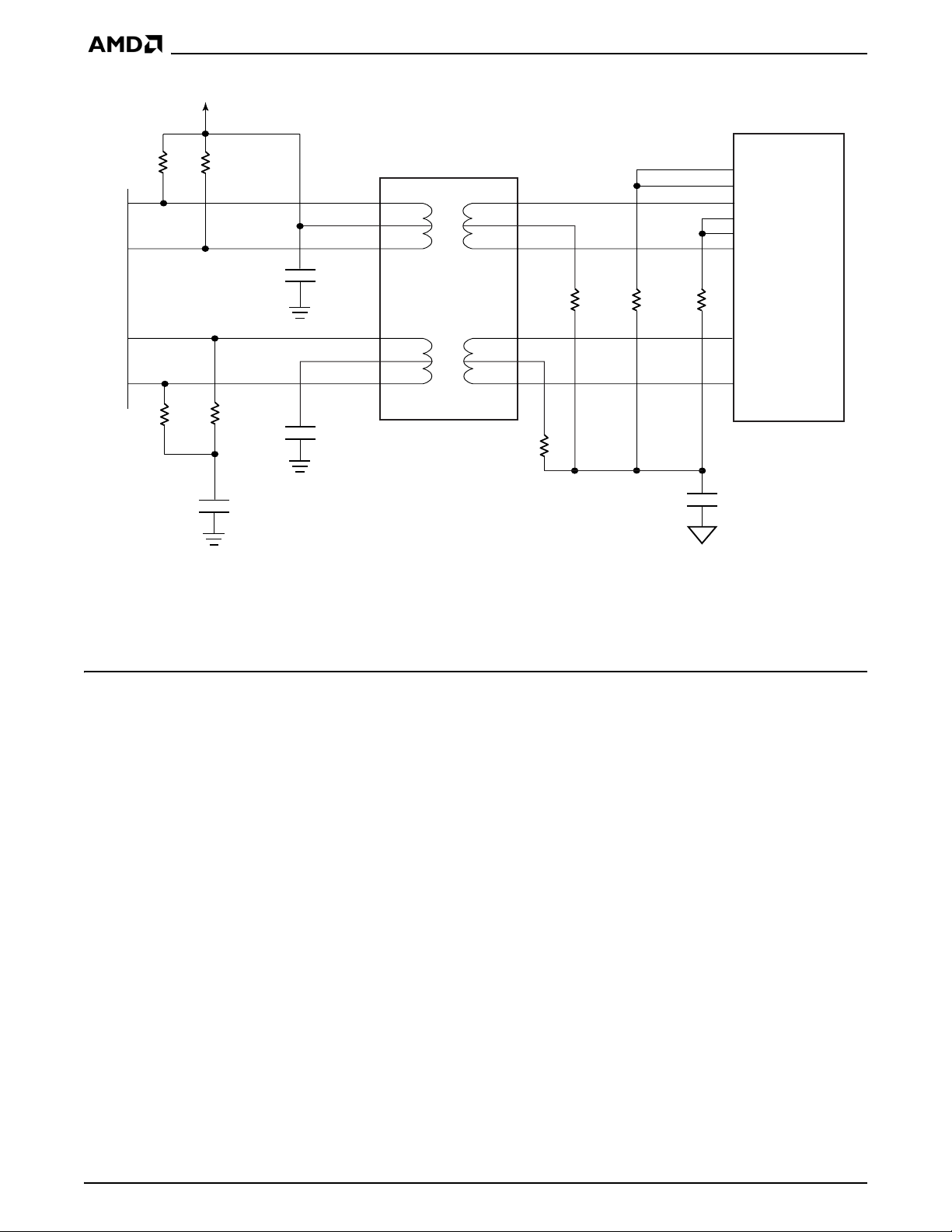
(Note 1)
TX+
TX-
V
DD
(Note 1)
0.1 μF
DATA SHEET
Isolation
Transformer with
common-mode
chokes
1:1 or 1.25:1
RJ45
Connector
(8)
(7)
TX+ (1)
(5)
(4)
TX- (2)
75 Ω75Ω75 Ω
RX+
RX-
(Note 2) (Note 2)
Notes:
1. 49.9 Ω if a 1:1 isolation transformer is used or 78.1 Ω if a 1.25:1 isolation transformer is used.
2. 49.9 Ω is normal, but 54.9 Ω can be used for extended cable length operation.
0.1 μF
0.1 μF
1:1
Figure 3. TX± and RX± Termination for 100BASE-TX and 10BASE-T
Clock/Data Recovery
The equalized MLT-3 signal passes through a slicer circuit which then converts it to NRZI format. The NetPHY-1LP device uses an analog phase-locked loop
(APLL) to extract clock information from the incoming
NRZI data. The extracted clock is used to re-time the
data stream and set the data boundaries. The transmit
clock is locked to the 25-MHz clock input, while the receive clock is locked to the incoming data streams.
When initial lock is achieved, the APLL switches to lock
to the data stream, extracts a 125 MHz clock from it
and use that for bit framing to recover data. The recovered 125 MHz clock is also used to generate the 25
MHz RX_CLK. The APLL requires no external components for its operation and has high noise immunity and
low jitter. It provides fast phase align (lock) to data in
one transition and its data/clock acquisition time after
power-on is less than 60 transitions.
The APLL can maintain lock on run-lengths of up to 60
data bits in the absence of signal transitions. When no
valid data is present, i.e., when the SD is de-asserted,
the APLL switches back to lock with TX_CLK, thus providing a continuously running RX_CLK.
RX+ (3)
RX- (6)
75Ω
470 pF, 2 kV
(chassis ground)
22236G-5
The recovered data is converted from NRZI-to-NRZ
and then to a 5-bit parallel format. The 5-bit parallel
data is not necessarily aligned to 4B/5B code-group’s
symbol boundary. The data is presented to PCS at receive data register output, gated by the 25-MHz
RX_CLK.
PLL Clock Synthesizer
The NetPHY-1LP device includes an on-chip PLL clock
synthesizer that generates a 125 MHz and a 25 MHz
clock for the 100BASE-TX or a 100 MHz and 20 MHz
clock for the 10BASE-T and Auto-Negotiation operations. Only one external 25 MHz crystal or a signal
source is required as a reference clock.
After power-on or reset, the PLL clock synthesizer is
defaulted to generating the 20 MHz clock output and
will stay active until the 100BASE-X operation mode is
selected.
Clock and Crystal Inputs
A 25 MHz crystal can be used for XTL± inputs to the
NetPHY-1LP. The crystal should be parallel resonant
and have a frequency stability of ±100 ppm and a frequency tolerance ±50 ppm. Recommended parts are
22 Am79C874 22235K
Page 23
DATA SHEET
Ecliptek (EC-AT-25.000M, ECSM-AT-25.000M) and
Epson (MA-505-25.000M).
Alternatively, a crystal oscillator can be used to source
a clock on the REFCLK input. The oscillator must be 25
MHz ±50 ppm with a 40% to 60% duty cycle. Recommended parts are Ecliptek (EC1300 HSTS-25.000M)
and Epson (MA506-25.000 MHz).
Note that PLL oscillators cannot be used for XTL± or
REFCLK.
Using crystals or oscillators beyond these specifications will not guarantee successful operation of the
NetPHY-1LP.
10BASE-T Block
The NetPHY-1LP transceiver incorporates the
10BASE-T physical layer functions, including clock recovery (ENDEC), MAUs, and transceiver functions.
The NetPHY-1LP transceiver receives 10-Mbps data
from the MAC, switch, or repeater across the MII at 2.5
million nibbles per second (parallel), or 10 million bits
per second (serial). It then Manchester encodes the
data before transmission to the network.
Refer to Figure 4 for the 10BASE-T transmit and receive data paths.
Clock Data
Manchester
Encoder
Clock Data
Manchester
Decoder
10BASE-T medium requires use of the integrated
10BASE-T MAU and uses the differential driver circuitry on the TX± pins.
TX± is a differential twisted-pair driver. When properly
terminated, TX± meets the transmitter electrical requirements for 10BASE-T transmitters as specified in
IEEE 802.3, Section 14.3.1.2. The load is a twisted pair
cable that meets IEEE 802.3, Section 14.4.
The TX± signal is filtered on the chip to reduce harmonic content per Section 14.3.2.1 (10BASE-T). Since
filtering is performed in silicon, TX± can be connected
directly to a standard transformer. External filtering
modules are not needed
Twisted Pair Receive Process
In 10BASE-T mode, the signal first passes through a
third order Elliptical filter, which filters all the noise from
the cable, board, and transformer. This eliminates the
need for a 10BASE-T external filter. A Manchester decoder and a Serial-to-Parallel converter then follow to
generate the 4-bit nibble in MII mode.
RX+
ports are differential twisted-pair receivers. When
properly terminated, each RX+
port meets the electrical
requirements for 10BASE-T receivers as specified in
IEEE 802.3, Section 14.3.1.3. Each receiver has internal filtering and does not require external filter modules
or common mode chokes.
Signals appearing at the RX± differential input pair are
routed to the internal decoder. The receiver function
meets the propagation delays and jitter requirements
specified by the 10BASE-T standard. The receiver
squelch level drops to half its threshold value after unsquelch to allow reception of minimum amplitude signals and to mitigate carrier fade in the event of worst
case signal attenuation and crosstalk noise conditions.
Twisted Pair Interface Status
The NetPHY-1LP transceiver will power up in the Link
Fail state. The Auto-Negotiation algorithm will apply to
allow it to enter the Link Pass state. A link-pulse detection circuit constantly monitors the RX± pins for the
Loopback
(Register 0)
Squelch
Circuit
presence of valid link pulses. In the Link Pass state, re-
TX Driver
RX Driver
ceive activity which passes the pulse width/amplitude
requirements of the RX± inputs cause the PCS Control
block to assert Carrier Sense (CRS) signal at the MII interface.
RX±TX±
Figure 4. 10BASE-T Transmit /Receive Data Paths
22236G-6
Collision Detect Function
Simultaneous activity (presence of valid data signals)
from both the internal encoder transmit function and
Twisted Pair Transmit Process
In 10BASE-T mode, Manchester code will be generated by the 10BASE-T core logic, which will then be
synthesized through the output waveshaping driver.
This will help reduce any EMI emission, eliminating the
need for an external filter. Data transmission over the
the twisted pair RX± pins constitutes a collision,
thereby causing the PCS Control block to assert the
COL pin at the MII.
Collisions cause the PCS Control block to assert the
Carrier Sense (CRS) and Collision (COL) signals at the
MII. In the Link Fail state, this block would cause the
22235K Am79C874 23
Page 24

DATA SHEET
PCS Control block to de-assert Carrier Sense (CRS)
and Collision (COL).
Jabber Function
The Jabber function inhibits the 10BASE-T twisted pair
transmit function of the NetPHY-1LP transceiver device
if the TX± circuits are active for an excessive period
(20-150 ms). This prevents one port from disrupting the
network due to a stuck-on or faulty transmitter condition. If the maximum transmit time is exceeded, the
data path through the 10BASE-T transmitter circuitry is
disabled (although Link Test pulses will continue to be
sent). The PCS Control block also asserts the COL pin
at the MII and sets the Jabber Detect bit in MII Register
1. Once the internal transmit data stream from the
MENDEC stops, an unjab time of 250-750 ms will
elapse before this block causes the PCS Control block
to de-assert the COL indication and re-enable the
transmit circuitry.
When jabber is detected, this block causes the PCS
control block to assert the COL pin and allows the PCS
Control block to assert or de-assert the CRS pin to indicate the current state of the RX± pair. If there is no receive activity on RX±, this block causes the PCS
Control block to assert only the COL pin at the MII. If
there is RX± activity, this block causes the PCS Control
block to assert both COL and CRS at the MII. The Jabber function can be disabled by setting MII Register 21,
bit 12.
Reverse Polarity Detection and Correction
Proper 10BASE-T receiver operation requires that the
differential input signal be the correct polarity. That is,
the RX+ line is connected to the RX+ input pin, and the
RX- line is connected to the RX- input pin. Improper
setup of the external wiring can cause the polarity to be
reversed. The NetPHY-1LP receiver has the ability to
detect the polarity of the incoming signal and compensate for it. Thus, the proper signal will appear on the
MDI regardless of the polarity of the input signals.
The internal polarity detection and correction circuitry is
set during the reception of the normal link pulses (NLP)
or packets. The receiver detects the polarity of the input
signal on the first NLP. It locks the polarity correction
circuitry after the reception of two consecutive packets.
The state of the polarity correction circuitry is locked as
long as link is established.
Auto-Negotiation and Miscellaneous Functions
Auto-Negotiation
The NetPHY-1LP device has the ability to negotiate its
mode of operation over the twisted pair using the AutoNegotiation mechanism defined in Clause 28 of the
IEEE 802.3u specification. Auto-Negotiation may be
enabled or disabled by hardware (ANEGA, pin 56) or
software (MII Register 0, bit 12) control (see Table ).
The NetPHY-1LP device will automatically choose its
mode of operation by advertising its abilities and comparing them with those received from its link partner
whenever Auto-Negotiation is enabled. Note that AutoNegotiation is not supported in 100BASE-FX mode.
The content of MII Register 4 is sent to the link partner
during Auto-Negotiation, coded in Fast Link Pulses
(FLPs). MII Register 4, bits 8:5 reflect the state of the
TECH_SEL[2:0] pins after reset.
After reset, software can change any of these bits from
1 to 0 and back to 1, but not from 0 to 1 via the management interface. Therefore, hardware settings have
priority over software. A write to Register 4 does not
cause the device to restart Auto-Negotiation.
When Auto-Negotiation is enabled, the NetPHY-1LP
device sends FLP during the one of the following conditions: (a) power on, (b) link loss, or (c) restart command. At the same time, the device monitors incoming
data to determine its mode of operation. When the device receives a burst of FLPs from its link partner with
three identical link code words (ignoring acknowledge
bit), it stores these code words in MII Register 5 and
waits for the next three identical code words. Once the
device detects the second code word, it will configure
itself to the highest technology that is common to both
ends. The technology priorities are: (1) 100BASE-TX,
full-duplex, (2) 100BASE-TX, half-duplex, (3) 10BASET, full-duplex, and (4) 10BASE-T half-duplex.
Parallel Detection
The parallel detection circuit is enabled as soon as either 10BASE-T idle or 100BASE-TX idle is detected.
The mode of operation gets configured based on the
technology of the incoming signal. The NetPHY-1LP
device can also check for a 10BASE-T NLP or
100BASE-TX idle symbol. If either is detected, the device automatically configures to match the detected operating speed in half-duplex mode. This ability allows
the device to communicate with legacy 10BASE-T and
100BASE-TX systems.
24 Am79C874 22235K
Page 25

DATA SHEET
Table 6. Speed and Duplex Capabilities
ANEGA Tech[2] Tech[1] Tech[0] Speed Duplex ANEG-EN
Capabilities/ANEG(Hardwired on Board) (Changeable in MII Register 0)
0000 Yes
0 0 0 1 No No No 10HD
0 0 1 0 No No No 100HD
0 0 1 1 No No No 100HD
0100 Yes
0 1 0 1 No No No 10FD
0 1 1 0 No No No 100FD
0 1 1 1 No No No 100FD
1000 Yes
1001 Yes
1010 Yes
1011 Yes
1100 Yes
1101 Yes
1110 Yes
1111 Yes
1
1
2
Yes2 Yes
2
Yes2 Yes
2
Yes2 Yes
2
Yes2 Yes
2
Yes2 Yes
2
Yes2 Yes
2
Yes2 Yes
3
1
Yes
1
Yes
Yes2 Yes
No All Capabilities
No All Capabilities
3
3
3
3
3
3
3
3
No Capabilities, ANEG
100HD, 10HD, ANEG
No Capabilities, ANEG
10FD/HD, ANEG
100FD/HD, ANEG
All Capabilities, ANEG
10HD, ANEG
100HD, ANEG
1. MII Register 0 (speed and duplex bits) must be set by the MAC to achieve a link.
2. When Auto-Negotiation is enabled, these bits can be written but will be ignored by the PHY.
3. The advertised abilities in MII Register 4 cannot exceed the abilities of MII Register 1. Auto-Negotiation should always
remain enabled. Hardware settings override software settings in registers.
Far-End Fault
Auto-Negotiation provides a remote fault capability for
detecting asymmetric link failure. Since 100Base-FX
systems do not use Auto-Negotiation, an alternative,
in-band signaling scheme, Far-End Fault is used to signal remote fault conditions. Far-End Fault is a stream
of 63 consecutive 1s followed by one logic 0. This pattern is repeated three times. A Far-End Fault will be
signaled under three conditions: (1) when no activity is
received from the link partner, (2) when the clock recovery circuit detects signal error or PLL lock error, and (3)
when the management entity sets the transmit FEF bit
(MII Register 21, bit 7).
The Far-End Fault mechanism defaults to enable
100BASE-FX mode and disable 100BASE-TX and
10BASE-T modes, and may be controlled by software
after reset.
SQE (Heartbeat)
When the SQE test is enabled, a COL signal with a 515 bit time pulse will be issued after each transmitting
packet. SQE is enabled and disabled via MII Register
16, bit 11.
Register 0, bit 14 (Loopback) or MII Register 21, bit 3
(EN_RPBK).
The local loopback routes transmitted data at the output of NRZ-to-NRZI conversion module back to the
receiving path’s clock and data recovery module for
connection to PCS in 5 bits symbol format. This loopback is used to check all the connections at the 5-bit
symbol bus side and the operation of analog phase
locked loop. In local loopback, the SD output is forced
to logic one and TX± outputs are tristated.
During local loopback, a 10-Mbps link is sent to the link
partner. In either 100BASE-TX or 10BASE-T loopback
mode, the link for 10 Mbps is forced (Register 21, bit
14) and is seen externally. If packets are transmitted
from the Device Under Test (DUT), the link between the
DUT and link partner is lost. Ceasing transmission
causes the link to go back up.
In order to perform a local loopback, one of the folllowing procedures must be performed:
1. If ANEGA is already on, establish a link with a partner, and then enable bit 14 looback, or
2. If ANEGA is low/off, enable loopback bit 14.
Loopback Operation
A local loopback and remote loopback are provided for
testing. They can be enabled by writing to either MII
In remote loopback, incoming data passes through the
equalizer and clock recovery, then loop back to NRZI/
MLT3 conversion module and out to the driver. This
22235K Am79C874 25
Page 26

DATA SHEET
loopback is used to check the device’s connection on
the media side and the operation of its internal adaptive
equalizer, phase-locked loop, and digital wave shape
synthesizer. During remote loopback, signal detect
(SD) output is forced to logic zero. Note that remote
loopback operates only in 100BASE-TX mode.
External loopback can be accomplished using an external loopback cable with TX± connected to RX±. External loopback works for both 10 Mbps and 100 Mbps
after setting Register 0, bit 8 to force full duplex and bit
13 to set the speed.
Reset
The NetPHY-1LP device can be reset in the three following ways:
1. During initial power on (with internal power on reset
circuit).
2. At hardware reset. A logic low signal of no less than
155 µs pulse width applied to the RST
pin.
3. At software reset. Write a 1 to MII Register 0, bit 15.
LED Port Configuration
The NetPHY-1LP device has several pins that are used
for both device configuration and LED drivers. These
pins set the configuration of the device on the rising
edge of RST
spective port. See Table for standard LED selections
and Table 5 for advanced LED selections.
The polarity of the LED drivers (Active-LOW or ActiveHIGH) is set at the rising edge of RST
at the rising edge of RST
and thereafter indicate the state of the re-
. If the pin is LOW
, it becomes an active-HIGH
driver. If it is HIGH at the rising edge of RST
, it becomes
an active-LOW driver.
Proper configuration requires pull-up or pull-down resistors. As shown in the Pin Description sections, each
of the LED/Configuration pins has internal pull-up resistors. If the pin’s LED functionality is not used, the pin
may still need to be terminated via an external pulldown resistor according to the desired configuration.
The resistor value is not critical and can be in the range
of 1 kΩ to 1 0 kΩ. Otherwise, a terminating resistor must
be used with the LED. Suggested LED connection diagrams simplifying the board design are shown in Figure
5 (standard) and Figure 6 (advanced).
The value of the series resistor (R
to ensure sufficient illumination of the LED. R
) should be selected
L
is de-
L
pendent on the rating of the LED.
The LED pins are totem-pole configuration and should
not be tied together.
Table 7. Standard LED Mode and Advanced LED
Mode Pins
Mode Standard LED Pin Advanced LED Pin
10 Mbps LEDSPD[1] LEDBTA/LEDBTB
100 Mbps LEDSPD[0] LEDTXA/LEDTXB
Link LEDLNK LEDLNK
Duplex LEDDPX see Table 8
Tx Activity LEDTX not available
Rx Activity LEDRX see Table 9
26 Am79C874 22235K
Page 27

DATA SHEET
100 Mbps LEDSPD[0]
10 Mbps LEDSP[1]
Collision LEDCOL
Duplex LEDDPX
Transmit LEDTX
Receive LEDRX
Link (Note 1) LEDLNK
LED
LED
LED
LED
LED
LED
VCC
330
VCCLED
330
VCC
330
VCC
330
VCC
330
VCC
330
VCC
330
Link (Note 2) LEDLNK
Notes:
1. Use for non 7-wire interface configurations.
2. Use for 7-wire interface configurations.
Figure 5. Standard LED Configuration
Table 8. Duplex LED Status Configuration in Advanced LED Mode
Mode Pin LED Status
10 Mbps Half Duplex LEDBTA (pin 44) ON
10 Mbps Full Duplex LEDBTB (pin 47) ON
100 Mbps Half Duplex LEDTXA (pin 57) ON
100 Mbps Full Duplex LEDTXB (pin 58) ON
1. Assumes configuration as in Figure 6.
2. Duplex LEDs are solid colors when there is no transmit or receive activity.
LED
330
22236G-7
1
2
22235K Am79C874 27
Page 28
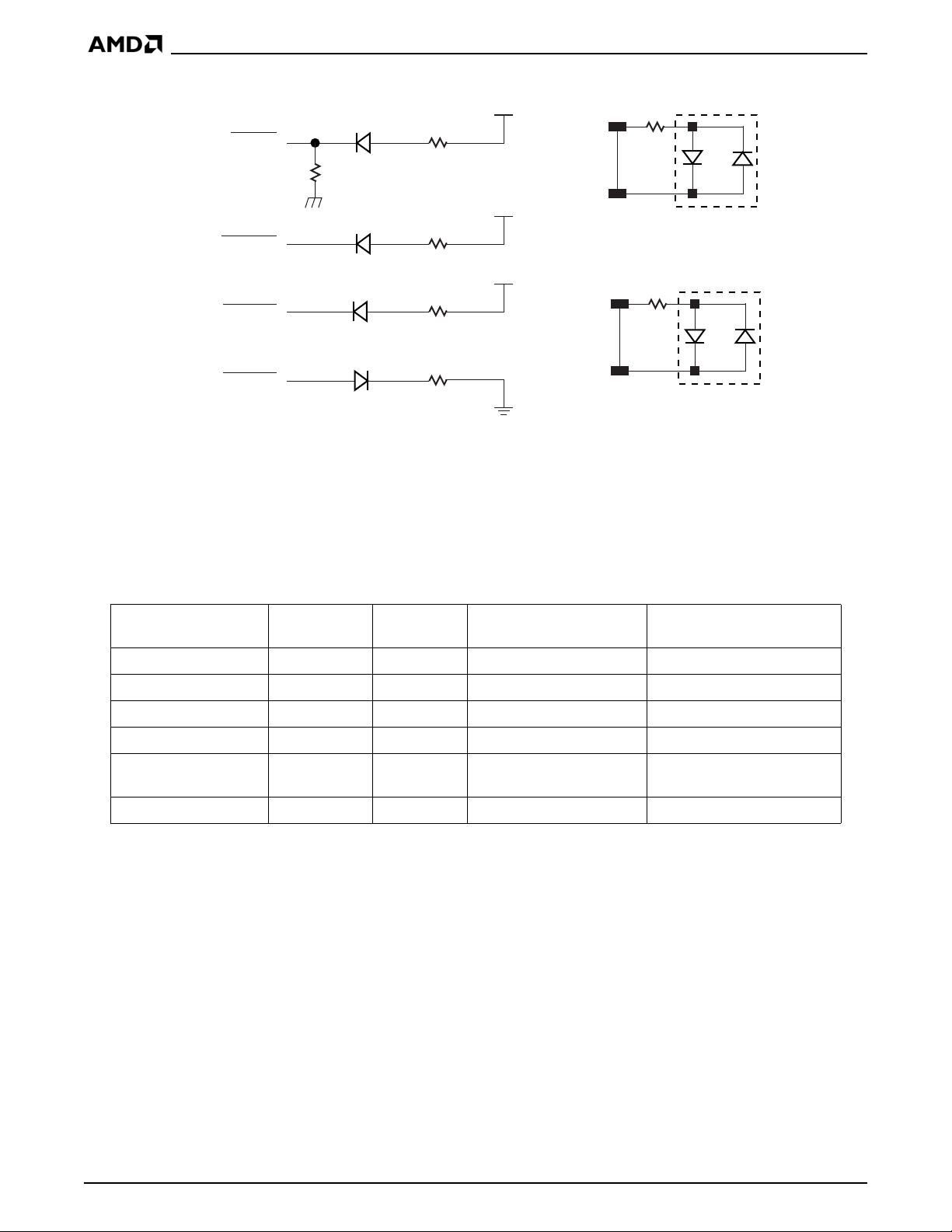
DATA SHEET
VCC
LED
Receive LEDRX
5 K
LED
Collision LEDCOL
LED
Link (Note 1) LEDLNK
LED
Link (Note 2) LEDLNK
Notes:
1. Use for non 7-wire interface configurations.
2. Use for 7-wire interface configurations.
3. Refer to Table 7, Table 8 and Table 9 for Mode, Duplex and Activity functions.
330
330
330
330
LEDBTA
LEDBTB
VCC
VCC
LEDTXA
LEDTXB
100BASE-TX LED Indicator
Figure 6. Advanced LED Configuration
300
Dual-Color
LED
10BASE-T LED Indicator
300
Dual-Color
LED
22236G-8
Table 9. Activity LED Configuration in Advanced LED Mode
CONF_ALED
Mode
10 Mbps Half Duplex 0 0 LEDBTA/LEDBTB Blinks on Tx and Rx activity
10 Mbps Half Duplex 1 0 LEDBTA/LEDBTB Blinks on Rx activity only
100 Mbps Half Duplex 0 0 LEDTXA/LEDTXB Blinks on Tx and Rx activity
100 Mbps Half Duplex 1 0 LEDTXA/LEDTXB Blinks on Rx activity only
Full Duplex X 0
Any X 1 LEDTX, LEDRX Blinks on respective pins
1. Assumes configuration as in Figure 6.
2. The LED will not blink for the duration of a packet if the transmit and receive activity are simultaneously active ( i.e.,
in opposite phase).
Reg 21, bit 10
Power Savings Mechanisms
The power consumption of the device is significantly
reduced by its built-in power down features. Separate
power supply lines are also used to power the
10BASE-T circuitry and the 100BASE-TX circuitry.
Therefore, the two modes of operation can be turnedon and turned-off independently. Whenever the NetPHY-1LP device is set to operate in a 100BASE-TX
mode, the 10BASE-T circuitry is powered down, and
when in 10BASE-T mode, the 100BASE-TX circuitry is
powered down.
LED_SEL
Reg 21, bit 9 Pin LED Status
LEDBTA/LEDBTB or
LEDTXA/LEDTXB
The NetPHY-1LP device offers the following power
management: Selectable Transformer, Power Down,
Unplugged, and Idle.
Selectable Transformer
The TX outputs can drive either a 1:1 transformer or a
1.25:1 transformer. The latter can be used to reduce
transmit power further. The current at the TX± pins for
a 1:1 ratio transformer is 40 mA for MLT-3 and 100 mA
for 10BASE-T. Using the 1.25:1 ratio reduces the current to 30 mA for MLT-3 and 67 mA for 10BASE-T.
1
Blinks on Rx activity only
The cost of using the 1.25:1 option is in impedance
coupling. The reflected capacitance is increased by the
2
28 Am79C874 22235K
Page 29

DATA SHEET
square of the ratio (1.252 = 1.56). Thus, the reflected
capacitance on the media side is roughly one and a half
times the capacitance on the board. Extra care in the
layout to control capacitance on the board is required.
Power Down
Most of the NetPHY-1LP device can be disabled via the
Power Down bit in MII Register 0, bit 11. Setting this bit
will power down the entire device with the exception of
the MDIO/MDC management circuitry.
Unplugged
The TX output driver limits the drive capability if the receiver does not detect a link partner within 4 seconds.
This prevents “wasted” power. If the receiver detects
the absence of a link partner, the transmitter is limited
to transmitting normal link pulses. Any energy detected
by the receiver enables full transmit and receive capabilities. The power savings is most notable when the
port is unconnected. Typical power drops to one third
of normal.
Idle Wire
This can be achieved by writing to MII Register 16, bit
0. During this mode, if there is no data other than idles
coming in, the receive clock (RX_CLK) will turn off to
save power for the attached controller. RX_CLK will resume operation one clock period prior to the assertion
of RX_DV. The receive clock will again shut off 64 clock
cycles after RX_DV gets deasserted. Typical power
savings of 100 mW can be realized in some MACs.
22235K Am79C874 29
Page 30
DATA SHEET
PHY CONTROL AND MANAGEMENT BLOCK (PCM BLOCK)
agement Data Clock (MDC). A station management
entity which is attached to multiple PHY entities must
have prior knowledge of the appropriate PHY address
Register Administration for 100BASE-X PHY Device
The management interface specified in Clause 22 of
the IEEE 802.3u standard provides for a simple two
wire, serial interface to connect a management entity
and a managed PHY for the purpose of controlling the
PHY and gathering status information. The two lines
are Management Data Input/Output (MDIO), and Man-
for each PHY entity.
Description of the Methodology
The management interface physically transports management information across the MII. The information is
encapsulated in a frame format as specified in Clause
22 of IEEE 802.3u draft standard and is shown in
Tab le .
Table 10. Clause 22 Management Frame Format
PRE ST OP PHYAD REGADD TA DATA IDLE
READ 1.1 01 10 AAAAA RRRRR Z0 D...........D Z
WRITE 1.1 01 01 AAAAA RRRRR 10 D...........D Z
The PHYAD field, which is five bits wide, allows 32
unique PHY addresses. The managed PHY layer device that is connected to a station management entity
via the MII interface has to respond to transactions
entity attached to multiple PHYs, such as in a managed
802.3 Repeater or Ethernet switch, is required to have
prior knowledge of the appropriate PHY address. See
Table and Figure 7.
addressed to the PHY address. A station management
Table 11. PHY Address Setting Frame Structure
PRE ST OP PHYAD REGADD TA DATA IDLE
READ 1.1 01 10 00000 RRRRR Z0 XXXXXXXXXPPAAAAA Z
WRITE 1.1 01 01 00000 RRRRR 10 XXXXXXXXXPPAAAAA Z
MDC
MDIO
z
(STA)
MDIO
(PHY)
MDC
MDIO
z
(STA)
Idle Start Opcode
z
z
z
01101011000001 0 0110000 010000010
Idle Start Opcode
z
(Read)
010110110000 0010011000 1000000000
(Write)
PHY Address
16h, Port 2
PHY Address
16h, Port 2
Register Address
MII Status, 1h
Register Address
MII Control, 0h
z
TA
Read Operation
TA
Write Operation
Figure 7. PHY Management Read and Write Operations
z
z
Register Data Idle
z
z
Register Data Idle
22236G-9
30 Am79C874 22235K
Page 31

DATA SHEET
Bad Management Frame Handling
The management block of the device can recognize
management frames without preambles (preamble
suppression). However, if it receives a bad management frame, it will go into a Bad Management Frame
state. It will stay in this state and will not respond to any
management frame without preambles until a frame
with a full 32-bit preamble is received, then it will return
to normal operation.
A bad management frame is a frame that does not
comply with the IEEE standard specification. It can be
one with less than 32-bit preamble, with illegal OP field,
etc. However, a frame with more than 32 preamble bits
is considered to be a good frame.
After a reset, the NetPHY-1LP device requires a minimum preamble of 32 bits before management data
(MDIO) can be received. After that, the management
data being received by the NetPHY-1LP device does
not require a preamble.
REGISTER DESCRIPTIONS
The following table lists the supported registers (register addresses are in decimal).
Table 12. Supported Registers
Register
Address Description
0 MII Management Control Register
1 MII Management Status Register
2 PHY Identifier 1 Register
3 PHY Identifier 2 Register
4 Auto-Negotiation Advertisement Register
5 Auto-Negotiation Link Partner Ability Register
6 Auto-Negotiation Expansion Register
7 Next Page Advertisement Register
8-15 Reserved
16 Miscellaneous Features Register
17 Interrupt Control/Status Register
18 Diagnostic Register
19 Power Management & Loopback Register
20 Reserved
21 Mode Control Register
22 Reserved
23 Disconnect Counter
24 Receive Error Counter
25-31 Reserved
The Physical Address of the PHY is set using the pins
defined as PHYAD[4:0]. These input signals are
strapped externally and sampled as when reset goes
high. The PHYAD pins can be reprogrammed via software.
Serial Management Registers
A detailed definition of each Serial Management register is provided in the following table.
Table 13. Serial Management Registers
Type Des c r i p t i on
RW Readable and writable
SC Self Clearing
LL Latch Low until clear
RO Read Only
RC Cleared on the read operation
LH Latch high until clear
22235K Am79C874 31
Page 32

Table 14. MII Management Control Register (Register 0)
Reg Bit Name Description
1 = PHY reset.
0 15 Reset
0 14 Loopback
0 = Normal operation.
This bit is self-clearing. This Reset will require a minimum of 1 ms,
or is complete when the register clears.
1 = Enable loopback mode. This will loopback TXD to RXD, thus it
will ignore all the activity on the cable media. During loopback, a
10-Mbps link is sent to the link partner (Register 21, bit 14 is forced.)
0 = Disable Loopback mode. Normal operation.
DATA SHEET
Read/
Write Default
RW/SC 0
RW 0
1 = 100 Mbps, 0 = 10 Mbps. This bit will be ignored if Auto
0 13 Speed Select
012
0 11 Power Down
010Isolate
09
0 8 Duplex Mode
0 7 Collision Test
0 6:0 Reserved Write as 0, ignore when read. RW 0
Auto-Neg
Enable
Restart AutoNegotiation
Negotiation is enabled (0.12 = 1).
Refer to Table 3 to determine when this bit can be changed.
1 = Enable auto-negotiate process (overrides 0.13 and 0.8).
0 = Disable auto-negotiate process. Mode selection is controlled via
bit 0.8, 0.13 or through TECH[2:0] pins.
Refer to Table 3 to determine when this bit can be changed.
1 = Power down. The NetPHY-1LP device will shut off all blocks
except for MDIO/MDC interface. Setting PWRDN pin to high will
achieve the same result.
0 = Normal operation.
1 = Electrically isolate the PHY from MII. However, PHY is still able
to respond to MDC/MDIO. The default value of this bit depends on
ISODEF pin, i.e., ISODEF=1, ISO bit will set to 1, & ISODEF=0, ISO
bit will set to 0.
0 = Normal operation.
1 = Restart Auto-Negotiation process.
0 = Normal operation.
1 = Full duplex, 0 = Half duplex.
Refer to Table 3 to determine when this bit can be changed.
1 = Enable collision test, which issues the COL signal in response
to the assertion of TX_EN signal. Collision test is disabled if PCSBP
pin is high. Collision test is enabled regardless of the duplex mode.
0 = disable COL test.
RW
RW
RW 0
RW
RW/SC 0
RW
RW 0
Set by
TECH[2:0]
pins
Set by
ANEGA
pin
Set by
ISODEF
pin
Set by
TECH[2:0]
pins
32 Am79C874 22235K
Page 33

DATA SHEET
Table 15. MII Management Status Register (Register 1)
Reg Bit Name Description
1 15 100BASE-T4
1 = 100BASE-T4 able.
0 = Not 100BASE-T4 able.
Read/
Write Default
RO 0
114
113
112
111
1 10:7 Reserved Ignore when read. RO 0
1 6
15
1 4 Remote Fault
100BASE-TX Full
Duplex
100BASE-TX Half
Duplex
10BASE-T Full
Duplex
10BASE-T Half
Duplex
Management
Frame Preamble
Suppression
Auto-Negotiation
Complete
1 = 100BASE-TX Full Duplex.
0 = No 100BASE-TX Full Duplex ability.
1 = 100BASE-TX Half Duplex.
0 = No TX half-duplex ability.
1 = 10BASE-T Full Duplex.
0 = No 10BASE-T Full Duplex ability.
1 = 10BASE-T Half Duplex.
0 = No 10BASE-T ability.
The device accepts management frames that do not have a
preamble after receiving a management frame with a 32-bit or
longer preamble.
1 = Auto-Negotiation process completed. Registers 4, 5, and 6
are valid after this bit is set.
0 = Auto-Negotiation process not completed.
1 = Remote fault condition detected.
0 = No remote fault.
This bit will remain set until it is read via the management
interface.
RO
RO
RO
RO
RO 1
RO 0
RO/LH 0
set by
TECH[2:0]
pins
set by
TECH[2:0]
pins
set by
TECH[2:0]
pins
set by
TECH[2:0]
pins
13
1 2 Link Status
1 1 Jabber Detect
10
Auto-Negotiation
Ability
Extended
Capability
1 = Able to perform Auto-Negotiation function; value is
determined by ANEGA pin.
0 = Unable to perform Auto-Negotiation function.
1 = Link is established; however, if the NetPHY-1LP device link
fails, this bit will be cleared and remain cleared until Register 1
is read via management interface.
0 = link is down.
1 = Jabber condition detected.
0 = No Jabber condition detected.
1 = Extended register capable. This bit is tied permanently to
one.
Table 16. PHY Identifier 1 Register (Register 2)
Reg Name Description
215:0OUI
Composed of the 3rd through 18th bits of the Organizationally
Unique Identifier (OUI), respectively.
RO
RO/LL 0
RO/LH 0
RO 1
Read/
Write Default
RO 0022(H)
set by
ANEGA pin
22235K Am79C874 33
Page 34

DATA SHEET
Table 17. PHY Identifier 2 Register (Register 3)
Read/
Reg Bit Name Description
3 15:10 OUI Assigned to the 19th through 24th bits of the OUI. RO 010101
3 9:4 Model Number Six-bit manufacturer’s model number. RO 100001
3 3:0 Revision Number Four-bit manufacturer’s revision number. RO 1011
Write Default
Table 18. Auto-Negotiation Advertisement Register (Register 4)
Read/
Reg Bit Name Description
4 15 Next Page
4 14 Acknowledge
1 = Next Page enabled.
0 = Next Page disabled.
This bit will be set internally after receiving three consecutive
and consistent FLP bursts.
Write Default
RW 0
RO 0
4 13 Remote Fault
4 12:11 Reserved For future technology. RW 0
410FDFC
4 9 100BASE-T4
48
47
46
45
4 4:0 Selector Field [00001] = IEEE 802.3. RO 00001
100BASE-TX
Full Duplex
100BASE-TX
Half Duplex
10BASE-T
Full Duplex
10BASE-T
Half Duplex
1 = Remote fault supported.
0 = No remote fault.
Full Duplex Flow Control:
1 = Advertise that the DTE(MAC) has implemented both the
optional MAC control sublayer and the pause function as
specified in clause 31 and annex 31 B of 802.3u.
0 = No MAC-based full duplex flow control.
NetPHY-1LP device does not support 100BASE-T4 function,
i.e., this bit ties to zero.
1 = 100BASE-TX Full Duplex.
0 = No 100BASE-TX Full Duplex ability.
Default is set by Register 1.14.
1 = 100BASE-TX Half Duplex.
0 = No 100BASE-TX Half Duplex capability.
Default is set by Register 1.13
1 = 10 Mbps Full Duplex.
0 = No 10 Mbps Full Duplex capability.
Default is set by Register 1.12.
1 = 10 Mbps Half Duplex.
0 = No 10 Mbps Half Duplex capability
Default is set by Register 1.11.
RW 0
RW 0
RO 0
set by
RW
RW
RW
RW
TECH [2:0]
pins
set by
TECH[2:0]
pins
set by
TECH[2:0]
pins
set by
TECH[2:0]
pins
34 Am79C874 22235K
Page 35

DATA SHEET
Table 19. Auto-Negotiation Link Partner Ability Register in Base Page Format (Register 5)
Read/
Reg Bit Name Description
Write Default
5 15 Next Page
5 14 Acknowledge
5 13 Remote Fault
5 12:11 Reserved Reserved for Future Technology RO
5 10 Flow Control
5 9 100BASE-T4
58
57
56
55
5 4:0 Selector Field Link Partner Selector Field RO 00001
100BASE-TX Full
Duplex
100BASE-TX Half
Duplex
10BASE-T Full
Duplex
10BASE-T Half
Duplex
1 = Next Page Requested by Link Partner
0 = Next Page Not Requested
1 = Link Partner Acknowledgement
0 = No Link Partner Acknowledgement
1 = Link Partner Remote Fault Request
0 = No Link Partner Remote Fault Request
1 = Link Partner supports Flow Control.
0 = Link Partner does not support Flow Control.
1 = Remote Partner is 100BASE-T4 Capable
0 = Remote Partner is not 100BASE-T4 Capable
1 = Link Partner is capable of 100BASE-TX Full Duplex
0 = Link Partner is Not Capable of 100BASE-TX Full
Duplex
1 = Link Partner is Capable of 100BASE-TX Half
Duplex
0 = Link Partner is Not Capable of 100BASE-TX Half
Duplex
1 = Link Partner is capable of 10BASE-T Full Duplex
0 = Link Partner is Not Capable of 10BASE-T Full
Duplex
1 = Link Partner is capable of 10BASE-T Half Duplex
0 = Link Partner is Not Capable of 10BASE-T Half
Duplex
RO 0
RO 0
RO 0
RO 0
RO 0
RO 0
RO 0
RO 0
RO 0
Table 20. Auto-Negotiation LInk Partner Ability Register in Next Page Format (Register 5)
Read/
Reg Bit Name Description
5 15 Next Page
5 14 Acknowledge
5 13 Message Page
5 12 Acknowledge 2
5 11 Toggle Link Partner Toggle RO 0
5 10:0 Message Field Link Partner’s Message Code RO 0
1 = Next Page Requested by Link Partner
0 = Next Page Not Requested
1 = Link Partner Acknowledgement
0 = No Link Partner Acknowledgement
1 = Link Partner message Page Request
0 = No Link partner Message Page Request
1 = Link Partner can Comply Next Page Request
0 = Link Partner cannot Comply Next Page Request
Write Default
RO 0
RO 0
RO 0
RO 0
22235K Am79C874 35
Page 36

DATA SHEET
Table 21. Auto-Negotiation Expansion Register (Register 6)
Read/
Reg Bit Name Description
6 15:5 Reserved Ignore when read. RO 0
1 = Fault detected by parallel detection logic. This fault is due to
64
Parallel Detection
Fault
more than one technology detecting concurrent link up
conditions. This bit is cleared upon reading this register.
0 = No fault detected by parallel detection logic.
Write Default
RO/LH 0
63
6 2 Next Page Able Next page is supported. This bit is permanently tied to 1. RO 1
6 1 Page Received
60
Link Partner Next
Page Able
Link Partner AutoNegotiation Able
1 = Link partner supports next page function.
0 = Link partner does not support next page function.
This bit is set when a new link code word has been received into
the Auto-Negotiation Link Partner Ability Register. This bit is
cleared upon reading this register.
1 = Link partner is auto-negotiation able.
0 = Link partner is not auto-negotiation able.
RO 0
RO/LH 0
RO 0
Table 22. Auto-Negotiation Next Page Advertisement Register (Register 7)
Read/
Reg Bit Name Description
Next page indication:
715NP
7 14 Reserved Ignore when read. RO 0
713MP
712ACK2
1 = Another Next Page desired.
0 = No other Next Page Transfer desired.
Message page:
1 = Message page.
0 = Un-formatted page.
Acknowledge 2:
1 = Will comply with message.
0 = Cannot comply with message.
Write Default
RW 0
RW 1
RW 0
Toggle:
711TOG_TX
17 10:0 CODE Message/Un-formatted Code Field. RW 001
1 = Previous value of transmitted link code word equals to 0.
0 = Previous value of transmitted link code word equals to 1.
RW 0
Reserved Registers (Registers 8-15, 20, 22, 25-31)
The NetPHY-1LP device contains reserved registers at addresses 8-15, 20, 22, 25-31. These registers should be
ignored when read and should not be written at any time.
36 Am79C874 22235K
Page 37

DATA SHEET
Table 23. Miscellaneous Features Register (Register 16)
Reg Bit Name Description
Read/
Write Default
16 15 Repeater
16 14 INTR_LEVL
16 13:12 Reserved Write as 0, ignore when read. RW 0
16 11 SQE Test Inhibit
16 10
16 9 GPIO_1 Data
16 8 GPIO_1 DIR
16 7 GPIO_0 Data
16 6 GPIO_0 DIR
16 5
16 4 Reverse Polarity
16 3:1 Reserved Write as 0, ignore when read. RO 0
16 0
10BASE-T
Loopback
Auto polarity
Disable
Receive Clock
Control
1= Repeater mode, full-duplex is inactive, and CRS only
responds to receive activity. SQE test function is also disabled.
INTR will be active high if this register bit is set to 1. Pin requires
an external pull-down resistor.
INTR will be active low if this register bit is set to 0. Pin requires
an external pull-up resistor.
1 = Disable 10BASE-T SQE testing.
0 = Enable 10BASE-T SQE testing. A COL pulse is generated
following the completion of a packet transmission.
1 = Enable normal loopback in 10BASE-T mode.
0 = Disable normal loopback in 10BASE-T mode.
When GPIO_1 DIR bit is set to 1, this bit reflects the value of the
GPIO[1] pin. When GPIO_1 DIR bit is set to 0, the value of this bit
will be presented on the GPIO[1] pin.
1 = GPIO[1] pin is an input.
0 = GPIO[1] pin is an output.
When GPIO_0 DIR bit is set to 1, this bit reflects the value of the
GPIO[0] pin. When GPIO[0] DIR bit is set to 0, the value of this bit
will be presented on the GPIO[0] pin.
1 = GPIO[0] pin is an input.
0 = GPIO[0] pin is an output.
1 = Disable auto polarity detection/correction.
0 = Enable auto polarity detection/correction.
When Register 16.5 is set to 0, this bit will be set to 1 if reverse
polarity is detected on the media. Otherwise, it will be 0.
When Register 16.5 is set to 1, writing a 1 to this bit will reverse
the polarity of the transmitter.
Note: Reverse polarity is detected either through eight inverted
NLPs or through a burst of an inverted FLP.
Writing a 1 to this bit will shut off RX_CLK when incoming data is
not present and only if there is LINK present. RX_CLK will resume
activity one clock cycle prior to RX_DV going high, and shut off 64
clock cycles after RX_DV goes low.
A 0 indicates that RX_CLK runs continuously during LINK
whether data is received or not
In loopback and PCS bypass modes, writing to this bit does not
affect RX_CLK. Receive clock will be constantly active.
RW
RW 0
RW 0
RW 0
RW 0
RW 1
RW 0
RW 1
RW 0
RW 0
RW 0
Set by
RPTR
22235K Am79C874 37
Page 38

DATA SHEET
Table 24. Interrupt Control/Status Register (Register 17)
Read/
Reg Bit Name Description
17 15 Jabber_IE Jabber Interrupt Enable RW 0
17 14 Rx_Er_IE Receive Error Interrupt Enable RW 0
17 13 Page_Rx_IE Page Received Interrupt Enable RW 0
17 12 PD_Fault_IE Parallel Detection Fault Interrupt Enable RW 0
17 11 LP_Ack_IE Link Partner Acknowledge Interrupt Enable RW 0
17 10 Link_Not_OK_ IE Link Status Not OK Interrupt Enable RW 0
17 9 R_Fault_IE Remote Fault Interrupt Enable RW 0
17 8 ANeg_Comp_IE Auto-Negotiation Complete Interrupt Enable RW 0
17 7 Jabber_Int This bit is set when a jabber event is detected. RC 0
17 6 Rx_Er_Int This bit is set when RX_ER transitions high. RC 0
17 5 Page_Rx_Int
17 4 PD_Fault_Int This bit is set for a parallel detection fault. RC 0
17 3 LP_Ack_Int
17 2 Link_Not_OK Int
This bit is set when a new page is received from link partner during
Auto-Negotiation.
This bit is set when an FLP with the acknowledge bit set is
received.
This bit is set when link status switches from OK status to Not-OK
(Fail or Ready).
Write Default
RC 0
RC 0
RC 0
17 1 R_Fault_Int This bit is set when a remote fault is detected. RC 0
17 0 A_Neg_Comp Int This bit is set when Auto-Negotiation is complete. RC 0
Table 25. Diagnostic Register (Register 18)
Read/
Reg Bit Name Description
18 15:12 Reserved Ignore when read. RO 0
18 11 DPLX
18 10 Data Rate
18 9 RX_PASS
18 8 RX_LOCK
1 = The result of Auto-Negotiation for Duplex is Full-duplex.
0 = The result of Auto-Negotiation for Duplex is Half-duplex.
1 = The result of Auto-Negotiation for data-rate arbitration is 100
Mbps.
0 = The result of Auto-Negotiation for data-rate arbitration is 10
Mbps.
Operating in 100BASE-X mode:
1 = A valid signal has been received but the PLL has not
necessarily locked.
0 = A valid signal has not been received.
Operating in 10BASE-T mode:
1 = Manchester data has been detected.
0 = Manchester data has not been detected.
1 = Receive PLL has locked onto received signal for selected
data-rate (10BASE-T or 100BASE-X).
0 = Receive PLL has not locked onto received signal.
This bit remains set until it is read.
Write Default
RO 0
RO 0
RO 0
RO/RC 0
18 7:0 Reserved Ignore when read. RO 0
38 Am79C874 22235K
Page 39

DATA SHEET
Table 26. Power/Loopback Register (Register 19)
Read/
Reg Bit Name Description
19 15:7 Reserved RW 00
Transmit transformer ratio selection:
1 = 1.25:1
19 6 TP125
19 5 Low Power Mode
0 = 1:1
The default value of this bit is controlled by reset-read value of pin
20.
1 = Enable advanced power saving mode.
0 = Disable advanced power saving mode
Note: Under normal operating conditions, this mode should never
be disabled. Power dissipation will exceed data sheet values, as
circuitry for both 10 Mbps and 100 Mbps will be turned on.
Write Default
RW 0
RW 1
19 4 Test Loopback
19 3 Digital loopback
19 2 LP_LPBK
19 1
19 0 Reduce Timer
NLP Link Integrity
Te st
1 = Enable test loopback. Data will be transmitted from MII
interface to clock recovery and loopback to MII received data.
1 = Enable loopback.
0 = Normal operation.
1 = Enable link pulse loopback.
0 = Normal operation.
1 = In Auto-Negotiation test mode, send NLP instead of FLP in
order to test NLP receive integrity.
0 = Sending FLP in Auto-Negotiation test mode.
1 = Reduce time constant for Auto-Negotiation timer.
0 = Normal operation.
RW 0
RW 0
RW 0
RW 0
RW 0
22235K Am79C874 39
Page 40

DATA SHEET
Table 27. Mode Control Register (Register 21)
Read/
Reg Bit Name Description
21 15 Reserved RO 0
1 = Force link up without checking NLP. Forced during local
21 14
Force_Link_10
loopback.
0 = Normal Operation.
1 = Ignore link in 100BASE-TX and transmit data. Auto-
21 13
Force_Link_100
Negotiation must be disabled at this time (pin 56 tied low).
0 = Normal Operation.
21 12 Jabber Disable
1 = Disable Jabber function in PHY.
0 = Enable Jabber function in PHY.
1 = Enable 7-wire interface for 10BASE-T operation. This bit is
21 11 7_Wire_Enable
useful only when the chip is not in PCS bypass mode.
0 = Normal operation.
This bit is only applicable to Advanced LED Mode and Duplex
operation.
1 = Activity LED only responds to receive operation.
21 10 CONF_ALED
0 = Activity LED responds to receive and transmit operations for
Half Duplex. LED responds to receive activity in Full Duplex
operation.
This bit should be ignored when Register 0.8 is set to 1.
21 9 LED_SEL
1 = Select NetPHY-1LP device‘s Standard LED configuration.
0 = Use the Advanced LED configuration.
0 = Enable far-end-fault generation and detection function.
21 8 FEF_DISABLE
1 = Disable far-end-fault.
This bit should be ignored when FX mode is disabled.
21 7
Force FEF
Transmit
This bit is set to force to transmit Far End Fault (FEF) pattern. RW 0
Write Default
RW 0
RW 0
RW 0
RW 0
RW 0
RW
RW
LEDRX
LED_SEL
TECH[2:0],
FX_SEL
ANEGA
Set by
/
Set by
,
pins
21 6 RX_ER_CNT Full When Receive Error Counter is full, this bit will be set to 1. RO/ RC 0
21 5
Disable
RX_ER_CNT
21 4 DIS_WDT
21 3 EN_RPBK
21 2 EN_SCRM
21 1 PCSBP
21 0 FX_SEL
1 = Disable Receive Error Counter.
0 = Enable Receive Error Counter.
1 = Disable the watchdog timer in the decipher.
0 = Enable watchdog timer.
1 = Enable remote loopback (MDI loopback for 100BASE-TX).
0 = Disable remote loopback.
1 = Enable data scrambling.
0 = Disable data scrambling.
When FX mode is selected, this bit will be forced to 0.
1 = Bypass PCS.
0 = Enable PC.
1 = FX mode selected.
0 = Disable FX mode.
RW 0
RW 0
RW 0
Set by
RW
RW
RW
SCRAM_EN
Set by
PCSBP pin
Set by
FX_SEL
pin
pin
40 Am79C874 22235K
Page 41

DATA SHEET
Table 28. Disconnect Counter (Register 23)
Reg Bit Name Description
Read/
Write Default
23 15:0
DLOCK drop
counter
Count of PLL lock drop events (100 Mbps operation only) RW 0000
Table 29. Receive Error Counter Register (Register 24)
Read/
Reg Bit Name Description
24 15:0 RX_ER counter Count of receive error events RW 0000
Write Default
22235K Am79C874 41
Page 42

DATA SHEET
ABSOLUTE MAXIMUM RATINGS
Storage Temperature . . . . . . . . . . . . .-55°C to +150°C
Ambient Temperature Under Bias . . . -55°C to +150°C
Supply Voltage. . . . . . . . . . . . . . . . . . -0.5 V to +5.5 V
Voltage Applied to any input pin. . . . . . . -0.5 V to V
Stresses above those listed under Absolute Maximum
Ratings may cause permanent device failure. Functionality at or above these limits is not implied. Exposure to absolute maximum ratings for extended periods
may affect device reliability.
DD
OPERATING RANGES
Commercial (C)
Operating Temperature (TA) . . . . . . . . . 0°C to +70°C
Supply Voltage (All V
) . . . . . . . . . . . . . . +3.3 V ±5%
DD
Industrial (I)
Operating Temperature (TA) . . . . . . . . -40°C to +85°C
Supply Voltage (All V
Operating ranges define those limits between which
functionality of the device is guaranteed.
) . . . . . . . . . . . . . . +3.3 V ±5%
DD
DC CHARACTERISTICS
Note: Parametric values are the same for Commercial and Industrial devices.
Table 30. DC Characteristics
Symbol Parameter Description Test Conditions Minimum Maximum Units
V
V
V
V
V
V
V
IL
IH
OL
OH
OLL
OHL
CMP
Input LOW Voltage 0.8 V
Input HIGH Voltage 2.0 V
Output LOW Voltage IOL = 8 mA 0.4 V
Output HIGH Voltage IOH = -4 mA 2.4 V
Output LOW Voltage (LED) IOL (LED) = 10 mA 0.4 V
Output HIGH Voltage (LED) IOL (LED) = -10 mA VDD –0.4 V
Input Common-Mode Voltage
1
PECL
VDD – 1.5 VDD – 0.7 V
V
IDIFFP
V
OHP
V
OLP
V
SDA
V
SDD
I
IL
I
IH
V
TXOUT
V
TXOS
V
TXR
V
TSQ
V
THS
Differential Input Voltage
1
PECL
VDD = Maximum 400 1,100 mV
Output HIGH Voltage PECL 2PECL Load VDD – 1.025 VDD – 0.60 V
Output LOW Voltage PECL 2PECL Load VDD – 1.81 VDD – 1.62 V
Signal Detect Assertion
Threshold P/P
Signal Detect Deassertion
Threshold P/P
Input LOW Current
Input HIGH Current
3
4
5
5
Differential Output Voltage
Differential Output Overshoot 6MLT-3/10BASE-T Test Load - 0.05 * V
Differential Output Voltage
6 7
Ratio
RX± 10BASE-T Squelch
Threshold
RX± Post-Squelch Differential
Threshold 10BASE-T
MLT-3/10BASE-T Test Load - 1000 mV
MLT-3/10BASE-T Test Load 200 - mV
VDD = Maximum
VIN = 0.0 V
VDD = Maximum
VIN = 2.7 V
6
MLT-3/10BASE-T Test Load 950 1050 mV
-40 μA
40 μA
TXOUT
MLT-3/10BASE-T Test Load 0.98 1.02 -
Sinusoid 5 MHz<f<10 MHz 300 585 mV
Sinusoid 5 MHz<f<10 MHz 150 293 mV
V
V
RXDTH
10BASE-T RX± Differential
Switching Threshold
Sinusoid 5 MHz<f<10 MHz -60 60 mV
42 Am79C874 22235K
Page 43

DATA SHEET
Table 30. DC Characteristics (continued)
V
TX10NE
I
OZ
C
IN
I
CC
10BASE-T Near-End Peak
Differential Voltage
Output Leakage Current
Input Capacitance XTL±
8
9
10
Power Supply Current
MLT-3/10BASE-T Test Load 2.2 2.8 V
0.4 V < VOUT < V
DD
-30 30 μA
3pF
10BASE-T, idle
10BASE-T, normal activity
10BASE-T, peak
100BASE-TX
100BASE-TX, no cable
Power down
-
30
105
130
100
20
1
mA
1. Applies to TEST1/ FXR+, TEST0/FXR-, and SDI+ inputs only. Valid only when in PECL mode.
2. Applies to FXT+ and FXT- outputs only. Valid only when in PECL mode.
3. Applies to RX± inputs when in MLT-3 mode only. The RX± input is guaranteed to assert internal signal detect for any valid
peak-to-peak input signal greater than V
4. Applies to RX± inputs when in MLT-3 mode only. The RX± input is guaranteed to de-assert internal signal for any peak to
peak signal less than V
5. Applies to digital inputs and all bidirectional pins. These pins may have internal pull-up or pull-down resistors. RX± limits
up to 1.0 mA max for I
resistors affect this value.
MAX.
SDD
and –1.0 mA for IIH. XTL± limits up to 6.0 mA for IIL and –6.0 mA for IIH. External pull-up/pull-down
IL
SDA
MIN.
6. Applies to TX± differential outputs only. Valid only when in the MLT-3 mode.
7. V
is the ratio of the magnitude of TX± in the positive direction to the magnitude of TX± in the negative direction.
TXR
8. Only valid for TX output when in the 10BASE-T mode.
9. I
applies to all high-impedance output pins and all bi-directional pins. For COL and CRS parameters, I
OZ
to 40 μA, and IOZL up to –500 μA.
limits are up
OZH
10. Parameter not measured.
22235K Am79C874 43
Page 44

SWITCHING WAVEFORMS
Key to Switching Waveforms
DATA SHEET
WAVEFORM INPUTS OUTPUTS
Must be
Steady
May
Change
from H to L
May
Change
from L to H
Don’t Care,
Any Change
Permitted
Does Not
Apply
Will be
Steady
Will be
Changing
from H to L
Will be
Changing
from L to H
Changing,
State
Unknown
Center
Line is HighImpedance
“Off” State
KS000010-PAL
RX±
V
SDD
SDA
V
22236G-10
Figure 8. MLT-3 Receive Input
44 Am79C874 22235K
Page 45
DATA SHEET
VDD
Isolation
Transformer
• 1:1 •
100 Ω 2%
0.01 µF
Chassis Ground
TX+
TX-
49.9 Ω
49.9 Ω
0.1 µF 75 Ω 5%
Figure 9. MLT-3 and 10BASE-T Test Load with 1:1 Transformer Ratio
VDD
Isolation
Transformer
• 1:25:1 •
100 Ω 2%
TX+
78.1 Ω
78.1 Ω
22236G-11
TX-
0.1 µF 75 Ω 5%
0.01 µF
Chassis Ground
Figure 10. MLT-3 and 10BASE-T Test Load with 1.25:1 Transformer Ratio
V
TXOS
+V
TXOUT
V
TXOUT
TX±
112 ns
-V
TXOUT
22236G-12
22236G-13
Figure 11. Near-End 100BASE-TX Waveform
22235K Am79C874 45
Page 46
V
TX10NE
TX
10BASE-T
DATA SHEET
0
Figure 12. 10BASE-T Waveform With 1:1 Transformer Ratio
Pin
5V
82.5 Ω
Pin
130 Ω
V
DD
Ω
69
183 Ω
Figure 13. PECL Test Loads
22236G-14
22236G-15
46 Am79C874 22235K
Page 47
DATA SHEET
SWITCHING CHARACTERISTICS
Note: Parametric values are the same for commercial devices and industrial devices.
System Clock Signal
Table 31. System Clock Signal
Symbol Parameter Description Min. Max. Unit
t
CLK
t
CLKH
t
CLKL
t
CLR
t
CLF
REFCLK Period 39.998 40.002 ns
REFCLK Width HIGH 18 22 ns
REFCLK Width LOW 18 22 ns
REFCLK Rise Time - 5 ns
REFCLK Fall Time - 5 ns
t
CLK
REFCLK
t
CLKH
t
CLKL
t
CLF
80%
20%
t
CLR
22236G-16
Figure 14. Clock Signal
MLT-3 Signals
Table 32. MLT-3 Signals
Symbol Parameter Description Min. Max. Unit
t
TXR
t
TXF
t
TXRFS
t
TXDCD
t
TXJ
Rise Time of MLT-3 Signal 3.0 5.0 ns
Fall Time of MLT-3 Signal 3.0 5.0 ns
Rise Time and Fall Time Symmetry of MLT-3 Signal - 5 %
Duty Cycle Distortion Peak to Peak - 0.5 ns
Transmit Jitter Using Scrambled Idle Signals - 1.4 ns
TX±
t
TXR
1
0
16 ns
1 0 1 0
t
TXF
t
XTDCD
1
t
XTDCD
22236G-17
Figure 15. MLT-3 Test Waveform
22235K Am79C874 47
Page 48

DATA SHEET
MII Management Signals
Table 33. MII Management Signals
Symbol Parameter Description Min. Max. Unit
t
MDPER
t
MDWH
t
MDWL
t
MDPD
t
MDS
t
MDH
MDC Period 40 ns
MDC Pulse Width HIGH 16 ns
MDC Pulse Width LOW 16 ns
MDIO Delay From Rising Edge of MDC 20 ns
MDIO Setup Time to Rising Edge of MDC 4 ns
MDIO Hold Time From Rising Edge of MDC 3 ns
t
MDPER
t
MDWL
MDC
t
MDPD
t
MDWH
MDIO
Figure 16. Management Bus Transmit Timing
MDC
t
MDH
MDIO
t
MDS
Figure 17. Management Bus Receive Timing
mdio_tx.vsd
22236G-18
22236G-19
48 Am79C874 22235K
Page 49
DATA SHEET
MII Signals
Table 34. 100 Mbps MII Transmit Timing
Symbol Parameter Description Min. Max. Unit
t
MTS100
t
MTH100
t
MTEJ100
t
MTECRH100
t
MTECOH100
t
MTDCRL100
t
MTDCOL100
t
MTIDLE100
t
MTP100
t
MTWH100
t
MTWL100
TX_ER,TX_EN, TXD[3:0] Setup Time to TX_CLK Rising Edge 12 - ns
TX_ER, TX_EN, TXD[3:0] Hold time From TX_CLK Rising Edge 0 - ns
Transmit Latency TX_EN Sampled by TX_CLK to First Bit of /J/ 60 140 ns
CRS Assert From TX_EN Sampled HIGH - 40 ns
COL Assert From TX_EN Sampled HIGH - 200 ns
CRS De-assert From TX_EN Sampled LOW - 160 ns
COL De-assert From TX_EN Sampled LOW 13 240 ns
Required De-assertion Time Between Packets 120 - ns
TX_CLK Period 39.998 40.002 ns
TX_CLK HIGH 18 22 ns
TX_CLK LOW 18 22 ns
t
MTP100
t
MTECRH100
t
MTWL100
TX_CLK
TX_EN
t
MTS100
t
MTWH100
CRS
COL
TX_ER
TXD[3:0]
TX±
t
MTECOH100
t
MTS100
t
MTEJ100
Figure 18. 100 Mbps MII Transmit Start of Packet Timing
t
MTH100
/J/
22236G-20
22235K Am79C874 49
Page 50

TX_CLK
TX_EN
CRS
COL
t
MTDCRL100
t
MTDCOL100
DATA SHEET
t
MTIDLE100
TX±
/T/
Figure 19. 100 Mbps Transmit End of Packet Timing
/J/
22236G-21
50 Am79C874 22235K
Page 51

DATA SHEET
Table 35. 100 Mbps MII Receive Timing
Symbol Parameter Description Min. Max. Unit
t
MRJCRH100
t
MRJCOH100
t
MRTCRL100
t
MRTCOL100
t
MRERL100
t
MRJRA100
t
MRRDC100
t
MRCRD100
CRS HIGH After First Bit of /J/ - 200 ns
COL HIGH After First Bit of /J/ 80 150 ns
First Bit of /T/ to CRS LOW 130 240 ns
First Bit of /T/ to COL LOW 130 240 ns
First Bit of /T/ to RXD[3:0], RX_DV De-Asserting (Going LOW) 120 140 ns
First Bit of/J/ to RXD[3:0], RX_DV, and RX_EN Active TBD TBD ns
RXD[3:0], RX_DV, RX_ER valid prior to the Rising Edge of
RX_CLK
10 ns
RXD[3:0], RX_DV, RX_ER valid after the Rising Edge of RX_CLK 10 ns
RX±
CRS
COL
RX_CLK
RXD[3:0]
RX_DV
RX_ER
RX±
CRS
t
MRJCRH100
t
MRJCOH100
t
MRTCRL100
/J/K/
t
MRJRA100
t
MRRDC100
t
MRCRD100
Figure 20. 100 Mbps MII Receive Start of Packet Timing
/T/R/
22236G-22
t
MRTCOL100
COL
RX_CLK
t
MRERL100
RXD[3:0]
RX_DV
RX_ER
22236G-23
Figure 21. 100 Mbps MII Receive End of Packet Timing
22235K Am79C874 51
Page 52
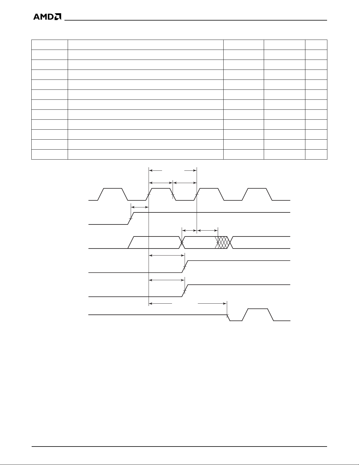
DATA SHEET
Table 36. 10 Mbps MII Transmit Timing
Symbol Parameter Description Min. Max. Unit
t
MTS10
t
MTH10
t
MTEP10
t
MTECRH10
t
MTECOH10
t
MTDCRL10
t
MTDCOL10
t
MTIDLE10
t
MTP10
t
MTWH10
t
MTWL10
TX_EN, TXD10[3:0] Setup Time to TX_CLK Rising Edge 12 - ns
TX_EN, TXD10[3:0] Hold time From TX_CLK Rising Edge 0 - ns
Transmit Latency TX_EN Sampled by TX_CLK to Start of Packet 240 360 ns
CRS Assert from TX_EN Sampled HIGH - 130 ns
COL Assert from TX_EN Sampled HIGH - 300 ns
CRS De-assert From TX_EN Sampled LOW - 130 ns
COL De-assert From TX_EN Sampled LOW - 130 ns
Required De-assertion Time Between Packets 300 - ns
TX_CLK Period 399.98 400.02 ns
TX_CLK HIGH 180 220 ns
TX_CLK LOW 180 220 ns
t
MTP10
TX_CLK
TX_EN
TXD[3:0]
CRS
COL
TX±
t
t
MTS10
t
MTECRH10
t
MTECLH10
MTWH10
t
MTS10
t
MTEP10
t
MTWL10
t
MTH100
Figure 22. 10 Mbps MII Transmit Start of Packet Timing
22236G-24
52 Am79C874 22235K
Page 53

TX_CLK
TX_EN
CRS
COL
DATA SHEET
t
MTIDLE10
t
MTDCRL10
t
MTDCOL10
TX±
22236G-25
Figure 23. 10 Mbps MII Transmit End of Packet Timing
22235K Am79C874 53
Page 54

DATA SHEET
Table 37. 10 Mbps MII Receive Timing
Symbol Parameter Description Min. Max. Unit
t
MRPCRH10
t
MRPCOH10
tMRCHR10
t
MRRC10
t
MRCRD10
t
MRECRL10
t
MRECOL10
t
MRERL10
CRS HIGH After Start of Packet 80 150 ns
COL HIGH After Start of Packet 80 150 ns
RXD[3:0], RX_DV, RX_ER Valid after CRS HIGH 100 100 ns
RXD[3:0], RX_DV, RX_ER Valid Prior to the Rising of RX_CLK10 16 - ns
RXD[3:0], RX_DV, RX_ER Valid After the Rising Edge of RX_CLK 12 - ns
End of Packet to CRS LOW 130 190 ns
End of Packet to COL LOW 125 185 ns
End of Packet to RXD[3:0], RX_DV, RX_ER De-Asserting (Going
LOW)
RX±
t
MRPCRH10
CRS
120 140 ns
COL
RX_CLK
RXD[3:0]
RX_DV
RX_ER
RX±
CRS
COL
t
MRPCOH10
t
t
MRCHR10
MRRC10
t
MRCR10
Figure 24. 10 Mbps MII Receive Start of Packet Timing
t
MRECRL10
t
MRECOL10
22236G-26
RX_CLK
t
MRERL10
RXD[3:0]
RX_DV
RX_ER
22236G-27
Figure 25. 10 Mbps MII Receive End of Packet Timing
54 Am79C874 22235K
Page 55

DATA SHEET
GPSI Signals
Table 38. 10 Mbps GPSI Receive Timing
Symbol Parameter Description Min. Max. Unit
t
GCD
t
GRCD
10CRS HIGH To First Bit Of Data 750 850 ns
Rising Edge of 10RXCLK to 10RXD or 10CRS 45 55 ns
RX ±
10CRS
10RXCLK
10RXD
Bit Cell 1
1
10 1 0 1
t
GRCD
Bit Cell 20Bit Cell 31Bit Cell 40Bit Cell 5
1
t
GCD
t
GRCD
22236G-28
Figure 26. GPSI Receive Timing - Start of Reception
Table 39. 10 Mbps GPSI Receive Timing
Symbol Parameter Description Min. Max. Unit
t
GRCD
Rising Edge of 10RXCLK to 10RXD or 10CRS 45 55 ns
RX±
10CRS
10RXCLK
10RXD
1
Bit (N _ 1)
t
GRCD
Bit (N _ 1)
0
Bit N
Bit N
t
GRCD
Figure 27. GPSI Receive Timing - End of Reception (Last Bit = 0)
22236G-29
22235K Am79C874 55
Page 56
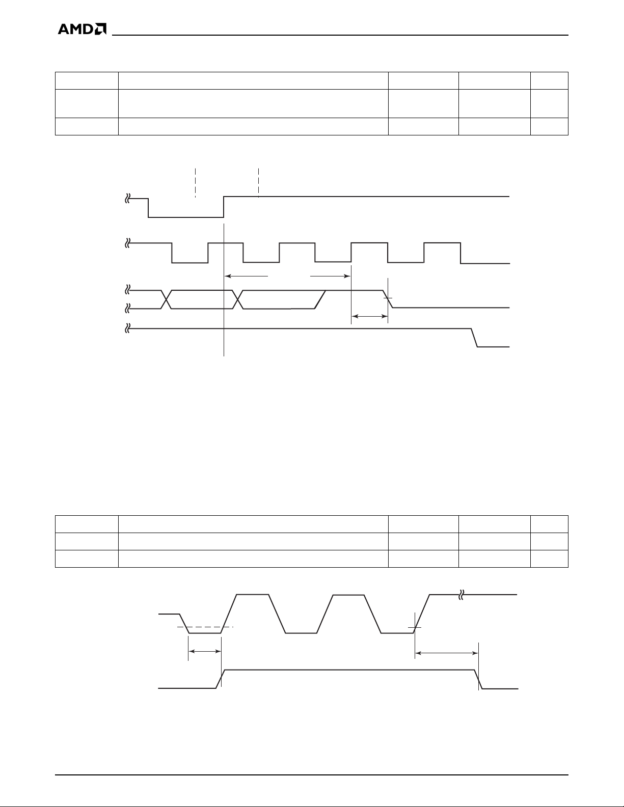
DATA SHEET
Table 40. 10 Mbps GPSI Receive Timing
Symbol Parameter Description Min. Max. Unit
t
GDOFF
t
GRCD
Delay from RX± going to 1 to the Rising Edge of 10RXCLK, which
clocks out the last bit of data on 10RXD
190 ns
Rising Edge of 10RXCLK to 10RXD or 10CRS 45 55 ns
RX ±
10RXCLK
10RXD
10CRS
0
Bit (N _ 1)
1
Bit N
t
GDOFF
Bit (N _ 1)
Bit N
t
GRCD
Figure 28. GPSI Receive Timing - End of Reception (Last Bit = 1)
22236G-30
Table 41. 10 Mbps GPSI Collision Timing
Symbol Parameter Description Min. Max. Unit
t
GCSCLH
t
GCECLL
Collision Start to 10COL HIGH 80 150 ns
Collision End to 10COL LOW 125 185 ns
Collision
0 V
+
Presence±
t
GCSCLH
t
GCECLL
10COL
22236G-31
Figure 29. GPSI Collision Timing
56 Am79C874 22235K
Page 57

DATA SHEET
Table 42. 10 Mbps GPSI Transmit Timing
Symbol Parameter Description Min. Max. Unit
t
GTTX
Delay from the rising edge of the 10TXCLK which first clocks
10TXEN HIGH to TX± toggling LOW
10TXCLK
240 360 ns
10TXEN
t
GTTX
TX±
22236G-32
Figure 30. GPSI Transmit Timing - Start of Transmission
Table 43. GPSI Transmit 10TXCLK and 10TXD Timing
Symbol Parameter Description Min. Max. Unit
t
GTC DH
t
GDTCS
t
GTC H
t
GTC L
t
GTC P
10TXCLK to 10TXD or 10TXEN Hold Time 20 ns
10TXD or 10TXEN to 10TXCLK Setup Time 20 ns
10TXCLK Width HIGH 45 55 ns
10TXCLK Width LOW 45 55 ns
10TXCLK Period 99,995 100,005 ns
t
GTCP
t
GTCH
t
GTCL
10TXCLK
t
GTCDH
10TXD
t
t
GDTCS
GTCDH
10TXEN
22235E-36
Figure 31. GPSI Transmit 10TXCLK and 10TXD Timing
DUT
50 pF
22235E-37
Figure 32. Test Load for 10RXD, 10CRS, 10RXCLK, 10TXCLK and 10COL
22235K Am79C874 57
Page 58

PHYSICAL DIMENSIONS
PQT80 (measured in millimeters)
80-Lead Thin Plastic Quad Flat Pack (PQT)
DATA SHEET
Dwg rev. AE; 8/99
PQT80
58 Am79C874 22235K
Page 59

DATA SHEET
ERRATA FOR REVISION [B.7] SILICON
NetPHY-1LP Revision B.7 is the current production revision silicon with errata– please refer to the descriptions below.
Revision [B.7] Errata Summary
The NetPHY-1LP device has a total of 3 errata, all of
which are minor and should not cause concern.
All information below should be used in conjunction
with the latest NetPHY-1LP Datasheet PID 22235,
available on the AMD website (www.amd.com).
Errata for NetPHY-1LP [B.7]
The SYMPTOM section gives an external description
of the problem. The IMPLICATION section explains
how the device behaves and its impact on the system.
The WORKAROUND section describes a workaround
for the problem. The STATUS section indicates when
and how the problem will be fixed.
B7 Errata 1- Advanced LED Mode Activity
SYMPTOM:
In Advanced LED mode, the two bi-color LEDs show
Link status by turning on, Speed status by which bicolor LED turns on, and Duplex status by their color.
Activity is shown by blinking the bi-color LED off for
one-fourth of a second. If set to show TX and RX activity in Half Duplex, the bi-color LED will remain turned
off for the duration of the packet burst if TX and RX are
in opposite phase.
WORKAROUND:
1. Set Register 21, Bit 10 to 1. This will cause the Activity blink to occur only for RX in Half Duplex (just
like Full Duplex).
2. Use Normal LED mode to ensure accurate Link and
Activity LED status in Half Duplex mode.
STATUS:
This errata will not be fixed.
B7 Errata 2 - Auto-Negotiation ACK Bit
SYMPTOM:
During Auto-Negotiation, the ACK bit is set regardless
of the time interval between the FLP burst received.
WORKAROUND:
None. It is unlikely that the other device will incorrectly
generate FLPs.
STATUS:
This errata will not be fixed.
B7 Errata 3 - Missing or Distorted /T/R/
SYMPTOM:
The device accepts frames without the proper End Of
Stream delimiter /T/R/.
WORKAROUND:
None. It is unlikely that the other device will generate
this error. It could be generated by a noise event in the
cable occurring in this specific location of a packet.
The effect would be to add 8 dribbling bits to the end of
the packet. The MAC will catch this as an alignment
error or a CRC error.
STATUS:
This errata will not be fixed.
22235K Am79C874 59
Page 60

DATA SHEET
REVISION SUMMARY
Revisions to other versions this document are presented in the following table.
Table 44. Revision Summary
Revision Summary of Changes
D • Corrected reversal of Figure 4 and Figure 5 in LED section.
• Changed ECL to PECL.
E • Added GPSI timing and diagrams
• Added Industrial Temperature support
F • Minor edits
G • Minor edits
H • PHYAD pins: Specified using resistors in the range of 1 kΩ to 4.7 kΩ for setting PHYAD pins. In GPSI mode,
PHYAD pins must be set to addresses other than 00h.
• DC Characteristics added: V
• DC Characteristics, added new values for: IIL, IIH, I
LED component changes.
I • Added clarification to RX_CLK throughout document, which is active only while LINK is established. See pin
description for more information.
• Added Flow Control descriptions to registers 4 and 5
• Register 21, bit 9 was reversed: 1 selects the standard LED configuration, while 0 selects the advanced LED
configuration
• Register 21, bit 2 was changed to indicate EN_SCRM, Scrambler Enable; a 1 enables the scrambler. This register
is set by the SCRAM_EN pin
• Maximum input voltage is 5.5 V; operating voltage for 5-V tolerant pins is 5.0 V
• Minor edits
J • Changed resistor requirements to 1K to 4.7
• Minor clarifications to pin descriptions.
• Clarified GPSI/7-Wire mode operation.
• Changed Figure 1, 100BASE-FX termination.
• Clarified loopback section.
• Changes RESET minimum time to 155 µs from 10 ms.
• LEDs - replaced Tables 7, 8, and 9, added to clarify Advanced LED Mode Operation. Modfied Figure 5 and added
note #3.
• Clarified Register 0, bit 15 RESET
• Default for Register 16, bit 10 is 0 (Loopback)
• Clarified Register 21, bit 10, Advanced LED Mode Configuration.
• Register 23 (Disconnect Counter) only applicable to 100 Mbps operation.
K • Updated “Ordering Information” on page 4.
OLL
and V
OHL
Figure 6, Advanced LED Configuration, changes to Receive
OZ.
kΩ instead of 10 kΩ in most cases.
The contents of this document are provided in connection with Advanced Micro Devices, Inc. (“AMD”) products. AMD makes no representations or warranties with respect to the accuracy or
completeness of the contents of this publication and reserves the right to make changes to specifications and product descriptions at any time without notice. No license, whether express,
implied, arising by estoppel or otherwise, to any intellectual property rights is granted by this publication. Except as set forth in AMD's Standard Terms and Conditions of Sale, AMD assumes
no liability whatsoever, and disclaims any express or implied warranty, relating to its products including, but not limited to, the implied warranty of merchantability, fitness for a particular purpose,
or infringement of any intellectual property right.
AMD's products are not designed, intended, authorized or warranted for use as components in systems intended for surgical implant into the body, or in other applications intended to support
or sustain life, or in any other application in which the failure of AMD's product could create a situation where personal injury, death, or severe property or environmental damage may occur.
AMD reserves the right to discontinue or make changes to its products at any time without notice.
Trademarks
Copyright © 1999, 2000, 2001, 2004, 2005 Advanced Micro Devices, Inc. All rights reserved.
AMD, the AMD logo and combinations thereof, PCnet-PRO, PCnet-FAST, PCnet-Home, PowerWise and NetPHY are trademarks of Advanced Micro Devices, Inc.
Other product names used in this publication are for identification purposes only and may be trademarks of their respective companies.
60 Am79C874 22235K
 Loading...