


■
■
■
■
■
■
■
■
■
■
■
■
FINAL
Am79C100
Twisted-Pair Ethernet Transceiver Plus (TPEX Plus)
DISTINCTIVE CHARACTERISTICS
CMOS device provides IEEE 802.3-compliant
operation and low operating current from a
single +5 V supply
Power Down mode for reduced power
consumption in battery-powered applications
Automatic twisted-pair link integrity
Pin-selectable twisted-pair receive polarity
detection and automatic inversion of the receive
signal. Polarity indication output pin can
directly drive an LED.
Pin-selectable twisted-pair link integrity test
capability conforming to the IEEE 802.3
standard. Link status pin can directly drive
an LED.
Transmit, receive, and collision status
indications available on separate, dedicated
pins
Outputs can directly drive LEDs with pulses
stretched to ensure LED visibility
Internal twisted-pair transmitter digital
predistortion circuit to reduce medium-induced
jitter
Pin-selectable SQE Test (heartbeat) enable
AUI loopback, Jabber Control, and SQE Test
functions comply with the 10BASE-T standard
User-selectable loopback operations
Pin-selectable twisted-pair receive threshold
programming for extended distance line lengths
GENERAL DESCRIPTION
The Am79C100 Twisted-Pair Ethernet Transceiver Plus
(TPEX Plus) is an integrated circuit that implements the
medium attachment unit (MAU) functions for the
twisted-pair medium, as specified by the supplement to
the IEEE 802.3 standard (Type 10BASE-T). This device provides the necessary electrical and functional
interface between the IEEE 802.3 standard attachment
unit interface (AUI) and the twisted-pair cable.
A network based on the 10BASE-T standard can use
unshielded twisted-pair cables, providing an economical solution to networking by allowing the use of existing
telephone wiring. The Am79C100 provides a minimal
component count and a cost-effective solution to the
design and implementation of 10BASE-T standard
networks.
TPEX Plus provides twisted-pair driver and receiver circuits, including on-board transmit digital predistortion,
receiver squelch, and an AUI port with pin-selectable
SQE Test enable. The device provides a number of additional features, including Link Status indication with
automatic twisted-pair receive polarity detection/
correction and indication; pin-selectable receive
threshold programming for extended distance line
lengths; and Receive Carrier Sense, Transmit Active
and Collision Present indications. The device provides
separate twisted-pair Link Status, Polarity Status,
Receive, Transmit, and Collision outputs to drive LEDs
directly.
Publication# 16511 Rev: BAmendment/0
Issue Date: May 1994
1
AMD
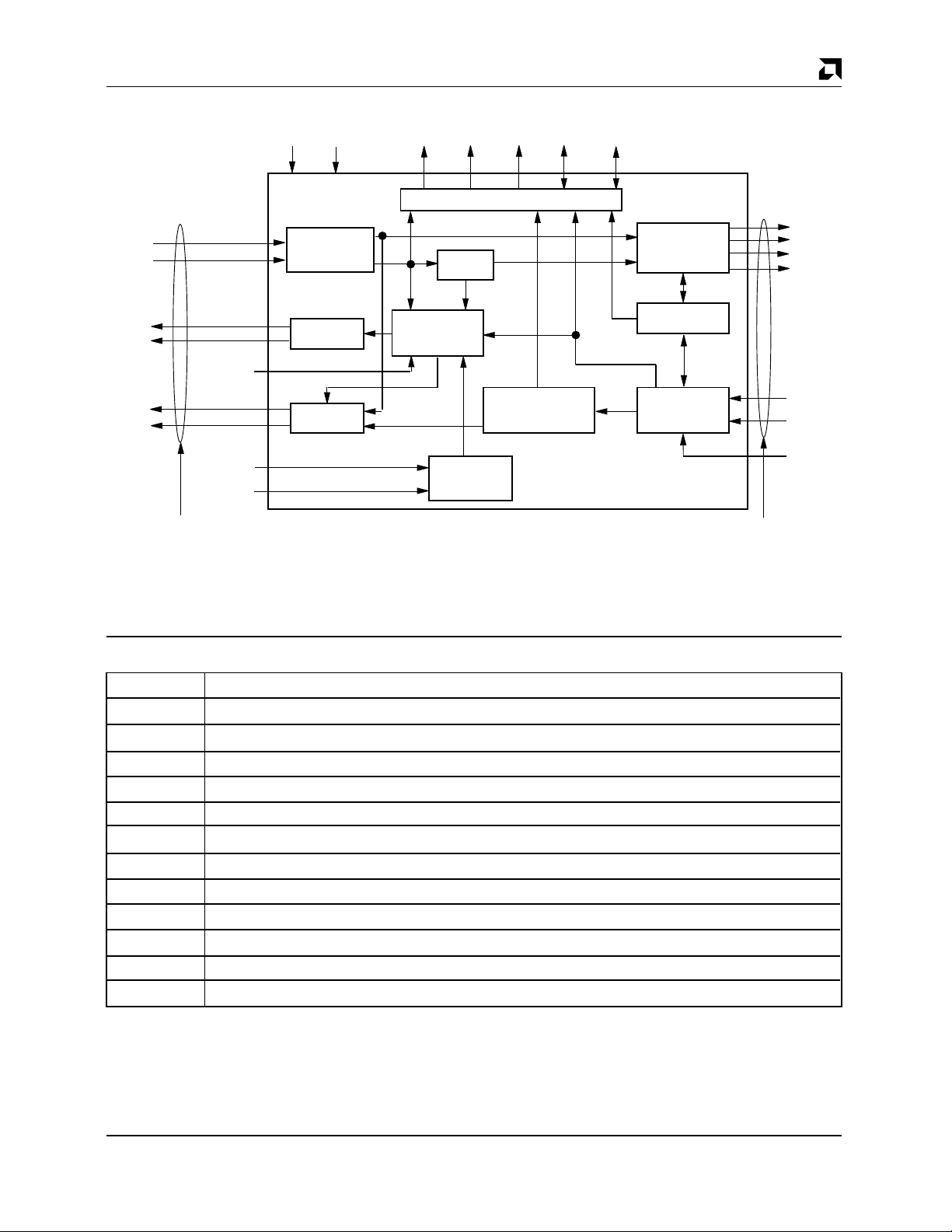
BLOCK DIAGRAM
DO+
DO–
CI+
CI–
DI+
DI–
Attachment
Unit Interface
SQE TEST
PRDN/RST
(AUI)
REXT
TEST1TEST2
Line Receiver
and Squelch
Circuit
Line Driver
Line Driver
XMT COL RCV LNKST
RXPOL
LED Driver Logic
Jabber
Control
Collision and
Loopback
Control
Polarity
Detection and
Auto Correction
Voltage
Controlled
Oscillator
Line Driver
and
Predistortion
Link Test
State Machine
Line Receiver
and
Smart Squelch
TXD+
TXD–
TXP+
TXP–
RXD+
RXD–
LRT
Twisted-Pair
Interface
RELATED AMD PRODUCTS
Part No. Description
Am7996 IEEE-802.3/Ethernet/Cheapernet Tap Transceiver
TM
)
TM
(C-LANCE)
TM
(ILACCTM)
TM
(HIMIBTM)
Plug n’ Play support)
Am79C90 CMOS Local Area Network Controller for Ethernet
Am79C900 Integrated Local Area Communications Controller
Am79C940 Media Access Controller for Ethernet (MACE
Am79C960 PCnet-ISA Single-Chip Ethernet Controller (for ISA bus)
Am79C961 PCnet-ISA Single-Chip Ethernet Controller (with Microsoft
Am79C965 PCnet-32 Single-Chip Ethernet Controller (for 386DX, 486 and VL buses)
Am79C970 PCnet-PCI Single-Chip Ethernet Controller (for PCI bus)
Am79C974 PCnet-SCSI Combination Ethernet and SCSI Controller for PCI Systems
Am79C98 Twisted-Pair Ethernet Transceiver (TPEX)
Am79C981 Integrated Multiport Repeater Plus
TM
(IMR+TM)
Am79C987 Hardware Implemented Management Information Base
16511B-1
2 Am79C100
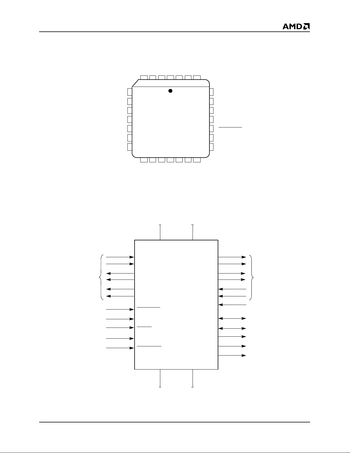
CONNECTION DIAGRAM
DI–
DI+
PLCC
CI–
CI+
TXD+
TXD–
TXP+
LOGIC SYMBOL
DV
DV
XMT
LNKST
COL
AV
DO+
SS
SS
SS
6
7
8
9
10
11
121314
DO–
234
1
RCV
REXT
PRDN/RST
DV
DD
2827
1615
RXPOL
AV
26
1817
RXD–
DD
255
24
23
22
21
20
19
RXD+
TXP–
DV
DD
TEST2
TEST1
SQE TEST
LRT
AV
DD
16511B-2
Attachment
Unit Interface
(AUI)
DO+
DO–
DI+
DI–
CI+
CI–
SQE
TEST
TEST1
TEST2
REXT
PRDN/RST
DV
Am79C100
SS
AV
SS
TXD+
TXP+
TXD–
TXP–
RXD+
RXD–
LRT
RXPOL
LNKST
XMT
RCV
COL
Twisted-Pair
Interface
16511B-3
Am79C100 3
ORDERING INFORMATION
Standard Products
AMD standard products are available in several packages and operating ranges. The order number (valid combination) is formed
by a combination of the elements below.
AM79C100 J C
DEVICE NUMBER/DESCRIPTION
Am79C100
Twisted-Pair Ethernet Transceiver Plus (TPEX Plus)
Valid Combinations
AM79C100 JC
OPTIONAL PROCESSING
Blank = Standard Processing
OPERATING CONDITIONS
C = Commercial (0°C to +70°C)
PACKAGE TYPE
J = 28-Pin Plastic Leaded Chip Carrier (PL 028)
SPEED
Not Applicable
Valid Combinations
Valid combinations list configurations planned to be supported in volume for this device. Consult the local AMD sales
office to confirm availability of specific valid combinations and
to check on newly released combinations.
4 Am79C100
PIN DESCRIPTION
AV
DD
Analog Power
This pin supplies +5 V to analog portions of the TPEX
Plus circuitry.
AV
SS
Analog Ground
This pin is the ground reference for analog portions of
TPEX Plus circuitry.
CI+, CI–
Control In
Output
AUI port differential driver.
COL
Collision
Output, Open Drain
This pin is driven LOW while the TPEX Plus is simultaneously receiving data on the AUI DO pins and the
twisted-pair RXD pins, indicating that a collision condition exists. It is also driven if TPEX Plus enters the jabber condition due to excessive length of activity on the
DO pair. In this case TPEX Plus will wait for a period of
inactivity on DO for the “unjab” time of 250 to 750 ms,
before the 10 MHz pattern on the CI pair is removed
and COL
SQE Test activity on the AUI CI pair. In the LOW output
state, the pin is capable of sinking a maximum of 12 mA
and can be used to drive an LED. The COL output is
pulse stretched for 20 to 62 ms after the end of collision, to ensure LED visibility.
returns inactive. COL will not be driven during
DI+, DI–
Data In
Output
AUI port differential driver.
DO+, DO–
Data Out
Input
AUI port differential receiver.
DV
DD
Digital Power
This pin supplies +5 V to digital portions of the TPEX
Plus circuitry, including all transmit drivers.
DV
SS
Digital Ground
Two pins provide the ground reference for digital portions of TPEX Plus circuitry, including all transmit
drivers and the status indication LED drivers.
LNKST
Link Status
Input/Output, Open Drain
When this pin is tied LOW, the internal Link Test Receive function is disabled, and the Transmit and
Receive functions will remain active regardless of arriving idle link pulses and data. TPEX Plus continues to
generate idle link pulses irrespective of the status of
this pin.
As an output, this pin is driven LOW if the link is identified as functional. However, if the link is determined to
be nonfunctional due to missing idle link pulses or data
packets, then this pin is not driven (internally pulled
HIGH). In the LOW output state, the pin is capable of
sinking a maximum of 12 mA and can be used to drive
an LED.
In the absence of an external drive, the pin is internally
pulled HIGH when inactive.
LR
T
Low Receive Threshold
Input, Active LOW
When this pin is tied LOW, the internal twisted-pair receive thresholds are reduced by 4.5 dB from their original values (approximately 3/5 of the normal 10BASE-T
value). With LR
threshold for the RXD ± circuit will be 300 mV to 520 mV
peak. With LRT in the LOW state, the unsquelch
threshold for the RXD ± circuit will be 180 mV to 312 mV
peak. In either case, the RXD ± circuit post unsquelch
threshold will be approximately one-half of the initial
unsquelch threshold.
T in the HIGH state, the unsquelch
PRDN/RST
Power Down/Reset
Input, Active LOW
Driving this input LOW resets the internal logic of TPEX
Plus and places the device in a special Power Down
mode. In the Power Down/Reset mode, all output drivers are placed in their inactive state.
REXT
External Resistor
Input
An external precision resistor is connected between
this pin and AV
ence for the internal voltage-controlled oscillator
(VCO).
in order to provide a current refer-
DD
RCV
Receive
Output, Open Drain
This pin is driven LOW while TPEX Plus is receiving
data on the twisted-pair RXD pins and is transferring
the received signal onto the AUI DI pair. The output is
LOW during collision simultaneously with the COL
pin.
Am79C100 5
In the LOW output state, the pin is capable of sinking a
maximum of 12 mA and can be used to drive an LED.
The RCV
after the end of reception, to ensure LED visibility.
output is pulse stretched for 20 ms to 62 ms
RXD+, RXD–
Receive Data
Input
10BASE-T port differential receiver.
RXPOL
Receive Polarity
Input/Output, Open Drain
The twisted-pair receiver is capable of detecting a receive signal with reversed polarity (wiring error). The
RXPOL pin is normally in the LOW state, indicating correct polarity of the received signal. If the receiver detects a received packet with reversed polarity, then this
pin is not driven (goes HIGH) and the polarity of subsequent packets is inverted. In the LOW output state, this
pin can sink up to a maximum of 12 mA and is therefore
capable of driving an LED.
This feature can be disabled by strapping this pin LOW.
In this case, the Receive Polarity correction circuit is
disabled and the internal Receive Signal remains noninverted, irrespective of the received signal.
In the absence of an external drive, the pin is internally
pulled HIGH when inactive.
SQE
TEST
Signal Quality Test (Heartbeat) Enable
Input, Active LOW
The SQE Test function is enabled by tying this input
LOW. When enabled, TPEX Plus will send a 10 MHz
burst (heartbeat) on the CI ± lines after DO ± has become inactive, indicating integrity of the collision detection and AUI circuitry. SQE
repeater applications.
In the absence of an external drive, the pin is internally
pulled HIGH when inactive.
TEST should be disabled for
TEST1
Test
Input, Active HIGH
This pin should be tied LOW for normal operation.
TEST1 permits system-level diagnostics to be performed. If TEST1 is driven HIGH (while TEST2
tained HIGH), TPEX Plus will enter the Loopback Test
mode. The type of loopback is determined by the state
of the SQE TEST pin. If SQE TEST is in the LOW state
is main-
(Station MAU), TPEX Plus transfers data independently from DO to the TXD/TXP circuits and from RXD
to the DI circuit. If the SQE
(Repeater MAU), then data on the RXD circuit is transmitted back onto the TXD/TXP circuits and data on the
DO circuit is transmitted onto the DI pair.
During either test mode, the Collision Detection and
SQE Test functions are disabled, and CI ± will remain
idle. Link beat pulses will continue to be generated normally in the absence of TXD/TXP output activity, and
the Link Test Receive State Machine will be forced into
the Link Pass state. The COL
whenever a link beat pulse or transmit data activity
commences, and remain low during the output activity.
The receive squelch will continue to operate on both
the RXD ± and DO ± input circuits.
In the absence of an external drive, the pin is internally
pulled LOW.
TEST is in the HIGH state
pin will be driven LOW
TEST2
Test
Input, Active LOW
This pin should be tied HIGH for normal operation.
is reserved for factory testing, and should be
TEST2
permanently tied HIGH.
In the absence of an external drive, the pin is internally
pulled HIGH.
TXD+, TXD–
Transmit Data
Output
10BASE-T port differential drivers.
TXP+, TXP–
Transmit Predistortion
Output
Transmit waveform differential driver for predistortion.
XMT
Transmit
Output, Open Drain
This pin is driven LOW while TPEX Plus is receiving
data on the AUI DO pair and is transmitting data on the
TXD/TXP pins. The output is LOW during collision simultaneously with the COL
state, the pin is capable of sinking a maximum of 12 mA
and can be used to drive an LED. The XMT output is
pulse stretched for 20 to 62 ms after the end of transmission, to ensure LED visibility.
pin. In the LOW output
6 Am79C100

FUNCTIONAL DESCRIPTION
The Twisted-Pair Ethernet Transceiver Plus (TPEX
Plus) complies with the requirements specified by the
IEEE 802.3 standard for the attachment unit interface
(AUI) and the 10BASE-T standard for a twisted-pair
medium attachment unit (MAU). TPEX Plus also implements a number of features in addition to the IEEE
802.3 standard. An outline of the functions of the
Am79C100 is given below.
Attachment Unit Interface (DO ± , DI ± , CI ± )
The AUI electrical and functional characteristics comply with those specified within the IEEE 802.3 documents, Sections 7 and 14. The AUI pins can be wired
to an isolation transformer, for a remote MAU application, or directly to another device (e.g., Am7992B serial
interface adapter), in the case of a local DTE application. The end-of-packet SQE Test function (heartbeat)
can be disabled to allow the device to be employed in a
repeater application.
Twisted-Pair Transmit Function
Data transmission to the 10BASE-T medium occurs
when valid AUI signals appear on the DO ± differential
pair. This data stream is routed to the differential driver
circuitry in the TXD ± and TXP ± pins. The driver circuitry
provides the necessary electrical driving capability and
the predistortion control for transmitting signals over
maximum length twisted-pair cable, as specified by the
IEEE 802.3 10BASE-T standard. During transmission,
data is looped back to the DI ± differential circuit, indicating normal operation. The transmit function for data
output and loopback operations meets the propagation
delays and jitter specified by the standard. During normal transmission, and providing that TPEX Plus is not
in a Link Fail or Jabber state, the XMT pin will be driven
LOW, and can be used to drive a status LED directly.
Twisted-Pair Receive Function
The receiver complies with the receiver specifications
of the IEEE 802.3 10BASE-T standard, including noise
immunity and received signal rejection criteria (“Smart
Squelch”). Signals meeting these criteria appearing at
the RXD ± differential input pair are routed to the DI ±
outputs. The receiver function meets the propagation
delays and jitter requirements specified by the standard. The receiver squelch level drops to approximately
half its threshold value after unsquelch to allow reception of minimum amplitude signals and to mitigate carrier fade in the event of worst-case signal attenuation
and crosstalk noise conditions. During receive, the
RCV pin is driven LOW and can be used to drive a status LED directly.
Note that the 10BASE-T standard defines the receive
input amplitude at the external media-dependent interface (MDI). Filter and transformer loss are not specified. The TPEX Plus receiver squelch levels are defined
to account for a 1 dB insertion loss at 10 MHz, which is
typical for the type of receive filters/transformers recommended (see also Table 1).
Normal 10BASE-T-compatible receive thresholds are
employed when the LR
the LRT pin is externally pulled LOW, the Low Receive
Threshold option is invoked, and the sensitivity of the
TPEX Plus receiver is increased. This allows longer
line lengths to be employed, exceeding the 100 m target distance of normal 10BASE-T (assuming typical 24
AWG cable). The additional cable distance contributes
directly to increased signal attenuation and reduced
signal amplitude at the TPEX Plus receiver. However,
from a system perspective, making the receiver more
sensitive means that it is also more susceptible to
extraneous noise, primarily caused by coupling from
co-resident services (crosstalk). For this reason, it is
recommended that when using the Low Receive
Threshold option, the service should be installed on
4-pair cable only. Multipair cables within the same outer
sheath have lower crosstalk attenuation, may allow
noise emitted from adjacent pairs to couple into the receive pair, and be of sufficient amplitude to falsely unsquelch the TPEX Plus.
T pin is inactive (HIGH). When
Link Test Function
The Link Test function is implemented as specified by
the 10BASE-T standard. During periods of transmit
pair inactivity, “link beat” pulses will be sent periodically
over the twisted-pair medium to allow constant monitoring of medium integrity.
When the Link Test function is enabled, the absence of
link beat pulses and receive data on the RXD ± pair will
cause the TPEX Plus to go into a Link Fail state. In the
Link Fail state, data transmission, data reception, data
loopback, and collision detection functions are disabled
and remain disabled until valid data or >5 consecutive
link pulses appear on the RXD ± pair. During Link Fail,
the LNKST pin is internally pulled HIGH. When the link
is identified as functional, the LNKST pin is driven
LOW, and is capable of directly driving a “Link OK”
LED. In order to interoperate with systems that do not
implement Link Test, this function can be disabled by
grounding the LNKST pin. With Link Test disabled, the
data driver, receiver, and loopback functions, as well as
collision detection, remain enabled irrespective of the
presence or absence of data or link pulses on the
RXD ± pair.
Polarity Detection and Reversal
The TPEX Plus receive function includes the ability to
invert the polarity of the signals appearing at the RXD ±
pair if the polarity of the received signal is reversed
(such as in the case of a wiring error). This feature allows data packets received from a reverse-wired RXD ±
input pair to be corrected in the TPEX Plus prior to
transfer to the DTE via the AUI interface (DI ± ). The
Am79C100 7
polarity detection function is activated following reset or
Link Fail, and will reverse the receive polarity based on
both the polarity of any previous link beat pulses and
the polarity of subsequent packets with a valid end
transmit delimiter (ETD).
When in the Link Fail state, TPEX Plus will recognize
link beat pulses of either positive or negative polarity.
Exit from the Link Fail state is caused by the reception
of 5 to 6 consecutive link beat pulses of identical polarity. On entry to the Link Pass state, the polarity of the
last 5 link beat pulses is used to determine the initial receive polarity configuration and the receiver is reconfigured to subsequently recognize only link beat pulses of
the previously recognized polarity. This link pulse algorithm is employed only until SFD polarity determination
is made, as described later in this section.
Positive link beat pulses are defined as received signal
with a positive amplitude greater than 520 mV (LR
HIGH) with a pulse width of 60 ns to 200 ns. This positive excursion may be followed by a negative excursion.
This definition is consistent with the expected received
signal at a correctly wired receiver, when a link beat
pulse that fits the template of Figure 14-12 in the
10BASE-T standard is generated at a transmitter and
passed through 100 m of twisted-pair cable.
Negative link beat pulses are defined as received signals with a negative amplitude greater than 520 mV
(LRT = HIGH) with a pulse width of 60 ns to 200 ns.
This negative excursion may be followed by a positive
excursion. This definition is consistent with the expected received signal at a reverse-wired receiver,
when a link beat pulse that fits the template of Figure
14-12 in the 10BASE-T standard is generated at a
transmitter and passed through 100 m of twisted-pair
cable.
The polarity detection/correction algorithm will remain
“armed” until two consecutive packets with valid ETD of
identical polarity are detected. When “armed,” the receiver is capable of changing the initial or previous polarity configuration based on the most recent ETD
polarity.
On receipt of the first packet with valid ETD following
reset or Link Fail, TPEX Plus will utilize the inferred polarity information to configure its RXD ± input, regardless of its previous state. On receipt of a second packet
with a valid ETD with correct polarity, the detection/correction algorithm will “lock in” the received polarity. If
the second (or subsequent) packet is not detected as
confirming the previous polarity decision, the most recently detected ETD polarity will be used as the default.
Note that packets with invalid ETD have no effect on
updating the previous polarity decision. Once two consecutive packets with valid ETD have been received,
TPEX Plus will disable the detection/correction
T =
algorithm until either a Link Fail condition occurs or
PRDN/RST
During polarity reversal, the RXPOL pin is internally
pulled HIGH. During normal polarity conditions, the
RXPOL pin is driven LOW, and is capable of directly
driving a “Polarity OK” LED using an integrated 12 mA
driver. If desired, the Polarity Reversal function can be
disabled by grounding the RXPOL pin.
is asserted.
Twisted-Pair Interface Status
Three outputs (XMT
the TPEX Plus is transmitting (AUI to twisted-pair), receiving (twisted-pair to AUI), or in a collision state with
both functions active simultaneously.
The TPEX Plus will power up in the Link Fail state. The
normal algorithm will apply to allow it to enter the Link
Pass state. On power up, the XMT
drivers activate for 20 ms to 62 ms as a lamp test feature, and will then go to their inactive state until TPEX
Plus enters the Link Pass state.
In the Link Pass state, transmit or receive activity that
passes the pulse-width/amplitude requirements of the
DO± or RXD± inputs will be indicated by the XMT or
RCV pin, respectively, going active. XMT, RCV, and
COL are all asserted during a collision.
In the Link Fail state, XMT , RCV, and COL are disabled.
In Jabber Detect mode, TPEX Plus will activate the
COL driver, disable the XMT driver (regardless of DO±
activity), and allow the RCV driver to indicate the current state of the RXD± pair. If there is no receive activity
on RXD±, only COL will be active during Jabber Detect.
If there is RXD± activity, both COL and RCV will be
active.
All three outputs are active LOW and incorporate 12
mA drive capability with 20 ms to 62 ms pulse stretch
circuitry, to extend the event to ensure LED visibility.
, RCV, and COL) indicate whether
, RCV, and COL LED
Collision Detect Function
Simultaneous Carrier Sense (presence of valid data
signals) by both the AUI DO± pins and the twisted-pair
RXD± pins constitutes a collision, thereby causing a
10 MHz signal to be asserted on the CI± output pair,
and the COL output to be activated. The CI± output
meets the drive requirements for the AUI interface. This
10 MHz signal will remain on the CI± pair until one of
the two colliding states changes from active to idle.
During the collision condition, data presented on the
DI± pair will be sourced from the RXD± input. At the
end of collision, the data presented on the DI± pair will
be sourced from the last remaining active input, either
RXD± or DO±. The CI± output pair stays HIGH for 2 bit
times at the end of a collision, decreasing to the idle
level within 80 bit times after the last transition. The
XMT, RCV, and COL pins are driven LOW during
collision.
8 Am79C100

Signal Quality Error (SQE) Test (Heartbeat)
Function
When the SQE TEST pin is driven LOW, TPEX Plus will
routinely exercise the collision detection circuitry by
generating an SQE Test message at the end of every
transmission. This signal is a self-test indication to the
DTE that the MAU collision circuitry is functional and
the AUI cable/connection is intact. An SQE Test message consists of a 10 MHz signal on the CI± pair with a
duration of 5 to 15 bit times (500 ns to 1500 ns). When
enabled, an SQE Test will occur at the end of every
transmission, starting 6 to 16 bit times (600 ns to
1600 ns) after the last transition of the transmitted signal. For repeater applications, the SQE Test function
can be disabled by tying the SQE
leaving it disconnected. The COL output will remain inactive during the SQE Test message on CI±.
TEST pin HIGH or by
Jabber Function
The Jabber function inhibits the twisted-pair transmit
function of TPEX Plus if the DO± circuit is active for an
excessive period (20 ms to 150 ms). This prevents any
one node from disrupting the network due to a
“stuck on” or faulty transmitter. If this maximum transmit time is exceeded, the TPEX Plus transmitter circuitry is disabled and a 10 MHz signal is driven onto the
CI± pair. Once the transmit data stream is removed
from the DO± input pair, an “unjab” time of 250 ms to
750 ms will elapse before the TPEX Plus removes the
10 MHz signal from the CI± pair and re-enables the
transmit circuitry.
When jabber is detected, TPEX Plus will activate the
COL driver, disable the XMT driver (regardless of DO±
activity), and allow the RCV driver to indicate the
current state of the RXD± pair. If there is no receive activity on RXD±, only COL will be active during Jabber
Detect. If there is RXD± activity, both COL and RCV will
be active.
Power Down
In addition to on-board power-on-reset circuitry, the
PRDN/RST pin is used as the master reset for TPEX
Plus. PRDN/RST must be driven LOW for a minimum
of 2 µs for reset to occur. The PRDN/RST pin can also
be used to put the TPEX Plus into an inactive or “sleep”
state, causing the device to consume less power. This
feature is useful in battery-powered or low-duty-cycle
systems. Driving PRDN/RST LOW resets the internal
logic of TPEX Plus and places the device into idle
mode. In this mode, the twisted-pair driver pins (TXD±,
TXP±) are driven LOW, the AUI pins (CI±, DI±) are
pulled to AVDD, the LNKST and RXPOL pins are in the
inactive state, and the XMT, RCV, and COL pins are in
the high-impedance state. TPEX Plus will remain in idle
mode as long as PRDN/RST is asserted.
Following the rising edge of the signal on PRDN/RST
TPEX Plus will remain in the reset state for up to 10 µs.
Immediately after the reset condition is removed, TPEX
Plus will drive the XMT , RCV, and COL outputs LOW for
20 ms to 62 ms as a lamp test feature, and will be
forced into the Link Fail state. TPEX Plus will move to
the Link Pass state only after 5 to 6 link beat pulses
and/or a single received message is detected on the
RXD± pair.
Test Modes
TPEX Plus implements two types of loopback test
modes suitable for Station (DTE) or Repeater applications. The test mode is entered by driving the TEST1
pin HIGH. The TEST2
only and should be tied HIGH for test mode or normal
operation. The two available test modes are:
1.Station (DTE): SQE TEST pin LOW. Data received
on the DO± input pair is transmitted onto the TXD±
and TXP± output pairs, and data received on the
RXD± input pair is transmitted onto the DI± output
pair.
2.Repeater: SQE TEST pin HIGH. Data received on
the DO± input pair is looped back onto the DI± output pair, and data received on the RXD± pair is
looped back and retransmitted on the twisted-pair
drivers (TXD± and TXP± pairs).
In both modes, TPEX Plus will be forced into the Link
Pass state and will not enter the Link Fail state, regardless of RXD± inactivity. The following functions are disabled: jabber circuit, collision detection, and collision
oscillator. The functions that remain enabled are: the
DO± and RXD± squelch circuits, XMT and RCV outputs, link beat pulse generation, and polarity detection/
correction. In addition, in both modes, the COL pin (not
used to indicate collision during test modes) will go active for the duration of any transmit activity on the
TXD±/TXP± pairs, providing a leading high-to-low edge
indicating the start of packet transmission or link beat
pulse generation.
Upon exiting either of the test modes, the Link Test
State Machine will be forced into the Link Fail state.
RXPOL may be pulled LOW and receive polarity
correction will be disabled.
pin is intended for factory test
TPEX Plus External Components
Figure 1 shows a typical twisted-pair port external components schematic. The resistors used should have a
±1% tolerance to ensure interoperability with
10BASE-T-compliant networks. The filters and pulse
transformers are necessary devices that have a major
influence on the performance and compliance of a
TPEX Plus-based MAU. Specifically, the transmitted
waveforms are heavily influenced by filter characteristics and the twisted-pair receivers employ several
,
Am79C100 9

criteria to continuously monitor the incoming signal’s
amplitude and timing characteristics to determine
when and if to assert the internal carrier sense.
For these reasons, it is crucial that the values and
tolerances of the external components be as specified.
Several manufacturers produce a module that combines the functions of the transmit and receive filters
and the pulse transformers into one package.
57.6
324.0
768.0
57.6
324.0
100 Ω
XMIT
Filter
RECV
Filter
Module
1:1
1:1
TD+
TD–
Twisted-Pair
Cable
RD+
RD–
16511B-4
Am79C100
TPEX Plus
TXD+
TXP+
TXD–
TXP–
RXD+
RXD–
Note:
The filter/transformer module shown is available from the following manufacturers: Belfuse, TDK, Pulse Engineering, PCA, Valor
Electronics, and Nano Pulse.
Figure 1. Typical Twisted-Pair Port External Components
10 Am79C100


AMD
Station/DTE
Loopback
Test Mode
Note 1
DO±
COLXMT
DI±
CI±
TEST1
TEST2
Note:
1. During Loopback, the
±
/TXP± activity. For details, refer to the section titled “Test Modes.”
TXD
Repeater
Loopback
Test Mode
Note 1
RCV
TXD±/TXP±
RXD±
DO±
DI±
COLXMT
CI±
SQE TEST
LOWHIGHHIGH
COL
pin does not indicate collision, but instead provides indication of
RCV
TXD±/TXP±
RXD±
SQE TESTTEST1TEST2
HIGHHIGHHIGH
16511B-6
Figure 3. Am79C100 TPEX Plus Loopback Operation
12 Am79C100

AMD
SYSTEM APPLICATIONS
1
2
3
6
0.1 µF
ANLG +5 V
ANLG GND
0.1µF
RJ45
Connector
Module
Filter and
Transformer
ANLG GND
57.6 Ω
TXD+
AVSS
AVDD
DO+
324.0 Ω
TXP+
TD+
XMT
DO-
768.0 Ω
57.6 Ω
TD–
Filter
324.0 Ω
TXD-
DI+
Note 1Note 2
TXP-
DI-
RD+
RCV
100.0 Ω
RXD+
CI+
RD–
Filter
RXD-
CI-
Optional
Enable Low Threshold
LRT
Am79C100
SQE TEST
DGTL +5 V
DGTL GND
LINK OK
LNKST
RCV
XMT
RX POL OK
RCV
XMT
RXPOL
REXT
TEST1
TEST2
COL
Optional
COL
DVSSDVDD
PWDN/RST
116511B-7
0.1µF
DGTL GND
4.7µF
0.01µF
Optional
40.2 Ω 40.2 Ω
Pulse
Transformer
ANLG GND
AUI
Connector
Note 3
Enable Heartbeat
Optional
24.3 kΩ 1%
ANLG +5 V
DGTL GND
DGTL +5 V
Notes:
1. Compatible filter modules, with a brief description of package type
Figure 4. Am79C100 Stand Alone MAU System Application
and features are included in Table 2 of this section.
3. Compatible AUI transformer modules, with a brief description of package type
affected by the transmit filter configuration.
performance. However, the overall performance of the transmitter is also
allow compliance to the 10BASE-T specification for template fit and jitter
2. The resistor values are recommended for general purpose use, and should
and features are included in Table 1 of this section.
13Am79C100

AMD
Table 1. TPEX Plus Compatible Media Interface Modules
Manufacturer Part # Package Description
Bel Fuse A556-2006-DE 16-pin 0.3” DIL Transmit and receive filters and transformers
Bel Fuse 0556-2006-00 14-pin SIP Transmit and receive filters and transformers
Bel Fuse 0556-2006-01 14-pin SIP Transmit and receive filters, transformers and
Valor Electronics PT3877 16-pin 0.3” DIL Transmit and receive filters and transformers
Valor Electronics PT3983 8-pin 0.3” DIL Transmit and receive common mode chokes
Valor Electronics FL1012 16-pin 0.3” DIL Transmit and receive filters and transformers,
Nano pulse NP6612 16-pin 0.3” DIL Transmit and receive filters, transformers and
Nano pulse NP6581 8-pin 0.3” DIL Transmit and receive common mode chokes
Nano pulse NP6696 24-pin 0.6” DIL Transmit and receive filters, transformers and
TDK TLA 470 14-pin SIP Transmit and receive filters and transformers
TDK HIM3000 24-pin 0.6” DIL Transmit and receive filters, transformers and
Pulse Engineering PE65421 16-pin 0.3” DIL Transmit and receive filters and transformers
Pulse Engineering SUPRA 1.1 16-pin 0.5” DIL Transmit and receive filters and transformers,
Bel Fuse 0556-6392-00 16-pin 0.5” DIL Transmit and receive filters, transformers, and
common mode chokes
transmit common mode choke
common mode chokes
common mode chokes
common mode chokes
transmit common mode choke
common mode chokes
Table 2. Am79C100 TPEX Plus Compatible AUI Transformers
Manufacturer Part # Package Description
Bel Fuse A553-0506-AB 16-pin 0.3” DIL 50 µH
Valor Electronics LT6031 16-pin 0.3” DIL 50 µH
TDK TLA 100-3E 16-pin 0.3” DIL 100 µH
Pulse Engineering PE64106 16-pin 0.3” DIL 50 µH
14 Am79C100

AMD
ABSOLUTE MAXIMUM RATINGS
Storage Temperature: –65°C to +150°C. . . . . . . . . . .
Ambient Temperature Under Bias: 0°C to +70°C. . . .
Supply Voltage to AV
(AVDD, DVDD): –0.3 V to +6 V. . . . . . . . . . . . . . . . . . .
Stresses above those listed under Absolute Maximum Ratings may cause permanent device failure. Functionality at or
above these limits is not implied. Exposure to absolute maximum ratings for extended periods may affect device reliability.
or DV
SS
SS
OPERATING RANGES
Commercial (C) Devices
Temperature (T
Supply Voltages (AV
All inputs within the range:
–0.5 V ≤ VIN ≤ AVDD + 0.5 V, or
AV
SS
DV
–0.5 V≤ VIN ≤ DV
SS
Operating ranges define those limits between which the functionality of the device is guaranteed.
): 0°C to +70°C. . . . . . . . . . . . . . . .
A
, DVDD): +5 V ± 5%. . . . . . . . .
DD
+0.5 V
DD
DC CHARACTERISTICS over COMMERCIAL operating range unless otherwise specified
Parameter
Symbol Parameter Description Test Conditions Min Max Unit
Digital Input Voltage
V
IL
V
IH
Digital Output Voltage
V
OL
Digital Input Leakage Current
I
ILL
I
ILD
Digital Output Leakage Current
I
OLD
AUI
I
IAXD
V
AICM
V
AIDV
V
ASQ
V
ATH
V
AOD
V
AODI
V
OFF DI± & CI± RL = 78 Ω –40 +40 mV
AOD
I
OFF DI± & CI± RL = 78 Ω –1 1 mA
AOD
V
AOCM
Input LOW Voltage 0.8 V
Input HIGH Voltage 2.0 V
Output LOW Voltage IOL = 12 mA (Open Drain) 0.4 V
(XMT, RCV, COL, LNKST
and RXPOL)
Input Leakage Current DVSS < VIN < DVDD 10 µA
(PRDN/RST)
Input Leakage Current DVSS < VIN < DVDD 500 µA
(LNKST/RXPOL,
output inactive)
Output Leakage Current DVSS < VIN < DVDD 10 µA
(XMT, RCV, COL)
Input Current at DO+, DO– AVSS < Vin < AVDD –500 500 µA
DO± Open Circuit Input IIN = 0 V AVDD –3.0 AVDD –1.0 V
Common Mode Voltage (Bias)
Differential Mode Input AvDD = +5 V –2.5 +2.5 V
Voltage Range (DO±)
DO± Squelch Threshold –160 –275 mV
DO± Switching Threshold (Note 1) –35 +35 mV
Differential Output Voltage RL = 78 Ω 620 1100 mV
|(DI+)–(DI–)| OR |(CI+)–(CI–)|
DI± & CI± RL = 78 Ω –25 +25 mV
Differential Output (Note 1)
Voltage Imbalance
Differential Idle Output Voltage
Differential Idle Output Current (Note 1)
DI± & CI± Common RL = 78 Ω 2.5 AV
DD
V
Mode Output Voltage
15Am79C100

AMD
DC CHARACTERISTICS (continued)
Parameter
Symbol Parameter Description Test Conditions Min Max Unit
Twisted Pair Interface
I
IRXD
R
RXD
V
TIVB
V
TIDV
V
TSQ+
V
TSQ–
V
THS+
V
THS–
V
LTSQ+
V
LTSQ–
V
LTHS+
V
LTHS–
V
RXDTH
V
TXH
V
TXL
V
TXI
V
TXOFF
R
TX
I
IREXT
Power Supply Current
I
DD
I
DDPRDN
Notes:
1. Parameter not tested.
2. Uses switching test load.
Input Current at RXD± AV
< VIN < AV
SS
DD
–500 500 uA
RXD± Differential Input (Note 1) 10 KΩ
Resistance
RXD+, RXD– Open Circuit IIN = 0 mA AvDD –3.0 AvDD –1.5 V
Input Voltage (Bias)
Differential Mode Input AVDD = +5 V –3.1 3.1 V
Voltage Range (RXD±)
RXD Positive Sinusoid 300 520 mV
Squelch Threshold (Peak) 5 MHz < f < 10 MHz
RXD Negative Sinusoid –520 –300 mV
Squelch Threshold (Peak) 5 MHz < f < 10 MHz
RXD Post-Squelch Positive Sinusoid 150 293 mV
Threshold (Peak) 5 MHz < f < 10 MHz
RXD Post-Squelch Negative Sinusoid –293 –150 mV
Threshold (Peak) 5 MHz < f < 10 MHz
RXD Positive LRT = LOW 180 312 mV
Squelch Threshold (Peak)
RXD Negative LRT = LOW –312 –180 mV
Squelch Threshold (Peak)
RXD Post-Squelch Positive LRT = LOW 90 175 mV
Threshold (Peak)
RXD Post-Squelch Negative LRT = LOW –175 –90 mV
Threshold (Peak)
RXD Switching Threshold (Note 1) –60 60 mV
TXD± and TXP± DVSS = 0 V DVDD –0.6 DV
DD
V
Output HIGH Voltage (Note 2)
TXD± and TXP± DVSS = +5 V DV
SS DVSS
+ 0.6 V
Output LOW Voltage (Note 2)
TXD± and TXP± Differential –40 40 mV
Output Voltage Imbalance
TXD± and TXP± DVDD = +5 V –40 40 mV
Idle Output Voltage
TXD± and TXP± Differential (Note 1) 40 Ω
Driver Output Impedance
Input Current at REXT Pin R
= 24.3 kΩ ±1% 120 µA
EXT
AV
= +5 V
DD
Power Supply Current PRDN/RST = HIGH 40 mA
= AV
(Idle) DV
DD
DD
= +5 V
Power Supply Current PRDN/RST = LOW 95 mA
(Transmitting—No TP load)
Power Supply Current PRDN/RST = HIGH 150 mA
(Transmitting—with TP load) DV
DD
= AV
DD
= +5 V
Power Supply Current PRDN/RST = LOW 4 mA
in Power Down Mode
16 Am79C100

AMD
SWITCHING CHARACTERISTICS over COMMERCIAL operating ranges
Parameter
Symbol Parameter Description Min Max Unit
Transmit Timing
t
PWODO
DO Pulse Width Accept/ VDO > |V
Reject Threshold (Note 3)
t
PWKDO
DO Pulse Width Maintain/ VDO > |V
Turn-Off Threshold (Note 4)
t
TON
t
TSD
Transmit Start Up Delay 300 ns
Transmit Static Propagation 120 ns
Delay (DO± to TXD±)
t
TETD
t
TR
Transmit End Transmit Delimiter 250 450 ns
Transmitter Rise Time 10 ns
(10% to 90%)
t
TF
Transmitter Fall Time 10 ns
(90% to 10%)
t
TM
Transmitter Rise and Fall 4 ns
Time Mismatch
t
THD
DO ↑ to TXD+ ↑ Steady State t
and TXD– ↓ Delay (Note 1)
t
TLD
DO ↓ to TXD+ ↓ Steady State t
and TXD– ↑ Delay (Note 1)
t
THDP
DO ↑ to TXP+ ↓ Steady State t
and TXP– ↑ Delay (Note 1)
t
TLDP
DO ↓ to TXP+ ↑ Steady State t
and TXP– ↓ Delay (Note 1)
t
XMTON
t
XMTOFF
t
PERLP
t
PWLP
t
PWPLP
XMT Asserted Delay 100 ns
XMT De-asserted Delay 20 62 ms
Idle Signal Period 8 24 ms
Link Beat Pulse Width (Note 1) 75 120 ns
Predistortion Idle Link (Note 1) 40 60 ns
Beat Width
t
JA
Transmit Jabber 20 150 ms
Activation Time
t
JR
Transmit Jabber 250 750 ms
Reset Time
t
JREC
Transmit Jabber (Note 1) 1.0 – µs
Recovery Time (Minimum time
gap between transmitted
packets to prevent jabber
activation)
t
DODION
t
DODISD
DO to DI Startup Delay 300 ns
DO to DI Static Propagation 100 ns
Delay
Test Conditions
max| 15 35 ns
ASQ
max| 105 200 ns
ASQ
– 1.0 t
TSD
– 1.0 t
TSD
+ 40 t
TSD
+ 40 t
TSD
+ 1.0 ns
TSD
+ 1.0 ns
TSD
+ 60 ns
TSD
+ 60 ns
TSD
17Am79C100

AMD
SWITCHING CHARACTERISTICS (Continued)
Parameter
Symbol Parameter Description Min Max Unit
Receive Timing
t
PWKRD
RXD Pulse Width Maintain/ VIN >V
Turn-Off Threshold (Note 5)
t
RON
Receiver Start Up Delay Tested with 5 MHz 200 400 ns
(RXD to DI±) Sinusoid
t
RVB
First Validly Timed Bit t
on DI±
t
RSD
Receiver Static Propagation 70 ns
Delay (RXD± to DI±)
t
RETD
t
RHD
DI End of Transmission 200 ns
RXD ± ↑ to DI+ ↑ (Note 1) t
and DI– ↓ Delay
t
RLD
RXD ± ↓ to DI+ ↓ (Note 1) t
and DI– ↑ Delay
t
RR
DI+, DI–, CI+, CI– Rise Time 5 ns
(10% to 90%)
t
RF
DI+, DI–, CI+, CI– Fall Time 5 ns
(10% to 90%)
t
RM
t
RCVON
t
RCVOFF
DI± and CI± Rise and Fall 2 ns
Time Mismatch (t
RR
– tRF)
RCV Asserted Delay t
RCV De-asserted Delay 20 62 ms
Collision Detection and SQE Test
t
CON
Collision Turn-On 500 ns
Delay (CI±)
t
COFF
Collision Turn-Off 500 ns
Delay (CI±)
t
PER
t
CPW
Collision Period (CI±) 87 117 ns
Collision Output Pulse Width 40 60 ns
(CI±)
t
SQED
t
SQEL
t
COLON
t
COLOFF
SQE Test Delay Time 600 1600 ns
SQE Test Length 500 1500 ns
COL Asserted Delay t
COL De-asserted Delay 20 62 ms
Notes:
1. Parameter not tested.
2. Uses switching test load.
3. DO pulses narrower than t
4. DO pulses narrower than t
(min) will be rejected; pulses wider than t
PWODO
(min) will maintain internal DO carrier sense on; pulses wider than t
PWKDO
internal DO carrier sense off.
5. RXD pulses narrower than t
(min) will maintain internal RXD carrier sense on; pulses wider than t
PWKRD
internal RXD carrier sense off.
Test Conditions
min 136 200 ns
THS
+100 ns
RON
– 2.5 t
RSD
– 2.5 t
RSD
– 50 t
RON
– 50 t
CON
(max) will turn internal DO carrier sense on.
PWODO
+ 2.5 ns
RSD
+ 2.5 ns
RSD
+ 100 ns
RON
+ 100 ns
CON
PWKDO
PWKRD
(max) will turn
(max) will turn
18 Am79C100

AMD
SWITCHING TEST CIRCUITS
DV
DV
DD
DD
TXD+
TXD–
jig capacitance
100 pF
Includes test
294 Ω
DV
SS
DI+
DI–
CI+
CI–
Test Point
294 Ω
16511B-8
Twisted Pair Transmit Test Circuit
AV
50 pF
TXP+
TXP–
jig capacitance
DD
52.3 Ω
154 Ω
100 pF
Includes test
Test Point
715 Ω
DV
Test Point
715 Ω
SS
16511B-9
AV
SS
AUI Transmit Test Circuit
16511B-10
19Am79C100

AMD
KEY TO SWITCHING WAVEFORMS
WAVEFORM INPUTS OUTPUTS
Must be
Steady
May
Change
from H to L
May
Change
from L to H
Don’t Care,
Any Change
Permitted
Does Not
Apply
Will be
Steady
Will be
Changing
from H to L
Will be
Changing
from L to H
Changing,
State
Unknown
Center
Line is HighImpedance
“Off” State
KS000010
20 Am79C100

AMD
SWITCHING WAVEFORMS
t
PWODO
DO±
V
ASQ(min)
V
ASQ(max)
t
PWKDO
V
ATH+
t
TR
V
ATH-
t
t
TF
PWKDO
TXD+
TXP+
TXD-
TXP-
XMT
DI±
t
t
DODION
THDP
t
TON
t
XMTON
t
PWPLP
t
TLDP
Transmit Timing
t
DODISD
t
TETD
t
XMTOFF
16511B-11
TXD+
TXP+
TXD-
TXP-
t
PWLP t
Transmit Link Beat Pulse
PERLP
16511B-12
21Am79C100

AMD
SWITCHING WAVEFORMS
RXD±
DI+
t
RON
t
PWKRD
t
RHD
t
RR
V
TSQ+
V
TSQ–
t
RF
t
PWKRD
t
RETD
DI–
RCV
RXD±
t
RCVON
t
RLD
Receive Timing
t
RF
t
RR
t
RCVOFF
16511B-13
V
V
THS+
V
THS–
TSQ+
V
TSQ–
RXD±
Receive Thresholds
22 Am79C100
V
LTHS+
V
LTHS–
V
LTSQ+
V
LTSQ–
16511B-14

AMD
SWITCHING WAVEFORMS
DO±
RXD±
CI+
CI–
COL
t
COLON
DO±
t
CON
t
CPW
Collision Timing
t
SQED
t
COFF
t
CPER
t
COLOFF
16511B-15
CI+
CI–
COL = 1
SQE Test Timing
t
SQEL
16511B-16
23Am79C100

Trademarks
Copyright © 1998 Advanced Micro Devices, Inc. All rights reserved.
AMD, the AMD logo, and combinations thereof are trademarks of Advanced Micro Devices, Inc.
Am186, Am386, Am486, Am29000,
PCnet-
FAST
, PCnet-
FAST
Micro Devices, Inc.
Microsoft is a registered trademark of Microsoft Corporation.
Product names used in this publication are for identification purposes only and may be trademarks of their respective companies.
+, PCnet-Mobile, QFEX, QFEXr, QuASI
b
IMR, eIMR, eIMR+, GigaPHY, HIMIB, ILACC, IMR, IMR+, IMR2, ISA-HUB, MACE, Magic Packet, PCnet,
,
QuEST , QuIET, T AXIchip, TPEX, and TPEX Plus are trademarks of Advanced
 Loading...