

Datasheet AM7996PCB, AM7996PC, AM7996JCTR, AM7996JC, AM7996DCB Datasheet (AMD Advanced Micro Devices)
...
■
■
■
■
■
■
FINAL
Am7996
IEEE 802.3/Ethernet/Cheapernet Transceiver
DISTINCTIVE CHARACTERISTICS
Compatible with Ethernet Version 2 and
IEEE 802.3 10BASE-5and10BASE-2
specifications
Pin-selectable SQE Test (heartbeat) option
Internal jabber controller prevents excessive
transmission time
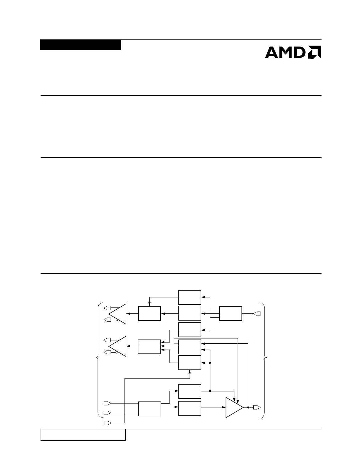
GENERAL DESCRIPTION
The Am7996 IEEE 802.3/Ethernet/Cheapernet Transceiver supports Ethernet Version 2, IEEE 802.3
10BASE-5 and IEEE 802.3 10BASE-2—Cheapernet)
transceiver applications. Transmit, receive, and collision detect functions at the coaxial media interface to
the data terminal equipment (DTE) are all performed by
this single device.
In an IEEE 802.3 (10BASE-5)/Ethernet application, the
Am7996 interfaces the coaxial (0.4 ″ diameter) media to the
DTE through an isolating pulse transformer and the 78 Ω
attachment unit interface (AUI) cable. In IEEE 802.3
10BASE-2—Cheapernet applications, the Am7996 typically resides inside the DTE with its signals to the DTE isolated and the coaxial (0.2 ″ diameter) media directly
Noise rejection filter ensures that only valid data
is transmitted onto the network
Collision detection on both transmit and receive
data
Collision detect threshold levels adjustable for
other networking applications
connected to the DTE. Transceiver power and ground in
both applications are isolated from that of the DTE.
The Am7996’s tap driver provides controlled skew and
current drive for data signaling onto the media. The jabber
controller prevents the node from transmitting excessively. While transmitting, collisions on the media are detected if one or more additional stations are transmitting.
The Am7996 features an optional SQE Test function
that provides a signal on the Cl pair at the end of every
transmission. The SQE Test indicates the operational
status of the Cl pair to the DTE. It can also serve as an
acknowledgment to the node that packet transmission
onto the coax was completed.
BLOCK DIAGRAM
DI+
DI–
CI+
CI–
AUI Interface
DO+
DO–
SQE TEST
Publication# 07506 Rev: EAmendment/0
Issue Date: May 1994
Line
Driver
Line
Driver
Control
Logic
Control
Logic
Input
Buffer
Carrier
Detect
Circuit
Receive
Data
Amplifier
Collision
Detect
Circuit
Jabber
Timer
SQE Test
Generator
Transmit
Squelch
Transmit
Data
Amplifier
Input
Buffer
Tap
Driver
RXT
Coaxial Media Interface
TXT
07506E-1
1
AMD
RELATED PRODUCTS
Part No. Description
Am79C98 Twisted Pair Ethernet Transceiver (TPEX)
Am79C100 Twisted Pair Ethernet Transceiver Plus (TPEX+)
Am79C981 Integrated Multiport Repeater Plus (IMR+)
Am79C987 Hardware Implemented Management Information Base (HIMIB)
Am79C940 Media Access Controller for Ethernet (MACE)
Am79C90 CMOS Local Area Network Controller for Ethernet (C-LANCE)
Am79C900 Integrated Local Area Communications Controller (ILACC)
Am79C960 PCnet-ISA Single-Chip Ethernet Controller (for ISA bus)
Am79C961 PCnet-ISA
+
Single-Chip Ethernet Controller (with Microsoft Plug n’ Play Support)
Am79C965 PCnet-32 Single-Chip 32-Bit Ethernet Controller (for 386DX, 486 and VL buses)
Am79C970 PCnet-PCI Single-Chip Ethernet Controller (for PCI bus)
Am79C974 PCnet-SCSI Combination Ethernet and SCSI Controller for PCI Systems
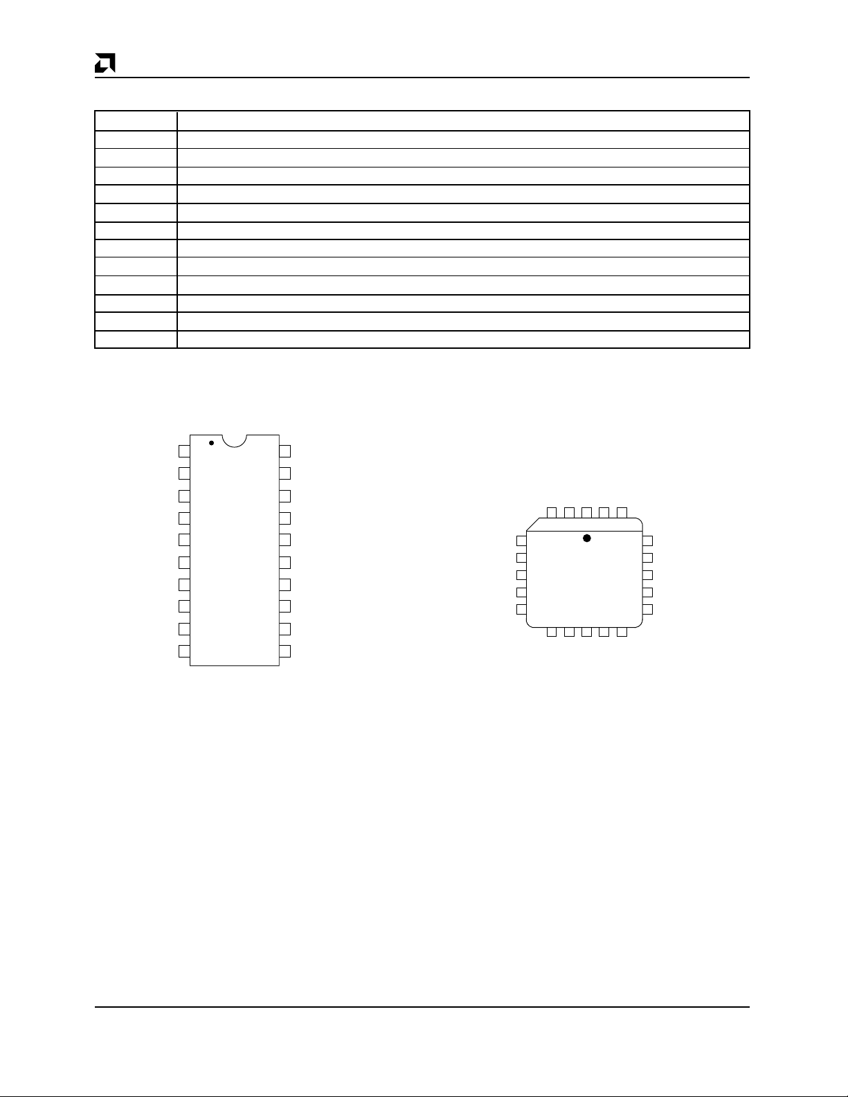
CONNECTION DIAGRAMS
DIP PLCC
V
CI+
CI–
DI+
DI–
V
C
SQE^TEST
DO+
DO–
V
Notes:
Pin 1 is marked for orientation.
NC = No Connection
CC1
REF
1
2
3
4
5
6
7
8
9
10
EE
20
19
18
17
16
15
14
13
12
11
V
CC2
COLL OSC
V
COL
NC
RXT
NC
TAP SHIELD
V
TX–
TXT
V
TX+
07506E-2
DI+
DI–
VC
REF
SQE^TEST
DO+
CI+
CI–
3212019
4
5
6
7
8
91011
EE
V
DO–
CC1
V
1213
TX+
V
CC2
V
COLL OSC
18
17
16
15
14
TX–
V
TXT
V
COL
NC
RXT
NC
TAP SHIELD
07506E-3
2 Am7996
ORDERING INFORMATION
Standard Products
AMD standard products are available in several packages and operating ranges. The order number (valid combination) is formed
by a combination of the elements below.
AM7996 D C
DEVICE NUMBER/DESCRIPTION
Am7996
IEEE 802.3/Ethernet/CheapernetTransceiver
B
OPTIONAL PROCESSING
Blank=Standard Processing
B=Burn-In
TR=Tape and Reel Packaging
OPERATING CONDITIONS
C = Commercial (0°C to +70°C)
PACKAGE TYPE
P=20-Pin Plastic DIP (PD 020)
D=20-Pin Ceramic DIP (CD 020)
J=20-Pin Plastic Leaded Chip Carrier (PL 020)
SPEED
Not Applicable
AM7996
Valid Combinations
PC, PCB, DC, DCB,
JC, JCTR
Valid Combinations
Valid combinations list configurations planned to be supported in volume for this device. Consult the local AMD sales
office to confirm availability of specific valid combinations and
to check on newly released combinations.
Am7996 3
PIN DESCRIPTION
Attachment Unit Interface (AUI)
Dl+, Dl–
Receive Line Output (Differential Outputs)
This pair is intended to operate into terminated 78 Ω
transmission lines. Signals at RXT meeting bandwidth
requirements and carrier sense levels are outputted at
Dl ± . Signaling at Dl ± meets requirements of
IEEE 802.3, Rev. D.
Cl+, Cl–
Collision Line Output (Differential Outputs)
This pair is intended to operate into terminated 78 Ω
transmission lines. Signal Quality Error (SQE), detected at DO ± inputs (excessive transmissions) or RXT
input (during a collision), outputs the 10 MHz internal
oscillator signal to the AUI interface. For proper component values at COLL OSC, signaling at Cl ± meets requirements of IEEE 802.3, Rev. D.
DO+, DO–
Transmit Input (Differential Inputs)
A pair of internally biased line receivers consisting of a
squelch detect receiver with offset and noise filtering
and a data receiver with zero offset for data signal processing. Signals meeting squelch requirements are
waveshaped and output at TXT.
Coaxial Media Interface (TAP)
RXT
Media Signal Receiver Input (Input)
RXT connects to the media through a 4:1 attenuator of
100 k Ω total resistance (25 k Ω and 75 k Ω in series).
Return for the attenuator is V
. RXT is an analog
COL
input with internal AC coupling for Manchester data signals and direct coupling for Carrier Detect and SQE average level detection. Signals at RXT meeting carrier
squelch enable data to the Dl ± outputs. Data signals
are AC coupled to Dl ± with a 150 ns time constant,
high-pass filter. Signals meeting SQE levels enable
COLL OSC frequency to Cl ± outputs.
TXT
Tap Node Driver (Input/Output)
A controlled bandwidth current source and sense amplifier. This l/O port is to be connected to the media
through an isolation network and a low-pass filter. Signals meeting DO ± squelch and jabber timing requirements are output at TXT as a controlled rise and fall
time current pulse. When operated into a double terminated 50 Ω transmission line, signaling meets
IEEE 802.3, Rev. D recommendations for amplitude,
pulse-width distortion, rise and fall times, and harmonic
content. The sense amplifier monitors TXT faults and
inhibits transmission.
Global Signals
VC
REF
Timing Reference Set (Input)
VC
is a compensated voltage reference input with
REF
respect to V
VC
and V
REF
. When a resistor is connected between
EE
, then internal transmit and receive
EE
squelch timing, SQE oscillator frequency, and receive
and SQE output drive levels are set. SQE frequency
set is also determined by components connected between V
SQE
and COLL OSC.
CC1
TEST
Signal Quality Error Test Enable (Input)
The SQE Test function is enabled by connecting the
TEST pin to V
SQE
V
TX+
, V
TX–
and disabled by connecting to V
EE
CC
Tap Node Driver Current Set (Inputs)
A reference input for transmission level and external redundant jabber. Transmit level is set by an external resistor between V
R = 9.09 Ω ). V
V
+ 1 V. When the voltage at V
EE
than V
+ 2 V, TXT is disabled and an SQE message
EE
and V
TX+
may be operated between V
TX–
(for an 80 mA peak level,
TX–
goes more positive
TX–
EE
and
is output at the Cl pair.
TAP SHIELD
Low-Noise Media Cable Return (Input)
This input is the return for V
reference and the re-
COL
ceive signal from the media. External connection is to
a positive power supply.
V
COL
SQE Reference Voltage (Bias Supply)
SQE sense voltage and RXT input amplifier reference.
An internally set analog reference for SQE level and data
signal set at –1.600 V nominal with a source resistance
of 150 Ω nominal. This reference should be filtered with
respect to TAP SHIELD (see Applications section for adjusting threshold levels for other applications).
COLL OSC
SQE Timing Set (Input)
Timing input for SQE oscillator. For a properly set input
at VC
10 MHz SQE oscillator frequency, R should be 1 k Ω and
C 47 pF, including interconnect and device capacitance.
V
Positive Logic Supply
V
SQE Timing Reference (Positive Supply Voltage)
Timing reference return for SQE oscillator and analog
signal ground.
V
Negative Logic Supply and IC Substrate
, SQE oscillator period is set at 2.1RC. For a
REF
CC1
CC2
EE
.
4 Am7996

FUNCTIONAL DESCRIPTION
The Am7996 IEEE 802.3/Ethernet/Cheapernet Transceiver consists of four sections: 1) Transmit—receives
signals from DTE and sends it to the coaxial medium;
2) Receive—obtains data from media and sends it to
DTE; 3) Collision Detect—indicates to DTE any collision on the media; and 4) Jabber—guards medium
from node transmissions that are excessive in length.
Transmit
The Am7996 receives differential signals from the DTE
(in the case of Am7990 family applications, from the
Am7992—serial interface adapter—SIA). For IEEE
(10BASE-5)/Ethernet applications, this signal is received through the AUI cable and isolation transformer.
In IEEE 802.3 10BASE-2—Cheapernet applications,
the AUI cable is optional.
Data is received through a noise rejection filter that rejects signals with pulse widths less than 7 ns (negative
going), or with levels less than 175 mV peak. Only signals greater than –275 mV peak from the DTE are enabled. This minimizes false starts due to noise and
ensures that no valid packets are missed.
The Am7996’s tap driver provides the driving capability
to ensure adequate signal level at the end of the maximum length network segment (500 meters) under the
worst-case number of connections (100 nodes). Required rise and fall times of data transmitted on the network are maintained by the Am7996 Tap Driver. The tap
driver’s output is connected to the media through external isolating diodes. To safeguard network integrity, the
driver is disabled whenever power falls below the minimum operation voltage.
During transmission, the Am7996 Jabber Controller
monitors the duration that the transmit tap driver is active and disables the driver if the jabber time is exceeded. This prevents network tie-up due to a
“babbling” transceiver. Once disabled, the driver is not
reset until 400 ms after the DO pair is idle and there is
no fault on TXT. During the disable time, an SQE signal
is sent on the Cl pair to the DTE.
When SQE
an SQE message at the end of every transmission. This
signal is a self-test indication to the DTE that the media
attachment unit (MAU) collision pair is operational.
TEST is tied to V
, the Am7996 generates
EE
Receive and Carrier Detect
Signal is acquired from the tap through a highimpedance (100 k Ω ) resistive divider. A high inputimpedance (low capacitance, high bandwidth, low
noise) DC-coupled input amplifier in the Am7996 receives the signal. The received signal passes through
a high-pass filter to minimize inter-symbol distortion,
and then through a data slicer. The Am7996 Carrier
Detect compares received signals to a reference.
Signals meeting carrier squelch requirements enable
data to the differential line driver within five bit times
from the start of the packet.
Received data is transmitted from the Dl pair through
an isolation transformer to the AUI cable (Ethernet/
lEEE 802.3—10BASE-5). In IEEE 802.3 10BASE-2—
Cheapernet, the AUI cable is optional. Following the
last transition of the packet, the Dl pair is held HIGH for
two bit times and then decreases to idle level within
twenty bit times.
Collision Detect
The Am7996 detects collisions on transmit if one or
more additional stations are transmitting on the network.
Received signals are compared against the collision
threshold reference. If the level is more negative than
the reference, an enable signal is generated to the Cl
pair. The collision threshold can be modified by
external components.
The collision oscillator is a 10 MHz oscillator that drives
the differential Cl pair to the DTE through an isolation
transformer.
This signal is gated to the Cl pair whenever there is a
collision, the SQE Test is in progress, or the jabber controller is activated. The oscillator is also utilized in
counting time for the jabber timer and SQE Test.
The Cl ± output meets the drive requirements for the
AUI interface. The output stays HIGH for two bit times
at the end of the packet, decreasing to the idle level
within twenty bit times.
Jabber Function
The Am7996 Jabber Timer monitors the activity on the
DO pair and senses TXT faults. It inhibits transmission
if the tap driver is active for longer than the jabber time
(26 ms). An SQE message (10 MHz collision signal), is
enabled on the Cl pair for the fault duration.
After the fault is removed, the jabber timer counts the
unjab time of 400 ms before it enables the driver.
If desired, a redundant jabber function can be implemented externally, and the output driver disabled by removing the driver supply at V
this condition and forces an SQE message on the Cl
pair during the disable time.
.The Am7996 senses
TX–
SQE Test
An SQE Test will occur at the end of every transmission
if the SQE
is a gated 10 MHz signal to the Cl pair. The SQE Test ensures that the twisted-pair assigned for collision notification to the DTE is intact and operational. The SQE Test
starts eight bit times after the last transition of the transmitted signal and lasts for a duration of eight bit times.
The SQE Test can be disabled by connecting the
SQE
TEST pin is tied to V
TEST pin to V
CC
. The SQE Test signal
EE
.
Am7996 5
AMD
APPLICATIONS
The Am7996 is compatible with Ethernet Version 2 and
IEEE 802.3 10BASE5 and 10BASE2 applications. (See
Figure 1).
MAU
Ethernet
Local
CPU
AUI - Attachment Unit Interface
DTE - Data Terminal Equipment
MAU - Media Access Unit
Cheapernet
Local
CPU
Local
Memory
Local Bus
Local
Memory
Local Bus
Am7990
LANCE
Am7990
LANCE
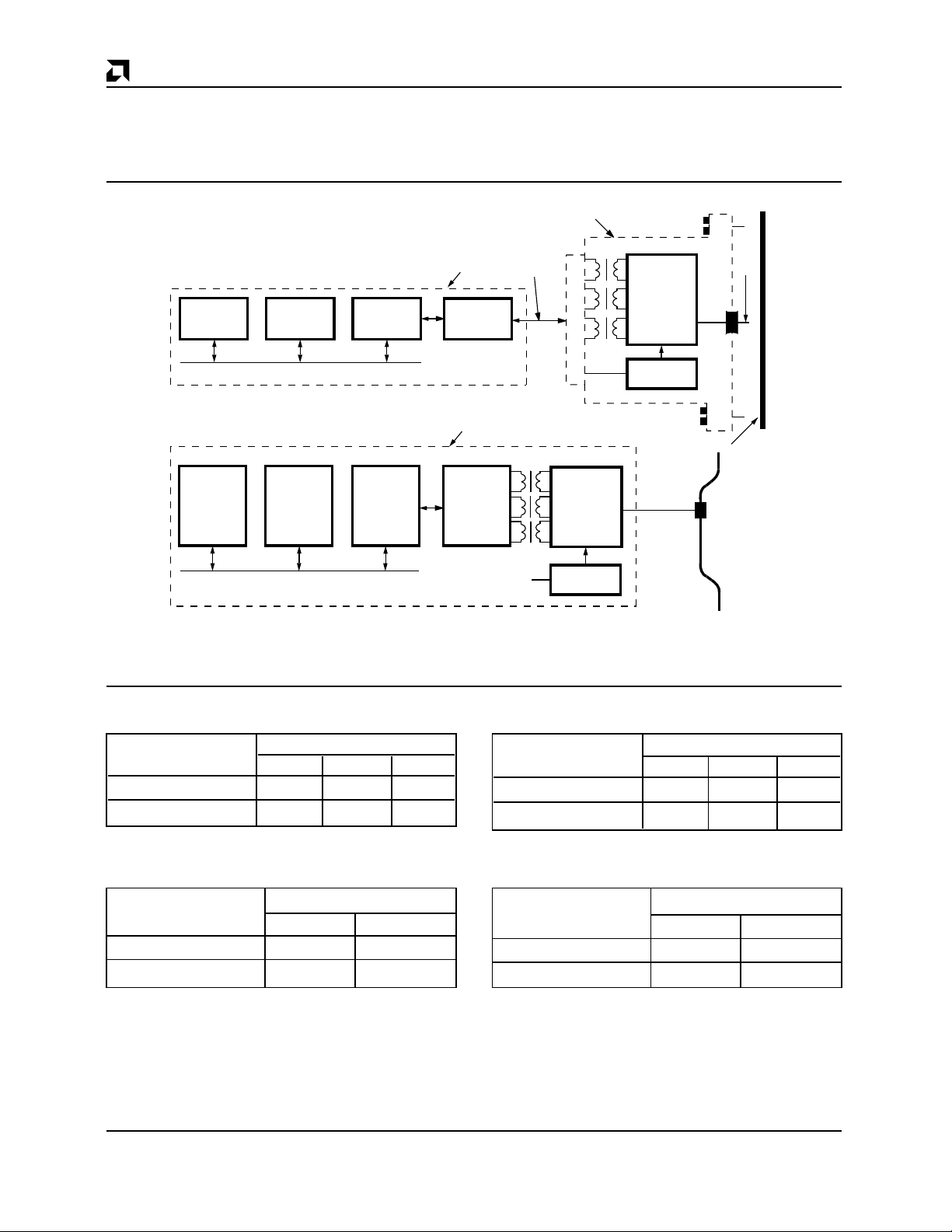
Figure 1. Typical Ethernet Node
Table 1. Transmit Mode Collision Detect
Function Table
MAU
Mode of Operation < 2 = 2 > 2
Transmitting No Yes Yes
Not Transmitting No May Yes
Number of Transmitters
DTE
Am7992B
SIA
DTE
Am7992B
SIA
AUI
Cable
Am7996
Transceiver
Power
Supply
Am7996
Transceiver
Power
Supply
Table 3. Receive Mode Collision Detect
Function Table
MAU
Mode of Operation < 2 = 2 > 2
Transmitting No Yes Yes
Not Transmitting No Yes Yes
Number of Transmitters
Tap
Ethernet
Coax
RG58
BNC "T"
07506E-4
Table 2. IEEE 802.3 Recommended Transmit
Mode Collision Detect Thresholds
Threshold Voltage Level
IEEE 802.3
No Detect Must Detect
10BASE5, Ethernet –1.492 V –
10BASE2, Cheapernet –1.404 V –1.782 V
6 Am7996
Table 4. IEEE 802.3 Recommended Receive
Mode Collision Detect Thresholds
Threshold Voltage Level
IEEE 802.3
10BASE5, Ethernet –1.492 V –1.629 V
10BASE2, Cheapernet –1.404 V –1.581 V
No Detect Must Detect

AMD
Figure 2 is an external component diagram showing
how to implement the transmit mode collision detect
levels recommended by IEEE 802.3. Figure 3 on the
following page shows how to implement the receive
mode collision detect levels recommended by
IEEE 802.3. Receive mode collision detect threshold
PE64102/PE64107 (or equivalent)
(75 µH)
COLL
RCV
XMT
1:1
1:1
1:1
R1
40.2 Ω
1%
R2
40.2 Ω
1%
1
2
3
4
5
R3
174 Ω
6
1%
7
(Note 3)
8
9
10
V
CC1
CI+
CI–
DI+
DI–
VC
SQE^TEST
DO+
DO–
V
EE
levels of the Am7996 are implemented by adding R9,
R10 and C4. For the values of the components shown in
Figure 3, a nominal receive mode collision detect
threshold of –1.5 V, for a –1.404 V to –1.581 V window,
is achieved.
C2
0.1 µF
R6
24.9 kΩ
1%
1N4001
D3
R7
9.09 Ω
1%
COLL OSC
Am7996
REF
V
CC2
V
COL
RXT
Tap
Shield
V
TX-
TXT
V
TX+
NC
NC
R4
1%
20
19
18
17
16
15
14
13
12
11
1.1 kΩ
(Note 5)
R8
9.09 Ω
1%
180 pF
C1
39 pF
(Note 6)
C
L
(Note 1)
C3
Coax
Connector
R5
75 kΩ
1%
C
C
(Note 2)
D2
(Note 1)
D1
1N4150
Power (DTE)
MAU Power Supply
(Note 4)
–9 V
GND
Notes:
is the effective load capacitance across R6; CC is the compensation capacitance (CC = 1/3 CL).
1. C
L
2. D2 can be eliminated in Cheapernet (IEEE 802.3, 10BASE2) applications.
3. Shown with SQE Test disabled.
4. Discrete Power Supply or Hybrid-Hybrid DC-DC Converter Manufacturers include:
Ethernet (IEEE 802.3, 10BASE5)
Reliability: 2E12R9
Valor Electronics: PM1001
Cheapernet (IEEE 802.3, 10BASE2)
Reliability Inc: 2VP5U9
Valor Electronics: PM7102
5. The capacitance of C3, Am7996 package, D3 and the printed circuit board should add up to 180 pF
±
6. The capacitance of C1, Am7996 package and the printed circuit board should add up to 39 pF.
7. Figure 2 used for production testing of all parameters that are tested.
Figure 2. Am7996 External Component Diagram for Transmit Mode Collision Detect
07506E-5
20%.
7Am7996

AMD
PE64102/PE64107 (or equivalent)
(75 µH)
COLL
RCV
XMT
Notes:
1:1
1:1
1:1
Power (DTE)
R1
40.2 Ω
1%
R2
40.2 Ω
1%
MAU Power Supply
(Note 4)
–9 V
GND
1
2
3
4
5
R3
174 Ω
6
1%
7
(Note 3)
8
9
10
V
CC1
CI+
COLL OSC
CI–
DI+
Am7996
DI–
VC
REF
SQE^TEST
DO+
DO–
V
EE
V
CC2
V
COL
NC
RXT
NC
Tap
Shield
V
TX–
TXT
V
TX+
C2
0.1 µF
R6
24.9 kΩ
1%
1N4001
D3
R7
9.09 Ω
1%
C1
39 pF
(Note 6)
C
L
(Note 1)
C3
(Note 5)
R4
1%
C4 0.1 µF
R9
499 Ω
1%
1.1 kΩ
(Note 7)
150 kΩ
9.09 Ω
1%
R10
1%
180 pF
20
19
18
17
16
15
14
13
12
11
Coax
Connector
R5
75 kΩ
1%
C
C
(Note 2)
D2
(Note 1)
D1
1N4150
07506E-6
is the effective load capacitance across R6; CC is the compensation capacitance (CC = 1/3 CL).
1. C
L
2. D2 can be eliminated in Cheapernet (IEEE 802.3, 10BASE2) applications.
3. Shown with SQE Test disabled.
4. Discrete Power Supply or Hybrid-Hybrid DC-DC Converter Manufacturers include:
Ethernet (IEEE 802.3, 10BASE5)
Reliability: 2E12R9
Valor Electronics: PM1001
Cheapernet (IEEE 802.3, 10BASE2)
Reliability Inc: 2VP5U9
Valor Electronics: PM7102
5. The capacitance of C3, Am7996 package, D3 and the printed circuit board should add up to 180 pF
±
6. The capacitance of C1, Am7996 package and the printed circuit board should add up to 39 pF.
7. R9, R10 and C4 are for Receive Mode Collision detection only.
Figure 3. Am7996 External Component Diagram with Collision Threshold Modified
for Receive Mode Collision Detect
20%.
8 Am7996

AMD
LAYOUT CONSIDERATIONS
To protect the transceiver from the environment and to
achieve optimum performance, the Am7996 is designed
to be used with two sets of external components: the
transmitter circuit consisting of components D1, D2, D3,
R7, R8, and C3, and the receiver circuit consisting of
components R5, R6, C
pacitance rather than a discrete component). These two
circuits are shown in both Figure 2 and in Figure 3 respectively. The resistor tolerances for these circuits are
specified as 1% for temperature stability.
The only layout restriction for the transmitter circuit is
that the longest current path from the TXT pin (Pin 12) to
the coaxial cable’s center conductor must be no longer
than 4 inches.
The layout of the receiver circuit, however, is critical. To
minimize parasitic capacitance that can degrade the received signal, the external receiver circuit should be isolated from power and ground planes. There must be no
power or ground plane under the area of the PC board
that includes pins 15 through 20, R5, R6, and the connector for the coaxial cable. If a power or ground plane
extends under this area, the receiver will not function
properly due to excessive crosstalk and under- or overcompensation of the R5, R6 attenuator. Also, the RXT
pin (Pin 16) should be as close to the coaxial cable
connector as possible.
Since there are no severe layout restrictions on the
transmitter circuit, the layout can be simplified by omitting power and ground planes from the whole area on
the right side of the Am7996 as shown in Figure 4-1.
, and CC, (CL is a parasitic ca-
L
If the above layout rules are followed, the parasitic
capacitance in parallel with R6 will be about 6 pF. This
parasitic capacitance is shown in the schematics as C
(Note that CL is a parasitic capacitance. Do not add a
discrete capacitor in parallel with R6). The capacitor
labeled C
in the schematics is the total capacitance in
C
parallel with R5 including parasitic capacitance. The
parasitic component of C
mum performance, the ratio of C
will be about 1 pF. For opti-
C
to CC should be the
L
same as the ration of R5 to R6, which is 3 to 1. This
means that an additional 1 pF of capacitance must be
added in parallel with R5.
This additional capacitance can easily be added by
building a parallel-plate capacitor for PC traces right under resistor R5. This capacitor can consist of a 0.200 in.
by 0.200 in. square of conductor on each side of the
board as shown in Figure 4-2 (These dimensions assume that the PC board is made from 0.060 in. thick
G-10 material). The top plate of the capacitor should be
connected to one lead of R5, and the bottom plate
should be connected to the other lead. Figure 4-3 shows
an example of this suggested layout for a four layer
printed circuit board. Note that the component labeling
used in Figure 4-3 is not intended to correspond with the
component labeling used in Figure 2 and Figure 3.
R5
L
20
RXT
Am7996
TXT
11
R5, R6, R4
C1, C2
D1, D2, D3
R7, R8
C3
Area with no power or ground plane
Connector
Figure 4-1.
Coax
07506E-7
Component
Side
Circuit
Side
0.200 in x 0.200 in
two planes
07506E-8
Figure 4-2.
9Am7996


AMD
ABSOLUTE MAXIMUM RATINGS
Storage Temperature –65°C to +150°C. . . . . . . . . . .
Ambient Temperature
Under Bias 0°C to +70°C. . . . . . . . . . . . . . . . . . . . . .
, V
Supply Voltages (V
EE
DC Input Voltage (D0+, D0–) –12.0 V to +0.5 V. . . .
DC Input Voltage (RXT) –6 V to +0.5 V. . . . . . . . . . .
Stresses above those listed under Absolute Maximum Ratings may cause permanent device failure. Functionality at or
above these limits is not implied Exposure to absolute maximum ratings for extended periods may affect device reliability.
) –12.0 V to +0.5 V. . . . .
TX–
OPERATING RANGES
Commercial (C) Devices
Ambient Temperature (T
Supply Voltage (V
Operating ranges define those limits between which the functionality of the device is guaranteed
EE
)0°C to +70°C. . . . . . .
A
) –8.1 V to –9.9 V. . . . . . . . . .
11Am7996

AMD
DC CHARACTERISTICS over operating ranges unless otherwise specified
Parameter
Symbol Parameter Description Test Conditions (Note 10) Min Typ Max Unit
Transmit Signals
V
TXTH
V
TXTL
V
TXT
Transmit Output HIGH Voltage (Note 1) RLX = 25 Ω 0 –0.05 –0.425 V
Transmit Output LOW Voltage (Note 1) RLX = 25 Ω –1.625 –2.0 –2.2 V
Transmit Average DC Voltage with 50% RLX = 25 Ω –0.925 –1.0 –1.1 V
Duty-Cycle into DO+, DO– (Note 1)
V
ICM
DO+, DO– Common Mode Bias IIN = 0 V
Voltage + 1.2 + 1.5 + 1.8
V
IDC
Differential Input Squelch Threshold –175 –225 –275 mV
(DO+, DO–) (Note 9)
I
TXTL
I
ILD VIN
I
IHD VIN
R
IDF
R
ICM
Transmit Current (Note 9) V
= –5.5 V –65 –88 mA
TXT
= VEE Max –2.0
Input Current (DO+, DO–)
VEE = Max
= 0 2.5
Differential Input Resistance (DO+, DO–) VIN = 0 to VEE 68 kΩ
Common-Mode Input Resistance (DO+, DO–)VIN = 0 to VEE 1.5 2 kΩ
Receive/Collision Signals
V
OD
V
CMT
Differential Output Voltage V
(DI+, DI–; CI+, CI–) V
R
= 78 Ω
L
Common-Mode Output R
OD+
OD–
= 78 Ω –1.0 –2.0 –3.0 V
L
(DI+, DI–; CI+, CI–)
V
ODI
V
OFF Differential Output Idle Voltage RL = 78 Ω, VEE = Max –20 0 +20 mV
OD
Differential Output Voltage Imbalance R
(DI+, DI–; CI+, CI–) ||V
| – |VOD|| (Note 6)
OD
= 78 Ω 520mV
L
(DI+, DI–; CI+, CI–)
V
CAT
V
COT
I
RXT
I
OFF Differential Output Idle Current RL = 0 –0.5 0 +0.5 mA
OD
Carrier Sense Threshold VIN = 5 MHz Preamble –400 –500 –600 mV
Collision Sense Threshold (Note 5) –1515–1600 –1700 mV
RXT Input Bias Current VIN = 1 V to –2.5 V; –0.5 0 +0.5 µA
= Max
V
EE
(DI+, DI–; CI+, CI–)
Global
I
EE
Supply Current–Non-Transmitting –88 –105
Supply Current–Transmitting –128 –155
RLX = 25 Ω (Note 4)
Commercial
EE VEE
V
EE
+550 +670 +850
–550 –670 –850
V
mA
mV
mA
CAPACITANCE* (TA = 25°C; VEE = 0; Pins 15, 17—No Connections)
Parameter
Symbol Parameter Description Test Conditions Min Typ Max Unit
C
RXT
RXT Input Capacitance pF
Notes:
See notes following Switching Characteristics section.
*Parameters are not “Tested.”
12 Am7996
Ceramic DIP 1.7
Plastic DIP/PLCC 1.1

AMD
SWITCHING CHARACTERISTICS over operating ranges unless otherwise specified
Parameter
No Symbol Parameter Description Test Conditions Min Typ Max Unit
Receiver Specification
1t
2t
3t
4t
5t
7t
PWREJ
PWTON
PWSON
PWOFF
TON
TSD
DO± Input Pulse Width to Reject
(DO± ≥ V
, Max) (Note 1) 15 7 ns
IDC
DO± Input Pulse Width to Turn On
(DO± > V
, Max) (Note 1) 20 15 ns
IDC
DO± Input Pulse Width to Stay On
(DO± ≥ V
, Max) (Note 1) 105 ns
IDC
DO± Input Pulse Width to Turn Off
(DO± ≥ V
, Max) (Note 1) 160 ns
IDC
Transmit Driver Turn-On Delay (Note 1) 200 ns
Transmit Static Delay (Zero Crossing
to 50% Point to Coax) (Note 1) 30 50 ns
8t
9t
10 t
11 t
TXTR
TXTF
DRF
SKEW
Transmit Driver Rise Time (Notes 1, 7) 20 25 30 ns
Transmit Driver Fall Time (Notes 1, 7) 20 25 30 ns
Difference in Driver Rise and Fall
Times |t
TXTR–tTXTF
| (Notes 1, 7) 1.0 ns
Output Driver Skew—Transmit Data
Symmetry (Note 1) –2.0 +2.0 ns
12 t
13 t
14 t
JCT
JRT
JREC
Jabber Control Time (Note 1) 20 26 35 ms
Jabber Reset Time (Note 1) 340 419 500 ms
Jabber Recovery Time (Note 1) 1.0 µs
Receive/Collision Specification
15 t
16 t
17 t
RON
ROFF
RSD
Receiver Turn-On Delay V
Receiver Turn-Off Delay V
tap
tap
> V
Max 250 500 ns
CAT
< V
Min 1000 ns
CAT
Receiver Static Delay 50% Point at RXT
at Zero Crossing
at DI± Outputs 50 ns
18 t
19 t
20 t
21 t
22 t
23 t
24 t
25 f
26 t
27 t
RS
RR
RF
CON
COFF
CL
CH
CI
STD
STL
Receive Data Symmetry –2 +2 %
DI± and CI± Rise Time 20%–80%,
= 78 Ω 7ns
R
L
DI± and CI± Fall Time 80%–20%,
R
= 78 Ω 7ns
L
CI± Turn-On Delay V
CI± Turn-Off Delay V
tap
tap
> V
Max 900 ns
COT
< V
Min 2000 ns
COT
CI± LOW Time 35 50 70.5 ns
CI± HIGH Time 35 50 70.5 ns
Collision Frequency (Note 8) 8.5 10.0 11.5 MHz
SQE Test Delay Time FCI = 10.0 MHz 600 1000 ns
SQE Test Length FCI = 10.0 MHz 600 800 1000 ns
Commercial
13Am7996

AMD
Notes:
Ω
1. Parameters are measured at coax tap. In production test, parameters are measured across at 25
coax tap.
2. For conditions shown as Min or Max, use the appropriate value specified under Operating Range for the applicable
device type.
3. Typical values are at V
4. V
wired to VEE.
TX–
= –9.0 V, 25°C ambient.
EE
5. This threshold can be modified externally (see Figure 3).
6. Parameter not tested.
7. Tested on a 5 Mbps preamble (continuous 1010 pattern) measured between 20% and 80% points, test limits correlated to
10% and 90% data sheet limits shown.
8. Determined by Am7966 External Component Diagrams values for R4 and C1.
9. In production test, input signal applied thru transformer to DO
±
inputs.
10. Figure 2 used for production testing of all parameters.
*Notes listed correspond to the respective references made in DC Characteristics and Switching Characteristics tables.
load equivalent to the
14 Am7996

AMD
KEY TO SWITCHING WAVEFORMS
WAVEFORM INPUTS OUTPUTS
SWITCHING TEST CIRCUIT
DUT
Must be
Steady
May
Change
from H to L
May
Change
from L to H
Don’t Care,
Any Change
Permitted
Does Not
Apply
1/3 PE64102/PE64107 (or equivalent)
+
78 Ω
R
–
L
75 µH
Will be
Steady
Will be
Changing
from H to L
Will be
Changing
from L to H
Changing,
State
Unknown
Center
Line is HighImpedance
“Off” State
KS000010
A. AUI Transmit (DI+, DI–,; CI+, CI–)
RLX = 25 Ω
B. Test Load (TXT)
07506E-12
07506E-13
15Am7996

AMD
SWITCHING WAVEFORMS
DO±
V
IDC
COAX
TAP
(Transmit)
COAX
TAP
(Receive)
DI±
2
5
7
90%
10%
8
7
9
Transmit Function
NEAR END
V
CAT
max
50%
V
50%
CAT
min
0 V
V
TXTL
0 V
07506E-14
0 V
V
OD
0 V
–V
OD
15
17
17
Receiver Function
16 Am7996
17
17
16
07506E-15

AMD
SWITCHING WAVEFORMS
DO±
COAX
TAP
(Transmit)
CI±
*
SQE^TEST
pin connected to V
0 V
0 V
V
TXTL
V
OD
0 V
–V
OD
2726
07506E-16
SQE Test*
EE
DO±
COAX
TAP
(Transmit)
CI±
50%
12
Jabber Function
0 V
0 V
V
TXTL
50%
13
0 V
07506E-17
17Am7996

AMD
SWITCHING WAVEFORMS
V
80%
OD
DI±
CI±
CI±
23
1/f
0 V
20%
–V
OD
19
V
OD
20
0 V
–V
OD
24
CI
07506E-18
DI±/CI± Parameters
0 V
COAX
TAP
V
CI±
COT
MAX
–2 V
21
V
COT
22
MIN
350 mV
V
OD
0 V
–V
OD
07506E-19
Collision Detect Timing
Note:
This signal is used for test purposes. It represents the average value of the signal that might be seen on the coax tap when
a collision occurs.
18 Am7996
 Loading...