

Datasheet AM7992BPC, AM7992BJCTR, AM7992BJC, AM7992BDCB, AM7992BDC Datasheet (AMD Advanced Micro Devices)
Page 1
FINAL
Publication# 03378 Rev: I Amendment/0
Issue Date: May 1993
1
Am7992B
Serial Interface Adapter (SIA)
DISTINCTIVE CHARACTERISTICS
■
Compatible with lEEE 802.3/Ethernet/Cheapernet
specifications
■
Crystal/TTL oscillator-controlled Manchester
encoder
■
Manchester decoder acquires clock and data
within four bit times with an accuracy of ± 3 ns
■
Guaranteed carrier and collision detection
squelch threshold limits
—Carrier/collision detected for inputs greater than
–275 mV
—No carrier/collision for inputs less than –175 mV
■
Input signal conditioning rejects transient noise
—Transients <10 ns for collision detector inputs
—Transients <20 ns for carrier detector inputs
■
Receiver decodes Manchester data with worst
case ± 19 ns of clock jitter (at 10 MHz)
■
TTL-compatible host interface
■
Transmit accuracy +0.01% (without adjustments)
GENERAL DESCRIPTION
The Am7992B Serial Interface Adapter (SIA) is a
Manchester encoder/decoder compatible with IEEE
802.3, Cheapernet, and Ethernet specifications. In an
IEEE 802.3/Ethernet application, the Am7992B interfaces the Am7990 Local Area Network Controller for
Ethernet (LANCE) to the Ethernet transceiver device,
acquires clock and data within four bit times, and decodes Manchester data with worst case ± 19 ns phase
jitter at 10 MHz. SIA provides both guaranteed signal
threshold limits and transient noise suppression circuitry in both data and collision paths to minimize false
start conditions.
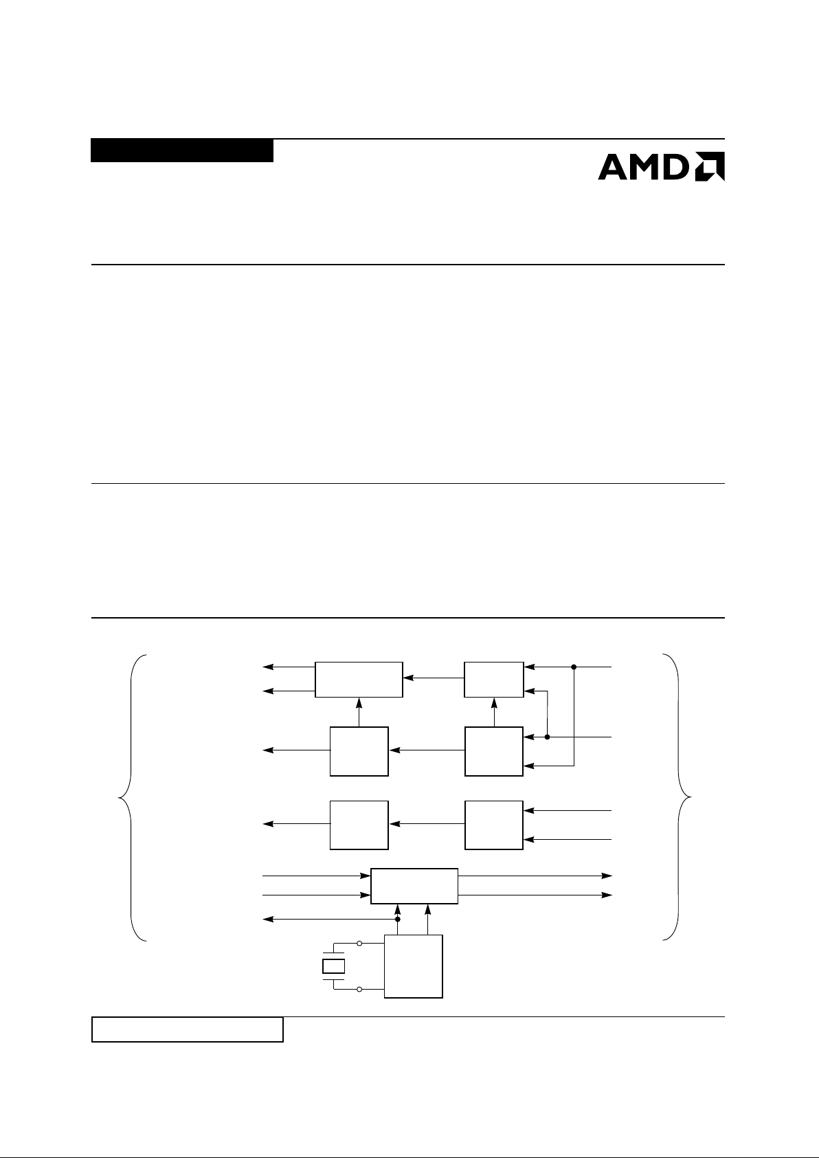
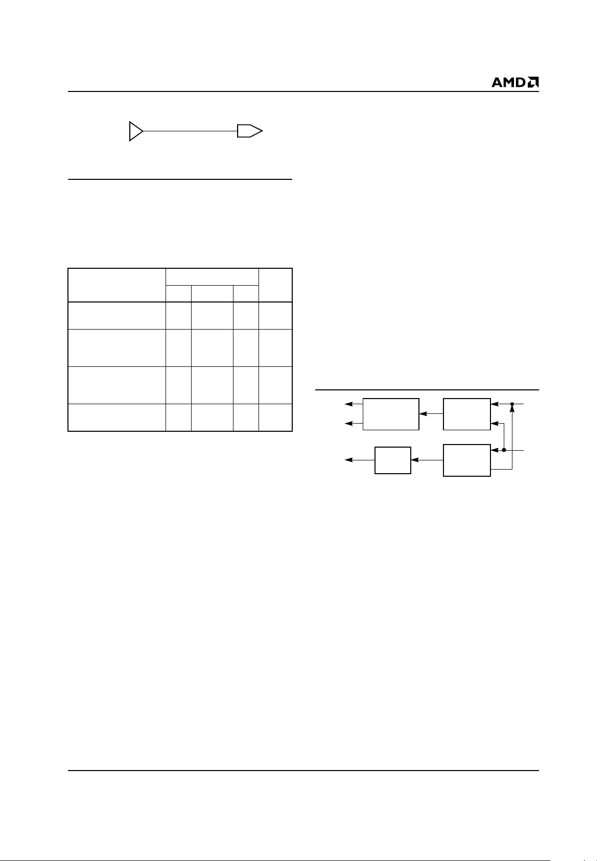
BLOCK DIAGRAM
03378I-1
Manchester
Decoder
Data
Receiver
Noise
Reject
Filter
Carrier
Detect
Noise
Reject
Filter
Collision
Detect
Manchester
Encoder
Crystal
OSC
Receive Data (RX)
Receive Clock (RCLK)
Carrier Present (RENA)
Collision (CLSN)
Transmit Data (TX)
Transmit Enable (TENA)
Transmit Clock (TCLK)
20 MHz
XTAL
1
XTAL
2
Receive+
Receive–
Collision+
Transmit+
Transmit–
Collision–
Controller Interface
Transceiver Interface
Page 2
AMD
2 Am7992B
RELATED PRODUCTS
Part No. Description
Am7990 Local Area Network Controller for Ethernet (LANCE)
Am7996 IEEE 802.3/Ethernet/Cheapernet/Transceiver
Am79C900 Integrated Local Area Communications Controller
TM
(ILACCTM)
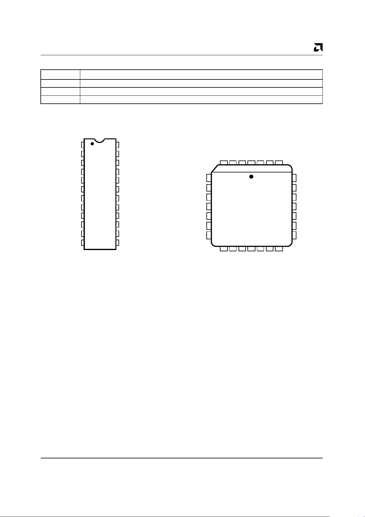
CONNECTION DIAGRAMS
Receive+
Collision–
DIP
CLSN
TCLK
Collision+
TEST
Transmit+
TX
GND1
RCLK
RX
Receive–
V
CC1
PF
TENA
1
3
5
7
9
11
12
10
2
4
8
6
24
22
20
18
16
14
13
15
23
21
17
19
RENA
TSEL
X1
GND2
RF
GND3
Transmit–
X2
V
CC2
Note:
Pin 1 is marked for orientation.
PLCC
03378I-2 03378I-3
1
234
2827
26
255
24
23
22
21
20
19
1817
1615
6
7
8
9
10
11
121314
RCLK
NC
TSEL
GND1
GND2
X1
X2
Receive-
TEST
V
CC1
NC
V
CC2
PF
RF
GND3
Transmit+
Transmit-
NC
TX
TCLK
TENA
NC
CLSN
RX
RENA
Colision+
Colision-
Receive+
Page 3
Am7992B 3
ORDERING INFORMATION
Standard Products
AMD standard products are available in several packages and operating ranges. The order number (valid combination) is formed
by a combination of the elements below.
Valid Combinations
Valid combinations list configurations planned to be supported in volume for this device. Consult the local AMD sales
office to confirm availability of specific valid combinations and
to check on newly released combinations.
AM7992B D C
DEVICE NUMBER/DESCRIPTION
Am7992B
Serial Interface Adapter
OPTIONAL PROCESSING
Blank=Standard Processing
B=Burn-In
OPERATING CONDITIONS
C = Commercial (0°C to +70°C)
PACKAGE TYPE
D=24-Pin (Slim) Ceramic DIP (CD3024)
J=28-Pin PLCC (PL 028)
P=24-Pin (Slim) Plastic DIP (PD3024)
SPEED
Not Applicable
B
Valid Combinations
AM7992B
DC, DCB, JC,
JCTR, PC
Page 4

4 Am7992B
PIN DESCRIPTION
CLSN
Collision (Output, TTL Active HIGH)
Signals at the Collision ±
terminals meeting threshold
and pulse-width requirements will produce a logic
HIGH at CLSN output. When no signal is present at
Collision ± , CLSN output will be LOW.
RX
Receive Data (Output)
A MOS/TTL output, recovered data. When there is no
signal at Receive ± and TEST
is HIGH, RX is HIGH. RX
is actuated with RCLK and remains active until RENA
is deasserted at the end of the message. During reception, RX is synchronous with RCLK and changes after
the rising edge of RCLK. When TEST
is LOW, RX is
enabled.
RENA
Receive Enable (Output, TTL Active HIGH)
When there is no signal at Receive+, RENA is LOW.
Signals meeting threshold and pulse-width “on” requirements will produce a logic HIGH at RENA. When
RENA is HIGH, Receive+ signals meeting threshold
and pulse-width “off” requirements will produce a LOW
at RENA.
RCLK
Receive Clock (Output)
A MOS/TTL output, recovered clock. When there is no
signal at Receive ± and TEST
is HIGH, RCLK is LOW.
RCLK is activated 1/4 bit time after the second negative
Manchester preamble clock transition at Receive ± and
remains active until after an end of message. When
TEST is LOW, RCLK is enabled and meets minimum
pulse-width specifications.
TX
Transmit (Input)
TTL-compatible input. When TENA is HIGH, signals at
TX meeting setup and hold time to TCLK will be
encoded as normal Manchester at Transmit+ and
Transmit–.
■
TX HIGH: Transmit+ is negative with respect to
Transmit– for first half of data bit cell.
■
TX LOW: Transmit+ is positive with respect to
Transmit– for first half of data bit cell.
TENA
Transmit Enable (Input)
TTL-compatible input. Active HIGH data encoder
enable. Signals meeting setup and hold time to TCLK
will allow encoding of Manchester data from TX to
Transmit+ and Transmit–.
TCLK
Transmit Clock (Output)
MOS/TTL output. TCLK provides symmetrical HIGH
and LOW clock signals at data rate for reference timing
of data to be encoded. It also provides clock signals for
the controller chip (Am7990—LANCE) and an internal
timing reference for receive path voltage-controlled
oscillators.
Transmit+, Transmit–
Transmit (Outputs)
A differential line output. This line pair is intended to operate into terminated transmission lines. For signals
meeting setup and hold time to TCLK at TENA and TX,
Manchester clock and data are outputted at Transmit+/
Transmit–. When operating into a 78 Ω terminated
transmission line, signaling meets the required output
levels and skew for both Ethernet and IEEE 802.3 drop
cables.
Receive+, Receive–
Receiver (Inputs)
A differential input. A pair of internally biased line receivers consisting of a carrier detect receiver with offset
threshold and noise filtering to detect the line activity,
and a data recovery receiver with no offset for
Manchester data decoding.
Collision+, Collision–
Collision (Inputs)
A differential input. An internally biased line receiver
input with offset threshold and noise filtering. Signals at
Collision ± have no effect on data-path functions.
TSEL
Transmit Mode Select (Output, Open Collector;
Input, Sense Amplifier)
■
TSEL LOW: Idle transmit state Transmit+ is positive
with respect to Transmit–.
■
TSEL HIGH: Idle transmit state Transmit+ and
Transmit– are equal, providing “zero” differential to
operate transformer-coupled loads.
When connected with an RC network, TSEL is held
LOW during transmission. At the end of transmission
the open collector output is disabled, allowing TSEL to
rise and provide a smooth transmission from logic
HIGH to “zero” differential idle. Delay and output return
to zero are externally controlled by the RC network at
TSEL and Transmit ± load inductance.
Page 5

Am7992B 5
X
1
, X
2
Biased Crystal Oscillator (Input)
X
1
is the input and X
2
is the bypass port. When connected for crystal operation, the system clock that appears at TCLK is half the frequency of the crystal
oscillator. X
1
may be driven from an external source of
two times the data rate.
RF
Frequency Setting Voltage-Controlled Oscillator
(V
CO
) Loop Filter (Output)
This loop filter output is a reference voltage for the receive path phase detector. It also is a reference for timing noise immunity circuits in the collision and receive
enable path. Nominal reference V
CO
gain is 1.25 TCLK
frequency MHz/V.
PF
Receive Path V
CO
Phase-Locked Loop Filter (Input)
This loop filter input is the control for receive path loop
damping. Frequency of the receive V
CO
is internally lim-
ited to transmit frequency ± 12%. Nominal receive V
CO
gain is 0.25 reference V
CO
gain MHz/V.
TEST
Test Control (Input)
A static input that is connected to V
CC
for Am7992B/
Am7990 operation and to ground for testing of
Receive ± path threshold and RCLK output HIGH
parameters. When TEST
is grounded, RX is enabled
and RCLK is enabled except during clock acquisition,
when RCLK is HIGH.
GND1
High Current Ground
GND2
Logic Ground
GND3
Voltage-Controlled Oscillator Ground
V
CC1
High Current and Logic Supply
V
CC2
Voltage-Controlled Oscillator Supply
Page 6
6 Am7992B
FUNCTIONAL DESCRIPTION
The Am7992B serial interface adapter (SIA) has three
basic functions. It is a Manchester encoder/line driver
in the transmit path, a Manchester decoder with noise
filtering and quick lock-on characteristics in the receive
path, and a signal detector/converter (10 MHz differential to TTL) in the collision path. In addition, the SIA provides the interface between the TTL logic environment
of the Local Area Network Controller for Ethernet
(LANCE) and the differential signaling environment in
the transceiver cable.
Transmit Path
The transmit section encodes separate clock and NRZ
data input signals meeting the setup and hold time to
TCLK at TENA and TX into a standard Manchester II
serial bit stream. The transmit outputs (Transmit+/
Transmit–) are designed to operate into terminated
transmission lines. When operating into a 78 Ω terminated transmission line, signaling meets the required
output levels and skew for IEEE 802.3/Ethernet/
Cheapernet.
Transmitter Timing and Operation
A 20 MHz fundamental mode crystal oscillator provides
the basic timing reference in the SIA. It is divided by two
to create the Transmit Clock reference (TCLK). Both
20 MHz and 10 MHz clocks are fed into the Manchester
Encoder to generate the transitions in the encoded
data stream. The 10 MHz clock, TCLK, is used by the
SIA to internally synchronize Transmit (TX) data and
Transmit Enable (TENA). TCLK is also used as a stable
bit rate clock by the receive section of the SIA and by
other devices in the system (the Am7990 LANCE uses
TCLK to drive its internal state machine). The oscillator
may use an external 0.005% crystal or an external
TTL-level input as a reference, which will achieve a
transmit accuracy of 0.01% (no external adjustments
are required).
Transmission is enabled when TENA is activated. As
long as TENA remains HIGH, signals at TX will be encoded as Manchester and will appear at Transmit+ and
Transmit–. When TENA goes LOW, the differential
transmit outputs go to one of two idle states determined
by the circuit configuration of TSEL:
TSEL HIGH: The idle state of Transmit ± yields “zero”
differential to operate transformer-coupled loads (see
Figure 2, Transmitter Timing—End of Transmission
waveform diagram and Typical Performance Curve
diagram).
TSEL LOW: In this idle state, Transmit+ is positive to
Transmit– (logical HIGH) (see figures and diagrams as
referenced above).
The End of Transmission—Return to Zero is determined by the external RX network at TSEL and by the
load at Transmit ± .
Manchester
Encoder
OSC
DO±
TX
TENA
TCLK
I
03378I-4
Figure 1. Transmit Section
VCC
680 pF
3K
C1
R2
20 pF
510
R1
C2
TSEL
PIN 5
A. TSEL LOW B. TSEL HIGH
TSEL
PIN 5
03378I-5 03378I-6
Figure 2. Transmit Mode Select (TSEL) Connection
Page 7
Am7992B 7
Figure 3. TTL Clock Driver Circuit for X
1
SIA Oscillator
Specification for External Crystal
When using a crystal to drive the Am7992B oscillator,
the following crystal specification should be used to ensure a transmit accuracy of 0.01%:
Some crystal manufacturers have generated crystals
to this specification. One such manufacturer is ReevesHoffman. Their ordering part number for this crystal is
RH#04-20423-312. Another manufacturer is Epson—
Part #MA 506-200M-50 pF, which is a surfacemounted crystal.
Specification for External TTL Level
When driving the oscillator from an external clock
source, X
2
must be left floating (unconnected). An
external clock having the following characteristics
must be used to ensure less than +0.5 ns jitter at
Transmit+ (see the X
1
Driven from External Source
waveform diagram and the TTL Clock Driver Circuit
for X1, Figure 3):
■Clock Frequency: 20 MHz ±0.01%
■Rise/Fall Time (tR/tF): <4 ns, monotonic
■X1 HIGH/LOW Time (t
HlGH/tLOW
): > 20 ns
■X1 Falling Edge-to-Falling Edge Jitter: < ±0.2 ns at
1.5 V input
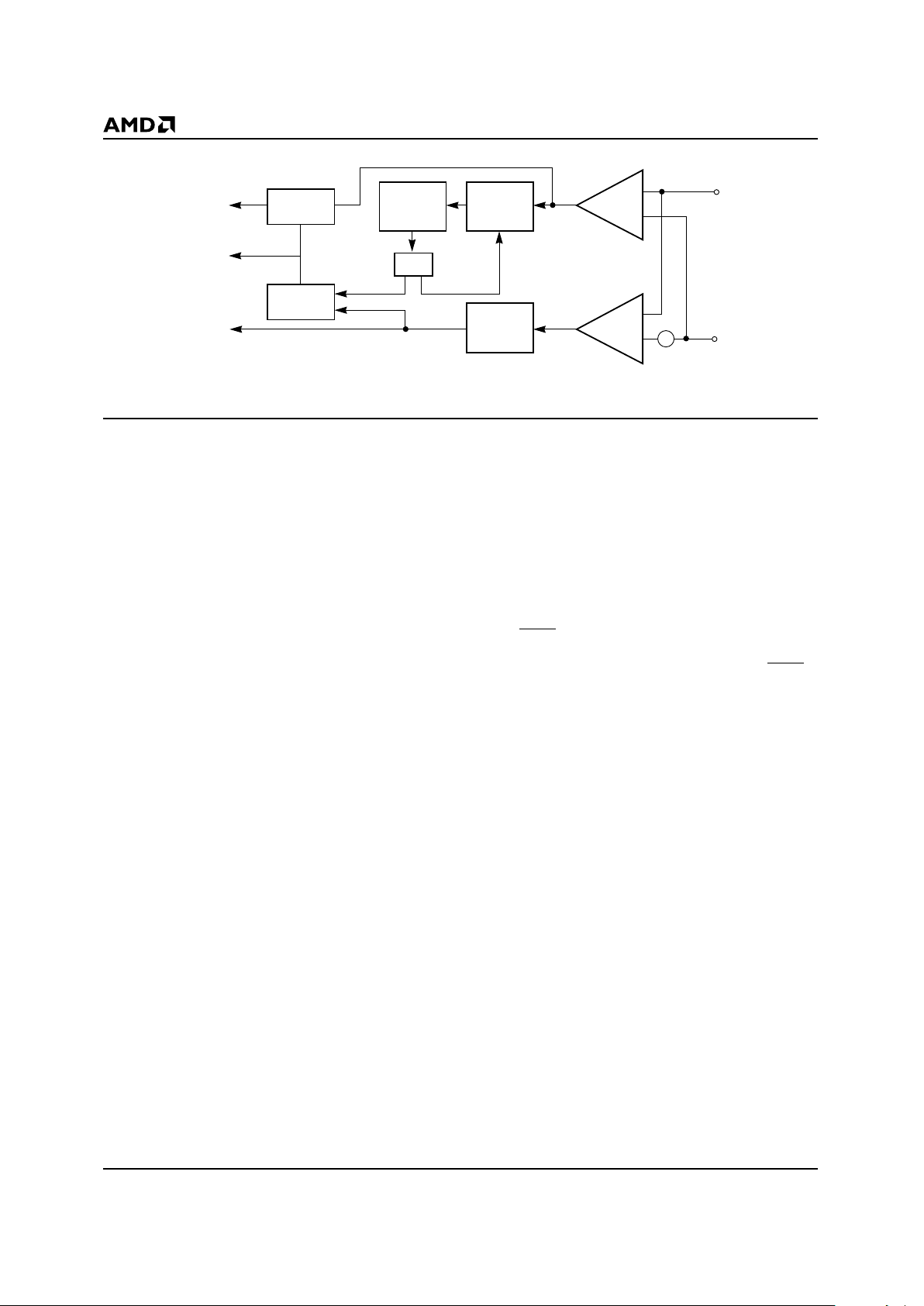
Receiver Path
The principle functions of the receiver are to signal the
LANCE that there is information on the receive pair and
to separate the incoming Manchester-encoded data
stream into clock and NRZ data.
The receiver section (see Figures 4 and 5) consists of
two parallel paths. The receive data path is a zero
threshold, wide bandwidth line receiver. The carrier
path is an offset threshold bandpass-detecting line receiver. Both receivers share common bias networks to
allow operation over an input common mode range of
0 V to 5.5V.
Limit
UnitMin Nominal Max
Resonant Frequency
Error with C
L
= 50 pF
–50 0 +50 PPM
Change in Resonant
Frequency Temperature
with C
L
= 50 pF
–40 +40 PPM
Parallel Resonant
Frequency with
C
L
= 50 pF
20 MHz
Motional Crystal
Capacitance, C
1
0.022 pF
X
1
ALS Driver or
Equivalent
03378I-7
Manchester
Decoder
Data
Receiver
Noise
Reject
Filter
Carrier
Detect
RX
RCLK
RENA
DI±
03378I-8
Figure 4. Receiver
Page 8
8 Am7992B
Input Signal Conditioning
The Carrier Receiver detects the presence of an incoming data packet by discerning and rejecting noise
from expected Manchester data. It also controls the
stop and start of the phase-locked loop during clock acquisition. In the Am7992B, clock acquisition requires a
valid Manchester bit pattern of 1010 to lock on the incoming message (see Receive Timing—Start of Reception Clock Acquisition waveform diagram).
Transient noise pulses less than 20 ns wide are rejected by the Carrier Receiver as noise and DC inputs
more positive than –175 mV are also suppressed. Carrier is detected for input signal wider than 45 ns with
amplitude more negative than –275 mV. When input
amplitude and pulse-width conditions are met at
Receive±, RENA is asserted and a clock acquisition
cycle is initiated.
Clock Acquisition
When there is no activity at Receive± (receiver is idle),
the receive oscillator is phase locked to TCLK. The first
negative clock transition (first valid Manchester “0”)
after RENA is asserted interrupts the receive oscillator
and presets the INTRCLK (internal clock) to the HIGH
state. The oscillator is then restarted at the second
Manchester “0” (bit time 4) and is phase locked to it. As
a result, the SIA acquires the clock from the incoming
Manchester bit stream in four bit times with a “1010”
Manchester bit pattern. The 10 MHz INTRCLK and
INTPLLCLK are derived from the internal oscillator,
which runs at four times the data rate (40.0 MHz). The
three clocks generated internally are utilized in the following manner:
■INTRCLK: After clock acquisition, INTRCLK
strobes the incoming data at 1/4 bit time. Receive
data path sets the input to the data decode register
(Figure 5).
■INTPLLCLK: At clock acquisition, INTPLLCLK is
phase locked to the incoming Manchester clock
transition at bit cell center (BCC). The transition at
BCC is compared to INTPLLCLK and phase correction is applied to maintain INTRCLK at 1/4 bit time
in the Manchester cell.
■INTCARR: From start to end of a message,
INTCARR is active and establishes RENA turn-off
synchronously with RCLK rising edge. Internal carrier goes active when there is a negative transition
that is more negative than –275 mV and has a pulse
width greater or equal to 45 ns. Internal carrier goes
inactive typically 155 ns after the last positive transition at Receive±.
When TEST is strapped LOW, RCLK and RX are enabled 1/4 bit time after clock acquisition in bit cell 5. RX
is at HIGH state when the receiver is idle and TEST is
strapped HIGH (no RLCK). RX, however, is undefined
when clock is acquired and may remain HIGH or
change to LOW state whenever RCLK is enabled. At
the 1/4 bit time of clock transition in bit cell 5, RCLK
makes its first external transition. It also strobes the incoming fifth bit Manchester “1.” RX may make a transition after the RCLK rising edge in bit cell 5, but its state
is still undefined. The Manchester “1” at bit 5 is clocked
to RX output at 1/4 bit time in bit cell 6.
PLL Tracking
After clock acquisition, the INTPLLCLK is compared to
the incoming transitions at BCC and the resulting
phase error is applied to a correction circuit. This circuit
ensures that INTPLLCLK remains locked on the received signal. Individual bit cell phase corrections of
the VCO are limited to 10% of the phase difference between BCC and INTPLLCLK. Hence, input data jitter is
reduced in RCLK by 10 to 1.
Carrier Tracking and End of Message
The carrier receiver monitors Receive± input after
RENA is asserted for an end of message. INTCARR
deasserts typically 155 ns to 165 ns after the incoming
message transitions positive. This initiates the end of
reception cycle. INTCARR is strobed at 3/4 bit time by
the falling edge of INTRCLK. The time delay from the
03378I-9
Figure 5. Receiver Section Detail
RX
RCLK
RENA
Q D
Clock
Gating
DIV
40.0 MHz
V
CO
Phase
Detector
Noise
Reject
Filter
+
–
+
Carrier
REC
Data
REC
Page 9
Am7992B 9
last rising edge of the message to INTCARR deassert
allows the last bit to be strobed by RCLK and transferred by the LANCE without an extra bit at the end of
the message. When RENA deasserts (see Receive
Timing—End of Reception waveform diagrams), a
RENA hold-off timer inhibits RENA assertion for at
least 120 ns.
Data Decoding
The data receiver is a comparator with clocked output
to minimize noise sensitivity to the Receive± inputs.
Input error (VIRD) is less than ±35 mV to minimize sensitivity to input rise and fall time. RCLK strobes the data
receiver output at 1/4 bit time to determine the value of
the Manchester bit and clocks the data out at RX on the
following RCLK. The data receiver also generates the
signal used for phase detector comparison to the internal Am7992B V
CO
.
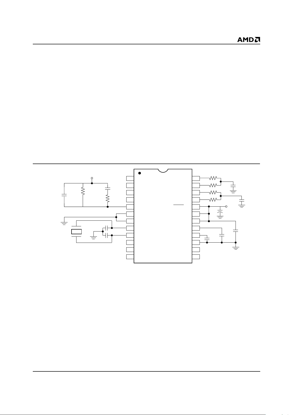
Differential l/O Terminations
The differential input for the Manchester data
(Receive±) is externally terminated by two 40.2-ohm
±1% resistors and one optional common-mode bypass
capacitor. The differential input impedance, Z
lDF
and
the common-mode input, Z
lCM
, are specified so that the
Ethernet specification for cable termination impedance
is met using standard 1% resistor terminators. The Collision± differential inputs are terminated in exactly the
same way as the receive inputs (see Figure 6).
Collision Detection
A transceiver detects collisions on the network and
generates a 10 MHz signal at the Collision± inputs. This
collision signal passes through an input stage that detects signal levels and pulse duration. When the signal
is detected by the Am7992B, it sets the CLSN line
HIGH. This condition continues for approximately
160ns after the last LOW-to-HlGH transition on
Collision±.
03378I-10
Notes:
1. Connect R1, R2, C1, C2 for 0 differential nontransmit. Connect to ground for logic 1 differential nontransmit.
2. Pin 20 shown for normal device operation.
3. The inclusion of C4 and C5 is necessary to reduce the common-mode loading on certain transceivers that are direct
coupled.
4. C2 reduces the amount of noise from the power supply and crosstalk from RCLK that can be coupled from TSEL through to
the transmit
±
outputs.
Figure 6. External Component Diagram
R
1
C
2
20 pF
R
2
C1680 pF
3 KΩ
100 pF
100 pF
20 MHz
Parallel Mode.
Crystal 50 pF
0.005% Accuracy
V
CC
4700 pF
0.1 µF
4.7 µF
V
CC
0.1 µF
C
5
C
4
0.1 µF
A
B
40.2 Ω 1%
40.2 Ω 1%
40.2 Ω 1%
40.2 Ω 1%
510 Ω
0.1 µF
1
2
3
4
5
6
7
8
9
10
11
12
24
23
22
21
20
19
18
17
16
15
14
13
CLSN
RX
RENA
RCLK
TSEL
GND1
GND2
X1
X2
TX
TCLK
TENA
Collision+
Collision–
Receive+
Receive–
TEST
V
CC1
V
CC2
PF
RF
GND3
Transmit+
Transmit–
Page 10

10 Am7992B
Jitter Tolerance Definition and Test
The Receive Timing—Start of Reception Clock Acquisition waveform diagram shows the internal timing relationships implemented for decoding Manchester data
in the Am7992B. The Am7992B utilizes a clock capture
circuit to align its internal data strobe with an incoming
bit stream. The clock acquisition circuitry requires four
valid bits with the values 1010. Clock is phase locked to
the negative transition at BCC of the second “0” in
thepattern.
Since data is strobed at 1/4 bit time, Manchester transitions that shift from their nominal placement through
1/4 bit time will result in improperly decoded data. For
IEEE 802.3/Ethernet, this results in the loss of a message. With this as the criterion for an error, a definition
of “jitter handling” is:
That peak deviation from nominal input transition
approaching or crossing 1/4 bit cell position for
which the Am7992B will properly decode data.
Four events of signal are needed to adequately test the
ability of the Am7992B to decode data properly from
the Manchester bit stream. For each of the four events,
two time points within a received message are tested
(See Input Jitter Timing Waveforms):
1.Jitter tolerance at clock acquisition, the measure of
clock capture (case 1–4).
2.Jitter tolerance within a message after the analogue
PLL has reduced clock acquisition error to a minimum (case 5–8).
The four events to test are shown in the Input Jitter
Timing Waveform diagram. They are:
1.BCC jitter for a 01-bit pattern
2.BCC jitter for a 10-bit pattern
3.BCB jitter for an 11-bit pattern
4.BCB jitter for an X0-bit pattern
The test signals utilized to jitter the input data are artificial in that they may not be realizable on networks (examples are cases 2, 3, and 4 at clock acquisition).
However, each pattern relates to setup and hold time
measurements for the data decode register (Figure 5).
Receive+ and Receive– are driven with the inputs
shown to produce the zero crossing distortion at the differential inputs for the applicable test. Cases 4 and 8
require only a single zero to implement when tested at
the end of message.
Levels used to test jitter are within the common-mode
and differential-mode ranges of the receive inputs and
also are available from automatic test equipment. It is
assumed that the incoming message is asynchronous
with the local TCLK frequency for the Am7992B. This
ensures that proper clock acquisition has been established with random phase and frequency error in incoming messages. An additional condition placed on
the jitter tolerance test is that it must meet all test requirements within 10 ms after power is applied. This
forces the Am7992B crystal oscillator to start and lock
the analog PLL to within acceptable limits for receiving
from a cold start.
Case 1 of the test corresponds to the expected
Manchester data at clock acquisition, and average values for clock leading jitter tolerance are 21.5 ns. For
cases 5 through 8, average values are 24.4 ns. Cases
5 through 8 are jittered at bit times 55 or 56 as applicable. The Am7992B, then, has on average 0.6 ns static
phase error for the noise-free case.
Page 11

AMD
11Am7992B
APPLICATION
RG58
BNC “T”
03378I-11
Local
CPU
Local
Memory
Am7990
LANCE
Am7992B
SIA
Power
Supply
Local Bus
ETHERNET
DTE
AUI – Attachment Unit Interface
DTE – Data Terminal Equipment
MAU – Medium Attachment Unit
Local
CPU
Local
Memory
Am7990
LANCE
Local Bus
CHEAPERNET
DTE
AUI
Cable
MAU
ETHERNET
COAX
TAP
Am7992B
SIA
Power
Supply
Am7996
Transceiver
Am7996
Transceiver
Figure 7. Typical ETHERNET Node
Page 12

AMD
12 Am7992B
ABSOLUTE MAXIMUM RATINGS
Storage Temperature –65°C to +150°C. . . . . . . . . . .
Ambient Temperature with
Power Applied 0°C to +70°C. . . . . . . . . . . . . . . . . . . .
Supply Voltage Continuous +7.0 V. . . . . . . . . . . . . . .
DC Voltage Applied to Outputs –0.5 V to V
CC
Max. . .
DC Input Voltage (Logic Inputs) +5.5 V. . . . . . . . . . .
DC Input Voltage
(Receive±/Collision±) –6 V to +16 V. . . . . . . . . . . . .
Transmit± Output Current –50 mA to +25 mA. . . . . .
DC Output Current, Into Outputs 100 mA. . . . . . . . . .
DC Input Current (Logic Inputs) ±30 mA. . . . . . . . . .
Transmit± Applied Voltage 0 V to +16 V. . . . . . . . . .
Stresses above those listed under Absolute Maximum Ratings may cause permanent device failure. Functionality at or
above these limits is not implied. Exposure to Absolute Maximum Ratings for extended periods may affect device reliability. Programming conditions may differ.
OPERATING RANGES
Commercial (C) Devices
Temperature (T
C
)0°C to +70°C. . . . . . . . . . . . . . . . .
Supply Voltage (V
CC
) +5.0 V ±10%. . . . . . . . . . . . . . .
Operating ranges define those limits between which the functionality of the device is guaranteed.
Page 13

AMD
13Am7992B
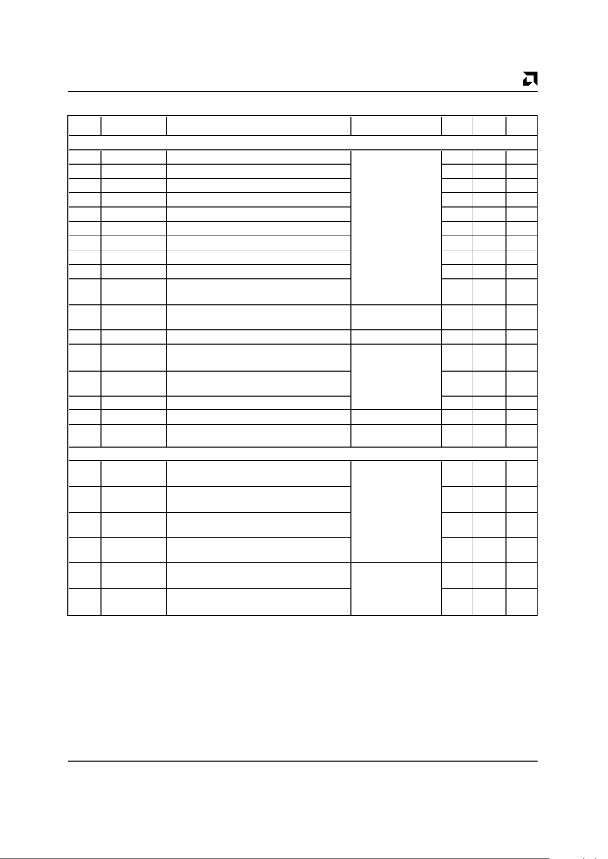
DC CHARACTERISTICS over operating ranges unless otherwise specified
Parameter
Symbol Parameter Description Test Conditions Min Max Unit
V
OH
Output HIGH Voltage RX, IOH = –1.0 mA, VCC = Min 2.4 V
RENA, CLSN, TCLK, RCLK
V
OL
Output LOW Voltage IOL = 16 mA, VCC = Min 0.5 V
RCLK, TSEL, TCLK, RENA, RX, CLSN I
OL
= 1 mA, VCC = Min 0.4 V
V
OD
Differential Output VoltageTX+ > TX– for VO RL = 78 Ω 550 770 mV
(Transmit+) – (Transmit–) TX+ < TX– for V
O
–550 –770 mV
V
OD OFF
Transmit Differential Output Idle Voltage VCC = Min, RL = 78 Ω (Note 1) –20 20 mV
I
OD OFF
Transmit Differential Output Idle Current TSEL = HIGH (Note 2) –0.5 0.5 mA
V
CMT
Transmit Output Common-Mode Voltage RL = 78 Ω, VCC = Min 0 5 V
V
ODI
Transmit Differential Output Voltage (Note 1) 20 mV
Imbalance
||V
O
| – |VO||
V
IH
Input HIGH Voltage TX, TENA 2.0 V
I
IH
Input HIGH Current TX, TENA, TEST VCC = Max, VIN = 2.7 V +50 µA
V
IL
Input LOW Current TX, TENA 0.8 V
I
IL
Input LOW Current TX, TENA, TEST VCC = Max, VIN = 0.4 V –400 µA
V
IRD
Differential Input Threshold (Receive Data) VCM = 0 V, (Note 4) Ceramic
Package –35 +35 mV
Plastic
Package –65 +65 mV
V
IRVD
Differential Mode Input Voltage Range (Note 3) –1.5 +1.5 V
(Receive ±/Collision ±)
V
IRVC
Receive ± and Collision ± Common (Note 2) 0 5.5 V
Mode Voltage
V
IDC
Differential Input Threshold to Detect Carrier VCM = 0 V (Note 4) –175 –275 mV
I
CC
Power Supply Current VCC = Max (Note 5) 180 mA
V
IB
Input Breakdown Voltage (TX, TENA, TEST)II = 1 mA, VCC = Max 5.5 V
V
IC
Input Clamp Voltage IIN = –18 mA, VCC = Min –1.2 V
V
ODP
Undershoot Voltage on Transmit (Note 3) –100 mV
Return to Zero (End of Message)
I
SC
Short Circuit Current VCC = Max (Note 6) –40 –150 mA
RCLK, RX, TCLK, CLSN, RENA
R
IDF
Differential Input Resistance VCC = 0 to Max (Note 3) 6 kΩ
R
ICM
Common Mode Input Resistance VCC = 0 to Max (Note 3) 1.5 kΩ
V
ICM
Receive and Collision Input Bias Voltage IIN = 0, VCC = Max 1.5 4.2 V
I
ILD
Receive and Collision Input LOW Current VIN = –1 V, VCC = Max –1.64 mA
I
IHD
Receive and Collision Input HIGH Current VIN = 6 V, VCC = Min +1.10 mA
I
IHZ
Receive and Collision Input HIGH VCC = 0, VIN = +6 V 1.86 mA
Current Power Off
I
IHX
Oscillator (X1) Input HIGH Current VIN = 2.4 V, VCC = Max +800 µA
I
ILX
Oscillator (X1) Input LOW Current VIN = 0.4 V, VCC = Max –1.2 mA
V
IHX
Oscillator (X1) Input HIGH Voltage (Note 3) 2.0 V
V
ILX
Oscillator (X1) Input LOW Voltage (Note 3) 0.8 V
Com’l
Note:
See notes following Switching Characteristics table.
Page 14
AMD
14 Am7992B
SWITCHING CHARACTERISTICS over operating ranges unless otherwise specified
(Note 8)
(Note 4)
(Note 4)
No. Parameters Description Test Conditions Min Max Unit
Receiver Specification
1t
RCT
RCLK Cycle Time 85 118 ns
2t
RCH
RCLK HIGH Time 38 ns
3t
RCL
RCLK LOW Time 38 ns
4t
RCR
RCLK Rise Time 8 ns
5t
RCF
RCLK Fall Time 8 ns
6t
RDR
RX Rise Time 8 ns
7t
RDF
RX Fall Time 8 ns
8t
RDH
RX Hold Time (RCLK ↑ to RX Change) 5 ns
9t
RDS
RX Prop Delay (RCLK ↑ to RX Stable) 25 ns
10 t
DPH
RENA Turn-On Delay (V
IDC
Max on 80 ns
Receive ± to RENA
H
)
11 t
DPO
RENA Turn-On Delay (V
IDC
Min on (Note 9) 300 ns
Receive ± to RENA
L
)
12 t
DPL
RENA LOW Time (Note 10) 120 ns
13 t
RPWR
Receive ± Input Pulse Width to Reject 20 ns
(|Input| > |V
IDC
Max|)
14 t
RPWO
Receive ± Input Pulse Width to Turn-On 45 ns
(|Input| > |V
IDC
Max|)
15 t
RLT
Decoder Acquisition Time 450 ns
16 t
REDH
RENA Hold Time (RCLK ↑ to RENAL)4080ns
17 t
RPWN
Receive ± Input Pulse Width to 165 ns
Not Turn-Off INTCARR
Collision Specification
18 t
CPWR
Collision ± Input Pulse Width to Not 10 ns
Turn-On CLSN (|Input| > |V
IDC
Min|)
19 t
CPWO
Collision ± Input Pulse Width to Turn-On 26 ns
CLSN (|Input| > |V
IDC
Max|)
20 t
CPWE
Collision ± Input Pulse Width to Turn-Off 160 ns
CLSN (|Input| > |V
IDC
Max|)
21 t
CPWN
Collision ± Input Pulse Width to Not 80 ns
Turn-Off CLSN (|Input| < |V
IDC
Max|)
22 t
CPH
CLSN Turn-On Delay (V
IDC
Max on 50 ns
Collision ± to CLSN
H
)
23 t
CPO
CLSN Turn-Off Delay (V
IDC
Max on 160 ns
Collision ± to CLSN
L
)
Page 15

AMD
15Am7992B
SWITCHING CHARACTERISTICS (continued)
*Min = 4.5 V, Max = 5.5 V, T
OSC
= 50 ns; in production test, all differential input test conditions are done single-ended,
non-V
IRD
levels are forces on DUT for waveform swing (levels chosen are due to tester limitations) and a distortion-free
preamble is applied to Receive
±
inputs.
Notes:
1. Tested but to values in excess of limits. Test accuracy not sufficient to allow screening guardbands.
2. Correlated to other tested parameter: I
OD
OFF = VOD OFF/R
L
.
3. Not tested.
4. Test done by monitoring output functionally.
5. Receive, Collision and Transmit functions are inactive: X1 driven by 20 MHz.
6. Not more than one output should be shorted at a time. Duration of the short circuit test should not exceed one second.
7. TCLK changes state on X1 rising edge, but initial state of TCLK is not defined. When TENA is High, TX data is
Manchester encoded on the falling edge of X1 after the rising edge of TCLK.
8. Assumes 50 pF capacitance loading on RCLK and RX.
9. Test is done only for last BIT = 1, which is worst case.
10.Test done from 0.8 V of falling to 2.0 V of rising edge.
11.Test correlated to T
TCH
.
12.Measured from 50% point of X1 driving the input in production test.
No. Parameters Description Test Conditions Min Max Unit
Transmitter Specification
24 t
TCL
TCLK LOW Time (Note 11) 45 ns
25 t
TCH
TCLK HIGH Time 45 ns
26 t
TCR
TCLK Rise Time 8 ns
27 t
TCF
TCLK Rise Time 8 ns
28 t
TDS
, t
TES
TX and TENA Setup Time to TCLK 5 ns
29 t
TDH
, t
TEH
TX and TENA Hold Time to TCLK 5 ns
30 t
TOCE
Transmit ± Output, (Bit Cell Center to Edge) 49.5 50.5 ns
31 t
OD
TCLK HIGH to Transmit ± Output 100 ns
32 t
TOR
Transmit ± Output Rise Time 4 ns
33 t
TOF
Transmit ± Output Fall Time 4 ns
34 t
XTCH X1
to TCLK Propagation Delay for HIGH 5 18 ns
35 t
XTCL X1
to TCLK Propagation Delay for LOW 5 18 ns
36 t
EJ1
Clock Acquisition Jitter Tolerance VCC = 5.0 V (Note 1) 16 21.5 ns
37 t
EJ51
Jitter Tolerance After 50 Bit Times VCC = 5.0 V (Note 1) 19 24.4 ns
(Note 1)
20% – 80%
(Notes 7 & 12)
Page 16

AMD
16 Am7992B
KEY TO SWITCHING WAVEFORMS
KS000010
Must be
Steady
May
Change
from H to L
May
Change
from L to H
Does Not
Apply
Don’t Care,
Any Change
Permitted
Will be
Steady
Will be
Changing
from H to L
Will be
Changing
from L to H
Changing,
State
Unknown
Center
Line is HighImpedance
“Off” State
WAVEFORM INPUTS OUTPUTS
Page 17

AMD
17Am7992B
SWITCHING WAVEFORMS
(Note A)(Note E)
Bit Cell 1
1
Bit Cell 2
0
Bit Cell 3
1
Bit Cell 4
0
Bit Cell 5
1
BCC1BCB BCC0BCB BCC1BCBBCC0BCB BCC1BCB
10
15
(Note D)
(Note B)
(Note C)
(Note F)
Receive±
(Measured
Differentially)
INTCARR
RENA
V
CO
Enable
V
CO
INTRCLK
RCK Enable
RCLK
RX
INTPLLCLK
03378I-12
Notes:
A. Minimum Width > 45 ns.
B. RCLK = INTRCLK when
TEST
LOW.
C. RX undefined until bit time 5 (1st decoded bit).
D. Oscillator Interrupt may occur at 2nd INTRCLK after Bit 2 Clock Transition.
E. Timing Diagram does not include Internal Propagation Delays.
F. First valid data at RX (Bit 5).
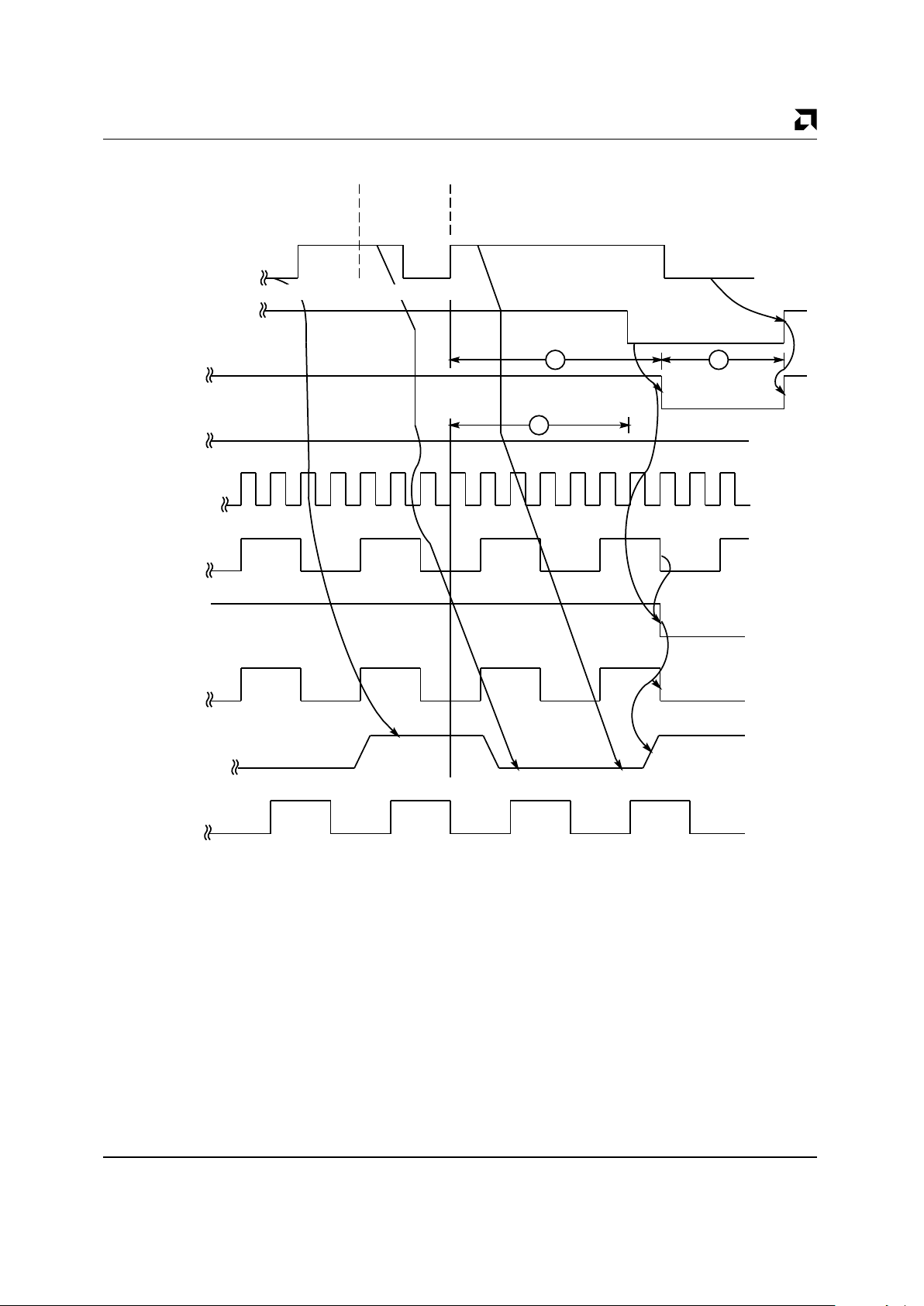
Receive Timing – Start of Reception Clock Acquisition
Page 18
AMD
18 Am7992B
SWITCHING WAVEFORMS
Bit (N – 1)
1
Bit N
0
BCC BCB BCC BCB
(Note A)
(Note B)
17
11 12
Bit (N – 1) Bit N
Receive+
(Measured
Differentially)
INTCARR
RENA
V
CO
Enable
V
CO
INTRCLK
RCK Enable
RCLK
RX
PLL CLK
03378I-13
Notes:
A. INTCARR deasserts 1.55 bit times after last Receive
±
Rising Edge.
B. Start of Next Packet.
Receive Timing – End of Reception (Last Bit = 0)
Page 19

AMD
19Am7992B
SWITCHING WAVEFORMS
11
16
Bit (N – 1) Bit N
(Note A)
17
Bit (N – 1)
Bit N
10
BCC BCB
Receive±
(Measured
Differentially)
INTCARR
V
CO
Enable
V
CO
INTRCLK
RCK Enable
RCLK
RX
PLL CLK
RENA
Note:
A. INTCARR deasserts 1.55 bit times after last Receive
±
Rising Edge.
03378I-14
BCC
Receive Timing – End of Reception (Last Bit = 1)
Page 20

AMD
20 Am7992B
SWITCHING WAVEFORMS
31
101
(Note A)
X1
TCLK
TENA
TSEL
Transmit+
Transmit–
Transmit±
(Measured
Differentially)
TX
03378I-15
V
H
V
H
V
L
V
L
(Note B)
(Note C)
(Note C)
(Note B)
Notes:
A. X1 20 MHz Sine Wave from Crystal Oscillator or driven with X1 driven from External Source Waveform.
B. TSEL connected as shown in Figure 2B. For Figure 2A, Transmit+ is HIGH when TENA is LOW.
C. When Idle Transmit
±
Zero Differential is 1/2 (VH + VL).
Transmit Timing – Start of Packet
Page 21

AMD
21Am7992B
SWITCHING WAVEFORMS
03378I-16
0.5 VO at 2 µs
0.5 VO at 2 µs
V
O
29
30
30
V
O
Bit (N – 2) Bit (N – 1) Bit N
BCC BCB BCC BCB BCC BCB
X1
TCLK
TENA
TSEL
CASE 1
TX (Last Bit = 0)
Transmit+
Transmit–
Transmit±
(Measured Differentially)
CASE 2
TX (Last Bit = 1)
Transmit+
Transmit–
V
O
V
O
Transmit±
(Measured Differentially)
Transmit Timing – End of Transmission*
*TSEL Components (see Figure 2B).
See Typical Performance Curve for Response at End of Transmission with Inductive Loads.
Page 22

AMD
22 Am7992B
SWITCHING WAVEFORMS
2322
2.0 V
.8 V
V
IDC
Max V
IDC
Max
+
0 V
–
Collision
Presence±
CLSN
03378I-17
Collision Timing
31
33 32
2 V2 V
80%
80%
50%
20% 20%
X1
TCLK
TENA
03378I-18
Transmit±
(Measured Differentially)
Transmit Timing (at start of packet)
Page 23

AMD
23Am7992B
SWITCHING WAVEFORMS
14
2.0 V
Receive±
(Measured Differentially)
03378I-19
17
13
10
0 V0 V
V
IRVD
+1.5 V
V
IRVD
–1.5 V
V
IDC
Min
(–175 mV)
V
IDC
Max
(–275 mV)
RENA
0 V
Receive± Input Pulse Width Timing
19
2.0 V
Collision±
(Measured Differentially)
03378I-20
20
18
22
0 V 0 V0 V
V
IRVD
+1.5 V
V
IRVD
–1.5 V
V
IDC
Min
(–175 mV)
V
IDC
Max
(–275 mV)
CLSN
21
Collision± Input Pulse Width Timing
0.8 V
0.2 V
9
8
5
1
3
2
4
8
0.8 V
2.0 V
RCLK
RX
03378I-21
6
7
RCLK and RX Timing
Page 24

AMD
24 Am7992B
SWITCHING WAVEFORMS
03378I-22
2.0 V
0.8 V
2.0
0.8
2.0
0.8
0.8 V 0.8 V
0.8 V
2.0 V
25 24
26 27
28 29
28
TCLK
TX
TENA
TCLK and TX Timing
T
OSC
0.8
2.0
1.5
1.51.5 1.5
X1
Driving
Input
TCLK
Transmit+, Transmit–
(Note A)
t
R
* tF*
t
HIGH
* t
LOW
*
0.8
2.0
35 34
‘A’ ‘B’
0 V
BCC
(Bit Cell Center)
BCB
(Bit Cell Boundary)
03378I-23
Note:
A. Encode Manchester clock transition (BCC) at Point ‘A’ and bit cell edge (BCB) at point ‘B’.
*See Specification for External TTL Level in Functional Description section.
X1 Driven from External Source
Page 25

AMD
25Am7992B
SWITCHING WAVEFORMS
12345 678
Bit Number
INTRCLK
PLL CLK
4.5 V
1.5 V
3 V
0
+4.5 V
1.5 V
0
–1.5 V
Receive+
Receive–
Receive±
RX
+3 V
0
+4.5 V
+1.5 V
0
–1.5 V
+1.5 V
–4.5 V
Receive+
Receive–
Receive±
RX
+3 V
0
+4.5 V
+1.5 V
0
–1.5 V
+1.5 V
Receive+
Receive–
Receive±
RX
+4.5 V
+1.5 V
+3 V
+1.5 V
0
–1.5 V
0
Receive+
Receive–
Receive±
RX
55 56 57 58
BCC BCC BCC BCC BCC BCC BCC BCC
BCB
1/4 Bit Cell
0 V
4.5 V
Strobe
RX
BCB
Strobe
RX
Strobe
RX
Strobe
RX
1/4 Bit Cell
BCB
03378I-24
(Note A)
(Note B)
(Note C)
(Note D)
Notes:
A. Case 1, 5 Data Bit Pattern 0, 1
Rising clock edge moved toward 1/4 bit cell RCLK data strobe. Case 1 uses bit 5, Case 5 uses bit 55.
B. Case 2, 6 Data Bit Pattern 1, 0
Falling clock edge moved toward 1/4 bit cell RCLK data strobe. Case 2 uses bit 6, Case 6 uses bit 56.
C. Case 3, 7 Data Bit Pattern 1, 1
Falling bit cell edge moved toward 1/4 bit cell RCLK data strobe. Case 3 uses bit 6, Case 7 uses bit 56.
D. Case 4, 8 Data Bit Pattern X, 0
Rising bit cell edge moved toward 1/4 bit cell RCLK data strobe. Case 4 uses bit 5, Case 8 uses bit 55.
tEJI
tEJ51
D
tEJI
tEJ51
C
tEJI
tEJ51
B
A
tEJI
tEJ51
Input Jitter Timing
Page 26

AMD
26 Am7992B
TYPICAL PERFORMANCE CURVE
600
500
400
300
200
100
0
–100
1.0 2.0 3.0 4.0 5.0 6.0
03378I-25
Time (µs)
Differential Output
Voltage (V
O
)
(mV)
End of Transmission – Differential Output Voltage*
Notes:
R = 78 Ω*
R = 78 Ω
L = 95 µH
3
R = 78 Ω
L = 75 µH
2
R = 78 Ω
L = 60 µH
1
LR
L Test
R Test
60 µH
Am7992B
75 µH NOM.
AUI
V
O
80.4
Am7996
75 µH NOM.
Am7992B
80.4
V
O
Am7996
95 µH
1. 802.3 Test Load:
2. 802.3 10BASE5 Network Connection:
3. 802.3 10BASE2 Network Connection:
*Equivalent Load:
03378I-26
Page 27

AMD
27Am7992B
SWITCHING TEST CIRCUITS
DUT
50 pF
DUT
Transmit–
R
L
= 78 Ω
Transmit+
03378I-27 03378I-28
DUT
–
+
03378I-29
DC Voltage
A. Test Load for RX, RENA, RCLK,
TCLK, CLSN
B. Transmit± Output
C. Receive± and Collision± Input
 Loading...