

Page 1

PRELIMINARY
Am55DL128C8G
Stacked Multi-Chip Package (MCP) Flash Memory and SRAM
T w o Am29DL640G 64 Megabit (4 M x 16-Bit) CMOS 3.0 Volt-only, Simultaneous Read/Write Flash
Memories and 64 Mbit (4 M x 16-Bit) Fast Cycle RAM
and 8 Mbit (512K x 16-Bit) Static RAM
DISTINCTIVE CHARACTERISTICS
MCP Features
■ Power supply voltage of 2.7 to 3.1 volt
■ High performance
— Access time as fast as 70 ns
■ Package
— 93-Ball FBGA
■ Op erating Temperature
— –40°C to +85°C
Flash Memory Features
ARCHITECTURAL ADVANTAGES
■ Simultaneous Read/Write operations
— Data can be continuously read from one bank while
executing erase/program functions in another bank.
— Zero latency between read and write operations
■ Flexible Bank architecture
— Read may occur in any of the three banks not being written
or erased.
— Four banks may be grouped by customer to achieve desi red
bank divisions.
■ Manufactured on 0.17 µm process technology
■ SecSi™ (Secured Silicon) Sector: Extra 256 Byte sector
— Factory locked and identifiable: 16 bytes available for
secure, random factory Electronic Serial Number; verifiable
as factory locked through autoselect function. ExpressFlash
option allows entire sector to be available for
factory-secured data
— Customer lockable: Sector is one-time pr ogrammable. Once
sector is locked, data cannot be changed.
■ Zero Power Operation
— Sophisticated power management circuits reduce power
consumed during inactive periods to nearly zero.
■ Boot sectors
— Top and bottom boot sectors in the same device
■ Compatible with JEDEC standards
— Pinout and software compatible with single-power-supply
flash standard
PERFORMANCE CHARACTERISTICS
■ High performance
— Access time as fast as 70 ns
— Program time: 4 µs/word typical utilizing Accelerate function
■ Ultra low power consumption (typical values)
— 2 mA active read current at 1 MHz
— 10 mA active read current at 5 MHz
— 200 nA in standby or automatic sleep mode
■ Minimum 1 million erase cycles guaranteed per sector
■ 20 year data retention at 125°C
— Reliable operation for the life of the system
SOFTWARE FEATURES
■ Data Management Software (DMS)
— AMD-supplied software manages data programming,
enabling EEPROM emulation
— Eases historical sector erase flash limitations
■ Supports Common Flash Memory Interface (CFI)
■ Program/Erase Suspend/Erase Resume
— Suspends program/erase operations to allow
programming/erasing in same bank
■ Data# Polling and Toggle Bits
— Provides a software method of detecting the status of
program or erase cycles
■ Unlock Bypass Program command
— Reduces overall programming time when issuing multiple
program command sequences
HARDWARE FEATURES
■ Any combination of sectors can be erased
■ Ready/Busy# output (RY/BY#)
— Hardware method for detecting program or erase cycle
completion
■ Hardware reset pin (RESET#)
— Hardware method of resetting the internal state machine to
the read mode
■ WP#/ACC input pin
— Write protect (WP#) function protects sectors 0 , 1, 140, and
141, regardless of sector protect status
— Acceleration (ACC) function accelerates program timing
■ Sec tor protection
— Hardware method of locking a sector, either in-system or
using programming equipment, to prevent any program or
erase operation within that sector
— Temporary Sector Unprotect allows changing data in
protected sectors in-system
FCRAM Features
■ Pow er dissipation
— Operating: 25 mA maximum
— Standby: 150 µA maximum
— Deep power-down standby: 10 µA
■ CE1s# and CE2s Chip Select
■ Power down features using CE1s# and CE2s
■ Data retention supply voltage: 2.7 to 3.1 volt
■ Byte data control: LB#s (DQ7–DQ0), UB#s (DQ15–DQ8)
SRAM Features
■ Pow er dissipation
— Operating: 30 mA maximum
— Standby: 15µA maximum
■ CE1s# and CE2s Chip Select
■ Power down features using CE1s# and CE2s
■ Data retention supply voltage: 1.5 to 3.1 volt
■ Byte data control: LB#s (DQ7–DQ0), UB#s (DQ15–DQ8)
This document contains information on a product under development at Advanced Micro Devices. The information
is intended to help you evaluate this product. AMD reserves the right to change or discontinue work on this proposed
product without notice.
Refer to AMD’s Website (www.amd.com) for the latest information.
Publication# 26829 Rev: A Amendment/0
Issue Date: October 25, 2002
Page 2
GENERAL DESCRIPTION
PRELIMINARY
Am29DL640G Features
The Am29DL640G is a 64 megabit, 3.0 volt-only flash
memory device, organized as 4,194,304 words of 16
bits each or 8,388,608 by tes of 8 bits each. Word
mode data appears on DQ15 –DQ0; byte mo de dat a
appears on D Q7–DQ0. The device is designed to be
programmed in-system with the stand ard 3.0 volt V
CC
supply, and can also be programmed in standard
EPROM programmers.
The device is available with an access time of 70 or 85
ns and is offered in a 93-ball FBGA package. Standard
control pins—chip enable (CE#f), write enable (WE#),
and output enable (OE#)—control n ormal read and
write operations, and avoid bus contention issues.
The device requires only a single 3.0 volt power sup-
ply for both read and write functions. Internally generated and regulated voltages are provi ded for the
program and erase operations.
Simultaneous Read/Write Operations with
Zero Latency
The Simultaneous Read/Write architecture provides
simultaneous operation by dividing the me mory
space into four banks , t wo 8 Mb banks with small and
large sectors, and two 24 M b banks of large s ectors
only. Sector addresses are fixed, system software can
be used to form user-defined bank groups.
During an Erase/Program operation, any of the three
non-busy banks may be read from. Note that only two
banks can operate simultaneously. The device can improve overall system performance by allowing a host
system to program or erase in one bank, then
immediately and si multaneously re ad from the othe r
bank, with zero latency. This releases the system from
waiting for the completion of program or erase
operations.
The Am29DL640 G can be organi zed as both a to p
and bottom boot sector configuration.
Bank Megabits Sector Sizes
Bank 1 8 Mb
Bank 2 24 Mb Forty-eight 64 Kbyte/32 Kword
Bank 3 24 Mb Forty-eight 64 Kbyte/32 Kword
Bank 4 8 Mb
The SecSi™ (Secured Silicon) Secto r is an extra
256 byte sec tor c apabl e of be ing pe rman ently lock ed
by AMD or customers. The SecSi Indicator Bit (DQ7)
is permanently set to a 1 if the part is factory locked,
and set to a 0 if customer lockable . This way, customer lockable parts can never be used to replace a
factory locked part.
Eight 8 Kbyte/4 Kword,
Fifteen 64 Kbyte/32 Kword
Eight 8 Kbyte/4 Kword,
Fifteen 64 Kbyte/32 Kword
Factory locked parts pro vide several options. Th e
SecSi Sector may store a secure, random 16 byte
ESN (Electronic Serial Numb er), cust omer code (programmed through AMD’s ExpressFlash service), or
both. Customer Lockable parts may utilize the SecSi
Sector as a one-time programmable area.
DMS (Data Management Software) allows systems
to easily take advantage of the advanced architecture
of the simultaneous read/write product line by allowing
removal of EEPROM devices. DMS will also allow the
system software to be simplified, as it will perform all
functions necessary to modify data in file structures,
as opposed to single-byte modifications. To write or
update a particular piece of data (a phone number or
configuration data, for example), the user only needs
to state which piece of data is to be updated, and
where the updated data is located in the system. This
is an advantage compared to systems where
user-written software must keep track of the old data
location, status, logical to physical translation o f the
data onto the Flash memory device (or memory devices), and more. Using DMS, user-written software
does not need to interface with the Flash memory directly. Instead, the user's software accesses the Flash
memory by calling one of only six functions. AMD provides this software to simplify system design and software integration efforts.
The device offers complete compatibility with the
JEDEC single-power-supply Flash command set
standard. Commands are written to the command
register using standard microprocessor write timings.
Reading data out of the device is similar to reading
from other Flash or EPROM devices.
The host system can detect whether a program or
erase operation is complete by using the device sta-
tus bits: RY/BY# pin, DQ7 (Data# Polling) and
DQ6/DQ2 (toggle bits). After a program or erase cycle
has been completed, the device automatically re turns
to the read mode.
The sector erase archite cture allow s memo ry sectors to be erased and reprogrammed without affecting
the data conten ts of oth er sec tors. Th e devi ce is fully
erased when shipped from the factory.
Hardware data protection measures include a low
detector that automatically inhibits write opera-
V
CC
tions during power transitions. The hardware sector
protection feature disables both program and erase
operations in any com bination of the secto rs of memory. This can be achieved in-system or via programming equipment.
The device offers two power-saving features. When
addresses have been stable for a specified amount of
time, the device enters the automatic sleep mode.
The system can also place the device into the
standby mode. Power consumption is greatly r educed in both modes.
2 Am55DL128C8G October 25, 2002
Page 3

PRELIMINARY
TABLE OF CONTENTS
Product Selector Guide . . . . . . . . . . . . . . . . . . . . . 5
MCP Block Diagram. . . . . . . . . . . . . . . . . . . . . . . . 5
Flash Memo r y Bl oc k Dia gram. . . . . . . . . . . . . . . . 6
Connection Diagram . . . . . . . . . . . . . . . . . . . . . . . . 7
Special Package Handling Instructions .................................... 7
Ordering Information . . . . . . . . . . . . . . . . . . . . . . . 9
MCP Device Bus Operations . . . . . . . . . . . . . . . .10
FCRAM Power Down Program . . . . . . . . . . . . . . .12
Table 2. Basic Key Table ................................................................12
Table 3. Available Key Table ..........................................................12
Flash Device Bus Operations . . . . . . . . . . . . . . .13
Requirements for Reading Array Data ...................................13
Writing Commands/Command Sequences ............................ 13
Accelerated Program Operation .......................................... 13
Autoselect Functions ........................................................... 13
Simultaneous Read/Write Operations with Zero Latency ....... 13
Automatic Sleep Mode ...........................................................14
RESET#: Hardware Reset Pin ............................................... 14
Output Disable Mode ..............................................................14
Table 4. Am29DL640G Sector Architecture ....................................15
Table 5. Bank Address ....................................................................18
Table 6. SecSi Sector Addresses ...............................................18
Table 7. Am29DL640G Boot Sector/Sector Block Addresses for Pro-
tection/Unprotection ........................................................................19
Write Protect (WP#) ................................................................ 19
Table 8. WP#/ACC Modes ..............................................................20
Temporary Sector Unprotect .................................................. 20
Figure 1. Temporary Sector Unprotect Operation........................... 20
Figure 2. In-System Sector Protect/Unprotect Algorithms .............. 21
SecSi™ (Secured Silicon) Sector
Flash Memory Region ............................................................ 22
Figure 3. SecSi Sector Protect Verify.............................................. 23
Hardware Data Protection ...................................................... 23
Low V
Write Pulse “Glitch” Protection ............................................23
Logical Inhibit ......................................................................23
Power-Up Write Inhibit ......................................................... 23
Common Flash Memory Interface (CFI) . . . . . . .23
Flash Command Definitions . . . . . . . . . . . . . . . . 27
Reading Array Data ................................................................ 27
Reset Command .....................................................................27
Autoselect Command Sequence ............................................27
Enter SecSi™ Sector/Exit SecSi Sector
Command Sequence .............................................................. 27
Word Program Command Sequence ..................................... 28
Unlock Bypass Command Sequence .................................. 28
Figure 4. Program Operation .......................................................... 29
Chip Erase Command Sequence ...........................................29
Sector Erase Command Sequence ........................................ 29
Erase Suspend/Erase Resume Commands ........................... 30
Figure 5. Erase Operation............................................................... 30
Flash Write Operation Status . . . . . . . . . . . . . . . . 32
Figure 6. Data# Polling Algorithm ................................................... 32
DQ7: Data# Polling .................................................................32
DQ6: Toggle Bit I .................................................................... 33
Figure 7. Toggle Bit Algorithm......................................................... 33
DQ2: Toggle Bit II ................................................................... 34
Write Inhibit ...........................................................23
CC
Reading Toggle Bits DQ6/DQ2 ............................................... 34
DQ5: Exceeded Timing Limits ................................................ 34
DQ3: Sector Erase Timer ....................................................... 34
Table 14. Write Operation Status ................................................... 35
Absolute Maximum Ratings . . . . . . . . . . . . . . . . 36
Figure 8. Maximum Negative Overshoot Waveform ...................... 36
Figure 9. Maximum Positive Overshoot Waveform........................ 36
Flash DC Characteristics . . . . . . . . . . . . . . . . . . 37
CMOS Compatible .................................................................. 37
Figure 10. I
Automatic Sleep Currents)............................................................. 40
Figure 11. Typical I
Current vs. Time (Showing Active and
CC1
vs. Frequency............................................ 40
CC1
MCP Test Conditions . . . . . . . . . . . . . . . . . . . . . . 41
Figure 12. Test Setup.................................................................... 41
Figure 13. Input Waveforms and Measurement Levels ................. 41
MCP AC Characteristics . . . . . . . . . . . . . . . . . . . 42
CE#s Timing ........................................................................... 42
Figure 14. Timing Diagram for Alternating Between
SRAM to Flash or FCRAM............................................................. 42
Flash AC Characteristics . . . . . . . . . . . . . . . . . . 43
Flash Read-Only Operations ................................................. 43
Figure 15. Read Operation Timings ............................................... 43
Hardware Reset (RESET#) .................................................... 44
Figure 16. Reset Timings............................................................... 44
Erase and Program Operations ..............................................45
Figure 17. Program Operation Timings.......................................... 46
Figure 18. Accelerated Program Timing Diagram.......................... 46
Figure 19. Chip/Sector Erase Operation Timings .......................... 47
Figure 20. Back-to-back Read/Write Cycle Timings ...................... 48
Figure 21. Data# Polling Timings (During Embedded Algorithms) . 48
Figure 22. Toggle Bit Timings (During Embedded Algorithms) ...... 49
Figure 23. DQ2 vs. DQ6................................................................. 49
Temporary Sector Unprotect .................................................. 50
Figure 24. Temporary Sector Unprotect Timing Diagram .............. 50
Figure 25. Sector/Sector Block Protect and
Unprotect Timing Diagram ............................................................. 51
Alternate CE#f Controlled Erase and Program Operations .... 52
Figure 26. Flash Alternate CE#f Controlled Write (Erase/Program)
Operation Timings.......................................................................... 53
Read Cycle .............................................................................54
Figure 27. SRAM Read Cycle—Address Controlled...................... 54
Figure 28. SRAM Read Cycle........................................................ 55
Write Cycle ............................................................................. 56
Figure 29. SRAM Write Cycle—WE# Control................................ 56
Figure 30. SRAM Write Cycle—CE#1s Control ............................. 57
Figure 31. SRAM Write Cycle—UB#s and LB#s Control ............... 58
FCRAM AC CHaracteristics . . . . . . . . . . . . . . . . 59
Read Operation ......................................................................59
Write Operation ....................................................................... 60
Power Down and Power Down Program Parameters ............. 61
Other Timing Parameters ....................................................... 61
AC Test Conditions .................................................................62
Read Timing ...........................................................................62
Figure 32. OE# Control Access...................................................... 62
FCRAM AC Characteristics .................................................... 63
Figure 33. CE#1 Control Access.................................................... 63
Figure 34. Address after OE# Control Access ............................... 63
Figure 35. Address Access after CE#1 Control Access................. 64
Figure 36. CE#1 Control ................................................................ 64
October 25, 2002 Am55DL128C8G 3
Page 4

PRELIMINARY
Figure 37. WE# Control Single Write Operation ............................. 65
Figure 38. WE# Control Continuous Write Operation ..................... 65
Figure 39. Read/Write Timing CE#1 Control,
Read Cycle First.............................................................................. 66
Figure 40. Read/Write Timing CE#1 Control,
Write Cycle First.............................................................................. 66
Figure 41. Read (OE# Control)/Write (WE# Control) Timing,
Read Cycle First.............................................................................. 67
Figure 42. Read (OE# Control)/Write (WE# Control) Timing,
Write Cycle First.............................................................................. 67
Figure 43. Power Down Program Timing........................................ 68
Figure 44. Power Down Program Timing........................................ 68
Figure 45. Power Down Entry and Exit Timing ............................... 68
Figure 46. Power Up Timing #1 ...................................................... 69
Figure 47. Power Up Timing #2 ...................................................... 69
Figure 48. Standby Entry Timing after Read or Write ..................... 69
FCRAM Data Retention . . . . . . . . . . . . . . . . . . . . 70
Low VDD Characteristics ........................................................ 70
Figure 49. Data Retention Timing.................................................. 70
Flash Erase And Programming Performance . . 71
Latchup Characteristics. . . . . . . . . . . . . . . . . . . . 71
BGA Package Pin Capacitance . . . . . . . . . . . . . . 71
Data Retention. . . . . . . . . . . . . . . . . . . . . . . . . . . . 71
SRAM Data Retention . . . . . . . . . . . . . . . . . . . . . 72
Figure 50. CE#1s Controlled Data Retention Mode....................... 72
Figure 51. CE2s Controlled Data Retention Mode......................... 72
Physical Dimensions . . . . . . . . . . . . . . . . . . . . . . 73
FNA093—93-Ball Fine-Pitch Grid Array 10 x 10 mm ............. 73
Revision Summary . . . . . . . . . . . . . . . . . . . . . . . . 74
4 Am55DL128C8G October 25, 2002
Page 5
PRELIMINARY
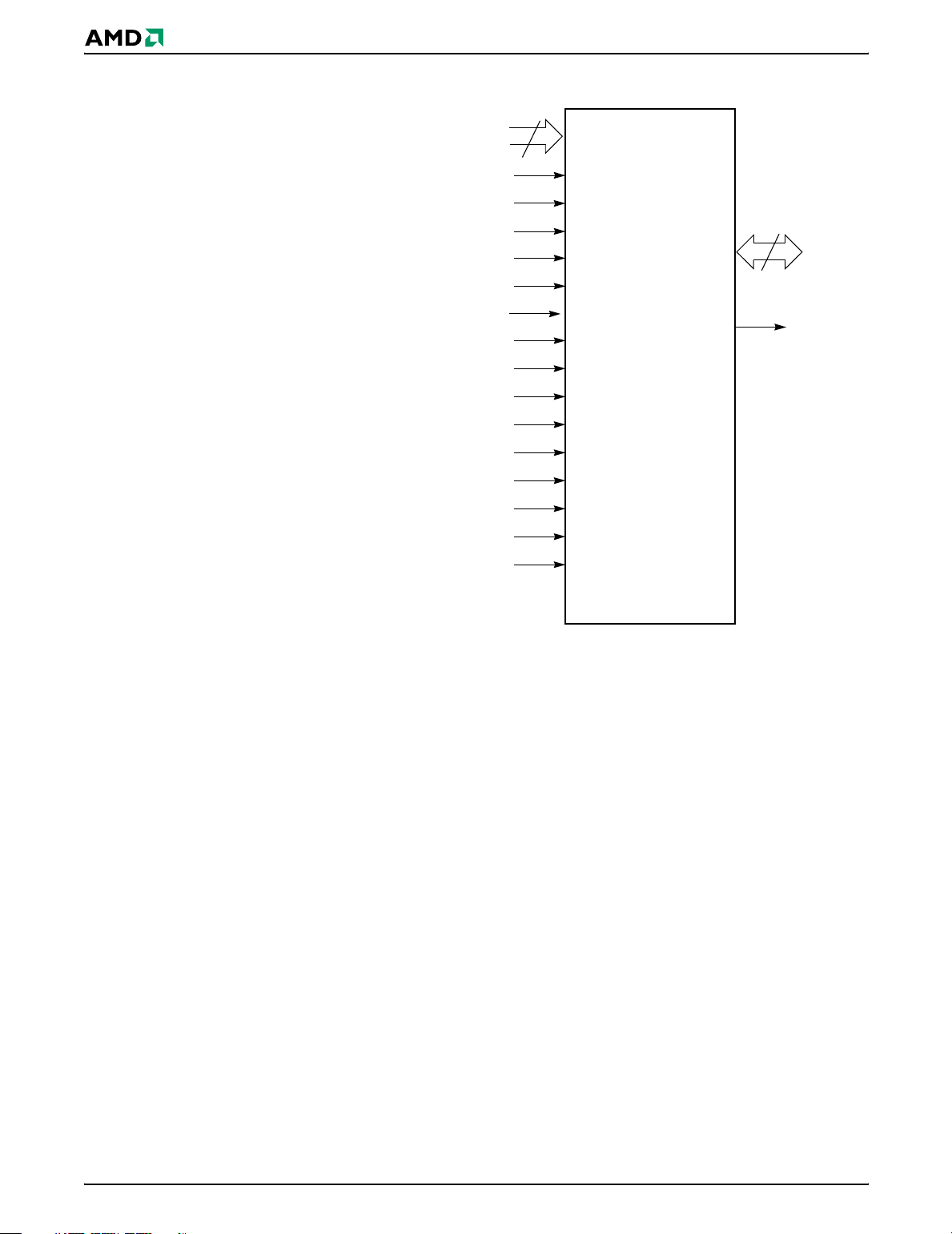
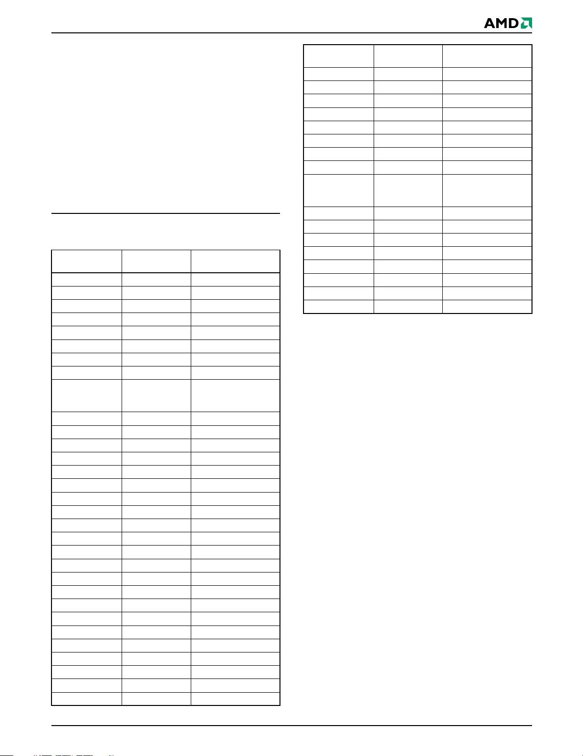
PRODUCT SELECTOR GUIDE
Part Number Am55DL128C8G
Speed
Options
Standard Voltage Range:
V
= 2.7–3.1 V
CC
Flash Memory Pseudo SRAM
70 85 70 85
Max Access Time, ns 70 85 70 85
CE#f Access, ns 70 85 70 85
OE# Access, ns 30 40 40 40
MCP BLOCK DIAGRAM
#1
V
SS
RY/BY#1
DQ15 to DQ0
V
SS
VCCf
A21 to A0
CE#f1
RESET #1
64 MBit
Flash Memory
VCCf
WP#/ACC
RESET#2
CE#f2
PE#
LB#s
UB#s
WE#
OE#
CE1#fc
CE2fc
CE1#s
CE2s
A21 to A0
A21 to A0
A18 to A0
Flash Memory
VCCs/V
CCQ
Fast Cycle
64 MBit
#2
64 MBit
RAM
8 MBit
SRAM
VSS/V
RY/BY#2
DQ15 to DQ0
DQ15 to DQ0
SSQ
DQ15 to DQ0
DQ15 to DQ0
October 25, 2002 Am55DL128C8G 5
Page 6
PRELIMINARY
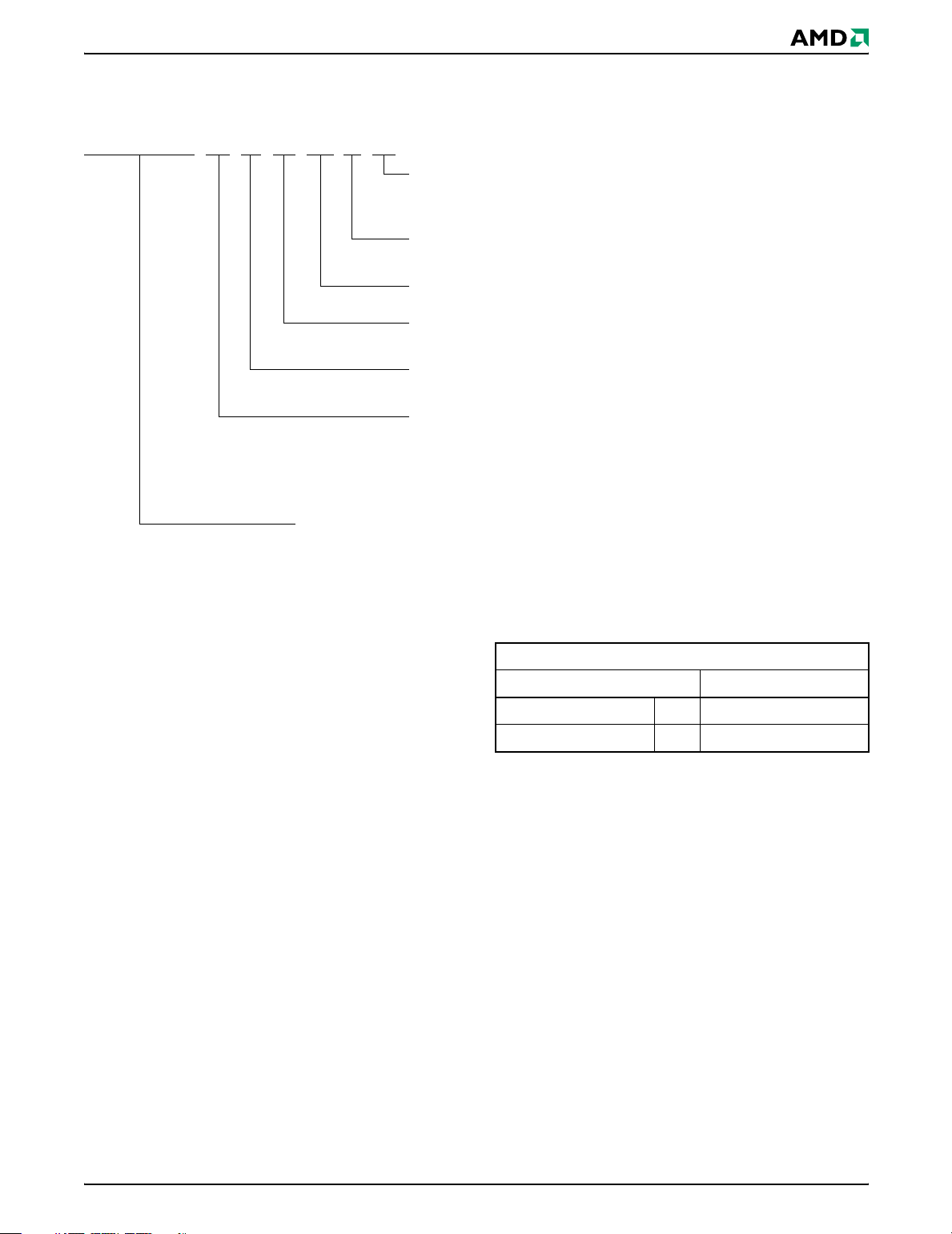
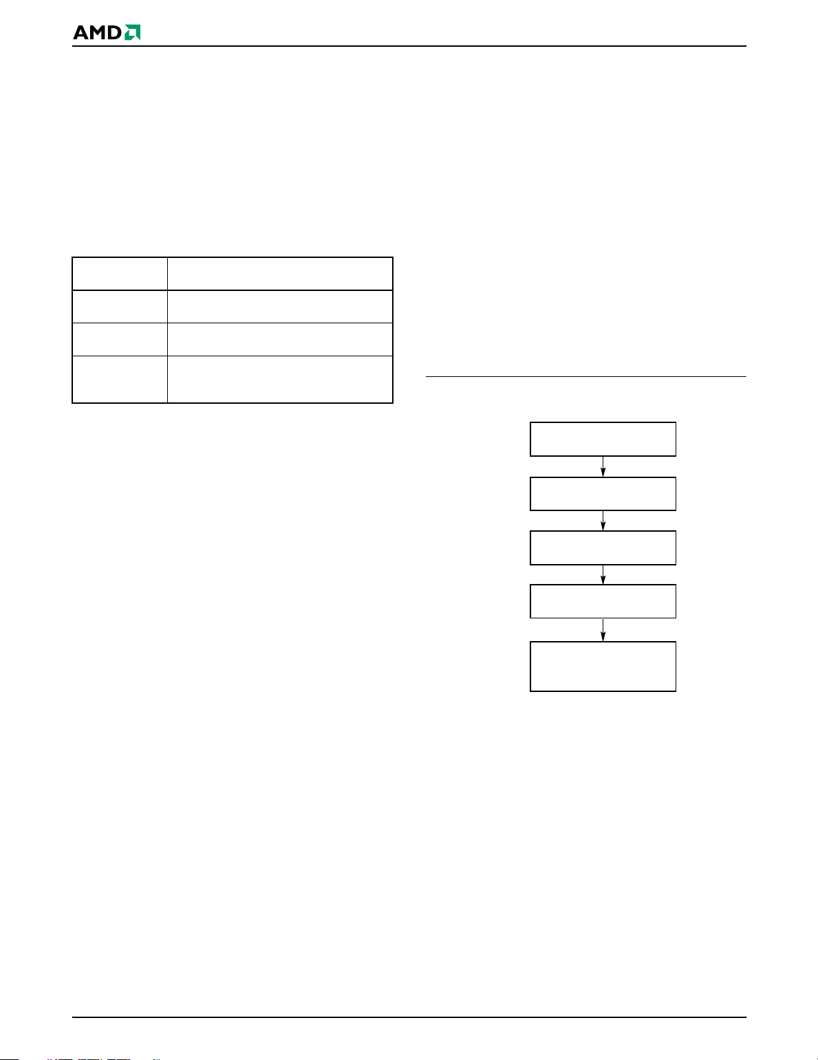
FLASH MEMORY BLOCK DIAGRAM
V
CC
V
SS
OE# BYTE#
A21–A0
A21–A0
RESET#
WE#
CE#
BYTE#
WP#/ACC
DQ15–DQ0
A21–A0
Mux
RY/BY#
A21–A0A0–A21
STATE
CONTROL
&
COMMAND
REGISTER
Mux
Bank 1 Address
Bank 2 Address
Bank 3 Address
Bank 4 Address
Status
Control
Bank 1
X-Decoder
Bank 2
X-Decoder
X-Decoder
Bank 3
X-Decoder
Bank 4
Y-gate
Y-gate
DQ15–DQ0
DQ15–DQ0
DQ15–DQ0
Mux
DQ15–DQ0
DQ15–DQ0
6 Am55DL128C8G October 25, 2002
Page 7
CONNECTION DIAGRAM
PRELIMINARY
93-Ball FBGA
Top View
Flash 1 only
A1
NC
B1
NC
C1
NC
F1
NC
G1
NC
B2 B3 B7 B8
NC VSSRY/BY#2
C2 C9
NC NC
D2
A3
E2
A2
F2
A1
G2
A0
H2
CE#f1
J2
CE1#FC
K2
NC NC
C3
A7
D3
A6
E3
A5
F3
A4
G3
V
H3
OE#
J3
DQ0
K3
DQ8
B4 B9
C4
LB#s
D4
UB#s
E4
A18
F4
A17
G4
DQ1
SS
H4
DQ9
J4
DQ10
K4
DQ2
B5
CE#f2
C5
WP#/ACC
D5
RESET#1
E5
RY/BY#1
F5
CE#1s NC
G5
V
CC
H5
DQ3
J5
V
K5
DQ11
CC
s
f
B6
NC
C6
WE#
D6
CE2FC
E6
A20
F6
G6
CE2s
H6
DQ4
J6
V
FC
CC
K6
NC
NC NC
C7
A8
D7
A19
E7
A9
F7
A10
G7
PE#FC
DQ6
H7
DQ13
J7
DQ12
K7
DQ5
C8
A11
D8
A12
E8
A13
F8
A14
G8
H8
DQ15
J8
DQ7
K8
DQ14
NC
D9
A15
E9
A21
F9
NC
G9
A16
H9
V
J9
V
K9
CC
SS
A10
NC
B10
NC
F10
NC
Flash 2 only
FCRAM only
Flash 1 and 2
shared
Shared
FCRAM & SRAM
Shared
2nd SRAM only
G10
NC
f
L1
NC
L2 L3 L4 L5 L6 L7 L8 L9
NC RESET#2 V
SS
VCCf
NC
M1
NC
Special Package Handling Instructions
Special handling is required fo r Flash Memo ry products in m olde d pa ckage s (B GA). The package and/or
NC NC NC
data integrity may be compromised if the package body
is exposed to temperatures above 150°C for prolonged
periods of time.
L10
NC
M10
NC
October 25, 2002 Am55DL128C8G 7
Page 8
PRELIMINARY
PIN DESCRIPTION
A18–A0 = 19 Address Inputs (Common)
A21–A19 = 2 Address Inputs (Flash + FCRAM)
DQ15–DQ0 = 16 Data Inputs/Outputs (Common)
CE#f1 = Chip Enable 1 (Flash)
CE#f2 = Chip Enable 2 (Flash)
OE# = Output Enable (Common)
WE# = Write Enable (Common)
RY/BY#1 = Ready/Busy Output 1 (Flash 1)
RY/BY#2 = Ready/Busy Output 2 (Flash 2)
UB#s = Upper Byte Control (FCRAM +
SRAM)
LB#s = Lower Byte Control (FCRAM +
SRAM)
RESET#1 = Hardware Reset Pin, Active Low
(Flash 1)
RESET#2 = Hardware Reset Pin, Active Low
(Flash 2)
WP#/ACC = Hardware Write Protect/
Acceleration Pin (Flash)
LOGIC SYMBOL
19
A18–A0
A21–A19
CE#f1
CE#f2
CE#1FC
CE2FC
PE#FC
CE#1s
CE2s
OE#
WE#
WP#/ACC
RESET#1
RESET#2
UB#s
LB#s
16 or 8
DQ15–DQ0
RY/BY#
f = Flash 3.0 volt-only single power sup-
V
CC
ply (see Product Selector Guide for
speed options and voltage supply
tolerances)
s = SRAM Power Supply
V
CC
V
SS
= Device Ground (Common)
NC = Pin Not Connected Internally
CE#1FC = Chip Enabled #1 (FCRAM)
CE2FC = Chip Enable #2 (FCRAM)
CE#1s = Chip Enable #1 (SRAM)
CE2s = Chip Enable #2 (SRAM)
FC = FCRAM power supply
V
CC
PE#FC = FCRAM power down enable
8 Am55DL128C8G October 25, 2002
Page 9
PRELIMINARY
ORDERING INFORMATION
The order number (Valid Combination) is formed by the following:
Am55DL128 C 8 G 70 L T
TAPE AND REEL
T=7 inches
S = 13 inches
TEMPERATURE RANGE
L = Light Industrial (–30
SPEED OPTION
See “Product Selector Guide” on page 5
PROCESS TECHNOLOGY
G = 0.17 µm
SRAM Device Density
8 = 8 Mbits
FAST CYCLE RAM DEVICE DENSITY
C= 64 Mbits
°C to +85°C)
AMD DEVICE NUMBER/DESCRIPTION
Am55DL128C8G
Stacked Multi-Chip Package (MCP) Flash Memory and SRAM
Two Am29DL640G 64 Megabit (4 M x 16-Bit) CMOS 3.0 Volt-only, Simultaneous Operation
Flash Memories and 64 Mbit (4 M x 16-Bit) FastCycle RAM and 8 Mbit (512K x 16 bit) SRAM
Valid Combinations
Valid Comb inations list configurations planned to be supported in volume for this device . Consult the lo cal AMD sales office t o confirm
availability of specific valid combinations and to check on newly released combinations.
Valid Combinations
Order Number Package Marking
Am55DL128C8G70L T, S M550000000
Am55DL128C8G85L T, S M550000001
October 25, 2002 Am55DL128C8G 9
Page 10

PRELIMINARY
MCP DEVICE BUS OPERATIONS
This section describes the requirements and use of
the device bus operations, which are in itiated through
the internal command register. The command register
itself does not occupy any addressabl e memory l ocation. The register is a latch used to store the commands, along with the ad dress and da ta information
needed to execute the command. The contents of the
register serve as inputs to the intern al state machine.
The state machine outputs dictate the function of the
device. Tables 1-2 lists the device bus operations, the
inputs and control levels they require, and the resulting output. The following subsections describe each of
these operations in further detail.
10 Am55DL128C8G October 25, 2002
Page 11
PRELIMINARY
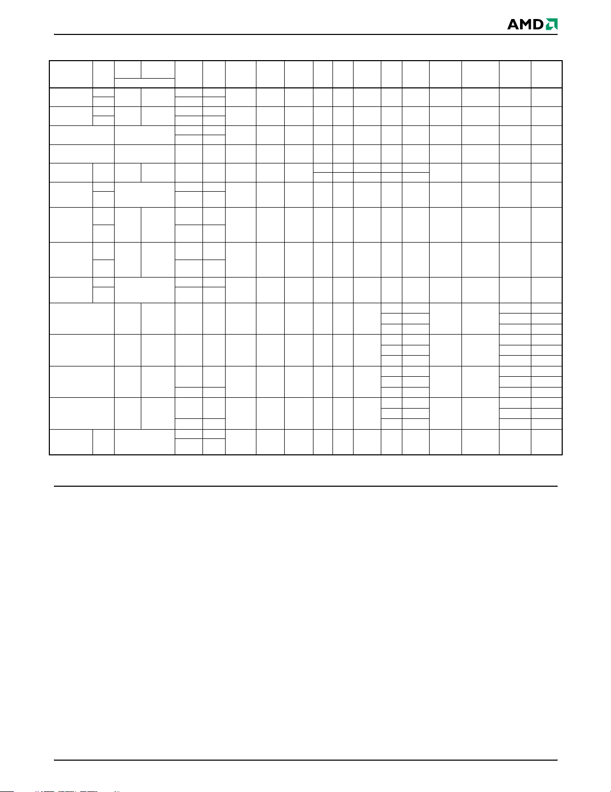
Table 1. Device Bus Operations—Flash Word Mode, (Notes 1, 2, 3)
CE#f
Operation
Active
Notes
Read from
Active Flash
Write to
Active Flash
9
10 X L
9
10 X L
Standby
Deep Power-down
Standby
Output
Disable
Flash
Hardware
Reset
Sector
Protect
Sector
Unprotect
Temporary
Sector
Unprotect
11
9
10 X L
7, 9,
11
7, 10,
11
7, 9,
11
7, 10,
11
9
10 X L
Read from SRAM H H L H H H H L H
Write to SRAM H H L H H H H X L
Read from FCRAM
Write to FCRAM
Power Down
Program
13
CE#f
Inactive
CE#1s CE2s CE#1FC CE2FC PE#FC OE# WE# Addr. LB#s UB#s RESET#
(Note 3)
LH
LH
± 0.3 V
V
CC
± 0.3 V
V
CC
HX
HX
HH
XL
HHHLH
HHHHL
H H HXXXXX
NA NA X L X X X X X X
LHLHLHH
X
HX
H H H X X X X X L L/H High-Z High-Z
HX
LH
HHHHL
XL
HX
LH
HHHHL
XL
X
HH
HX
HX
H H HXXXXX
LHHLHA
XL LH
HH
HX
LHHHLA
XL LH
V
± 0.3 V
CC
HX
XL
HHLXX
HH X X X
HH X X X
A
IN
A
IN
SADD,
A6 = L,
A1 = H,
A0 = L
SADD,
A6 = H,
A1 = H,
A0 = L
A
IN
A
IN
IN
IN
Key
(12)
WP#/ACC
(Note 6)
XX H L/H
XX H 6
±
V
CC
0.3 V
V
±
CC
0.3 V
DQ7–
DQ15–
DQ0
D
OUT
D
IN
H High-Z High-Z
H High-Z High-Z
H L/H High-Z High-Z
XX
XX
V
V
V
L/H
ID
ID
ID
8
8
LL
HL High-Z
HX
LH
LL
HL High-Z
HX
LH
LL
HL High-Z
HX
LL
HL High-Z
XX
HX
±
V
CC
0.3 V
H High-Z High-Z
D
IN
D
IN
D
High-Z
IN
D
OUT
D
High-Z
OUT
D
IN
D
High-Z
IN
D
OUT
D
High-Z
OUT
D
OUT
D
High-Z
OUT
DQ8
D
OUT
D
X
X
D
OUT
D
OUT
D
D
D
OUT
D
OUT
D
OUT
D
OUT
IN
IN
IN
Legend: L = Logic Low = VIL, H = Logic High = VIH, VID = 11.5–12.5 V, VHH = 9.0 ± 0.5 V, X = Don’t Care, SADD = Flash Sector Address, AIN =
Address In, D
= Data In, D
IN
= Data Out
OUT
Notes:
1. Other operations except for those indicated in this column are
inhibited.
2. Do not apply CE#f1 or 2 = VIL, CE#1s = VIL and CE2s = VIH at the
same time.
3. All operations assume FCRAM is in standby. To put in Power
Down program PE must be Low. To put in Power Down CE2 must
be Low.
4. Active flash is device being addressed.
5. Don’t care or open LB#s or UB#s.
6. If WP#/ACC = V
= V
the boot sectors protection will be removed.
IH
If WP#/ACC = V
40%.
, the boot sectors will be protected. If WP#/ACC
IL
(9V), the program time will be reduced by
ACC
8. If WP#/ACC = V
protected. If WP#/ACC = V
protection depends on whether they were last protected or
unprotected using the method described in “Sector/Sector Block
Protection and Unprotection”. If WP#/ACC = V
be unprotected.
9. Data will be retained in FCRAM.
10. Data will be lost in FCRAM.
11. CE# inputs on both flash devices may be held low for this
operation.
12. See “Power Down Program Key Table” on p. 13
13. Valid for FCRAM only.
, the two outermost boot sectors remain
IL
, the two outermost boot sector
IH
all sectors will
HH,
7. The sector protect and sector unprotect functions may also be
implemented via programming equipment. See the “Sector/Sector
Block Protection and Unprotection” section.
October 25, 2002 Am55DL128C8G 11
Page 12
PRELIMINARY
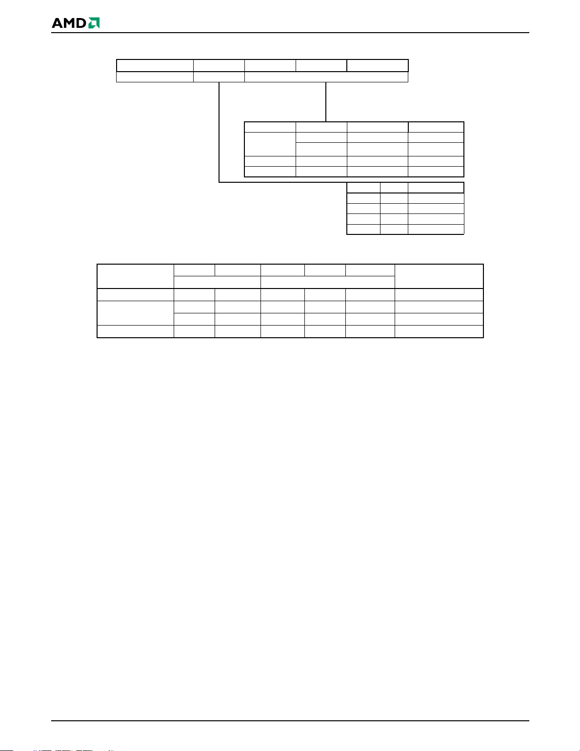
FCRAM POWER DOWN PROGRAM
Definition A0 A8 A21 A20
KEY Mode Select Area Select
Table 2. Basic Key Table
Mode
NAP L L X X X None
16M Partial
SLEEP H H X X X None
A0 A8 A18 A21 A20
Mode Select Area Select
H L L L L Bottom 16M only
H L H H H Top 16M only
A18 A21 A20 AREA
L
L
LLBOTTOM (2)
HXRESERVED
H L X RESERVED
H H H TOP (3)
A0 A8 Mode
LLNAP (4)
LHRESERVED
HL16M Partial
H H SLEEP (4, 5)
Data Retention Area
Table 3. Available Key Tabl e
Notes:
1. The Power Down Program can be perfor med one t i me aft er co mpl i anc e of P ower-up timings and it should not be re-programm ed af ter re gul ar Read
or Write. Unspecified addresses, A1 to A7, A9 to A17 and A19, can be either High or Low during the programming. The RESERVED key should not
be used.
2. BOTTOM area is from the lowest address location.
3. TOP area is from the highest address location.
4. NAP and SLEEP do not retain the data and Area Select is ignored.
5. Default state. Power Down Program to this SLEEP mode can be omitted.
12 Am55DL128C8G October 25, 2002
Page 13

PRELIMINARY
FLASH DEVICE BUS OPERATIONS
Requirements for Reading Array Data
To read array data from the outputs, the system must
drive the CE#f and OE# pins to V
. CE#f is the power
IL
control and selects the device. OE# is the output control and gates array data to the output pins. WE#
should remain at V
.
IH
The internal state machine is set for reading array data
upon device power-up, or after a hardware reset. This
ensures that no spurious alteration of the memory
content occurs durin g the power transition. No command is necessary in this mode to obtain array data.
Standard microprocessor read cycles that assert valid
addresses on the device address inputs produce valid
data on the device data outputs. Each bank remains
enabled for read access until the command register
contents are altered.
Refer to the Flash Read-Only Operations table for timing specifications and to Figure 15 for the timing diagram. I
in the DC Characteristics table represents
CC1
the active current specification for reading array data.
Writing Commands/Command Sequences
To write a command or command sequence (which includes programming data to the device and erasing
sectors of memory), the system must drive WE# and
CE#f to V
For program operations, the CIOf pin determines
whether the device accepts program data in bytes or
words. Refer to “Flash Device Bus Operations” for
more information.
The device features an Unlock Bypass mode to facilitate faster programming. Once a bank enters the Unlock Bypass mode, only two write cycles are required
to program a word or byte, instead of four. The “Word
Program Command Sequence” section has details on
programming data to the device using both standard
and Unlock Bypass command sequences.
An erase operation can erase one sector, multiple sectors, or the entire device. Table 4 indicates the address
space that each sector occupies. Similarly, a “sector
address” is the address bits required to uniquel y select
a sector. The “Flash Command Definitions” section
has details on erasing a sector or the entire chip, or
suspending/resuming the erase operation.
The device address space is divided into four banks. A
“bank address” is the address bits required to uniquely
select a bank.
, and OE# to VIH.
IL
Accelerated Program Operation
The device offers accelerated program operations
through the ACC function. This is one of two functions
provided by the WP#/ACC pin. This function is primarily intended to allow faster manu facturing throu ghput
at the factory.
If the system asserts V
on this pin, the device auto-
HH
matically enters the aforementioned Unlock Bypass
mode, temporarily unprotects any protec ted sectors,
and uses the higher voltage on the pin to reduce the
time required for program operations. The system
would use a two-cycle progra m command sequence
as required by the Unlock Bypass mode. Removing
from the WP#/ACC p in returns th e device to nor-
V
HH
mal operation. Note that V
must not be asserted on
HH
WP#/ACC for operations other than accelerated programming, or device damage may result. In addition,
the WP#/ACC pin must not be left floa ting or unconnected; inconsistent behavior of the device may result.
See “Write Protect (WP#)” on page 19 for related information.
Autoselect Functions
If the system writes the autoselect command s equence, the device enters the autoselect mo de. The
system can then read autoselect codes from the internal register (which is separate from the memory array)
on DQ15–DQ0. Standard read cycle timings apply in
this mode. Refer to the Sector/Sector Block Protection
and Unprotection and Autoselect Command Sequence sections for more information.
Simultaneous Read/Write Operations with Zero Latency
This device is c apable of r eading da ta from on e bank
of memory while programming or erasing in the other
bank of memory. An erase operation may also be suspended to read from or program to another location
within the same bank (except the sector being
erased). Figure 20 shows how read and write cycles
may be initiated for simultaneous operation with zero
latency. I
CC6
f and I
f in the table represent the cur-
CC7
rent specifications for read- while-program and
read-while-erase, respectively.
Standby Mode
When the system is n ot reading or wri ting to the device, it can place the device in the standby mode. In
this mode, current consum ption is greatly reduc ed,
and the outputs are placed in the high impedance
state, independent of the OE# input.
in the DC Characteristics table represents the ac-
I
CC2
tive current specification for the write mode. The Flash
AC Characteristics section contains timing specification tables and timing diagrams for write operations.
The device enters the CMOS standby mode when the
CE#f and R ESET # pins are bo th hel d at V
± 0.3 V.
CC
(Note that this is a more restricted voltage range tha n
.) If CE#f and RESET# are h eld at VIH, but not
V
IH
October 25, 2002 Am55DL128C8G 13
Page 14

PRELIMINARY
within V
± 0.3 V, the device will be in the standby
CC
mode, but the standby current will be greater. The device requires standard access time (t
) for read ac-
CE
cess when the device is in either of these standby
modes, before it is ready to read data.
If the device is deselected during erasure or programming, the device draws active current until the
operation is completed.
f in the table represents the standby current spec-
I
CC3
ification.
Automatic Sleep Mode
The automatic sleep mode minimizes Flash device energy consumption. The device automatically enables
this mode when addresses remain stable for t
ACC
+
30 ns. The automatic sleep mode is independent of
the CE#f, WE#, and OE# control signals. Standard address access timings provide new data when addresses are changed. While in sleep mode, output
data is latched and always available to the system.
f in the table represents the automatic sleep mode
I
CC5
current specification.
RESET#: Hardware Reset Pin
The RESET# pin provides a hardware me thod of resetting the device to reading array data. When the RESET# pin is driven low for at least a period of t
device immediately term inates any operation in
progress, tristates all output pins, and ignores all
read/write command s for the duration o f the RESE T#
pulse. The device also resets the internal state machine to reading array data. The operation that was interrupted should be reinitiated once the device is
RP
, the
ready to accept another command sequence, to ensure data integrity.
Current is reduced for the duration of the RESET#
pulse. When RESET# is held at V
draws CMOS standby current (I
held at V
but not within VSS±0.3 V, the standby cur-
IL
±0.3 V, the device
SS
f). If RESET# is
CC4
rent will be greater.
The RESET# pin may be tied to the system reset cir-
cuitry. A system reset would thus also reset the Flash
memory, enabling the system to read the boot-up firmware from the Flash memory.
If RESET# is a sserted during a prog ram or erase operation, the RY/BY# pin remains a “0” (busy) until the
internal reset operation is complete, which requires a
time of t
(during Embedded Algorithms). The
READY
system can thus monitor RY/BY# to determine
whether the reset operation is complete. If RESET# is
asserted when a program or erase operation is not executing (RY/BY# pin is “1”), the reset operation is completed within a time of t
Algorithms). The system can read data t
RESET# pin returns to V
(not during Embedded
READY
.
IH
after the
RH
Refer to the MCP AC Character istics tables for RESET# parame ters and to Figure 16 for the timing diagram.
Output Disable Mode
When the OE# input is at VIH, output from the device is
disabled. The output pins are placed in the high
impedance state.
14 Am55DL128C8G October 25, 2002
Page 15
PRELIMINARY
Bank Sector
Bank 1
Table 4. Am29DL640G Sector Architecture
Sector Address
A21–A12
SA0 0000000000 8/4 00000h–00FFFh
SA1 0000000001 8/4 01000h–01FFFh
SA2 0000000010 8/4 02000h–02FFFh
SA3 0000000011 8/4 03000h–03FFFh
SA4 0000000100 8/4 04000h–04FFFh
SA5 0000000101 8/4 05000h–05FFFh
SA6 0000000110 8/4 06000h–06FFFh
SA7 0000000111 8/4 07000h–07FFFh
SA8 0000001xxx 64/32 08000h–0FFFFh
SA9 0000010xxx 64/32 10000h–17FFFh
SA10 0000011xxx 64/32 18000h–1FFFFh
SA11 0000100xxx 64/32 20000h–27FFFh
SA12 0000101xxx 64/32 28000h–2FFFFh
SA13 0000110xxx 64/32 30000h–37FFFh
SA14 0000111xxx 64/32 38000h–3FFFFh
SA15 0001000xxx 64/32 40000h–47FFFh
SA16 0001001xxx 64/32 48000h–4FFFFh
SA17 0001010xxx 64/32 50000h–57FFFh
SA18 0001011xxx 64/32 58000h–5FFFFh
SA19 0001100xxx 64/32 60000h–67FFFh
SA20 0001101xxx 64/32 68000h–6FFFFh
SA21 0001101xxx 64/32 70000h–77FFFh
SA22 0001111xxx 64/32 78000h–7FFFFh
Sector Size
(Kbytes/Kwords)
(x16)
Address Range
October 25, 2002 Am55DL128C8G 15
Page 16
Bank Sector
SA23 0010000xxx 64/32 80000h–87FFFh
SA24 0010001xxx 64/32 88000h–8FFFFh
SA25 0010010xxx 64/32 90000h–97FFFh
SA26 0010011xxx 64/32 98000h–9FFFFh
SA27 0010100xxx 64/32 A0000h–A7FFFh
SA28 0010101xxx 64/32 A8000h–AFFFFh
SA29 0010110xxx 64/32 B0000h–B7FFFh
SA30 0010111xxx 64/32 B8000h–BFFFFh
SA31 0011000xxx 64/32 C0000h–C7FFFh
SA32 0011001xxx 64/32 C8000h–CFFFFh
SA33 0011010xxx 64/32 D0000h–D7FFFh
SA34 0011011xxx 64/32 D8000h–DFFFFh
SA35 0011000xxx 64/32 E0000h–E7FFFh
SA36 0011101xxx 64/32 E8000h–EFFFFh
SA37 0011110xxx 64/32 F0000h–F7FFFh
SA38 0011111xxx 64/32 F8000h–FFFFFh
SA39 0100000xxx 64/32 F9000h–107FFFh
SA40 0100001xxx 64/32 108000h–10FFFFh
SA41 0100010xxx 64/32 110000h–117FFFh
SA42 0101011xxx 64/32 118000h–11FFFFh
SA43 0100100xxx 64/32 120000h–127FFFh
SA44 0100101xxx 64/32 128000h–12FFFFh
SA45 0100110xxx 64/32 130000h–137FFFh
Bank 2
SA46 0100111xxx 64/32 138000h–13FFFFh
SA47 0101000xxx 64/32 140000h–147FFFh
SA48 0101001xxx 64/32 148000h–14FFFFh
SA49 0101010xxx 64/32 150000h–157FFFh
SA50 0101011xxx 64/32 158000h–15FFFFh
SA51 0101100xxx 64/32 160000h–167FFFh
SA52 0101101xxx 64/32 168000h–16FFFFh
SA53 0101110xxx 64/32 170000h–177FFFh
SA54 0101111xxx 64/32 178000h–17FFFFh
SA55 0110000xxx 64/32 180000h–187FFFh
SA56 0110001xxx 64/32 188000h–18FFFFh
SA57 0110010xxx 64/32 190000h–197FFFh
SA58 0110011xxx 64/32 198000h–19FFFFh
SA59 0100100xxx 64/32 1A0000h–1A7FFFh
SA60 0110101xxx 64/32 1A8000h–1AFFFFh
SA61 0110110xxx 64/32 1B0000h–1B7FFFh
SA62 0110111xxx 64/32 1B8000h–1BFFFFh
SA63 0111000xxx 64/32 1C0000h–1C7FFFh
SA64 0111001xxx 64/32 1C8000h–1CFFFFh
SA65 0111010xxx 64/32 1D0000h–1D7FFFh
SA66 0111011xxx 64/32 1D8000h–1DFFFFh
SA67 0111100xxx 64/32 1E0000h–1E7FFFh
SA68 0111101xxx 64/32 1E8000h–1EFFFFh
SA69 0111110xxx 64/32 1F0000h–1F7FFFh
SA70 0111111xxx 64/32 1F8000h–1FFFFFh
PRELIMINARY
Table 4. Am29DL640G Sector Architecture (Continued)
Sector Address
A21–A12
Sector Size
(Kbytes/Kwords)
(x16)
Address Range
16 Am55DL128C8G October 25, 2002
Page 17
Bank Sector
SA71 1000000xxx 64/32 200000h–207FFFh
SA72 1000001xxx 64/32 208000h–20FFFFh
SA73 1000010xxx 64/32 210000h–217FFFh
SA74 1000011xxx 64/32 218000h–21FFFFh
SA75 1000100xxx 64/32 220000h–227FFFh
SA76 1000101xxx 64/32 228000h–22FFFFh
SA77 1000110xxx 64/32 230000h–237FFFh
SA78 1000111xxx 64/32 238000h–23FFFFh
SA79 1001000xxx 64/32 240000h–247FFFh
SA80 1001001xxx 64/32 248000h–24FFFFh
SA81 1001010xxx 64/32 250000h–257FFFh
SA82 1001011xxx 64/32 258000h–25FFFFh
SA83 1001100xxx 64/32 260000h–267FFFh
SA84 1001101xxx 64/32 268000h–26FFFFh
SA85 1001110xxx 64/32 270000h–277FFFh
SA86 1001111xxx 64/32 278000h–27FFFFh
SA87 1010000xxx 64/32 280000h–28FFFFh
SA88 1010001xxx 64/32 288000h–28FFFFh
SA89 1010010xxx 64/32 290000h–297FFFh
SA90 1010011xxx 64/32 298000h–29FFFFh
SA91 1010100xxx 64/32 2A0000h–2A7FFFh
SA92 1010101xxx 64/32 2A8000h–2AFFFFh
SA93 1010110xxx 64/32 2B0000h–2B7FFFh
Bank 3
SA94 1010111xxx 64/32 2B8000h–2BFFFFh
SA95 1011000xxx 64/32 2C0000h–2C7FFFh
SA96 1011001xxx 64/32 2C8000h–2CFFFFh
SA97 1011010xxx 64/32 2D0000h–2D7FFFh
SA98 1011011xxx 64/32 2D8000h–2DFFFFh
SA99 1011100xxx 64/32 2E0000h–2E7FFFh
SA100 1011101xxx 64/32 2E8000h–2EFFFFh
SA101 1011110xxx 64/32 2F0000h–2FFFFFh
SA102 1011111xxx 64/32 2F8000h–2FFFFFh
SA103 1100000xxx 64/32 300000h–307FFFh
SA104 1100001xxx 64/32 308000h–30FFFFh
SA105 1100010xxx 64/32 310000h–317FFFh
SA106 1100011xxx 64/32 318000h–31FFFFh
SA107 1100100xxx 64/32 320000h–327FFFh
SA108 1100101xxx 64/32 328000h–32FFFFh
SA109 1100110xxx 64/32 330000h–337FFFh
SA110 1100111xxx 64/32 338000h–33FFFFh
SA111 1101000xxx 64/32 340000h–347FFFh
SA112 1101001xxx 64/32 348000h–34FFFFh
SA113 1101010xxx 64/32 350000h–357FFFh
SA114 1101011xxx 64/32 358000h–35FFFFh
SA115 1101100xxx 64/32 360000h–367FFFh
SA116 1101101xxx 64/32 368000h–36FFFFh
SA117 1101110xxx 64/32 370000h–377FFFh
SA118 1101111xxx 64/32 378000h–37FFFFh
PRELIMINARY
Table 4. Am29DL640G Sector Architecture (Continued)
Sector Address
A21–A12
Sector Size
(Kbytes/Kwords)
(x16)
Address Range
October 25, 2002 Am55DL128C8G 17
Page 18
Bank Sector
SA119 1110000xxx 64/32 380000h–387FFFh
SA120 1110001xxx 64/32 388000h–38FFFFh
SA121 1110010xxx 64/32 390000h–397FFFh
SA122 1110011xxx 64/32 398000h–39FFFFh
SA123 1110100xxx 64/32 3A0000h–3A7FFFh
SA124 1110101xxx 64/32 3A8000h–3AFFFFh
SA125 1110110xxx 64/32 3B0000h–3B7FFFh
SA126 1110111xxx 64/32 3B8000h–3BFFFFh
SA127 1111000xxx 64/32 3C0000h–3C7FFFh
SA128 1111001xxx 64/32 3C8000h–3CFFFFh
SA129 1111010xxx 64/32 3D0000h–3D7FFFh
Bank 4
SA130 1111011xxx 64/32 3D8000h–3DFFFFh
SA131 1111100xxx 64/32 3E0000h–3E7FFFh
SA132 1111101xxx 64/32 3E8000h–3EFFFFh
SA133 1111110xxx 64/32 3F0000h–3F7FFFh
SA134 1111111000 8/4 3F8000h–3F8FFFh
SA135 1111111001 8/4 3F9000h–3F9FFFh
SA136 1111111010 8/4 3FA000h–3FAFFFh
SA137 1111111011 8/4 3FB000h–3FBFFFh
SA138 1111111100 8/4 3FC000h–3FCFFFh
SA139 1111111101 8/4 3FD000h–3FDFFFh
SA140 1111111110 8/4 3FE000h–3FEFFFh
SA141 1111111111 8/4 3FF000h–3FFFFFh
PRELIMINARY
Table 4. Am29DL640G Sector Architecture (Continued)
Sector Address
A21–A12
Sector Size
(Kbytes/Kwords)
(x16)
Address Range
Note:A21:A0 in word mode.
Bank A21–A19
1 000
2 001, 010, 011
3 100, 101, 110
4 111
Table 5. Bank Address
Table 6. SecSi Sector Addresses
Device Sector Size
Am29DL640G 256 bytes 00000h–0007Fh
(x16)
Address Range
18 Am55DL128C8G October 25, 2002
Page 19
PRELIMINARY
Sector/Sector Block Protection and Unprotection
(Note: For the following discussion, the term “sector”
applies to both sectors and s ector blocks. A sector
block consists of two or more adjacent sectors that are
protected or unpro tected at th e same time (see Table
7).
The hardware sector protection feature disables both
program and erase operations in any sector. The hardware sector unprotection feature re-enabl es both program and erase operations in previously protected
sectors. Sector protection/unprotection can be implemented via two methods.
Table 7. Am29DL640G Boot Sector/Sector Block
Addresses for Protection/Unprotection
Sector A21–A12
SA0 0000000000 8 Kbytes
SA1 0000000001 8 Kbytes
SA2 0000000010 8 Kbytes
SA3 0000000011 8 Kbytes
SA4 0000000100 8 Kbytes
SA5 0000000101 8 Kbytes
SA6 0000000110 8 Kbytes
SA7 0000000111 8 Kbytes
SA8–SA10
SA11–SA14 00001XXXXX 256 (4x64) Kbytes
SA15–SA18 00010XXXXX 256 (4x64) Kbytes
SA19–SA22 00011XXXXX 256 (4x64) Kbytes
SA23–SA26 00100XXXXX 256 (4x64) Kbytes
SA27-SA30 00101XXXXX 256 (4x64) Kbytes
SA31-SA34 00110XXXXX 256 (4x64) Kbytes
SA35-SA38 00111XXXXX 256 (4x64) Kbytes
SA39-SA42 01000XXXXX 256 (4x64) Kbytes
SA43-SA46 01001XXXXX 256 (4x64) Kbytes
SA47-SA50 01010XXXXX 256 (4x64) Kbytes
SA51-SA54 01011XXXXX 256 (4x64) Kbytes
SA55–SA58 01100XXXXX 256 (4x64) Kbytes
SA59–SA62 01101XXXXX 256 (4x64) Kbytes
SA63–SA66 01110XXXXX 256 (4x64) Kbytes
SA67–SA70 01111XXXXX 256 (4x64) Kbytes
SA71–SA74 10000XXXXX 256 (4x64) Kbytes
SA75–SA78 10001XXXXX 256 (4x64) Kbytes
SA79–SA82 10010XXXXX 256 (4x64) Kbytes
SA83–SA86 10011XXXXX 256 (4x64) Kbytes
SA87–SA90 10100XXXXX 256 (4x64) Kbytes
SA91–SA94 10101XXXXX 256 (4x64) Kbytes
SA95–SA98 10110XXXXX 256 (4x64) Kbytes
0000001XXX,
0000010XXX,
0000011XXX,
Sector/
Sector Block Size
192 (3x64) Kbytes
Sector A21–A12
SA99–SA102 10111XXXXX 256 (4x64) Kbytes
SA103–SA106 11000XXXXX 256 (4x64) Kbytes
SA107–SA110 11001XXXXX 256 (4x64) Kbytes
SA111–SA114 11010XXXXX 256 (4x64) Kbytes
SA115–SA118 11011XXXXX 256 (4x64) Kbytes
SA119–SA122 11100XXXXX 256 (4x64) Kbytes
SA123–SA126 11101XXXXX 256 (4x64) Kbytes
SA127–SA130 11110XXXXX 256 (4x64) Kbytes
SA131–SA133
SA134 1111111000 8 Kbytes
SA135 1111111001 8 Kbytes
SA136 1111111010 8 Kbytes
SA137 1111111011 8 Kb ytes
SA138 11111111 00 8 Kbytes
SA139 11111111 01 8 Kbytes
SA140 11111111 01 8 Kbytes
SA141 1111111111 8 Kbytes
1111100XXX,
1111101XXX,
1111110XXX
Sector Protect/Sector Unprotect requires V
Sector/
Sector Block Size
192 (3x64) Kbytes
on the
ID
RESET# pin only, and can be implemented either
in-system or via programm ing equipment. Figure 2
shows the algorithms and Fi gure 25 shows the timing
diagram. For sector unprotect, all unprotected sectors
must first be protected prior to the first sector unprotect write cycle. Note that the sector un protect algo-
rithm unprotects all sectors in parallel . All previously
protected sectors must be individually re-protected. To
change data in protected sectors efficiently, the temporary sector unprotect function is available. See
“Temporary Sector Unprotect”.
The device is shipped wi th all sectors unprotected.
AMD offers the option of pro grammin g and protec ting
sectors at its factory prior to shipping the device
through AMD’s ExpressFlash™ Service. Contact an
AMD representative for details.
It is possible to determine whether a sector is protected or unprotected. See the Sector/Sector Block
Protection and Unprotection section for details.
Write Protect (WP#)
The Write Protect function provides a hardware
method of protecting without using V
one of two provided by the WP#/ACC pin.
If the system asserts V
on the WP#/ACC pin, the de-
IL
vice disables program and erase functions in sectors
0, 1, 140, and 141, independently of whether those
sectors were protected or unprotected using the
method described in “Sector/Sector Block Protection
and Unprotection”.
. This function is
ID
October 25, 2002 Am55DL128C8G 19
Page 20
PRELIMINARY
If the system asserts V
on the WP#/ACC pin, the de-
IH
vice reverts to whether sectors 0, 1, 140, and 141
were last set to be protected or unprotected. That is,
sector protection or unprotection for these sectors depends on whether they were last protected or unprotected using the method described in “Sector/Sector
Block Protection and Unprotection”.
Note that the WP#/ACC pin must not be left floating or
unconnected; inconsistent behavior of the device may
result.
Table 8. WP#/ACC Modes
WP# Input
Voltage
V
IL
V
IH
V
HH
Disables programming and erasing in
SA0, SA1, SA140, and SA141
Enables programming and erasing in
SA0, SA1, SA140, and SA141
Enables accelerated prog ram min g
(ACC). See “Accelerated Program
Operation” on page 13.
Device
Mode
Temporary Sector Unprotect
(Note: For the following discussion, the term “sector”
applies to both sectors and sector blocks. A secto r
block consists of two or more adjacent sectors that are
protected or unpro tected at th e same time (see Table
7).
This feature al lows tempor ary unprotec tion of prev i-
ously protected sectors to change data in-system. The
Sector Unprotect mode is activated by setting the RESET# pin to V
sectors can be programmed or erased by selec ting the
sector addresses. Once V
SET# pin, all the previously protected sectors are
protected again. Figure 1 shows the algorithm, and
Figure 24 shows the timing diagrams , for this feature.
If the WP#/ACC pin is at V
141 will remain protected during the Temporary sector
Unprotect mode.
. During this mode, formerly protected
ID
is removed from the RE-
ID
, sectors 0, 1, 140, and
IL
START
RESET# = V
(Note 1)
Perform Erase or
Program Operations
RESET# = V
Tem por ary Se ctor
Unprotect Completed
(Note 2)
Notes:
1. All protected sectors unprotected (If WP#/ACC = V
sectors 0, 1, 140, and 141 will remain protected).
2. All previously protected sectors are protected once
again.
ID
IH
,
IL
Figure 1. Temporary Sector Unprotect Operation
20 Am55DL128C8G October 25, 2002
Page 21
PRELIMINARY
Temporary Sector
Unprotect Mode
Increment
PLSCNT
No
PLSCNT
= 25?
Yes
Device failed
Sector Protect
Algorithm
START
PLSCNT = 1
RESET# = V
Wait 1 µs
No
First Write
Cycle = 60h?
Set up sector
address
Sector Protect:
Write 60h to sector
address with
A6 = 0, A1 = 1,
A0 = 0
Wait 150 µs
Verify Sector
Protect: Write 40h
to sector address
with A6 = 0,
A1 = 1, A0 = 0
Read from
sector address
with A6 = 0,
A1 = 1, A0 = 0
No
Data = 01h?
Protect another
sector?
Remove V
from RESET#
Write reset
command
Sector Protect
complete
Yes
Yes
No
START
Protect all sectors:
The indicated portion
of the sector protect
ID
Reset
PLSCNT = 1
Yes
ID
algorithm must be
performed for all
unprotected sectors
prior to issuing the
first sector
unprotect address
Increment
PLSCNT
No
PLSCNT
= 1000?
Yes
Device failed
Sector Unprotect
PLSCNT = 1
RESET# = V
Wait 1 µs
First Write
Cycle = 60h?
No
All sectors
protected?
Set up first sector
address
Sector Unprotect:
Write 60h to sector
address with
A6 = 1, A1 = 1,
A0 = 0
Wait 15 ms
Verify Sector
Unprotect: Write
40h to sector
address with
A6 = 1, A1 = 1,
A0 = 0
Read from
sector address
with A6 = 1,
A1 = 1, A0 = 0
No
Data = 00h?
Last sector
verified?
Remove V
from RESET#
Yes
Yes
Yes
Yes
ID
No
Temporary Sector
Unprotect Mode
Set up
next sector
address
No
ID
Algorithm
Write reset
command
Sector Unprotect
complete
Figure 2. In-System Sector Protect/Unprotect Algorithms
October 25, 2002 Am55DL128C8G 21
Page 22

PRELIMINARY
SecSi™ (Secured Silicon) Sector
Flash Memory Region
The SecSi (Secured Silicon) Sector feature provides a
Flash memory region that enables permanent part
identification through an Electronic Serial Number
(ESN). The SecSi Sector is 256 bytes in length, and
uses a SecSi Sector Indicator Bit (DQ7) to indicate
whether or not the SecSi Sector is locked when
shipped from the factory. This bit is permanently set at
the factory and cannot be changed, which prevents
cloning of a factory locked part. This ensures the security of the ESN once the product is shipped to the field.
AMD offers the device with the SecSi Sector either
factory locked or customer lockable. The factory-locked version is alw ays protected when shipped
from the factory, and has the SecSi (S ecured Silicon )
Sector Indicator Bit permanently set to a “1.” The customer-lockable version is shipped with the SecSi Sector unprotected, allowing customers to utilize the that
sector in any manner they choose. The customer-lockable version has th e SecSi (Se cured Sili con) Sector
Indicator Bit permanently set to a “0.” Thus, the SecSi
Sector Indicator Bit prevents customer-lockable devices from being used to replace devices that are factory locked.
The system accesses the SecSi Sector Secure
through a command sequence (see “Enter SecSi™
Sector/Exit SecSi Sector Command Sequence”). After
the system has written the Enter SecSi Sector command sequence, it may read the SecSi Sector by
using the addresses normally occupied by the boot
sectors. This mode of oper ation continues until th e
system issues the Exit SecSi Sector command sequence, or until power is removed from the dev ice.
Note that the ACC function and unlock bypass modes
are not availa ble when th e SecSi Se ctor is enab led.
On power-up, or following a hardware reset, the device reverts to sending comman ds to the first 256
bytes of Sector 0.
Factory Locked: SecSi Sector Programmed and
Protected At the Factory
In a factory locked device, the SecSi Sector is protected when the device is shipped from the factory.
The SecSi Sector cannot be modified in any way. The
device is preprogrammed with both a random number
and a secure ESN. The 8-word random number will at
addresses 000000h–000007h in word mode (or
000000h–00000Fh in byte mode). The secure ESN
will be programmed in the next 8 words at addresses
000008h–00000Fh (or 000010h–000020h in byte
mode). The device is available preprogrammed with
one of the following:
■ A random, secure ESN only
■ Customer code through the ExpressFlash service
■ Both a random, secure ESN and customer code
through the ExpressFlash service.
Customers may opt to have their code pro grammed by
AMD through the AMD ExpressFlash service. AMD
programs the customer’s code, with or without the random ESN. The device s are then shippe d from AMD’s
factory with the SecSi Sector permanently locked.
Contact an AMD representative for details on using
AMD’s ExpressFlash service.
Customer Lockable: SecSi Sector NOT
Programmed or Protected At the Factory
If the security feature is not required, the SecSi Sector
can be treated as an a dditional F lash mem ory spac e.
The SecSi Sector can be read any number of times,
but can be programme d and locked o nly once. Note
that the accelerated programming (ACC) and unlock
bypass functions are not available when programming
the SecSi Sector.
The SecSi Sector area ca n be protecte d using one of
the following procedures:
■ Write the three-cycle Enter SecSi Region command
sequence, and then follow the in-system sector protect algorithm as shown in Figure 2, except that RE-
SET# may be at either V
in-system protection of the SecSi Sector without
raising any device pin to a high voltage. Note that
this method is only applicable to the SecSi Sector.
■ To v erify the protect/unprotect status of the SecSi
Sector, follow the algorithm shown in Figure 3.
Once the SecSi Sector is locked and verified, the system must write the Exit SecSi Sector Region command sequence to return to reading and writing the
remainder of the array.
The SecSi Sector lock must be used with caution
since, once locked, there is no procedure available for
unlocking the SecSi Sector area and none of the bits
in the SecSi Sector memory space can be modified in
any way.
or VID. This allows
IH
22 Am55DL128C8G October 25, 2002
Page 23
PRELIMINARY
.
START
RESET# =
or V
V
IH
ID
Wait 1 µs
Write 60h to
any address
Write 40h to SecSi
Sector address
with A6 = 0,
A1 = 1, A0 = 0
Read from SecSi
Sector address
with A6 = 0,
A1 = 1, A0 = 0
If data = 00h,
SecSi Sector is
unprotected.
If data = 01h,
SecSi Sector is
protected.
Remove VIH or VID
from RESET#
Write reset
command
SecSi Sector
Protect Verify
complete
Figure 3. SecSi Sector Protect Verify
Hardware Data Protection
The command sequence requirement of unlock cycles
for programming or erasing provides data pro tection
against inadvertent writes (refer to Table 13 for command definitions). In addition, the following hardware
data protection measures prevent accidental erasure
or programming, which might otherwise be caused by
spurious system level signals during V
and power-down transitions, or from system noise.
power-up
CC
Logical Inhibit
Write cycles are inhibited by holding any one of OE# =
, CE#f = VIH or WE# = VIH. To initiate a w rite cycle,
V
IL
CE#f and WE# must be a logical zero while OE# is a
logical one.
Power-Up Wri t e Inhibit
If WE# = CE#f = V
and OE# = VIH during powe r up,
IL
the device does not accept commands on the rising
edge of WE#. The internal s tate machine is automatically reset to the read mode on power-up.
COMMON FLASH MEMORY INTERFACE (CFI)
The Common Flash Interface (CFI) specification outlines device and host system software interrogation
handshake, which allows specific vendor-specified
software algorithms to be used for entire families of
devices. Software support can then be device-independent, JEDEC ID-independent, and forward- and
backward-comp atible for the spe cified flash dev ice
families. Flash vendors can standardize their existing
interfaces for long-term compatibility.
This device enters the CFI Query mode when the system writes the CFI Query command, 98h, to address
55h in word mode (or address AAh in byte mode), any
time the device is ready to read array data. The
system can read CFI information at the addresses
given in Tables 9–12. To terminate reading CFI data,
the system must write the reset command.The CFI
Query mode is not accessible when the device is executing an Embedded Program or embedded Erase algorithm.
The system can also write the CFI query command
when the device is in the autoselect mode. The device
enters the CFI qu ery mod e, and th e syste m can r ead
CFI data at the addresses given in Tables 9–12. The
system must write the reset command to return the device to reading array data.
Low V
When V
cept any write cycles. This protects data during V
Write Inhibit
CC
is less than V
CC
, the device does not ac-
LKO
CC
power-up and power-down. The command register
and all internal program/erase circuits are disabled,
For further information, please refer to the CFI Specification and CFI Publication 100, available via the
World Wide Web at http://www.amd.com/flash/cfi. Alternatively, contact an AMD representative for copies
of these documents.
and the device resets to the read mode. Subsequent
writes are igno red unti l V
is greater than V
CC
LKO
. The
system must provide the proper signals to the control
pins to prevent unintentional writes when V
greater than V
LKO
.
CC
is
Write Pulse “Glitch” Protection
Noise pulses of less than 5 n s (typical) on OE#, C E#f
or WE# do not initiate a write cycle.
October 25, 2002 Am55DL128C8G 23
Page 24

PRELIMINARY
Table 9. CFI Query Identification String
Addresses
(Word Mode) Data Description
10h
11h
12h
13h
14h
15h
16h
17h
18h
19h
1Ah
0051h
0052h
0059h
0002h
0000h
0040h
0000h
0000h
0000h
0000h
0000h
Query Unique ASCII string “QRY”
Primary OEM Command Set
Address for Primary Extended Table
Alternate OEM Command Set (00h = none exists)
Address for Alternate OEM Extended Table (00h = none exists)
Table 10. System Interface String
Addresses
(Word Mode) Data Description
Min. (write/erase)
V
1Bh 0027h
1Ch 0036h
1Dh 0000h V
1Eh 0000h V
1Fh 0004h Typical timeout per single byte/word write 2
20h 0000h Typical timeout for Min. size buffer write 2
21h 000Ah Typical timeout per individual block erase 2
22h 0000h Typical timeout for full chip erase 2
23h 0005h Max. timeout for byte/word write 2
24h 0000h Max. timeout for buffer write 2
25h 0004h Max. timeout per individual block erase 2
26h 0000h Max. timeout for full chip erase 2
CC
D7–D4: volt, D3–D0: 100 millivolt
Max. (write/erase)
V
CC
D7–D4: volt, D3–D0: 100 millivolt
Min. voltage (00h = no VPP pin present)
PP
Max. voltage (00h = no VPP pin present)
PP
N
N
N
times typical
N
times typical (00h = not supported)
N
µs
N
µs (00h = not supported)
N
ms
ms (00h = not supported)
times typical
N
times typical
24 Am55DL128C8G October 25, 2002
Page 25

PRELIMINARY
Table 11. Device Geometry Definition
Addresses
(Word Mode) Data Description
N
27h 0017h Device Size = 2
byte
28h
29h
2Ah
2Bh
0002h
0000h
0000h
0000h
Flash Device Interface description (refer to CFI publication 100)
Max. number of byte in multi-byte write = 2
N
(00h = not supported)
2Ch 0003h Number of Erase Block Regions within device
2Dh
2Eh
2Fh
30h
31h
32h
33h
34h
35h
36h
37h
38h
39h
3Ah
3Bh
3Ch
0007h
0000h
0020h
0000h
007Dh
0000h
0000h
0001h
0007h
0000h
0020h
0000h
0000h
0000h
0000h
0000h
Erase Block Region 1 Information
(refer to the CFI specification or CFI publication 100)
Erase Block Region 2 Information
(refer to the CFI specification or CFI publication 100)
Erase Block Region 3 Information
(refer to the CFI specification or CFI publication 100)
Erase Block Region 4 Information
(refer to the CFI specification or CFI publication 100)
October 25, 2002 Am55DL128C8G 25
Page 26

PRELIMINARY
Table 12. Primary Vendor-Specific Extended Query
Addresses
(Word Mode) Data Description
40h
41h
42h
43h 0031h Major version number, ASCII (reflects modifications to the silicon)
44h 0033h Minor version number, ASCII (reflects modifications to the CFI table)
45h 0004h
46h 0002h
47h 0001h
48h 0001h
49h 0004h
4Ah
4Bh 0000h
4Ch 0000h
0050h
0052h
0049h
0077h Simultaneous Operation
Query-unique ASCII string “PRI”
Address Sensitive Unlock (Bits 1-0)
0 = Required, 1 = Not Required
Silicon Revision Number (Bits 7-2)
Erase Suspend
0 = Not Supported, 1 = To Read Only, 2 = To Read & Write
Sector Protect
0 = Not Supported, X = Number of sectors in per group
Sector Temporary Unprotect
00 = Not Supported, 01 = Supported
Sector Protect/Unprotect scheme
01 =29F040 mode, 02 = 29F016 mode, 03 = 29F400, 04 = 29LV800 mode
00 = Not Supported, X = Number of Sectors (excluding Bank 1)
Burst Mode Type
00 = Not Supported, 01 = Supported
Page Mode Type
00 = Not Supported, 01 = 4 Word Page, 02 = 8 Word Page
4Dh 0085h
4Eh 0095h
4Fh 0001h
50h 0001h
57h 0004h
58h 0017h
59h 0030h
5Ah 0030h
5Bh 0017h
ACC (Acceleration) Supply Minimum
00h = Not Supported, D7-D4: Volt, D3-D0: 100 mV
ACC (Acceleration) Supply Maximum
00h = Not Supported, D7-D4: Volt, D3-D0: 100 mV
Top/Bottom Boot Sector Flag
00h = Uniform device, 01h = 8 x 8 Kbyte Sectors, Top And Bottom Boot with Write
Protect, 02h = Bottom Boot Device, 03h = Top Boot Device, 04h = Both Top and
Bottom
Program Suspend
0 = Not supported, 1 = Supported
Bank Organization
00 = Data at 4Ah is zero, X = Number of Banks
Bank 1 Region Information
X = Number of Sectors in Bank 1
Bank 2 Region Information
X = Number of Sectors in Bank 2
Bank 3 Region Information
X = Number of Sectors in Bank 3
Bank 4 Region Information
X = Number of Sectors in Bank 4
26 Am55DL128C8G October 25, 2002
Page 27

PRELIMINARY
FLASH COMMAND DEFINITIONS
Writing specific address and data commands or sequences into the command register initiates device operations. Table 13 defines the valid register com mand
sequences. Writing incorrect address and data val-
ues or writing them in the im prope r seque nce may
place the device in an unknown state. A reset command is then required to return the device to reading
array data.
All addresses are latched on the falling edge of WE#
or CE#f, whichever happens later. All data is latched
on the rising edge of WE# or CE#f, whichever happens first. Refer to the MCP AC Characteristics section for timing diagrams.
Reading Array Data
The device is automatically set to reading array data
after device powe r-up. No com mand s ar e requ ired t o
retrieve data. Each bank is rea dy to read array data
after completing an Embedded Program or Embedded
Erase algorithm.
After the device accepts an Erase Suspend command,
the corresponding bank enters the erase-suspend-read mode, after which the system can read
data from any non-erase-sus pended sect or within the
same bank. The system can read array data using the
standard read timing, except that if it reads at an address within erase-suspended sectors, the device outputs status data. After completing a programming
operation in the Erase Suspend mode, the system
may once again read array data with the same exception. See the Erase Suspend/Erase Resume Commands section for more information.
The system must issue the reset command to return a
bank to the read (or erase-suspend-read) mode if DQ5
goes high during an active program or erase operation, or if the bank is in the a utoselect mo de. See the
next section, Reset Command, for more information.
See also Requirements for Reading Array Data in the
section for more information. Th e Flash Read-Only
Operations table provi des the read parameter s, and
Figure 15 shows the timing diagram.
Reset Command
Writing the reset command resets the banks to the
read or erase-sus pend-read mod e. Address bi ts are
don’t cares for this command.
The reset command may be written between the sequence cycles in an erase command sequence before
erasing begins. This resets the bank to which the system was writing to the read mode. Once erasure begins, however, the device ignores reset commands
until the operation is complete.
The reset command may be written betwee n the
sequence cycles in a program c ommand sequence
before programming begins. This resets the bank to
which the system was writing to the read mode. If the
program command se quence is wr itten to a bank that
is in the Erase Suspend mode, writing the reset
command returns that bank to the erase-suspend-read mode. Once programming begins, however, the device ignores reset commands until the
operation is complete.
The reset command may be written between the sequence cycles in an autoselect command sequence.
Once in the autoselect mode, the reset command
must be written to return to the read mode. If a bank
entered the autoselect mode while in the Erase Suspend mode, writing the reset command returns that
bank to the erase-suspend-read mode.
If DQ5 goes high during a program or erase operat ion,
writing the reset command returns the banks to the
read mode ( or erase -suspen d-read mode if that ba nk
was in Erase Suspend).
Autoselect Command Sequence
The autoselect command sequence allows the host
system to access the manufacturer and device codes,
and determine whether or not a sector is protected.
The autoselect command sequence may be written to
an address within a bank that is either in the read or
erase-suspend-read mode. The autoselect command
may not be written w hile the device is ac tively programming or erasing in the other bank.
The autoselect command sequence is initiated by first
writing two unlock cycles. This is followed by a third
write cycle that contains the bank address and the autoselect com mand . The ba nk th en ent ers the autos elect mode. The system may read any number of
autoselect codes without reinitiating the command sequence.
Table 1 3 shows the address an d data require ments.
To determine sector protection information, the system
must write to the appropriate bank address (BA) and
sector address (SADD). Table 4 shows the address
range and bank number associated with each sector.
The system must write the reset command to return to
the read mode (or er ase-suspend-read m ode if the
bank was previously in Erase Suspend).
Enter SecSi™ Sector/Exit SecSi Sector Command Sequence
The SecSi Sector region provides a secured data area
containing a random, sixteen-byte electronic serial
number (ESN). The system can access the SecSi
Sector region by issuing the three-cycle Enter SecSi
October 25, 2002 Am55DL128C8G 27
Page 28

PRELIMINARY
Sector command sequence. The device continues to
access the SecSi Sector region until the system issues the four-cycle Exit SecSi Sector command sequence. The Exit SecSi Sector command sequence
returns the device to normal operation. The SecSi
Sector is not accessible when the device is executing
an Embedded Program or embedded Erase algorithm.
Table 13 sh ows the addres s and d ata requir emen ts for
both command sequenc es. Note that the ACC function
and unlock bypass m odes are n ot availabl e when the
SecSi Sector is enabled. See also “SecSi™ (Secured
Silicon) Sector Flash Memory Region” for further information.
Word Program Command Sequence
The system may program the device by word. Programming is a four -bus-c ycle opera tion. Th e prog ram
command sequence is initiated by writing two unlock
write cycles, followed by the program set-up command. The program address and data are written next,
which in turn initiate the Embedded Program algorithm. The system is not required to provide further
controls or timings. The device automatically provides
internally generated program pulses and verifies th e
programmed cell margin. Table 13 shows the address
and data requirements for the byte program command
sequence. Note that the SecSi Sector, autoselect, and
CFI functions are unavailable when a [program/erase]
operation is in progress.
When the Emb edded P rogram algori thm is c omple te,
that bank then retur ns to the read mode and addresses are no longer latched. The system can determine the status of the program operation by using
DQ7, DQ6, or RY/BY#. Refer to the Flash Write Operation Status section for information on these status
bits.
Any commands wr itten to the dev ice during the Embedded Program Algorithm are ignored. Note that a
hardware reset immediately terminates the program
operation. The program command sequence should
be reinitiated once that bank h as returned to the read
mode, to ensure data integrity.
Programming is allowed in any sequence and across
sector boundaries. A bit cannot be programmed
from “0” back to a “1.” Attempting to do so may
cause that bank to set DQ5 = 1, or cause the DQ7 and
DQ6 status bits to indicate the operation was successful. However, a succeeding read will show that the
data is still “0.” On ly erase operations can conver t a
“0” to a “1.”
Unlock Bypass Command Sequence
The unlock bypass feature allows the system to program bytes or wo rds to a bank faster than us ing the
standard program command sequenc e. The unlock
bypass command s equence is in itiated by first w riting
two unlock cycles. This is followed by a third write
cycle containing the unlock bypass command, 20h.
That bank then enters the unlock bypass mode. A
two-cycle unlock bypass program command sequence
is all that is required to program in this mode. The first
cycle in this sequence contains the unlock bypass program command, A0h; the second cycle contains the
program address and data. Additional data is programmed in the same manner. This mode dispenses
with the initial two unlock cycles required in the standard program command sequence, resulting in faster
total programming time. Table 13 shows the requirements for the command sequence.
During the unlock bypass mode, only the Unlock Bypass Program and Unlock Bypa ss Reset commands
are valid. To exit the unlock bypass mode, the system
must issue the two-cycle unlock bypass reset command sequence. (See Table 13).
The device offers accelerated program operations
through the WP#/ACC pin. When the system asserts
on the WP#/ACC pin, the device automatically en-
V
HH
ters the Unlock Bypass mode. The system may then
write the two-cycle Unlock Bypass program command
sequence. The de vice us es the hig her voltag e on the
WP#/ACC pin to acc elerate the ope ration. Note that
the WP#/ACC pin must not be at V
any operation
HH
other than accelerated programming, or device damage may result. In addition, the WP#/ACC pin must not
be left floating or unconnected; inconsistent behavior
of the device may result.
Figure 4 illustrates the algorithm for the program operation. Refer to the Erase and Program Operations
table in the AC Characteristics section for parameters,
and Figure 17 for timing diagrams.
28 Am55DL128C8G October 25, 2002
Page 29

START
PRELIMINARY
Any commands written during the chip erase operation
are ignored. However, note that a hardware reset im-
mediately termina tes the erase operation. If tha t occurs, the chip erase command sequence should be
reinitiated once that bank has returned to re ading
array data, to ensure data integrity.
Write Program
Command Sequence
Data Poll
Embedded
Program
algorithm
in progress
Increment Address
Note: See Table 13 for program command sequence.
No
from System
Verify Data?
Yes
Last Address?
Yes
Programming
Completed
No
Figure 4. Program Operation
Chip Erase Command Sequence
Chip erase is a six bus cycle operat ion. The chip erase
command sequence is initiated by writing two unlock
cycles, followed by a set-up command. Two additional
unlock write cycles are then followed by the chip erase
command, which in turn invokes the Embedded Erase
algorithm. The device does not require the system to
preprogram prior to erase. The Embedded Erase algorithm automatically preprograms and verifies the entire
memory for an all zero data pattern prior to electrical
erase. The system is not required to provide any controls or timings during these operations. Table 13
shows the address and data requirements for the chip
erase command sequence. Note that the SecSi Sec-
tor, autoselect, and CFI function s are unavailabl e
when a [program/erase] operation is in progress.
When the Embedded Erase algorithm is complete,
that bank returns to the read mode and addresses are
no longer latched. The system can determine the status of the erase operation by using DQ7, DQ6, DQ2,
or RY/BY#. Refer to the Flash Write Operation Status
section for information on these status bits.
Figure 5 illustrates the algorithm for the erase operation. Refer to the Erase and Program Operatio ns tables in the AC Characteristics sectio n for parameters,
and Figure 19 section for timing diagrams.
Sector Erase Command Sequence
Sector erase is a six bus cycle operation. The sector
erase command sequence is initiated by writing two
unlock cycles, followed by a set-up command. Two additional unlock cycles are wri tten, and are the n followed by the address of the sector to be erased, and
the sector erase command. Table 13 shows the address and data requirements for the sector erase command sequence. Note that the SecSi Sector,
autoselect, and CFI fun ctions are unavai lable when a
[program/erase] operation is in progress.
The device does not require the system to preprogram
prior to erase. The Embedded Erase algorithm automatically programs an d verifies the entire me mory for
an all zero data pattern prior to electrical erase. The
system is not required to provide any controls or timings during these operations.
After the command sequence is written, a s ector erase
time-out of 80 µs occurs. During the time-out period,
additional sector addresses and sector erase com mands may be written. Loading the sector er ase buf fer
may be done in any sequence, and the number of sectors may be from on e sector to all sectors. The time
between these additional cycles must be less than 80
µs, otherwise erasure may begin. Any sector erase
address and comm and following the exceeded
time-out may or may not be accepted. It is recommended that processor interrupts be disabled during
this time to ensure all comm ands are accepted. Th e
interrupts can be re-enabled after the last Sector
Erase command is written. Any command other than
Sector Erase or Erase Suspend during the
time-out period resets that bank to the read mode.
The system must rewrite the command sequence and
any additional addresses and commands.
The system can monitor DQ3 to determine if the sector erase timer has timed out (See the section on DQ3:
Sector Erase Timer.). The time-out begins from the rising edge of the fina l WE# pulse in the command
sequence.
When the Embedded Erase algorithm is complete, the
bank returns to reading array data and addresses ar e
no longer latched. Note that while the Embedded
Erase operation is in progress, the system can read
October 25, 2002 Am55DL128C8G 29
Page 30

PRELIMINARY
data from the non-erasing bank. The system can determine the status of the erase o peration by rea ding
DQ7, DQ6, DQ2, or RY/BY# in the erasing bank.
Refer to the Flash Write Operation Status section for
information on these status bits.
Once the sector erase operation has begun, only the
Erase Suspend command is valid. All other commands are ignored. However, note that a hardware
reset immediately terminates the eras e operation. If
that occurs, the sector e rase command sequen ce
should be rein itiated onc e that ban k has retur ned to
reading array data, to ensure data integrity.
Figure 5 illustrates the algorithm for the erase operation. Refer to the Erase and Program Operation s tables in the AC Characteristics sectio n for parameters,
and Figure 19 section for timing diagrams.
Erase Suspend/Erase Resume Commands
The Erase Suspend command, B0h, allows the system to interrupt a sector erase operation and then read
data from, or program data to, any sector not selected
for erasure. The bank address is required when writing
this command. This comma nd is vali d only d uring the
sector erase operation, including the 80 µs time-out
period during the sector erase command sequence.
The Erase Suspend command is ignored if written during the chip erase operation or Embedded Program
algorithm.
When the Erase Suspend command is written during
the sector erase operation, the device requires a maximum of 20 µs to suspend the erase operation. However, when the Erase Suspend command is written
during the sector erase time-out, the device immediately terminates the time-out period and suspends the
erase operation. Addresses are “don ’t-cares” when
writing the Erase suspend command.
After the erase operation has been suspended, the
bank enters the erase-suspend-read mode. The system can read data from or program data to any sector
not selected for erasure. (The device “erase suspends” all sectors selected for erasure.) Reading at
any address with in erase-suspende d sectors produces status information on DQ7–DQ0. The system
can use DQ7, or DQ6 and DQ2 together, to determine
if a sector is actively erasing or is erase-suspen ded.
Refer to the Flash Write Operation Status section for
information on these status bits.
After an erase-su spende d program operatio n is complete, the bank returns to the erase-suspend-read
mode. The system can determine the status of the
program oper ation u sing the DQ7 or DQ6 s tatus bits,
just as in the standard Byte Program operation.
Refer to the Flash Write Operation Status section for
more information.
In the erase-suspend-read mode, the system can also
issue the autoselec t command s equence. T he devic e
allows reading autoselect codes even at addresses
within erasing sectors, since the cod es are not store d
in the memory array. When the device exits the autoselect mode, the device reverts to the Erase Suspend mode, and is ready for another valid operation.
Refer to the Sector/Sector Block Protectio n and Unprotection and Autoselect Command Sequence sections for details.
To resume the sector erase operation, the system
must write the Erase Resume command (address bits
are don’t care). The ba nk address of the erase-suspended bank is required when writing this command.
Further writes of the Resume command are ignored.
Another Erase Suspend command can be writ ten after
the chip has resumed erasing.
START
Write Erase
Command Sequence
(Notes 1, 2)
Data Poll to Erasing
Bank from System
No
Notes:
1. See Table 13 for erase command sequence.
2. See the section on DQ3 for information on the sector
erase timer.
Data = FFh?
Yes
Erasure Completed
Embedded
Erase
algorithm
in progress
Figure 5. Erase Operation
30 Am55DL128C8G October 25, 2002
Page 31

PRELIMINARY
Table 13. Am29DL640G Command Definitions
Command
Sequence
1
Read 6 1 RA RD
Reset 7 1 XXX F 0
Manufacturer ID Word 4 555 AA 2AA 55 (BA)555 90 (BA)X00 01
Device ID 9 Word 6 555 AA 2AA 55 (BA)555 90 (BA)X01 7E (BA)X0E 02 (BA)X0F 01
SecSi Sector Factory
Protect 10
Sector/Sector Block
Autoselect 8
Protect Verify
11
Enter SecSi Sector Region Word 3 555 AA 2AA 55 555 88
Exit SecSi Sector Region Word 4 555 AA 2AA 55 555 90 XXX 00
Program Word 4 555 AA 2AA 55 555 A0 PA PD
Unlock Bypass Word 3 555 AA 2AA 55 555 20
Unlock Bypass Program 12 2 XXX A0 PA PD
Unlock Bypass Reset 13 2 XXX 90 XXX 00
Chip Erase Word 6 555 AA 2AA 55 555 80 555 AA 2AA 55 555 10
Sector Erase Word 6 555 AA 2AA 55 555 80 555 AA 2AA 55 SADD 30
Erase Suspend 14 1 BA B0
Erase Resume 15 1 BA 30
CFI Query 16 Word 1 55 98
Word 4 555 AA 2AA 55 (BA)555 90 (BA)X03 80/00
Word 4 555 AA 2AA 55 (BA)555 90
First Second Third Fourth Fifth Sixth
Cycles
Addr Data Addr Data Addr Data Addr Data Addr Data Addr Data
Bus Cycles (Notes 2–5)
(SADD)
X02
00/01
Legend:
X = Don’t care
RA = Address of the memory location to be read.
RD = Data re ad from location RA during read operation.
PA = Addre ss of the me mo ry lo catio n to b e pr ogramme d. Addre sses
latch on the falling edge of the WE# or CE#f pulse, whichever happens
later.
Notes:
1. See Tables 1–2 for description of bus operations.
2. All values are in hexadecimal.
3. Except for the read cycle and the fourth cycle of the autoselect
command sequence, all bus cycles are write cycles.
4. Data bits DQ15–DQ8 are don’t care in command sequences,
except for RD and PD.
5. Unless otherwise noted, address bits A21–A12 are don’t cares for
unlock and command cycles, unless SADD or PA is required.
6. No unlock or command cycles required when bank is reading
array data.
7. The Reset command is required to return to the read mode (or to
the erase-suspend-read mode if previously in Erase Suspend)
when a bank is in the autoselect mode, or if DQ5 goes high (while
the bank is providing status information).
8. The fourth cycle of the autoselect command sequence is a read
cycle. The system must provide the bank address to obtain the
manufacturer ID, device ID, or SecSi Sector factory protect
information. Data bits DQ15–DQ8 are don’t care. See the
Autoselect Command Sequence section for more information.
PD = Data to be programmed at location PA. Data latches on the risi ng
edge of WE# or CE#f pulse, whichever happens first.
SADD = Address of the sector to be verified (in autoselect mo de) or
erased. Address bits A21–A12 uniquely select any sector. Refer to
Table 4 for information on sector addresses.
BA = Address of the bank that is being switched to a utose lect mo d e, is
in bypass mode, or is being erased. Address bits A21–A19 select a
bank. Refer to Table 5 for information on sector addresses.
9. The device ID must be read across the fourth, fifth, and sixth
cycles.
10. The data is 80h for factory locked and 00h for not factory locked.
11. The data is 00h for an unprotected sector/sector block and 01h
for a protected sector/sector block.
12. The Unlock Bypass command is required prior to the Unlock
Bypass Program command.
13. The Unlock Bypass Reset command is required to return to the
read mode when the bank is in the unlock bypass mode.
14. The system may read and program in non-erasing sectors, or
enter the autoselect mode, when in the Erase Suspend mode.
The Erase Suspend command is valid only during a sector erase
operation, and requires the bank address.
15. The Erase Resume command is valid only during the Erase
Suspend mode, and requires the bank address.
16. Command is valid when device is ready to read array data or when
device is in autoselect mode.
October 25, 2002 Am55DL128C8G 31
Page 32

PRELIMINARY
FLASH WRITE OPERATION STATUS
The device provides several bits to determine the status of
a program or erase operation: DQ2, DQ3, DQ5, DQ6, and
DQ7. Table 14 and the following subsections describe the
function of these bits. DQ7 and DQ6 each offer a method
for determining whether a program or erase operation is
complete or in progress. The device also provides a hardware-based output signal, RY/BY#, to determine whether
an Embedded Program or Eras e operation is in progress or
has been completed.
START
Read DQ7–DQ0
Addr = VA
DQ7 = Data?
Yes
DQ7: Data# Polling
The Data# Polling bit, DQ7, indicates to the host system
whether an Embedded Program or Erase algorithm is in
progress or completed, or whether a bank is in Erase Suspend. Data# Polling is valid after the rising edge of the final
WE# pulse in the command sequen ce.
During the Embedded Program algorithm, the device outputs on DQ7 the complement o f the datum pr ogr ammed t o
DQ7. This DQ7 status also applies to programming during
Erase Suspend. When t he Embedded Progra m algorithm i s
complete, the device outputs the datum programmed to
DQ7. The system must provide the program address to
read valid status information on DQ7. If a program add res s
falls within a protected sector, Data# Polling on DQ7 is active for approximately 1 µs, then that bank returns to the
read mode.
During the Embedded Erase algorith m, Data# Pollin g
produces a “0” on DQ7. W hen the Embedde d Erase
algorithm is complete, o r if the bank e nters the Era se
Suspend mode, Data# Polling produces a “1” on DQ7.
The system must provide an address within any of the
sectors selected for erasure to read v alid status information on DQ7.
No
No
Notes:
1. VA = Valid address for programming. During a sector
erase operation, a valid address is any sector address
within the sector being erased. During chip erase, a
valid address is any non-protected sector address.
2. DQ7 should be rechecked even if DQ5 = “1” because
DQ7 may change simultaneously with DQ5.
DQ5 = 1?
Yes
Read DQ7–DQ0
Addr = VA
DQ7 = Data?
No
FAIL
Yes
PASS
Figure 6. Data# Polling Algorithm
After an erase command sequence is written, if all
sectors selected for erasing are protected, Data# Polling on DQ7 is active for approximately 100 µs, then
the bank returns to the read mode. If not all selected
sectors are protected, the Embedded Erase algorithm
erases the un protected s ectors, an d ignores t he selected sectors that are protected. However, if the system reads DQ7 at an address wi thin a protected
sector, the status may not be valid.
When the system detects DQ7 has changed from the
complement to true data, it can read valid data at
DQ15–DQ0 (or DQ7–DQ0 for byte mode) on the fol-
lowing read cycles. Just prior to the completion of an
Embedded Program or Erase operation, DQ7 may
change asynchronously with DQ15–DQ8 (DQ7–DQ0
in byte mode) while Output Enable (OE#) is asserted
low. That is, the device may change from providing
status information to valid data on DQ7. Depending on
when the system samples the DQ7 output, it may read
the status or valid data. Even if the device has completed the program or erase op eration and DQ 7 has
valid data, the data outputs on DQ15–DQ0 may be still
invalid. Valid data on DQ15–DQ0 (or DQ7–DQ0 for
byte mode) will appear on successive read cycles.
Table 14 shows the outputs for Data# Polling on DQ7.
Figure 5 shows the Data# Polling algorithm. Figure 21
in the MCP AC Char acteristics section show s the
Data# Polling timing diagram.
32 Am55DL128C8G October 25, 2002
Page 33

PRELIMINARY
RY/BY#: Ready/Busy#
The RY/BY# is a dedicated, open-drain output pin
which indicates whether an Embedded Algorithm is in
progress or complete. The RY/BY# status is valid after
the rising edge of the final WE# pulse in the command
sequence. Since RY/BY# is an open-drain output, several RY/BY# pins can be tied together in parallel with a
pull-up resistor to V
CC
.
If the output is low (Busy), the device is active ly erasing or programming. (This includes programming in
the Erase Suspend mode.) If the output is high
(Ready), the device is in the read mode, the standby
mode, or one of the banks is in the erase-suspend-read mode.
Table 14 shows the outputs for RY/BY#.
DQ6: Toggle Bit I
Toggle Bit I on DQ6 indicates whether an Embedded
Program or Erase algorithm is in pro gress or complete, or whether the device has entered the Erase
Suspend mo de. Toggle Bit I m ay be read at any a ddress, and is valid after the rising edge of the final
WE# pulse in the command sequence (prior to the
program or erase operation), and d uring the sector
erase time-out.
DQ6 also toggles during the erase-suspend-program
mode, and stops toggling once the Embedded Program algorithm is complete.
Table 14 shows the outp uts for Toggle Bit I on DQ6.
Figure 7 shows the toggle bit algorithm. Figure 22 in
the “Flash AC Characteri stics” section sh ows the toggle bit timing diagrams. Figure 23 shows the differences between DQ2 and DQ6 in graphical form. See
also the subsection on DQ2: Toggle Bit II.
START
Read Byte
(DQ7–DQ0)
Address =VA
Read Byte
(DQ7–DQ0)
Address =VA
Toggle Bit
= Toggle?
No
During an Embedded Program or Erase algorithm operation, successive read cycles to any address cause
DQ6 to toggle. The system may use either OE# or
CE#f to control the read cycles. When the operation is
complete, DQ6 stops toggling.
After an erase com mand sequen ce is written, if all
sectors selected for erasing are protected, DQ 6 toggles for approximately 100 µs, then returns to reading
array data. If not all selected sector s ar e protected, the
Embedded Erase algorithm erases the unprotected
sectors, and ignores the selected sectors that are protected.
The system can use D Q6 and DQ 2 together to determine whether a sector is a ctively erasing or is
erase-suspended. When the device is actively erasing
(that is, the Embedded Erase algorithm is in progress),
DQ6 toggles. When the device e nters the Eras e Suspend mode, DQ6 stops toggling. However, the system
must also use DQ2 to d etermine which s ectors are
erasing or erase-suspended. Alternatively, the system
can use DQ7 (see the subsection on DQ7: Data# Polling).
If a program address falls within a protected sector,
DQ6 toggles for approximately 1 µs after the program
command sequence is written, then returns to reading
array data.
Yes
No
Note: The system should recheck the toggle bit even if DQ5
= “1” because the toggle bit may stop togglin g as DQ5
changes to “1.” See the subsections on DQ6 and DQ2 for
more information.
DQ5 = 1?
Yes
Read Byte Twice
(DQ7–DQ0)
Address = VA
Toggle Bit
= Toggle?
Yes
Program/Erase
Operation Not
Complete, Write
Reset Command
No
Program/Erase
Operation Complete
Figure 7. Toggle Bit Algorithm
October 25, 2002 Am55DL128C8G 33
Page 34

PRELIMINARY
DQ2: Toggle Bit II
The “Toggle Bit II” on DQ2, when used with DQ6, indicates whether a particular sector is actively erasing
(that is, the Embedded Erase algorithm is in progress),
or whether that sector is erase-suspe nded. Toggle Bit
II is valid after the rising edge of the final WE# pulse in
the command sequence.
DQ2 toggles when the system reads at addresses
within those sectors that have been selected for erasure. (The system may use either OE# or CE#f to control the read cycles.) But DQ2 cannot distinguish
whether the sector is actively era sing or is e rase-suspended. DQ6, by comparis on, indicates whether th e
device is actively erasing, or is in Erase Suspend, but
cannot distinguish wh ich sectors ar e selected for erasure. Thus, both status bits are required for sector and
mode information. Refer to Table 14 to compare outputs for DQ2 and DQ6.
Figure 7 shows the toggle bit algorithm in flowchart
form, and the section “DQ2: Toggle Bit II” explains the
algorithm. See also the DQ6: Toggle Bit I subsection.
Figure 22 shows the toggle bit timing diagr am. Figure
23 shows the differences between DQ2 and DQ6 in
graphical form.
Reading Toggle Bits DQ6/DQ2
Refer to Figure 7 for the following discussion. Whenever the system initially begins reading toggle bit status, it must read DQ15–DQ0 (or DQ7–DQ0 for byte
mode) at least twice in a row to determine whether a
toggle bit is toggling. Typically, the system would note
and store the value of the toggle bit after the first read.
After the second read, the system would compare the
new value of the toggle bit with the first. If the toggle
bit is not toggling, the device has completed the program or erase operation. The system can read array
data on DQ15–D Q0 (or DQ7 –DQ0 for byte mode) on
the following read cycle.
However, if after the initial two read cycles, the system
determines that the tog gle bit is still togg ling, the sys tem also should note whether the value of DQ5 is high
(see the section on DQ5). If it is, the system should
then determine ag ain whether the toggle bit is to ggling, since the toggle bit may have stopped toggling
just as DQ5 went high. If the toggle bit is no longer
toggling, the device has successfully completed the
program or erase operation. If it is still toggling, the device did not completed the operation successfully, and
the system must write the reset command to return to
reading array data.
The remaining s cenario is that th e system initia lly determines that the toggle bit is toggling and DQ5 has
not gone high. The system may continue to monitor
the toggle bit and DQ5 through successive read cycles, determining the status as described in the previous paragraph. Alternatively, it may choose to perform
other system tasks. In this case, the system must start
at the beginning of the algorithm when it returns to determine the status of the operation (top of Figure 7).
DQ5: Exceeded Timing Limits
DQ5 indicates whether the program or erase time has
exceeded a specified int ernal pulse cou nt limit. Under t hese
conditions DQ5 produces a “1,” indicating that the program
or erase cycle was not successfully completed.
The device may output a “1” on DQ5 if the system t ries
to program a “1” to a location that was previously programmed to “0.” Only an erase operation can
change a “0” back to a “1.” Under this condition, the
device halts the operation, and when the timi ng limit
has been exceeded, DQ5 produces a “1.”
Under both these conditions, the system must write
the reset command to return to the read mode (or to
the erase-suspend-read mode if a bank was previously in the erase-suspend-program mode).
DQ3: Sector Erase Timer
After writing a sector erase command sequence, the
system may read DQ3 to determ ine whether or not
erasure has begun. (The sector erase timer does not
apply to the chip erase com mand.) If additional
sectors are selected for erasure, the entire time-out
also applies afte r each a dditional se ctor eras e command. When the time-out period is complete, DQ3
switches from a “0” to a “1.” If the time betwe en additional sector erase commands from the system can be
assumed to be less than 50 µs, the system need not
monitor DQ3. See also the Sector Erase Command
Sequence section.
After the sector erase command is written, the system
should read the status of DQ7 (Data# Polling) or DQ6
(Toggle Bit I) to ensure that the device has accepted
the command sequence, and then read DQ3. If DQ3 is
“1,” the Embedded Erase algorithm has begun; all further commands (except Erase Suspend) are ignored
until the erase operation is complete. If DQ3 is “0,” the
device will acce pt additional sector eras e com mands.
To ensu re the comm and has be en accepted , the system software should check the status of DQ3 prior to
and following each subsequent sector erase command. If DQ3 is high on the sec ond status ch eck, the
last command might not have been accepted.
Table 14 shows the status of DQ3 relative to the other
status bits.
34 Am55DL128C8G October 25, 2002
Page 35

PRELIMINARY
Table 14. Write Operation Status
DQ7
Status
Standard
Mode
Erase
Suspend
Mode
Notes:
1. DQ5 switches to ‘1’ when an Embedded Program or Embedded Erase operation has exceeded the maximum timing limits.
Refer to the section on DQ5 for more information.
2. DQ7 and DQ2 require a valid address when reading status information. Refer to the appropriate subsection for further
details.
3. When reading write operation status bits, the system must always provide the bank address where the Embedded Algorithm
is in progress. The device outputs array data if the system addresses a non-busy bank.
Embedded Program Algo rith m DQ7# Toggle 0 N/A No toggle 0
Embedded Erase Algorith m 0 Toggle 0 1 Toggle 0
Erase
Erase-Suspend-
Read
Erase-Suspend-Program DQ7# Toggle 0 N/A N/A 0
Suspended Sector
Non-Erase
Suspended Sector
2DQ6
1 No toggle 0 N/A Toggle 1
Data Data Data Data Data 1
DQ5
1DQ3
DQ2
2RY/BY#
October 25, 2002 Am55DL128C8G 35
Page 36

PRELIMINARY
ABSOLUTE MAXIMUM RATINGS
Storage Temperature
Plastic Packages . . . . . . . . . . . . . . . –55°C to +125°C
Ambient Temperature
with Power Applied . . . . . . . . . . . . . . –30°C to +85°C
Voltage with Respect to Ground
f, VCCs (Note 1). . . . . . . . . . . .–0.5 V to +4.0 V
V
CC
RESET# (Note 2) . . . . . . . . . . . .–0.5 V to +12.5 V
WP#/ACC . . . . . . . . . . . . . . . . . .–0.5 V to +10.5 V
All other pins (Note 1). . . . . . –0.5 V to V
Output Short Circuit Current (Note 3) . . . . . . 200 mA
Notes:
1. Minimum DC voltage on input or I/O pins is –0.5 V.
During voltage transitions, input or I/O pins may
overshoot V
Maximum DC voltage on input or I/O pins is V
See Figure 8. During voltage transitions, input or I/O pins
may overshoot to V
Figure 9.
2. Minimum DC input voltage on pins RESET#, and
WP#/ACC is –0.5 V. During voltage transitions,
WP#/ACC, and RESET# may overshoot V
for periods of up to 20 ns. See Figure 8. Maximum DC
input voltage on pin RESET# is +12.5 V which may
overshoot to +14.0 V for periods up to 20 ns. Maximum
DC input voltage on WP#/ACC is +9.5 V which may
overshoot to +12.0 V for periods up to 20 ns.
3. No more tha n one outpu t may be shor ted to ground at a
time. Duration of the short c ircuit should n ot be greater
than one second.
Stresses above those listed under “Absolute Maximum
Ratings” may cause permanent damage to the device. This
is a stress rating only; functional operation of the device at
these or any other co nditions above those i ndicated in the
operational sections of this data sheet is not implied.
Exposure of the device to absolute maximum rating
conditions for extended per iod s may affe ct dev ice relia bili ty.
to –2.0 V for periods of up to 20 ns.
SS
+2.0 V for periods up to 20 ns. See
CC
+0.5 V
CC
+0.5 V.
CC
to –2.0 V
SS
+0.8 V
–0.5 V
–2.0 V
+2.0 V
+0.5 V
2.0 V
20 ns
20 ns
20 ns
Figure 8. Maximum Negative
Overshoot Waveform
20 ns
V
CC
V
CC
20 ns
20 ns
Figure 9. Maximum Positive
Overshoot Waveform
OPERATING RANGES
Industrial (I) Devices
Ambient Temperature (T
V
f/VCCs Supply V oltages
CC
f/VCCs for standard voltage range . .2.7 V to 3.1 V
V
CC
Operating ranges define those limits between which the
functionality of the device is guaranteed.
36 Am55DL128C8G October 25, 2002
) . . . . . . . . . –30°C to +85°C
A
Page 37

PRELIMINARY
FLASH DC CHARACTERISTICS
CMOS Compatible
Parameter
Symbol
Input Load Current
LI
RESET# Input Load Current VCC = V
Output Leakage Current
Reset Leakage Current VCC = V
ACC Input Leakage Current VCC = V
Flash VCC Active Read Current
f
(Notes 1, 2)
Flash V
f
3)
f Flash VCC Standby Current 2 (Note 6)
f Flash VCC Reset Current 2 (Note 6)
Flash VCC Current Automatic Sleep Mode
f
(Notes 2, 4, 6)
Flash VCC Active Read-While-Program
f
Current (Notes 1, 2)
Flash V
f
Current (Notes 1, 2)
I
I
I
I
I
I
I
I
I
LIT
I
I
I
LIA
CC1
CC2
CC3
CC4
CC5
CC6
CC7
LO
LR
Flash V
I
CC8
V
V
Program-While-Erase-Suspended
f
Current (Notes 2, 5)
Input Low Voltage –0.2 0.8 V
IL
Input High Voltage 2.4 VCC + 0.2 V
IH
Voltage for WP#/ACC Program
V
V
V
V
OH1
V
OH2
V
LKO
Acceleration and Sector
HH
Protection/Unprotection
Voltage for Sector Protection, Autoselect
ID
and Temporary Sector Unprotect
Output Low Voltage IOL = 4.0 mA, VCCf = VCCs = V
OL
Output High Voltage
Flash Low VCC Lock-Out Voltage 5 2.3 2.5 V
Notes:
1. The I
current listed is typically less than 2 mA/MHz, with OE# at VIH.
CC
2. Maximum I
3. I
active while Embedded Erase or Embedded Prog ram is in pr ogress.
CC
4. Automatic sleep mode enables the low power mode when addresses remain stable for t
200 nA.
5. Not 100% tested.
6. Typical and maximum specification are double for MCP because there are 2 flash components.
Parameter Description Test Conditions Min Typ Max Unit
VIN = VSS to VCC,
V
= VCC
Active Write Current (Notes 2,
CC
Active Read-While-Erase
CC
Active
CC
CC
V
OUT
V
CC
CE#f = V
Byte Mode
CE#f = V
Word Mode
CE#f = V
V
CC
WP#/ACC = V
VCCf = V
WP#/ACC = V
VCCf = V
V
IL
CE#f = VIL, OE# = V
CE#f = V
CE#f = V
max
; RESET# = 12.5 V 35 µA
CC max
= VSS to VCC,
= V
CC max
= 12.5 V 35 µA
CC max
, WP#/ACC = V
CC max
OE# = VIH,
IL,
OE# = VIH,
IL,
OE# = VIH, WE# = V
IL,
f = V
CC max
, RESET# = V
CC max
CC max
= V
± 0.3 V
SS
, OE# = V
IL
, OE#f = V
IL
ACC max
5 MHz 10 16
1 MHz 2 4
5 MHz 10 16
1 MHz 2 4
, CE#f, RESET#,
f ± 0.3 V
CC
IH
IH
SS
± 0.3 V;
CC
Word 21 45
Word 21 45
IH
f ± 0.3 V
CC
, VIH = V
IL
± 0.3 V ,
Byte 21 45
Byte 21 45
8.5 9.5 V
11.5 12.5 V
0.45 V
CC min
I
OH
IOH = –100 µA, VCC = V
specifications are tested with VCC = VCCmax.
CC
= –2.0 mA, VCCf = VCCs = V
CC min
CC min
0.85 x
V
CC
VCC–0.4
+ 30 ns. T ypical sl eep mode current is
ACC
±1.0 µA
±1.0 µA
35 µA
mA
15 30 mA
0.2 5 µA
0.2 5 µA
0.2 5 µA
mA
mA
17 35 mA
V
October 25, 2002 Am55DL128C8G 37
Page 38

PRELIMINARY
SRAM DC AND OPERATING CHARACTERISTICS
Parameter
Symbol
I
LI
I
LO
I
CC
I
s Average Operating Current
CC1
I
s Average Operating Current
CC2
V
OL
V
OH
I
SB
I
SB1
V
IL
V
IH
Parameter Descriptio n Test Conditions Min Typ Max Unit
Input Leakage Current VIN = VSS to V
Output Leakage Curren t
Operating Power Supply Curre nt
Output Low Voltage IOL = 2.1 mA 0.4 V
Output High Voltage IOH = –1.0 mA 2.4 V
Standby Current (TTL)
Standby Current (CMOS)
Input Low Voltage
Input High Voltage 2.2
CC
CE#1s = V
or WE# = VIL, VIO= VSS to V
V
IH
= 0 mA, CE#1s = VIL, CE2s =
I
IO
WE# = V
, CE2s = VIL or OE# =
IH
, VIN = VIH or V
IH
IL
CC
Cycle time = 1 µs, 100% duty,
= 0 mA, CE#1s ≤ 0.2 V,
I
IO
CE2 ≥ V
V
IN
Cycle time = Min., I
100% duty, CE#1s = V
V
IH
CE#1s = V
inputs = V
CE#1s ≥ V
– 0.2 V, VIN ≤ 0.2 V or
CC
≥ VCC – 0.2 V
, VIN = VIL = or V
CE2 = VIL, Other
IH,
or V
IH
IL
– 0.2 V, CE2 ≥ VCC –
CC
= 0 mA,
IO
, CE2s =
IL
IH
0.2 V (CE#1s controlled) or CE2 ≤
0.2 V (CE2s controlled), CIOs =
or VCC, Other input = 0 ~ V
V
SS
CC
–1.0 1.0 µA
–1.0 1.0 µA
3mA
3mA
30 mA
0.3 mA
15 µA
–0.2
(Note 1)
0.6
+0.2
V
CC
(Note 2)
Notes:
1. Undershoot: –1.0 V in case of pulse width ≤ 20 ns.
2. V
+1.0 V in case of pulse width ≤ 20 ns.
CC
3. Undershoot and overshoot are samples and not 100% tested.
38 Am55DL128C8G October 25, 2002
Page 39

PRELIMINARY
FCRAM DC CHARACTERISTICS
Parameter Symbol Test Conditions Min Max Unit
Input Leakage Current I
Output Leakage Current I
Output High Voltage Level V
Output Low Voltage Level V
V
Power Down Current
CC
Standby Current
V
CC
V
Active Current
CC
LI
LO
OH
OL
I
DDPS
I
DDPN
I
DDP16
I
DDS
I
DDS1
I
DDA1
I
DDA2
Input Low Voltage (Note 4) V
Input High Voltage (Note 5) V
Note:
1. All voltages are referenced to VSS.
2. DC Characteristics are measured after the following POWER-UP timing.
3. I
depends on the output load conditions.
OUT
4. Minimum DC voltage on input or I/O pin are –0.3 V. During voltage transitions, inputs may negative overshoot V
5 ns.
5. Maximum DC voltage or Input and I/O pin are V
up to 5 ns.
VIN = VSS to V
V
= VSS to VCC, Output Disable –1.0 +1.0 µA
OUT
DD
–1.0 +1.0 µA
VCC= VCC, IOH= –0.5mA 2.2 – V
IOL= 1mA – 0.4 V
SLEEP – 10 µA
VCC= VCC max, VIN= VIH or
, CE2 ≤ 0.2V
V
IL
NAP – 65 µA
16M Partial – 85 µA
VCC= VCC max,
V
= VIH or V
IN
CE1= CE2= V
V
≤ 0.2V or VIN ≥ VCC–0.2V,
IN
CE1= CE2 ≥ V
VIN = VIH or V
IL
IH
–0.2V
DD
IL
T
RC/TWC
minimum
=
–1.5mA
– 150 µA
–25mA
CE1= VIL and CE2= VIH,
I
= 0mA
OUT
IL
IH
+0.3 V. During voltage transitions, input may positive overshoot to VDD+1.0 V for periods of
DD
TRC/TWC=
1 µA
–3mA
–0.3 0.5 V
2.2 V
to –1.0 V for periods of up to
SS
October 25, 2002 Am55DL128C8G 39
Page 40

DC CHARACTERISTICS
Zero-Power Flash
25
20
15
10
Supply Current in mA
5
0
0 500 1000 1500 2000 2500 3000 3500 4000
PRELIMINARY
Time in ns
Note: Addresses are switching at 1 MHz
Figure 10. I
Current vs. Time (Showing Active and Automatic Sleep Currents)
CC1
12
10
8
6
4
Supply Current in mA
2
3.3 V
2.7 V
0
12345
Frequency in MHz
Note: T = 25 °C
Figure 11. Typical I
vs. Frequency
CC1
40 Am55DL128C8G October 25, 2002
Page 41

MCP TEST CONDITIONS
PRELIMINARY
3.3 V
Table 15. Test Specifications
Test Condition 70, 85 Unit
Device
Under
Test
C
L
Note: Diodes are IN3064 or equivalent
6.2 kΩ
Figure 12. Test Setup
KEY TO SWITCHING WAVEFORMS
WAVEFORM INPUTS OUTPUTS
2.7 kΩ
Output Load 1 TTL gate
Output Load Capacitance, C
(including jig capacitance)
Input Rise and Fall Times 5 ns
Input Pulse Levels 0.0–3.0 V
Input timing measurement
reference levels
Output timing measurement
reference levels
Steady
Changing from H to L
Changing from L to H
L
30 pF
1.5 V
1.5 V
3.0 V
0.0 V
Don’t Care, Any Change Permitted Changing, State Unknown
Does Not Apply Center Line is High Impedance State (High Z)
1.5 V 1.5 V
Figure 13. Input Waveforms and Measurement Levels
KS000010-PAL
OutputMeasurement LevelInput
October 25, 2002 Am55DL128C8G 41
Page 42

MCP AC CHARACTERISTICS
CE#s Timing
PRELIMINARY
Parameter
JEDEC Std
—t
CCR
CE#f
CE1#s
CE2s
Description
CE#s Recover Time — Min 0 ns
t
CCR
t
CCR
Test Setup All Speeds Unit
t
CCR
t
CCR
Figure 14. Timing Diagram for Alternating Between
SRAM to Fla sh or FCRAM
42 Am55DL128C8G October 25, 2002
Page 43

FLASH AC CHARACTERISTICS
Flash Read-Only Operations
PRELIMINARY
Parameter
JEDEC Std. 70 85 Unit
t
AVAV
t
AVQV
t
ELQV
t
GLQV
t
EHQZ
t
GHQZ
t
AXQX
Description Test Setup
t
Read Cycle Time 1 Min 70 85 ns
RC
t
Address to Output Delay CE#f, OE# = V
ACC
t
Chip Enable to Output Delay OE# = V
CE
t
Output Enable to Output Delay Max 30 40 ns
OE
t
Chip Enable to Output High Z (Notes 1, 3) Max 16 ns
DF
t
Output Enable to Output High Z (Notes 1, 3) Max 16 ns
DF
Output Hold Time From Addresses, CE#f or
t
OH
OE#, Whichever Occurs First
IL
Max 70 85 ns
IL
Max 70 85 ns
Min 0 ns
Speed
Read Min 0 ns
Output Enable Hold Time 1
t
OEH
Tog gle and
Data# Polling
Min 10 ns
Notes:
1. Not 100% tested.
2. See Figure 12 and Table 15 f or t est spec ifications
3. Measurements performed by placing a 50Ω termination on the data pin with a bias of V
data bus driven to V
.
/2 is taken as t
CC
DF
/2. The time from OE# high to the
CC
Addresses
CE#f
OE#
WE#
Outputs
RESET#
RY/BY#
0 V
t
RC
Addresses Stable
t
ACC
t
RH
t
RH
t
OEH
t
OE
t
CE
HIGH Z
Figure 15. Read Operation Timings
t
OH
Output Valid
t
DF
HIGH Z
October 25, 2002 Am55DL128C8G 43
Page 44

FLASH AC CHARACTERISTICS
Hardware Reset (RESET#)
Parameter
PRELIMINARY
Description All Speed Options UnitJEDEC Std
t
Ready
t
Ready
t
RP
t
RH
t
RPD
t
RB
Note: Not 100% tested.
RY/BY#
CE#f, OE#
RESET#
RESET# Pin Low (During Embedded Algorithms)
to Read Mode (See Note)
RESET# Pin Low (NOT During Embedded
Algorithms) to Read Mode (See Note)
Max 20 µs
Max 500 ns
RESET# Pulse Width Min 500 ns
Reset High Time Before Read (See Note) Min 50 ns
RESET# Low to Standby Mode Min 20 µs
RY/BY# Recovery Time Min 0 ns
t
RH
t
RP
t
Ready
RY/BY#
CE#f, OE#
RESET#
Reset Timings NOT during Embedded Algorithms
Reset Timings during Embedded Algorithms
t
Ready
t
RP
Figure 16. Reset Timings
t
RB
44 Am55DL128C8G October 25, 2002
Page 45

PRELIMINARY
FLASH AC CHARACTERISTICS
Erase and Program Operations
Parameter Speed
JEDEC Std Description 70 85 Unit
t
AVAV
t
AVWL
t
WLAX
t
DVWH
t
WHDX
t
GHWL
t
WLEL
t
ELWL
t
EHWH
t
WHEH
t
WLWH
t
WHDL
t
WHWH1
t
WC
t
AS
t
ASO
t
AH
t
AHT
t
DS
t
DH
t
OEPH
t
GHWL
t
WS
t
CS
t
WH
t
CH
t
WP
t
WPH
t
SR/W
t
WHWH1
Write Cycle Time 1 Min 70 85 ns
Address Setup Time Min 0 ns
Address Setup Time to OE# low during toggle bit polling Min 15 ns
Address Hold Time Min 40 45 ns
Address Hold Time From CE#f or OE# high
during toggle bit polling
Min 0 ns
Data Setup Time Min 40 45 ns
Data Hold Time Min 0 ns
Output Enable High during toggle bit polling Min 20 ns
Read Recovery Time Before Write
(OE# High to WE# Low)
Min 0 ns
WE# Setup Time (CE#f to WE#) Min 0 ns
CE#f Setup Time Min 0 ns
WE# Hold Time (CE#f to WE#) Min 0 ns
CE#f Hold Time Min 0 ns
Write Pulse Width Min 30 35 ns
Write Pulse Width High Min 30 ns
Latency Between Read and Write Operations Min 0 ns
Byte Typ 5
Programming Operation 2
µs
Word Typ 7
t
WHWH1
t
WHWH2
t
WHWH1
t
WHWH2
t
VCS
t
t
BUSY
Accelerated Programming Operation,
Word or Byte 2
Typ 4 µs
Sector Erase Operation 2 Typ 0.4 sec
VCC Setup Time 1 Min 50 µs
Write Recovery Time from RY/BY# Min 0 ns
RB
Program/Erase Valid to RY/BY# Delay Max 90 ns
Notes:
1. Not 100% tested.
2. See the “Flash Erase And Programming Performance” section for more information.
October 25, 2002 Am55DL128C8G 45
Page 46

FLASH AC CHARACTERISTICS
PRELIMINARY
Addresses
CE#f
OE#
WE#
Data
RY/BY#
V
CC
Program Command Sequence (last two cycles)
DH
t
AS
PA PA
t
AH
t
CH
t
WPH
PD
t
BUSY
t
WC
555h
t
GHWL
t
CS
t
WP
t
DS
t
A0h
Read Status Data (last two cycles)
PA
t
WHWH1
Status
D
OUT
t
RB
f
t
VCS
otes:
. PA = program address, PD = program data, D
. Illustration shows device in word mode.
Figure 17. Program Operation Timings
V
HH
V
or V
IL
WP#/ACC
IH V
t
VHH
Figure 18. Accelerated Program Timing Diagram
is the true data at the program address.
OUT
t
VHH
IL
or V
IH
46 Am55DL128C8G October 25, 2002
Page 47

FLASH AC CHARACTERISTICS
2
Erase Command Sequence (last two cycles) Read Status Data
PRELIMINARY
t
AS
555h for chip erase
VA
t
AH
VA
Addresses
t
WC
2AAh SADD
CE#f
t
GHWL
t
t
WP
t
DS
55h
CH
t
WPH
t
DH
30h
10 for Chip Erase
t
BUSY
t
WHWH2
In
Progress
Complete
t
RB
OE#
WE#
Data
t
CS
RY/BY#
t
VCS
f
V
CC
Notes:
1. SADD = sector address (for Sector Erase), VA = Valid Address for reading status data (see “Flash Write Operation Status”.
. These waveforms are for the word mode.
Figure 19. Chip/Sector Erase Operation Timings
October 25, 2002 Am55DL128C8G 47
Page 48

FLASH AC CHARACTERISTICS
PRELIMINARY
Addresses
CE#f
OE#
WE#
Data
t
WPH
t
WC
Valid PA
t
AH
t
WP
t
DS
Valid
t
RC
Valid RA
t
ACC
t
CE
t
OE
t
OEH
t
DH
In
t
SR/W
Read Cycle
t
Valid
Out
OH
t
t
GHWL
DF
t
WC
Valid PA
Figure 20. Back-to-back Read/Write Cycle Timings
Valid
In
CE#f Controlled Write CyclesWE# Controlled Write Cycle
t
CPH
t
WC
Valid PA
Valid
t
CP
In
t
RC
Addresses
CE#f
VA
t
ACC
t
CE
t
CH
t
OE
VA VA
OE#
t
OEH
t
DF
WE#
t
DQ7
DQ0–DQ6
t
BUSY
OH
Complement
Status Data
Complement
Status Data
True
True
Valid Data
Valid Data
High Z
High Z
RY/BY#
Note: VA = Valid address. Illustration shows first status cycle after command sequence, last status read cycle, and array data
read cycle.
Figure 21. Data# Polling Timings (During Embedded Algorithms)
48 Am55DL128C8G October 25, 2002
Page 49

FLASH AC CHARACTERISTICS
PRELIMINARY
t
AHT
Addresses
t
CE#f
t
OEH
WE#
OE#
t
DH
DQ6/DQ2 Valid Data
RY/BY#
Valid Data
(first read) (second read) (stops toggling)
Valid
Status
t
OEPH
ASO
t
OE
Valid
Status
t
CEPH
t
t
AS
AHT
Valid
Status
Note: VA = Valid address; not required for DQ6. Illustration shows first two status cycle after command sequence, last status
read cycle, and array data read cycle.
Figure 22. Toggle Bit Timings (During Embedded Algorithms)
Enter
Embedded
Erasing
WE#
Erase
Erase
Suspend
Erase Suspend
Suspend Program
Read
Enter Erase
Erase
Suspend
Program
Erase Suspend
Read
Erase
Resume
Erase
Erase
Complete
DQ6
DQ2
Note: DQ2 toggles only when read at an address within an erase-suspended sector. The system may use OE# or CE#f to
toggle DQ2 and DQ6.
Figure 23. DQ2 vs. DQ6
October 25, 2002 Am55DL128C8G 49
Page 50

FLASH AC CHARACTERISTICS
Temporary Sector Unprotect
Parameter
PRELIMINARY
All Speed OptionsJEDEC Std Description Unit
t
VIDR
t
VHHVHH
t
RSP
t
RRB
Note: Not 100% tested.
V
ID
RESET#
VSS, VIL,
or V
IH
CE#f
WE#
VID Rise and Fall Time (See Note) Min 500 ns
Rise and Fall Time (See Note) Min 250 ns
RESET# Setup Time for Temporary Sector
Unprotect
RESET# Hold Time from RY/BY# High for
Temporary Sector Unprotect
Min 4 µs
Min 4 µs
V
ID
VSS, VIL,
or V
IH
t
VIDR
t
VIDR
Program or Erase Command Sequence
t
RSP
t
RRB
RY/BY#
Figure 24. Temporary Sector Unprotect Timing Diagram
50 Am55DL128C8G October 25, 2002
Page 51

FLASH AC CHARACTERISTICS
V
ID
V
RESET#
IH
PRELIMINARY
SADD,
A6, A1, A0
Data
CE#f
WE#
OE#
Sector/Sector Block Protect or Unprotect Verify
60h 60h 40h
1 µs
Valid* Valid* Valid*
Status
Sector/Sector Block Protect: 150 µs,
Sector/Sector Block Unprotect: 15 ms
* For sector protect, A6 = 0, A1 = 1, A0 = 0. For sector unprotect, A6 = 1, A1 = 1, A0 = 0, SADD = Sector Address.
Figure 25. Sector/Sector Block Protect and
Unprotect Timing Diagram
October 25, 2002 Am55DL128C8G 51
Page 52

PRELIMINARY
FLASH AC CHARACTERISTICS
Alternate CE#f Controlled Erase and Program Operations
Parameter Speed
JEDEC Std Description 70 85 Unit
t
AVAV
t
AVWL
t
ELAX
t
DVEH
t
EHDX
t
GHEL
t
WLEL
t
EHWH
t
ELEH
t
EHEL
t
WHWH1
t
WHWH1
t
WHWH2
t
WC
t
AS
t
AH
t
DS
t
DH
t
GHEL
t
WS
t
WH
t
CP
t
CPH
t
WHWH1
t
WHWH1
t
WHWH2
Write Cycle Time 1 Min 70 85 ns
Address Setup Time Min 0 ns
Address Hold Time Min 40 45 ns
Data Setup Time Min 40 45 ns
Data Hold Time Min 0 ns
Read Recovery Time Before Write
(OE# High to WE# Low )
WE# Setup Time Min 0 ns
WE# Hold Time Min 0 ns
CE#f Pulse Width Min 40 45 ns
CE#f Pulse Width High Min 30 ns
Programming Operation
2
Byte Typ 5
Word Typ 7
Accelerated Programming Operation,
Word or Byte 2
Sector Erase Operation 2 Typ 0.4 sec
Notes:
1. Not 100% tested.
2. See the “Flash Erase And Programming Performance” section for more information.
Min 0 ns
µs
Typ 4 µs
52 Am55DL128C8G October 25, 2002
Page 53

FLASH AC CHARACTERISTICS
PRELIMINARY
Addresses
WE#
OE#
CE#f
Data
RESET#
555 for program
2AA for erase
t
WC
t
WH
t
WS
t
RH
PA for program
SADD for sector erase
555 for chip erase
t
AS
t
t
GHEL
t
CP
t
CPH
t
DS
t
DH
A0 for program
55 for erase
AH
t
BUSY
PD for program
30 for sector erase
10 for chip erase
Data# Polling
t
WHWH1 or 2
PA
DQ7# D
OUT
RY/BY#
Notes:
1. Figure indicates last two bus cycles of a program or erase operation.
2. PA = program address, SADD = sector address, PD = program data.
3. DQ7# is the compl ement of the data wri tten to t he devic e. D
is the data written to the devic e.
OUT
4. Waveforms are for the word mode.
Figure 26. Flash Alternate CE#f Controlled Write (Erase/Program) Operation Timings
October 25, 2002 Am55DL128C8G 53
Page 54

SRAM AC CHARACTERISTICS
Read Cycle
PRELIMINARY
Parameter
Symbol
t
RC
t
AA
t
, t
CO1
t
OE
t
BA
, t
t
LZ1
t
BLZ
t
OLZ
t
, t
HZ1
t
BHZ
t
OHZ
t
OH
Description
Read Cycle Time Min 70 85 ns
Address Access Time Max 70 85 ns
Chip Enable to Output Max 70 85 ns
CO2
Output Enable Access Time Max 35 45 ns
LB#s, UB#s to Access Time Max 70 85 ns
Chip Enable (CE#1s Low and CE2s High) to Low-Z Output Min 10 ns
LZ2
UB#, LB# Enable to Low-Z Output Min 10 ns
Output Enable to Low-Z Output Min 5 ns
Chip Disable to High-Z Output Max 25 ns
HZ2
UB#s, LB#s Disable to High-Z Output Max 25 ns
Output Disable to High-Z Output Max 25 ns
Output Data Hold from Address Change Min 10 ns
Address
Data Out Previous Data Valid
Speed
Unit
70 85
t
RC
t
t
OH
AA
Data Valid
Note: CE#1s = OE# = VIL, CE2s = WE# = VIH, UB#s and/or LB#s = V
Figure 27. SRAM Read Cycle—Address Controlled
IL
54 Am55DL128C8G October 25, 2002
Page 55

SRAM AC CHARACTERISTICS
Address
CE#1s
PRELIMINARY
t
RC
t
AA
t
CO1
t
OH
CE2s
OE#
Data Out
High-Z
Figure 28. SRAM Read Cycle
Notes:
1. WE# = V
2. t
and t
HZ
voltage levels.
3. At any given temperature and voltage condition, t
interconnection.
, if CIOs is low, ignore UB#s/LB#s timing.
IH
are defined as the time at which the outputs achieve the op en cir cuit condit ions and are no t ref erenced to outp ut
OHZ
t
CO2
t
OE
t
OLZ
t
BLZ
t
LZ
(Max.) is less than tLZ (Min.) both for a given device and from device to device
HZ
Data Valid
t
OHZ
t
HZ
October 25, 2002 Am55DL128C8G 55
Page 56

SRAM AC CHARACTERISTICS
Write Cycle
PRELIMINARY
Parameter
Symbol
t
WC
t
Cw
t
AS
t
AW
t
BW
t
WP
t
WR
t
WHZ
t
DW
t
DH
t
OW
Address
CE#1s
CE2s
WE#
Data In
Data Out
Description
Unit
70 85
Write Cycle Time Min 70 85 ns
Chip Enable to End of Write Min 60 70 ns
Address Setup Time Min 0 ns
Address Valid to End of Write Min 60 70 ns
UB#s, LB#s to End of Write Min 60 70 ns
Write Pulse Time Min 50 60 ns
Write Recovery Time Min 0 ns
Min 0
Speed
Write to Output High-Z
ns
Max 20 25
Data to Write Time Overlap Min 30 35 ns
Data Hold from Write Time Min 0 ns
End Write to Output Low-Z min 5 ns
t
WC
t
WR
t
DH
High-Z
t
OW
t
AS
(See Note 3)
High-Z
t
CW
(See Note 1)
t
AW
t
CW
(See Note 1)
(See Note 4)
t
WHZ
t
WP
t
DW
Data Valid
Data Undefined
Notes:
1. WE# controlled, if CIOs is low, ignore UB#s and LB#s timing.
2. t
is measured from CE#1s going low to the end of writ e.
CW
3. t
is measured from the end of write t o the address change. tWR applied in case a write ends as CE#1s or WE# going hi gh.
WR
4. t
is measured from the address valid to the be ginning of wr ite.
AS
5. A write occurs during the overlap (t
) of low CE#1 and low WE#. A write begi ns when CE#1s goes low and WE# goes low when
WP
asserting UB#s or LB#s for a single byte operati on or simult aneously assert ing UB#s and LB#s for a double byte o perati on. A
write ends at the earliest tra nsiti on when CE#1 s goes high and WE# goes hi gh. T he t
is measured from the beginning of wr ite
WP
to the end of write.
Figure 29. SRAM Write Cycle—WE# Control
56 Am55DL128C8G October 25, 2002
Page 57

SRAM AC CHARACTERISTICS
Address
CE#1s
CE2s
UB#s, LB#s
WE#
Data In
PRELIMINARY
t
WC
t
(See Note 2 )
AS
t
CW
(See Note 3)
t
AW
t
BW
(See Note 5)
t
WP
t
DW
Data Valid
t
(See Note 4)
WR
t
DH
Data Out
High-Z High-Z
Notes:
1. CE#1s controlled, if CIOs is low, ignore UB#s and LB#s timing.
2. t
is measured from CE#1s going low to the end of writ e.
CW
3. t
is measured from the end of write t o the address change. tWR applied in case a write ends as CE#1s or WE# going hi gh.
WR
4. t
is measured from the address valid to the be ginning of wr ite.
AS
5. A write occurs during the overlap (t
) of low CE#1s and low WE#. A write b egins whe n CE#1s goe s low and WE# goes low
WP
when asserting UB#s or LB#s for a sing le byte operat ion or simul taneously asser ting UB#s and LB#s for a doubl e byte operat ion.
A write ends at the earliest transition when CE#1s goes high and WE# goes high. The t
is measured from the beginning of write
WP
to the end of write.
Figure 30. SRAM Write Cycle—CE#1s Control
October 25, 2002 Am55DL128C8G 57
Page 58

SRAM AC CHARACTERISTICS
Address
CE#1s
CE2s
UB#s, LB#s
WE#
Data In
PRELIMINARY
t
WC
t
(See Note 2)
t
AW
t
CW
t
AS
(See Note 4)
(See Note 5)
CW
(See Note 2)
t
BW
t
WP
t
DW
t
Data Valid
(See Note 3)
WR
t
DH
Data Out
High-Z
High-Z
Notes:
1. UB#s and LB#s controlled, CIOs must be high.
2. t
is measured from CE#1s going low to the end of writ e.
CW
3. t
is measured from the end of write t o the address change. tWR applied in case a write ends as CE#1s or WE# going hi gh.
WR
4. t
is measured from the address valid to the be ginning of wr ite.
AS
5. A write occurs during the overlap (t
) of low CE#1s and low WE#. A write b egins whe n CE#1s goe s low and WE# goes low
WP
when asserting UB#s or LB#s for a sing le byte operat ion or simul taneously asser ting UB#s and LB#s for a doubl e byte operat ion.
A write ends at the earliest transition when CE#1s goes high and WE# goes high. The t
is measured from the beginning of write
WP
to the end of write.
Figure 31. SRAM Write Cycle—UB#s and LB#s Control
58 Am55DL128C8G October 25, 2002
Page 59

PRELIMINARY
FCRAM AC CHARACTERISTICS
Read Operation
Parameter De scr ipti on (No tes )
t
RC
t
CE
t
OE
t
AA
t
OH
t
CLZ
t
OLZ
t
CLZ
t
OHZ
t
ASC
t
ASO
t
ASO[ABS]
t
BSC
t
BSO
t
AX
t
CLAH
t
OHAH
t
CHAH
t
OHAH
t
CHBH
t
OHBH
t
CLOL
t
OLCH
t
CP
t
OP
t
OP[ABS]
Notes:
1. The output load is 50pF.
2. The output load is 5pF.
3. The tCE is applicable if OE is brought to Low before CE#1FC
goes Low and is also applicable if actual value of both or either
or T
t
ASO
4. Applicable only to A14, A15 and A16 when both CE#1FC and OE
are kept at Low for the address access.
5. Applicable if OE is brought to Low before CE#1FC goes Low.
6. The t
ASO
access time is determined to t
parameter is shorter that specified minimum value, t
longer by the amount of subtracting actual value from specified
Read Cycle Time Min 70 ns
Chip Enable Access Time (1, 3) Max 65 ns
Output Enable Time (1) Max 40 ns
Address Access Time (1, 4) Max 65 ns
Output Data Hold Time (1) Min 5 ns
CE#1FC Low to Output Low-Z (2) Min 5 ns
OE Low to Output Low-Z (2) Min 0 ns
CE#1FC High to Output High-Z (2) Max 20 ns
OE High to Output High-Z (2) Max 20 ns
Address Setup Time to CE#1FC Low (5) Min –5 ns
Address Setup Time to OE Low (3, 6, 7)
LB#s/UB#s Setup Time to CE#1FC Low (5) Min –5 ns
LB#s/UB#s Setup Time to OE Low Min 10 ns
Address Invalid Time (4, 8) Max 5 ns
Address Hold Time from CE#1FC Low (4) Min 70 ns
Address Hold Time from OE Low (4, 9) Min 45 ns
Address Hold Time from CE#1FC High Min –5 ns
Address Hold Time from OE High Min –5 ns
LB#s/UB#s Hold Time from CE#1FC High Min –5 ns
LB#s/UB#s Hold Time from OE High Min –5 ns
CE#1FC Low to OE Low Delay Time (3, 6, 9, 10)
OE Low to CE#1FC High Delay Time (9) Min 45 ns
CE#1FC High Pulse Width Min 12 ns
OE High Pulse Width (6, 7, 9, 10)
is shorter than specified value.
CLOL
, t
(min) and tOP (min) are reference values when the
CLOL
. If actual value of each
OE
become
OE
Speed
70 85
Min 25 ns
Min 10 ns
Min 1000
Max 25
Min 1000
Max 25
Min 12 ns
, t
minimum value. For example, if actual t
shorter than specified minimum value, t
control access (i.e., CE#1FC stays Low), the t
(max) + t
7. The t
OE control access.
8. The t
A16 are switched from previous state.
(min)-t
ASO
and t
ASO[ABS]
is applicable when all of two addresses among A14 to
AX
9. If actual value of either t
minimum value, both t
(actual).
(actual).
ASO
is the absolute minimum value during
OP[ABS]
or tOP is shorter than specified
CLOL
OLAH
and t
become tRC (min)- t
OLCH
10. Maximum value is applicable if CE#1FC is kept at Low.
(actual), is
ASO
ASO
(min), during OE
ASO
become tOE
OE
Unit
ns
ns
CLOL
October 25, 2002 Am55DL128C8G 59
Page 60

FCRAM AC CHARACTERISTICS
Write Operation
Parameter Description (Notes)
t
WC
t
AS
t
AH
t
CS
t
CH
t
WS
t
WH
t
BS
t
BH
t
OES
t
OEH
t
OEH[ABS]
t
OHCL
t
OHAH
t
CW
t
WP
t
WRC
t
WR
t
DS
t
DH
t
CP
Write Cycle Time (1) Min 70 ns
Address Setup Time (2)
Address Hold Time (2)
Address Access Time
CE#1FC Write Setup Time Min 0 ns
CE#1FC Write Hold Time Min 0 ns
WE# Setup Time Min 0 ns
WE# Hold Time
LB#s and UB#s Setup Time
LB#s and US Hold Time (3) Min –5 ns
OE# Hold Time (3, 4, 5)
OE# High to CE#1FC Low Setup Time (6) Min –5 ns
OE# High to Address Hold Time (7) Min –5 ns
CE#1FC Write Pulse Width (1, 8)
WE# Write Pulse Width (1, 8) Min 45 ns
CE#1FC Write Recovery Time (1, 9) Min 10 ns
WE# Write Recovery Time (1, 3 ,9) Min 10 ns
Data Setup Time Min 15 ns
Data Hold Time Min 0 ns
CE#1FC High Pulse (9) Min 12 ns
PRELIMINARY
Min 0
Max 65
Min 35
Max 40
Min 0
Max 65
Min 0
Max 20
Min –5
Max 20
Min 25 ns
Min 12 ns
Min 45
Max 5
Speed
70 85
Unit
ns
ns
ns
ns
ns
ns
Notes:
1. Minimum value must be equal or greater than the sum of actual
(or tWP) and tWRC (or tWR).
t
CW
2. New write address is valid from either CE#1 or WE is bought to
High.
3. The t
4. The t
5. The t
is specified from end of tWC(min). The t
OEH
reference value when the access time is determined by t
actual value, t
become longer by the amount of subtracting actual value from
t
OE
specified minimum value.
OEH
and OE# are kept at High.
OEH
terminated by WE and CE#1 stays Low
(actual) is shorter than specified minimum value,
OEH
(max) is applicable if CE#1 is kept at Low and both WE
[ABS] is the absolute minimum value if write cycle is
(min) is a
OEH
. If
OE
6. t
7. Applicable if CE#1 stays Low after read operation.
8. t
9. t
(min) must be satisfied if read operation is not performed
OHCL
prior to write operation. In case OE# is disabled after t
WE Low must be asserted after tRC (min) from CE#1 Low. In other
words, read operation is initiated if t
and tWP is applicable if write operation is initiated by CE#1 and
CW
WE, respectiv e l y.
and tWR is applicable if write operation is terminated by CE#1
WRC
and WE, respectively. The t
brought to High together or after WE is brought to High. In such
case, the t
(min) must be satisfied.
CP
(min) can be ignored if CE#1 is
WR
(min) is not satisfied.
OHCL
OHCL
(min),
60 Am55DL128C8G October 25, 2002
Page 61

PRELIMINARY
FCRAM AC CHARACTERISTICS
Power Down and Power Down Program Parameters
Parameter Description (Notes)
t
CSP
t
C2LP
t
CHH
t
CHHN
t
CHS
t
EPS
t
EP
t
EPH
t
EAS
t
EAH
CE2 Low Setup for Power Down Entry Min 10 ns
CE2 Low Hold Time after Power Down Entry Min 70 ns
CE#1FC High Hold Time following CE2 High after Power Down
Exit [SLEEP mode only]
CE#1FC High Hold Time following CE2 High after Power Down
Exit [Except for SLEEP mode]
CE#1FC High Setup Time following CE2 High after Power Down
Exit
CE#1FC High to PE Low Setup Time (1) Min 7 0 ns
PE Pulse Width (1) Min 70 ns
PE High to CE#1FC Low Hold Time (1) Min 70 ns
Address Setup Time to PE High (1) Min 15 ns
Address Hold Time from PE High (1) Min 0 ns
Note:
1. Applicable to Power Down Program
Other Timing Parameters
Parameter Description (Notes)
t
CHOX
t
CHWX
t
C2LH
t
C2HL
t
CHH
t
T
Notes:
1. Some data might be written into any address location if t
2. Must satisf y t
3. Requires Power Down mode entry and exit after t
4. The Input Transition Time (t
timing parameters.
CE#1FC High to OE# Invalid Time for Standby Entry Min 7 ns
CE#1FC High to WE# Invalid Time for Standby Entry (1) Min 7 ns
CE2 Low Hold Time after Power-up (2) Min 50 µs
CE2 High Hold Time after Power-up (3) Min 50 µs
CE#1FC High Hold Time following CE2 High after Power-up (2) Min 350 µs
Input Transition Time (4)
(min) is not satisfied.
C2LH
CHWX
.
(min) after t
CHH
(min).
C2LH
) at AC testing is 5n as shown in below. If actual tT is longer than 5 ns, it may violate AC specification of some
T
Speed
70 85
Min 350
Min 1
Min 10 ns
Speed
70 85
Min 1
Max 25
Unit
µs
µs
Unit
ns
October 25, 2002 Am55DL128C8G 61
Page 62

PRELIMINARY
FCRAM AC CHARACTERISTICS
AC Test Conditions
Symbol Description Test Setup Value Unit
V
IH
V
IL
V
REF
t
T
Input Timing Measurement Level 1.3 V
Input High Level 2.3 V
Input Low Level 0.4 V
Input Transition Time Between V
and V
IL
IH
Read Timing
5ns
t
RC
Addresses
Valid Address
t
CE
CE#1
t
OE#
t
ASO
CLOL
t
BSO
t
OE
t
LB#/UB#
t
OLZ
DQ
Output Valid
Figure 32. OE# Control Access
Notes:
1. CE2, PE# and WE# must be High for entire read cycle.
2. Either or both LB# and UB# must be Low when both CE#1 and OE# are Low.
t
OHAH
OHBH
t
OH
t
OHZ
t
RC
Valid Address
t
ASO
t
OLCH
t
OP
t
BSO
t
OE
t
OLZ
t
OHAH
t
OHBH
t
OH
Output Valid
t
OHZ
62 Am55DL128C8G October 25, 2002
Page 63

FCRAM AC Characteristics
PRELIMINARY
t
RC
ADDRESS
t
ASC
Address Valid Address Valid
t
CE
t
CHAH
CE#1
OE#
t
BSC
t
CHBH
UB#, LB#
t
CHZ
t
t
CLZ
OH
DQ15–0
Valid Data Output Valid Data Output
Figure 33. CE#1 Control Access
Notes:
1. CE2, PE# and WE# must be High for entire read cycle.
2. Either or both LB# and UB# must be Low when both CE#1 and OE# are Low.
t
RC
t
t
CHBH
t
CHAH
OH
t
CHZ
t
ASC
t
CP
t
BSC
t
CLZ
t
CE
t
RC
Address
Address
CE#1
OE#
t
ASO
t
BSO
Valid Address
t
OE
t
OLAH
Valid Address
t
LB#/UB#
t
OLZ
DQ
Output Valid Output Valid
Figure 34. Address after OE# Control Access
Notes:
1. CE2, PE# and WE# must be High for entire read cycle.
2. Either or both LB# and UB# must be Low when both CE#1 and OE# are Low.
t
RC
t
RC
Valid Address
t
AX
t
OH
AA
t
OHAH
t
OHBH
t
OH
t
OHZ
October 25, 2002 Am55DL128C8G 63
Page 64

FCRAM AC CHARACTERISTICS
PRELIMINARY
t
RC
Address
Address
CE#1
OE#
t
ASC
t
BSC
Valid Address
t
CE
t
CLAH
Valid Address
t
AX
LB#/UB#
t
CLZ
DQ
t
Output Valid
Figure 35. Address Access after CE#1 Control Access
Notes:
1. CE2, PE# and WE# must be High for entire read cycle.
2. Either or both LB# and UB# must be Low when both CE#1 and OE# are Low.
OH
t
RC
t
RC
Valid Address
t
AA
t
CHAH
t
OHBH
t
OH
Output Valid
t
CHZ
Addresses
CE#1
t
WE#
t
BS
UB#, LB#
t
OHCL
OE#
DQ
Notes:
1. CE2 and PE# must be High for write cycle.
t
AS
WS
t
Valid Address
t
AH
t
CW
Input Valid
Figure 36. CE#1 Control
WC
t
t
AS
t
WRC
t
WH
t
BH
t
DS
DH
t
WS
t
BS
64 Am55DL128C8G October 25, 2002
Page 65

FCRAM AC CHARACTERISTICS
PRELIMINARY
t
WC
ADDRESS
t
OHAH
CE#1
t
OHCL
WE#
t
BH
UB#, LB#
t
OES
OE#
t
OHZ
DQ15–0
Figure 37. WE# Control Single Write Operation
Note:CE2 and PE# must be High for write cycle.
t
AS
t
CS
t
BS
Address Valid
t
AH
t
t
CH
t
WP
t
BH
t
DS
t
DH
AS
t
CP
t
WR
ADDRESS
t
OHAH
CE#1
t
OHCL
WE#
t
OHBH
UB#, LB#
OE#
DQ15–0
Figure 38. WE# Control Continuous Write Operation
Note:CE2 and PE# must be High for write cycle.
t
t
OES
OHZ
t
WC
t
AS
t
CS
t
BS
t
AH
t
WP
t
BH
t
DS
t
DH
t
AS
t
WR
t
BS
Valid Data Input
October 25, 2002 Am55DL128C8G 65
Page 66

FCRAM AC CHARACTERISTICS
PRELIMINARY
t
WC
t
AS
t
WS
Write Address
t
AH
ADDRESS
CE#1
t
CHAH
t
CP
t
WH
WE#
t
CHBH
t
BS
UB#, LB#
t
OHCL
OE#
t
CHZ
t
OH
DQ15–0
Figure 39. Read/Write Timing CE#1 Control,
Read Cycle First
Note:Write address is valid from either CE#1 or WE# of last falling edge.
Read Address
t
ASC
t
t
CW
t
DS
WRC
t
WH
t
BH
t
DH
t
t
CLOL
WS
t
BSO
t
OLZ
Write Data InputRead Data Input
Note:The t
ADDRESS
CE#1
Low
t
WR
WE#
t
BH
UB#, LB#
OE#
t
DH
DQ15–0
Write Data Input
Figure 40. Read/Write Timing CE#1 Control,
is specified from the time satisfied both t
OEH
t
t
ASO
OEH
t
BSO
t
RC
Read Address Valid Write Address
t
OHAH
t
OHBH
t
OE
t
OLZ
t
OH
t
AS
t
BS
t
OES
t
OHZ
Read Data Output
Write Cycle First
and tWR (min).
WRC
66 Am55DL128C8G October 25, 2002
Page 67

FCRAM AC CHARACTERISTICS
PRELIMINARY
t
WC
ADDRESS
t
AS
CE#1
Low
t
OHAH
WE#
t
OHBH
t
BS
UB#, LB#
t
OES
OE#
t
OHZ
t
OH
DQ15–0
Read Data Output
Figure 41. Read (OE# Control)/Write (WE# Control) Timing,
Read Cycle First
Notes:
1. CE#1 can be tied to Low for WE# and OE# controlled operation.
2. When CE#1 is tied to Low, output is exclusiv ely cont rolled by OE#
Read AddressWrite Address
t
AH
t
WP
t
DS
t
t
BH
t
DH
t
ASO
t
WR
OEH
t
BSO
t
OLZ
Write Data Input
ADDRESS
CE#1
Low
t
ASO
t
t
OEH
WR
Read Address Valid Write Address
WE#
t
t
BH
BSO
UB#, LB#
OE#
DQ15–0
Write Data Input
t
DH
t
OLZ
Figure 42. Read (OE# Control)/Write (WE# Control) Timing,
Write Cycle First
Notes:
1. CE#1 can be tied to Low for WE# and OE# controlled operation.
2. When CE#1 is tied to Low, output is exclusively controlled by OE#
t
RC
t
OHAH
t
OHBH
t
OE
t
t
AS
t
BS
t
OES
t
OHZ
OH
Read Data Output
October 25, 2002 Am55DL128C8G 67
Page 68

FCRAM AC CHARACTERISTICS
CE#1
t
EPS
PE#
PRELIMINARY
t
EP
t
EPH
Address
A21–A16
Figure 43. Power Down Program Timing
Notes:
1. CE2 must be High for Power Down Program operation.
2. Any other inputs not specified above can be either High or Low.
CE#1
t
EPS
PE#
Address
A21–A16
Figure 44. Power Down Program Timing
Notes:
1. CE2 must be High for Power Down Program operation.
2. Any other inputs not specified above can be either High or Low.
t
EAS
t
EAH
Key
t
EP
t
EAS
t
EAH
t
EPH
Key
CE#1
t
CHS
CE2
DQ15
t
CSP
t
C2LP
t
CHH(tCHHN
High-Z
)
–DQ0
Power Down Entry
Power Down Mode Power Down Exit
Figure 45. Po w er Dow n Entry and E xit Timing
Note:
1. This Power Down mode can be also used for Power up #2 below except that t
can not be used at Power up timing.
CHHN
68 Am55DL128C8G October 25, 2002
Page 69

FCRAM AC CHARACTERISTICS
CE#1
t
C2LH
CE2
V
DD
Notes:
1. The t
CE#1
CE2
0V
specifies after VDD reaches specified minimum level.
C2LH
V
DD
min
t
C2HL
t
PRELIMINARY
t
CHS
t
CHH
Figure 46. Power Up Timing #1
t
CSP
C2HL
t
C2LP
t
CHS
t
CHH
V
DD
V
DD
min
0V
Figure 47. Power Up Timing #2
Notes:
1. The t
2. CE#1 must be brought to High prior to or together with CE2 Low to High transition.
specifies from CE2 Low to High transition after VDD reaches specified minimum level.
C2LH
CE#1
t
CHOX
OE#
WE#
Active (Read) Standby Active (Write) Standby
t
CHWX
Figure 48. Standby Entry Timing after Read or Write
Note:Both t
last address transition of A0, A1, and A2, or CE#1 Low to High transition.
CHOX
and t
define the earliest entry timing for Standby mode. If either of timing is not satisfied, it takes tRC (min) period from either
CHWX
October 25, 2002 Am55DL128C8G 69
Page 70

FCRAM DATA RETENTION
PRELIMINARY
Low V
Characteristics
DD
Parameter Description Test Conditions Min. Max. Unit
V
I
I
DR1
t
DRS
t
DRR
DR
DR
VDD Data Retention Supply Voltage
VDD Data Retention Supply Current
Data Retention Setup Time V
Data Retention Recovery Time V
CE#1 = CE2 ≥ V
CE#1 = CE2 = V
= VDR,
V
DD
V
= VDD – 0.2 to VIH or VIL,
IN
CE#1 = CE2 = V
VDD = VDR,
≤ 0.2 or VIN ≥ V
V
IN
CE#1 = CE2 = V
= V
DD
DD
at data retention entry 0 – ns
DD
= V
after data retention 200 – ns
DD
– 0.2V or,
DD
IH
, I
IH
OUT
– 0.2,
DD
– 0.2, I
DD
= 0 mA
OUT
2.5 3.1 V
–1.5mA
–150
= 0 mA
∆v/∆t VDD Voltage Transition Time 0.2 0.2 V/
t
DRS
t
DRR
3.1V
V
DD
∆V/∆
t
∆V/∆
t
2.7V
CE2
2.5V
µA
µs
>
V
-0.2V or V
CE#1
DD
0.4V
V
SS
Data Retention Mode
Data bits must be in High-Z at data retention entry.
Figure 49. Data Retention Timing
min
IH
70 Am55DL128C8G October 25, 2002
Page 71

PRELIMINARY
FLASH ERASE AND PROGRAMMING PERFORMANCE
Parameter Typ 1 Max 2 Unit Comments
Sector Erase Time 0.4 5 sec
Chip Erase Time 56 sec
Excludes 00h programming
prior to erasure (Note 4)
Byte Program Time 5 150 µs
Accelerated Byte/Word Program Time 4 120 µs
Word Program Time 7 210 µs
Chip Program Time
(Note 3)
Byte Mode 42 126
sec
Word Mode 28 84
Excludes system level
overhead (Note 5)
Notes:
1. Typical program and erase times assume the following conditions: 25°C, 3.0 V V
, 1,000,000 cycles. Additionally,
CC
programming typicals assume checkerboard pattern.
2. Under worst case conditions of 90°C, V
= 2.7 V , 1,000,000 cycle s.
CC
3. The typical chip programming time is considerably less than the maximum chip programmi ng time lis ted, s ince most bytes
program faster than the maximum program t imes l isted .
4. In the pre-programming step of the Embedded Erase algorithm, all bytes a re prog rammed to 00h befo re eras ure.
5. System-level overhead is the time required to execute the two- or four-bus-cycle sequence for the program command. See Table
13 for further information on command defin ition s.
6. The device has a minimum erase and program cycle endurance of 1,000,000 cycles.
LATCHUP CHARACTERISTICS
Description Min Max
Input voltage with respect to V
(including A9, OE#, and RESE T#)
Input voltage with respect to V
V
Current –100 mA +100 mA
CC
on all pins except I/O pins
SS
on all I/O pins –1.0 V VCC + 1.0 V
SS
–1.0 V 12.5 V
Note: Includes all pins except VCC. Test conditions: VCC = 3.0 V, one pin at a time.
BGA PACKAGE PIN CAPACITANCE
Parameter
Symbol Parameter Description Test Setup Typ Max Unit
C
IN
C
OUT
C
IN2
C
IN3
Input Capacitance VIN = 0 TBA TBA pF
Output Capacitance V
= 0 TBA TBA pF
OUT
Control Pin Capacitance VIN = 0 TBA TBA pF
WP#/ACC Pin Capacitance VIN = 0 TBA TBA pF
Notes:
1. Sampled, not 100% tested.
2. Test conditions T
= 25°C, f = 1.0 MHz.
A
DATA RETENTION
Parameter Description Test Conditions Min Unit
Minimum Pattern Data Retention Time
150°C10Years
125°C20Years
October 25, 2002 Am55DL128C8G 71
Page 72

SRAM DATA RETENTION
PRELIMINARY
Parameter
Symbol
V
DR
I
DR
t
SDR
t
RDR
Notes:
1. CE#1s ≥ V
2. Typical values are not 100% tested.
V
CC
Parameter Description
VCC for Data Retention CS1#s ≥ VCC – 0.2 V 1 1.5 3.3 V
Data Retention Current
Data Retention Set-Up Time
Recovery Time t
– 0.2 V, CE2s ≥ VCC – 0.2 V (CE#1s controlled) or CE2s ≤ 0.2 V (CE2s controlled), CIOs = VSS or VCC.
CC
2.7V
2.2V
V
DR
t
SDR
Test Setup
= 3.0 V , CE#1s ≥ VCC – 0.2 V
V
CC
1
See data retention waveforms
Data Retention Mode
Min Typ Max Unit
1.0
2
0ns
RC
t
RDR
15 µA
ns
CE1#s
GND
V
CC
2.7 V
CE2s
V
DR
0.4 V
GND
CE1#s
≥
VCC - 0.2 V
Figure 50. CE#1s Controlled Data Retention Mode
Data Retention Mode
t
SDR
CE2s < 0.2 V
Figure 51. C E2s Co ntro ll ed Data Retention Mo de
t
RDR
72 Am55DL128C8G October 25, 2002
Page 73

PRELIMINARY
PHYSICAL DIMENSIONS
FNA093—93-Ball Fine-Pitch Grid Array 10 x 10 mm
PRELIMINARY
October 25, 2002 Am55DL128C8G 73
Page 74

REVISION SUMMARY
Revision A (October 25, 2002)
Initial release.
PRELIMINARY
Trademarks
Copyright © 2002 Advanced Micro Devices, Inc. All rights reserved.
AMD, the AMD logo, and combinations thereof are registered trademarks of Advanced Micro Devices, Inc.
ExpressFlash is a trademark of Advanced Micro Devices, Inc.
Product names used in this publication are for identification purposes only and may be trademarks of their respective companies.
74 Am55DL128C8G October 25, 2002
 Loading...