
This document contains information on a product under development at Advanced Micro Devices Inc. The information is intended
to help you to evaluate this product. AMD reserves the right to change or discontinue work on this proposed product without notice.
Publication# 17348 Rev. B Amendment/0
Issue Date: May 1993
Advanced
Micro
Devices
Am53CF94/Am53CF96
Enhanced SCSI-2 Controller (ESC)
PRELIMINARY
DISTINCTIVE CHARACTERISTICS
■ Pin/function compatible with Emulex
FAS216/236
■ AMD’s Patented programmable GLITCH
EATER
TM
Circuitry on REQ and ACK inputs
■ 10 Mbytes/s synchronous Fast SCSI transfer
rate
■ 20 Mbytes/s DMA transfer rate
■ 16-Bit DMA interface plus 2 bits of parity
■ Flexible three bus architecture
■ Single-ended SCSI bus supported by
Am53CF94
■ Differential SCSI bus supported by Am53CF96
■ Selection of multiplexed or non-multiplexed
address and data bus
■ High current drivers (48 mA) for direct
connection to the single-ended SCSI bus
■ Supports Disconnect and Reselect commands
■ Supports burst mode DMA operation with a
threshold of eight
■ Supports 3-byte tagged-queueing as per the
SCSI-2 specification
■ Supports group 2 and 5 command recognition
as per the SCSI-2 specification
■ Advanced CMOS process for lower power
consumption
■ AMD’s exclusive programmable power-down
feature
■ 24-Bit extended transfer counter allows for
data block transfer of up to 16 Mbytes
■ Independently programmable 3-byte message
and group 2 identification
■ Additional check for ID message during
bus-initiated Select with ATN
■ Reselection has QTAG features of ATN3
■ Access FIFO Command
■ Delayed enable signal for differential drivers
avoid contention on SCSI differential lines
■ Programmable Active Negation on REQ, ACK
and Data lines
■ Register programmable control of assertion/
deassertion delay for REQ and ACK lines
■ Part-unique ID code
■ Am53CF94 available in 84-pin PLCC package
■ Am53CF96 available in 100-pin PQFP package
■ Am53CF94 available in 3.3 V version
■ Supports clock operating frequencies from
10 MHz–40 MHz
■ Supports Scatter-Gather or Back-to-Back
synchronous data transfers
GENERAL DESCRIPTION
The Enhanced SCSI-2 Controller (ESC) was designed
to support Fast SCSI-2 transfer rates of up to
10 Mbytes/s in synchronous mode and up to 7 Mbytes/s
in the asynchronous mode. The ESC is downward compatible with the Am53C94/96, combining its functionality
with features such as Fast SCSI, programmable Active
Negation, a 24-bit transfer counter, and a part-unique ID
code containing manufacturer and serial # information.
AMD’s proprietary features such as power-down mode
for SCSI transceivers, programmable GLITCH EATER,
and extended Target command set are also included for
improved product performance.
The Enhanced SCSI-2 Controller (ESC) has a flexible
three bus architecture. The ESC has a 16-bit DMA interface, an 8-bit host data interface and an 8-bit SCSI data
interface. The ESC is designed to minimize host intervention by implementing common SCSI sequences in
hardware. An on-chip state machine reduces protocol
overheads by performing the required sequences in response to a single command from the host. Selection,
reselection, information transfer and disconnection
commands are directly supported.
The 16-byte-internal FIFO further assists in minimizing
host involvement. The FIFO provides a temporary storage for all command, data, status and message bytes as
they are transferred between the 16-bit host data bus
and the 8-bit SCSI data bus. During DMA operations the
FIFO acts as a buffer to allow greater latency in the DMA
channel. This permits the DMA channel to be suspended for higher priority operations such as DRAM refresh or reception of an ISDN packet.
Parity on the DMA bus is optional. Parity can either be
generated and checked or it can be simply passed
through.
The Target command set for the Am53CF94/96 includes an additional command, the Access FIFO command, to allow the host or DMA controller to remove remaining FIFO data following the host’s issuance of a
Target abort DMA command or following an abort due to
P R E L I M I N A R YAMD
2 Am53CF94/Am53CF96
parity error. This command facilitates data recovery and
thereby minimizes the need to re-transmit data.
AMD’s exclusive power-down feature can be enabled to
help reduce power consumption during the chip’s sleep
mode. The receivers on the SCSI bus may be turned off
to eliminate current that may flow because termination
power (~3 V) is close to the trip point of the input buffers.
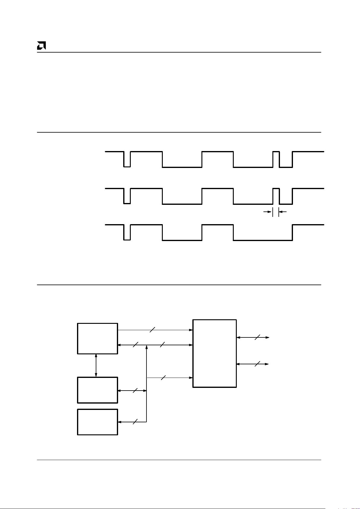
The patented GLITCH EATER Circuitry in the
Enhanced SCSI-2 Controller can be programmed to
filter glitches with widths up to 35 ns. It is designed to
dramatically increase system reliability by detecting and
removing glitches that may cause system failure. The
GLITCH EATER Circuitry is implemented on the ACK
and REQ lines since they are most susceptible to
electrical anomalies such as reflections and voltage
spikes. Such signal inconsistencies can trigger false
REQ/ACK handshaking, false data transfers, addition of
random data, and double clocking. AMD’s GLITCH
EATER Circuitry therefore maintains system performance and improves reliability. The following diagram
illustrates this circuit’s operation.
The Am53CF94 is also available in a 3.3 V version.
SCSI Environment
Device without the
GLITCH EATER Circuit
AMD’s Device with the
GLITCH EATER Circuit
GLITCH EATER Circuitry in SCSI Environment
Note:
The Glitch Window is programmable via Control Register Four (0DH), bits 6 & 7. Window may be set to 35 ns (max). Default
setting is 12 ns (single-ended).
17348B-1
Glitch Window
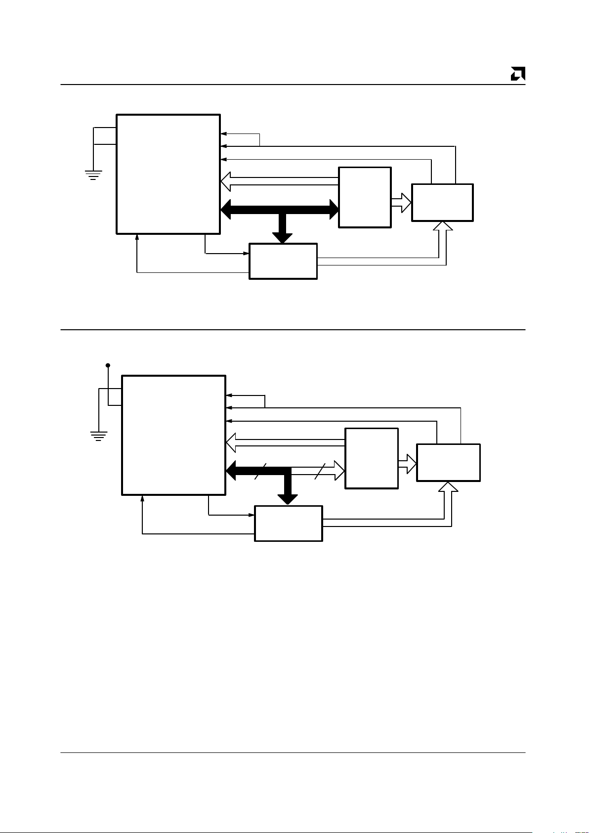
SYSTEM BLOCK DIAGRAM
9
CPU
DMA
Memory
Am53CF94/96
8
16
16
4
9
SCSI Data
16
DMA
Addr
Data
SCSI Control
16
17348B-2
P R E L I M I N A R Y AMD
3
Am53CF94/Am53CF96
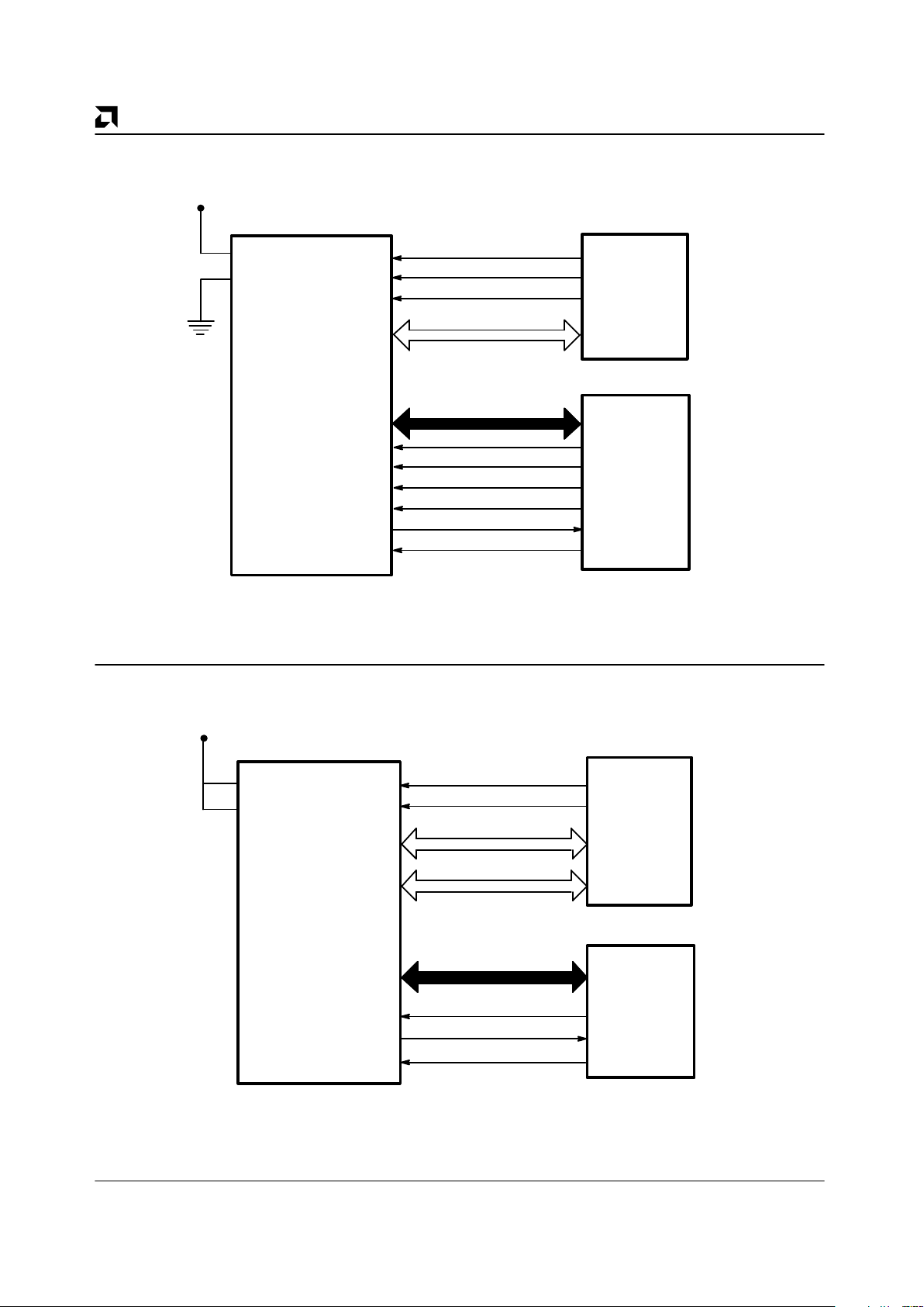
SYSTEM BUS MODE DIAGRAMS
8-Bit Data Bus
Address Bus
DMA
Controller
Host
Processor
Am53CF94/96
Bus
Controller
DMA 7–0
A 3–0
RD
WR
DMAWR
BUSMD 0
BUSMD 1
DREQ
DACK
Bus Mode 0
Single Bus Architecture: 8-Bit DMA, 8-Bit Processor
17348B-3
Data Bus
Address Bus
RD
WR
DMAWR
DREQ
DACK
DMA
Controller
Host
Processor
Am53CF94/96
Bus
Controller
DMA 15–0
A 3–0
BUSMD 0
BUSMD 1
8
16
V
DD
Bus Mode 1
Single Bus Architecture: 16-Bit DMA, 8-Bit Processor
17348B-4
P R E L I M I N A R YAMD
4 Am53CF94/Am53CF96
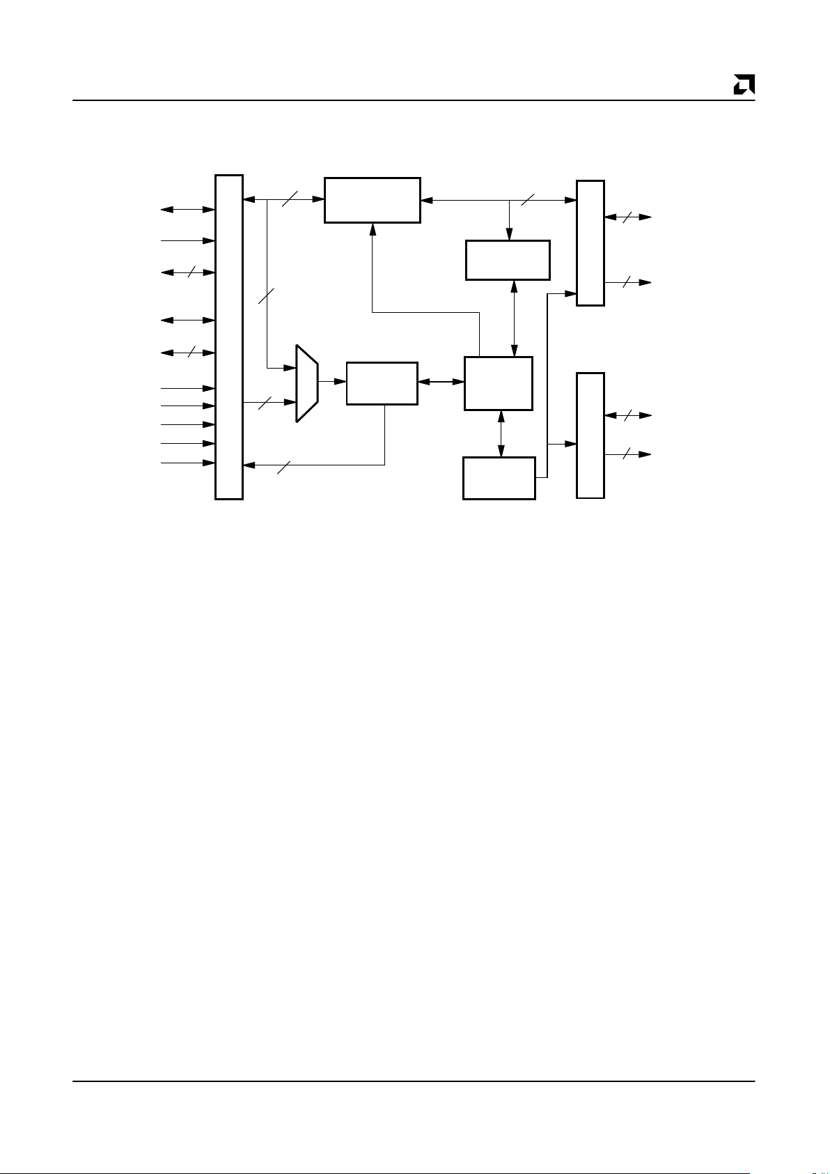
SYSTEM BUS MODE DIAGRAMS
DMARD
V
DD
8-Bit Data Bus
DMA
Controller
Host
Processor
Am53CF94/96
DMA 15–0
AD 7–0
WR
DMAWR
BUSMD 0
BUSMD 1
DREQ
DACK
RD
BHE
AS0
ALE
16-Bit Data Bus
Bus Mode 2
Dual Bus Architecture: 16-Bit DMA with Byte Control,
8-Bit Multiplexed Processor Address Data
17348B-5
V
DD
Address Bus
DMA
Controller
Host
Processor
Am53CF94/96
DMA 15–0
A 3–0
WR
DMAWR
BUSMD 0
BUSMD 1
DREQ
DACK
RD
16-Bit Data Bus
8-Bit Data Bus
AD 7–0
Bus Mode 3
Dual Bus Architecture: 16-Bit DMA,
8-Bit Processor
17348B-6
P R E L I M I N A R Y AMD
5
Am53CF94/Am53CF96
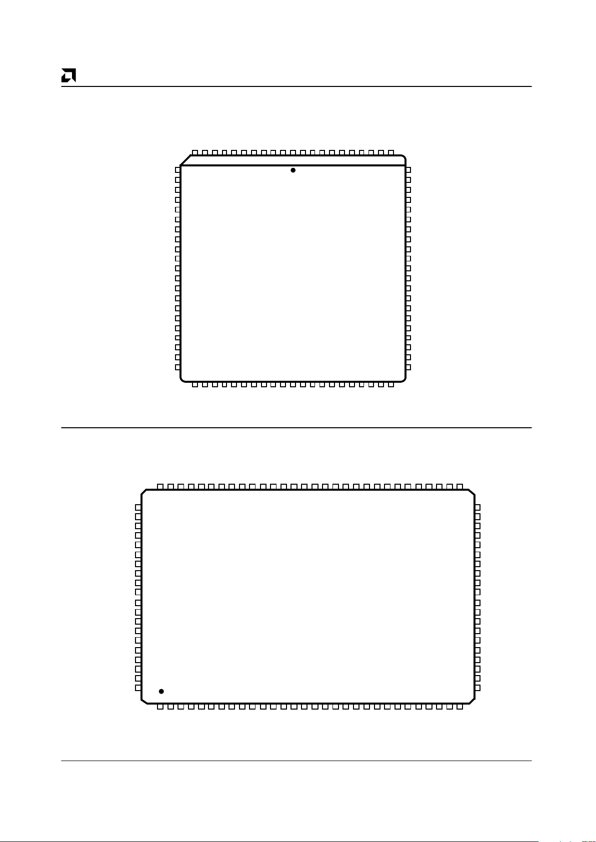
BLOCK DIAGRAM
17348B-7
Bus Interface Unit
18
18
16 x 9 FIFO
(including parity)
Parity Logic
Data Tranceivers
SCSI Control
MUX
8
8
8
9
CLK
6
4
DMA
15-0
DMAP
1-0
DMA Control
AD
7-0
Host Control
BUSMD
1-0
RESET
CS
9
SCSI Control
SCSI Bus
Data + Parity
(Single Ended)
Main
Sequencer
SCSI
Sequencer
Register
Bank
DFMODE
9
SCSI Bus
Data + Parity
Direction Control
7
SCSI Control
Direction Control
P R E L I M I N A R YAMD
6 Am53CF94/Am53CF96
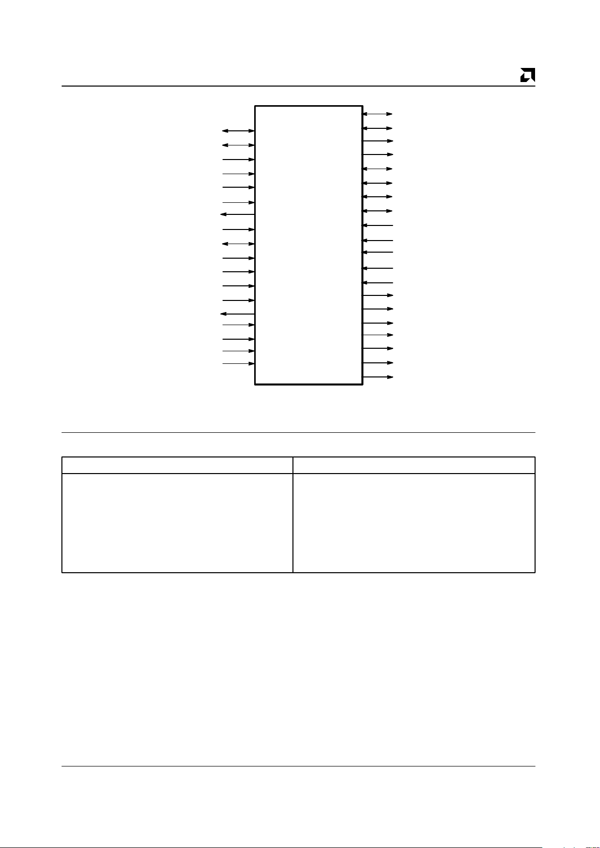
CONNECTION DIAGRAMS
Top View
17348B-8
DMA11
DMA10
DMA9
DMA8
DMA7
DMA3
DMA2
DMA1
DMA0
DMA4
DMAP0
DMAP1
DMA14
DMA13
DMA12
DMA15
DMA5
DMA6
AD3
AD2
AD1
AD0
CLK
ALE [A3]
DMARD [A2]
BHE [A1]
AS0 [A0]
AD4
AD5
DREQ
DACK
DMAWR
AD6
AD7
CS
RD
WR
BSYC
REQC
MSG
C/D
I/O
ATN
RSTC
SEL
BSY
REQ
ACK
RST
BUSMD 0
INT
RESET
SELC
BUSMD 1
ACKC
12
13
14
15
16
17
18
19
20
21
22
23
24
25
26
27
28
29
30
31
32
74
73
72
71
70
69
68
67
66
65
64
63
62
61
59
58
57
56
55
54
60
33 34 35 36 37 38 39 40 41 42 43 44 45 46 47 48 49 50 51 52 53
111098765432184838281807978777675
Am53CF94
84-Pin PLCC
SD6
SD7
SDP
V
DD
VSS
V
SS
SD3
SD4
SD5
SD0
SD1
SD2
SDC3
SDC0
SDC1
SDC2
SDC6
SDC7
SDCP
SDC4
SDC5
V
DD
V
SS
V
SS
V
SS
V
SS
V
SS
V
SS
V
SS
NC
ISEL
TSEL
DMA0
DMA1
DMA2
DMA3
DMA4
DMA5
DMA6
DMA7
DMAP0
DMA8
DMA9
DMA10
DMA11
DMA12
DMA13
DMA14
DMA15
DMAP1
NC
SD 0
SD 1
DACK
DMAWR
NC
SDC 7
SDC P
BUSMD 0
BUSMD 1
RST
ACK
REQ
SEL
ATN
I/O
C/D
MSG
ACKC
REQC
BSYC
V
SS
RSTC
BSY
RD
NC
RESET
INT
WR
SELC
V
SS
NC
SDC 6
CS
AS0 [A0]
BHE [A1]
DMARD [A2]
ALE [A3]
CLK
DFMODE
NC
AD0
AD1
AD2
AD3
V
SS
V
SS
AD4
AD5
AD6
AD7
DREQ
V
SS
V
SS
V
SS
V
SS
V
SS
V
SS
V
DD
V
DD
SDC 0
SDC 1
SDC 2
SDC 3
SDC 4
SDC 5
SD 2
SD 3
VSSV
SS
SD 4
SD 5
SD 6
SD 7
SD P
VSSV
SS
31
32
33
34
35
36
37
38
39
40
41
42
43
45
46
47
48
49
50
44
Am53CF96
100-Pin PQFP
100
99
98
97
96
95
94
93
92
91
90
89
88
87
86
85
84
83
82
81
29
1
23 45678910111213141516171819202122232425262728
30
52
80 79 78 77 76 75 74 73 72 71 70 69 68 67 66 65 64 63 62 61 60 59 58 57 56 55 54 53
51
VSSV
SS
17348B-9
P R E L I M I N A R Y AMD
7
Am53CF94/Am53CF96
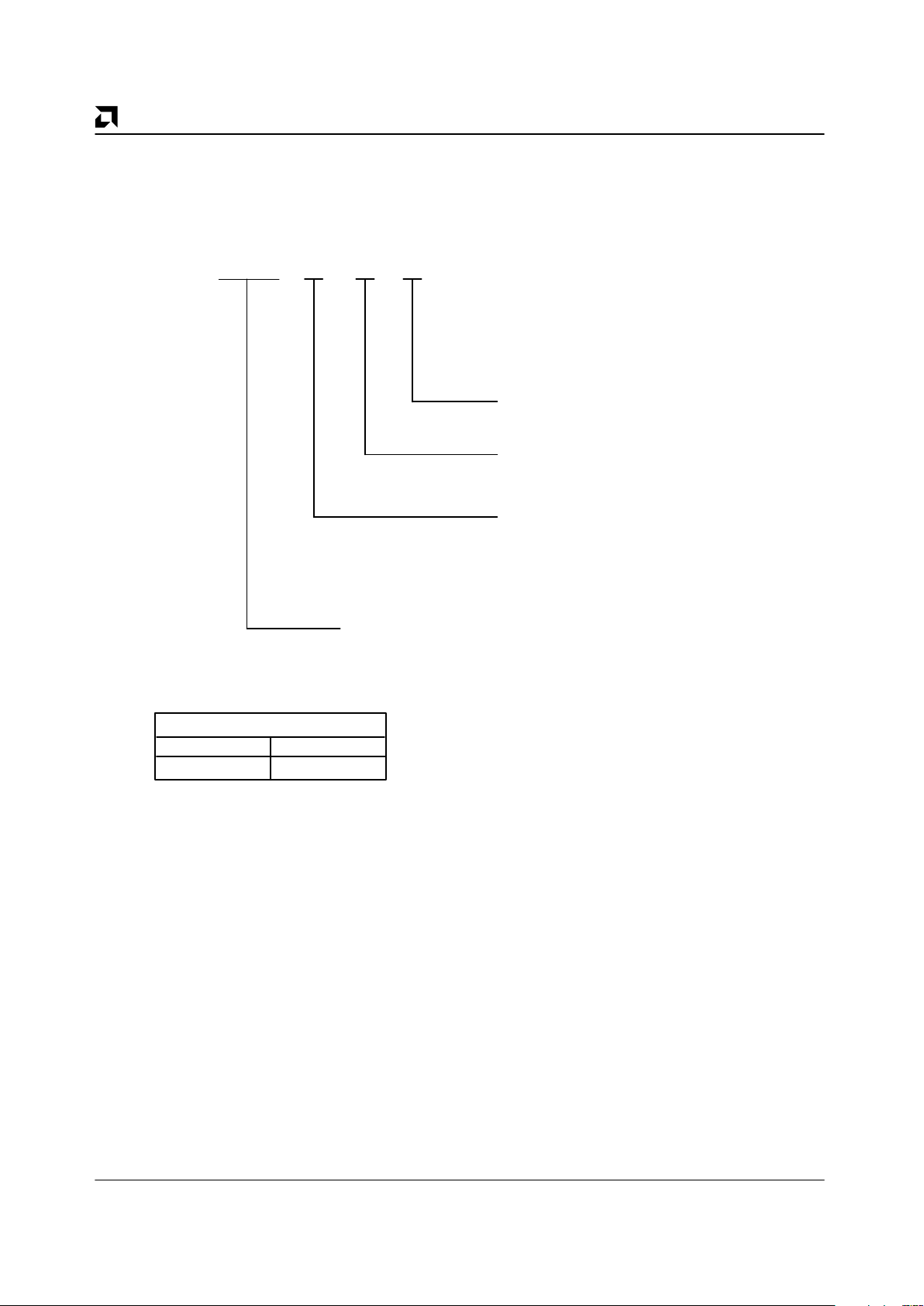
LOGIC SYMBOL
SDC P
BUSMD 1–0
*DFMODE
INT
CS
WR
RD
Am53CF94/96
SD 7–0
SD P
BSYC
MSG
C/D
I/O
ATN
SELC
RSTC
REQC
ACKC
SDC 7–0
BSY
SEL
RST
REQ
ACK
*ISEL
*TSEL
DMA 15–0
DMAP 1–0
DREQ
BHE [A1]
AS0 [A0]
ALE [A3]
AD 7–0
DMARD [A2]
DACK
DMAWR
CLK
RESET
Note:
*Pins available on the Am53CF96 only.
17348B-10
RELATED AMD PRODUCTS
Part Number Description
85C30 Enhanced Serial Communication
Controller
26LSXX Line Drivers/Receivers
33C93A Enhanced CMOS SCSI Bus
Interface Controller
80C186 Highly Integrated 16-Bit
Microprocessor
80C286 High-Performance 16-Bit
80286 Microprocessor
Part Number Description
Am386
TM
High-Performance 32-Bit
Microprocessor
53C80A SCSI Bus Controller
80188 Highly Integrated 8-Bit Microprocessor
85C80 Combination 53C80A SCSI and
85C30 ESCC
53C94LV Low Voltage, High Performance
SCSI Controller
P R E L I M I N A R YAMD
8 Am53CF94/Am53CF96
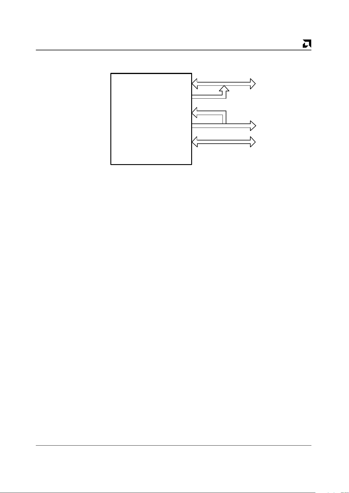
ORDERING INFORMATION
Standard Products
AMD standard products are available in several packages and operating ranges. The order number (Valid Combination) is
formed by a combination of:
TEMPERATURE RANGE
C = Commercial
PACKAGE TYPE
J = 84-Pin PLCC (PL 084)
K = 100-Pin Metric PQFP (PQR100)
DEVICE NUMBER/DESCRIPTION
Am53CF94/Am53CF96
Enhanced SCSI-2 Controller
AM53CF94
AM53CF96
AM53CF96 K C
Valid Combinations
Valid Combinations list configurations planned to be
supported in volume for this device. Consult the local AMD sales office to confirm availability of specific
valid combinations or to check on newly released
combinations.
JC
KC, KC/W
Valid Combinations
ALTERNATE PACKAGING OPTION
/W = Trimmed and Formed in a Tray
Blank = Molded Carrier Ring (36 mm)
/W
P R E L I M I N A R Y AMD
9
Am53CF94/Am53CF96
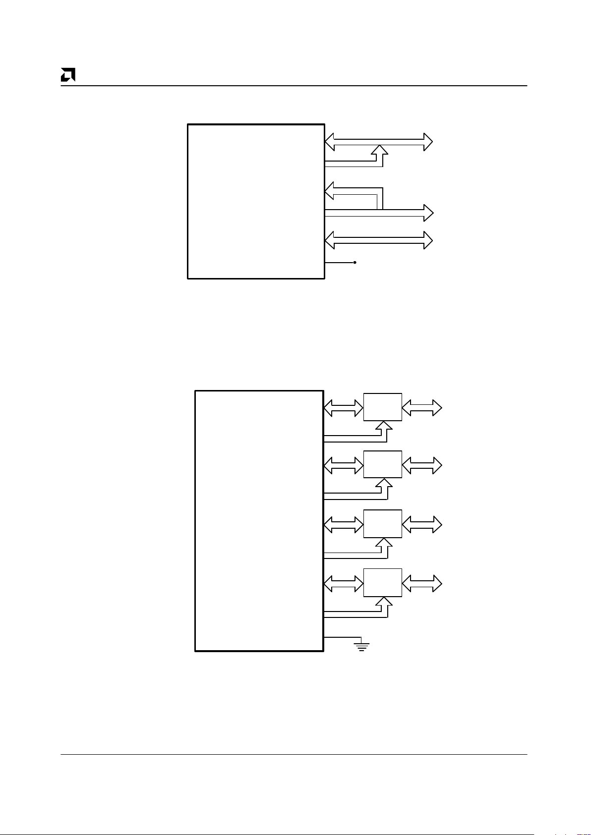
SCSI OUTPUT CONNECTIONS
Am53CF94
Am53CF94 Single Ended SCSI Bus Configuration
SDC 7–0, P
SELC, BSYC, REQC,
ACKC, RSTC
SD 7–0, P
SEL, BSY, REQ, ACK, RST
MSG, C/D, I/O, ATN
17348B-11
P R E L I M I N A R YAMD
10 Am53CF94/Am53CF96
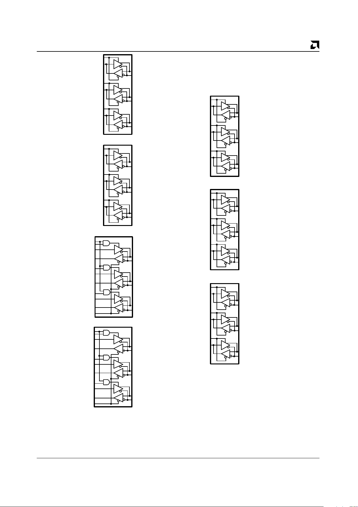
SCSI OUTPUT CONNECTIONS
Am53CF96
Am53CF96 Single Ended SCSI Bus Configuration
SDC 7–0, P
SELC, BSYC, REQC,
ACKC, RSTC
SD 7–0, P
SEL, BSY, REQ, ACK, RST
MSG, C/D, I/O, ATN
DFMODE
V
CC
17348B-12
SDC 7–0, P
SELC, BSYC, RSTC
SD 7–0, P
SEL, BSY, RST
MSG, C/D, I/O, REQ
DFMODE
ATN, ACK
Am53CF96 Differential SCSI Bus Configuration
TSEL
ISEL
Am53CF96
DT
DT
DT
DT
17348B-13
P R E L I M I N A R Y AMD
11
Am53CF94/Am53CF96
TSEL
Vcc
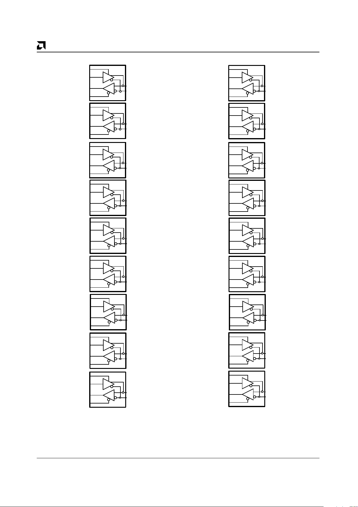
Differential Transceiver Connections for the Differential SCSI Bus Configuration
Using 75ALS170 and 75ALS171 Transceivers
Vcc
SELC
GND
SEL
+ SEL
– SEL
BSYC
GND
BSY
+ BSY
– BSY
RSTC
GND
RST
+ RST
– RST
GND
75ALS171
SDC 6
SD 6
– SD 6
+ SD 6
SDC 7
SD 7
– SD 7
+ SD 7
SDC P
SD P
– SD P
+ SD P
75ALS170
SDC 3
SD 3
– SD 3
+ SD 3
SDC 4
SD 4
– SD 4
+ SD 4
SDC 5
SD 5
– SD 5
+ SD 5
75ALS170
SDC 0
SD 0
– SD 0
+ SD 0
SDC 1
SD 1
– SD 1
+ SD 1
SDC 2
SD 2
– SD 2
+ SD 2
75ALS170
ATN
ISEL
– ATN
+ ATN
75ALS170
– MSG
+ MSG
– C/D
TSEL
MSG
TSEL
C/D
+ C/D
TSEL
I/O
– I/O
+ I/O
75ALS170
REQC
ACKC
REQ
+ REQ
– REQ
ISEL
ACK
+ ACK
– ACK
75ALS171
GND
17348B-14
P R E L I M I N A R YAMD
12 Am53CF94/Am53CF96
SDC 6
SD 6
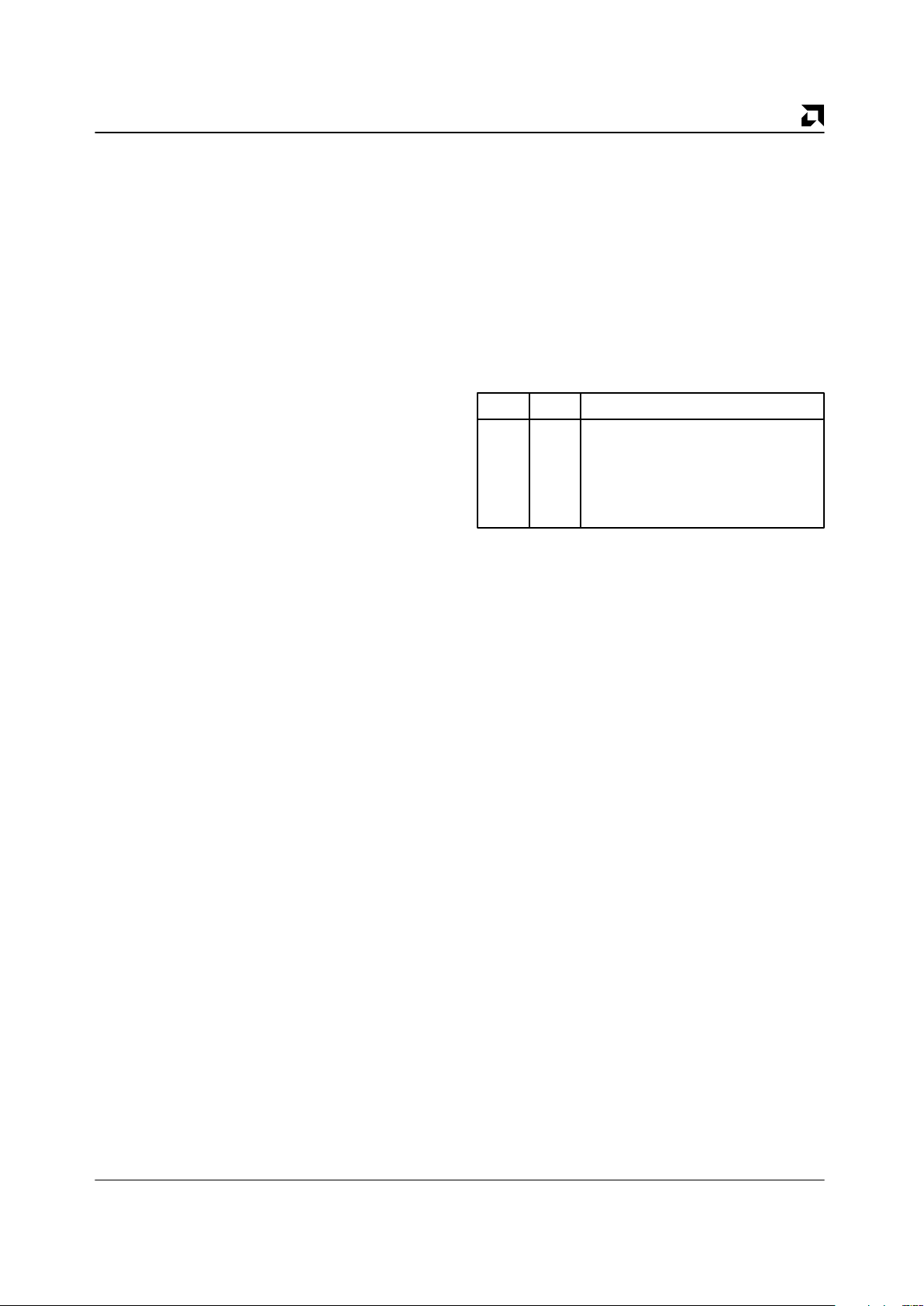
Differential Transceiver Connections for the Differential
SCSI Bus Configuration Using 75176A Transceiver
– SD 6
+ SD 6
SD 6
SDC 6
RSTC
GND
RST
+ RST
– RST
GND
SDC 0
SD 0
– SD 0
+ SD 0
SDC 0
SD 0
TSEL
MSG
– MSG
+ MSG
MSG
TSEL
SDC 1
SD 1
– SD 1
+ SD 1
SD 1
SDC 1
TSEL
C/D
– C/D
+ C/D
C/D
TSEL
SDC 2
SD 2
– SD 2
+ SD 2
SD 2
SDC 2
TSEL
I/O
– I/O
+ I/O
I/O
TSEL
SDC 3
SD 3
– SD 3
+ SD 3
SD 3
SDC 3
ISEL
ATN
– ATN
+ ATN
ATN
ISEL
SDC 4
SD 4
– SD 4
+ SD 4
SD 4
SDC 4
SELC
GND
SEL
+ SEL
– SEL
GND
SDC 5
SD 5
– SD 5
+ SD 5
SD 5
SDC 5
BSYC
GND
BSY
+ BSY
– BSY
GND
SDC 7
SD 7
– SD 7
+ SD 7
SD 7
SDC 7
TSEL
REQC
REQ
+ REQ
– REQ
GND
SDC P
SD P
– SD P
+ SD P
SD P
SDC P
ISEL
ACKC
ACK
+ ACK
– ACK
GND
17348B-15
P R E L I M I N A R Y AMD
13
Am53CF94/Am53CF96
PIN DESCRIPTION
Host Interface Signals
DMA 15–0
Data/DMA Bus
(Input/Output, Active High, Internal Pull-up)
The configuration of this bus depends on the Bus Mode
1–0 (BUSMD 1–0) inputs. When the device is configured for single bus operation, the host can access the
internal register set on the lower eight lines while DMA
accesses can be made to the FIFO using the entire bus.
When using the Byte Mode via the BHE and A0 inputs
the data can be transferred on either the upper or lower
half of the DMA 15–0 bus.
DMAP 1–0
Data/DMA Parity Bus
(Input/Output, Active High, Internal Pull-up)
These lines are odd parity for the DMA 15–0 bus. DMAP
1 is the parity for the upper half of the bus (DMA 15–8)
and DMAP 0 is the parity for the lower half of the bus
(DMA 7–0).
ALE [A3]
Address Latch Enable [Address 3]
(Input, Active High)
This is a dual function input. When the device is configured for the dual bus mode (two buses, multiplexed and
byte control), this input acts as ALE. As ALE, this input
latches the address on the AD 7–0 bus on its low going
edge. When the device is configured for all other bus
modes, this input acts as A3. As A3, this input is the third
bit of the address bus.
DMARD [A2]
DMA Read [Address 2]
(Input, Active Low [Active High])
This is a dual function input. When the device is configured for the dual bus mode (two buses, multiplexed and
byte control), this input acts as DMARD. As DMARD,
this input is the read signal for the DMA 15–0 bus. When
the device is configured for all other bus modes, this input acts as A2. As A2, this input is the second bit of the
address bus.
BHE [A1]
Bus High Enable [Address 1]
(Input, Active High)
This is a dual function input. When the device is configured for the dual bus mode (two buses, multiplexed and
byte control), this input acts as BHE. As BHE, this input
works in conjunction with AS0 to indicate the lines on
which data transfer will take place. When the device is
configured for all other bus modes this input acts as A1.
As A1, this input is the first bit of the address bus.
AS0 [A0]
Address Status [Address 0]
(Input, Active High)
This is a dual function input. When the device is configured for the dual bus mode (two buses, multiplexed and
byte control), this input acts as AS0. As AS0, this input
works in conjunction with BHE to indicate the lines on
which data transfer will take place. When the device is
configured for all other bus modes, this input acts as A0.
As A0, this input is the zeroth bit of the address bus.
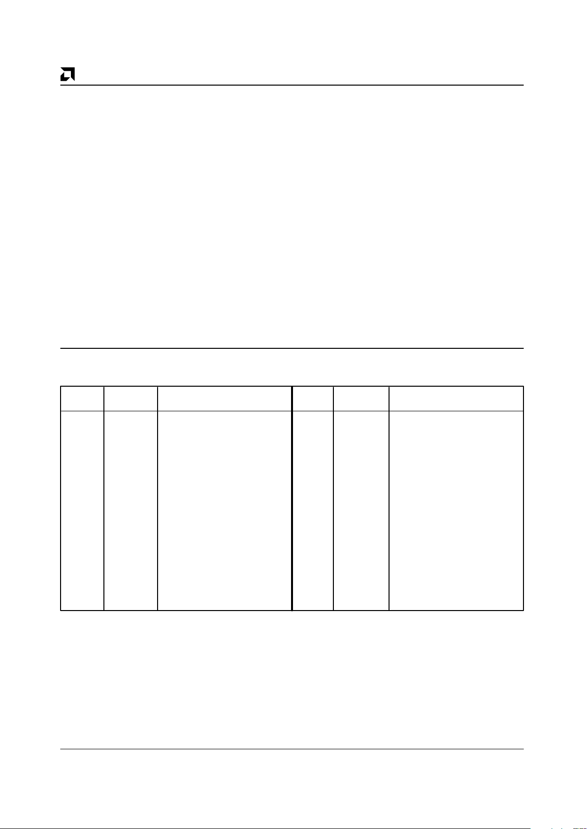
The following is the decoding for the BHE and AS0
inputs:
BHE AS0 Bus Used
1 1 Upper Bus – DMA 15–8, DMAP 1
1 0 Full Bus – DMA 15–0, DMAP 1–0
0 1 Reserved
0 0 Lower Bus – DMA 7–0, DMAP 0
DREQ
DMA Request
(Output, Active High, Hi-Z)
This output signal to the DMA controller will be active
during DMA read and write cycles. During a DMA read
cycle it will be active as long as there is a word (or a byte
in the byte mode) in the FIFO to be transferred to memory. During a DMA write cycle it will be active as long as
there is an empty space for a word (or a byte in mode 2)
in the FIFO.
DACK
DMA Acknowledge
(Input, Active Low)
This input signal from the DMA controller will be active
during DMA read and write cycles. The DACK signal is
used to access the DMA FIFO only and should never be
active simultaneously with the CS signal, which accesses the registers only.
AD 7–0
Host Address Data Bus
(Input/Output, Active High, Internal Pull-up)
This bus is used only in the dual bus mode. This bus allows the host processor to access the device’s internal
registers while the DMA bus is transferring data. When
using multiplexed bus, these lines can be used for address and data. When using non multiplexed bus these
lines can be used for the data only.
P R E L I M I N A R YAMD
14 Am53CF94/Am53CF96
DMAWR
DMA Write
(Input, Active Low)
This signal writes the data onto the DMA 15–0 and
DMAP 1–0 bus into the internal FIFO when DACK is
also active. When in the single bus mode this signal
must be tied to the WR signal.
RD
Read
(Input Active Low)
This signal reads the internal device registers and
places their contents on the data bus, when either CS
signal or DACK signal is active.
WR
Write
(Input Active Low)
This signal writes the internal device registers with the
value present on the (AD 7–0 bus or the DMA 15–0 and
DMAP 1–0 bus), when the CS signal is also active.
CS
Chip Select
(Input Active Low)
This signal enables the read and write of the device registers. CS enables access to any register (including the
FIFO) while the DACK enables access only to the FIFO.
CS and DACK should never be active simultaneously in
the single bus mode, they may however be active simultaneously in the dual bus mode provided the CS signal is
not enabling access to the FIFO.
INT
Interrupt
(Output, Active Low, Open Drain)
This signal is a non-maskable interrupt flag to the host
processor. This signal is latched on the output on the
high going edge of the clock. This flag may be cleared by
reading the Interrupt Status Register (ISTAT) or by performing a device reset (hard or soft). This flag is not
cleared by a SCSI reset.
DFMODE
Differential Mode
(Input, Active Low)
This input is available only on the Am53CF96. This input
configures the SCSI bus to either single ended or differential mode. When this input is active, the device operates in the differential SCSI mode. The SCSI data is
available on the SD 7–0 lines and the high active transceiver enables on the SDC 7–0 outputs. When this input
is inactive, the device operates in the single ended SCSI
mode. The SCSI input data is available on SD 7–0 lines
and the output data is available on SDC 7–0 lines. In the
single ended SCSI mode, the SD 7–0 and the SDC 7–0
buses can be tied together externally.
BUSMD 1–0
Bus Mode
(Input, Active High)
These inputs configure the device for single bus or dual
bus operation and the DMA bus width.
BUSMD1 BUSMD0 Bus Configuration
1 1 Two buses: 8-bit Host Bus
and 16-bit DMA Bus
Register Address on A 3–0
and Data on AD Bus
1 0 Two buses: Multiplexed
and byte control
Register Address on AD 3–0
and Data on AD Bus
0 1 Single bus: 8-bit Host Bus
and 16-bit DMA Bus
Register Address on A 3–0
and Data on DMA Bus
0 0 Single bus: 8-bit Host Bus
and 8-bit DMA Bus
Register Address on A 3–0
and Data on DMA Bus
CLK
Clock
(Input)
Clock input used to generate all the internal device timings. The maximum frequency of this input is 40 MHz.
and a minimum of 10 MHz to maintain the SCSI bus
timings.
RESET
Reset
(Input, Active High)
This input when active resets the device. The RESET input must be active for at least two CLK periods after the
voltage on the power inputs have reached Vcc
minimum.
SCSI Interface Signals
SD 7–0
SCSI Data
(Input/Output, Active Low, Schmitt Trigger)
When the device is configured in the Single Ended SCSI
Mode (DFMODE inactive) these pins are defined as inputs for the SCSI data bus. When the device is configured in the Differential SCSI Mode (DFMODE active)
these pins are defined as bidirectional SCSI data bus.

P R E L I M I N A R Y AMD
15
Am53CF94/Am53CF96
SD P
SCSI Data Parity
(Input/Output, Active Low, Schmitt Trigger)
When the device is configured in the Single Ended SCSI
Mode (DFMODE inactive) this pin is defined as the input
for the SCSI data parity. When the device is configured
in the Differential SCSI Mode (DFMODE active) this pin
is defined as bidirectional SCSI data parity.
SDC 7–0
SCSI Data Control
(Output, Active Low, Open Drain)
When the device is configured in the Single Ended SCSI
Mode (DFMODE inactive) these pins are defined as outputs for the SCSI data bus. When the device is configured in the Differential SCSI Mode (DFMODE active)
these pins are defined as direction controls for the external differential transceivers. In this mode, a signal high
state corresponds to an output to the SCSI bus and a
low state corresponds to an input from the SCSI bus.
SDC P
SCSI Data Control Parity
(Output, Active Low, Open Drain)
When the device is configured in the Single Ended SCSI
Mode (DFMODE inactive) this pin is defined as an output for the SCSI data parity. When the device is configured in the Differential SCSI Mode (DFMODE active)
this pin is defined as the direction control for the external
differential transceiver. In this mode, a signal high state
corresponds to an output to the SCSI bus and a low
state corresponds to an input from the SCSI bus.
MSG
Message
(Input/Output, Active Low, Schmitt Trigger)
This is a bidirectional signal with 48 mA output driver.
It is an output in the Target mode and a Schmitt trigger
input in the Initiator mode.
C/D
Command/Data
(Input/Output, Schmitt Trigger)
This is a bidirectional signal with 48 mA output driver.
It is an output in the Target mode and a Schmitt trigger
input in the Initiator mode.
I/O
Input/Output
(Input/Output, Schmitt Trigger)
This is a bidirectional signal with 48 mA output driver.
It is an output in the Target mode and a Schmitt trigger
input in the Initiator mode.
ATN
Attention
(Input/Output, Active Low, Schmitt Trigger)
This signal is a 48 mA output in the Initiator mode and a
Schmitt trigger input in the Target mode. This signal will
be asserted when the Initiator detects a parity error or it
can be asserted via certain Initiator commands.
BSY
Busy
(Input, Active Low, Schmitt Trigger)
This is a SCSI input signal with a Schmitt trigger.
SEL
Select
(Input, Active Low, Schmitt Trigger)
This is a SCSI input signal with a Schmitt trigger.
RST
Reset
(Input, Active Low, Schmitt Trigger)
This is a SCSI input signal with a Schmitt trigger.
REQ
Request
(Input, Active Low, Schmitt Trigger)
This is a SCSI input signal with a Schmitt trigger.
ACK
Acknowledge
(Input, Active Low, Schmitt Trigger)
This is a SCSI input signal with a Schmitt trigger.
BSYC
Busy Control
(Output, Active Low, Open Drain)
This is a SCSI output with 48 mA drive. When the device
is configured in the Single Ended SCSI Mode (DFMODE
inactive) this pin is defined as a BSY output for the SCSI
bus. When the device is configured in the Differential
SCSI Mode (DFMODE active) this pin is defined as the
direction control for the external differential transceiver.
In this mode, a signal high state corresponds to an output to the SCSI bus and a low state corresponds to an
input from the SCSI bus.
SELC
Select Control
(Output, Active Low, Open Drain)
This is a SCSI output with 48 mA drive. When the device
is configured in the Single Ended SCSI Mode (DFMODE
inactive) this pin is defined as a SEL output for the SCSI
bus. When the device is configured in the Differential
SCSI Mode (DFMODE active) this pin is defined as the
direction control for the external differential transceiver.
In this mode, a signal high state corresponds to an output to the SCSI bus and a low state corresponds to an
input from the SCSI bus.
P R E L I M I N A R YAMD
16 Am53CF94/Am53CF96
RSTC
Reset Control
(Output, Active Low, Open Drain)
This is a SCSI output with 48 mA drive. The Reset SCSI
command will cause the device to drive RSTC active for
25 ms–40 ms, which will depend on the CLK frequency
and the conversion factor. When the device is configured in the Single Ended SCSI Mode (DFMODE inactive) this pin is defined as a RST output for the SCSI bus.
When the device is configured in the Differential SCSI
Mode (DFMODE active) this pin is defined as the direction control for the external differential transceiver. In
this mode, a signal high state corresponds to an output
to the SCSI bus and a low state corresponds to an input
from the SCSI bus.
REQC
Request Control
(Output, Active Low, Open Drain)
This is a SCSI output with 48 mA drive. This signal is
activated only in the Target mode.
ACKC
Acknowledge Control
(Output, Active Low, Open Drain)
This is a SCSI output with 48 mA drive. This signal is activated only in the Initiator mode.
ISEL
Initiator Select
(Output, Active High)
This signal is available on the Am53CF96 only. This signal is active whenever the device is in the Initiator mode.
In the differential mode this signal is used to enable the
Initiator signals ACKC and ATN and the device also
drives these signals.
TSEL
Target Select
(Output, Active High)
This signal is available on the Am53CF96 only. This signal is active whenever the device is in the Target mode.
In the differential mode this signal is used to enable the
Target signals REQC, MSG, C/D and I/O and the device
also drives these signals.
FUNCTIONAL DESCRIPTION
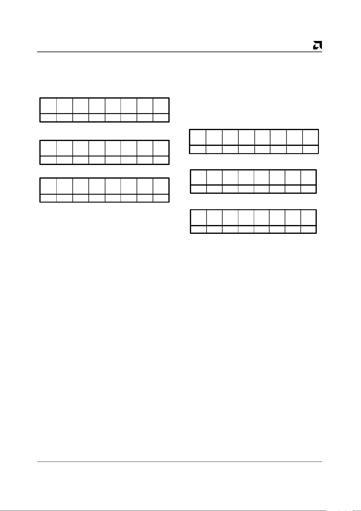
Register Map
Address
(Hex.) Operation Register
00 Read Current Transfer Count
Register Low
00 Write Start Transfer Count Register
Low
01 Read Current Transfer Count
Register Middle
01 Write Start Transfer Count Register
Middle
02 Read/Write FIFO Register
03 Read/Write Command Register
04 Read Status Register
04 Write SCSI Destination ID Register
05 Read Interrupt Status Register
05 Write SCSI Timeout Register
06 Read Internal State Register
06 Write Synchronous Transfer Period
Register
Address
(Hex.) Operation Register
07 Read Current FIFO/Internal State
Register
07 Write Synchronous Offset Register
08 Read/Write Control Register 1
09 Write Clock Factor Register
0A Write Forced Test Mode Register
0B Read/Write Control Register 2
0C Read/Write Control Register 3
0D Read/Write Control Register 4
0E Read Current Transfer Count
Register High
0E Write Start Transfer Count
Register High
0F Write Data Alignment Register
Note:
Not all registers in this device are both readable and writable. Some read only registers share the same address with write only
registers. The registers can be accessed by asserting the
CS
signal and then asserting either
RD
or WR signal depending on the
operation to be performed. Only the FIFO Register can be accessed by asserting either
CS
or
DACK
in conjunction with RD and
WR
signals or
DMARD
and
DMAWR
signals. The register address inputs are ignored when
DACK
is used but must be valid
when
CS
is used.
P R E L I M I N A R Y AMD
17
Am53CF94/Am53CF96
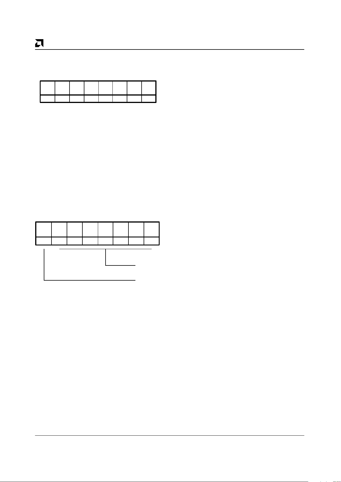
Current Transfer Count Register
(00H, 01H, 0EH) Read Only
Current Transfer Count Register
CTCREG
Address: 00H, 01H, 0EH
Type: Read
15 14 13 12 11 10 9 8
CRVL15 CRVL14 CRVL13 CRVL12 CRVL11 CRVL10 CRVL9 CRVL8
xxxxxxxx
76543210
CRVL7 CRVL6 CRVL5 CRVL4 CRVL3 CRVL2 CRVL1 CRVL0
xxxxxxxx
23 22 21 20 19 18 17 16
CRVL23 CRVL22 CRVL21 CRVL20 CRVL19 CRVL18 CRVL17 CRVL16
xxxxxxxx
17348B-16
CTCREG – Bits 23:0 – CRVL 23:0 – Current
Value 23:0
This is a three-byte register which decrements to keep
track of the number of bytes transferred during a DMA
transfer. Reading these registers returns the current
value of the counter. The counter will decrement by one
for every byte and by two for every word transferred. The
transaction is complete when the count reaches zero,
and bit 4 of the Status Register (04H) is set. Should the
sequence terminate early, the sum of the values in the
Current FIFO (07H) and the Current Transfer Count
Register reflect the number of bytes remaining.
The least significant byte is located at address 00H, the
middle byte is located at address 01H, and the most significant byte is located at address 0EH. Register 0EH
extends the total width of the register from 16 to 24
bits, and is only enabled when the Enable Features
bit (bit 6) of Control Register Two is set to a value
of ‘1’.
These registers are automatically loaded with the values in the Start Transfer Count Register every time a
DMA command is issued. However, following a chip or
power on reset, up until the time register 0EH is loaded,
the Am53CF94/96’s part-unique ID can be obtained by
reading register 0EH.
In the Target mode, this counter is decremented by the
active edge of DACK during the Data-In phase and by
REQC during the Data-Out phase.
In the Initiator mode, the counter is decremented by the
active edge of DACK during the Synchronous Data-In
phase or by ACKC during the Asynchronous Data-In
phase and by DACK during the Data-Out phase.
Start Transfer Count Register
(00H, 01H, 0EH) Write Only
Start Transfer Count Register
STCREG
Address: 00H–01H
Type: Write
15 14 13 12 11 10 9 8
STVL15 STVL14 STVL13 STVL12 STVL11 STVL10 STVL9 STVL8
xxxxxxxx
76543210
STVL7 STVL6 STVL5 STVL4 STVL3 STVL2 STVL1 STVL0
xxxxxxxx
23 22 21 20 19 18 17 16
STVL23 STVL22 STVL21 STVL20 STVL19 STVL18 STVL17 STVL16
xxxxxxxx
17348B-17
STCREG – Bits 15:0 – STVL 15:0 – Start Value 15:0
This is a three-byte register which contains the number
of bytes to be transferred during a DMA operation. The
value in the Start Transfer Count Register must be programmed prior to command execution.
The least significant byte is located at address 00H, the
middle byte is located at address 01H, and the most significant byte is located at address 0EH. Register 0EH
extends the total width of the register from 16 to 24 bits,
and is only enabled when the Enable Features bit (bit 6)
of Control Register Two is set to a value of ‘1’. This sets
the maximum transfer count to 16.78 MBytes. When a
value of ‘0’ is written to these registers, the transfer
count will be set to the maximum. A DMA NOP command must be issued before the transfer counter values
can be written to 00H, 01H, and 0EH.
These registers retain their value until overwritten, and
are therefore unaffected by a hardware or software reset. This reduces programming redundancy since it is
no longer necessary to reprogram the count for subsequent DMA transfers of the same size.
P R E L I M I N A R YAMD
18 Am53CF94/Am53CF96
FIFO Register (02H) Read/Write
FIFO Register
FFREG
Address: 02H
Type: Read/Write
76543210
FF7 FF6 FF5 FF4 FF3 FF2 FF1 FF0
00000000
17348B-18
FFREG – Bits 7:0 – FF 7:0 – FIFO 7:0
The FIFO on the Am53CF94/96 is 16 bytes deep and is
used to transfer SCSI data to and from the ESC. The
bottom of the FIFO may be accessed via a read or write
to this register. This is the only register that can also be
accessed by DACK along with DMARD or DMAWR or
with REQ or ACK. This register is reset to zero by hardware or software reset, or at the start of a selection or
reselection sequence, or if Clear FIFO command is
issued.
Command Register (03H) Read/Write
Command Register
CMDREG
Address: 03H
Type: Read/Write
76543210
DMA CMD6 CMD5 CMD4 CMD3 CMD2 CMD1 CMD0
xxxxxxxx
Command 6:0
Direct Memory
Access
17348B-19
Commands to the ESC are issued by writing to this register which is two bytes deep. Commands may be
queued, and will be read from the bottom of the queue.
At the completion of the bottom command, the top command, if present, will drop to the bottom of the register to
begin execution. All commands are executed within six
clock cycles of dropping to the bottom of the Command
Register, with the exception of the Reset SCSI Bus, Reset Device, and DMA Stop commands. These commands are not queued and are executed within four
clock cycles of being loaded into the top this register.
Interrupts are sometimes generated upon command
completion. Should both commands generate interrupts, and the first interrupt has not been serviced, the
interrupt from the second (top) command will be stacked
behind the first. The Status Register, Interrupt Register,
and Internal State Register will be updated to apply to
the second interrupt after the microprocessor services
the first interrupt.
Reading this register will return the command currently
being executed (or the last command executed if there
are no pending commands). When this register is
cleared, existing commands will be terminated and any
queued commands will be ignored. However, it does not
reset the register bits to ‘00H’.
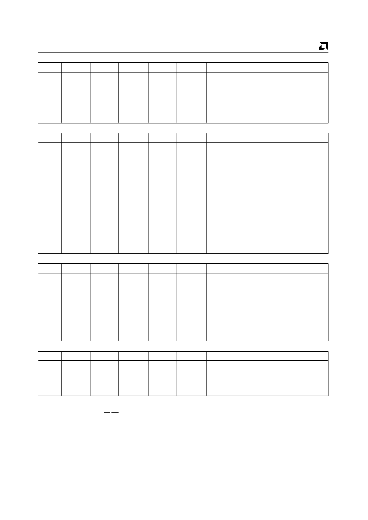
CMDREG – Bit 7 – DMA – Direct Memory Access
When set, this bit notifies the device that the command
is a DMA instruction, when reset it is a non-DMA instruction. For DMA instructions the Current Transfer Count
Register (CTCREG) will be loaded with the contents of
the Start Transfer Count Register (STCREG). The data
is then transferred and the CTCREG is decremented for
each byte until it reaches zero.
CMDREG – Bits 6:0 – CMD 6:0 – Command 6:0
These command bits decode the commands that the
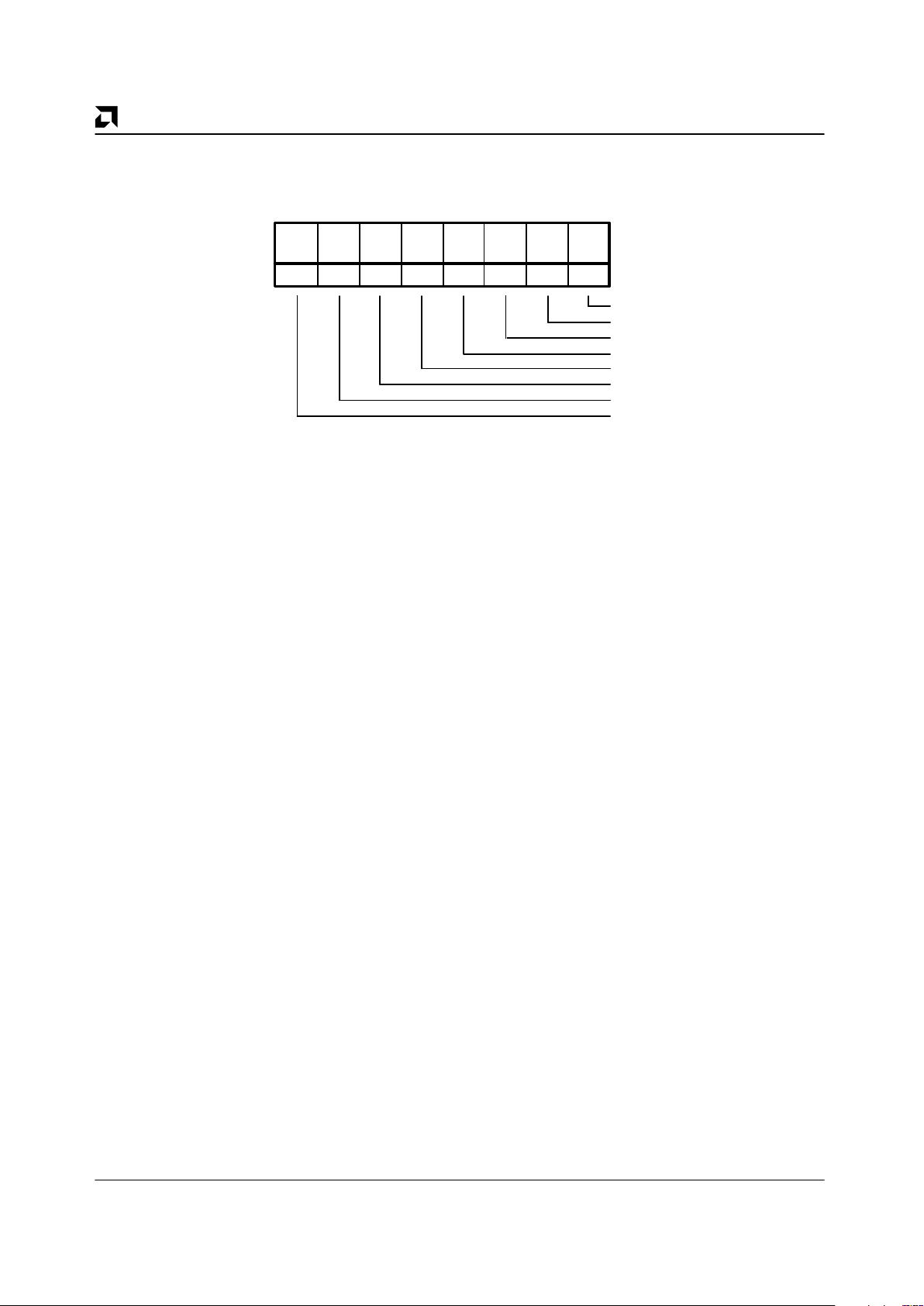
device needs to perform. There are a total of 31 commands grouped into four categories. The groups are
Initiator Commands, Target Commands, Selection/
Reselection Commands and General Purpose Commands.
P R E L I M I N A R Y AMD
19
Am53CF94/Am53CF96
Initiator Commands
CMD6 CMD5 CMD4 CMD3 CMD2 CMD1 CMD0 Command
0010000Information Transfer
00100 01Initiator Command Complete Steps
0010010Message Accepted
0011000Transfer Pad Bytes
0011010*Set ATN
0011011*Reset ATN
CMD6 CMD5 CMD4 CMD3 CMD2 CMD1 CMD0 Command
0100000Send Message
0100001Send Status
0100010Send Data
0100011Disconnect Steps
0100100Terminate Steps
0100101Target Command Complete Steps
0100111*Disconnect
0101000Receive Message Steps
0101001Receive Command
0101010Receive Data
0101011Receive Command Steps
0000100*DMA Stop
0000101Access FIFO Command
Idle Commands
CMD6 CMD5 CMD4 CMD3 CMD2 CMD1 CMD0 Command
1000000Reselect Steps
10000 01Select without ATN Steps
1000010Select with ATN Steps
1000011Select with ATN and Stop Steps
1000100*Enable Selection/Reselection
1000101Disable Selection/Reselection
1000110Select with ATN3 Steps
1000111Reselect with ATN3 Steps
General Commands
CMD6 CMD5 CMD4 CMD3 CMD2 CMD1 CMD0 Command
0000000*No Operation
00000 01*Clear FIFO
0000010*Reset Device
0000011Reset SCSI Bus
Target Commands
Note:
*Denotes commands which do
not generate interrupts upon completion.
P R E L I M I N A R YAMD
20 Am53CF94/Am53CF96
Status Register (04H) Read
Status Register
STATREG
Address: 04H
Type: Read
76543210
INT IOE PE CTZ GCV MSG C/D I/O
0000 0 xxx
Illegal Operation Error
Parity Error
Count to Zero
Group Code Valid
Message
Command/Data
Input/Output
Interrupt
17348B-20
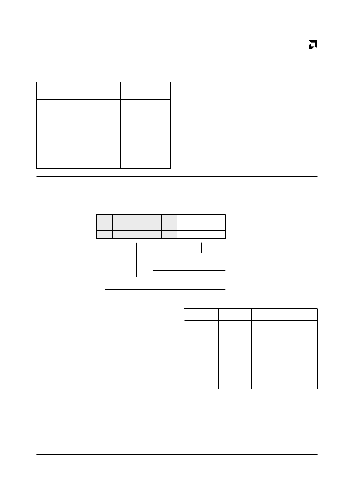
This read only register contains flags to indicate the
status and phase of the SCSI transactions. It indicates
whether an interrupt or error condition exists. It should
be read every time the host is interrupted to determine
which device is asserting an interrupt. If the ENF bit is
set (CNTLREG2, bit 6), the SCSI bus phase of the last
complete command (preceding the interrupt) will be
latched until the Interrupt Status Register (INSTREG) is
read. If the ENF bit is disabled, this register will reflect
the current bus phase. If command stacking is used, two
interrupts might occur. Reading this register will clear
the status information for the first interrupt and update
the Status Register for the second interrupt.
STATREG – Bit 7 – INT – Interrupt
The INT bit is set when the device asserts the interrupt
output. This bit will be cleared by a hardware or software
reset. Reading the Interrupt Status Register (INSTREG)
will deassert the interrupt output and also clear this bit.
STATREG – Bit 6 – IOE – Illegal Operation Error
The IOE bit is set when an illegal operation is attempted.
This condition will not cause an interrupt, it will be detected by reading the Status Register (STATREG) while
servicing another interrupt. The following conditions will
cause the IOE bit to be set:
■ DMA and SCSI transfer directions are opposite.
■ FIFO overflows or data is overwritten.
■ In Initiator mode an unexpected phase change
detected during synchronous data transfer.
■ Command Register overwritten.
This bit will be cleared by reading the Interrupt Status
Register (INSTREG) or by a hard or soft reset.
STATREG – Bit 5 – PE – Parity Error
The PE bit is set if any of the parity checking options are
enabled and the device detects a parity error on bytes
sent or received on the SCSI Bus. Parity options are
controlled by bits 5:4 in Control Register One
(CNTLREG1), and by bits 2:0 in Control Register Two
(CNTLREG2). The combination of enabled options will
determine if parity is generated from the data bytes
internally by the chip, or if it is passed between buffer
and SCSI Bus without being altered. Detection of a
parity error condition will not cause an interrupt but will
be reported with other interrupt causing conditions.
This bit will be cleared by reading the Interrupt Status
Register (INSTREG) or by a hard or soft reset.
STATREG – Bit 4 – CTZ – Count To Zero
The CTZ bit is set when the Current Transfer Count
Register (CTCREG) has counted down to zero. This bit
will be reset when the CTCREG is written with a nonzero value.
Reading the Interrupt Status Register (INSTREG) will
not affect this bit. This bit will however be cleared by a
hard or soft reset.
Note:
A non-DMA NOP will not reset the CTZ bit since it does
not load the CTCREG. However, a DMA NOP will reset
this bit since it loads the CTCREG.
STATREG – Bit 3 – GCV – Group Code Valid
The GCV bit is set if the group code field in the Command Descriptor Block (CDB) is one that is defined by
the ANSI Committee in their document X3.131 – 1986. If
the SCSI-2 Feature Enable (S2FE) bit in the Control
Register 2 (CNTLREG2) is set, Group 2 commands will
be treated as ten byte commands and the GCV bit will be
set. If S2FE is reset then Group 2 commands will be
treated as reserved commands. Group 3 and 4 commands will always be considered reserved commands.
The device will treat all reserved commands as six byte
commands. Group 6 commands will always be treated
as vendor unique six byte commands and Group 7 commands will always be treated as vendor unique ten byte
commands.
The GCV bit is cleared by reading the Interrupt Status
Register (INSTREG) or by a hard or soft reset.
P R E L I M I N A R Y AMD
21
Am53CF94/Am53CF96
STATREG – Bit 2 – MSG – Message
STATREG – Bit 1 – C/D – Command/Data
STATREG – Bit 0 – I/O – Input/Output
Bit2 Bit1 Bit0
MSG C/D I/O SCSI Phase
1 1 1 Message In
1 1 0 Message Out
1 0 1 Reserved
1 0 0 Reserved
0 1 1 Status
0 1 0 Command
0 0 1 Data_In
0 0 0 Data_Out
The MSG, C/D and I/O bits together can be referred to
as the SCSI Phase bits. They indicate the phase of the
SCSI bus. These bits may be latched or unlatched
depending on whether or not the ENF bit in Control
Register Two is set.
In the latched mode the SCSI phase bits are latched at
the end of a command and the latch is opened when the
Interrupt Status Register (INSTREG) is read. In the unlatched mode, they indicate the phase of the SCSI bus
when this register is read.
SCSI Destination ID Register (04H) Write
RES RES RES RES RES
00000
SCSI Destination ID Register
SDIDREG
Address: 04H
Type: Write
76543210
DID2 DID1 DID0
xxx
Reserved
Reserved
Reserved
Reserved
SCSI Destination ID 2:0
Reserved
17348B-21
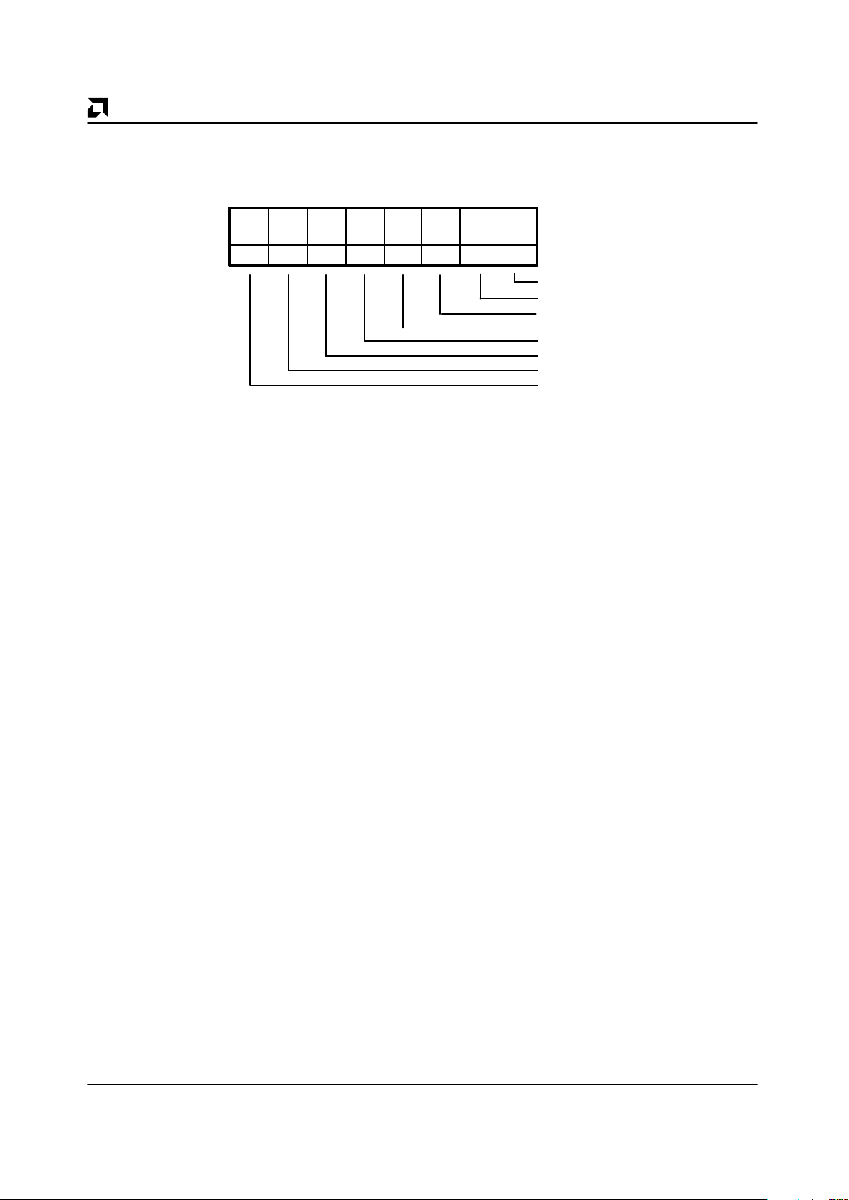
SDIDREG – Bits 7:3 – RES – Reserved
SDIDREG – Bits 2:0 – DID 2:0 – Destination ID 2:0
The DID 2:0 bits are the encoded SCSI ID of the device
on the SCSI bus which needs to be selected or
reselected.
At power-up the state of these bits is undefined. The DID
2:0 bits are not affected by reset.
DID2 DID1 DID0 SCSI ID
1117
1106
1015
1004
0113
0102
0011
0000
P R E L I M I N A R YAMD
22 Am53CF94/Am53CF96
Interrupt Status Register (05H) Read
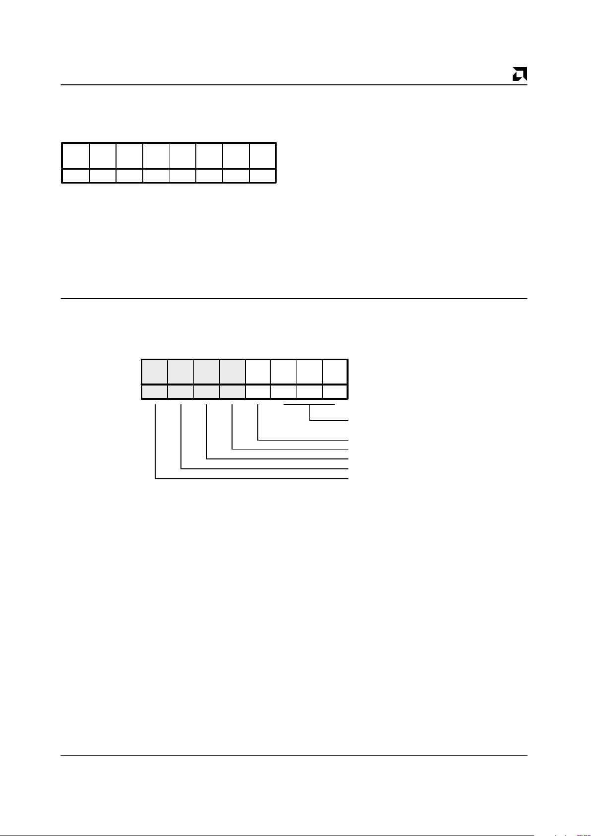
SRST ICMD DIS SR SO
00000
Interrupt Status Register
INSTREG
Address: 05h
Type: READ
76543210
RESEL SELA SEL
000
Invalid Command
Disconnected
Service Request
Successful Operation
Selected with Attention
SCSI Reset
Selected
Reselected
17348B-22
The Interrupt Status Register (INSTREG) will indicate
the reason for the interrupt. This register is used with the
Status Register (STATREG) and Internal State Register
(ISREG) to determine the reason for the interrupt.
Reading the INSTREG will clear all three registers.
Therefore the Status Register (STATREG) and Internal
State Register (ISREG) should be examined prior to
reading the INSTREG.
INSTREG – Bit 7 – SRST – SCSI Reset
The SRST bit will be set if a SCSI Reset is detected and
SCSI reset reporting is enabled via the DISR (bit 6) of
Control Register One (CNTLREG1).
INSTREG – Bit 6 – ICMD – Invalid Command
The ICMD bit will be set if the device detects an illegal
command code. This bit is also set if a command code is
detected from a mode that is different from the mode the
device is currently in. Once this bit is set, and invalid
command interrupt will be generated.
INSTREG – Bit 5 – DIS – Disconnected
The DIS bit can be set in the Target or the Initiator mode
when the device disconnects from the SCSI bus. In the
Target mode this bit will be set if a Terminate or a Command Complete steps causes the device to disconnect
from the SCSI bus. In the Initiator mode this bit will be
set if the Target disconnects; while in Idle mode, this bit
will be set if a selection or reselection timeout occurs.
INSTREG – Bit 4 – SR – Service Request
The SR bit can be set in the Target or the Initiator mode
when another device on the SCSI bus has a service
request. In the Target mode this bit will be set when the
Initiator asserts the ATN signal. In the Initiator mode this
bit is set when a Command Steps Successfully Completed Command is issued.
INSTREG – Bit 3 – SO – Successful Operation
The SO bit can be set in the Target or the Initiator mode
when an operation has successfully completed. In the
Target mode this bit will be set when any Target or Idle
state command is completed. In the Initiator mode this
bit is set after a Target has been successfully selected,
after a command has successfully completed and after
an information transfer command when the Target
requests a Message In phase.
INSTREG – Bit 2 – RESEL – Reselected
The RESEL bit is set at the end of the reselection phase
indicating that the device has been reselected as an
Initiator.
INSTREG – Bit 1 – SELA – Selected with Attention
The SELA bit is set at the end of the selection phase indicating that the device has been selected as a Target by
the Initiator and that the ATN signal was active during
the selection.
INSTREG – Bit 0 – SEL – Selected
The SEL bit is set at the end of the selection phase indicating that the device has been selected as a Target by
the Initiator and that the ATN signal was inactive during
the selection.
P R E L I M I N A R Y AMD
23
Am53CF94/Am53CF96
SCSI Timeout Register (05H) Write
SCSI Timeout Register
STIMREG
Address: 05H
Type: Write
76543210
STIM7 STIM6 STIM5 STIM4 STIM3 STIM2 STIM1 STIM0
xxxxxxxx
17348B-23
This register determines how long the Initiator (Target)
will wait for a response to a Selection (Reselection)
before timing out. It should be set to yield 250 ms to
comply with ANSI standards for SCSI, but the maximum
time out period may be calculated using the following
formulas.
Note: A hardware reset will clear this register.
STIMREG – Bits 7:0 – STIM 7:0 – SCSI Timer 7:0
The value loaded in STIM 7:0 can be calculated as
shown below:
STIM 7:0 =
[(SCSI Time Out) (Clock Frequency) / (8192 (Clock
Factor))]
Example:
SCSI Time Out (in seconds): 250 ms. (Recommended
by the ANSI Standard) = 250 x 10
–3 s.
Clock Frequency: 20 MHz. (assume) = 20 x 10
6 Hz.
Clock Factor: CLKF 2:0 from Clock Conversion Register
(09H) = 5
STIM 7:0 = (250 x 10
–3) X (20 x 106) / (8192 (5)) = 122
decimal
Internal State Register (06H) Read
Internal State Register
ISREG
Address: 06H
Type: Read
76543210
RES RES RES RES
SOF
IS2 IS1 IS0
xxxx 0 000
Reserved
Reserved
Reserved
Synchronous Offset Flag
Internal State 2:0
Reserved
17348B-24
The Internal State Register (ISREG) tracks the progress
of a sequence-type command. It is updated after each
successful completion of an intermediate operation. If
an error occurs, the host can read this register to
determine the point where the command failed and take
the necessary procedure for recovery. Reading the
Interrupt Status Register (INSTREG) while an interrupt
is pending will clear this register. A hard or soft reset will
also zero this register .
ISREG – Bits 7:4 – RES – Reserved
ISREG – Bit 3 – SOF – Synchronous Offset Flag
The SOF is reset when the Synchronous Offset Register
(SOFREG) has reached its maximum value.
Note:
The SOF bit is active Low.
ISREG – Bits 2:0 – IS 2:0 – Internal State 2:0
The IS 2:0 bits along with the Interrupt Status Register
(INSTREG) indicates the status of the successfully
completed intermediate operation. Refer to the Status
Decode section for more details.
 Loading...