AMD Advanced Micro Devices Am29SL800CT150WBIB, Am29SL800CT150WBI, Am29SL800CT150WBCB, Am29SL800CT150WBC, Am29SL800CT150FIB Datasheet
...
PRELIMINARY
Am29SL800C
8 Megabi t (1 M x 8-Bit/51 2 K x 16-Bit)
CMOS 1.8 Volt-only Super Low Volta ge Flash Memory
DISTINCTIVE CHARACTERISTICS
■ Single p ower supply operation
— 1.8 to 2.2 V for read, program, and erase
operations
— Ideal for battery-powered applications
■ Manufactured on 0.32 µm process technology
— Compatible with 0.35 µm Am29SL800B device
■ High performance
— Access times as fast as 100 ns
■ Ultra low power consumption (typical values at
5 MHz)
— 65 nA Automatic Sleep Mode current
— 65 nA standby mode current
— 5 mA read current
— 10 mA program/erase current
■ Flexible sector architecture
— One 16 Kbyte, two 8 Kbyte, one 32 Kbyte, and
fifteen 64 Kbyte sectors (byte mode)
— One 8 Kword, two 4 Kword, one 16 Kword, and
fifteen 32 Kword sectors (word mode)
— Supports full chip erase
— Sector Protection features:
A hardwar e me tho d of lockin g a sec to r to
prevent any program or erase operations wi thin
that sector
Sectors can be locked in-system or via
programming equipment
T emporary Sector Unprotect feature allows code
changes in previously locked sectors
■ Unlock Bypass Program Command
— Reduces overall programming time when
issui ng mult iple program command sequences
■ Top or bottom boot block configurations
available
■ Embedded Algorithms
— Embedded Erase algorithm automatically
preprograms and erases the entire chip or any
combination of designated sectors
— Embedded Program algorithm automatically
writes and verifies data at specified addresses
■ Minimum 1,000,000 write cycle guarantee per
sector
■ Package option
— 48-pin TSOP
— 48-ball FBGA
■ Compatibility with JEDEC standards
— Pinout and software compatible with single-
power supply Flash
— Superior inadvertent write protection
■ Data# Polling a nd toggle bits
— Provides a software method of detecting
program or erase operation completion
■ Ready/Bu sy # pin (RY/BY#)
— Provides a hardware method of detecting
program or erase cycle completion
■ Erase Sus pe nd /Er as e R es ume
— Suspends an erase operation to read data from,
or program data to, a sector th at is not being
erased, then resumes the erase operation
■ Hardware reset pin (RESET#)
— Hardware method to reset the device to reading
array data
This do c um ent contains information on a product under d evel opment at A dvanced Mi c r o Devices. The inform ation
is intended to help you evaluate this product. AMD reserves the right to change or discontinue work on this proposed
product without notice.
Refer to AMD’s Website (www.amd.com) for the latest information.
Publication# 22230 Rev: A Amendment/0
Issu e Dat e: August 1998

PRELIMINARY
GENERAL DESCRIPTION
The Am 29SL 800C i s an 8 M bit, 1.8 V vol t-only Flas h
memory organized as 1,048,576 bytes or 524,288
words. The d evice is offe red in 48 -pin TSOP and 48 ball FBGA packages. The word-wide data (x16)
appears on DQ15–DQ0; the byte-wide (x8) data
appear s on DQ7– DQ0. T his de vice is d esigne d to be
programmed and erased in-system with a single 1.8
volt V
The device c an also be program med in standard
EPROM programmers.
The standard device offers access times of 100, 120,
and 150 ns, allowing high speed microprocessors to
operate without wait states. To eliminate bus contention
the device has separate chip enable (CE#), write
enable (WE#) and output enable (OE#) controls.
The de vi ce re q ui r es on l y a single 1.8 volt power sup-
ply for both read and write functions. Internally generated and regulated voltage s are provided for th e
program and erase operations.
The device is entirely command set compatible with the
JEDEC single-power-supply Flash standard. Commands are written to the command register using
standard microprocessor write timings. Register contents serve as input to an internal state-machine that
controls the erase and programming circuitr y. Write
cycles also internally latch addresses and data needed
for the programming and erase operations. Reading
data ou t of the d evice is simi lar to re ading fr om othe r
Flash or EPRO M devices .
Device pro gram m ing oc cu rs by executing the program
command sequence. This initiates the Embedded
Program algorithm—an internal algorithm that automatically times the program pulse widths and verifies
proper cell margin. The Unlock Bypass mode facilitates faster programming times by requiring only two
write cycles to program data instead of four.
Device erasure occurs by ex ecuting the erase command
sequence. This initiates the Embedded Erase algorithm—an i nternal algo rithm tha t automatically prep rograms the array (if it is not already programmed) before
executing the erase operation. During erase, the device
automatically times the erase pulse widths and verifies
proper cell margin.
supply. No VPP is for wr ite or era se oper ations .
CC
The ho st system ca n detect whe ther a progra m or
erase op eration is co mp lete by ob ser vin g t he RY/BY#
pin, or by reading the DQ7 (Data# Polling) and DQ6
(toggle ) st atus bit s. After a program or erase cycle has
been completed, the device is ready to read array data
or accept another command.
The sector erase architecture allows memory sectors
to be erased and reprogrammed without affecting the
data contents of other sectors. The device is fully
eras ed when shipped f r om the factory.
Hardware data protection measures includ e a low
V
detector that auto matically inhibits write opera-
CC
tions during power transitions. The hardware sector
protection feature disables both program and erase
operatio ns in any com binatio n of the s ectors of m emory. This can be achieved in-system or via programming equipment.
The Erase Suspend feature enables the user to put
erase on ho ld for any pe r i od of tim e to rea d da ta fr om ,
or program d ata to, any secto r that is not se lected for
erasure. True background erase can thus be achieved.
The hardware RESET# pin terminates any operation
in progress and resets the internal state machine to
reading array data. T he RESET# pin ma y b e tied to t he
system rese t circuitr y. A system reset would thus a lso
reset the device, enabling the system micropr ocessor
to read the boot-up firmware from the Flash memory.
The device offers two power-saving features. When addresses have been stable for a specified amount of
time, the device enters the automatic sleep mode.
The system can also place the device into the standby
mode. Power consumption is greatly reduced in both
these modes.
AMD’s Flash technology combines years of Flash
memory manufacturing experience to produce the
highest levels of quality, reliability and cost effectiveness. The device electrically erases all bit s with in
a sector simultaneously via Fowler-Nordheim tunneling. The data is programmed using hot electron
injection.
2 Am29SL800C
PRELIMINARY
PRODUCT SELECTOR GUIDE
Family Part Number Am29SL800C
Speed Options 100 120 150
Max access time, ns (t
Max CE# access time, ns (tCE) 100 120 150
Max OE# access time, ns (tOE) 35 50 65
) 100 120 150
ACC
Note: See “AC Characteristics” for full specifications.
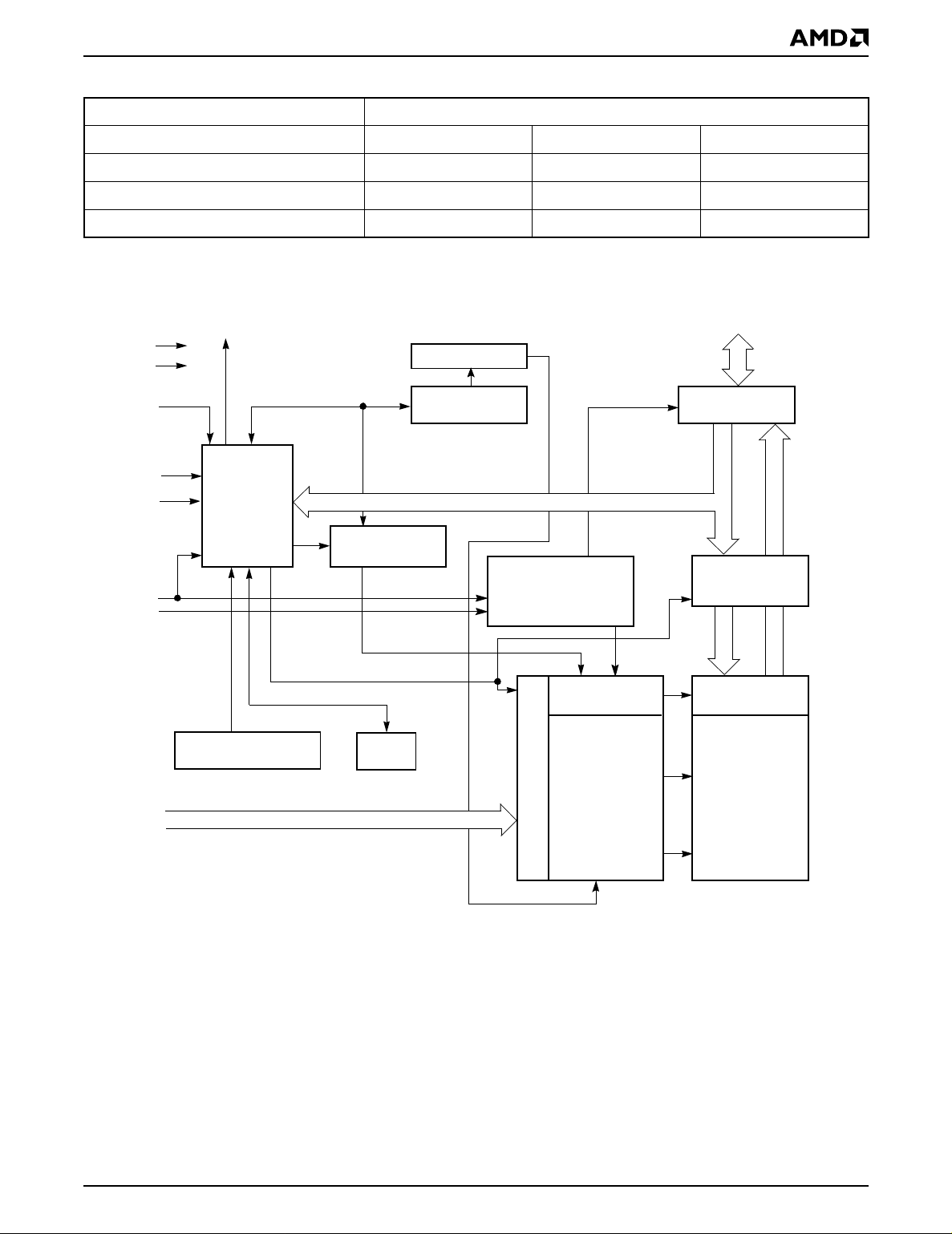
BLOCK DIAGRAM
DQ0
–
DQ15 (A-1)
Input/Output
Buffers
Data
Latch
V
CC
V
SS
RESET#
WE#
BYTE#
CE#
OE#
RY/BY#
State
Control
Command
Register
PGM Voltage
Generator
Sector Switches
Erase Voltage
Generator
Chip Enable
Output Enable
Logic
STB
A0–A18
VCC Detector
Timer
STB
Address Latch
Y-Decoder
X-Decoder
Y-Gating
Cell Matrix
22230A-1
Am29SL800C 3
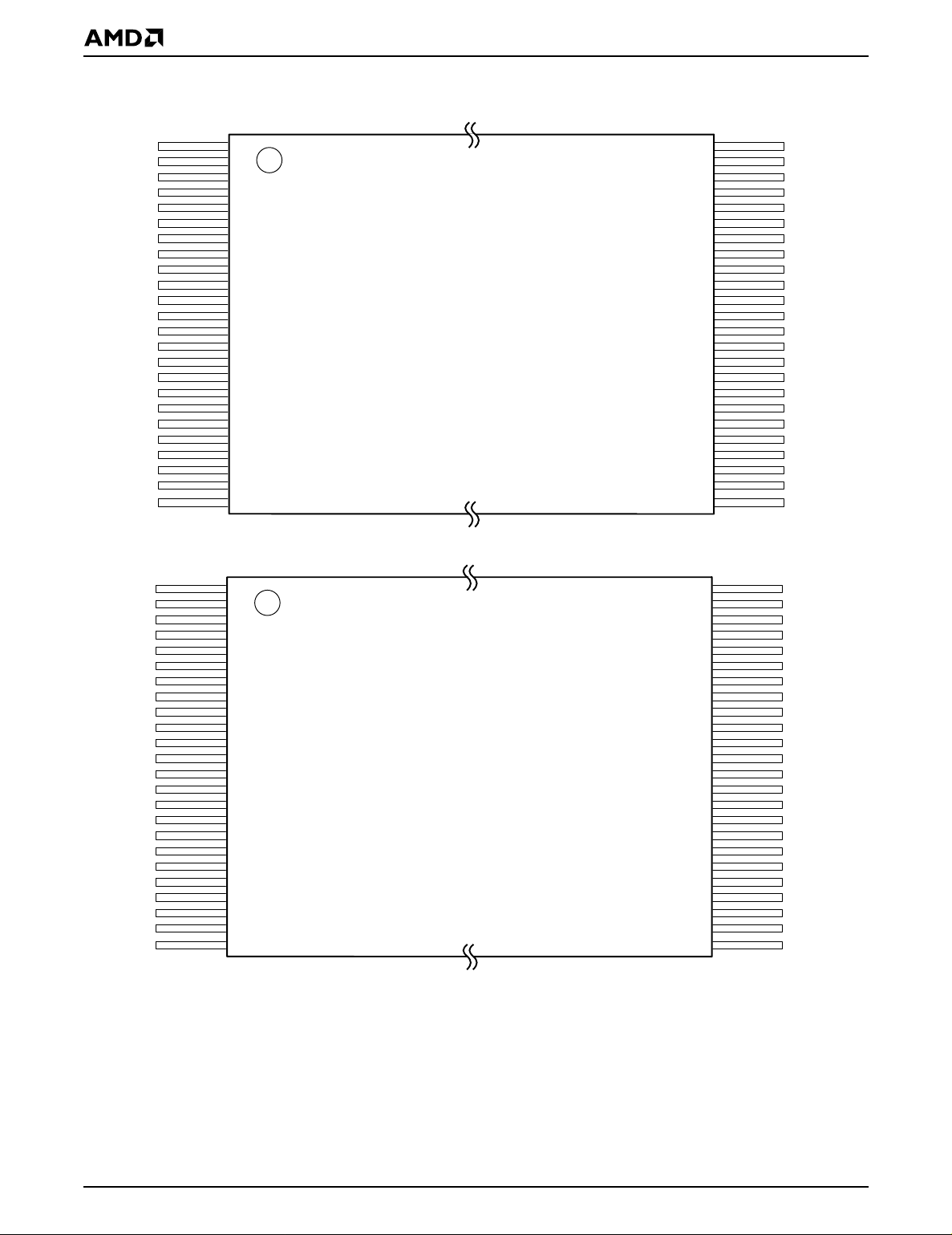
CONNECTION DIAGRAMS
PRELIMINARY
A15
A14
A13
A12
A11
A10
A9
A8
NC
NC
WE#
RESET#
NC
NC
RY/BY#
A18
A17
A7
A6
A5
A4
A3
A2
A1
A16
BYTE#
V
SS
DQ15/A-1
DQ7
DQ14
DQ6
DQ13
DQ5
DQ12
DQ4
V
CC
DQ11
DQ3
DQ10
DQ2
DQ9
DQ1
DQ8
DQ0
OE#
V
SS
CE#
A0
1
2
3
4
5
6
7
8
9
10
11
12
13
14
15
16
17
18
19
20
21
22
23
24
1
2
3
4
5
6
7
8
9
10
11
12
13
14
15
16
17
18
19
20
21
22
23
24
Standard TSOP
Reverse TSOP
48
47
46
45
44
43
42
41
40
39
38
37
36
35
34
33
32
31
30
29
28
27
26
25
48
47
46
45
44
43
42
41
40
39
38
37
36
35
34
33
32
31
30
29
28
27
26
25
A16
BYTE#
V
SS
DQ15/A-1
DQ7
DQ14
DQ6
DQ13
DQ5
DQ12
DQ4
V
CC
DQ11
DQ3
DQ10
DQ2
DQ9
DQ1
DQ8
DQ0
OE#
V
SS
CE#
A0
A15
A14
A13
A12
A11
A10
A9
A8
NC
NC
WE#
RESET#
NC
NC
RY/BY#
A18
A17
A7
A6
A5
A4
A3
A2
A1
4 Am29SL800C
22230A-2
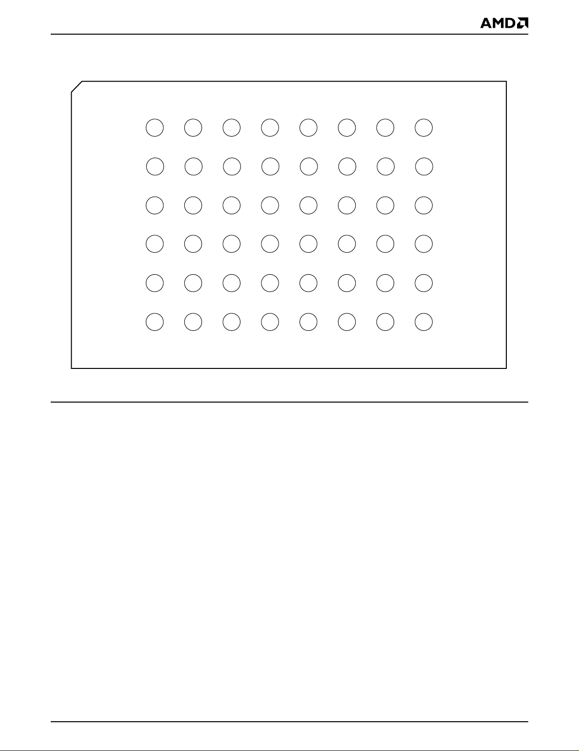
CONNECTION DIAGRAMS
A1 B1 C1 D1 E1 F1 G1 H1
PRELIMINARY
48-Ball FBGA (Bottom View)
A2 B2 C2 D2 E2 F2 G2 H2
A3 B3 C3 D3 E3 F3 G3 H3
A4 B4 C4 D4 E4 F4 G4 H4
A5 B5 C5 D5 E5 F5 G5 H5
A6 B6 C6 D6 E6 F6 G6 H6
Special Handling Instructions for FBGA Packages
Special handling is required for Flash Memory products
in FBGA packages.
CE#A0A1A2A4A3
BYTE#A16A15A14A12A13
OE# V
DQ9 DQ1DQ8DQ0A5A6A17A7
DQ11 DQ3DQ10DQ2NCA18NCRY/BY#
V
CC
DQ13 DQ6DQ14DQ7A11A10A8A9
DQ15/A-1 V
SS
DQ4DQ12DQ5NCNCRESET#WE#
SS
22230A-3
Flash memory devices in FBGA packages may be
damaged if exposed to ultrasonic cleaning methods.
The package and/or data integrity may be compromised
if the package body is exposed to temperatures above
150°C for prolonged periods of time.
Am29SL800C 5
PRELIMINARY
PIN CONFIGURATION
A0–A18 = 19 addresse s
DQ0–DQ14 = 15 data inputs/out pu ts
DQ15/A-1 = DQ15 (data input/output, word mode),
A-1 (LSB addre s s input, byte mode)
BYTE# = Selects 8-bit o r 16-bit mode
CE# = Chip enable
OE# = Output enable
WE# = Write en able
RESET# = Hardware reset pin, active low
RY/BY# = Ready/Busy# output
V
= 1.8–2.2 V single power supply
CC
V
SS
NC = Pin not connected internally
= Device ground
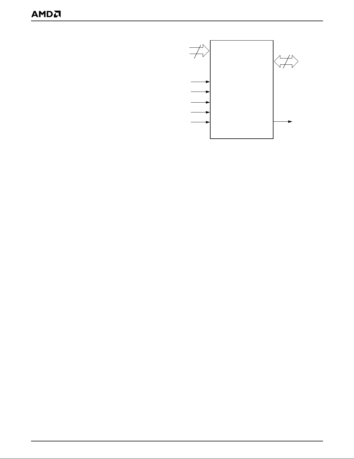
LOGIC SYMBOL
19
A0–A18
CE#
OE#
WE#
RESET#
BYTE# RY/BY#
16 or 8
DQ0–DQ15
(A-1)
22230A-4
6 Am29SL800C
PRELIMINARY
ORDERING INFORMATION
Standard Products
AMD stan dard produc ts ar e available in several pack ages an d opera ting ranges. Th e orde r numbe r (Valid Comb ination) is formed by a combination of the elements below.
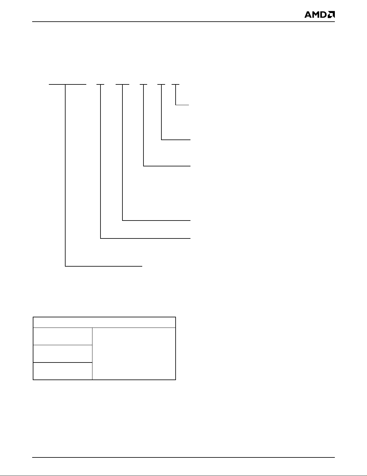
CE100Am29SL800C T
OPTIONAL PROCESSING
Blank = Standard Processing
B = Burn-in
(Contact an AMD representative for more information)
TEMPERATURE RANGE
C=Commercial (0°C to +70°C)
I = Industrial (–40°C to +85°C)
PACKAGE TYPE
E = 48-Pin Thin Small Outline Package (TSOP)
Standard Pinout (TS 048)
F = 48-Pin Thin Small Outline Package (TSOP)
Reverse Pinout (TSR048)
WB = 48-ball Fine-Pitch Ball Grid Array (FBGA)
0.80 mm pitch, 6 x 9 mm package
Am29SL800CT100,
Am29SL800CB100
Am29SL800CT120,
Am29SL800CB120
Am29SL800CT150,
Am29SL800CB150
Valid Combinations
EC, EI, FC, FI, WBC, WBI
SPEED OPTION
See Product Selector Guide and Valid Combinations
BOOT CODE SECTOR ARCHITECTURE
T = Top Sector
B = Bottom Sector
DEVICE NUMBER/DE SCRIP TION
Am29SL800C
8 Megabit (1 M x 8-Bit/512 K x 16-Bit) CMOS Flash Memory
1.8 Volt-only Read, Program, and Erase
Valid Combinations
Valid Combinations list configurations planned to be supported in volume for this device. Consult the local AMD sales
office to confirm availability of specific valid combinations and
to check on newly released combinations.
Am29SL800C 7

PRELIMINARY
DEVICE BUS OPERATIONS
This section describes the requirements and use of the
device bus operat ions, whi ch are init iated thro ugh the
internal command register. The command register itself does not occupy any addressable memory location. The register is composed of latches that store the
comman ds, along with the add ress an d data infor mation needed to execute the command. The contents of
Table 1. Am29SL800C Device Bus Operations
Operation CE# OE# WE# RESET#
Read L L H H A
Write L H L H A
V
±
Standby
Output Disable L H H H X High-Z High-Z High-Z
Reset X X X L X High-Z High-Z High-Z
Sector Protect (Note 2) L H L V
Sector Unprotect (Note 2) L H L V
Temporary Sector Unprotect X X X V
Legend:
L = Logic Low = V
Notes:
1. Addresses are A18:A0 in word mode (BYTE# = V
2. The sector protect and sector unprotect functions may also be implemented via programming equipment. See the “Sector
Protection/Unprotection” section.
, H = Logic High = VIH, VID = 10 ± 1.0 V, X = Don’t Care, AIN = Address In, DIN = Data In, D
IL
CC
0.3 V
XX
VCC ±
0.3 V
ID
ID
ID
), A18:A-1 in byte mode (BYTE# = VIL).
IH
the register serve as inputs to the internal state machine. The state machine outputs dictate the function of
the device. Table 1 lists th e d evice bus o pe ratio ns, th e
inputs and control lev els they require, and the resulting
output. The following s ubsections describe each of
these operations in further detail.
DQ8–DQ15
Addresses
(Note 1)
IN
IN
X High-Z High-Z High-Z
Sector Address,
A6 = L, A1 = H,
A0 = L
Sector Address,
A6 = H, A1 = H,
A0 = L
A
IN
DQ0–
DQ7
D
OUT
D
IN
D
IN
D
IN
D
IN
BYTE#
= V
IH
D
OUT
D
IN
XX
XX
D
IN
BYTE#
= V
IL
DQ8–DQ14 = High-Z,
DQ15 = A-1
High-Z
= Data Out
OUT
W ord/Byte Configuration
The BY TE# p in contr ol s whethe r the device data I/O pins
DQ15–DQ0 operate in the byte or word configuration. If the
BYTE# pin is set at logic ‘1’, the device is in word configuration, DQ 15–DQ0 are ac tive and con trolled by CE # and
OE#.
If the BYTE# pin is set at logic ‘0’, the device is in byte configuration, and only data I/O pins DQ0–DQ7 are active and
controlled by CE# and OE#. The data I/O pins DQ8–DQ14
are tri-stated, and the DQ15 pin is used as an input for the
LSB (A-1) address function.
Requirements for Reading Array Data
The internal state machine is set for reading array data
upon device power-up, or after a hardware reset. This ensures that no spurious alteration of the memory content occurs during the power transition. No co mmand is
necessary in this mode to obtain array data. Standard microproce ssor read cy cles tha t asse rt valid ad dresse s on
the device address inputs produce valid data on the device
data outputs. The device remains enabled for read access
until the command register contents are altered.
See “Reading Array Data” for m ore informati on. Refer to
the AC Read Operations table for timing specifications and
to Figure 13 for the timing diagram. I
teristics table represents the active current specification for
reading array data.
To read array data from the outputs, the system must driv e
the CE# and OE# pins to V
selects the device. OE# is the output control and gates
array data to the ou tput pins. W E# shoul d rem ain at V
The BYTE# pin determines whether the device outputs
array data in words or bytes.
. CE# is the power control and
IL
Writing Commands/Command Sequences
To write a command or command seque nce (whic h in-
.
IH
cludes programming data to the device and erasing sectors
of memory), the syste m must drive WE# and CE# to V
and OE# to V
8 Am29SL800C
in the DC Charac-
CC1
,
.
IH
IL

PRELIMINARY
For program operatio ns, the BYTE# pin deter mines
whether the dev ice accepts program data in bytes or
words. Refer to “Word/Byte Configuration” for more information.
The device features an Unlock Bypass mode to facilitate
faster programming. Once the device enters the Unlock
Bypass mode, only two write cycles are required to program a word or byte, instead of four. The “Word/Byte Program Command Sequence” section has details on
programming data to the device using bo th stand ard and
Unlock Bypass command sequences.
An erase operation can erase one sector, multiple sectors,
or the enti re device. Tables 2 and 3 indica te the add ress
space that eac h sector oc cup ie s. A “s ector addr ess ” co nsists of the address bits required to uniquely select a sector.
The “Command Definitions” section has details on erasing
a sector or the entire chip, or suspending/resuming the
erase operation.
After the system writes the autoselect command sequence, the device enters the autoselect mode. The system can then read autoselect codes from the internal
register (whic h is separate from the me mory array) on
DQ7–DQ0. Standard read cycle timings apply in this mode.
Refer to the Autoselect Mode and Autoselect Command
Sequence sections for more information.
I
in the DC Characteristics table repres ents the active
CC2
current speci fic ation fo r the w rite mode . T he “ AC Ch aracteristics” section contains timing specification tables and
timing diagrams for write operations.
Program and Erase Operation Status
During an erase or program operation, the system may
check the status of the operation by reading the status bits
on DQ7–DQ0. Standard read cycle timings and I
CC
read
specificat ions ap ply. Refer to “Write Opera tion Status” for
more information, and to “AC Characteristics” for timing diagrams.
Standby Mode
When the system is not reading or writing to the device, it
can plac e t he device in th e stan dby mo de. In th is m ode,
current consumption is greatly reduced, and the outputs
are placed in the high impedance state, independent of the
OE# input.
The device enters the CMOS standby mode when the CE#
and RESET# pins are both held at V
this is a more restricted voltage range than V
RESET# are held at V
, but not within V
IH
vice will be in the standby mode, but the standby current will
be greater. The device requires standard access time (t
for re ad ac ces s when th e devic e is i n ei ther of t hese
standby modes, before it is ready to read data.
The device also enters the standby mode when the RESET# pin is driven low. Ref er to the next section, RESET#:
Hardware Reset Pin.
± 0.3 V. (Note that
CC
.) If CE# and
IH
± 0.3 V, the de-
CC
CE
If the device is deselected during erasure or programming,
the de vice dra w s act ive cur r e nt unt i l the o p er a t io n is completed.
I
in the DC Characteristics table represents the standby
CC3
current specification.
Aut oma ti c S lee p Mod e
The automatic sleep mode minimizes Flash device energy
consumption. The device automatically enables this mode
when addresses remain stable for t
ACC
automatic sleep mode is independent of the CE#, WE#,
and OE# control signals. Standard address access timings
provide new data when addresses are changed. Whi le in
sleep mode, output data is latched and always a vailable to
the system. I
in the DC Characteristics table represents
CC4
the automatic sleep mode current specification.
RESET#: Hardware Rese t Pi n
The RESET# pin provides a hardware method of resetting
the device to reading array data. When the RESET# pin is
driven low for at l east a p er io d o f t
ately terminates any operation in progress, tristates all
output pins, and ignores all read/write commands for the
duration of the RESET# pulse. The device also resets the
internal state machine to reading array data. The operation
that was interrupted should be reinitiated once the device is
ready to accept another command sequence, to ensure
data integrity.
Current is reduced for the duration of the RESET# pulse.
When RESET# is held at V
CMOS standby current (I
not within V
±0.3 V, the standby current will be greater.
SS
SS
). If RESET# is held at VIL but
CC4
The RESET# pin may be tied to the system reset circuitry.
A system reset woul d thus also rese t the Fla sh memor y,
enabling the system to read the boot-up firmware from the
Flash m e mory.
If RESET# is asserted during a program or erase operation, the RY/BY# pin remains a “0” (busy) until the internal
reset operation is complete, which requires a time of
t
(during Embedded Algorithms). The system can
READY
thus monitor RY/BY# to determine whether the reset operation is complete. If RESET# is asserted when a program
or erase operation is not executing (RY/BY# pin is “1”), the
reset operation is completed within a time of t
during Embedded Algorithms). The system can read data
t
after the RESET# pin returns to VIH.
RH
Refer to the AC Characteristics tables for RESET# parameters and to Figure 14 for the timing diagram.
Output Disable Mode
)
When the OE# input is at VIH, output from the device is disabled. The out put pi ns are plac ed in the high impedan ce
state.
, the device immedi-
RP
±0.3 V, the device draws
+ 50 ns. The
(not
READY
Am29SL800C 9

PRELIMINARY
Table 2. Am29SL800CT Top Boot Block Sector Address Table
Sector Size
(Kbytes/
Sector A18 A17 A16 A15 A14 A13 A12
SA00000XXX 64/32 00000h–0FFFFh 00000h–07FFFh
SA10001XXX 64/32 10000h–1FFFFh 08000h–0FFFFh
SA20010XXX 64/32 20000h–2FFFFh 10000h–17FFFh
SA30011XXX 64/32 30000h–3FFFFh 18000h–1FFFFh
SA40100XXX 64/32 40000h–4FFFFh 20000h–27FFFh
SA50101XXX 64/32 50000h–5FFFFh 28000h–2FFFFh
SA60110XXX 64/32 60000h–6FFFFh 30000h–37FFFh
SA70111XXX 64/32 70000h–7FFFFh 38000h–3FFFFh
SA81000XXX 64/32 80000h–8FFFFh 40000h–47FFFh
SA91001XXX 64/32 90000h–9FFFFh 48000h–4FFFFh
SA10 1010XXX 64/32 A0000h–AFFFFh 50000h–57FFFh
SA11 1011XXX 64/32 B0000h–BFFFFh 58000h–5FFFFh
SA12 1100XXX 64/32C0000h–CFFFFh 60000h–67FFFh
SA13 1101XXX 64/32D0000h–DFFFFh 68000h–6FFFFh
Kwords)
Address Range (in hexadecimal)
(x8)
Address Range
(x16)
Address Range
SA14 1110XXX 64/32 E0000h–EFFFFh 70000h–77FFFh
SA15 11110XX 32/16 F0000h–F7FFFh 78000h–7BFFFh
SA16 1111100 8/4 F8000h–F9FFFh 7C000h–7CFFFh
SA17 1111101 8/4 FA000h–FBFFFh 7D000h–7DFFFh
SA18 111111X 16/8 FC000h–FFFFFh 7E000h–7FFFFh
10 Am29SL800C

PRELIMINARY
Table 3. Am29SL800CB Bottom Boot Block Sector Address Table
Sector Size
(Kbytes/
Sector A18 A17 A16 A15 A14 A13 A12
SA0000000X 16/8 00000h–03FFFh 00000h–01FFFh
SA10000010 8/4 04000h–05FFFh 02000h–02FFFh
SA20000011 8/4 06000h–07FFFh 03000h–03FFFh
SA300001XX 32/16 08000h–0FFFFh 04000h–07FFFh
SA40001XXX 64/32 10000h–1FFFFh 08000h–0FFFFh
SA50010XXX 64/32 20000h–2FFFFh 10000h–17FFFh
SA60011XXX 64/32 30000h–3FFFFh 18000h–1FFFFh
SA70100XXX 64/32 40000h–4FFFFh 20000h–27FFFh
SA80101XXX 64/32 50000h–5FFFFh 28000h–2FFFFh
SA90110XXX 64/32 60000h–6FFFFh 30000h–37FFFh
SA10 0111XXX 64/32 70000h–7FFFFh 38000h–3FFFFh
SA11 1000XXX 64/32 80000h–8FFFFh 40000h–47FFFh
Kwords)
Address Range (in hexadecimal)
(x8)
Address Range
(x16)
Address Range
SA12 1001XXX 64/32 90000h–9FFFFh 48000h–4FFFFh
SA13 1010XXX 64/32 A0000h–AFFFFh 50000h–57FFFh
SA14 1011XXX 64/32 B0000h–BFFFFh 58000h–5FFFFh
SA15 1100XXX 64/32C0000h–CFFFFh 60000h–67FFFh
SA16 1101XXX 64/32D0000h–DFFFFh 68000h–6FFFFh
SA17 1110XXX 64/32 E0000h–EFFFFh 70000h–77FFFh
SA18 1111XXX 64/32 F0000h–FFFFFh 78000h–7FFFFh
Note for Tables 2 and 3: Address range is A18:A-1 in byte mode and A18:A0 in word mode. See “Word/Byte Configuration”
section for more information.
Am29SL800C 11

PRELIMINARY
Autoselect Mode
The autoselect mode provides manufacturer and device identification, and sector protection verification,
through identifier codes output on DQ7–DQ0. This
mode is primarily intended for programming equipment
to automatically match a device to be programmed with
its correspo nding programmi ng algorithm . However,
the aut osel ect co des can also be a cces sed in -sy stem
through the command register.
When using programming equipment, the autoselect
mode requires V
A1, and A 0 must be a s shown i n Table 4. In addi tion,
Description Mode CE# OE# WE#
Manufacturer ID: AMD L L H X X V
Device ID:
Am29SL800C
(Top Boot Block)
on address pin A9. Address pins A6,
ID
Table 4. Am29SL800C Autoselect Codes (High Voltage Method)
A11
A18
to
to
A10 A9
A12
Word L L H
Byte L L H X EAh
XXV
when verifying sector protection, the sector address
must appear on the app ropri ate highest or der addres s
bits (see Tables 2 and 3). Table 4 shows the remaining
address bits that are don’t care. When all necessary bits
have been set as required, the programming equipment
may then read the corresp onding identifier cod e on
DQ7–DQ0.
To access the autoselect codes in-system, the host
system can issue the autoselect command via the
comma nd reg ister, as s hown in Table 5. T his meth od
does not require V
. See “Command Definitions” for
ID
details on using the autoselect mode.
A8
to
A7 A6
XLXLL X 01h
ID
XLXLH
ID
A5
to
A2 A1 A0
DQ8
to
DQ15
22h EAh
DQ7
to
DQ0
Device ID:
Am29SL800C
(Bottom Boot Block)
Sector Protection V erification L L H SA X V
L = Logic Low = VIL, H = Logic High = VIH, SA = Sector Address, X = Don’t care.
Sector Protection/Unprotection
The h ardwar e sect or p rotec tion fe ature disabl es bot h
program and erase operations in any sector. The hardware sect or unp rotecti on feature r e-enables both p rogram and erase operations in previously protected
sectors. Sector protection/unprotection can be implemente d via two method s.
The primary method requires V
only, and can be implemented either in-system or via
Word L L H
Byte L L H X 6Bh
XXV
XLXLH
ID
XLXHL
ID
an AMD represe ntative to request the doc ument containing further details.
The device i s shipped wit h all sector s unprotected .
AMD offers the option of program ming and protectin g
sectors at its factory prior to shipping the device
through AMD’s ExpressFlash™ Service. Contact an
AMD representative for details.
on the RESET# pin
ID
It is possible to determine whether a sector is protected
or unprotected. See “Autoselect Mode” for detail s.
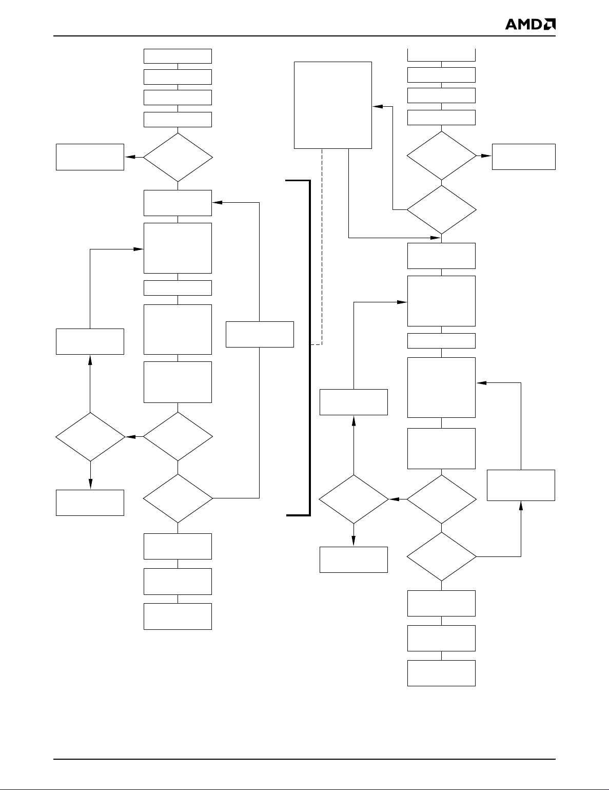
programming equipment. Figure 1 shows the algorithm s and Fig ure 23 shows the ti ming diagram . Thi s
method uses standard microprocessor bus cycle timing. For sector unprotect, all unprotected sectors must
first be protected prior to the first sector unprotect write
cycle.
The alternate method intended only for programming
equipment requires V
on address pin A9 and OE#.
ID
This method is compatible with programmer routines
writte n for ea rli er 3 . 0 v o l t- o nly AMD fl a sh d evice s . Pu blication number 21622 contains further details. Contact
Temporary Sector Unprotect
This feature allows temporary unprotection of previously protected sectors to change data in-system. The
Sector U n pr ot ect m ode i s activated by s ett ing th e RESET# pi n to V
sectors can be programmed or erased by selecting the
sector ad dresses. Once V
SET# pin, all the previously protected sectors are
protected a gain. Figure 2 sh ows the algorithm, a nd
Figure 22 shows the timing diagrams, for this feature.
22h 6Bh
X
X
. During thi s mode, for me rly pr otecte d
ID
is rem oved from th e RE-
ID
01h
(protected)
00h
(unprotected)
12 Am29SL800C
PRELIMINARY
Temporary Sector
Unprotect Mode
Increment
PLSCNT
No
PLSCNT
= 25?
Yes
Device failed
Sector Protect
Algorithm
START
PLSCNT = 1
RESET# = V
Wait 1 µs
No
First Write
Cycle = 60h?
Set up sector
address
Sector Protect:
Write 60h to sector
address with
A6 = 0, A1 = 1,
A0 = 0
Wait 150 µs
Verify Sector
Protect: Write 40h
to sector address
with A6 = 0,
A1 = 1, A0 = 0
Read from
sector address
with A6 = 0,
A1 = 1, A0 = 0
No
Data = 01h?
Protect another
sector?
Remove V
from RESET#
Write reset
command
Sector Protect
complete
Yes
Yes
No
START
Protect all sectors:
The indicated portion
of the sector protect
ID
Reset
PLSCNT = 1
Yes
ID
algorithm must be
performed for all
unprotected sectors
prior to issuing the
first sector
unprotect address
Increment
PLSCNT
No
PLSCNT
= 1000?
Yes
Device failed
Sector Unprotect
PLSCNT = 1
RESET# = V
Wait 1 µs
First Write
Cycle = 60h?
No
All sectors
protected?
Set up first sector
address
Sector Unprotect:
Write 60h to sector
address with
A6 = 1, A1 = 1,
A0 = 0
Wait 15 ms
Verify Sector
Unprotect: Write
40h to sector
address with
A6 = 1, A1 = 1,
A0 = 0
Read from
sector address
with A6 = 1,
A1 = 1, A0 = 0
No
Data = 00h?
Last sector
verified?
Remove V
from RESET#
Yes
Yes
Yes
Yes
ID
No
Temporary Sector
Unprotect Mode
Set up
next sector
address
No
ID
Algorithm
Write reset
command
Sector Unprotect
complete
Figure 1. In-System Sector Protect/Unprotect Algorithms
Am29SL800C 13
22230A-5
 Loading...