

Page 1

Am29LV800D
Data Sheet
For new designs, S29AL008D supersedes Am29LV800D and is the factory-recommended migration
path. Please refer to the S29AL008D Data Sheet for specifications and ordering information.
July 2003
The following document specifies Spansion memory products that are now offered by both Advanced
Micro Devices and Fujitsu. Although the document is marked with the name of the company that originally developed the specification, these products will be offered to customers of both AMD and
Fujitsu.
Continuity of Specifications
There is no change to this datasheet as a result of offering the device as a Spansion product. Any
changes that have been made are the result of normal datasheet improvement and are noted in the
document revision summary, where supported. Future routine revisions will occur when appropriate,
and changes will be noted in a revision summary.
Continuity of Ordering Part Numbers
AMD and Fujitsu continue to support existing part numbers beginning with “Am” and “MBM”. To order
these products, please use only the Ordering Part Numbers listed in this document.
For More Information
Please contact your local AMD or Fujitsu sales office for additional information about Spansion
memory solutions.
Publication Number Am29LV800D_00 Revision A Amendment 4 Issue Date January 21, 2005
Page 2

THIS PAGE LEFT INTENTIONALLY BLANK.
Page 3

PRELIMINARY
Am29LV800D
8 Megabit (1 M x 8-Bit/512 K x 16-Bit)
CMOS 3.0 Volt-only Boot Sector Flash Memory
For new designs, S29AL008D supersedes Am29LV800D and is the factory-recommended migration
path. Please refer to the S29AL008D Data Sheet for specifications and ordering information.
Distinctive Characteristics
■ Single power supply operation
— 2.7 to 3.6 volt read and write operations
for battery-powered applications
■ Manufactured on 0.23 µm process
technology
— Compatible with 0.32 µm Am29LV800
device
■ High performance
— Access times as fast as 70 ns
■ Ultra low power consumption (typical
values at 5
— 200 nA Automatic Sleep mode current
— 200 nA standby mode current
— 7 mA read current
— 15 mA program/erase current
■ Flexible sector architecture
— One 16 Kbyte, two 8 Kbyte, one 32 Kbyte, and
fifteen 64 Kbyte sectors (byte mode)
— One 8 Kword, two 4 Kword, one 16 Kword, and
fifteen 32 Kword sectors (word mode)
— Supports full chip erase
— Sector Protection features:
A hardware method of locking a sector to prevent
any program or erase operations within that
sector
Sectors can be locked in-system or via
programming equipment
Temporary Sector Unprotect feature allows code
changes in previously locked sectors
■ Unlock Bypass Program Command
— Reduces overall programming time when
issuing multiple program command
sequences
MHz)
■ Top or bottom boot block configurations
available
■ Embedded Algorithms
— Embedded Erase algorithm automatically
preprograms and erases the entire chip or any
combination of designated sectors
— Embedded Program algorithm
automatically writes and verifies data at
specified addresses
■ Minimum 1 million write cycle guarantee
per sector
■ 20-year data retention at 125°C
— Reliable operation for the life of the system
■ Package option
— 48-ball FBGA
— 48-pin TSOP
—44-pin SO
■ Compatibility with JEDEC standards
— Pinout and software compatible with single-
power supply Flash
— Superior inadvertent write protection
■ Data# Polling and toggle bits
— Provides a software method of detecting
program or erase operation completion
■ Ready/Busy# pin (RY/BY#)
— Provides a hardware method of detecting
program or erase cycle completion
■ Erase Suspend/Erase Resume
— Suspends an erase operation to read data from,
or program data to, a sector that is not being
erased, then resumes the erase operation
■ Hardware reset pin (RESET#)
— Hardware method to reset the device to
reading array data
This document contains information on a product under development at FASL LLC. The information is intended to
help you evaluate this product. FASL LLC reserves the right to change or discontinue work on this proposed produc t
without notice.
Publication Am29LV800D_00 Rev. A Amend. 4
Issue Date: January 21, 2005
Page 4

General Description
PRELIMINARY
The Am29LV800D is an 8 Mbit, 3.0 volt-only
Flash memory organized as 1,048,576 bytes or
524,288 words. The device is offered in 48-ball
FBGA, 44-pin SO, and 48-pin TSOP packages.
For more information, refer to publication
number 21536. The word-wide data (x16)
appears on DQ15–DQ0; the byte-wide (x8) data
appears on DQ7–DQ0. This device requires only
a single, 3.0 volt VCC supply to perform read,
program, and erase operations. A standard
EPROM programmer can also be used to program
and erase the device.
This device is manufactured using AMD’s 0.23
µm process technology, and offers all the fea
tures and benefits of the Am29LV800B, which
was manufactured using 0.32 µm process technology.
The standard device offers access times of 70,
90, and 120 ns, allowing high speed micropro
cessors to operate without wait states. To eliminate bus contention the device has separate
chip enable (CE#), write enable (WE#) and
output enable (OE#) controls.
The device requires only a single 3.0 volt
power supply for both read and write func
tions. Internally generated and regulated voltages are provided for the program and erase
operations.
The device is entirely command set compatible
with the JEDEC single-power-supply Flash
standard. Commands are written to the
command register using standard microprocessor write timings. Register contents serve as
input to an internal state-machine that controls
the erase and programming circuitry. Write
cycles also internally latch addresses and data
needed for the programming and erase opera
tions. Reading data out of the device is similar
to reading from other Flash or EPROM devices.
Device programming occurs by executing the
program command sequence. This initiates the
Embedded Program algorithm—an internal
algorithm that automatically times the program
pulse widths and verifies proper cell margin. The
Unlock Bypass mode facilitates faster programming times by requiring only two write
cycles to program data instead of four.
Device erasure occurs by executing the erase
command sequence. This initiates the
Embedded Erase algorithm—an internal algorithm that automatically preprograms the array
(if it is not already programmed) before exe
-
-
-
-
-
cuting the erase operation. During erase, the
device automatically times the erase pulse
widths and verifies proper cell margin.
The host system can detect whether a program
or erase operation is complete by observing the
RY/BY# pin, or by reading the DQ7 (Data#
Polling) and DQ6 (toggle) status bits. After a
program or erase cycle has been completed, the
device is ready to read array data or accept
another command.
The sector erase architecture allows memory
sectors to be erased and reprogrammed without
affecting the data contents of other sectors. The
device is fully erased when shipped from the
factory.
Hardware data protection measures include
a low V
write operations during power transitions. The
hardware sector protection feature disables
both program and erase operations in any combination of the sectors of memory. This can be
achieved in-system or via programming equip
ment.
The Erase Suspend feature enables the user to
put erase on hold for any period of time to read
data from, or program data to, any sector that
is not selected for erasure. True background
erase can thus be achieved.
The hardware RESET# pin terminates any
operation in progress and resets the internal
state machine to reading array data. The
RESET# pin may be tied to the system reset circuitry. A system reset would thus also reset the
device, enabling the system microprocessor to
read the boot-up firmware from the Flash
memory.
The device offers two power-saving features.
When addresses have been stable for a specified
amount of time, the device enters the auto-
matic sleep mode. The system can also place
the device into the standby mode. Power consumption is greatly reduced in both these
modes.
AMD’s Flash technology combines years of Flash
memory manufacturing experience to produce
the highest levels of quality, reliability and cost
effectiveness. The device electrically erases
all bits within a sector simultaneously via
Fowler-Nordheim tunneling. The data is programmed using hot electron injection.
detector that automatically inhibits
CC
-
2Am29LV800DAm29LV800D_00_A4_E January 21, 2005
Page 5

PRELIMINARY
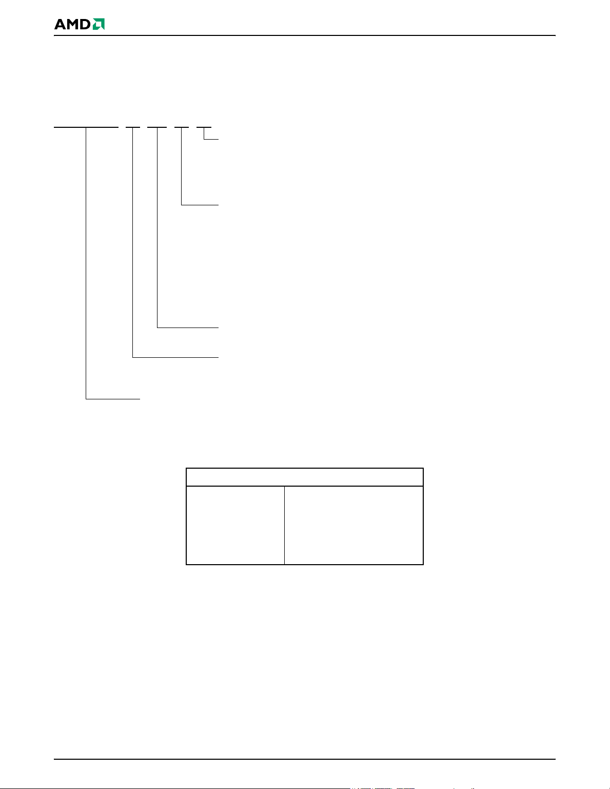
Table Of Contents
Product Selector Guide . . . . . . . . . . . . . . . . . . . . . 4
Block Diagram . . . . . . . . . . . . . . . . . . . . . . . . . . . . . 4
Connection Diagrams . . . . . . . . . . . . . . . . . . . . . . 5
Special Handling Instructions for FBGA Package .............. 7
Pin Configuration. . . . . . . . . . . . . . . . . . . . . . . . . . 7
Logic Symbol . . . . . . . . . . . . . . . . . . . . . . . . . . . . 7
Ordering Information . . . . . . . . . . . . . . . . . . . . . . . 8
Standard Products ......................................................................8
Valid Combinations . . . . . . . . . . . . . . . . . . . . . . . . . 9
Device Bus Operations . . . . . . . . . . . . . . . . . . . . . .10
Table 1. Am29LV800D Device Bus Operations .10
Word/Byte Configuration ...................................................... 10
Requirements for Reading Array Data ............................... 10
Writing Commands/Command Sequences .........................11
Program and Erase Operation Status ...................................11
Standby Mode ..............................................................................11
Automatic Sleep Mode ..............................................................11
RESET#: Hardware Reset Pin .................................................11
Output Disable Mode ...............................................................12
Table 2. Am29LV800DT Top Boot Block
Sector Addresses ........................................12
Table 3. Am29LV800DB Bottom Boot Block
Sector Addresses ........................................13
Autoselect Mode ........................................................................13
Table 4. Am29LV800D Autoselect Codes
(High Voltage Method) ................................14
Sector Protection/Unprotection .......................................... 14
Temporary Sector Unprotect ............................................... 14
Figure 1. Temporary Sector Unprotect
Operation .................................................. 15
Figure 2. In-System Sector Protect/
Sector Unprotect Algorithms ........................ 16
Hardware Data Protection .....................................................17
Command Definitions . . . . . . . . . . . . . . . . . . . . . . 17
Reading Array Data ...................................................................17
Reset Command .........................................................................17
Autoselect Command Sequence .......................................... 18
Word/Byte Program Command Sequence .......................18
Figure 1. Program Operation ........................ 19
Chip Erase Command Sequence .......................................... 19
Sector Erase Command Sequence ...................................... 19
Erase Suspend/Erase Resume Commands ....................... 20
Figure 1. Erase Operation ............................ 21
Table 5. Am29LV800D Command Definitions ..21
Write Operation Status . . . . . . . . . . . . . . . . . . . . 22
DQ7: Data# Polling ..................................................................22
Figure 1. Data# Polling Algorithm ................. 23
RY/BY#: Ready/Busy# .............................................................23
DQ6: Toggle Bit I ......................................................................24
DQ2: Toggle Bit II .....................................................................24
Reading Toggle Bits DQ6/DQ2 ............................................24
DQ5: Exceeded Timing Limits ..............................................25
DQ3: Sector Erase Timer .......................................................25
Figure 1. Toggle Bit Algorithm ...................... 25
Table 6. Write Operation Status ....................26
Absolute Maximum Ratings . . . . . . . . . . . . . . . . 27
Operating Ranges. . . . . . . . . . . . . . . . . . . . . . . . . 27
DC Characteristics . . . . . . . . . . . . . . . . . . . . . . . . .28
CMOS Compatible .................................................................. 28
Figure 1. I
and Automatic Sleep Currents) .................... 29
Figure 1. Typical I
Current vs. Time (Showing Active
CC1
vs. Frequency ............. 29
CC1
Test Conditions . . . . . . . . . . . . . . . . . . . . . . . . . . .30
Figure 1. Test Setup................................... 30
Table 7. Test Specifications ........................................30
Key to Switching Waveforms. . . . . . . . . . . . . . . . 30
Figure 1. Input Waveforms and
Measurement Levels................................... 30
AC Characteristics . . . . . . . . . . . . . . . . . . . . . . . . . 31
Read Operations ........................................................................31
Figure 1. Read Operations Timings ............... 31
Hardware Reset (RESET#) ....................................................32
Figure 1. RESET# Timings........................... 32
Word/Byte Configuration (BYTE#) ..................................33
Figure 1. BYTE# Timings for Read
Operations ................................................ 34
Figure 1. BYTE# Timings for Write
Operations ................................................ 34
Erase/Program Operations ....................................................35
Figure 1. Program Operation Timings............ 36
Figure 1. Chip/Sector Erase Operation
Timings .................................................... 37
Figure 1. Data# Polling Timings (During
Embedded Algorithms) ............................... 38
Figure 1. Toggle Bit Timings (During
Embedded Algorithms) ............................... 38
Figure 1. DQ2 vs. DQ6 ............................... 39
Temporary Sector Unprotect ...............................................39
Figure 1. Temporary Sector Unprotect
Timing Diagram ......................................... 39
Figure 1. Sector Protect/Unprotect
Timing Diagram ......................................... 40
Alternate CE# Controlled
Erase/Program Operations .................................................... 41
Figure 1. Alternate CE# Controlled Write
Operation Timings...................................... 42
Erase and Programming Performance . . . . . . . . .43
Latchup Characteristics . . . . . . . . . . . . . . . . . . . . 43
TSOP and SO Pin Capacitance . . . . . . . . . . . . . . 43
Data Retention . . . . . . . . . . . . . . . . . . . . . . . . . . . 43
Physical Dimensions* . . . . . . . . . . . . . . . . . . . . . . .44
TS 048—48-Pin Standard TSOP ........................................ 44
TSR048—48-Pin Reverse TSOP .........................................45
FBB 048—48-Ball Fine-Pitch Ball Grid Array
(FBGA) 6 x 9 mm ................................................................... 46
Physical Dimensions . . . . . . . . . . . . . . . . . . . . . . . 47
VBK 048 - 48 Ball Fine-Pitch Ball Grid Array
(FBGA) 6.15 x 8.15 mm .............................................................47
SO 044—44-Pin Small Outline Package ..........................48
Revision Summary . . . . . . . . . . . . . . . . . . . . . . . . .49
January 21, 2005 Am29LV800D_00_A4_E Am29LV800D 3
Page 6
PRELIMINARY
Product Selector Guide
Family Part Number Am29LV800D
Speed Options Full Voltage Range: VCC = 2.7–3.6 V -70 -90 -120
Max access time, ns (t
Max CE# access time, ns (tCE) 70 90 120
Max OE# access time, ns (tOE) 30 35 50
Note: See “AC Characteristics” for full specifications.
) 70 90 120
ACC
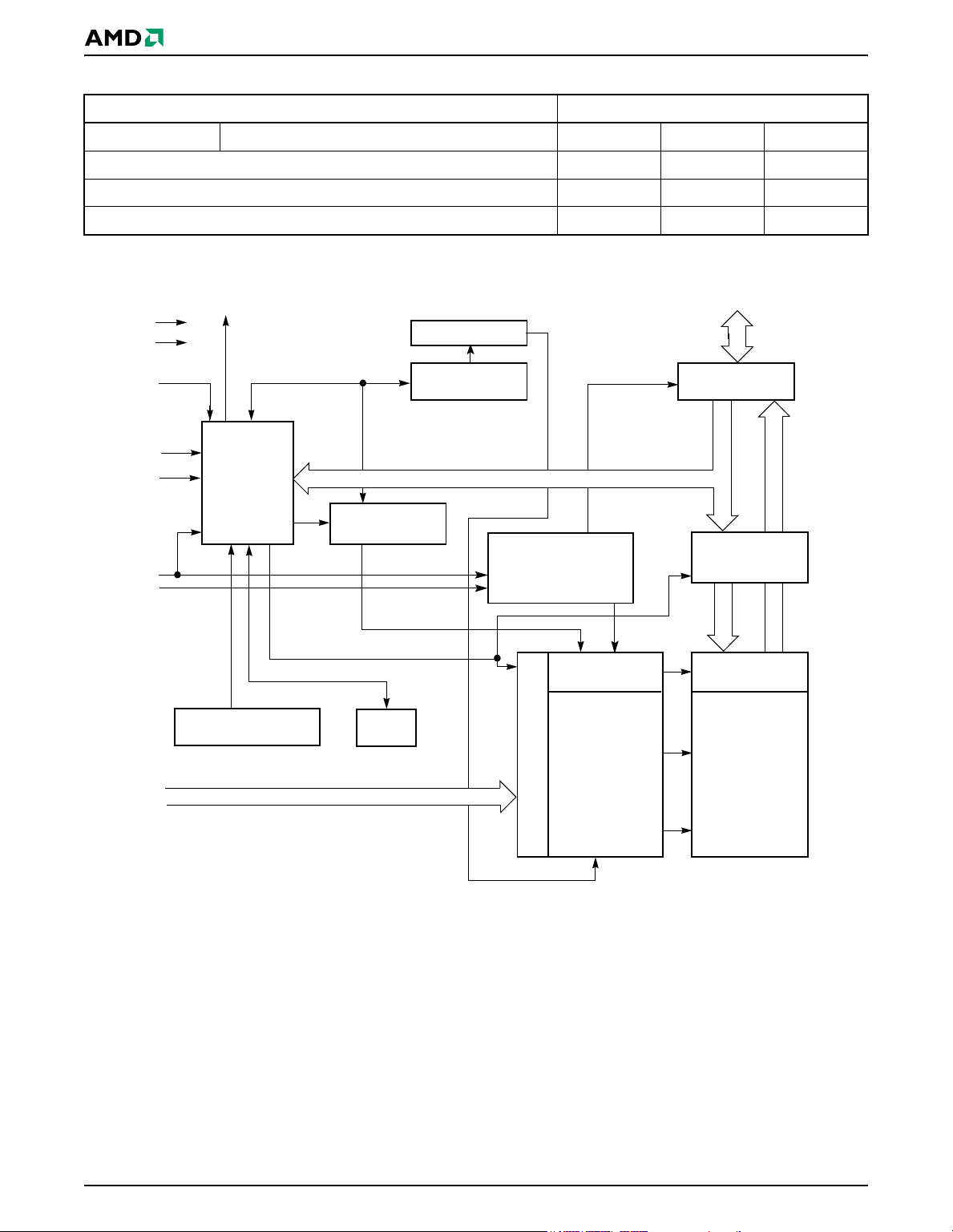
Block Diagram
DQ0–DQ15 (A-1)
Input/Output
Buffers
Data
STB
V
CC
V
SS
RESET#
WE#
BYTE#
CE#
OE#
RY/BY#
State
Control
Command
Register
Sector Switches
Erase Voltage
Generator
PGM Voltage
Generator
Chip Enable
Output Enable
A0–
VCC Detector
Timer
STB
Address Latch
Y-Decoder
X-Decoder
Y-Gating
Cell Matrix
4Am29LV800DAm29LV800D_00_A4_E January 21, 2005
Page 7
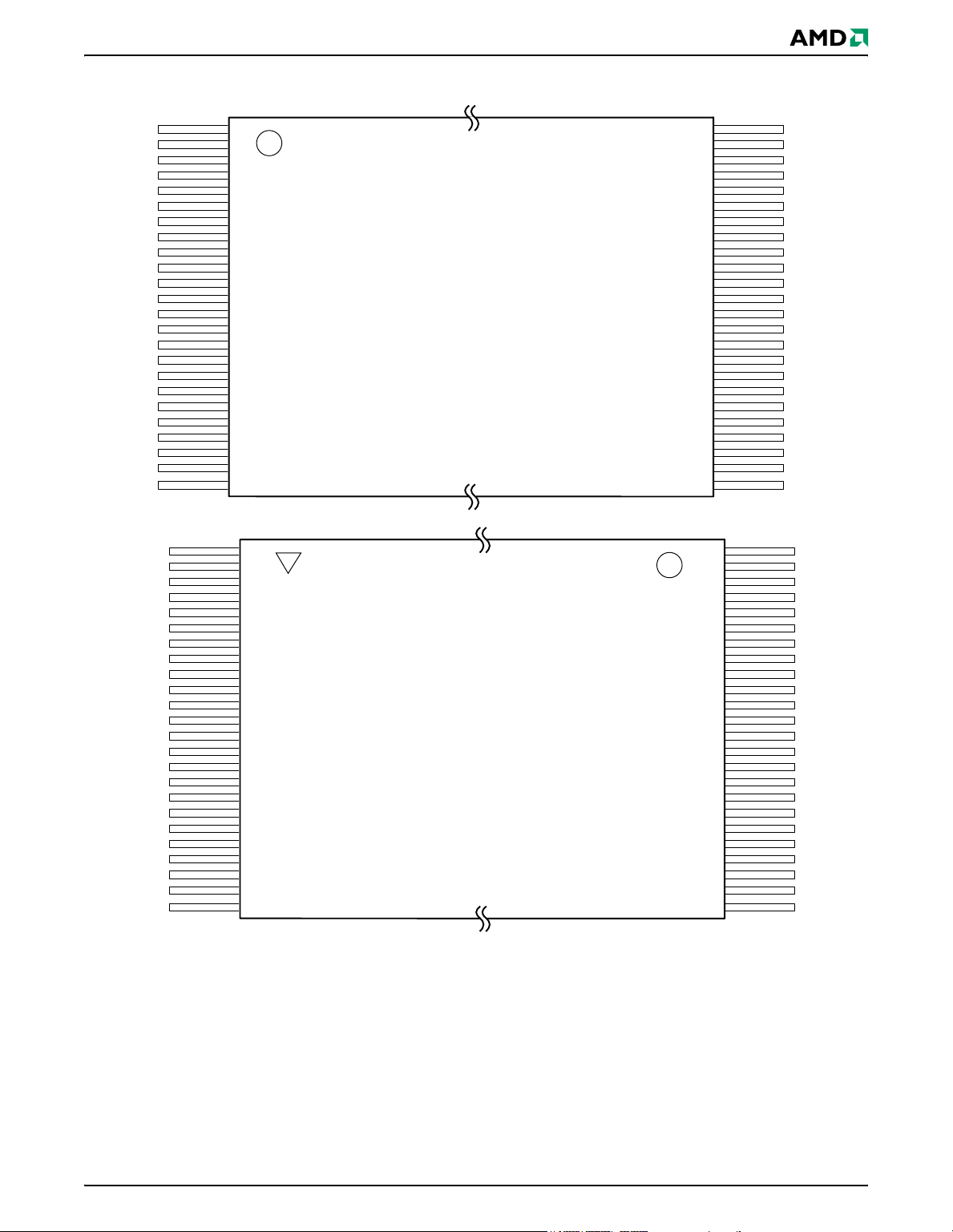
Connection Diagrams
PRELIMINARY
A15
A14
A13
A12
A11
A10
A9
A8
NC
NC
WE#
RESET#
NC
NC
RY/BY#
A18
A17
A7
A6
A5
A4
A3
A2
A1
A16
BYTE#
V
DQ15/A-1
DQ7
DQ14
DQ6
DQ13
DQ5
DQ12
DQ4
V
DQ11
DQ3
DQ10
DQ2
DQ9
DQ1
DQ8
DQ0
OE#
V
CE#
SS
CC
SS
A0
1
2
3
4
5
6
7
8
9
10
11
12
13
14
15
16
17
18
19
20
21
22
23
24
1
2
3
4
5
6
7
8
9
10
11
12
13
14
15
16
17
18
19
20
21
22
23
24
Standard TSOP
Reverse TSOP
48
47
46
45
44
43
42
41
40
39
38
37
36
35
34
33
32
31
30
29
28
27
26
25
48
47
46
45
44
43
42
41
40
39
38
37
36
35
34
33
32
31
30
29
28
27
26
25
A16
BYTE#
V
SS
DQ15/A-1
DQ7
DQ14
DQ6
DQ13
DQ5
DQ12
DQ4
V
CC
DQ11
DQ3
DQ10
DQ2
DQ9
DQ1
DQ8
DQ0
OE#
V
SS
CE#
A0
A15
A14
A13
A12
A11
A10
A9
A8
NC
NC
WE#
RESET#
NC
NC
RY/BY#
A18
A17
A7
A6
A5
A4
A3
A2
A1
Am29LV800D_
January 21, 2005 Am29LV800D_00_A4_E Am29LV800D 5
Page 8
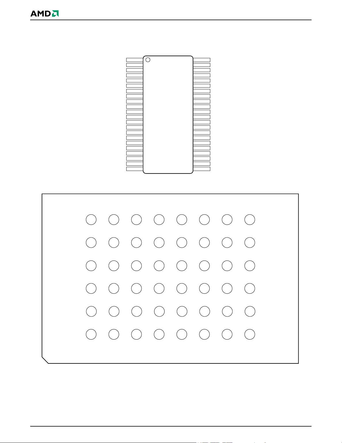
Connection Diagrams
PRELIMINARY
RY/BY#
A18
A17
A7
A6
A5
A4
A3
A2
A1
A0
CE#
V
OE#
DQ0
DQ8
DQ1
DQ9
DQ2
DQ10
DQ3
DQ11
1
2
3
4
5
6
7
8
9
SO
10
11
12
13
SS
14
15
16
17
18
19
20
21
22
44
43
42
41
40
39
38
37
36
35
34
33
32
31
30
29
28
27
26
25
24
23
RESET#
WE#
A8
A9
A10
A11
A12
A13
A14
A15
A16
BYTE#
V
SS
DQ15/A-1
DQ7
DQ14
DQ6
DQ13
DQ5
DQ12
DQ4
V
CC
FBGA
Top View, Balls Facing Down
A6 B6 C6 D6 E6 F6 G6 H6
BYTE#A16A15A14A12A13
DQ15/A-1 V
SS
A5 B5 C5 D5 E5 F5 G5 H5
DQ13 DQ6DQ14DQ7A11A10A8A9
A4 B4 C4 D4 E4 F4 G4 H4
V
CC
DQ4DQ12DQ5NCNCRESET#WE#
A3 B3 C3 D3 E3 F3 G3 H3
DQ11 DQ3DQ10DQ2NCA18NCRY/BY#
A2 B2 C2 D2 E2 F2 G2 H2
DQ9 DQ1DQ8DQ0A5A6A17A7
A1 B1 C1 D1 E1 F1 G1 H1
CE#A0A1A2A4A3
OE# V
SS
6Am29LV800DAm29LV800D_00_A4_E January 21, 2005
Page 9
PRELIMINARY
Special Handling Instructions for FBGA Package
Special handling is required for Flash Memory
products in FBGA packages.
Flash memory devices in FBGA packages may
be damaged if exposed to ultrasonic cleaning
methods. The package and/or data integrity
may be compromised if the package body is
exposed to temperatures above 150°C for prolonged periods of time.
Pin Configuration
A0–A18 = 19 addresses
DQ0–DQ14= 15 data inputs/outputs
DQ15/A-1 = DQ15 (data input/output, word
mode),
A-1 (LSB address input, byte
mode)
BYTE# = Selects 8-bit or 16-bit mode
CE# = Chip enable
VCC = 3.0 volt-only single power supply
(see Product Selector Guide for
speed
options and voltage supply
tolerances)
V
SS
= Device ground
NC = Pin not connected internally
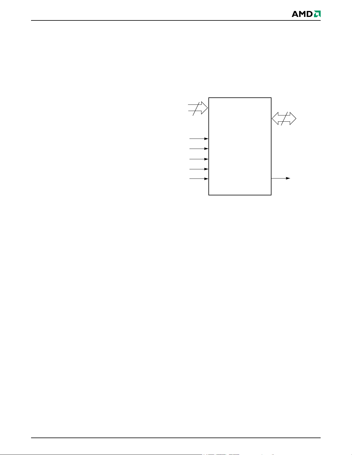
Logic Symbol
19
A0–A18
DQ0–DQ15
CE#
OE#
WE#
RESET
BYTE# RY/BY#
16 or 8
(A-1)
OE# = Output enable
WE# = Write enable
RESET# = Hardware reset pin, active low
RY/BY# = Ready/Busy# output
January 21, 2005 Am29LV800D_00_A4_E Am29LV800D 7
Page 10
PRELIMINARY
Ordering Information
Standard Products
AMD standard products are available in several packages and operating ranges. The order number
(Valid Combination) is formed by a combination of the elements below.
Am29LV800D T -70 E C
TEMPERATURE RANGE
C = Commercial (0°C to +70°C)
D = Commercial (0°C to +70°C) with Pb-Free Package
I = Industrial (–40°C to +85°C)
F = Industrial (–40°C to +85°C) with Pb-Free Package
PACKAGE TYPE
E = 48-Pin Thin Small Outline Package (TSOP) Standard Pinout
(TS 048)
F = 48-Pin Thin Small Outline Package (TSOP) Reverse Pinout
(TSR048)
S = 44-Pin Small Outline Package (SO 044)
WB = 48-Ball Fine Pitch Ball Grid Array (FBGA)
0.80 mm pitch, 6 x 9 mm package (FBB048)
WC = 48-Ball Fine Pitch Ball Grid Array (FBGA)
= 0.80 mm pitch, 6.15 x 8.15 mm package (VBK 048)
SPEED OPTION
See Product Selector Guide and Valid Combinations
BOOT CODE SECTOR ARCHITECTURE
T = Top sector
B = Bottom sector
DEVICE NUMBER/DESCRIPTION
Am29LV800D
8 Megabit (1 M x 8-Bit/512 K x 16-Bit) CMOS Flash Memory
3.0 Volt-only Read, Program, and Erase
Valid Combinations for TSOP and SO Packages
AM29LV800DT-70,
AM29LV800DB-70
AM29LV800DT-90,
AM29LV800DB-90
AM29LV800DT-120,
EC, EI, ED, EF, FC, FD, FF, FI,
SC, SD, SF, SI
EC, EI, ED,EF,FD, FF,FC,
FI,SD, SFSC, SI
AM29LV800DB-120
8Am29LV800DAm29LV800D_00_A4_E January 21, 2005
Page 11
PRELIMINARY
Valid Combinations for FBGA Packages
Order Number Package Marking
WBC
WBI
WBD
AM29LV800DT-70,
AM29LV800DB-70
AM29LV800DT-90,
AM29LV800DB-90
AM29LV800DT-120,
AM29LV800DB-120
WBF
WCC
WCI
WCD
WCF
WCC
WCI
WCD
WCF
WBC
WBI
WBD
WBF
WBC
WBI
WBD
WBF
L800DT70V,
L800DB70V
L800DT90V,
L800DB90V
L800DT12V,
L800DB12V
C, I,
D,F
Valid Combinations
Valid Combinations list configurations planned to be supported in volume for this device. Consult the local AMD
sales office to confirm availability of specific valid combinations and to check on newly released combinations.
January 21, 2005 Am29LV800D_00_A4_E Am29LV800D 9
Page 12
PRELIMINARY
Device Bus Operations
This section describes the requirements and use
of the device bus operations, which are initiated
through the internal command register. The
command register itself does not occupy any
addressable memory location. The register is
composed of latches that store the commands,
along with the address and data information
needed to execute the command. The contents
Table 1. Am29LV800D Device Bus Operations
OE#WE#RESET#Addresses
Operation CE#
Read L L H H A
Write L H L H A
Standby
Output Disable L H H H X High-Z High-Z High-Z
Reset X X X L X High-Z High-Z High-Z
Sector Protect (Note 2) L H L V
Sector Unprotect (Note 2) L H L V
Temporary Sector Unprotect X X X V
Legend:
L = Logic Low = VIL, H = Logic High = VIH, VID = 12.0 ± 0.5 V, X = Don’t Care, AIN = Address In, DIN = Data In, D
Notes:
1. Addresses are A18:A0 in word mode (BYTE# = VIH), A18:A-1 in byte mode (BYTE# = VIL).
2. The sector protect and sector unprotect functions may also be implemented via programming equipment. See
the “Sector Protection/Unprotection” section.
VCC ±
0.3 V
X X
VCC ±
0.3 V
of the register serve as inputs to the internal
state machine. The state machine outputs
dictate the function of the device. Ta b le 1 lists
the device bus operations, the inputs and
control levels they require, and the resulting
output. The following subsections describe each
of these operations in further detail.
DQ8–DQ15
BYTE
#
= V
IH
D
DQ8–DQ14 = High-
OUT
D
IN
X X
X X
D
IN
Z, DQ15 = A-1
BYTE#
= V
High-Z
OUT
(Note 1)
Sector Address,
A6 = L, A1 = H,
ID
Sector Address,
A6 = H, A1 = H,
ID
ID
DQ0–
DQ7
IN
IN
X High-Z High-Z High-Z
A0 = L
A0 = L
A
IN
D
OUT
D
D
D
D
IN
IN
IN
IN
IL
= Data Out
Word/Byte Configuration
The BYTE# pin controls whether the device data
I/O pins DQ15–DQ0 operate in the byte or word
configuration. If the BYTE# pin is set at logic ‘1’,
the device is in word configuration, DQ15–DQ0
are active and controlled by CE# and OE#.
If the BYTE# pin is set at logic ‘0’, the device is
in byte configuration, and only data I/O pins
DQ0–DQ7 are active and controlled by CE# and
OE#. The data I/O pins DQ8–DQ14 are
tri-stated, and the DQ15 pin is used as an input
for the LSB (A-1) address function.
Requirements for Reading Array Data
To read array data from the outputs, the system
must drive the CE# and OE# pins to VIL. CE# is
the power control and selects the device. OE# is
the output control and gates array data to the
output pins. WE# should remain at V
. The
IH
BYTE# pin determines whether the device
outputs array data in words or bytes.
The internal state machine is set for reading
array data upon device power-up, or after a
hardware reset. This ensures that no spurious
alteration of the memory content occurs during
the power transition. No command is necessary
in this mode to obtain array data. Standard
microprocessor read cycles that assert valid
addresses on the device address inputs produce
valid data on the device data outputs. The
device remains enabled for read access until the
command register contents are altered.
See “Reading Array Data” for more information.
Refer to the AC Read Operations table for timing
specifications and to Figure 1 for the timing diagram. I
in the DC Characteristics table repre-
CC1
sents the active current specification for reading
array data.
10 Am29LV800D Am29LV800D_00_A4_E January 21, 2005
Page 13

PRELIMINARY
Writing Commands/Command Sequences
To write a command or command sequence
(which includes programming data to the device
and erasing sectors of memory), the system
must drive WE# and CE# to VIL, and OE# to
VIH.
For program operations, the BYTE# pin determines whether the device accepts program data
in bytes or words. Refer to “Word/Byte Configuration” for more information.
The device features an Unlock Bypass mode to
facilitate faster programming. Once the device
enters the Unlock Bypass mode, only two write
cycles are required to program a word or byte,
instead of four. The “Word/Byte Program
Command Sequence” section has details on programming data to the device using both standard and Unlock Bypass command sequences.
An erase operation can erase one sector, multiple sectors, or the entire device. Tables 2 and
3 indicate the address space that each sector
occupies. A “sector address” consists of the
address bits required to uniquely select a sector.
The “Command Definitions” section has details
on erasing a sector or the entire chip, or suspending/resuming the erase operation.
After the system writes the autoselect command
sequence, the device enters the autoselect
mode. The system can then read autoselect
codes from the internal register (which is separate from the memory array) on DQ7–DQ0.
Standard read cycle timings apply in this mode.
Refer to the “Autose lect Mod e” and “Autosele ct
Command Sequence” sections for more information.
I
in the DC Characteristics table represents
CC2
the active current specification for the write
mode. The
“AC Characteristics” section contains
timing specification tables and timing diagrams
for write operations.
Program and Erase Operation Status
During an erase or program operation, the
system may check the status of the operation by
reading the status bits on DQ7–DQ0. Standard
read cycle timings and ICC read specifications
apply. Refer to “Write Operation Status” for
more information, and to “AC Characteristics”
for timing diagrams.
Standby Mode
When the system is not reading or writing to the
device, it can place the device in the standby
mode. In this mode, current consumption is
greatly reduced, and the outputs are placed in
the high impedance state, independent of the
OE# input.
The device enters the CMOS standby mode
when the CE# and RESET# pins are both held at
V
± 0.3 V. (Note that this is a more restricted
CC
voltage range than VIH.) If CE# and RESET# are
held at VIH, but not within V
± 0.3 V, the device
CC
will be in the standby mode, but the standby
current will be greater. The device requires stan
dard access time (tCE) for read access when the
device is in either of these standby modes,
before it is ready to read data.
If the device is deselected during erasure or programming, the device draws active current until
the operation is completed.
In the DC Characteristics table, I
CC3
and I
CC4
represents the standby current specification.
Automatic Sleep Mode
The automatic sleep mode minimizes Flash
device energy consumption. The device automatically enables this mode when addresses
remain stable for t
+ 30 ns. The automatic
ACC
sleep mode is independent of the CE#, WE#,
and OE# control signals. Standard address
access timings provide new data when
addresses are changed. While in sleep mode,
output data is latched and always available to
the system. I
in the DC Characteristics table
CC4
represents the automatic sleep mode current
specification.
RESET#: Hardware Reset Pin
The RESET# pin provides a hardware method of
resetting the device to reading array data. When
the RESET# pin is driven low for at least a
period of tRP, the device immediately termi-
nates any operation in progress, tristates all
output pins, and ignores all read/write com
mands for the duration of the RESET# pulse.
The device also resets the internal state
machine to reading array data. The operation
that was interrupted should be reinitiated once
the device is ready to accept another command
sequence, to ensure data integrity.
Current is reduced for the duration of the
RESET# pulse. When RESET# is held at
VSS±0.3 V, the device draws CMOS standby
current (I
). If RESET# is held at VIL but not
CC4
within VSS±0.3 V, the standby current will be
greater.
The RESET# pin may be tied to the system reset
circuitry. A system reset would thus also reset
the Flash memory, enabling the system to read
the boot-up firmware from the Flash memory.
-
January 21, 2005 Am29LV800D_00_A4_E Am29LV800D 11
Page 14
PRELIMINARY
If RES E T # is a sserte d duri n g a p r o g ram or e rase
operation, the RY/BY# pin remains a “0” (busy)
until the internal reset operation is complete,
which requires a time of t
READY
(during
Embedded Algorithms). The system can thus
monitor RY/BY# to determine whether the reset
operation is complete. If RESET# is asserted
when a program or erase operation is not exe
cuting (RY/BY# pin is “1”), the reset operation
is completed within a time of t
READY
(not during
Embedded Algorithms). The system can read
data tRH after the RESET# pin returns to VIH.
Refer to the AC Characteristics tables for
RESET# parameters and to Figure 1 for the
timing diagram.
Output Disable Mode
When the OE# input is at VIH, output from the
device is disabled. The output pins are placed in
the high impedance state.
Table 2. Am29LV800DT Top Boot Block Sector Addresses
Sector Size
(Kbytes/
Sector A18 A17 A16 A15 A14 A13 A12
SA0 0 0 0 0 X X X 64/32 00000h–0FFFFh 00000h–07FFFh
SA1 0 0 0 1 X X X 64/32 10000h–1FFFFh 08000h–0FFFFh
SA2 0 0 1 0 X X X 64/32 20000h–2FFFFh 10000h–17FFFh
SA3 0 0 1 1 X X X 64/32 30000h–3FFFFh 18000h–1FFFFh
SA4 0 1 0 0 X X X 64/32 40000h–4FFFFh 20000h–27FFFh
SA5 0 1 0 1 X X X 64/32 50000h–5FFFFh 28000h–2FFFFh
SA6 0 1 1 0 X X X 64/32 60000h–6FFFFh 30000h–37FFFh
SA7 0 1 1 1 X X X 64/32 70000h–7FFFFh 38000h–3FFFFh
SA8 1 0 0 0 X X X 64/32 80000h–8FFFFh 40000h–47FFFh
SA9 1 0 0 1 X X X 64/32 90000h–9FFFFh 48000h–4FFFFh
SA10 1 0 1 0 X X X 64/32 A0000h–AFFFFh 50000h–57FFFh
SA11 1 0 1 1 X X X 64/32 B0000h–BFFFFh 58000h–5FFFFh
SA12 1 1 0 0 X X X 64/32 C0000h–CFFFFh 60000h–67FFFh
SA13 1 1 0 1 X X X 64/32 D0000h–DFFFFh 68000h–6FFFFh
SA14 1 1 1 0 X X X 64/32 E0000h–EFFFFh 70000h–77FFFh
SA15 1 1 1 1 0 X X 32/16 F0000h–F7FFFh 78000h–7BFFFh
SA16 1 1 1 1 1 0 0 8/4 F8000h–F9FFFh 7C000h–7CFFFh
SA17 1 1 1 1 1 0 1 8/4 FA000h–FBFFFh 7D000h–7DFFFh
SA18 1 1 1 1 1 1 X 16/8 FC000h–FFFFFh 7E000h–7FFFFh
Kwords)
Address Range (in hexadecimal)
(x8)
Address Range
(x16)
Address Range
12 Am29LV800D Am29LV800D_00_A4_E January 21, 2005
Page 15
PRELIMINARY
Table 3. Am29LV800DB Bottom Boot Block Sector Addresses
Sector Size
(Kbytes/
Sector A18 A17 A16 A15 A14 A13 A12
SA0 0 0 0 0 0 0 X 16/8 00000h–03FFFh 00000h–01FFFh
SA1 0 0 0 0 0 1 0 8/4 04000h–05FFFh 02000h–02FFFh
SA2 0 0 0 0 0 1 1 8/4 06000h–07FFFh 03000h–03FFFh
SA3 0 0 0 0 1 X X 32/16 08000h–0FFFFh 04000h–07FFFh
SA4 0 0 0 1 X X X 64/32 10000h–1FFFFh 08000h–0FFFFh
SA5 0 0 1 0 X X X 64/32 20000h–2FFFFh 10000h–17FFFh
SA6 0 0 1 1 X X X 64/32 30000h–3FFFFh 18000h–1FFFFh
SA7 0 1 0 0 X X X 64/32 40000h–4FFFFh 20000h–27FFFh
SA8 0 1 0 1 X X X 64/32 50000h–5FFFFh 28000h–2FFFFh
SA9 0 1 1 0 X X X 64/32 60000h–6FFFFh 30000h–37FFFh
SA10 0 1 1 1 X X X 64/32 70000h–7FFFFh 38000h–3FFFFh
SA11 1 0 0 0 X X X 64/32 80000h–8FFFFh 40000h–47FFFh
SA12 1 0 0 1 X X X 64/32 90000h–9FFFFh 48000h–4FFFFh
SA13 1 0 1 0 X X X 64/32 A0000h–AFFFFh 50000h–57FFFh
SA14 1 0 1 1 X X X 64/32 B0000h–BFFFFh 58000h–5FFFFh
SA15 1 1 0 0 X X X 64/32 C0000h–CFFFFh 60000h–67FFFh
SA16 1 1 0 1 X X X 64/32 D0000h–DFFFFh 68000h–6FFFFh
SA17 1 1 1 0 X X X 64/32 E0000h–EFFFFh 70000h–77FFFh
SA18 1 1 1 1 X X X 64/32 F0000h–FFFFFh 78000h–7FFFFh
Kwords)
Address Range (in hexadecimal)
(x8)
Address Range
(x16)
Address Range
Note for Tab l e s 2 and 3: Address range is A18:A-1 in byte mode and A18:A0 in word mode. See “Word/Byte
Configuration” section.
Autoselect Mode
The autoselect mode provides manufacturer
and device identification, and sector protection
verification, through identifier codes output on
DQ7–DQ0. This mode is primarily intended for
programming equipment to automatically
match a device to be programmed with its corresponding programming algorithm. However,
the autoselect codes can also be accessed insystem through the command register.
When using programming equipment, the
autoselect mode requires VID (11.5 V to 12.5 V)
on address pin A9. Address pins A6, A1, and A0
must be as shown in Ta bl e 4. In addition, when
verifying sector protection, the sector address
must appear on the appropriate highest order
address bits (see Tables 2 and 3). Tab le 4 shows
the remaining address bits that are don’t care.
When all necessary bits have been set as
required, the programming equipment may
then read the corresponding identifier code on
DQ7–DQ0.
To access the autoselect codes in-system, the
host system can issue the autoselect command
via the command register, as shown in Tab le 5 .
This method does not require VID. See “Command Definitions” for details on using the
autoselect mode.
January 21, 2005 Am29LV800D_00_A4_E Am29LV800D 13
Page 16
Table 4. Am29LV800D Autoselect Codes (High Voltage Method)
Description Mode CE# OE#
PRELIMINARY
A1
A1
8
1
to
WE
#
A1
2
to
A1
0
A9
A8
to
A7
A6
A5
to
A2
A1 A0
DQ8
to
DQ15
DQ7
to
DQ0
Manufacturer ID: AMD L L H X X V
Device ID:
Am29LV800B
(Top Boot Block)
Device ID:
Am29LV800B
(Bottom Boot
Block)
Sector Protection
Verification
L = Logic Low = VIL, H = Logic High = VIH, SA = Sector Address, X = Don’t care.
Word L L H
X X V
Byte L L H X DAh
Word L L H
X X V
Byte L L H X 5Bh
L L H SA X V
Sector Protection/Unprotection
The hardware sector protection feature disables
both program and erase operations in any
sector. The hardware sector unprotection
feature re-enables both program and erase
operations in previously protected sectors.
The device is shipped with all sectors unprotected. AMD offers the option of programming
and protecting sectors at its factory prior to
shipping the device through AMD’s Express
Flash™ Service. Contact an AMD representative
for details.
It is possible to determine whether a sector is
protected or unprotected. See “Autoselect
Mode” for details.
Sector Protection/unprotection can be implemented via two methods.
The primary method requires VID on the
RESET# pin only, and can be implemented
either in-system or via programming equipment. Figure 2 shows the algorithms and Figure
-
X L X L L X 01h
ID
X L X L H
ID
X L X L H
ID
X L X H L
ID
standard microprocessor bus cycle timing. For
sector unprotect, all unprotected sectors must
first be protected prior to the first sector unprotect write cycle.
The alternate method intended only for programming equipment requires VID on address
pin A9 and OE#. This method is compatible with
programmer routines written for earlier 3.0 voltonly AMD flash devices. Publication number
20536 contains further details; contact an AMD
representative to request a copy.
Temporary Sector Unprotect
This feature allows temporary unprotection of
previously protected sectors to change data
in-system. The Sector Unprotect mode is acti
vated by setting the RESET# pin to VID. During
this mode, formerly protected sectors can be
programmed or erased by selecting the sector
addresses. Once VID is removed from the
RESET# pin, all the previously protected sectors
are protected again. Figure 1 shows the algo-
1 shows the timing diagram. This method uses
22h DAh
22h 5Bh
X
X
01h
(protected)
00h
(unprotecte
d)
-
14 Am29LV800D Am29LV800D_00_A4_E January 21, 2005
Page 17

PRELIMINARY
rithm, and Figure 1 shows the timing diagrams,
for this feature.
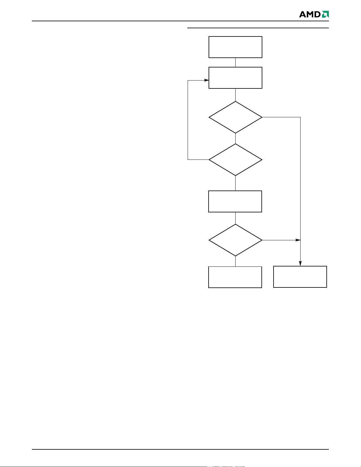
START
RESET# = V
(Note 1)
Perform Erase or
Program Operations
RESET# = V
Temporary Sector
Unprotect Completed
(Note 2)
Notes:
1. All protected sectors unprotected.
2. All previously protected sectors are protected
once again.
ID
IH
Figure 1. Temporary Sector Unprotect
Operation
January 21, 2005 Am29LV800D_00_A4_E Am29LV800D 15
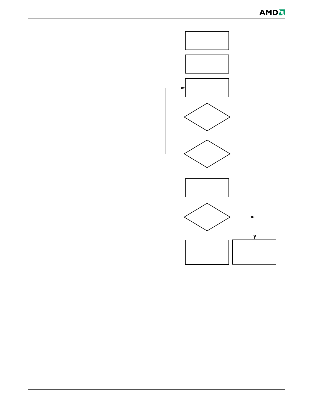
Page 18

PRELIMINARY
Temporary Sector
Unprotect Mode
Increment
PLSCNT
No
PLSCNT
= 25?
Yes
Device failed
Sector Protect
Algorithm
START
PLSCNT = 1
RESET# = V
Wait 1 ms
No
First Write
Cycle = 60h?
Yes
Set up sector
address
Sector Protect:
Write 60h to sector
address with
A6 = 0, A1 = 1,
A0 = 0
Wait 150 s
Verify Sector
Protect: Write 40h
to sector address
with A6 = 0,
A1 = 1, A0 = 0
Read from
sector address
with A6 = 0,
A1 = 1, A0 = 0
No
Data = 01h?
Yes
Protect another
sector?
No
Remove V
from RESET#
Write reset
command
Sector Protect
complete
START
Protect all sectors:
The indicated portion
of the sector protect
ID
Reset
PLSCNT = 1
Yes
ID
algorithm must be
performed for all
unprotected sectors
prior to issuing the
first sector
unprotect address
Increment
PLSCNT
No
PLSCNT
= 1000?
Yes
Device failed
Sector Unprotect
PLSCNT = 1
RESET# = V
Wait 1 ms
First Write
Cycle = 60h?
Yes
No
All sectors
protected?
Yes
Set up first sector
address
Sector Unprotect:
Write 60h to sector
address with
A6 = 1, A1 = 1,
A0 = 0
Wait 15 ms
Verify Sector
Unprotect: Write
40h to sector
address with
A6 = 1, A1 = 1,
A0 = 0
Read from
sector address
with A6 = 1,
A1 = 1, A0 = 0
No
Data = 00h?
Yes
Last sector
verified?
Yes
Remove V
from RESET#
ID
ID
No
Temporary Sector
No
Unprotect Mode
Set up
next sector
address
Algorithm
Write reset
command
Sector Unprotect
complete
Figure 2. In-System Sector Protect/
Sector Unprotect Algorithms
16 Am29LV800D Am29LV800D_00_A4_E January 21, 2005
Page 19

PRELIMINARY
Hardware Data Protection
The command sequence requirement of unlock
cycles for programming or erasing provides data
protection against inadvertent writes (refer to
Tab le 5 for command definitions). In addition,
the following hardware data protection measures prevent accidental erasure or programming, which might otherwise be caused by
spurious system level signals during V
CC
power-up and power-down transitions, or from
system noise.
Low VCC Write Inhibit
When VCC is less than V
, the device does not
LKO
accept any write cycles. This protects data
during V
power-up and power-down. The
CC
command register and all internal program/erase circuits are disabled, and the device
resets. Subsequent writes are ignored until V
is greater than V
. The system must provide
LKO
CC
Command Definitions
Writing specific address and data commands or
sequences into the command register initiates
device operations. Ta b le 5 defines the valid register command sequences. Writing incorrect
address and data values or writing them in
the improper sequence resets the device to
reading array data.
All addresses are latched on the falling edge of
WE# or CE#, whichever happens later. All data
is latched on the rising edge of WE# or CE#,
whichever happens first. Refer to the appropriate timing diagrams in the “AC Characteristics” section.
Reading Array Data
The device is automatically set to reading array
data after device power-up. No commands are
required to retrieve data. The device is also
ready to read array data after completing an
Embedded Program or Embedded Erase algo
rithm.
After the device accepts an Erase Suspend command, the device enters the Erase Suspend
mode. The system can read array data using the
standard read timings, except that if it reads at
an address within erase-suspended sectors, the
device outputs status data. After completing a
programming operation in the Erase Suspend
mode, the system may once again read array
data with the same exception. See “Erase Suspend/Erase Resume Commands” for more information on this mode.
The system must issue the reset command to
re-enable the device for reading array data if
-
the proper signals to the control pins to prevent
unintentional writes when V
V
.
LKO
Write Pulse “Glitch” Protection
is greater than
CC
Noise pulses of less than 5 ns (typical) on OE#,
CE# or WE# do not initiate a write cycle.
Logical Inhibit
Write cycles are inhibited by holding any one of
OE# = VIL, CE# = VIH or WE# = VIH. To initiate
a write cycle, CE# and WE# must be a logical
zero while OE# is a logical one.
Power-Up Write Inhibit
If WE# = CE# = VIL and OE# = VIH during
power up, the device does not accept commands on the rising edge of WE#. The internal
state machine is automatically reset to reading
array data on power-up.
DQ5 goes high, or while in the autoselect mode.
See the “Reset Command” section, next.
See also “Requirements for Reading Array Data”
in the “Device Bus Operations” section for more
information. The Read Operations table provides
the read parameters, and Figure 1 shows the
timing diagram.
Reset Command
Writing the reset command to the device resets
the device to reading array data. Address bits
are don’t care for this command.
The reset command may be written between the
sequence cycles in an erase command sequence
before erasing begins. This resets the device to
reading array data. Once erasure begins, however, the device ignores reset commands until
the operation is complete.
The reset command may be written between the
sequence cycles in a program command
sequence before programming begins. This
resets the device to reading array data (also
applies to programming in Erase Suspend
mode). Once programming begins, however, the
device ignores reset commands until the operation is complete.
The reset command may be written between the
sequence cycles in an autoselect command
sequence. Once in the autoselect mode, the
reset command must be written to return to
reading array data (also applies to autoselect
during Erase Suspend).
January 21, 2005 Am29LV800D_00_A4_E Am29LV800D 17
Page 20

PRELIMINARY
If DQ5 goes high during a program or erase
operation, writing the reset command returns
the device to reading array data (also applies
during Erase Suspend).
Autoselect Command Sequence
The autoselect command sequence allows the
host system to access the manufacturer and
devices codes, and determine whether or not a
sector is protected. Ta bl e 5 shows the address
and data requirements. This method is an alternative to that shown in Tab le 4 , which is
intended for PROM programmers and requires
VID on address bit A9.
The autoselect command sequence is initiated
by writing two unlock cycles, followed by the
autoselect command. The device then enters
the autoselect mode, and the system may read
at any address any number of times, without
initiating another command sequence.
A read cycle at address XX00h retrieves the
manufacturer code. A read cycle at address
XX01h in word mode (or 02h in byte mode)
returns the device code. A read cycle containing
a sector address (SA) and the address 02h in
word mode (or 04h in byte mode) returns 01h if
that sector is protected, or 00h if it is unprotected. Refer to Tables 2 and 3 for valid sector
addresses.
The system must write the reset command to
exit the autoselect mode and return to reading
array data.
Word/Byte Program Command Sequence
The system may program the device by word or
byte, depending on the state of the BYTE# pin.
Programming is a four-bus-cycle operation. The
program command sequence is initiated by
writing two unlock write cycles, followed by the
program set-up command. The program
address and data are written next, which in turn
initiate the Embedded Program algorithm. The
system is not required to provide further con
trols or timings. The device automatically provides internally generated program pulses and
verifies the programmed cell margin. Ta b le 5
shows the address and data requirements for
the byte program command sequence.
-
“Write Operation Status” for information on
these status bits.
Any commands written to the device during the
Embedded Program Algorithm are ignored. Note
that a hardware reset immediately terminates
the programming operation. The program
command sequence should be reinitiated once
the device has reset to reading array data, to
ensure data integrity.
Programming is allowed in any sequence and
across sector boundaries. A bit cannot be pro-
grammed from a “0” back to a “1”.
Attempting to do so may halt the operation and
set DQ5 to “1”, or cause the Data# Polling algorithm to indicate the operation was successful.
However, a succeeding read will show that the
data is still “0”. Only erase operations can
convert a “0” to a “1”.
Unlock Bypass Command Sequence
The unlock bypass feature allows the system to
program bytes or words to the device faster
than using the standard program command
sequence. The unlock bypass command
sequence is initiated by first writing two unlock
cycles. This is followed by a third write cycle
containing the unlock bypass command, 20h.
The device then enters the unlock bypass mode.
A two-cycle unlock bypass program command
sequence is all that is required to program in
this mode. The first cycle in this sequence con
tains the unlock bypass program command,
A0h; the second cycle contains the program
address and data. Additional data is programmed in the same manner. This mode dispenses with the initial two unlock cycles
required in the standard program command
sequence, resulting in faster total programming
Tab le 5 shows the requirements for the
time.
command sequence.
During the unlock bypass mode, only the Unlock
Bypass Program and Unlock Bypass Reset commands are valid. To exit the unlock bypass
mode, the system must issue the two-cycle
unlock bypass reset command sequence. The
first cycle must contain the data 90h; the
second cycle the data 00h. Addresses are don’t
care for both cycles. The device then returns to
reading array data.
-
When the Embedded Program algorithm is complete, the device then returns to reading array
data and addresses are no longer latched. The
system can determine the status of the program
operation by using DQ7, DQ6, or RY/BY#. See
18 Am29LV800D Am29LV800D_00_A4_E January 21, 2005
Figure 1 illustrates the algorithm for the
program operation. See the Erase/Program
Operations table in “AC Characteristics” for
parameters, and to Figure 1 for timing diagrams.
Page 21

Embedded
Program
algorithm
in progress
PRELIMINARY
START
Write Program
Command Sequence
Data Poll
from System
tion. The Chip Erase command sequence should
be reinitiated once the device has returned to
reading array data, to ensure data integrity.
The system can determine the status of the
erase operation by using DQ7, DQ6, DQ2, or
RY/BY#. See “Write Operation Status” for information on these status bits. When the
Embedded Erase algorithm is complete, the
device returns to reading array data and
addresses are no longer latched.
Figure 1 illustrates the algorithm for the erase
operation. See the Erase/Program Operations
tables in “AC Characteristics” for parameters,
and to Figure 1 for timing diagrams.
Verify Data?
Yes
Increment Address
Note: See Table 5 for program command sequence.
No
Last Address?
Yes
Programming
Completed
No
Figure 1. Program Operation
Chip Erase Command Sequence
Chip erase is a six bus cycle operation. The chip
erase command sequence is initiated by writing
two unlock cycles, followed by a set-up com
mand. Two additional unlock write cycles are
then followed by the chip erase command,
which in turn invokes the Embedded Erase algo-
rithm. The device does not require the system
to preprogram prior to erase. The Embedded
Erase algorithm automatically preprograms and
verifies the entire memory for an all zero data
pattern prior to electrical erase. The system is
not required to provide any controls or timings
during these operations. Tab le 5 shows the
address and data requirements for the chip
erase command sequence.
Any commands written to the chip during the
Embedded Erase algorithm are ignored. Note
that a hardware reset during the chip erase
operation immediately terminates the opera
-
-
Sector Erase Command Sequence
Sector erase is a six bus cycle operation. The
sector erase command sequence is initiated by
writing two unlock cycles, followed by a set-up
command. Two additional unlock write cycles
are then followed by the address of the sector to
be erased, and the sector erase command.
5 shows the address and data requirements for
the sector erase command sequence.
The device does not require the system to pre-
program the memory prior to erase. The
Embedded Erase algorithm automatically programs and verifies the sector for an all zero data
pattern prior to electrical erase. The system is
not required to provide any controls or timings
during these operations.
After the command sequence is written, a sector
erase time-out of 50 µs begins. During the timeout period, additional sector addresses and
sector erase commands may be written.
Loading the sector erase buffer may be done in
any sequence, and the number of sectors may
be from one sector to all sectors. The time
between these additional cycles must be less
than 50 µs, otherwise the last address and
command might not be accepted, and erasure
may begin. It is recommended that processor
interrupts be disabled during this time to ensure
all commands are accepted. The interrupts can
be re-enabled after the last Sector Erase
command is written. If the time between addi
tional sector erase commands can be assumed
to be less than 50 µs, the system need not
monitor DQ3. Any command other than
Sector Erase or Erase Suspend during the
time-out period resets the device to
reading array data. The system must rewrite
the command sequence and any additional
sector addresses and commands.
Ta b le
-
January 21, 2005 Am29LV800D_00_A4_E Am29LV800D 19
Page 22

PRELIMINARY
The system can monitor DQ3 to determine if the
sector erase timer has timed out. (See the
“DQ3: Sector Erase Timer” section.) The timeout begins from the rising edge of the final WE#
pulse in the command sequence.
Once the sector erase operation has begun, only
the Erase Suspend command is valid. All other
commands are ignored. Note that a hardware
reset during the sector erase operation imme
diately terminates the operation. The Sector
Erase command sequence should be reinitiated
once the device has returned to reading array
data, to ensure data integrity.
When the Embedded Erase algorithm is complete, the device returns to reading array data
and addresses are no longer latched. The
system can determine the status of the erase
operation by using DQ7, DQ6, DQ2, or RY/BY#.
Refer to “Write Operation Status” for information on these status bits.
Figure 1 illustrates the algorithm for the erase
operation. Refer to the Erase/Program Operations tables in the “AC Characteristics” section
for parameters, and to Figure 1 for timing diagrams.
-
Erase Suspend/Erase Resume Commands
The Erase Suspend command allows the system
to interrupt a sector erase operation and then
read data from, or program data to, any sector
not selected for erasure. This command is valid
only during the sector erase operation, including
the 50 µs time-out period during the sector
erase command sequence. The Erase Suspend
command is ignored if written during the chip
erase operation or Embedded Program algo
rithm. Writing the Erase Suspend command
during the Sector Erase time-out immediately
terminates the time-out period and suspends
the erase operation. Addresses are
“don’t-cares” when writing the Erase Suspend
command.
-
When the Erase Suspend command is written
during a sector erase operation, the device
requires a maximum of 20 µs to suspend the
erase operation. However, when the Erase
Suspend command is written during the sector
erase time-out, the device immediately termi
nates the time-out period and suspends the
erase operation.
After the erase operation has been suspended,
the system can read array data from or program
data to any sector not selected for erasure. (The
device “erase suspends” all sectors selected for
erasure.) Normal read and write timings and
command definitions apply. Reading at any
address within erase-suspended sectors pro
duces status data on DQ7–DQ0. The system can
use DQ7, or DQ6 and DQ2 together, to deter
mine if a sector is actively erasing or is erasesuspended. See
information on these status bits.
After an erase-suspended program operation is
complete, the system can once again read array
data within non-suspended sectors. The system
can determine the status of the program operation using the DQ7 or DQ6 status bits, just as in
the standard program operation. See
Operation Status” for more information.
The system may also write the autoselect
command sequence when the device is in the
Erase Suspend mode. The device allows reading
autoselect codes even at addresses within
erasing sectors, since the codes are not stored
in the memory array. When the device exits the
autoselect mode, the device reverts to the Erase
Suspend mode, and is ready for another valid
operation. See “Autoselect Command
Sequence” for more information.
The system must write the Erase Resume
command (address bits are “don’t care”) to exit
the erase suspend mode and continue the sector
erase operation. Further writes of the Resume
command are ignored. Another Erase Suspend
command can be written after the device has
resumed erasing.
“Write Operation Status” for
-
-
-
“Write
20 Am29LV800D Am29LV800D_00_A4_E January 21, 2005
Page 23
START
Write Erase
Command Sequence
Data Poll
from System
No
Data = FFh?
Erasure Completed
PRELIMINARY
Embedded
Erase
algorithm
in progress
Yes
Notes:
1. See Table 5 for erase command sequenc e.
2. See “DQ3: Sector Erase Timer” for more information.
Figure 1. Erase Operation
Table 5. Am29LV800D Command Definitions
Command
Sequence
(Note 1)
Read (Note 6) 1 RA RD
Reset (Note 7) 1 XXX F0
Manufacturer ID
Device ID,
Top Boot Block
Device ID,
Bottom Boot Block
Sector Protect Verify
Autoselect (Note
(Note 9)
Program
Unlock Bypass
Word
Byte AAA 555 AAA
Word
Byte AAA 555 AAA X02 DA
Word
Byte AAA 555 AAA X02 5B
Word
Byte AAA 555 AAA
Word
Byte AAA 555 AAA
Word
Byte
Unlock Bypass Program (Note
10)
Unlock Bypass Reset (Note
11)
First Second Third Fourth Fifth Sixth
Addr Data Addr Data Addr Data Addr Data Addr Data Addr Data
Cycles
555
4
555
4
555
4
555
4
555
4
555
3
AAA
2AA
AA
2AA
AA
2AA
AA
2AA
AA
2AA
AA
2AA
AA
555 AAA
2 XXX A0 PA PD
2 XXX 90 XXX 00
55
55
55
55
55
55
Bus Cycles (Notes 2-5)
555
555
555
555
555
555
90 X00 01
X01 22DA
90
X01 225B
90
(SA)
X02
90
(SA)
X04
A0 PA PD
20
XX00
XX01
00
01
January 21, 2005 Am29LV800D_00_A4_E Am29LV800D 21
Page 24
PRELIMINARY
Chip Erase
Sector Erase
Erase Suspend (Note 12) 1 XXX B0
Erase Resume (Note 13) 1 XXX 30
Legend:
X = Don’t care
RA = Address of the memory locatio n to be read.
RD = Data read from location RA during read operation.
PA = Address of the memory location to be programmed. Addresses latch on the falling edge of the WE# or CE# pulse,
whichever happens later.
PD = Data to be programmed at location PA. Data latches on the rising edge of WE# or CE# pulse, whichever happens
first.
SA = Address of the sector to be verified (in autoselect mode) or erased. Address bits A18–A12 uniquely select any
sector.
Notes:
1. See Table 1 for description of bus operations.
2. All values are in hexadecimal.
3. Except when reading array or autoselect data, all bus cycles are write operations.
4. Data bits DQ15–DQ8 are don’t cares for unlock and command cycles.
5. Address bits A18–A11 are don’t cares for unlock and command cycles, unless PA or SA required.
6. No unlock or command cycles required when reading array data.
7. The Reset command is r equired to return to reading array data when device is in the autoselect mo de, or if DQ5
goes high (while the device is providing status data).
8. The fourth cycle of the autoselect command sequence is a read cycle.
9. The data is 00h for an un prot ected sect or and 01 h for a protected sec tor. See “Autoselec t Command Sequence” for
more information.
10.The Unlock Bypass command is required prior to the Unlock Bypass Program command.
11.The Unlock Bypass Reset command is required to return to reading array data when the device is in the unlock
bypass mode.
12.The system may read and program in non-erasing sectors, or enter the autoselect mode, when in th e Erase Suspend
mode. The Erase Suspend command is valid only during a sector erase operation.
13.The Erase Resume command is valid only during the Erase Suspend mode.
Word
Byte AAA 555 AAA AAA 555 AAA
Word
Byte AAA 555 AAA AAA 555
555
6
555
6
AA
AA
2AA
2AA
55
55
555
555
80
80
555
555
AA
AA
2AA
2AA
555
55
55 SA 30
10
Write Operation Status
The device provides several bits to determine
the status of a write operation: DQ2, DQ3, DQ5,
DQ6, DQ7, and RY/BY#. Tab le 6 and the following subsections describe the functions of
these bits. DQ7, RY/BY#, and DQ6 each offer a
method for determining whether a program or
erase operation is complete or in progress.
These three bits are discussed first.
DQ7: Data# Polling
The Data# Polling bit, DQ7, indicates to the host
system whether an Embedded Algorithm is in
progress or completed, or whether the device is
in Erase Suspend. Data# Polling is valid after
the rising edge of the final WE# pulse in the
program or erase command sequence.
During the Embedded Program algorithm, the
device outputs on DQ7 the complement of the
22 Am29LV800D Am29LV800D_00_A4_E January 21, 2005
datum programmed to DQ7. This DQ7 status
also applies to programming during Erase Sus
pend. When the Embedded Program algorithm
is complete, the device outputs the datum programmed to DQ7. The system must provide the
program address to read valid status information on DQ7. If a program address falls within a
protected sector, Data# Polling on DQ7 is active
for approximately 1 µs, then the device returns
to reading array data.
During the Embedded Erase algorithm, Data#
Polling produces a “0” on DQ7. When the
Embedded Erase algorithm is complete, or if the
device enters the Erase Suspend mode, Data#
Polling produces a “1” on DQ7. This is analogous
to the complement/true datum output described
for the Embedded Program algorithm: the erase
function changes all the bits in a sector to “1”;
-
Page 25
PRELIMINARY
prior to this, the device outputs the “complement,” or “0.” The system must provide an
address within any of the sectors selected for
erasure to read valid status information on DQ7.
After an erase command sequence is written, if
all sectors selected for erasing are protected,
Data# Polling on DQ7 is active for approximately 100 µs, then the device returns to
reading array data. If not all selected sectors are
protected, the Embedded Erase algorithm
erases the unprotected sectors, and ignores the
selected sectors that are protected.
When the system detects DQ7 has changed
from the complement to true data, it can read
valid data at DQ7–DQ0 on the following read
cycles. This is because DQ7 may change asynchronously with DQ0–DQ6 while Output Enable
(OE#) is asserted low.
Figure 1, Data# Polling
Timings (During Embedded Algorithms), in the
“AC Characteristics” section illustrates this.
No
START
Read DQ7–DQ0
Addr = VA
DQ7 = Data?
No
DQ5 = 1?
Yes
Tab l e 6 shows the outputs for Data# Polling on
DQ7. Figure 1 shows the Data# Polling algorithm.
Yes
Read DQ7–DQ0
Addr = VA
DQ7 = Data?
No
FAIL
Notes:
1. VA = Valid address for programming. During a
sector erase operation, a valid address is an
address within any sector selected for erasure.
During chip erase, a valid address is any
non-protected sector address.
2. DQ7 should be rechecked even if DQ5 = “1” because DQ7 may change simultaneously with DQ5.
Yes
PASS
Figure 1. Data# Polling Algorithm
RY/ BY# : Read y/B usy #
The RY/BY# is a dedicated, open-drain output
pin that indicates whether an Embedded Algorithm is in progress or complete. The RY/BY#
status is valid after the rising edge of the final
WE# pulse in the command sequence. Since
RY/BY# is an open-drain output, several
January 21, 2005 Am29LV800D_00_A4_E Am29LV800D 23
Page 26

PRELIMINARY
RY/BY# pins can be tied together in parallel with
a pull-up resistor to VCC.
If the output is low (Busy), the device is actively
erasing or programming. (This includes programming in the Erase Suspend mode.) If the
output is high (Ready), the device is ready to
read array data (including during the Erase
Suspend mode), or is in the standby mode.
Tab l e 6 shows the outputs for RY/BY#. Figures
1, 1, 1 and 1 shows RY/BY# for read, reset, program, and erase operations, respectively.
DQ6: Toggle Bit I
Toggle Bit I on DQ6 indicates whether an
Embedded Program or Erase algorithm is in
progress or complete, or whether the device has
entered the Erase Suspend mode. Toggle Bit I
may be read at any address, and is valid after
the rising edge of the final WE# pulse in the
command sequence (prior to the program or
erase operation), and during the sector erase
time-out.
During an Embedded Program or Erase algorithm operation, successive read cycles to any
address cause DQ6 to toggle. (The system may
use either OE# or CE# to control the read
cycles.) When the operation is complete, DQ6
stops toggling.
After an erase command sequence is written, if
all sectors selected for erasing are protected,
DQ6 toggles for approximately 100 µs, then
returns to reading array data. If not all selected
sectors are protected, the Embedded Erase
algorithm erases the unprotected sectors, and
ignores the selected sectors that are protected.
The system can use DQ6 and DQ2 together to
determine whether a sector is actively erasing
or is erase-suspended. When the device is
actively erasing (that is, the Embedded Erase
algorithm is in progress), DQ6 toggles. When
the device enters the Erase Suspend mode, DQ6
stops toggling. However, the system must also
use DQ2 to determine which sectors are erasing
or erase-suspended. Alternatively, the system
can use DQ7 (see the subsection on
Data# Polling”).
If a program address falls within a protected
sector, DQ6 toggles for approximately 1 µs after
the program command sequence is written,
then returns to reading array data.
DQ6 also toggles during the erase-suspendprogram mode, and stops toggling once the
Embedded Program algorithm is complete.
“DQ7:
Tab le 6 shows the outputs for Toggle Bit I on
DQ6. Figure 1 shows the toggle bit algorithm.
Figure 1 in the “AC Characteristics” section
shows the toggle bit timing diagrams. Figure 1
shows the differences between DQ2 and DQ6 in
graphical form. See also the subsection on
“DQ2: Toggle Bit II”.
DQ2: Toggle Bit II
The “Toggle Bit II” on DQ2, when used with
DQ6, indicates whether a particular sector is
actively erasing (that is, the Embedded Erase
algorithm is in progress), or whether that sector
is erase-suspended. Toggle Bit II is valid after
the rising edge of the final WE# pulse in the
command sequence.
DQ2 toggles when the system reads at
addresses within those sectors that have been
selected for erasure. (The system may use
either OE# or CE# to control the read cycles.)
But DQ2 cannot distinguish whether the sector
is actively erasing or is erase-suspended. DQ6,
by comparison, indicates whether the device is
actively erasing, or is in Erase Suspend, but
cannot distinguish which sectors are selected for
erasure. Thus, both status bits are required for
sector and mode information. Refer to Ta b le 6 to
compare outputs for DQ2 and DQ6.
Figure 1 shows the toggle bit algorithm in flowchart form, and the section “DQ2: Toggle Bit II”
explains the algorithm. See also the “DQ6:
Tog g le Bi t I” subsection. Figure 1 shows the
toggle bit timing diagram. Figure 1 shows the
differences between DQ2 and DQ6 in graphical
form.
Reading Toggle Bits DQ6/DQ2
Refer to Figure 1 for the following discussion.
Whenever the system initially begins reading
toggle bit status, it must read DQ7–DQ0 at least
twice in a row to determine whether a toggle bit
is toggling. Typically, the system would note and
store the value of the toggle bit after the first
read. After the second read, the system would
compare the new value of the toggle bit with the
first. If the toggle bit is not toggling, the device
has completed the program or erase operation.
The system can read array data on DQ7–DQ0 on
the following read cycle.
However, if after the initial two read cycles, the
system determines that the toggle bit is still
toggling, the system also should note whether
the value of DQ5 is high (see the section on
DQ5). If it is, the system should then determine
again whether the toggle bit is toggling, since
the toggle bit may have stopped toggling just as
24 Am29LV800D Am29LV800D_00_A4_E January 21, 2005
Page 27
PRELIMINARY
DQ5 went high. If the toggle bit is no longer toggling, the device has successfully completed the
program or erase operation. If it is still toggling,
the device did not completed the operation suc
cessfully, and the system must write the reset
command to return to reading array data.
The remaining scenario is that the system initially determines that the toggle bit is toggling
and DQ5 has not gone high. The system may
continue to monitor the toggle bit and DQ5
through successive read cycles, determining the
status as described in the previous paragraph.
Alternatively, it may choose to perform other
system tasks. In this case, the system must
start at the beginning of the algorithm when it
returns to determine the status of the operation
(top of Figure 1).
DQ5: Exceeded Timing Limits
DQ5 indicates whether the program or erase
time has exceeded a specified internal pulse
count limit. Under these conditions DQ5 pro
duces a “1.” This is a failure condition that indicates the program or erase cycle was not
successfully completed.
The DQ5 failure condition may appear if the
system tries to program a “1” to a location that
is previously programmed to “0.” Only an
erase operation can change a “0” back to a
“1.” Under this condition, the device halts the
operation, and when the operation has
exceeded the timing limits, DQ5 produces a “1.”
-
No
START
Read DQ7–DQ0
Read DQ7–DQ0
Toggle Bit
= Toggle?
Yes
DQ5 = 1?
Yes
Read DQ7–DQ0
Twice
Toggle Bit
= Toggle?
(Note 1)
No
(Notes
1, 2)
No
Under both these conditions, the system must
issue the reset command to return the device to
reading array data.
DQ3: Sector Erase Timer
After writing a sector erase command sequence,
the system may read DQ3 to determine whether
or not an erase operation has begun. (The
sector erase timer does not apply to the chip
erase command.) If additional sectors are
selected for erasure, the entire time-out also
applies after each additional sector erase command. When the time-out is complete, DQ3
switches from “0” to “1.” The system may
ignore DQ3 if the system can guarantee that
the time between additional sector erase commands will always be less than 50 µs. See also
the “Sector Erase Command Sequence” section.
After the sector erase command sequence is
written, the system should read the status on
DQ7 (Data# Polling) or DQ6 (Toggle Bit I) to
ensure the device has accepted the command
sequence, and then read DQ3. If DQ3 is “1”, the
internally controlled erase cycle has begun; all
Yes
Program/Erase
Operation Not
Complete, Write
Reset Command
Notes:
1. Read toggle bit twice to determine whether or not
it is toggling. See text.
2. Recheck toggle bit because it may stop toggling
as DQ5 changes to “1”. See te x t .
Program/Erase
Operation Complete
Figure 1. Toggle Bit Algorithm
further commands (other than Erase Suspend)
are ignored until the erase operation is com
plete. If DQ3 is “0”, the device will accept additional sector erase commands. To ensure the
command has been accepted, the system soft
ware should check the status of DQ3 prior to
and following each subsequent sector erase
command. If DQ3 is high on the second status
check, the last command might not have been
accepted. Ta b le 6 shows the outputs for DQ3.
January 21, 2005 Am29LV800D_00_A4_E Am29LV800D 25
Page 28
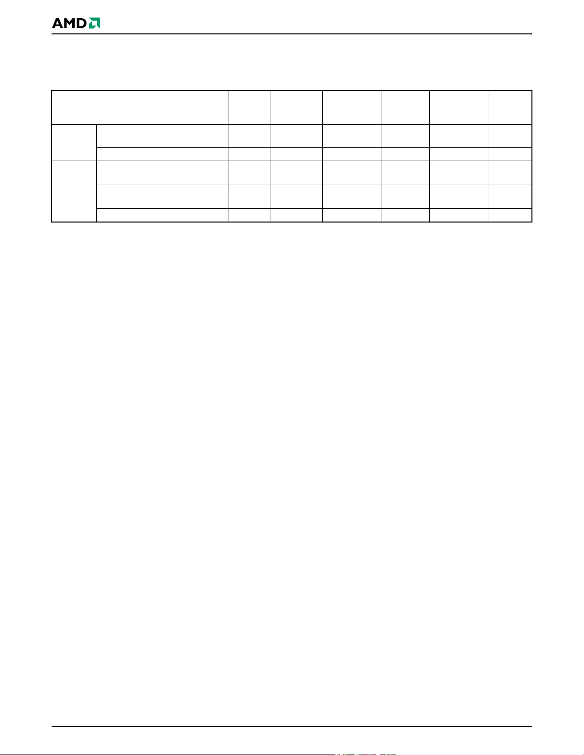
PRELIMINARY
Table 6. Write Operation Status
DQ7
(Note
Operation
Standard
Mode
Erase
Suspend
Mode
Notes:
1. DQ5 switches to ‘1’ wh en an E mbe dd e d Pr og ra m or Emb e dd ed Era s e op er a tio n has exc ee d ed t he max im u m
timing limits. See
2. DQ7 and DQ2 require a valid address when reading status information. Refer to the appropriate subsection
for further details.
Embedded Program
Algorithm
Embedded Erase Algorithm 0 Toggle 0 1 Toggle 0
Reading within Erase
Suspended Sector
Reading within Non-Erase
Suspended Sector
Erase-Suspend-Program DQ7# Toggle 0 N/A N/A 0
“DQ5: Exceeded Timing Limits” for more information.
2) DQ6
DQ7# Toggle 0 N/A No toggle 0
1 No toggle 0 N/A Toggle 1
Data Data Data Data Data 1
DQ5
(Note 1) DQ3
DQ2
(Note 2)
RY/BY
#
26 Am29LV800D Am29LV800D_00_A4_E January 21, 2005
Page 29
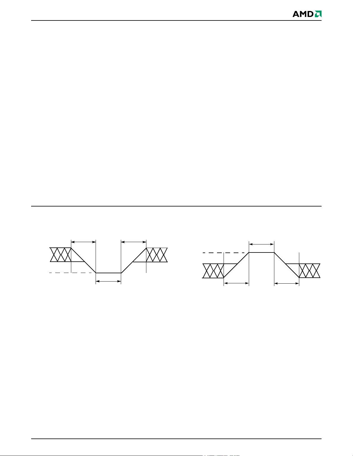
PRELIMINARY
ABSOLUTE MAXIMUM RATINGS
Storage Temperature
Plastic Packages . . . . . . . . . . . . . . . –65°C to +150°C
Ambient Temperature
with Power Applied . . . . . . . . . . . . . . –65°C to +85°C
Volt age with Respect to Ground
1. Minimum DC voltage on input or I/O pins is –0.5 V. During voltage transitions, input or I/O pins may
undershoot V
is VCC +0.5 V. During voltage transitions, input or I/O pins may overshoot to VCC +2.0 V for periods up to 20
ns. See
2. Minimum DC input voltage on pins A9, OE#, and
RESET# is –0.5 V. During voltage transitions, A9,
OE#, and RESET# may under s ho ot VSS to –2.0 V for
periods of up to 20 ns. See
input voltage on pin A9 is + 12.5 V which may
overshoot to 14.0 V for pe riods up to 20 ns.
3. No more than one output m ay be sh orted to gro und
at a time. Duration of the short circuit shou ld not b e
greater than one second.
Stresses above thos e listed under “Absol ute Maximum
Ratings” may c ause perm anent dama ge to the device. T his
is a stress rating only; functional operation of the device at
these or any other conditions above those indicated in the
operational section s of this data sheet is not implied.
Figure 3.
to –2.0 V for periods of up to 20 ns. See Figure 2. Maximum DC voltage on input or I/O pins
SS
Figure 2. Maximum DC
VCC (Note 1). . . . . . . . . . . . . . . . –0.5 V to +4.0 V
A9, OE#, and
RESET# (Note 2) . . . . . . . . . . . –0.5 V to +12.5 V
All other pins (Note 1). . . . . . –0.5 V to VCC+0.5 V
Output Sho r t Ci r cu it C u rre n t (No te 3) . . . . . . . 200 mA
Notes:
Exposure of the device to absolute maximum rating
conditions for extended period s may affe ct dev ice reli abil ity.
Operating Ranges
Commercial (C) Devices
Ambient Temperature (TA) . . . . . . . . . . .0°C to +70°C
Industrial (I) Devices
Ambient Temperature (TA) . . . . . . . . .–40°C to +85°C
VCC Supply Voltages
VCC for regulated voltage range . . . . +3.0 V to +3.6 V
VCC for full voltage range . . . . . . . . . +2.7 V to +3.6 V
Operating ranges define those limits between which the
functionality of the device is guaranteed
20 ns
+0.8 V
–0.5 V
–2.0 V
20 ns
20 ns
Figure 2. Maximum Negative Overshoot
Waveform
20 ns
V
CC
+2.0 V
V
CC
+0.5 V
2.0 V
20 ns
20 ns
Figure 3. Maximum Positive Overshoot
Waveform
January 21, 2005 Am29LV800D_00_A4_E Am29LV800D 27
Page 30

DC Characteristics
CMOS Compatible
Paramete
r
Description Test Conditions Min Typ Max Unit
PRELIMINARY
I
I
I
I
I
I
I
V
V
I
LI
LIT
LO
CC1
CC2
CC3
CC4
CC5
V
IL
IH
ID
Input Load Current
A9 Input Load Current VCC = V
Output Leakage Current
VCC Active Read Current
(Notes 1, 2)
VCC Active Write Current
(Notes 2, 3, 5)
VCC Standby Current (Note
2)
VCC Reset Current (Note 2) RESET# = V
Automatic Sleep Mode
(Notes 2, 4)
VIN = VSS to VCC,
VCC = VCC
V
OUT
VCC = V
CE# = V
V
IH,
max
; A9 = 12.5 V 35 µA
CC max
= VSS to VCC,
CC max
OE#
IL,
=
Byte Mode
5 MHz 7 15
1 MHz 2 4
±1.0 µA
±1.0 µA
mA
CE# = V
V
IH,
Word Mode
CE# = V
IL,
IL,
OE#
OE#
=
= VIH
5 MHz 7 15
1 MHz 2 4
15 30 mA
CE#, RESET# = VCC±0.3 V 0.2 5 µA
± 0.3 V 0.2 5 µA
SS
VIH = V
V
= V
IL
± 0.3 V;
CC
± 0.3 V
SS
0.2 5 µA
Input Low Voltage –0.5 0.8 V
Input High Voltage 0.7 x V
Voltage for Autoselect and
Temporary Sector Unprotect
VCC = 3.3 V 11.5 12.5 V
CC
VCC + 0.3 V
V
V
V
V
OL
OH1
OH2
LKO
Output Low Voltage IOL = 4.0 mA, VCC = V
IOH = –2.0 mA, VCC = V
Output High Voltage
IOH = –100 µA, VCC = V
Low VCC Lock-Out Voltage
(Note 4)
0.45 V
CC min
0.85 V
CC min
CC min
VCC–0.4
CC
2.3 2.5 V
Notes:
1. The ICC current listed is typically less than 2 mA/MHz, with OE# at VIH. Typical VCC is 3.0 V.
2. Maximum ICC specifications are tested with VCC = V
3. ICC active while Embedded Erase or Embedded Program is in progress.
4. Automatic sleep mode enables the low power mode when addresses remain stable for t
CCmax
.
+ 30 ns.
ACC
5. Not 100% tested.
V
28 Am29LV800D Am29LV800D_00_A4_E January 21, 2005
Page 31
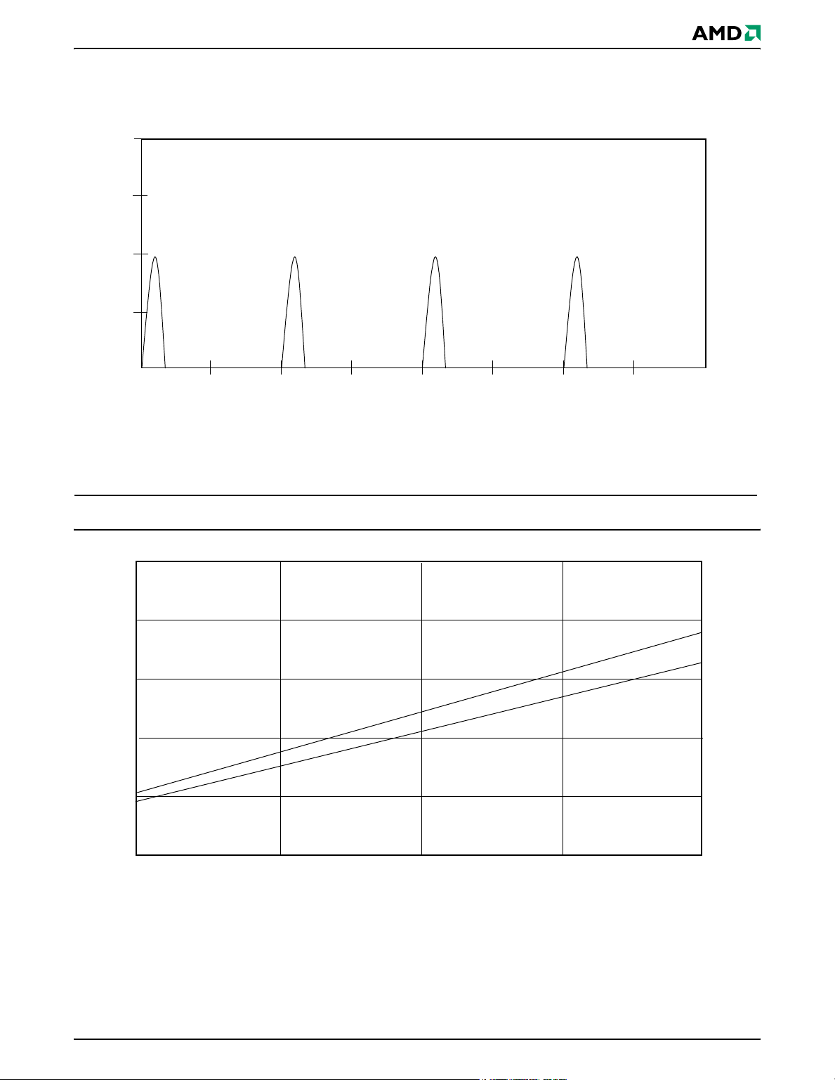
DC Characteristics (Continued)
Zero Power Flash
20
15
10
5
Supply Cur re n t in mA
0
0 500 1000 1500 2000 2500 3000 3500 4000
PRELIMINARY
Time in ns
Note: Addresses are switching at 1 MHz
Figure 1. I
Current vs. Time (Showing Active and Automatic Sleep Currents)
CC1
10
8
6
4
Supply Current in mA
2
0
12345
3.6 V
2.7 V
Frequency in MHz
Note: T = 25 °C
Figure 1. Typical I
vs. Frequency
CC1
January 21, 2005 Am29LV800D_00_A4_E Am29LV800D 29
Page 32

Te s t C o n d i t i ons
Device
Under
Test
PRELIMINARY
Table 7. Test Specifications
3.3
2.7 kΩ
C
L
6.2 kΩ
Test Condition -70
Output Load 1 TTL gate
Output Load Capacitance,
C
L
(including jig capacitance)
Input Rise and Fall Times 5 ns
Input Pulse Levels 0.0–3.0 V
30 100 pF
-90,
-120
Unit
Note: Diodes are IN3064 or
Input timing
measurement reference
levels
Figure 1. Test Setup
Output timing
measurement reference
levels
Key to Switching Waveforms
WAVEFORM INPUTS OUTPUTS
Steady
Changing from H to L
Changing from L to H
Don’t Care, Any Change Permitted Changing, State Unknown
Does Not Apply Center Line is High Impedance State (High Z)
1.5 V
1.5 V
3.0 V
0.0 V
1.5 V 1.5 V
OutputMeasurement LevelInput
Figure 1. Input Waveforms and
Measurement Levels
30 Am29LV800D Am29LV800D_00_A4_E January 21, 2005
Page 33
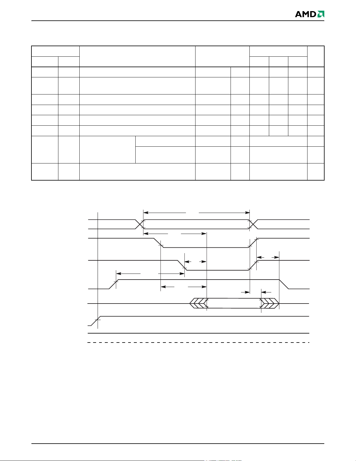
AC Characteristics
Read Operations
PRELIMINARY
Parameter
JEDEC Std Test Setup -70 -90 -120 Unit
t
AVAV
t
AVQV
t
ELQV
t
GLQV
t
EHQZ
t
GHQZ
t
Read Cycle Time (Note 1) Min 70 90 120 ns
RC
t
Address to Output Delay
ACC
t
Chip Enable to Output Delay OE# = V
CE
t
Output Enable to Output Delay Max 30 35 50 ns
OE
t
Chip Enable to Output High Z (Note 1) Max 25 30 30 ns
DF
t
Output Enable to Output High Z (Note 1) Max 25 30 30 ns
DF
Description
CE# = V
OE# = V
IL
Max 70 90 120 ns
IL
Max 70 90 120 ns
IL
Speed Options
Read Min 0 ns
Output Enable
OEH
Hold Time (Note 1)
Toggle and
Data# Polling
Output Hold Time From Addresses, CE# or
t
OH
OE#, Whichever Occurs First
(Note 1)
Min 10 ns
Min 0 ns
t
AXQX
t
Notes:
1. Not 100% tested.
2. See Figure 1 and Table 7 for test specifications.
t
RC
Addresses
Addresses Stable
t
ACC
CE#
OE#
WE#
Outputs
RESET#
RY/BY#
0 V
t
OE
t
OEH
t
CE
HIGH Z
Output Valid
Figure 1. Read Operations Timings
t
DF
t
OH
HIGH Z
January 21, 2005 Am29LV800D_00_A4_E Am29LV800D 31
Page 34
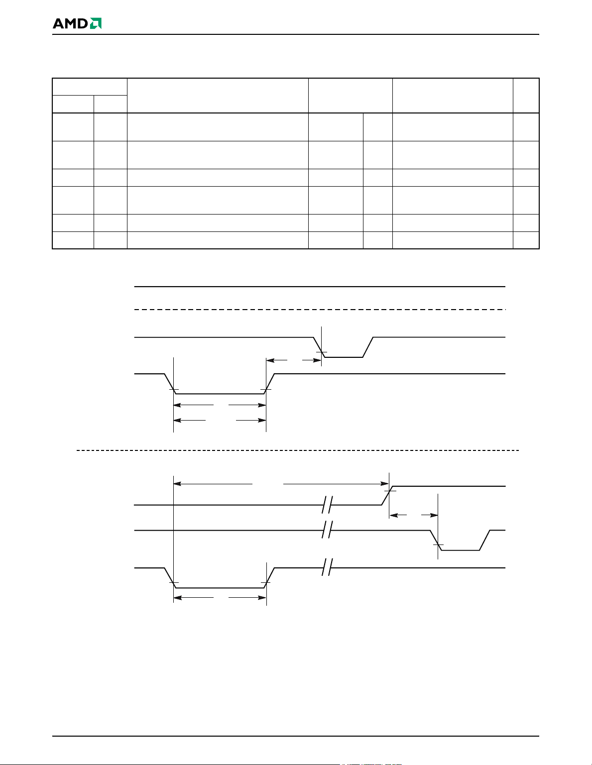
AC Characteristics
Hardware Reset (RESET#)
Parameter
PRELIMINARY
Description All Speed OptionsJEDEC Std Test Setup Unit
t
t
RESET# Pin Low (During Embedded
READY
Algorithms) to Read or Write
RESET# Pin Low (NOT During Embedded
READY
Algorithms) to Read or Write (See Note)
t
RESET# Pulse Width Min 500 ns
RP
RESET# High Time Before Read (See
t
RH
Note)
t
RESET# Low to Standby Mode Min 20 µs
RPD
t
RY/BY# Recovery Time Min 0 ns
RB
Note: Not 100% tested.
RY/BY#
CE#, OE#
RESET#
t
t
Ready
RP
(See Note)
t
RH
Max 20 µs
Max 500 ns
Min 50 ns
RY/BY#
CE#, OE#
RESET#
Reset Timings NOT during Embedded Algorithms
Reset Timings during Embedded Algorithms
t
Ready
t
RP
Figure 1. RESET# Timings
t
RB
32 Am29LV800D Am29LV800D_00_A4_E January 21, 2005
Page 35
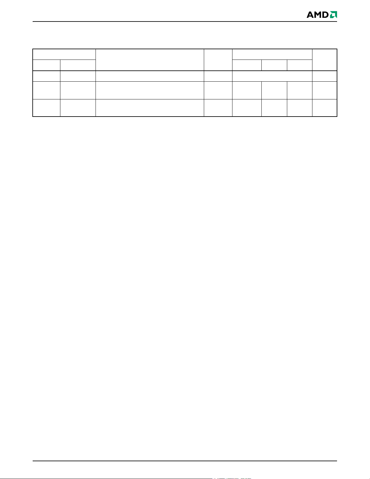
PRELIMINARY
AC Characteristics
Word/Byte Configuration (BYTE#)
Parameter Speed Options
JEDEC Std Description -70 -90 -120 Unit
t
ELFL/tELFH
t
FLQZ
t
FHQV
CE# to BYTE# Switching Low or High Max 5 ns
BYTE# Switching Low to Output HIGH
Z
BYTE# Switching High to Output
Active
Max 25 30 30 ns
Min 70 90 120 ns
January 21, 2005 Am29LV800D_00_A4_E Am29LV800D 33
Page 36
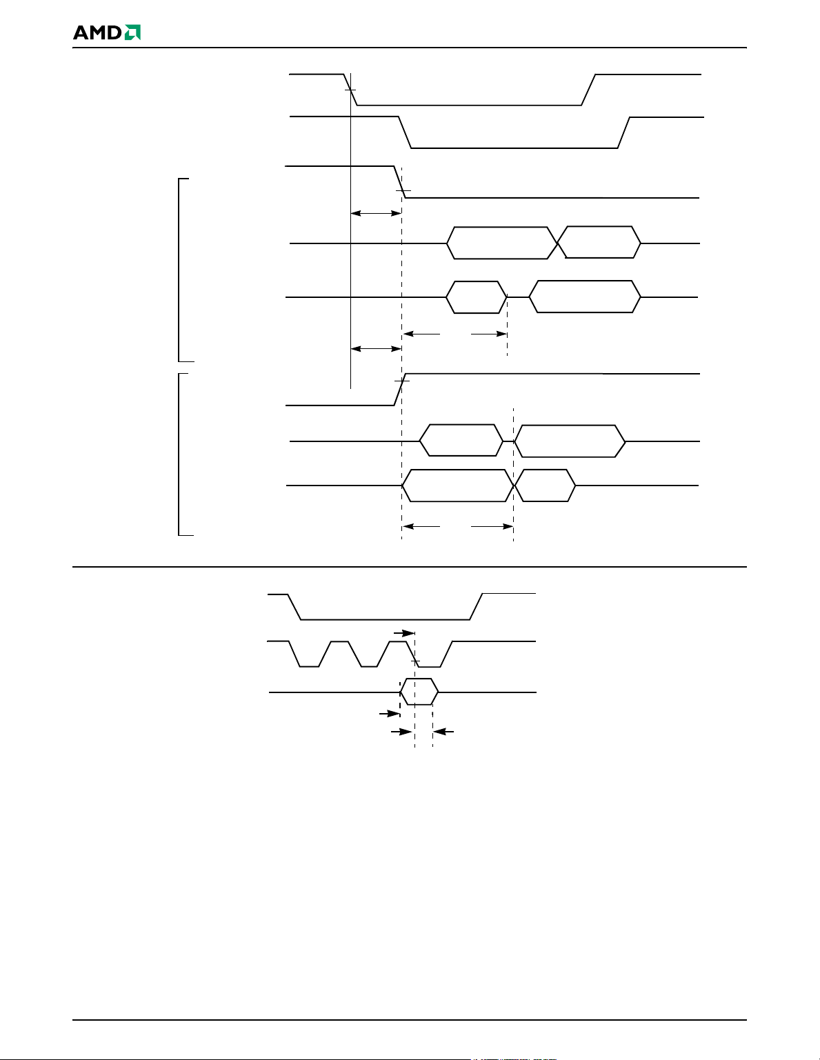
BYTE#
Switching
from word
to byte
mode
BYTE#
Switching
from byte
to word
mode
CE#
OE#
BYTE#
DQ0–DQ14
DQ15/A-1
BYTE#
DQ0–DQ14
DQ15/A-1
PRELIMINARY
t
ELFL
t
ELFH
Data Output
(DQ0–DQ14)
DQ15
Output
t
FLQ
Data
Output
Address
Input
Data
Output
Address
Input
Data Output
(DQ0–DQ14)
DQ15
Output
t
FHQ
Figure 1. BYTE# Timings for Read Operations
CE#
The falling edge of the last WE#
WE#
BYTE#
t
SET
(tAS)
t
HOLD
Note: Refer to the Erase/Program Operations table for tAS and tAH specifications.
Figure 1. BYTE# Timings for Write Operations
34 Am29LV800D Am29LV800D_00_A4_E January 21, 2005
Page 37
PRELIMINARY
AC Characteristics
Erase/Program Operations
Parameter Speed Options
JEDEC Std Description -70 -90 -120 Unit
t
AVAV
t
AVWL
t
WLAX
t
DVWH
t
WHDX
t
GHWL
t
ELWL
t
WHEH
t
WLWH
t
WHWL
t
WC
t
AS
t
AH
t
DS
t
DH
t
OES
t
GHWL
t
CS
t
CH
t
WP
t
WPH
Write Cycle Time (Note 1) Min 70 90 120 ns
Address Setup Time Min 0 ns
Address Hold Time Min 45 45 50 ns
Data Setup Time Min 35 45 50 ns
Data Hold Time Min 0 ns
Output Enable Setup Time Min 0 ns
Read Recovery Time Before Write
(OE# High to WE# Low)
Min 0 ns
CE# Setup Time Min 0 ns
CE# Hold Time Min 0 ns
Write Pulse Width Min 35 35 50 ns
Write Pulse Width High Min 30 ns
Byte Ty p 8
t
WHWH1tWHWH1
t
WHWH2tWHWH2
t
t
BUSY
Programming Operation (Note 2)
Word Typ 16
Sector Erase Operation (Note 2) Typ 1 sec
VCSVCC
t
RB
Setup Time (Note 1) Min 50 µs
Recovery Time from RY/BY# Min 0 ns
Program/Erase Valid to RY/BY# Delay Min 90 ns
Notes:
1. Not 100% tested.
2. See the “Erase and Programming Performance” section for more information.
µs
January 21, 2005 Am29LV800D_00_A4_E Am29LV800D 35
Page 38
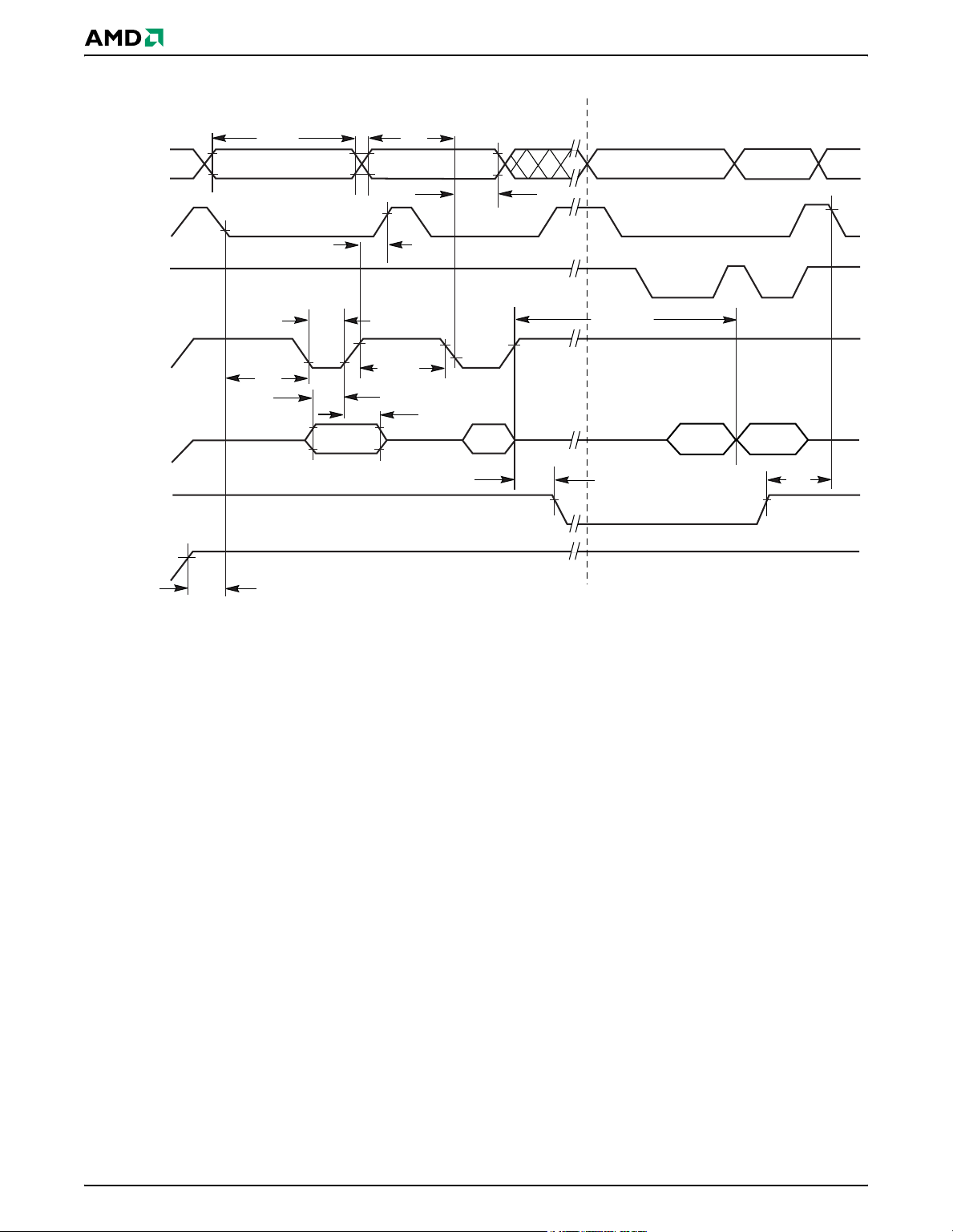
AC Characteristics
A
PRELIMINARY
ddresses
CE#
OE#
WE#
Data
RY/BY#
V
CC
t
VCS
Program Command Sequence (last two cycles)
t
WC
555h
t
CS
t
WP
t
DS
t
DH
A0h
t
AS
PA PA
t
AH
t
CH
t
WPH
PD
t
BUSY
Read Status Data (last two cycles)
PA
t
WHWH1
Status
D
OUT
t
RB
Notes:
1. PA = program address, PD = program data, D
2. Illustration shows device in word mode.
is the true data at the program address.
OUT
Figure 1. Program Operation Timings
36 Am29LV800D Am29LV800D_00_A4_E January 21, 2005
Page 39

AC Characteristics
PRELIMINARY
Erase Command Sequence (last two cycles) Read Status Data
Addresses
CE#
OE#
WE#
Data
RY/BY#
V
CC
t
VCS
t
WC
2AAh SA
555h for chip erase
t
CH
t
WP
t
t
CS
t
DS
t
WPH
DH
55h
t
AS
t
AH
30h
10 for Chip Erase
t
BUSY
t
WHWH2
VA
In
Progress
VA
Complete
t
RB
Notes:
1. SA = sector address (for Sector Erase), VA = Valid Address for reading status data (see “Write Operation
Status”).
2. Illustration shows device in word mode.
Figure 1. Chip/Sector Erase Operation Timings
January 21, 2005 Am29LV800D_00_A4_E Am29LV800D 37
Page 40
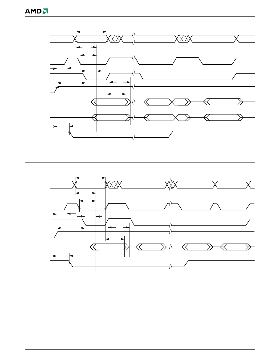
AC Characteristics
Z
Z
A
d
ddresses
CE#
t
CH
OE#
t
OEH
WE#
DQ7
t
ACC
PRELIMINARY
t
RC
VA
t
CE
t
OE
t
DF
t
OH
Complement
VA VA
Complement
True
Valid Data
High
DQ0–DQ6
t
BUSY
Status Data
Status Data
True
Valid Data
High
RY/BY#
Note: VA = Valid address. Illustration shows firs t status cycl e after comma nd seque nce, last status read cycle, a nd array data
read cycle.
Figure 1. Data# Polling Timings (During Embedded Algorithms)
t
RC
Addresses
CE#
t
CH
OE#
t
OEH
WE#
DQ6/DQ2
t
RY/BY#
BUSY
High Z
t
ACC
VA
t
CE
t
OE
t
DF
t
OH
(first read) (second read) (stops toggling)
VA VA
Valid Status
VA
Valid DataValid StatusValid Status
Note: VA = V alid address; not required for DQ6. Illustration shows first two status cycle after command sequence, last status rea
cycle, and array data read cycle.
Figure 1. Toggle Bit Timings (During Embedded Algorithms)
38 Am29LV800D Am29LV800D_00_A4_E January 21, 2005
Page 41

PRELIMINARY
n
AC Characteristics
Enter
Embedded
Erasing
WE#
DQ6
DQ2
Note: The system may use CE# or OE# to toggle DQ2 and DQ6. DQ2 toggles only when read at an address within a
erase-suspended sector.
Erase
Erase
Suspend
Erase Suspend
Enter Erase
Suspend Program
Erase
Read
Suspend
Program
Figure 1. DQ2 vs. DQ6
Erase Suspend
Read
Erase
Resume
Erase
Erase
Complete
Temporary Sector Unprotect
Parameter
All Speed OptionsJEDEC Std Description Unit
t
VIDR VID
RESET# Setup Time for Temporary
t
RSP
Sector Unprotect
Note: Not 100% tested.
12 V
RESET#
0 or 3 V
CE#
WE#
RY/BY#
Rise and Fall Time (See Note) Min 500 ns
Min 4 µs
0 or 3 V
t
VIDR
t
VIDR
Program or Erase Command Sequence
t
RSP
Figure 1. Temporary Sector Unprotect
Timing Diagram
January 21, 2005 Am29LV800D_00_A4_E Am29LV800D 39
Page 42

AC Characteristics
R
V
ID
V
ESET#
IH
PRELIMINARY
SA, A6,
A1, A0
Valid* Valid* Valid*
Sector Protect/Unprotect Verify
Data
60h 60h 40h
1 µs
Sector Protect: 150 µs
Sector Unprotect: 15 ms
CE#
WE#
OE#
* For sector protect, A6 = 0, A1 = 1, A0 = 0. For sector unprotect, A6 = 1, A1 = 1, A0 = 0.
Figure 1. Sector Protect/Unprotect
Timing Diagram
Status
40 Am29LV800D Am29LV800D_00_A4_E January 21, 2005
Page 43
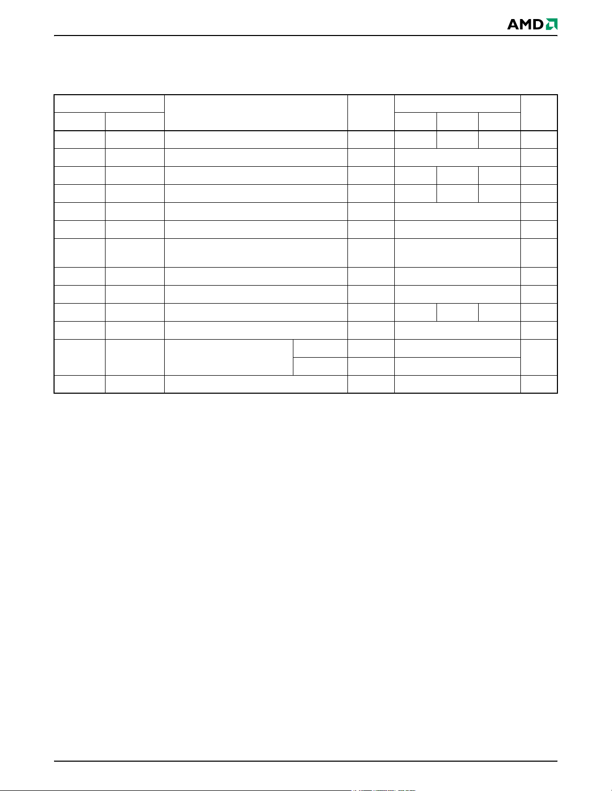
PRELIMINARY
AC Characteristics
Alternate CE# Controlled Erase/Program Operations
Parameter Speed Options
JEDEC Std Description -70 -90 -120 Unit
t
AVAV
t
AVEL
t
ELAX
t
DVEH
t
EHDX
t
GHEL
t
WLEL
t
EHWH
t
ELEH
t
EHEL
t
WHWH1
t
WHWH2
t
WC
t
AS
t
AH
t
DS
t
DH
t
OES
t
GHEL
t
WS
t
WH
t
CP
t
CPH
t
WHWH1
t
WHWH2
Write Cycle Time (Note 1) Min 70 90 120 ns
Address Setup Time Min 0 ns
Address Hold Time Min 45 45 50 ns
Data Setup Time Min 35 45 50 ns
Data Hold Time Min 0 ns
Output Enable Setup Time Min 0 ns
Read Recovery Time Before Write
(OE# High to WE# Low)
WE# Setup Time Min 0 ns
WE# Hold Time Min 0 ns
CE# Pulse Width Min 35 35 50 ns
CE# Pulse Width High Min 30 ns
Programming Operation
(Note 2)
Sector Erase Operation (Note 2) Typ 1 sec
Notes:
1. Not 100% tested.
2. See the “Erase and Programming Performance”
section for more information.
Min 0 ns
Byte Ty p 8
µs
Word Typ 16
January 21, 2005 Am29LV800D_00_A4_E Am29LV800D 41
Page 44
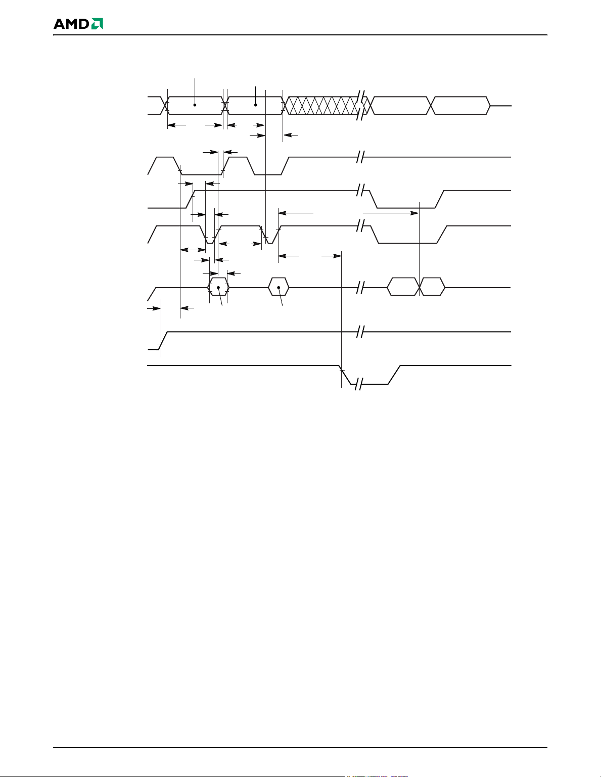
AC Characteristics
555 for program
2AA for erase
PRELIMINARY
PA for program
SA for sector erase
555 for chip erase
Data# Polling
Addresses
WE#
OE#
CE#
Data
RESET#
RY/BY#
PA
t
WC
t
WH
t
WS
t
RH
t
AS
t
GHEL
t
CP
t
CPH
t
DS
t
DH
A0 for program
55 for erase
t
AH
t
BUSY
PD for program
30 for sector erase
10 for chip erase
t
WHWH1 or 2
DQ7# D
OUT
Notes:
1. PA = program address, PD = program data, DQ7# = complement of the data written to the device, D
data written to the device.
2. Figure indicates the last two bus cycles of command
sequence.
3. Word mode address used as an example.
Figure 1. Alternate CE# Controlled Write Operation Timings
OUT
=
42 Am29LV800D Am29LV800D_00_A4_E January 21, 2005
Page 45

PRELIMINARY
Erase and Programming Performance
Typ (Note
Parameter
1) Max (Note 2) Unit Comments
Sector Erase Time 1 10 s
Chip Erase Time 14 s
Byte Programming Time 8 300 µs
Word Programming Time 16 360 µs
Chip Programming
Time
(Note 3)
Notes:
1. Typical program and erase times assume the following conditions: 25°C, 3.0 V VCC, 1,000,000 cycles.
Additionally, programming typicals assume checkerboard pattern.
2. Under worst case conditions of 90°C, VCC = 2.7 V, 1,000,000 cycles.
3. The typical chip programming time is considerably less than the maximum chip programming time listed, s ince most
bytes program faster than the maximum program times listed.
4. In the pre-programming step of the Embedded Erase algorithm, all bytes are programmed to 00h before erasure.
5. System-level overhead is the time required to execute the two- or four-bus-cycle sequence for the program
command. See Table 5 for further information on command definitions .
6. The device has a guaranteed minimum erase and program cycle endurance of 1,000,000 cycles.
Byte Mode 8.4 25 s
Word M ode 5.8 17 s
Excludes 00h programming
prior to erasure
Excludes system level
overhead
(Note 5)
Latchup Characteristics
Description Min Max
Input voltage with respect to VSS on all pins except I/O pins
(including A9, OE#, and RESET#)
–1.0 V 12.5 V
Input voltage with respect to VSS on all I/O pins –1.0 V VCC + 1.0 V
VCC Current –100 mA +100 mA
Includes all pins except VCC. Test conditions: VCC =
3.0 V, one pin at a time.
TSOP and SO Pin Capacitance
Parameter
Symbol Parameter Description Test Setup Typ Max Unit
C
IN
C
OUT
C
IN2
Notes:
1. Sampled, not 100% tested.
2. Test conditions TA = 25°C, f = 1.0 MHz.
Input Capacitance VIN = 0 6 7.5 pF
Output Capacitance V
Control Pin Capacitance VIN = 0 7.5 9 pF
= 0 8.5 12 pF
OUT
Data Retention
Test
Parameter
Minimum Pattern Data Retention Time
Conditions
150°C 10 Yea rs
125°C 20 Yea rs
Min Unit
43 Am29LV800D Am29LV800D_00_A4_E January 21, 2005
Page 46

Physical Dimensions*
TS 048—48-Pin Standard TSOP
PRELIMINARY
* For reference only. BSC is an ANSI standard for Basic Space Centering.
Dwg rev AA; 10/99
January 21, 2005 Am29LV800D_00_A4_E Am29LV800D 44
Page 47

Physical Dimensions
TSR048—48-Pin Reverse TSOP
PRELIMINARY
* For reference only. BSC is an ANSI standard for
Basic Space Centering.
Dwg rev AA; 10/99
45 Am29LV800D Am29LV800D_00_A4_E January 21, 2005
Page 48

PRELIMINARY
Physical Dimensions
FBB 048—48-Ball Fine-Pitch Ball Grid Array (FBGA) 6 x 9 mm
Dwg rev AF; 10/99
January 21, 2005 Am29LV800D_00_A4_E Am29LV800D 46
Page 49
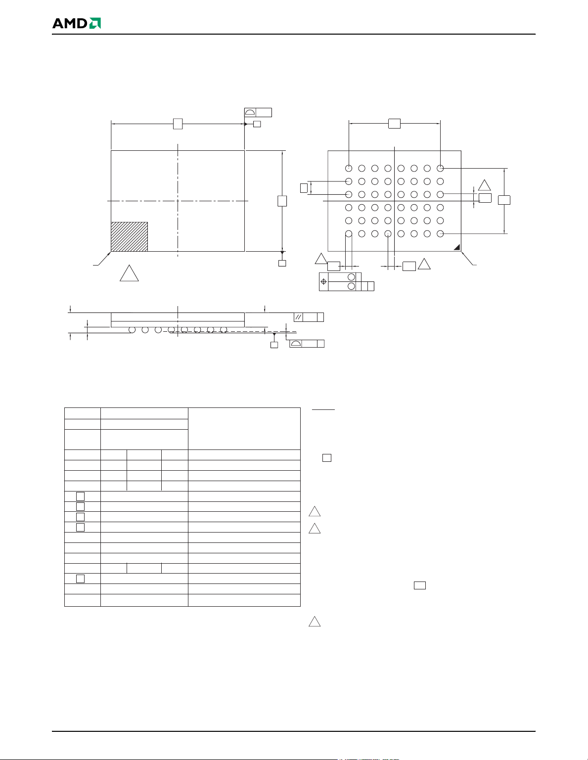
PRELIMINARY
Physical Dimensions
VBK 048 - 48 Ball Fine-Pitch Ball Grid Array (FBGA) 6.15 x 8.15 mm
0.10
(4X)
D
A
e
E
H
D1
6
5
4
3
2
1
BCDEFG
A
SE
7
E1
PIN A1
CORNER
INDEX MARK
10
B
TOP VIEW
A
A1
SEATING PLANE
A2
C
SIDE VIEW
PACKAGE VBK 048
JEDEC N/A
6.15 mm x 8.15 mm NOM
PACKAGE
SYMBOL MIN NOM MAX NOTE
A --- --- 1.00 OVERALL THICKNESS
A1 0.18 --- --- BALL HEIGHT
A2 0.62 --- 0.76 BODY THICKNESS
D 8.15 BSC. BODY SIZE
E 6.15 BSC. BODY SIZE
D1 5.60 BSC. BALL FOOTPRINT
E1 4.00 BSC. BALL FOOTPRINT
MD 8 ROW MATRIX SIZE D DIRECTION
ME 6 ROW MATRIX SIZE E DIRECTION
N 48 TOTAL BALL COUNT
fb 0.33 --- 0.43 BALL DIAMETER
e 0.80 BSC. BALL PITCH
SD / SE 0.40 BSC. SOLDER BALL PLACEMENT
--- DEPOPULATED SOLDER BALLS
6
fb
M
f 0.08
C
M
f 0.15
BA
C
SD
7
A1 CORNER
BOTTOM VIEW
C0.10
C0.08
NOTES:
1. DIMENSIONING AND TOLERANCING PER ASME Y14.5M-1994.
2. ALL DIMENSIONS ARE IN MILLIMETERS.
3. BALL POSITION DESIGNATION PER JESD 95-1, SPP-010 (EXCEPT
AS NOTED).
4. e REPRESENTS THE SOLDER BALL GRID PITCH.
5. SYMBOL "MD" IS THE BALL ROW MATRIX SIZE IN THE
"D" DIRECTION.
SYMBOL "ME" IS THE BALL COLUMN MATRIX SIZE IN THE
"E" DIRECTION.
N IS THE TOTAL NUMBER OF SOLDER BALLS.
6 DIMENSION "b" IS MEASURED AT THE MAXIMUM BALL
DIAMETER IN A PLANE PARALLEL TO DATUM C.
7 SD AND SE ARE MEASURED WITH RESPECT TO DATUMS
A AND B AND DEFINE THE POSITION OF THE CENTER
SOLDER BALL IN THE OUTER ROW.
WHEN THERE IS AN ODD NUMBER OF SOLDER BALLS IN
THE OUTER ROW PARALLEL TO THE D OR E DIMENSION,
RESPECTIVELY, SD OR SE = 0.000.
WHEN THERE IS AN EVEN NUMBER OF SOLDER BALLS IN
THE OUTER ROW, SD OR SE = e/2
8. NOT USED.
9. "+" INDICATES THE THEORETICAL CENTER OF DEPOPULATED
BALLS.
10 A1 CORNER TO BE IDENTIFIED BY CHAMFER, LASER OR INK
MARK, METALLIZED MARK INDENTATION OR OTHER MEANS.
3338 \ 16-038.25b
47 Am29LV800D Am29LV800D_00_A4_E January 21, 2005
Page 50

PRELIMINARY
Physical Dimensions
SO 044—44-Pin Small Outline Package
Dwg rev AC; 10/99
January 21, 2005 Am29LV800D_00_A4_E Am29LV800D 48
Page 51

PRELIMINARY
Revision Summary
Revision A (January 19, 2004)
Changed data sheet status to Advance Information to indicate new 0.23 µm process technology. The base device part number has
changed from Am29LV800B to Am29LV800D.
Specifications for I
CC1
, t
WHWH1
changed. Extended temperature is no longer
available. All other specifications in the data
sheet remain unchanged. Deleted references to
KGD option in Connection Diagrams section.
(This document was formerly released as publication 21490, revision H.)
Revision A+1 (February 3, 2004)
Distinctive Characteristics, General Description, Ordering Information
Deleted references to KGD option. (This document was formerly released as publication
21490, revision H1.)
Revision A+2 (April 2, 2004)
General Description
Removed unlock bypass section.
, t
WHWH2
have
Global
Converted datasheet to Preliminary.
Ordering Information
Added Pb-Free packages and updated Valid
Combinations tables to include changes.
Absolute Maximum Rating
Changed ambient with power applied from
125°C to 85°C.
Revision A+3 (June 23, 2004)
Global change
Changed all Helvetica/Times Roman fonts to Gill
Sans For AMD or Verdana.
“Physical Dimensions” on page 47
Added VBK048 Package Drawing.
“Ordering Information” on page 8
Added “WC =...” to Standard Products table.
Added “WCC, WCI, WCD, WCF” to Valid combinations table.
Added Colophon.
Revision A+4 (January 21, 2005)
Added migration statement.
Colophon
The products described in this document are designed, developed and manufactured as contemplated for general use, including without limitation, ordinary industrial use, general office use, personal use, and household use, but are not designed, developed and manufactured as contemplated (1) for any use that includes fatal risks or dangers that, unless extremely high safety is secured, could have a serious effect to the
public, and could lead directly to death, personal injury, severe physical damage or other loss (i.e., nuclear reaction control in nuclear facility,
aircraft flight control, air traffic control, mass transport control, medical life support system, missile launch control in weapon system), or (2) for
any use where chance of failure is intolerable (i.e., submersible repeater and artificial satellite). Please note that FASL will not be liable to you
and/or any third party for any claims or damages arising in connection with above-mentioned uses of the products. Any semiconductor devices
have an inherent chance of failure. You must protect against injury, damage or loss from such failures by incorporating safety design measures
into your facility and equipment such as redundancy, fire protection, and prevention of over-current levels and other abnormal operatin g condi
tions. If any products described in this document represent goods or technologies subject to cert ai n res tr icti ons on export under the Foreign Exchange and Foreign Trade Law of Japan, the US Export Administration Regulations or the applicable laws of any other country, the prior
authorization by the respective government entity will be required for export of those products.
Trademarks
Copyright © 2000–2005 Advanced Micro Devices, Inc. All rights reserved.
AMD, the AMD logo, and combinations thereof are registered trademarks of Advanced Micro Devices, Inc.
ExpressFlash is a trademark of Advanced Micro Devices, Inc.
Product names used in this publication are for identification purposes only and may be trademarks of their respective companies.
49 Am29LV800D Am29LV800D_00_A4_E January 21, 2005
-
Page 52

WWW.ALLDATASHEET.COM
Copyright © Each Manufacturing Company.
All Datasheets cannot be modified without permission.
This datasheet has been download from :
www.AllDataSheet.com
100% Free DataSheet Search Site.
Free Download.
No Register.
Fast Search System.
www.AllDataSheet.com
 Loading...