

Page 1

Am29LV640D/Am29LV641D
Data Sheet
July 2003
The following document specifies Spansion memory products that are now offered by both Advanced
Micro Devices and Fujitsu. Although the docu ment is ma rked with the name o f the comp any that o riginally developed the specification, these products will be offered to customers of both AMD and
Fujitsu.
Continuity of Specifications
There is no change to this datasheet as a result of offering the device as a Spansion product. Any
changes that have been made are the result of normal datasheet improvement and are noted in the
document revision summary, where supported. Future routine revisions will occur when appropriate,
and changes will be noted in a revision summary.
Continuity of Ordering Part Numbers
AMD and Fujitsu continue to support existing part numbers beginning with “Am” and “MBM”. To order
these products, please use only the Ordering Part Numbers listed in this document.
For More Information
Please contact your local AMD or Fujitsu sales office for additional information about Spansion
memory solutions.
Publication Number 22366 Revision B Amendment +8 Issue Date September 20, 2002
Page 2

Am29LV640D/Am29LV641D
64 Megabit (4 M x 16-Bit) CMOS 3.0 Volt-only
Uniform Sector Flash Memory with VersatileIO Control
DISTINCTIVE CHARACTERISTICS
■ Single power supply operation
— 3.0 to 3.6 volt read, erase, and program operations
■ VersatileIO contro l
— Device generates output voltages and tolerates data
input voltages on the DQ input/ouputs as determined
by the voltage on V
■ High performance
— Access times as fast as 90 ns
■ Manufactured on 0.23 µm process technology
■ CFI (Common Flash Interface) compliant
— Provides device-specific information to the system,
allowing host software to easily reconfigure for
different Flash devices
■ SecSi (Secured Silicon) Sector region
— 128-word sector for permanent, secure identification
through an 8-word random Elec tron ic Ser ial Num be r
— May be programmed and locked at the factory or by
the customer
— Accessible through a comma nd seque nce
■ Ultra low power consumption (typical values at 3.0 V ,
5 MHz)
— 9 mA typical active read current
— 26 mA typical erase/program current
— 200 nA typical standby mode current
■ Flexible sector architecture
— One hundred twenty-eight 32 Kword sectors
■ Sector Protection
— A hardware method to lock a sector to prevent
program or erase operations within that sector
— Sectors can be locked in-system or via programming
equipment
— Temporary Sector Unprotect feature allows code
changes in previously locked sectors
■ Embedded Algorithms
— Embedded Erase algorith m aut oma tic ally
preprograms and erases the entire chip or any
combination of designated sectors
— Embedded Program algorithm automatically writes
and verifies data at specified addresses
IO
■ Compatibility with JEDEC standards
— Pinout and software compatible with single-power
supply Flash
— Superior inadvertent write protection
■ Minimum 1 million erase cycle guarantee per sector
■ Package options
— 48-pin TSOP (Am29LV641DH/DL only)
— 56-pin SSOP (Am29LV640DH/DL only)
— 63-ball Fine-Pitch BGA (Am29LV640DU only)
— 64-ball Fortified BGA (Am29LV640DU only)
■ Erase Suspend/Erase Resume
— Suspends an erase operation to read data from, or
program data to, a sect27
— or that is not being erased, then resumes the erase
operation
■ Data# Polling and toggle bits
— Provides a software method of detecting program or
erase operation completion
■ Unlock Bypass Program command
— Reduces overall programming time when issuing
multiple program command sequences
■ Ready/Busy# pin (RY/BY#) (Am29LV640DU in FBGA
package only)
— Provides a hardware method of detecting program or
erase cycle completion
■ Hardware reset pin (RESET#)
— Hardware method to reset the device for reading array
data
■ WP# pin (Am29LV641DH/DL in TSOP,
Am29LV640DH/DL in SSOP only)
— At V
— At V
— An internal pull up to V
■ ACC pin
— Accelerates programming time for higher throughput
■ Program and Erase Performance (V
the ACC input pin)
— Word program time: 11 µs typical
— Sector erase time: 0.9 s typical for each 32 Kword
, protects the first or last 32 Kword sector,
IL
regardless of sector protect/unprotect status
, allows removal of sector protection
IH
during system production
sector
is provided
CC
not applied to
HH
Publication# 22366 Rev: B Amendment/+8
Issue Date: September 20, 2002
Refer to AMD’s Website (www.amd.com) for the latest information.
Page 3

GENERAL DESCRIPTION
The Am29LV640DU/Am29LV641DU is a 64 Mbit, 3.0
Volt (3.0 V to 3.6 V) single power supply flash memory
devices organized as 4 ,194,304 wo rds. Data appe ars
on DQ0-DQ15. The device is designed to be programmed in-system with the stand ard system 3.0 volt
supply. A 12.0 volt VPP is not required for program
V
CC
or erase operations. The device can also be programmed in standard EPROM programmers.
Access times of 90 and 120 ns are available for applications where V
ns are available for applications where V
device is offered in 48- pin TSOP, 56-pin SSOP, 63-ball
Fine-Pitch BGA and 64-ball Fortified BGA packages.
To eliminate bus contention each device has separate
chip enable (CE#), write enable (WE#) and output enable (OE#) controls.
Each device requires only a single 3.0 Volt power
supply (3.0 V to 3.6 V) for both read and write functions. Internally generated and regula ted voltages ar e
provided for the program and erase operations.
The device is entirely command set compatible with
the JEDEC single-pow er-supply Flash standard.
Commands are written to the command register using
standard microprocessor write timing. Register contents serve as inputs to an internal state-machine that
controls the erase and programming circuitry. Write
cycles also internally latch addresses and data
needed for the programming and erase operations.
Reading data out of the device is similar to reading
from other Flash or EPROM devices.
≥ VCC. Access times of 100 and 120
IO
< VCC. The
IO
gle) status bits. After a program or erase cycle has
been completed, the device is ready to read array data
or accept another command.
The sector erase archite cture allow s memo ry sectors to be erased and reprogrammed without affecting
the data conten ts of oth er sec tors. Th e devi ce is fully
erased when shipped from the factory.
Hardware data protection measures include a low
detector that automatically inhibits write opera-
V
CC
tions during power transitions. The hardware sector
protection feature disables both program and erase
operations in any combination of sectors of memory.
This can be achieved in-system or via programming
equipment.
The Erase Suspen d/Erase R esume fe ature ena bles
the user to put erase on hold for any period of time to
read data from, or prog ram data to, an y sector that is
not selected for erasure. True background erase can
thus be achieved.
The hardware RESET# p in terminates any opera tion
in progress and re sets the internal state machine to
reading array data. The RESET# pin may be tied to
the system reset circuitry. A system reset would thus
also reset the device, enabling the system microprocessor to read boot-up firmware from the Flash mem ory device.
The device offers a standby mode as a power-saving
feature. Once the system p laces the device into th e
standby mode power consumption is greatly reduced.
Device programming occurs by executing the program
command sequence. This initiates the Embedded
Program algorithm—an internal algorithm that auto-
matically times the program pulse widths and verifies
proper cell margin. The Unlock Bypass mode facilitates faster programming times by requiring only two
write cycles to program data instead of four.
Device erasure occurs by executing the erase command sequence. This initiates the Embedded Erase
algorithm—an internal algorithm that automatically
preprograms the array (if it is not alread y programmed) before executin g the erase op eration. During erase, the device automatically times the erase
pulse widths and verifies proper cell margin.
The VersatileIO™ (V
) control allows the host system
IO
to set the voltage levels that the device generates and
tolerates on CE# and DQ I/O s to the same voltag e
level that is asserted on V
. VIO is available in two
IO
configurations (1.8–2.9 V and 3.0–5.0 V) for operation
in various system environments.
The host system can detect whether a program or
erase operation is complete by observing the RY/BY#
pin, by reading the DQ7 (Data# Polling), or DQ6 (tog-
The SecSi (Secured Silicon) Sector provid es an
minimum 128-word area for code or data that can be
permanently protected. Once this sector is protected,
no further programming or erasing within the sector
can occur.
The Write Protect (WP#) feature prot ects the f irst o r
last sector by asserting a logic low on the WP# pin.
The protected sector will still be protected even during
accelerated programming.
The accelerated program (ACC) feature allows the
system to program the device at a much faster rate.
When ACC is pulled high to V
, the device enters the
HH
Unlock Bypass mode, enabling the user to reduce the
time needed to do the program operation. This feature
is intended to increas e factory th roughput d uring sys tem production, but may also be used in the field if desired.
AMD’s Flash techn ology combines y ears of Flash
memory manufacturing experience to produce the
highest levels of quality, reliability and cost effectiveness. The device electrically erases all bits within a
sector simultaneously via Fowler-Nordheim tunnelling.
The data is programmed using hot electron injection.
2 Am29LV640D/Am29LV641D September 20, 2002
Page 4

TABLE OF CONTENTS
Product Selector Guide . . . . . . . . . . . . . . . . . . . . . 4
Block Diag ra m . . . . . . . . . . . . . . . . . . . . . . . . . . . . 4
Connection Diagrams . . . . . . . . . . . . . . . . . . . . . . . 5
Special Handling Instructions for FBGA/fBGA Packages .........8
Pin Description . . . . . . . . . . . . . . . . . . . . . . . . . . . . 9
Logic Symbol . . . . . . . . . . . . . . . . . . . . . . . . . . . . . 9
Ordering Information . . . . . . . . . . . . . . . . . . . . . .10
Device Bus Operations . . . . . . . . . . . . . . . . . . . . .11
Table 1. Device Bus Operations .............. .............. .........................11
VersatileIO (VIO) Control .......... .. ........................ .. ... ............11
Requirements for Reading Array Data ...................... .. ...........11
Writing Commands/Command Sequences ..................... .......12
Accelerated Program Operation ......................................................12
Autoselect Function s ......................... .............. ........................... .....12
Standby Mode ................................... .....................................12
Automatic Sleep Mode ...........................................................12
RESET#: Hardware Reset Pin ...............................................12
Output Disable Mode ..............................................................13
Table 2. Sector Address Table ............... ........................... ..............13
Autoselect Mode ........ ....................... .................... ..................17
Table 3. Autoselect Codes, (High Voltage Method) ..................... ..17
Sector Group Protection and Unprotection ...................... .......18
Table 4. Sector Group Protection/Unprotection Address Table .....18
Write Protect (WP#) ................................................................19
Temporary Sector Group Unprotect .......................................19
Figure 1. Temporary Sector Group Unprotect Operation................ 19
Figure 2. In-System Sector Group Protect/Unprotect Algorithms ... 20
SecSi (Secured Silicon) Sector Flash Memory Region ..........21
Table 5. SecSi Sector Contents ......................................................21
Hardware Data Protection ......................................................21
Low VCC Write Inhibit .....................................................................21
Write Pulse “Glitch” Protection ................................................. .......22
Logical Inhibit ............................................... ................ ......... ..........2 2
Power-Up Write Inhibit ............................................... .....................22
Common Flash Memory Interface (CFI). . . . . . . 22
Table 6. CFI Query Identification String .......................................... 22
System Interface String...................... .............. ........................... .... 23
Table 8. Device Geometry Definit ion.............................................. 23
Table 9. Primary Vendor-Specific Extended Query........................ 24
Command Definitions . . . . . . . . . . . . . . . . . . . . . 24
Reading Array Data ................................................................24
Reset Command ......................................... ............................25
Autoselect Command Sequence ............................................25
Enter SecSi Sector/Exit SecSi Sector CommandSequence ..25
Word Program Command Sequence .....................................25
Unlock Bypass Command Sequence ..............................................26
Figure 3. Program Operation........... .............. ............. .................... 26
Chip Erase Command Sequence ...........................................26
Sector Erase Command Sequence ........................................27
Erase Suspend/Erase Resume Commands ...........................27
Figure 4. Erase Operation............................................................... 28
Command Definitions .............................................................29
Command Definitions...................................................................... 29
Write Operation Status . . . . . . . . . . . . . . . . . . . . .30
DQ7: Data# P o ll in g .......... .. ........................ ........................ .....30
Figure 5. Data# Polling Algorithm................................................... 30
RY/BY#: Ready/Busy# ............................................................31
DQ6: Toggle Bit I ....................................................................31
Figure 6. Toggle Bit Algorithm........................................................ 31
DQ2: Toggle Bit II ...................................................................32
Reading Toggle Bits DQ6/DQ2 ...............................................32
DQ5: Exceeded Timing Limits ................................................32
DQ3: Sector Era s e Time r ..... ........................ .. ........................32
Table 11. Write Operation Sta tus ........................ .............. .............33
Absolute Maximum Ratings . . . . . . . . . . . . . . . . 34
Figure 7. Maximum Negative Overshoot Waveform ..................... 34
Figure 8. Maximum Positive Overshoot Waveform....................... 34
Operating Ranges . . . . . . . . . . . . . . . . . . . . . . . . 34
DC Characteristics . . . . . . . . . . . . . . . . . . . . . . . . 35
Figure 9. I
Activeand Automatic Sleep Currents)............... .............. .............. 36
Figure 10. Typical I
Current vs. Time (Showing
CC1
vs. Frequency.................. .......................... 36
CC1
Test Conditions . . . . . . . . . . . . . . . . . . . . . . . . . . 37
Figure 11. Test Setup................... .............. .............. ..................... 37
Table 12. Test Specifications ................................... ......................37
Key to Switching Waveforms. . . . . . . . . . . . . . . . 37
Figure 12. Input Waveforms and
Measurement Levels...................................................................... 37
AC Characteristics . . . . . . . . . . . . . . . . . . . . . . . . 38
Read-Only Operations ...........................................................38
Figure 13. Read Operation Timings............................................... 38
Hardware Reset (RESET#) .............................................. ......39
Figure 14. Reset Timings............................................................... 39
Erase and Program Operations ........... .. .................................40
Figure 15. Program Operation Timings.......................................... 41
Figure 16. Accelerated Program Timing Diagram.......................... 41
Figure 17. Chip/Sector Erase Operation Timings.......................... 42
Figure 18. Data# Polling Timings
(During Embedded Algorithms)...................................................... 43
Figure 19. Toggle Bit Timings
(During Embedded Algorithms)...................................................... 44
Figure 20. DQ2 vs. DQ6......................... ............................ ............ 44
Temporary Sector Unprotect .................................................. 45
Figure 21. Temporary Sector Group Unprotect Timing Diagram... 45
Figure 22. Sector Group Protect and Unprotect Timing Diagram.. 46
Alternate CE# Controlled Erase and Program Operations .....47
Figure 23. Alternate CE# Controlled Write
(Erase/Program)Operation Timings.................. ........................... . 48
Erase And Programming Performance . . . . . . . 49
Latchup Characteristics. . . . . . . . . . . . . . . . . . . . 49
TSOP Pin Capacitance. . . . . . . . . . . . . . . . . . . . . 49
Data Retention. . . . . . . . . . . . . . . . . . . . . . . . . . . . 49
Physical Dimensions . . . . . . . . . . . . . . . . . . . . . . 50
SSO056—56-Pin Shrink Small Outline Package (SSOP) ......50
FBE063—63-Ball Fine-Pitch Ball Grid Array
(FBGA) 12 x 11 mm package ................................................. 51
LAA064—64-Ball Fortified Ball Grid Array
(FBGA) 13 x 11 mm package ................................................. 52
TS 048—48-Pin Standard TSOP ............................................53
TSR048—48-Pin Reverse TSOP ............................ ... ............54
Revision Summary . . . . . . . . . . . . . . . . . . . . . . . . 55
September 20, 2002 Am29LV640D/Am29LV641D 3
Page 5
PRODUCT SELECTOR GUIDE
Part Number Am29LV640D/Am29LV641D
= 3.0–3.6 V, VIO = 3.0–5.0 V 90R 120R
V
Speed Option
CC
V
= 3.0–3.6 V, VIO = 1.8–2.9 V 101R 121R
CC
Max Access Time (ns) 90 100 120
CE# Access Time (ns) 90 100 120
OE# Access Time (ns) 35 35 50
Note: See “AC Characteristics” for full specifications.
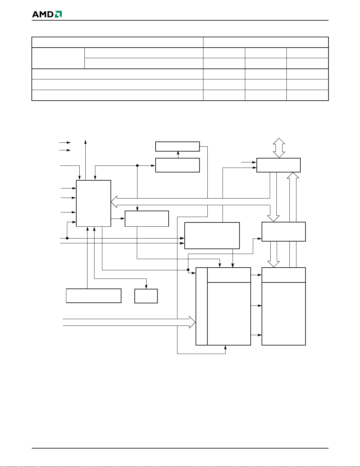
BLOCK DIAGRAM
DQ0
–DQ15
Input/Output
Buffers
V
CC
V
SS
RESET#
RY/BY# (Note 1)
Sector Switches
Erase Voltage
Generator
V
IO
WE#
WP#
State
Control
(Note 2)
ACC
Command
Register
PGM Voltage
Generator
CE#
OE#
VCC Detector
Timer
A0–A21
Notes:
1. RY/BY# is only available in the FBGA package.
2. WP# is only available in the TSOP and SSOP packages.
Chip Enable
Output Enable
STB
Logic
Address Latch
Y-Decoder
X-Decoder
STB
Data
Latch
Y-Gating
Cell Matrix
4 Am29LV640D/Am29LV641D September 20, 2002
Page 6
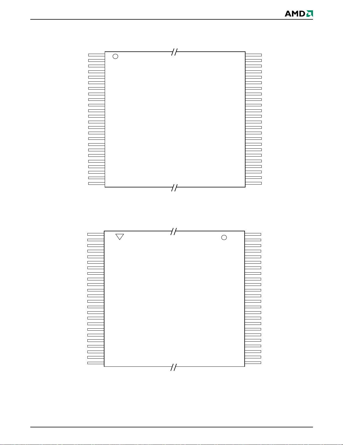
CONNECTION DIAGRAMS
A15
A14
A13
A12
A11
A10
A9
A8
A21
A20
WE#
RESET#
ACC
WP#
A19
A18
A17
A7
A6
A5
A4
A3
A2
A1
1
2
3
4
5
6
7
8
9
10
11
12
13
14
15
16
17
18
19
20
21
22
23
24
48-Pin Standard TSOP
(Am29LV641DH/DL only)
48
47
46
45
44
43
42
41
40
39
38
37
36
35
34
33
32
31
30
29
28
27
26
25
A16
V
IO
V
SS
DQ15
DQ7
DQ14
DQ6
DQ13
DQ5
DQ12
DQ4
V
CC
DQ11
DQ3
DQ10
DQ2
DQ9
DQ1
DQ8
DQ0
OE#
V
SS
CE#
A0
A16
V
V
SS
DQ15
DQ7
DQ14
DQ6
DQ13
DQ5
DQ12
DQ4
V
CC
DQ11
DQ3
DQ10
DQ2
DQ9
DQ1
DQ8
DQ0
OE#
V
SS
CE#
A0
1
IO
2
3
4
5
6
7
8
9
10
48-Pin Reverse TSOP
(Am29LV641DH/DL only)
11
12
13
14
15
16
17
18
19
20
21
22
23
24
48
47
46
45
44
43
42
41
40
39
38
37
36
35
34
33
32
31
30
29
28
27
26
25
A15
A14
A13
A12
A11
A10
A9
A8
A21
A20
WE#
RESET#
ACC
WP#
A19
A18
A17
A7
A6
A5
A4
A3
A2
A1
September 20, 2002 Am29LV640D/Am29LV641D 5
Page 7
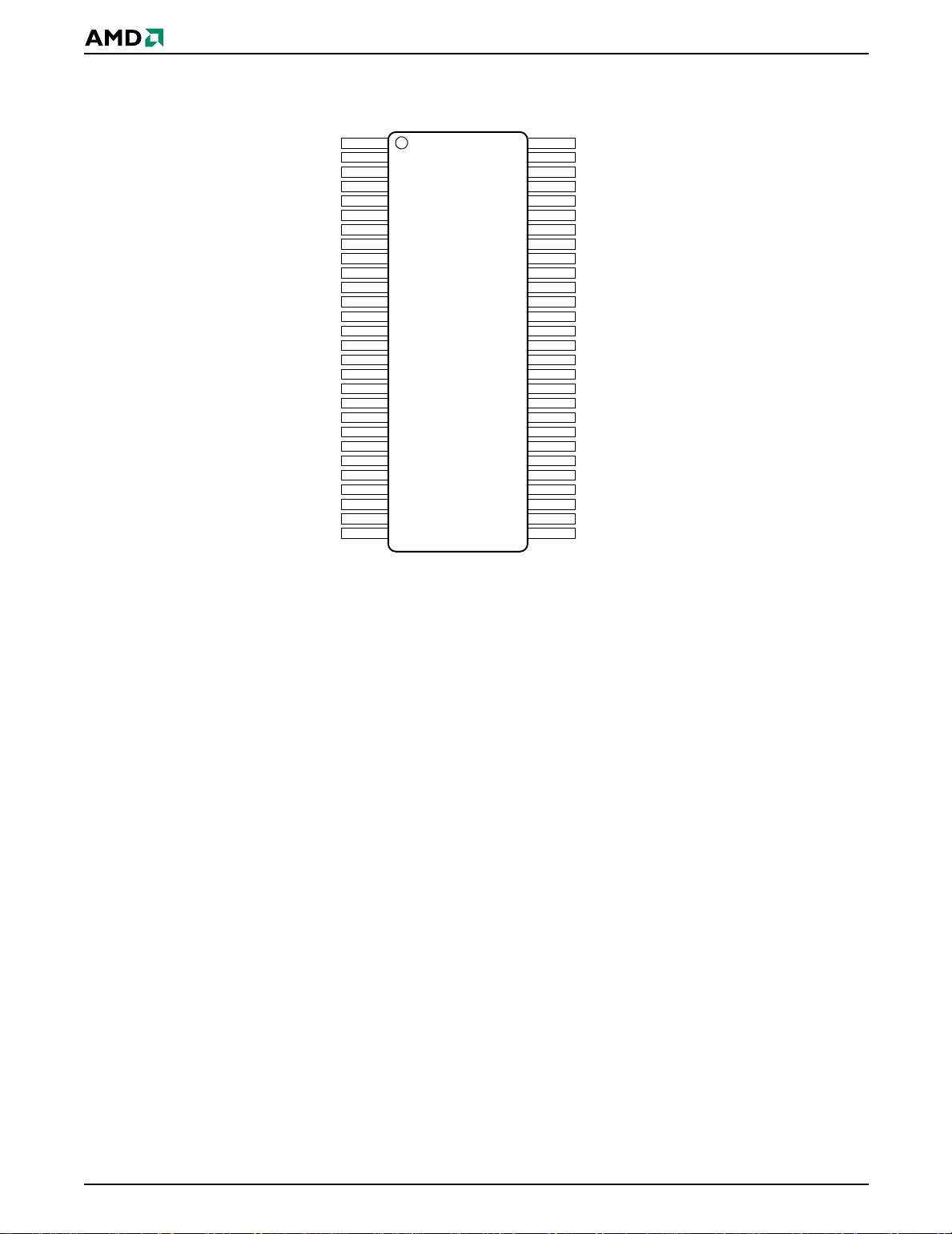
CONNECTION DIAGRAMS
ACC
WP#
A19
A18
A17
A7
A6
A5
A4
A3
A2
A1
NC
NC
NC
NC
A0
CE#
V
SS
OE#
DQ0
DQ8
DQ1
DQ9
DQ2
DQ10
DQ3
DQ11
10
11
12
13
14
15
16
17
18
19
20
21
22
23
24
25
26
27
28
1
2
3
4
5
6
7
8
9
56-Pin SSOP
(Am29LV640DH/DL
only)
56
55
54
53
52
51
50
49
48
47
46
45
44
43
42
41
40
39
38
37
36
35
34
33
32
31
30
29
RESET#
WE#
A20
A21
A8
A9
A10
A11
A12
A13
A14
A15
NC
NC
NC
NC
A16
V
IO
V
SS
DQ15
DQ7
DQ14
DQ6
DQ13
DQ5
DQ12
DQ4
V
CC
6 Am29LV640D/Am29LV641D September 20, 2002
Page 8
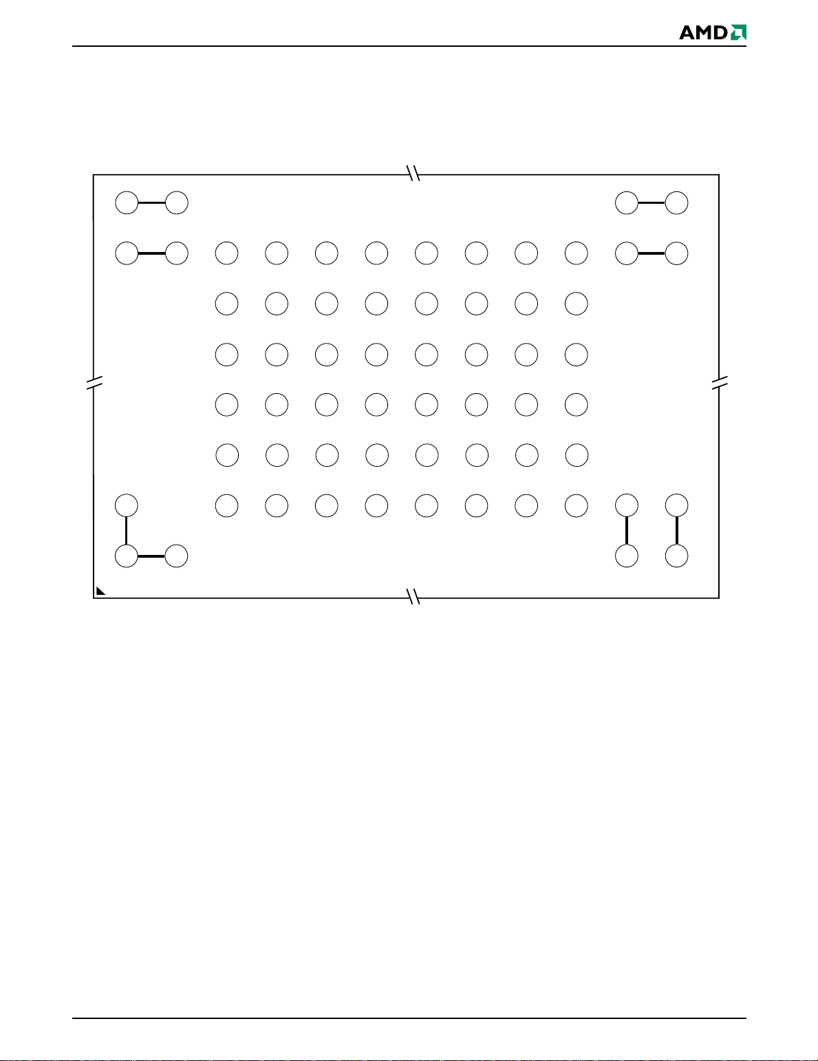
CONNECTION DIAGRAM
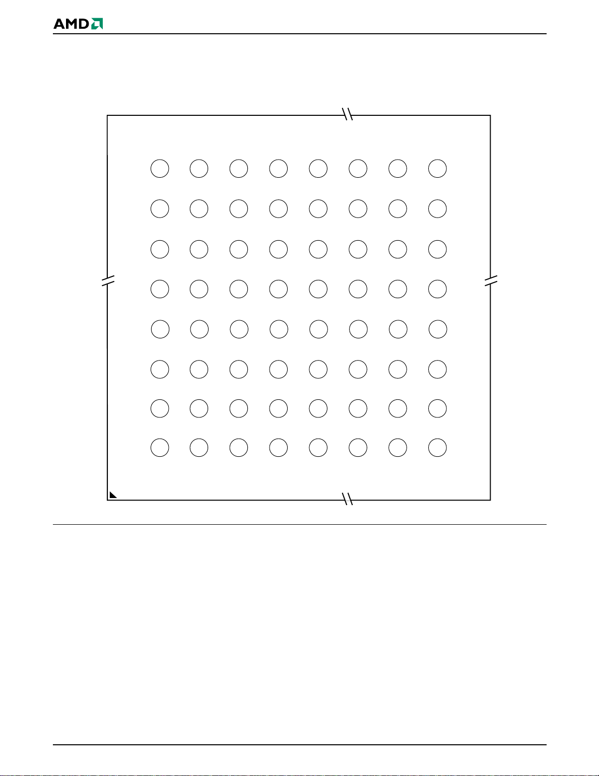
63-Ball Fine-Pitch BGA (FBGA)
Top View, Balls Facing Down
(Am29LV640DU only)
A8 B8
C7 D7A7 B7
NC NC
C6 D6 E6 F6 G6 H6 J6 K6
C5 D5 E5 F5 G5 H5 J5 K5
C4 D4 E4 F4 G4 H4 J4 K4
C3 D3 E3 F3 G3 H3 J3 K3
A2
A1 B1
NC* NC* NC* NC*
C2 D2 E2 F2 G2 H2 J2 K2
* Balls are shorted together via the substrate but not connected to the die.
E7 F7 G7 H7 J7 K7 L7
A16A15A14A12A13
DQ15
IO
DQ13 DQ6DQ14DQ7A11A10A8A9
V
CC DQ4DQ12DQ5A19A21RESET#WE#
DQ11 DQ3DQ10DQ2A20A18ACCRY/BY#
DQ9 DQ1DQ8DQ0A5A6A17A7
OE#
V
SSV
V
SSCE#A0A1A2A4A3
L8
NC* NC*NC NC
NC* NC*
L2
NC* NC*NC*
L1
M8
M7
M2
M1
September 20, 2002 Am29LV640D/Am29LV641D 7
Page 9
CONNECTION DIAGRAMS
64-Ball Fortified BGA (FBGA)
Top View , Balls Facing Down
(Am29LV640DU only)
A8
RFU
A7
A13
A6
A9
A5
WE#
A4
RY/BY#
A3
A7
A2
A3
A1
RFU
B8 C8 D8 E8 F8 G8 H8
RFURFU
B7 C7 D7 E7 F7 G7 H7
B6 C6 D6 E6 F6 G6 H6
B5 C5 D5 E5 F5 G5 H5
B4 C4 D4 E4 F4 G4 H4
B3 C3 D3 E3 F3 G3 H3
B2 C2 D2 E2 F2 G2 H2
B1 C1 D1 E1 F1 G1 H1
V
IO
SS
DQ15NCA16A15A14A12
DQ13DQ14DQ7A11A10A8
DQ12DQ5A19A21RESET#
RFURFURFURFU
IO
CC
OE#CE#A0A1A2A4
RFURFURFUV
V
SS
DQ6
DQ4V
DQ3DQ11DQ10DQ2A20A18ACC
DQ1DQ9DQ8DQ0A5A6A17
V
SS
RFURFUV
Special Handling Instructions for FBGA/fBGA Packages
Special handling is required for Flash Memory products
in BGA packages.
Flash memory devices in BGA packages may be
damaged if exposed to ultrasonic cleaning methods.
The package and/or data integrity may be compromised
if the package body is exposed to temperatures above
150°C for prolonged periods of time.
8 Am29LV640D/Am29LV641D September 20, 2002
Page 10
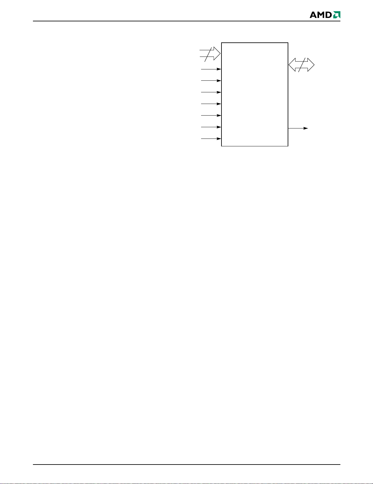
PIN DESCRIPTION
A0–A21 = 22 Addresses inputs
DQ0–DQ15 = 16 Data inputs/outputs
CE# = Chip Enable input
OE# = Output Enable input
WE# = Write Enable input
WP# = Hardware Write Protect input (N/A on
FBGA)
ACC = Acceleration Input
RESET# = H ardware Reset Pin input
RY/BY# = Ready/Busy output (FBGA only)
= 3.0 volt-only single power supply
V
CC
= Output Buffer power
V
IO
V
SS
NC = Pin Not Connected Internally
(see Product Selector Guide for
speed options and voltage
supply tolerances)
= Device Ground
LOGIC SYMBOL
22
A0–A21
CE#
OE#
WE#
WP#
ACC
RESET#
V
IO
Note: WP# is not available on the FBGA package. RY/BY#
is not available on the TSOP and SSOP packages.
DQ0–DQ15
RY/BY#
16
September 20, 2002 Am29LV640D/Am29LV641D 9
Page 11
ORDERING INFORMATION
Standard Products
AMD standard products are available in several packages and operating ranges. The order number (Valid Combination) is
formed by a combination of the following:
Am29LV640D
Am29LV641D H 90R E I N
OPTIONAL PROCESSING
Blank= Standard Processing
N = 32-byte ESN devices
(Contact an AMD representative for more information)
TEMPERATURE RANGE
I = Industrial (–40
E = Extended (–55
PACKAGE TYPE
E = 48-Pin Thin Small Outline Package (TSOP) Standard Pinout (TS 048)
F = 48-Pin Thin Small Outline Package (TSOP) Reverse Pinout (TSR048)
Z = 56-Pin Shrink Sm all Outline Package (SSO056)
PC = 64-Ball Fortified Ball Grid Array (
1.0 mm pitch, 13 x 11 mm package (LAA064)
WH = 63-Ball Fine-Pitch Ball Grid Array (FBGA)
0.80 mm pitch, 11 x 12 mm package (FBE063)
°C to +85°C)
°C to +125°C)
FBGA),
SPEED OPTION
See Product Selector Guide and Valid Combinations
SECTOR ARCHITECTURE AND SECTOR WRITE PROTECTION (WP# = 0)
H = Uniform sector device, highest address sector protecte d
L = Uniform sector device, lowest address sector protected
U = Uniform sector device (WP# not available)
DEVICE NUMBER/DESCRIPTION
Am29LV640DU/DH/DL, Am29LV641DH/DL
64 Megabit (4 M x 16-Bit) CMOS Uniform Sector Flash Memory with VersatileIO Control
3.0 Volt-only Read, Program, and Erase
Valid Combinations for
TSOP and SSOP Packages Speed/VIO Range
AM29LV640DH90R,
AM29LV640DL90R
AM29LV640DH101R,
AM29LV640DL101R
AM29LV641DH90R,
AM29LV641DL90R
AM29LV641DH101R,
AM29LV641DL101R
AM29LV640DH120R,
AM29LV640DL120R
AM29LV640DH121R,
AM29LV640DL121R
AM29LV641DH120R,
AM29LV641DL120R
AM29LV641DH121R,
AM29LV641DL121R
ZI
EI, FI
ZI, ZE
EI, FI, EE, FE
90ns,
V
= 3.0 V – 5.0 V
IO
100 ns,
V
= 1.8 V – 2.9 V
IO
90 ns
V
= 3.0 V – 5.0 V
IO
100 ns
V
= 1.8 V – 2.9 V
IO
120 ns,
V
= 3.0 V – 5.0 V
IO
120 ns,
V
= 1.8 V – 2.9 V
IO
120 ns,
V
= 3.0 V – 5.0 V
IO
120 ns
V
= 1.8 V – 2.9 V
IO
Note: LV640/641DH & DL have WP#, but no RY/BY#. U
designator in base part number replac ed by H or L.
Valid Combinations for BGA Packages
Package
Order Number
AM29LV640DU90R
AM29LV640DU101R
AM29LV640DU120R
AM29LV640DU121R
PCI L640DU90N
WHI L640DU90R
PCI L640DU01N
WHI
PCI,
PCE
WHI,
WHE
PCI,
PCE
WHI,
WHE
Marking
L640DU01R
L640DU12N
L640DU12R
L640DU21N
L640DU21R
Speed/
V
IO
90 ns, V
3.0 V – 5.0 V
I
100 ns, V
1.8 V – 2.9 V
120 ns, V
3.0 V – 5.0 V
I,
E
120 ns, V
1.8 V – 2.9 V
Range
IO
IO
IO
IO
=
=
=
=
Note: LV640DU has RY/BY#, but no WP#.
Valid Combinations
Valid Combinati ons list configurations plann ed to be supported in volume for this device. Consult the local AMD sales office to confirm
availability of specific valid combinations and to check on newly released combinations.
10 Am29LV640D/Am29LV641D September 20, 2002
Page 12
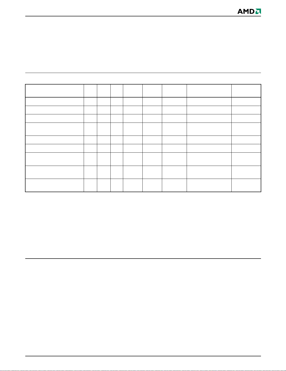
DEVICE BUS OPERATIONS
This section describes the requirements and use of
the device bus operations, which are in itiated through
the internal command register. The command register
itself does not occupy any addressabl e memory l ocation. The register is a latch used to store the commands, along with the ad dress and da ta information
needed to execute the command. The contents of the
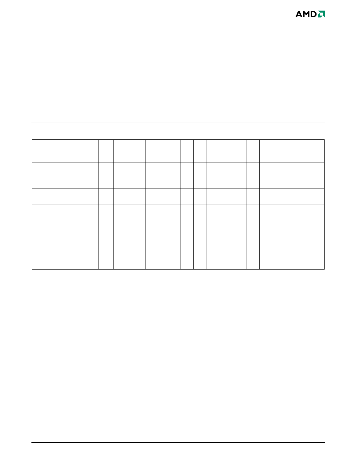
Table 1. Device Bus Operations
register serve as inputs to the intern al state machine.
The state machine outputs dictate the function of the
device. Table 1 lists the device bus operations, the inputs and control l evels they requir e, and the resultin g
output. The following subsections de scribe each of
these operations in further detail.
Operation CE# OE# WE# RESET# WP# ACC
Read L L H H
Write (Program/Erase) L H L H
Accelerated Program L H L H
±
V
Standby
Output Disable L H H H
Reset X X X L
Sector Group Protect (Note 2) L H L V
Sector Group Unprotect
(Note 2)
Temporary Sector Group
Unprotect
CC
0.3 V
XX
LHL V
XXX V
VCC ±
0.3 V
(Note 3) X
(Note 3) V
ID
ID
ID
XX
HH
XH
XX
XX
HX
HX
HX
Addresses
(Note 2)
A
IN
A
IN
A
IN
X High-Z
X High-Z
X High-Z
SA, A6 = L,
A1 = H, A0 = L
SA, A6 = H,
A1 = H, A0 = L
A
IN
DQ0–
DQ15
D
OUT
(Note 4)
(Note 4)
(Note 4)
(Note 4)
(Note 4)
Legend: L = Logic Low = VIL, H = Logic Hig h = VIH, VID = 8.5–12.5 V, VHH = 1 1. 5–12.5 V, X = Don’t Care, SA = Sector Address,
= Address In, DIN = Data In, D
A
IN
= Data Out
OUT
Notes:
1. Addresses are A21:A0. Sector addresses are A21:A15.
2. The sector protect and sector unprotect functions may al so be i mplemente d via programmi ng equipmen t. See the “Sector Group
Protection and Unprotection” sectio n.
3. If WP# = V
, the first or last sector remains protect ed. I f WP# = VIH, the first or last sector wi ll be protec ted or unprot ected as
IL
determined by the method described in “Sector Group Protection and Unprotection ”. All sectors are unprotected when shipped
from the factory (The SecSi Sector may be f actory protec ted depend ing on versi on order ed.)
4. D
IN
or D
as required by command sequence, data polling, or sector protect algorithm (see Figure 2).
OUT
VersatileIO (VIO) Control
The VersatileIO™ (VIO) control allows the host system
to set the voltage levels that the device generates and
tolerates on CE# and DQ I/O s to the same voltag e
level that is asserted on V
configurations (1.8–2.9 V and 3.0–5.0 V) for operation
in various system environments.
For example, a V
of 4.5–5.0 volts allows for I/O at
I/O
the 5 volt level, driving and receiving signals to and
from other 5 V devices on the same data bus.
. VIO is available in two
IO
Requirements for Reading Array Data
To read array data from the outputs, the system must
drive the CE# and OE# pins to V
control and selects the device. OE# is the output control and gates array data to the output pins. WE#
should remain at V
.
IH
The internal state machine is set for reading array data
upon device power-up, or after a hardware reset. This
ensures that no spurious alteration of the memory
content occurs durin g the power transition. No com-
. CE# is the power
IL
mand is necessary in this mode to obtain array data.
Standard microprocessor read cycles that assert valid
addresses on the device address inputs produce valid
September 20, 2002 Am29LV640D/Am29LV641D 11
Page 13

data on the device data outputs. The device remains
enabled for read access until the command register
contents are altered.
See “Requirements for Reading Array Data” for more
information. Refer to the AC Read-Only Operations
table for timing specifications and to F igure 13 for the
timing diagram. I
in the DC Characteristics table
CC1
represents the activ e current specific ation for r eading
array data.
Writing Commands/Command Sequences
To write a command or command sequence (which includes programming data to the device and erasing
sectors of memory), the system must drive WE# and
CE# to V
The device features an Unlock Bypass mode to facilitate faster programming. Once the device enters the
Unlock Bypass mo de, only two write cycles are required to program a word or byte, instead of four. The
“Word Program Command Sequence” section has details on programming data to the device using both
standard and Unlock Bypass command sequences.
An erase operation can erase one sector, multiple sectors, or the entire device. Table 2 indicates the address
space that each sector occupies.
I
CC2
tive current specification for the write mode. The AC
Characteristics section contains timing specification
tables and timing diagrams for write operations.
Accelerated Program Operation
The device offers accelerated program operations
through the ACC function. This function is primarily intended to allow faster manufacturing throughput during system production.
, and OE# to VIH.
IL
in the DC Characteristics table represents the ac-
lect Command Sequence sections for more inform ation.
Standby Mode
When the system is n ot reading or wri ting to the device, it can place the device in the standby mode. In
this mode, current consum ption is greatly reduc ed,
and the outputs are placed in the high impedance
state, independent of the OE# input.
The device enters the CMOS standby mode when the
CE# and RESET# pins are both held at V
± 0.3 V.
CC
(Note that this is a more restricted voltage range tha n
.) If CE# and RESET# are held at VIH, but not within
V
IH
± 0.3 V, the device will be in the s tandby mode,
V
CC
but the standby current will be greater. The device requires standard ac cess time (t
) for read access
CE
when the device is in either of these standby modes,
before it is ready to read data.
If the device is deselected during erasure or programming, the device draws active current until the
operation is completed.
in the DC Characteristics table represents the
I
CC3
standby current specification.
Automatic Sleep Mode
The automatic sleep mode minimizes Flash device energy consumption. The device automatically enables
this mode when addresses remain stable for t
30 ns. The automatic sleep mode is independent of
the CE#, WE#, and OE# control signals. Standard address access timings provide new data when addresses are changed. While in sleep mode, output
data is latched and always available to the system.
in the DC Characteristics table represents the
I
CC4
automatic sleep mode current specification.
ACC
+
If the system as serts V
matically enters the aforementioned Unlock Bypass
mode, temporarily unprotects any protected se ctors,
and uses the higher voltage on the pin to reduce the
time required for program operations. The system
would use a two-cycle pro gram comm and sequence
as required by the Unlock Bypass mode. Removing
from the ACC pin returns the device to normal op-
V
HH
eration. Note that the ACC pin must not be at V
operations other than accelerated program ming, or
device damage may result.
Autoselect Functions
If the system writes the autoselect comman d sequence, the device enters the autoselect mo de. The
system can then read autoselect codes from the internal register (which is separate from the memory array)
on DQ7–DQ0. Standard read cycle timings apply in
on this pin, the device auto-
HH
HH
for
RESET#: Hardware Reset Pin
The RESET# pin provides a hardware meth od of resetting the device to reading array data. When the RESET# pin is dri ven low for at least a perio d of t
device immediately term inates any operation in
progress, tristates all output pins, and ignores all
read/write command s for the dur ation of the RESET#
pulse. The device also resets the internal state machine to reading array data. The operation that was interrupted should be reinitiated once the device is
ready to accept another command sequence, to ensure data integrity.
Current is reduced for the duration of the RESET#
pulse. When RESET# is held at V
draws CMOS standby current (I
but not within VSS±0.3 V, the standby current will
at V
IL
±0.3 V, the device
SS
). If RESET# is held
CC4
be greater.
RP
, the
this mode. Refer to the Autoselect M ode and Auto se-
12 Am29LV640D/Am29LV641D September 20, 2002
Page 14
The RESET# pin may be tied to the system reset circuitry. A system reset would thus also reset the Flash
memory, enabling the system to read the boot-up firmware from the Flash memory.
If RESET# is a sser ted duri ng a pr ogram or eras e op-
pleted within a time of t
Algorithms). The system can read data t
RESET# pin returns to V
Refer to the AC Characteristics tables for RESET# pa-
rameters and to Figure 14 for the timing diagram.
eration, the RY/BY# pin remains a “0” (busy) until the
internal reset operation is complete, which requires a
time of t
(during Embedded Algorithms). The
READY
system can thus monitor RY/BY# to determine
whether the reset operation is complete. If RESET# is
asserted when a program or erase operation is not ex-
Output Disable Mode
When the OE# input is at VIH, output from the device is
disabled. The output pins are placed in the high
impedance state.
ecuting (RY/BY# pin is “1”), the reset operation is com-
Table 2. Sector Address Table
Sector A21 A20 A19 A18 A17 A16 A15
SA0 0000000 000000–007FFF
SA1 0000001 008000–00FFFF
SA2 0000010 010000–017FFF
SA3 0000011 018000–01FFFF
SA4 0000100 020000–027FFF
(not during Embedded
READY
.
IH
16-bit Address Range
(in hexadecimal)
after the
RH
SA5 0000101 028000–02FFFF
SA6 0000110 030000–037FFF
SA7 0000111 038000–03FFFF
SA8 0001000 040000–047FFF
SA9 0001001 048000–04FFFF
SA10 0001010 050000–057FFF
SA11 0001011 058000–05FFFF
SA12 0001100 060000–067FFF
SA13 0001101 068000–06FFFF
SA14 0001110 070000–077FFF
SA15 0001111 078000–07FFFF
SA16 0010000 080000–087FFF
SA17 0010001 088000–08FFFF
SA18 0010010 090000–097FFF
SA19 0010011 098000–09FFFF
SA20 0010100 0A0000–0A7FFF
SA21 0010101 0A8000–0AFFFF
SA22 0010110 0B0000–0B7FFF
SA23 0010111 0B8000–0BFFFF
SA24 0011000 0C0000–0C7FFF
SA25 0011001 0C8000–0CFFFF
September 20, 2002 Am29LV640D/Am29LV641D 13
Page 15
Table 2. Sector Address Table (Continued)
16-bit Address Range
Sector A21 A20 A19 A18 A17 A16 A15
SA26 0011010 0D0000–0D7FFF
SA27 0011011 0D8000–0DFFFF
SA28 0011100 0E0000–0E7FFF
SA29 0011101 0E8000–0EFFFF
SA30 0011110 0F0000–0F7FFF
SA31 0011111 0F8000–0FFFFF
SA32 0100000 100000–107FFF
SA33 0100001 108000–10FFFF
SA34 0100010 110000–117FFF
SA35 0100011 118000–11FFFF
SA36 0100100 120000–127FFF
SA37 0100101 128000–12FFFF
SA38 0100110 130000–137FFF
(in hexadecimal)
SA39 0100111 138000–13FFFF
SA40 0101000 140000–147FFF
SA41 0101001 148000–14FFFF
SA42 0101010 150000–157FFF
SA43 0101011 158000–15FFFF
SA44 0101100 160000–167FFF
SA45 0101101 168000–16FFFF
SA46 0101110 170000–177FFF
SA47 0101111 178000–17FFFF
SA48 0110000 180000–187FFF
SA49 0110001 188000–18FFFF
SA50 0110010 190000–197FFF
SA51 0110011 198000–19FFFF
SA52 0110100 1A0000–1A7FFF
SA53 0110101 1A8000–1AFFFF
SA54 0110110 1B0000–1B7FFF
SA55 0110111 1B8000–1BFFFF
SA56 0111000 1C0000–1C7FFF
SA57 0111001 1C8000–1CFFFF
SA58 0111010 1D0000–1D7FFF
SA59 0111011 1D8000–1DFFFF
SA60 0111100 1E0000–1E7FFF
14 Am29LV640D/Am29LV641D September 20, 2002
Page 16
Table 2. Sector Address Table (Continued)
16-bit Address Range
Sector A21 A20 A19 A18 A17 A16 A15
SA61 0111101 1E8000–1EFFFF
SA62 0111110 1F0000–1F7FFF
SA63 0111111 1F8000–1FFFFF
SA64 1000000 200000–207FFF
SA65 1000001 208000–20FFFF
SA66 1000010 210000–217FFF
SA67 1000011 218000–21FFFF
SA68 1000100 220000–227FFF
SA69 1000101 228000–22FFFF
SA70 1000110 230000–237FFF
SA71 1000111 238000–23FFFF
SA72 1001000 240000–247FFF
SA73 1001001 248000–24FFFF
(in hexadecimal)
SA74 1001010 250000–257FFF
SA75 1001011 258000–25FFFF
SA76 1001100 260000–267FFF
SA77 1001101 268000–26FFFF
SA78 1001110 270000–277FFF
SA79 1001111 278000–27FFFF
SA80 1010000 280000–287FFF
SA81 1010001 288000–28FFFF
SA82 1010010 290000–297FFF
SA83 1010011 298000–29FFFF
SA84 1010100 2A0000–2A7FFF
SA85 1010101 2A8000–2AFFFF
SA86 1010110 2B0000–2B7FFF
SA87 1010111 2B8000–2BFFFF
SA88 1011000 2C0000–2C7FFF
SA89 1011001 2C8000–2CFFFF
SA90 1011010 2D0000–2D7FFF
SA91 1011011 2D8000–2DFFFF
SA92 1011100 2E0000–2E7FFF
SA93 1011101 2E8000–2EFFFF
SA94 1011110 2F0000–2F7FFF
SA95 1011111 2F8000–2FFFFF
September 20, 2002 Am29LV640D/Am29LV641D 15
Page 17
Table 2. Sector Address Table (Continued)
16-bit Address Range
Sector A21 A20 A19 A18 A17 A16 A15
SA96 1100000 300000–307FFF
SA97 1100001 308000–30FFFF
SA98 1100010 310000–317FFF
SA99 1100011 318000–31FFFF
SA100 1100100 320000–327FFF
SA101 1100101 328000–32FFFF
SA102 1100110 330000–337FFF
SA103 1100111 338000–33FFFF
SA104 1101000 340000–347FFF
SA105 1101001 348000–34FFFF
SA106 1101010 350000–357FFF
SA107 1101011 358000–35FFFF
SA108 1101100 360000–367FFF
(in hexadecimal)
SA109 1101101 368000–36FFFF
SA110 1101110 370000–377FFF
SA111 1101111 378000–37FFFF
SA112 1110000 380000–387FFF
SA113 1110001 388000–38FFFF
SA114 1110010 390000–397FFF
SA115 1110011 398000–39FFFF
SA116 1110100 3A0000–3A7FFF
SA117 1110101 3A8000–3AFFFF
SA118 1110110 3B0000–3B7FFF
SA119 1110111 3B8000–3BFFFF
SA120 1111000 3C0000–3C7FFF
SA121 1111001 3C8000–3CFFFF
SA122 1111010 3D0000–3D7FFF
SA123 1111011 3D8000–3DFFFF
SA124 1111100 3E0000–3E7FFF
SA125 1111101 3E8000–3EFFFF
SA126 1111110 3F0000–3F7FFF
SA127 1111111 3F8000–3FFFFF
Note: All sectors are 32 Kwords in size.
16 Am29LV640D/Am29LV641D September 20, 2002
Page 18
Autoselect Mode
The autoselect mode provides manufacturer and device identification, and sector protection verification,
through identifier codes output on DQ7–DQ0. This
mode is prim arily intend ed for progr amming equi pment to automatically match a device to be programmed with its corresponding programming
algorithm. However, the autoselect codes can also be
accessed in-system through the command register .
When using programming equipment, the autoselect
mode requires V
Address pins A6, A1, and A0 must be as shown in
Description CE# OE# WE#
Manufacturer ID: AMD L L H X X V
Device ID: LV640DU/H/L,
LV641DH/L
Sector Protection
Verification
SecSi Sector Indicator Bit
(DQ7), WP# protects
highest address sector
(LV640DH/641DH), or
no WP# (LV640DU)
SecSi Sector Indicator Bit
(DQ7), WP# protects
lowest address sector
(LV640DL/641DL)
(8.5 V to 12.5 V) on address pin A9.
ID
Tabl e 3. Autoselect Codes, (High Voltage Method)
A21
to
A15
LLH X XV
LLHSAXV
LLH X XV
LLH X XV
A14
to
A10 A9
Table 3. In addition, when verifying sector protection,
the sector address must appear on the appropriate
highest order address bits (see Table 2). Table 3
shows the rema ining a ddress b its that ar e don’t care.
When all necessary bits have been set as required,
the programming equipment may then read the corresponding identifier code on DQ7–DQ0.
To access the autoselect codes in-system, the host
system can issue the autoselect command via the
command register, as shown in Table 10. This method
does not require V
. Refer to the Autoselect Com-
ID
mand Sequence section for more information.
A8
to
A7 A6
XLXLL 0001h
ID
XLXLH 22D7h
ID
XLXHL
ID
XLXHH
ID
XLXHH
ID
A5
to
A2 A1 A0 DQ15 to DQ0
XX01h (protected),
XX00h (unprotected)
XX98h (factory locked),
XX18h (not factory locked)
XX88h (factory locked),
XX08h (not factory locked)
Legend: L = Logic Low = VIL, H = Logic High = VIH, SA = Sector Address, X = Don’t care.
September 20, 2002 Am29LV640D/Am29LV641D 17
Page 19

Sector Group Protection and Unprotection
The hardware sector group protection feature disables
both program and erase operations in any sector
group. In this device, a sector group consists of fou r
adjacent sectors that are protected or unprotected at
the same time (see Table 4). The hardware sector
group unprotection feature re -enables both program
and erase operations in previously protected sector
groups. Sector group protection/unprotection can be
implemented via two methods.
Sector protection/unprotection requires V
SET# pin only, and can be implemented either in-system or via progr amming eq uipment. Figure 2 sh ows
the algorithms and Figure 22 shows the timing diagram. This method uses standard microprocessor bus
cycle timing. For sector group unprotect, all unprotected sector groups must first be protected prior to
the first sector group unprotect write cycle.
The device is shipped with all se ctor groups unprotected. AMD offers the option of programming and
protecting sector groups at its factory prior to shipping
the device through AMD’s ExpressFlash™ Service.
Contact an AMD representative for details.
It is possible to determin e whether a se ctor group is
protected or unprotected. See the Autoselect Mode
section for details.
on the RE-
ID
Table 4. Sector Group Protection/Unprotection
Address Table
Sector Group A21–A17
SA0–SA3 00000
SA4–SA7 00001
SA8–SA11 00010
SA12–SA15 00011
SA16–SA19 00100
SA20–SA23 00101
SA24–SA27 00110
SA28–SA31 00111
SA32–SA35 01000
SA36–SA39 01001
SA40–SA43 01010
SA44–SA47 01011
SA48–SA51 01100
SA52–SA55 01101
SA56–SA59 01110
SA60–SA63 01111
SA64–SA67 10000
SA68–SA71 10001
SA72–SA75 10010
SA76–SA79 10011
SA80–SA83 10100
SA84–SA87 10101
SA88–SA91 10110
SA92–SA95 10111
SA96–SA99 11000
SA100–SA103 11001
SA104–SA107 11010
SA108–SA111 11011
SA112–SA115 11100
SA116–SA119 11101
SA120–SA123 11110
SA124–SA127 11111
Note: All sector groups are 128 Kwords in size.
18 Am29LV640D/Am29LV641D September 20, 2002
Page 20

Write Protect (WP#)
The Write Protect function provides a hardware
method of protecting the first or last sector without
using V
If the system asserts V
.
ID
on the WP# pin, the device
IL
disables program and erase functions in the first or
last sector independently of whether those sectors
were protected or unprotected using the method described in “Sector Group Protection and Unprotecti on”.
Note that if WP# is at V
when the device is in th e
IL
standby mode, the maximum input load current is increased. See the table in “DC Characteristics”.
If the system asserts V
on the WP# pin, the device
IH
reverts to whether the first or last sector was previously set to be protected or unprotected using the
method described in “Sector Group Protection and Unprotection”.
Temporary Sector Group Unprotect
(Note: In this device, a sector group consists of four adjacent
sectors that are prote cted or unprotected at the same ti me
(see Table 4)).
This feature allo ws tempora ry unprotecti on of previously protected sector groups to change data in-system. The Sector Group Unprotect mode is act ivated by
setting the RESET# pin to V
this mode, formerly protected sector groups can be
programmed or erased by selecting the sector group
addresses. Once V
is removed from the RES ET#
ID
pin, all the previously protected sector groups are
protected again. Figure 1 shows the algorithm, and
Figure 21 shows the timing diagrams, for this feature.
(8.5 V – 12.5 V). During
ID
START
RESET# = V
(Note 1)
Perform Erase or
Program Operations
RESET# = V
Temporary Sector
Group Unprotect
Completed (Note 2)
Notes:
1. All protected sector groups unprotected (If WP# = V
the first or last sector will remain protected).
2. All previously protect ed sec tor gro ups are prote cte d
once again.
ID
IH
Figure 1. Temporary Sector Group
Unprotect Operation
,
IL
September 20, 2002 Am29LV640D/Am29LV641D 19
Page 21

Temporary Sector
Group Unprotect
Mode
Increment
PLSCNT
START
PLSCNT = 1
RESET# = V
Wait 1 µs
No
First Write
Cycle = 60h?
Set up sector
group address
Sector Group Protect:
Write 60h to sector
group address with
A6 = 0, A1 = 1,
A0 = 0
Wait 150 µs
Verify Sector Group
Protect: Write 40h
to sector group
address twith A6 = 0,
A1 = 1, A0 = 0
Yes
START
Protect all sector
groups: The indicated
ID
Reset
PLSCNT = 1
portion of the sector
group protect algorithm
must be performed for all
unprotected sector
groups prior to issuing
the first sector group
unprotect address
PLSCNT = 1
RESET# = V
Wait 1 µs
First Write
Cycle = 60h?
All sector
No
protected?
Set up first sector
group address
Sector Group
Unprotect:
Write 60h to sector
group address with
A6 = 1, A1 = 1,
Wait 15 ms
groups
A0 = 0
Yes
Yes
ID
Temporary Sector
No
Group Unprotect
Mode
No
PLSCNT
= 25?
Yes
Device failed
Sector Group
Protect
Algorithm
Read from
sector group address
with A6 = 0,
A1 = 1, A0 = 0
No
Data = 01h?
Protect
another
sector group?
Remove V
from RESET#
Write reset
command
Sector Group
Protect complete
Yes
No
Verify Sector Group
Unprotect: Write
40h to sector group
Increment
PLSCNT
No
Yes
ID
PLSCNT
= 1000?
Yes
Device failed
Sector Group
address with
A6 = 1, A1 = 1,
A0 = 0
Read from
sector group
address with A6 = 1,
A1 = 1, A0 = 0
No
Data = 00h?
Last sector
group
verified?
Remove V
from RESET#
Yes
Yes
Set up
next sector group
address
No
ID
Unprotect
Algorithm
Write reset
command
Sector Group
Unprotect complete
Figure 2. In-System Sector Group Protect/Unprotect Algorithms
20 Am29LV640D/Am29LV641D September 20, 2002
Page 22

SecSi (Secured Silicon) Sector Flash
Memory Region
The SecSi (Secured Silicon) Sector feature provides a
Flash memory region that enables permanent part
identification through an Electronic Serial Number
(ESN). The SecSi Sector is 128 words in length, and
uses a SecSi Sector Indicator Bit (DQ7) to indicate
whether or not the SecSi Sector is locked when
shipped from the factory. This bit is permanently set at
the factory and cannot be changed, which prevents
cloning of a factory locked part. This ensures the security of the ESN once the product is shipped to the fie ld.
AMD offers the device with the SecSi Sector either
factory locked or customer lockable. The factory-locked version is alw ays protected when shipped
from the factory, and has the SecSi (S ecured Silicon )
Sector Indicator Bit permanently set to a “1.” The customer-lockable version is shipped with the SecSi Sector unprotected, allo wing customers to u tilize that
sector in any manner they choose. The customer-lockable version also has the SecSi Sector Indicator Bit
permanently set to a “0.” Thu s, the SecSi Sector Indicator Bit prevents customer-lockable devices from
being used to replace devices that are factory locked.
The SecSi sector address space in this device is allocated as follows:
Table 5. SecSi Sector Contents
SecSi Sector
Address Range
000000h–000007h ESN
000008h–00007Fh Unavailable
Standard
Factory Locked
ExpressFlash
Factory Locked
ESN or
determined by
customer
Determine d by
customer
Customer
Lockable
Determined by
customer
vices are then shipped from AMD’s factory with the
SecSi Sector permanently locked. Contact an AMD
representative for details on using AMD’s ExpressFlash service.
Customer Lockable: SecSi Sector NOT
Programmed or Protected At the Factory
As an alternative to the factory-locked version, the device may be ordered such that the customer may program and protect the 128-word SecSi sector.
Programming and protecting the SecSi S ector must be
used with caution since, once protected, there is no
procedure available for unprotecting the SecSi Sector
area and none of the bits in the SecSi Sector memory
space can be modified in any way.
The SecSi Sector area can be prote cted using one of
the following procedures:
■ Write the three-cycle Enter SecSi Sector Region
command sequence, and then follow the in-system
sector protect algorithm as shown in Figure 2, except that RESET# may be at either V
or VID. This
IH
allows in-system protection of the SecSi Sector
without raising any device pin to a high voltage.
Note that this method is only applicabl e to the SecSi
Sector.
■ Write the three-cycle Enter SecSi Sector Region
command sequence, and then use the alternate
method of sector protection described in the “Sector
Group Protection and Unprotection” section.
Once the SecSi Secto r is programmed, loc ked and
verified, the system must write the Exit SecSi Sector
Region command sequence to return to reading and
writing within the remainder of the array.
The system accesses the SecSi Sector through a
command sequence (see “Enter SecSi Sector/Exit
SecSi Sector Command Sequence”). After the system
has written the Enter SecSi Sector command sequence, it may read the SecSi Sector by using the addresses normally occupied by the first sector (SA0).
This mode of operation continues until the system issues the Exit SecSi Sector command sequ ence, or
until power is removed from the device. On power-up,
or following a hardware reset, the device reverts to
sending commands to sector SA0.
Factory Locked: SecSi Sector Programmed and
Protected At the Factory
In devices with an ESN, the SecSi Sector is protected
when the device is shipped from the f a ctory. The SecSi
Sector cannot be modified in any way. A factory locked
device has an 8-word random E SN at addresses
000000h–000007h.
Customers may opt to have their code programmed by
AMD through the AMD ExpressFlash service. The de-
Hardware Data Protection
The command sequence requirement of unlock cycles
for programming or erasing provides data pro tection
against inadvertent writes (refer to Table 10 for command definitions). In addition, the following hardware
data protection measures prevent accidental erasure
or programming, which might otherwise be caused by
spurious system level signals during V
and power-down transitions, or from system noise.
Low V
When V
Write Inhibit
CC
is less than V
CC
, the device does not ac-
LKO
cept any write cycles. This protects data during V
power-up and power-down. The command register
and all internal program/erase circuits are disabled,
and the device resets to the read mode. Subsequent
writes are igno red until V
is greater than V
CC
system must provide the proper signals to the control
pins to prevent unintentional writes when V
greater than V
LKO
.
power-up
CC
LKO
CC
. The
is
CC
September 20, 2002 Am29LV640D/Am29LV641D 21
Page 23

Write Pulse “Glitch” Protection
Noise pulses of less than 5 ns (typical) on OE#, CE#
or WE# do not initiate a write cycle.
Logical Inhibit
Write cycles are inhibited by holding any one of OE# =
, CE# = VIH or WE# = VIH. To initiate a write cycle,
V
IL
COMMON FLASH MEMORY INTERFACE (CFI)
The Common Flash Interface (CFI) specification outlines device and host system software interrogation
handshake, which allows specific vendor-specified
software algorithms to be used for entire families of
devices. Software support can then be device-independent, JEDEC ID-independent, and forward- and
backward-comp atible for the spe cified flash dev ice
families. Flash vendors can sta ndardiz e their existing
interfaces for long-term compatibility.
This device enters the CFI Query mode when the system writes the CFI Query command, 98h, to address
55h, any time the device is ready to read array data.
The system can read CFI information at the addresses
CE# and WE# must be a logical zero while OE# is a
logical one.
Power-Up Wri t e Inhibit
If WE# = CE# = V
and OE# = VIH during power up,
IL
the device does not accept commands on the rising
edge of WE#. The internal s tate machine is automatically reset to the read mode on power-up.
given in Tables 6–9. To terminate readi ng CFI d ata,
the system must write the reset command.
The system can also write the CFI query command
when the device is in the autoselect mode. The device
enters the CFI qu ery mod e, and th e syste m can r ead
CFI data at the addresses given in Tables 6–9. The
system must write the reset command to return the device to the autoselect mode.
For further information, please refer to the CFI Specification and CFI Publication 100, available via the
World Wide Web at http://www.amd.com/products/nvd/overview/cfi.html. Alternatively, contact an
AMD representative for copies of these documents.
Table 6. CFI Query Identification String
Addresses (x16) Data Description
10h
11h
12h
13h
14h
15h
16h
17h
18h
19h
1Ah
0051h
0052h
0059h
0002h
0000h
0040h
0000h
0000h
0000h
0000h
0000h
Query Unique ASCII string “QRY”
Primary OEM Command Set
Address for Primary Extende d Table
Alternate OEM Command Set (00h = none exists)
Address for Alternate OEM Extended Table (00h = none exists)
22 Am29LV640D/Am29LV641D September 20, 2002
Page 24

Table 7. System Interface String
Addresses (x16) Data Description
V
Min. (write/erase)
1Bh 0027h
1Ch 0036h
CC
D7–D4: volt, D3–D0: 100 millivolt
Max. (write/erase)
V
CC
D7–D4: volt, D3–D0: 100 millivolt
1Dh 0000h V
1Eh 0000h V
1Fh 0004h Typical timeout per single byte/word write 2
20h 0000h Typical timeout for Min. size buffer write 2
21h 000Ah Typical timeout per individual block erase 2
22h 0000h Typical timeout for full chip erase 2
23h 0005h Max. timeout for byte/word write 2
24h 0000h Max. timeout for buffer write 2
25h 0004h Max. timeout per individual block erase 2
26h 0000h Max. timeout for full chip erase 2
Min. voltage (00h = no VPP pin present)
PP
Max. voltage (00h = no VPP pin present)
PP
N
ms (00h = not supported)
N
times typical
N
times typical
N
times typical (00h = not supported)
N
µs
N
µs (00h = not supported)
N
ms
N
times typical
Table 8. Device Geometry Definition
Addresses (x16) Data Description
27h 0017h Device Size = 2
28h
29h
2Ah
2Bh
0001h
0000h
0000h
0000h
Flash Device Interface description (refer to CFI publication 100)
Max. number of byte in multi-byte write = 2
(00h = not supported)
N
byte
N
2Ch 0001h Number of Erase Block Regions within device
2Dh
2Eh
2Fh
30h
31h
32h
33h
34h
35h
36h
37h
38h
39h
3Ah
3Bh
3Ch
007Fh
0000h
0000h
0001h
0000h
0000h
0000h
0000h
0000h
0000h
0000h
0000h
0000h
0000h
0000h
0000h
Erase Block Region 1 Information
(refer to the CFI specification or CFI publication 100)
Erase Block Region 2 Information (refer to CFI publication 100)
Erase Block Region 3 Information (refer to CFI publication 100)
Erase Block Region 4 Information (refer to CFI publication 100)
September 20, 2002 Am29LV640D/Am29LV641D 23
Page 25

Table 9. Primary Vendor-Specific Extended Query
Addresses (x16) Data Description
40h
41h
42h
43h 0031h Major version number, ASCII
44h 0033h Minor version number, ASCII
45h 0000h
46h 0002h
47h 0004h
48h 0001h
49h 0004h
4Ah 0000h
4Bh 0000h
4Ch 0000h
0050h
0052h
0049h
Query-unique ASCII string “PRI”
Address Sensitive Unlock (Bits 1-0)
00b = Required, 01b = Not Required
Silicon Revision Number (Bits 7-2) 000000b = 0.23 µm Process Technology
Erase Suspend
00 = Not Supported, 01 = To Read Only, 02 = To Read & Write
Sector Protect
00 = Not Supported, X = Number of sectors in per group
Sector Temporary Unprotect
00 = Not Supported, 01 = Supported
Sector Protect/Unprotect scheme
04 = 29LV800A mode
Simultaneous Operation
00 = Not Supported, XX = Number of Sectors in Bank
Burst Mode Type
00 = Not Supported, 01 = Supported
Page Mode Type
00 = Not Supported, 01 = 4 Word Page, 02 = 8 Word Page
4Dh 00B5h
4Eh 00C5h
4Fh 000Xh
ACC (Acceleration) Supply Minimum
Bits 7–4 = Hex Value in Volts, Bits 0–3 = BCD Value in 100 mV
ACC (Acceleration) Supply Maximum
Bits 7–4 = Hex Value in Volts, Bits 0–3 = BCD Value in 100 mV
Top/Bottom Boot Sector Flag
00h = Uniform Sector, No WP# Control
04h = Uniform Sector, WP# Protects Bottom Sector
05h = Uniform Sector, WP# Protects Top Sector
COMMAND DEFINITIONS
Writing specific address and data commands or sequences into the command register initiates device operations. Table 10 defines the valid register command
sequences. Writing incorrect address and data val-
ues or writing them in the improper sequence resets
the device to reading array data.
All addresses are latched on the falling edge of WE#
or CE#, whichever happens later. All dat a is latched on
the rising edge of WE# or CE#, whichever happens
first. Refer to the AC Characteristics section for timing
diagrams.
Reading Array Data
The device is automatically set to reading array data
after device power-up. No commands are required to
retrieve data. The device is ready to read array data
after completing an Embedded Program or Embedded
Erase algorithm.
After the device accepts an Erase Suspend command,
the device enters the erase-suspend-read mode, after
which the system can read data from any
non-erase-suspended sector. After completing a programming operation in the Erase Suspend mode, the
system may once again read array data with the same
exception. See the Erase Suspend/Erase Resume
Commands section for more information.
24 Am29LV640D/Am29LV641D September 20, 2002
Page 26

The system must issue the reset command to return
the device to the read (or erase-suspend-read) mode
if DQ5 goes high during an active program or erase
operation, or if the device i s in the autoselect mod e.
See the next section, Reset Command, for more information.
See also Requirements for Reading Array Data in the
Device Bus Operations section for more information.
The Read-Only Operations table provides the read parameters, and Figure 13 shows the timing diagram.
Reset Command
Writing the reset command resets the device to the
read or erase-sus pend-read mod e. Address bi ts are
don’t cares for this command.
The reset command may be written between the sequence cycles in an erase command sequence before
erasing begins. This resets the device to the read
mode. Once erasure begins, however, the device ignores reset commands until the operation is complete.
The reset command may be w ritten between the
sequence cycles in a program command sequence
before programming begins. This resets the devic e to
the read mode. If the pr ogram com mand sequ ence is
written while the device is in the Erase Suspend mode,
writing the reset comma nd returns the device to th e
erase-suspend-re ad mode. Once pr ogramming b egins, however, the device ignores reset commands
until the operation is complete.
The reset command may be written between the sequence cycles in an autoselect command sequence.
Once in the autoselect mode, the reset command
must be written to return to the read mode. If the device entered the autosele ct mode whi le in the Erase
Suspend mode, writing the reset command returns the
device to the erase-suspend-read mode.
If DQ5 goes high during a program or erase operation,
writing the reset comma nd returns the device to th e
read mode (or erase-suspend-read mode if the device
was in Erase Suspend).
Autoselect Command Sequence
The autoselect command sequence allows the host
system to access the manufacturer and device codes,
and determine whether or not a sector is protected.
Table 10 shows the address and data requ irements.
This method is an alternative to that shown in Table 3,
which is intended for PROM programmers and requires V
mand sequence may be written to an address that is
either in the read or eras e-suspend-rea d mode. The
autoselect command may not be wri tten while the device is actively programming or erasing.
on address pin A9. The autoselect com-
ID
The autoselect command sequence is initiated by first
writing two unlock cycles. This is followed by a third
write cycle that contains the autoselect command. The
device then enters the autoselect mode. The system
may read at any address any number of times without
initiating another autoselect command sequence:
■ A read cycle at address XX00h returns the manufacturer code.
■ A read cycle at address XX01h returns the device
code.
■ A read cycle to an address containing a sector
group address (SA), and the address 02h on A7 –A0
returns 01h if the sector group is protected, or 00h
if it is unprotected. (Refer to Table 4 for valid sector
addresses).
The system must write the reset command to return to
the read mode (or erase-suspend-read mode if the device was previously in Erase Suspend).
Enter SecSi Sector/Exit SecSi Sector
Command Sequence
The SecSi Sector region provides a secured data area
containing an 8-word random Electronic Serial Number (ESN). The system can access the SecSi Sector
region by issuing the three-cycle Enter SecSi Sector
command sequence. The device continues to access
the SecSi Sector region until the system issues the
four-cycle Exit SecSi Sector command sequence. The
Exit SecSi Sector command sequence returns the device to norm al op eratio n. Table 10 shows the address
and data requirements for both command sequences.
See also “SecSi (Secured Silicon) Sector Flash
Memory Region” for further information.
Word Program Command Sequence
Programming is a four-bus-cycle operation. The program command sequence is initiated by writing two
unlock write cycles, followed by the program set-up
command. The program addr ess and data are wr itten
next, which in turn in itiate the Em bedded Program a lgorithm. The system i s not required to provide furthe r
controls or timings. The device automatically provides
internally generated program puls es and verifies the
programmed cell margin. Table 10 shows the address
and data requirements for the byte program command
sequence.
When the Embedded Program algorithm is complete,
the device then returns to the read mode and addresses are no longer latched. The system can determine the status of the program operation by using
DQ7, DQ6, or RY/BY#. Refer to the Write Operation
Status section for information on these status bits.
Any commands w ritten to the device during the Embedded Program Algorithm are ignored. Note th at a
September 20, 2002 Am29LV640D/Am29LV641D 25
Page 27

hardware reset immediately terminates the program
operation. The program command sequence should
be reinitiated once the device has returned to the read
mode, to ensure data integrity.
Programming is allowed in any sequence and across
sector boundaries. A bit cannot be programmed
from “0” back to a “1.” Attempting to do so may
cause the device to set DQ5 = 1, or cause the DQ7
and DQ6 status bits to indicate the operation was successful. However, a succeeding read will show t hat the
data is still “0.” On ly erase ope rations can co nvert a
“0” to a “1.”
Unlock Bypass Command Sequence
The unlock bypass feature allows the system to program words to the device faster than using the standard program command s equence. The unlock
bypass command se quence is in itiated by firs t writing
two unlock cycles. This is followed by a third write
cycle containing the unlock bypass command, 20h.
The device then enters the unlock bypass mo de. A
two-cycle unlock bypass program command sequence
is all that is required to program in this mode. The first
cycle in this sequence contains the unlock bypass program command, A0h; the second cycle contains the
program address and data. Additional data is programmed in the same manner. This mode dispenses
with the initial two unlock cycles required in the standard program command sequence, resulting in faster
total programming time. Table 10 shows the requirements for the command sequence.
During the unlock bypass mode, only the Unlock Bypass Program and Unlock Bypas s Reset comma nds
are valid. To exit the unlock bypass mode, the system
must issue the two-cycle unlock bypass reset command sequence. The first cycle must contain the data
90h. The second cycle must contain the data 00h. The
device then returns to the read mode.
The device offers accelerated program operations
through the ACC pin. When the system asserts V
HH
on
the ACC pin, the device automatically enters the Unlock Bypass mode. The system may then write the
two-cycle Unlock Bypass pr ogram command sequence. The device uses the higher voltage on the
ACC pin to accelerate the operation. Note that the
ACC pin must not be at V
for operations other than
HH
accelerated programming, or device damage may result.
Figure 3 illustrates the algorithm for the program operation. Refer to the Erase and Program Operations
table in the AC Characteristics section for parameters,
and Figure 15 for timing diagrams.
START
Write Program
Command Sequence
Data Poll
Embedded
Program
algorithm
in progress
Increment Address
Note: See Table 10 for program command sequence.
No
from System
Verify Data?
Yes
Last Address?
Yes
Programming
Completed
No
Figure 3. Program Operation
Chip Erase Command Sequence
Chip erase is a six bus cycle operation. The chip erase
command sequence is initiated by writing two unlock
cycles, followed by a set-up command. Two additional
unlock write cycles are then followed by the chip erase
command, which in turn invokes the Embedded Erase
algorithm. The device does not require the system to
preprogram prior to erase. The Embedded Erase algorithm automatically preprograms and verifies the entire
memory for an all zero data pattern prior to electrical
erase. The system is not required to provide any controls or timings during these operations. Table 10
shows the address and data requirements for the chip
erase command sequence.
26 Am29LV640D/Am29LV641D September 20, 2002
Page 28

When the Embedded Erase algorithm is complete, the
device returns to the read mode and add resses are no
longer latched. The system can determine the status
of the erase operation by using DQ7, DQ6, DQ2, or
RY/BY#. Refer to the Write Operation Status section
for information on these status bits.
Any commands written during the chip erase operation
are ignored. However, note that a hardware reset im-
mediately termina tes the erase operation. If tha t occurs, the chip erase command sequence should be
reinitiated once the device has returned to reading
array data, to ensure data integrity.
Figure 4 illustrates the algorithm for the erase operation. Refer to the Erase and Program Operation s tables in the AC Characteristics sectio n for parameters,
and Figure 17 section for timing diagrams.
Sector Erase Command Sequence
Sector erase is a six bus cycle operation. The sector
erase command sequence is initiated by writing two
unlock cycles, followed by a set-up command. Two additional unlock cycles are written, and are then followed by the address of the sector to be erased, and
the sector erase command. Table 10 shows the address and data requirements for the sector erase command sequence.
The device does not require the system to preprogram
prior to erase. The Embedded Erase algorithm automatically programs and v erifies the entire m emory for
an all zero data pattern prior to electrica l erase. The
system is not required to provide any controls or timings during these operations.
After the command sequence is written, a sector erase
time-out of 50 µs occurs. During the time-out period,
additional sector addresses and sector erase com mands may be written. Loading the sector e rase buf fer
may be done in any sequence, and the number of sectors may be from one sector to all sectors. The time
between these additional cycles must be less than 50
µs, otherwise erasure may begin. Any sector erase
address and command following the exceeded
time-out may or may not be accepted. It is recommended that processor interrupts be disabled during
this time to ensure all comm ands are accepted . The
interrupts can be re-enabled after the last Sector
Erase command is written. Any command other than
Sector Erase or Erase Suspend during the
time-out period resets the device to the read
mode. The system must rewrite the command se-
quence and any additional addresses and commands.
The system can monitor DQ3 to determine if the sec-
tor erase timer has timed out (See the section on DQ3:
Sector Erase Timer.). The time-out begins from th e rising edge of the final WE# pulse in the command
sequence.
When the Embedded Erase algorithm is complete, the
device returns to reading array data and addresses
are no longer latched. The system can determine the
status of the er ase operati on by rea ding DQ7, D Q6,
DQ2, or RY/BY#. Note that while t he Embedded Er ase
operation is in progress, the system can read data
from the non-erasing sector. Refer to the Write Operation Status section for information on these status bits.
Once the sector erase operation has begun, only the
Erase Suspend command is valid. All other commands are ignored. However, note that a hardware
reset immediately terminates the erase operation. If
that occurs, the sector erase command seq uence
should be reinitiated once the device has returned to
reading array data, to ensure data integrity.
Figure 4 illustrates the algorithm for the erase operation. Refer to the Erase and Program Operatio ns tables in the AC Characteristics sectio n for parameters,
and Figure 17 section for timing diagrams.
Erase Suspend/Erase Resume Commands
The Erase Suspend command, B0h, allows the system to interrupt a sector erase operation and then read
data from, or program data to, any sector not selected
for erasure. This command is valid only during the
sector erase operation, including the 50 µs time-out
period during the sector erase command sequence.
The Erase Suspend command is ignored if written during the chip erase operation or Embedded Program
algorithm.
When the Erase Suspend command is written during
the sector erase operation, the device requires a maximum of 20 µs to suspend the erase operation. However, when the Erase Suspend command is written
during the sector erase time-out, the device immediately terminates the time-out period and suspends the
erase operation.
After the erase operation has been suspended, the
device enters the erase-suspend-read mode. The system can read data from or program data to any sector
not selected for erasure. (The device “erase suspends” all sectors selected for erasure.) Reading at
any address with in erase-suspende d sectors produces status information on DQ7–DQ0. The system
can use DQ7, or DQ6 and DQ2 together, to determine
if a sector is actively erasing or is erase-sus pended.
Refer to the Write Operation Status section for information on these status bits.
After an eras e-sus pende d prog ram o pera tion is complete, the device returns to the erase-suspend-read
mode. The system can determine the status of the
program operation using the DQ7 or DQ6 status bits,
just as in the standard word program operation.
September 20, 2002 Am29LV640D/Am29LV641D 27
Page 29

Refer to the Write Operation Status section for more
information.
In the erase-suspend-read mode, the system can also
issue the autoselect command sequence. Refer to the
Autoselect Mode and Autoselect Command Sequence
sections for details.
To resume the sector erase operation, the system
must write the Erase Resume command. The address
of the erase-suspended sector is required when writing this command. Further writes of the Resume command are ignored. Another Erase Suspend com mand
can be written after the chip has resumed erasing.
START
Write Erase
Command Sequence
(Notes 1, 2)
Data Poll to Erasing
Bank from System
No
Notes:
1. See Table 10 for erase command sequence.
2. See the section on DQ3 for information on the sector
erase timer.
Data = FFh?
Yes
Erasure Completed
Embedded
Erase
algorithm
in progress
Figure 4. Erase Operation
28 Am29LV640D/Am29LV641D September 20, 2002
Page 30

Command Definitions
Table 10. Command Definitions
Bus Cycles (Notes 1–4)
Command
Sequence
Read (Note 5) 1 RA RD
Reset (Note 6) 1 XXX F0
Manufacturer ID 4 555 AA 2AA 55 555 90 X00 0001
Device ID 4 555 AA 2AA 55 555 90 X01 22D7
SecSi Sector Factory
Protect (Note 8)
Sector Group Protect Verify
(Note 9)
Autoselect (Note 7)
Enter SecSi Sector Region 3 555 AA 2AA 55 555 88
Exit SecSi Sector Region 4 555 AA 2AA 55 555 90 XXX 00
Program 4 555 AA 2AA 55 555 A0 PA PD
Unlock Bypass
Unlock Bypass Program (Note 10)
Unlock Bypass Reset (Note 11)
Chip Erase 6 555 AA 2AA 55 555 80 555 AA 2AA 55 555 10
Sector Erase 6 555 AA 2AA 55 555 80 555 AA 2AA 55 SA 30
Erase Suspend (Note 12) 1 BA B0
Erase Resume (Note 13) 1 BA 30
CFI Query (Note 14) 1 55 98
Legend:
X = Don’t care
RA = Address of the memory location to be read.
RD = Data re ad from location RA during read operation.
PA = Addre ss of the me mo ry lo catio n to b e pr ogramme d. Addre sses
latch on the falling edge of the WE# or CE# pulse, whichever happens
later.
First Second Third Fourth Fifth Sixth
Cycles
Addr Data Addr Data Addr Data Addr Data Addr Data Addr Data
4 555 AA 2AA 55 555 90 X03
4 555 AA 2AA 55 555 90 (SA)X02
555 AA 2AA 55 555 20
3
XXX A0 PA PD
2
XXX 90 XXX 00
2
PD = Data to be programmed at location PA. Data latches on the risi ng
edge of WE# or CE# pulse, whichever happens first.
SA = Address of the sector to be verified (in autoselect mode) or
erased. Add ress bits A21–A15 uniquely select any sector.
(see
Note 8)
XX00/
XX01
Notes:
1. See Table 1 for description of bus operations.
2. All values are in hexadecimal.
3. Except for the read cycle and the fourth cycle of the autoselect
command sequence, all bus cycles are write cycles.
4. During unlock cycles, (when lower address bits are 555 or 2AAh
as shown in table) address bits higher than A1 1 (except where BA
is required) and data bits higher than DQ7 are don’t cares.
5. No unlock or command cycles required when device is in read
mode.
6. The Reset command is required to return to the read mode (or to
the erase-suspend-read mode if previously in Erase Suspend)
when the device is in the autoselect mode, or if DQ5 goes high
(while the device is providing status information).
7. The fourth cycle of the autoselect command sequence is a read
cycle. Data bits DQ15–DQ8 are don’t care. See the Autoselect
Command Sequence section for more information.
8. If WP# protects the highest address sector (or if WP# is not
available), the data is 98h for factory locked and 18h for not
factory locked. If WP# protects the lowest address sector, the
data is 88h for factory locked and 08h for not factor locked.
9. The data is 00h for an unprotected sector group and 01h for a
protected sector group.
10. The Unlock Bypass command is required prior to the Unlock
Bypass Program command.
11. The Unlock Bypass Reset command is required to return to the
read mode when the device is in the unlock bypass mode.
12. The system may read and program in non-erasing sectors, or
enter the autoselect mode, when in the Erase Suspend mode.
The Erase Suspend command is valid only during a sector erase
operation.
13. The Erase Resume command is valid only during the Erase
Suspend mode.
14. Command is valid when device is ready to read array data or when
device is in autoselect mode.
September 20, 2002 Am29LV640D/Am29LV641D 29
Page 31

WRITE OPERATION STATUS
The device provides several bits to determine the status of
a program or erase operation: DQ2, DQ3, DQ5, DQ6, and
DQ7. Table 11 a nd the following subsections descr i be the
function of these bits. DQ7 and DQ6 each offer a method
for determining whether a program or erase operation is
complete or in progress. The device also provides a hardware-based output signal, RY/BY#, to determine whether
an Embedded Program or Eras e operation is in progress or
has been completed.
invalid. Valid data on DQ0–DQ7 will appear on successive read cycles.
Table 11 shows the outputs for Data# Polling on DQ7.
Figure 5 shows the Data# Polling algorithm. Figure 18
in the AC Characteristics section shows the Data#
Polling timing diagram.
DQ7: Data# Polling
The Data# Polling bit, DQ7, indicates to the host system
whether an Embedded Program or Erase algorithm is in
progress or completed, or whether the device is in Erase
Suspend. Data# Polling is valid after the rising edge of the
final WE# pulse in the comma nd sequence .
During the Embedded Prog ram algorithm, the device outputs on DQ7 the complement of t he datum pr ogr ammed to
DQ7. This DQ7 status also applies to programming during
Erase Suspend. When t he Embedded Pr ogram algorit hm is
complete, the device outputs the datum programmed to
DQ7. The system must provide the program address to
read valid status in formation on DQ7. If a program address
falls within a protected sector, Data# Pollin g on DQ7 is active for approximately 1 µs, then the device returns to the
read mode.
During the Embedd ed Erase algorith m, Data# Pollin g
produces a “0” on DQ7. When the Embedded Erase
algorithm is complete, or if the device enters the Erase
Suspend mode, Data# Polling produces a “1” on DQ7.
The system must provide an address within any of the
sectors selected for erasure to r ead valid statu s information on DQ7.
After an erase com mand sequen ce is written, if all
sectors selected for erasing are protected, Data# Polling on DQ7 is active for approximately 100 µs, then
the device returns to the read mode. If not all selected
sectors are protected, the Embedded Erase algorithm
erases the unpr otected secto rs, and i gnores the selected sectors that are protected. However, if the system reads DQ7 at an address withi n a protected
sector, the status may not be valid.
Just prior to the completion of an Embedded Program
or Erase operation, DQ7 may change asynchronously
with DQ0–DQ6 while Output Enable (OE#) is asserted
low. That is, the device may change from providing
status information to valid data on DQ7. Depending on
when the system samples the DQ7 output, it may read
the status or valid data. Even if the device has completed the program or er ase operation and D Q7 has
valid data, the data outputs on DQ0–DQ6 may be still
START
Read DQ7–DQ0
Addr = VA
DQ7 = Data?
No
No
Notes:
1. VA = Valid address for programming. During a sector
erase operation, a valid address is any sector address
within the sector being erased. During chip erase, a
valid address is any non-protected sector address.
2. DQ7 should be rechecked even if DQ5 = “1” beca use
DQ7 may change simultaneously with DQ5.
DQ5 = 1?
Yes
Read DQ7–DQ0
Addr = VA
DQ7 = Data?
No
FAIL
Yes
Yes
PASS
Figure 5. Data# Polling Algorithm
30 Am29LV640D/Am29LV641D September 20, 2002
Page 32

RY/BY#: Ready/Busy#
The RY/BY# is a dedicated, open-drain output pin
which indicates whether an Embedded Algorithm is in
progress or complete. The RY/BY# status is valid after
the rising edge of the final WE# pulse in the command
sequence. Since RY/BY# is an open-drain output, several RY/BY# pins can be tied together in parallel with a
pull-up resistor to V
CC
.
If the output is low (Busy), the device is active ly erasing or programming. (This includes programming in
the Erase Suspend mode.) If the output is high
(Ready), the device is in the read mode, the standby
mode, or the device is in the erase-suspend-read
mode.
Table 11 shows the outputs for RY/BY#.
DQ6: Toggle Bit I
Toggle Bit I on DQ6 indicates whether an Embedded
Program or Erase algorithm is in pro gress or complete, or whether the device has entered the Erase
Suspend mo de. Toggle Bit I m ay be read at any a ddress, and is valid after the rising edge of the final
WE# pulse in the command sequence (prior to the
program or erase operation), and d uring the sector
erase time-out.
During an Embedded Program or Erase algorithm operation, successive read cycles to any address cause
DQ6 to toggle. The system may use either OE# or
CE# to control the read cycles. When the operation is
complete, DQ6 stops toggling.
After an erase command sequence is written, if all sectors
selected for erasing are pr otect ed, DQ6 t oggles f or appr oximately 100 µs, then returns to reading array data. If not all
selected sectors are protected, the Embedded Erase algorithm erases the unprotected se ctors, and ignores the selected sectors that are prot ected.
The system can use DQ6 and DQ2 together to determine
whether a sector is actively erasing or is erase-suspended.
When the device is actively erasing (that is, the Embedded
Erase algorithm is in progre ss), DQ6 t oggles. When the device enters the Erase Suspend mode, DQ6 stops toggling.
However, the system must also use DQ2 to determine
which sectors are erasing or erase-suspended. Alternatively, the system can use DQ7 (see the subsection on
DQ7: Data# Polling).
If a program address falls within a protected sector,
DQ6 toggles for approximately 1 µs after the program
command sequence is written, then returns to reading
array data.
Table 11 shows the outputs for Toggle Bit I on DQ6.
Figure 6 shows the toggle bit algorithm. Figure 19 in
the “AC Characteristics” section shows the toggle bit
timing diagrams. F igure 20 shows th e differences b etween DQ2 and DQ6 in graphical form. See also the
subsection on DQ2: Toggle Bit II.
START
Read DQ7–DQ0
Read DQ7–DQ0
Toggle Bit
= Toggle?
Yes
No
Note: The system should recheck the toggle bit even if
DQ5 = “1” because the toggle bit may stop toggling as DQ5
changes to “1.” See the subsections on DQ6 a nd DQ2 for
more information.
DQ5 = 1?
Yes
Read DQ7–DQ0
Twice
Toggle Bit
= Toggle?
Yes
Program/Erase
Operation Not
Complete, Write
Reset Command
No
No
Program/Erase
Operation Complete
DQ6 also toggles during the erase-suspend-program
mode, and stops toggling once the Embedded Pro-
Figure 6. Toggle Bit Algorithm
gram algorithm is complete.
September 20, 2002 Am29LV640D/Am29LV641D 31
Page 33

DQ2: Toggle Bit II
The “Toggle Bit II” on DQ2, when used with DQ6, indicates whether a particular sector is actively erasing
(that is, the Embedded Erase algorithm is in progress),
or whether that sector is erase-suspe nded. Toggle Bit
II is valid after the rising edge of the final WE# pulse in
the command sequence.
DQ2 toggles when the system reads at addresses
within those sectors that have been selected for erasure. (The system may use either OE# or CE# to control the read cycles.) But DQ2 cannot distinguish
whether the sector is actively era sing or is e rase-suspended. DQ6, by comparis on, indicates whether th e
device is actively erasing, or is in Erase Suspend, but
cannot distinguish wh ich sectors ar e selected for erasure. Thus, both status bits are required for sector and
mode information. Refer to Table 11 to compare outputs for DQ2 and DQ6.
Figure 6 shows the toggle bit algorithm in flowchart
form, and the section “DQ2: Toggle Bit II” explains the
algorithm. See also the DQ6: Toggle Bit I subsection.
Figure 19 shows the toggle bit timing diagr am. Figure
20 shows the differences between DQ2 and DQ6 in
graphical form.
Reading Toggle Bits DQ6/DQ2
Refer to Figure 6 for the following discussion. Whenever the system initially begins reading toggle bit status, it must read DQ7–DQ0 at least twice in a row to
determine whether a toggle bit is toggling. Typically,
the system would note and store the va lue of the toggle bit after the first read. After the second read, the
system would compare the new value of the toggle bit
with the first. If the toggle bit is not toggling, the device
has completed the program or erase operation. The
system can read array data on DQ7–DQ0 on the following read cycle.
However, if after the initial two read cycles, the system
determines that the tog gle bit is still togg ling, the sys tem also should note whether the value of DQ5 is high
(see the section on DQ5). If it is, the system should
then determine ag ain whether the toggle bit is to ggling, since the toggle bit may have stopped toggling
just as DQ5 went high. If the toggle bit is no longer
toggling, the device has successfully completed the
program or erase operation. If it is still toggling, the device did not completed the operation successfully, and
the system must write the reset command to return to
reading array data.
The remaining s cenario is that th e system initia lly determines that the toggle bit is toggling and DQ5 has
not gone high. The system may continue to monitor
the toggle bit and DQ5 through successive read cycles, determining the status as described in the previous paragraph. Alternatively, it may choose to perform
other system tasks. In this case, the system must start
at the beginning of the algorithm when it returns to determine the status of the operation (top of Figure 6).
DQ5: Exceeded Timing Limits
DQ5 indicates whether the program or erase time has
exceeded a specified int ernal pulse cou nt limit. Under t hese
conditions DQ5 produces a “1,” indicating that the program
or erase cycle was not successfully completed.
The device may output a “1” on DQ5 if the system tries
to program a “1” to a location that was previously programmed to “0.” Only an erase operation can
change a “0” back to a “1.” Under this condition, the
device halts the operation, and when the timi ng limit
has been exceeded, DQ5 produces a “1.”
Under both these conditions, the system must write
the reset command to return to the read mode (or to
the erase-suspend-read mode if the device was previously in the erase-suspend-program mode).
DQ3: Sector Erase Timer
After writing a sector erase command sequence, the
system may read DQ3 to determ ine whether or not
erasure has begun. (The sector erase timer does not
apply to the chip erase com mand.) If additional
sectors are selected for erasure, the entire time-out
also applies afte r each a dditional se ctor eras e command. When the time-out period is complete, DQ3
switches from a “0” to a “1.” If the tim e between additional sector erase commands from the system can be
assumed to be less than 50 µs, the system need not
monitor DQ3. See also the Sector Erase Command
Sequence section.
After the sector erase command is written, the system
should read the status of DQ7 (Data# Polling) or DQ6
(Toggle Bit I) to ensure that the device has accepted
the command sequence, and then read DQ3. If DQ3 is
“1,” the Embedded Erase algorithm has begun; all further commands (except Erase Suspend) are ignored
until the erase operation is complete. If DQ3 is “0,” the
device will acce pt additional sector eras e com mands.
To ensure the command has been a ccepted, the system software should check the status of DQ3 prior to
and following each subsequent sector erase command. If DQ3 is high on the sec ond status ch eck, the
last command might not have been accepted.
Table 11 shows the status of DQ3 relative to the other
status bits.
32 Am29LV640D/Am29LV641D September 20, 2002
Page 34

Table 11. Write Operation Status
DQ7
Status
Standard
Mode
Erase
Suspend
Mode
Notes:
1. DQ5 switches to ‘1’ when an Embedded Program or Embedded Erase operation has exceeded the maximum timing limits.
Refer to the section on DQ5 for more information.
2. DQ7 and DQ2 require a valid address when reading status infor mation. Refer to t he appro priate subsect ion f or fur ther detail s.
3. RY/BY# is only available on the FBGA package.
Embedded Program Algo rith m DQ7# Toggle 0 N/A No toggle 0
Embedded Erase Algorith m 0 Toggle 0 1 Toggle 0
Erase
Erase-Suspend-
Read
Erase-Suspend-Program DQ7# Toggle 0 N/A N/A 0
Suspended Sector
Non-Erase
Suspended Sector
(Note 2) DQ6
1 No toggle 0 N/A Toggle 1
Data Data Data Data Data 1
DQ5
(Note 1) DQ3
DQ2
(Note 2)
RY/BY#
(Note 3)
September 20, 2002 Am29LV640D/Am29LV641D 33
Page 35

ABSOLUTE MAXIMUM RATINGS
Storage Temperature
Plastic Packages . . . . . . . . . . . . . . . –65°C to +150°C
Ambient Temperature
with Power Applied . . . . . . . . . . . . . –65°C to +125°C
Voltage with Respect to Ground
(Note 1) . . . . . . . . . . . . . . . . .–0.5 V to +4.0 V
V
CC
. . . . . . . . . . . . . . . . . . . . . . . . .–0.5 V to +5.5 V
V
IO
A9, OE#, ACC, and RESET#
(Note 2). . . . . . . . . . . . . . . . . . . .–0.5 V to +12.5 V
All other pins (Note 1). . . . . . –0.5 V to V
Output Short Circuit Current (Note 3) . . . . . . 200 mA
Notes:
1. Minimum DC voltage on input or I/O pins is –0.5 V.
During voltage transitions, input or I/O pins may
overshoot V
Maximum DC voltage on input or I/O pins is V
See Figure 7. During voltage transitions, input or I/O pins
may overshoot to V
Figure 8.
2. Minimum DC input voltage on pins A9 , OE#, ACC, and
RESET# is –0.5 V. During voltage transitions, A9, OE#,
ACC, and RESET# may oversho ot V
periods of up to 20 ns. See Figure 7. Maximum DC input
voltage on pin A9 , OE#, A CC, and RESET# is +1 2.5 V
which may overshoot to +14.0 V for periods up to 20 ns.
3. No more than one outpu t may be shor ted to ground at a
time. Duration of the short c ircuit should n ot be greater
than one second.
Stresses above those listed under “Absolute Maximum
Ratings” may cause permanent damage to the device. This
is a stress rating only; functional operation of the device at
these or any other co nditions above those i ndicated in the
operational sections of this data sheet is not implied.
Exposure of the device to absolute maximum rating
conditions for extended per iod s may affe ct dev ice relia bili ty.
to –2.0 V for pe riods of up to 20 ns.
SS
+2.0 V for periods up to 20 ns. See
CC
SS
+0.5 V
CC
+0.5 V.
CC
to –2.0 V for
+0.8 V
–0.5 V
–2.0 V
V
+2.0 V
V
+0.5 V
2.0 V
20 ns
20 ns
Figure 7. Maximum Negative
Overshoot Waveform
20 ns
CC
CC
20 ns
Figure 8. Maximum Positive
Overshoot Waveform
20 ns
20 ns
OPERATING RANGES
Industrial (I) Devices
Ambient Temperature (T
Extended (E) Devices
Ambient Temperature (T
Supply Voltages
. . . . . . . . . . . . . . . . . . . . . . . . . . . . . . . . 3.0–3.6 V
V
CC
. . . . . . . . . . . . . . . . .e ith e r 1. 8 –2.9 V or 3.0–5.0 V
V
IO
Operating ranges define those limits between which the
functionality of the device is guaranteed.
34 Am29LV640D/Am29LV641D September 20, 2002
) . . . . . . . . . –40°C to +85°C
A
) . . . . . . . . –55°C to + 12 5 °C
A
(see Ordering In fo r mation section)
Page 36

DC CHARACTERISTICS
CMOS Compatible
Parameter
Symbol Parameter Description Test Conditions Min Typ Max Unit
= VSS to VCC,
V
Input Load Current (Note 1)
LI
A9, ACC Input Load Current VCC = V
Output Leakage Curren t
VCC Active Read Current
(Notes 2, 3)
VCC Active Write Current (Notes 3, 4) CE# = V
VCC Standby Current (Note 3)
VCC Reset Current (Note 3) RESET# = V
Automatic Sleep Mode (Not es 3, 5)
ACC Accelerated Program Current CE# = VIL, OE# = V
Input Low Voltage (Note 6) –0.5 0.8 V
IL
Input High Voltage (Note 6) 0.7 x V
IH
Voltage for ACC Program
HH
Acceleration
Voltage for Autoselect and
ID
Temporary Sector Unprotect
Output Low Voltage IOL = 4.0 mA, VCC = V
OL
Output High Voltage
Low VCC Lock-Out Voltage (Note 7) 2.3 2.5 V
V
V
V
I
I
I
CC1
I
CC2
I
CC3
I
CC4
I
CC5
I
ACC
V
V
V
V
V
I
LIT
LO
OH1
OH2
LKO
Notes:
1. On the WP# pin only, the maximum input load current when WP# = V
2. The I
3. Maximum I
4. I
current listed is typically l ess t han 2 mA/MHz , wit h OE# at VIH.
CC
specifications are tested with VCC = VCCmax.
CC
active while Embedded Erase or Embedded Prog ram is in pr ogress.
CC
5. Automatic sleep mode enables the low power mode when addresses remain stable for t
200 nA.
6. If V
< VCC, maximum VIL for CE# and DQ I/Os is 0.3 VIO. If V
IO
for these connections is V
+ 0.3 V
IO
7. Not 100% tested.
IN
= VCC
V
CC
= VSS to VCC,
V
OUT
= V
V
CC
max
; A9 = 12.5 V 35 µA
CC max
CC max
±1.0 µA
±1.0 µA
5 MHz 9 16
CE# = V
CE#, RESET# = V
WP# = V
V
IH
V
IL
OE# = V
IL,
OE# = VIH, WE# = V
IL,
IH
SS
= V
± 0.3 V;
CC
= V
± 0.3 V, WP# = V
SS
IH
1 MHz 2 4
IL
± 0.3 V,
CC
± 0.3 V, WP# = V
IH
26 30 mA
0.2 5 µA
IH
0.2 5 µA
0.2 5 µA
ACC pin 5 10 mA
IH
V
pin 15 30 mA
CC
CC
= 3.0 V ± 10% 11.5 12.5 V
V
CC
= 3.0 V ± 10% 8.5 12.5 V
V
CC
0.45 V
CC min
= –2.0 mA, VCC = V
I
OH
IOH = –100 µA, VCC = V
< VCC, minimum VIH for CE# and DQ I/Os is 0.7 VIO. Maximum VIH
IO
0.8 V
CC min
V
CC min
is ± 5.0 µA.
IL
IO
–0.4 V
IO
+ 30 ns. T ypical sl eep mode current is
ACC
VCC + 0.3 V
mA
V
September 20, 2002 Am29LV640D/Am29LV641D 35
Page 37

DC CHARACTERISTICS
Zero-Power Flash
25
20
15
10
Supply Current in mA
5
0
0 500 1000 1500 2000 2500 3000 3500 4000
Note: Addresses are switching at 1 MHz
Figure 9. I
Current vs. Time (Showing Active and Automatic Sleep Currents)
CC1
12
10
8
6
4
Supply Current in mA
2
Time in ns
3.6 V
3.0 V
0
12345
Frequency in MHz
Note: T = 25 °C
Figure 10. Typical I
vs. Frequency
CC1
36 Am29LV640D/Am29LV641D September 20, 2002
Page 38

TEST CONDITIONS
Device
Under
Test
C
L
6.2 kΩ
3.3 V
2.7 kΩ
Table 12. T est Specifications
90R,
Test Condition
Output Load 1 TTL gate
Output Load Capacitance, C
(including jig capacitance)
Input Rise and Fall Times 5 ns
Input Pulse Levels 0.0–3.0 V
101R
L
30 100 pF
120R,
121R Unit
Note: Diodes are IN3064 or equivalent
Figure 11. Test Setup
KEY TO SWITCHING WAVEFORMS
WAVEFORM INPUTS OUTPUTS
Don’t Care, Any Change Permitted Changing, State Unknown
Does Not Apply Center Line is High Impedance State (High Z)
Input timing measurement
reference levels (See Note)
Output timing measurement
reference levels
Note: If VIO < VCC, the reference level is 0.5 VIO.
Steady
Changing from H to L
Changing from L to H
1.5 V
0.5 V
IO
V
3.0 V
1.5 V 0.5 V
V
IO
OutputMeasurement LevelInput
0.0 V
Note: If VIO < VCC, the input measurement reference level is 0.5 VIO.
Figure 12. Input Waveforms and
Measurement Levels
September 20, 2002 Am29LV640D/Am29LV641D 37
Page 39

AC CHARACTERISTICS
Read-Only Operations
Parameter
JEDEC Std. 90R 101R
t
AVAV
t
AVQV
t
ELQV
t
GLQV
t
EHQZ
t
GHQZ
t
AXQX
Description Test Setup
t
Read Cycle Time (Note 1) Min 90 100 120 ns
RC
t
Address to Output Delay CE#, OE# = VILMax 90 100 120 ns
ACC
t
Chip Enable to Output Delay OE# = V
CE
t
Output Enable to Output Delay Max 35 35 50 ns
OE
t
Chip Enable to Output High Z (Note 1) Max 30 30 30 ns
DF
t
Output Enable to Output High Z (Note 1) Max 30 30 30 ns
DF
Output Hold Time From Addresses, CE# or
t
OH
OE#, Whichever Occurs First
Max 90 100 120 ns
IL
Min 0 ns
Speed Options
Read Min 0 ns
Output Enable Hold
t
OEH
Time (Note 1)
Toggle and
Data# Polling
Min 10 ns
Notes:
1. Not 100% tested.
2. See Figure 11 and Table 12 for test specifications.
t
RC
120R,
121R Unit
Addresses
CE#
OE#
WE#
Outputs
RESET#
RY/BY#
0 V
Addresses Stable
t
ACC
t
RH
t
RH
t
OEH
t
OE
t
CE
HIGH Z
Figure 13. Read Operation Timings
t
OH
Output Valid
t
DF
HIGH Z
38 Am29LV640D/Am29LV641D September 20, 2002
Page 40

AC CHARACTERISTICS
Hardware Reset (RESET#)
Parameter
Description All Speed Options UnitJEDEC Std
t
Ready
t
Ready
t
RP
t
RH
t
RPD
t
RB
Note: Not 100% tested.
RY/BY#
CE#, OE#
RESET#
RESET# Pin Low (During Embedded Algorithms)
to Read Mode (See Note)
RESET# Pin Low (NOT During Embedded
Algorithms) to Read Mode (See Note)
Max 20 µs
Max 500 ns
RESET# Pulse Width Min 500 ns
Reset High Time Before Read (See Note) Min 50 ns
RESET# Low to Standby Mode Min 20 µs
RY/BY# Recovery Time Min 0 ns
t
RH
t
RP
t
Ready
Reset Timings NOT during Embedded Algorithms
Reset Timings during Embedded Algorithms
t
Ready
RY/BY#
t
RB
CE#, OE#
RESET#
t
RP
Figure 14. Reset Timings
September 20, 2002 Am29LV640D/Am29LV641D 39
Page 41

AC CHARACTERISTICS
Erase and Program Operations
Parameter Speed Options
JEDEC Std. Description 90R 101R
120R,
121R Unit
t
AVAV
t
AVWL
t
WLAX
t
DVWH
t
WHDX
t
GHWL
t
ELWL
t
WHEH
t
WLWH
t
WHDL
t
WHWH1
t
WHWH1
t
WHWH2
t
t
t
ASO
t
t
AHT
t
t
t
OEPH
t
GHWL
t
t
t
t
WPH
t
WHWH1
t
WHWH1
t
WHWH2
t
VHH
t
VCS
t
t
BUSY
Write Cycle Time (Note 1) Min 90 100 120 ns
WC
Address Setup Time Min 0 ns
AS
Address Setup Time to OE# low during toggle bit
polling
Address Hold Time Min 45 45 50 ns
AH
Address Hold Time From CE# or OE# high
during toggle bit polling
Data Setup Time Min 45 45 50 ns
DS
Data Hold Time Min 0 ns
DH
Output Enable High during toggle bit polling Min 20 ns
Read Recovery Time Before Write
(OE# High to WE# Low)
CE# Setup Time Min 0 ns
CS
CE# Hold Time Min 0 ns
CH
Write Pulse Width Min 35 35 50 ns
WP
Write Pulse Width High Min 30 ns
Word Programming Operation (Note 2) Typ 11 µs
Accelerated Word Programming Operation (Note 2) Typ 7 µs
Sector Erase Operation (Note 2) Typ 0.9 sec
VHH Rise and Fall Time (Note 1) Min 250 ns
VCC Setup Time (Note 1) Min 50 µs
Write Recovery Time from RY/BY# Min 0 ns
RB
Program/Erase Valid to RY/BY# Delay Min 90 ns
Notes:
1. Not 100% tested.
2. See the “Erase And Programming Performance” section for more information.
Min 15 ns
Min 0 ns
Min 0 ns
40 Am29LV640D/Am29LV641D September 20, 2002
Page 42

AC CHARACTERISTICS
Addresses
CE#
OE#
WE#
Data
RY/BY#
V
CC
Program Command Sequence (last two cycles)
DH
t
AS
PA PA
t
CH
t
WPH
t
WC
555h
t
CS
t
WP
t
DS
t
A0h
t
VCS
t
AH
PD
t
BUSY
Read Status Data (last two cycles)
PA
t
WHWH1
Status
D
OUT
t
RB
otes:
. PA = program address, PD = program data, D
. Illustration shows device in word mode.
Figure 15. Program Operation Timings
V
HH
V
or V
IL
ACC
IH V
t
VHH
Figure 16. Accelerated Program Timing Diagram
is the true data at the program address.
OUT
t
VHH
IL
or V
IH
September 20, 2002 Am29LV640D/Am29LV641D 41
Page 43

AC CHARACTERISTICS
Erase Command Sequence (last two cycles) Read Status Data
t
AS
555h for chip erase
VA
t
AH
VA
Addresses
t
WC
2AAh SA
CE#
t
t
WP
t
DS
55h
CH
t
WPH
t
DH
30h
10 for Chip Erase
t
BUSY
t
WHWH2
In
Progress
Complete
t
OE#
WE#
Data
t
CS
RY/BY#
t
VCS
V
CC
Notes:
1. SA = sector address (for Sector Erase), VA = Vali d Addres s for readi ng stat us data (see “Write Operation Statu s”.
2. These waveforms are for the word mode.
Figure 17. Chip/Sector Erase Operation Timings
RB
42 Am29LV640D/Am29LV641D September 20, 2002
Page 44

AC CHARACTERISTICS
t
Addresses
CE#
OE#
WE#
DQ7
t
CH
t
OEH
t
ACC
VA
t
CE
t
RC
OE
t
DF
t
OH
Complement
VA VA
Complement
True
Valid Data
High Z
DQ0–DQ6
t
BUSY
Status Data
Status Data
True
Valid Data
High Z
RY/BY#
Note: VA = Valid address. Illustration shows first status cycle after command sequence, last status read cycle, and array data
read cycle.
Figure 18. Data# Polling Timings
(During Embedded Algorithms)
September 20, 2002 Am29LV640D/Am29LV641D 43
Page 45

AC CHARACTERISTICS
t
AHT
Addresses
t
ASO
CE#
t
OEH
WE#
OE#
t
DH
DQ6/DQ2 Valid Data
RY/BY#
Valid Data
(first read) (second read) (stops toggling)
Valid
Status
t
OEPH
t
OE
Valid
Status
t
CEPH
t
t
AS
AHT
Valid
Status
Note: VA = Valid address; not required for DQ6. Illustration shows first two status cycle after command sequence, last status
read cycle, and array data read cycle
Figure 19. Toggle Bit Timings
(During Embedded Algorithms)
Enter
Embedded
Erasing
WE#
Erase
Erase
Suspend
Erase Suspend
Suspend Program
Read
Enter Erase
Erase
Suspend
Program
Erase Suspend
Read
Erase
Resume
Erase
Erase
Complete
DQ6
DQ2
Note: DQ2 toggles only when read at an address within an erase-suspended sector. The system may use OE# or CE# to toggle
DQ2 and DQ6.
Figure 20. DQ2 vs. DQ6
44 Am29LV640D/Am29LV641D September 20, 2002
Page 46

AC CHARACTERISTICS
Temporary Sector Unprotect
Parameter
All Speed OptionsJEDEC Std Description Unit
t
VIDR
t
RSP
t
RRB
Note: Not 100% tested.
V
ID
RESET#
VSS, VIL,
or V
IH
CE#
WE#
VID Rise and Fall Time (See Note) Min 500 ns
RESET# Setup Time for Temporary Sector
Unprotect
RESET# Hold Time from RY/BY# High for
Temporary Sector Group Unprotect
Min 4 µs
Min 4 µs
V
ID
VSS, VIL,
or V
IH
t
VIDR
t
VIDR
Program or Erase Command Sequence
t
RSP
t
RRB
RY/BY#
Figure 21. Tem porary Sector Group Unprotect Timing Diagram
September 20, 2002 Am29LV640D/Am29LV641D 45
Page 47

AC CHARACTERISTICS
V
ID
V
RESET#
IH
SA, A6,
A1, A0
Valid* Valid* Valid*
Sector Group Protect or Unprotect Verify
Data
60h 60h 40h
Sector Group Protect: 150 µs,
Sector Group Unprotect: 15 ms
1 µs
CE#
WE#
OE#
For sector group protect, A6 = 0, A1 = 1, A0 = 0. For sector group unprotect, A6 = 1, A1 = 1, A0 = 0.
Figure 22. Sector Group Protect and Unprotect Timing Diagram
Status
46 Am29LV640D/Am29LV641D September 20, 2002
Page 48

AC CHARACTERISTICS
Alternate CE# Controlled Erase and Program Operations
Parameter Speed Options
JEDEC Std Description 90R 101R
120R,
121R Unit
t
AVAV
t
AVWL
t
ELAX
t
DVEH
t
EHDX
t
GHEL
t
WLEL
t
EHWH
t
ELEH
t
EHEL
t
WHWH1
t
WHWH1
t
WHWH2
t
t
t
t
t
t
GHEL
t
t
t
t
CPH
t
WHWH1
t
WHWH1
t
WHWH2
Write Cycle Time (Note 1) Min 90 100 120 ns
WC
Address Setup Time Min 0 ns
AS
Address Hold Time Min 45 45 50 ns
AH
Data Setup Time Min 45 45 50 ns
DS
Data Hold Time Min 0 ns
DH
Read Recovery Time Before Write
(OE# High to WE# Low)
WE# Setup Time Min 0 ns
WS
WE# Hold Time Min 0 ns
WH
CE# Pulse Width Min 4 5 45 50 ns
CP
CE# Pulse Width High Min 30 ns
Word Programming Operation (Note 2) Typ 11 µs
Accelerated Word Programming Operation
(Note 2)
Sector Erase Operation (Note 2) Typ 0.9 sec
Notes:
1. Not 100% tested.
2. See the “Erase And Programming Performance” section for more information.
Min 0 ns
Typ 7 µs
September 20, 2002 Am29LV640D/Am29LV641D 47
Page 49

AC CHARACTERISTICS
Addresses
WE#
OE#
CE#
Data
RESET#
555 for program
2AA for erase
t
WC
t
WH
t
WS
t
RH
PA for program
SA for sector erase
555 for chip erase
t
AS
t
GHEL
t
CP
t
CPH
t
DS
t
DH
A0 for program
55 for erase
t
AH
t
BUSY
PD for program
30 for sector erase
10 for chip erase
Data# Polling
t
WHWH1 or 2
PA
DQ7# D
OUT
RY/BY#
Notes:
1. Figure indicates last two bus cycles of a program or erase operation.
2. PA = program address, SA = sect or addr ess, PD = prog ram data .
3. DQ7# is the complement of the data written to the device. D
is the data written to the devic e.
OUT
4. Waveforms are for the word mode.
Figure 23. Alternate CE# Controlled Write (Erase/Program) Operation Timings
48 Am29LV640D/Am29LV641D September 20, 2002
Page 50

ERASE AND PROGRAMMING PERFORMANCE
Parameter Typ (Note 1) Max (Note 2) Unit Comments
Sector Erase Time 0.9 15 sec
Chip Erase Time 115 sec
Word Program Time 11 300 µs
Excludes 00h programming
prior to erasure (Note 4)
Excludes system level
overhead (Note 5)
Accelerated Word Program Time 7 210 µs
Chip Program Time (Note 3) 48 144 sec
Notes:
1. Typical program and erase times assume the following conditions: 25°C, 3.0 V V
, 1,000,000 cycles. Additionally,
CC
programming typicals assume checkerboard pattern.
2. Under worst case conditions of 90°C, V
= 3.0 V , 1,000,000 cycle s.
CC
3. The typical chip programming time is considerabl y less than t he maxi mum chip programmi ng time lis ted, s ince most words
program faster than the maximum program t imes l isted .
4. In the pre-programming step of the Embedded Erase algor ithm, all bits are pr ogrammed to 00h bef ore er asure.
5. System-level overhead is the time required to execute the two- or four-bus-cycle sequence for the program command. See Table
10 for further information on command defin ition s.
6. The device has a minimum erase and program cycle endurance of 1,000,000 cycles.
LATCHUP CHARACTERISTICS
Description Min Max
Input voltage with respect to V
(including A9, OE#, and RESE T#)
on all pins except I/O pins
SS
–1.0 V 12.5 V
Input voltage with respect to V
Current –100 mA +100 mA
V
CC
on all I/O pins –1.0 V VCC + 1.0 V
SS
Note: Includes all pins except VCC. Test conditions: VCC = 3.0 V, one pin at a time.
TSOP PIN CAPACITANCE
Parameter
Symbol Parameter Description Test Setup Typ Max Unit
C
IN
C
OUT
C
IN2
Input Capacitance VIN = 0 6 7.5 pF
Output Capacitance V
= 0 8.5 12 pF
OUT
Control Pin Capacitance VIN = 0 7.5 9 pF
Notes:
1. Sampled, not 100% tested.
2. Test conditions T
= 25°C, f = 1.0 MHz.
A
DATA RETENTION
Parameter Description Test Conditions Min Unit
Minimum Pattern Data Retention Time
150°C10Years
125°C20Years
September 20, 2002 Am29LV640D/Am29LV641D 49
Page 51

PHYSICAL DIMENSIONS
SSO056—56-Pin Shrink Small Outline Package (SSOP)
Dwg rev AB; 10/99
50 Am29LV640D/Am29LV641D September 20, 2002
Page 52

PHYSICAL DIMENSIONS
FBE063—63-Ball Fine-Pitch Ball Grid Array (FBGA) 12 x 11 mm package
Dwg rev AF; 10/99
September 20, 2002 Am29LV640D/Am29LV641D 51
Page 53

PHYSICAL DIMENSIONS
LAA064—64-Ball Fortified Ball Grid Array (
FBGA) 13 x 11 mm package
52 Am29LV640D/Am29LV641D September 20, 2002
Page 54

PHYSICAL DIMENSIONS
TS 048—48-Pin Standard TSOP
Note: For reference only. BSC is an ANSI standard for Basic Space Centering.
Dwg rev AA; 10/99
September 20, 2002 Am29LV640D/Am29LV641D 53
Page 55

PHYSICAL DIMENSIONS
TSR048—48-Pin Reverse TSOP
Dwg rev AA; 10/99
* For reference only. BSC is an ANSI standard for Basic Space Centering.
54 Am29LV640D/Am29LV641D September 20, 2002
Page 56

REVISION SUMMARY
Revision A (April 26, 1999)
Initial release.
Revision A+1 (May 4, 1999)
Global
Deleted referenc es to the 4-word unique ESN. R eplaced references to V
Connection Diagrams
63-ball FBGA: Corrected signal for ball H7 to V
Ordering Information
Added “U” designator description.
SecSi (Secured Silicon) Sector Flash Memory
Region
In the third paragrap h, replaced reference s to boot
sectors with SA0. Added table to show SecSi sector
contents.
DC Characteristics table
Added V
Changed V
= VCC as a test condition for I
IO
minimum specification from 8.5 V to
HH
11.5 V.
with VIO.
CCQ
CC1
.
IO
and I
CC2
Ordering Information
Added the valid combinations for the SSOP package.
Revision A+6 (September 28, 1999)
Connection Diagrams
Clarified which packages are available for a particular
part number.
Device Bus Operations
VersatileIO Control: Added comment to contact AMD
for more information on this feature.
DC Charact eristics
CMOS Compatible table: Added notes (1 and 2) for I
and test conditions column.
Test Conditions
In Test Specifications table and Inpu t Waveforms and
Meaurement Levels figure, changed the output measurement level to V
AC Charact eristics
.
Read-only Operations table: Added note for test setup
column.
/2.
IO
LI
Revision A+2 (May 14, 1999)
Ordering Information
Clarified the differences between the H, L, and U
designators.
Revision A+3 (June 7, 1999)
Product Selector Guide
Added note under table.
Ordering Information
Deleted the “0” from the 120 and 150 ns part numbers.
Corrected the FBGA package marking for the 150 ns
speed option.
Revision A+4 (June 25, 1999)
Global
Information on the 56-pin SSOP package has been
added: pinout information and physical di mension
drawings.
Command Definitions
Corrected the data for SecSi Sector protection in Note
9. Added device ID data to the table.
Revision A+5 (August 2, 1999)
Block Diagram
Separated WP# and ACC.
Revision B (June 20, 2000)
Global
Deleted refere nces to 150 ns speed op tion. Added
more information and specifications on V
cluding part number distinctions. At V
available speed options are 100 ns and 120 ns. At V
≥ VCC, the available speed options are 90 ns and 120
ns. Changed data sheet status to “Preliminary.”
Distinctive Characteristics
Clarified on which devices RY/BY# and WP# are a vailable. Clarified package options for devices.
Ordering Information
Clarified on which devices RY/BY# and WP# are a vailable. Clarified package options for devices. Reinstated
“0” into the 1 20 ns sp eed pa rt numbe r for V
to 5.0 V; added part numbers for V
IO
Device Bus Operations table
In the legend, corrected the V
voltage range.
HH
SecSi Sector Contents table
Corrected ending address in second row to 7Fh.
DC Characteristics table
Redefined V
relative to V
and V
OH1
for VIH and VIL. Deleted note regarding
IO
test condition assumption of V
in terms of VIO. Added note
OH2
= VCC.
IO
feature, in-
IO
< VCC, the
IO
= 3.0 V
IO
= 1.8 V to 2.9 V.
IO
September 20, 2002 Am29LV640D/Am29LV641D 55
Page 57

Test Conditions
Test Conditions table: Redefin ed output timing measurement reference level as 0.5 V
.
IO
Added note to table and figure.
Erase and Program Opeations table, Alternate CE#
Controlled Erase and Program Operations table,
Erase and Programming Performance table
Changed the typical sector erase time to 1.6 s.
AC Characteristics—Figure 15. Program
Operations Timing and Figure 17. Chip/Sector
Erase Operations
Deleted t
and changed OE# waveform to start at
GHWL
high.
Physical Dimensions
Replaced figures with more detailed illustrations.
Revision B+1 (August 4, 2000)
Global
Added trademarks for SecSi Sector.
Accelerated Program Operation (page 12), Unlock
Bypass Command Sequence (page 26)
Added caution note regarding ACC pin.
Absolute Maximum Ratings
Corrected the maximum voltage on V
to +5.5V.
IO
DC Characteristics table
Added WP# = V
CC3
, I
CC4
rents I
to test conditions for standby cur-
IH
, I
.
CC5
Revision B+2 (October 18, 2000)
Distinctive Characteristics
Corrected package options for 56-pin SSOP as being
available on Am29LV640DH/DL only.
Revision B+3 (January 18, 2001)
Global
Deleted “Preliminary” status from document.
where V
able where V
≥ VCC, and 100 and 120 ns speeds are avail-
IO
< VCC.
IO
Revision B+4 (March 8, 2001)
Table 4, Sector Group Protection/Unprotection
Address Table
Corrected the sector group address bits for sectors
64–127.
Revision B+5 (October 11, 2001)
Connection Diagrams, Ordering Information,
Physical Dimensions
Added 64-ball Fortified BGA package information.
Revision B+6 (January 10, 2002)
Global
Clarified description of VersatileIO (V
) in the follow-
IO
ing sections: Distinctive Characteristics; General Description; Versat ileIO (V
) Control; Operating Ranges;
IO
DC Characteristics; CMOS compatible.
Reduced typical sector erase time from 1.6 s to 0.9 s.
DC Charact eristics
Changed minimum V
leted reference to Note 6 for both V
from 0.85VIO to 0.8VIO. De-
OH1
OH1
and V
OH2
.
Erase and Program Performance table
Reduced typical sector erase time from 1.6 s to 0.9 s.
Changed typical chip program time from 90 s to 115 s.
Revision B+7 (April 15, 2002)
Ordering Information
Added N designator for Fortified BGA package markings.
Common Flash Interface (CFI)
Revised data val ue at ad dress 44 h. Clar ified des cription of data for addresses 45–47h, 49, 4A, 4D–4Fh.
Table 10, Command Definitions
Clarified and combined Notes 4 and 5 into Note 4.
General Description
In the second paragraph, corrected references to V
voltage ranges. The 90 and 120 speeds are available
IO
Revision B+8 (September 20, 2002)
Sector Erase Command Sequence
Changed sentence arrangement in fourth paragraph.
Trademarks
Copyright © 2002 Advanced Micro Devices, Inc. All rights reserved.
AMD, the AMD logo, and combinations thereof are registered trademarks of Advanced Micro Devices, Inc.
ExpressFlash is a trademark of Advanced Micro Devices, Inc.
Product names used in this publication are for identification purposes only and may be trademarks of their respective companies.
56 Am29LV640D/Am29LV641D September 20, 2002
Page 58

WWW.ALLDATASHEET.COM
Copyright © Each Manufacturing Company.
All Datasheets cannot be modified without permission.
This datasheet has been download from :
www.AllDataSheet.com
100% Free DataSheet Search Site.
Free Download.
No Register.
Fast Search System.
www.AllDataSheet.com
 Loading...