

Page 1

查询AM29LV320MB100E供应商
DATASHEET
Am29LV320MT/B
32 Megabit (2 M x 16-Bit/4 M x 8-Bit) MirrorBit
3.0 Volt-only Boot Sector Flash Memory
DISTINCTIVE CHARACTERISTICS
ARCHITECTURAL ADVANTAGES
■ Single power supply operation
— 3 V for read, erase, and program operations
■ Manufactured on 0.23 µm MirrorBit process
technology
■ SecSi (Secured Si licon) Sector region
— 128-word/256-byte sector for permanent, secure
identification through an 8-w ord /16 -by te rand om
Electronic Serial Number, accessible through a
command sequence
— May be programmed and locked at the factory or by
the customer
■ Flexible sector architecture
— Sixty-three 32 Kword/64- Kby te sec tors
— Eight 4 Kword/8 Kbyte boot sectors
■ Compatibility with JEDEC standards
— Provides pinout and software compatibility for
single-power supply flash, and superior inadvertent
write protection
■ Minimum 100,000 erase cycle guaran tee per sect or
■ 20-year data retention at 125°C
PERFORMANCE CHA RA CT ER IST ICS
■ High performance
— 90 ns access time
— 25 ns page read times
— 0.5 s typical sector erase time
— 15 µs typical effective write buffer word programming
time: 16-word/32-byte write buffer reduces overall
programming time for multipl e-w ord /byt e upda tes
— 4-word/8-byte page read buffer
— 16-word/32-byte write buffer
■ Low power consumption (typical values at 3.0 V, 5
MHz)
— 13 mA typical active read current
— 50 mA typical erase/program current
— 1 µA typical standby mode current
■ Package options
— 48-pin TSOP
— 48-ball Fine-pitch BGA
— 64-ball Fortified BGA
SOFTWARE & HARDWARE FEATURES
■ Software features
— Program Suspend & Resume: read other sectors
before programming operation is completed
— Erase Suspend & Resume: read/program other
sectors before an erase operat ion is com ple ted
— Data# polling & toggle bits provide status
— Unlock Bypass Program command reduces overall
multiple-word programming time
— CFI (Com mon F lash Inte rfac e) com plia nt: a llow s hos t
system to identify and accommodate multiple flash
devices
■ Hardware features
— Sector Group Protection: hardware-level method of
preventing write operations within a sector group
— Temporary Sector Unprotect: V
changing code in locked sectors
— WP#/ACC input:
Write Protect input (WP#) protects top or bottom two
sectors regardless of sector protection settings
ACC (high voltage) accelerates programming time for
higher throughput during system production
— Hardware reset input (RESET#) resets device
— Ready/Busy# output (RY/BY#) indicates program or
erase cycle completion
-level method of
ID
This Data Sheet states AMD’s current technical specifications regarding the Products described herein. This Data
Sheet may be revised by subsequent versions or modifications due to changes in technical specifications.
Refer to AMD’s Website (www.amd.com) for the latest information.
Publication# 26518 Rev: B Amendment/0
Issue Date: May 16, 2003
Page 2

DATASHEET
GENERAL DESCRIPTION
The Am29LV320M/TB is a 32 Mbit, 3.0 volt single
power supply flash memory device organized as
2,097,152 words or 4,194,304 bytes. The device has
an 8-bit/16-bit bus and can be programmed either in
the host system or in standard EPROM programmers.
An access time of 90, 100, 110, or 120 ns is available.
Note that each a ccess time has a spec ific operat ing
voltage range (V
specified in the Product Selector Guide and the Order-
ing Information sections. The devic e is offered in a
48-pin TSOP, 48-ball Fine-pitch BGA or 64-ball Fortified BGA package. Each device has separate chip enable (CE#), write enable (WE#) and output enable
(OE#) controls.
Each device requires on ly a single 3.0 volt power
supply for both read and write functions. In addition to
input, a high-voltage accelerated program
a V
CC
(ACC) function provides shorter programming times
through increased current on the WP#/ACC input. This
feature is intended to facilitate factory throughput during system production, but may also be used in the
field if desired.
The device is entirely command set compatible with
the JEDEC single-pow er-supply Flash standard.
Commands are written to the device using standard
microprocessor write timing. Write cycles also internally latch address es and data nee ded for the programming and erase operations.
The sector erase architec ture allow s memory sectors to be erased and reprogrammed without affecting
the data conten ts of oth er se ctors. T he devi ce is f ully
erased when shipped from the factory.
Device programming and erasure are initiated through
command sequences. Once a program or erase operation has begun, the host system need only poll the
DQ7 (Data# Polling) or DQ6 (toggle) status bits or
monitor the Ready/Busy# (RY/BY#) output to determine whether the operation is complete. To facilitate
programming, an Unlock Bypass mode reduces command sequence overhead by requiring only two write
cycles to program data instead of four.
) and an I/O voltage range (VIO), as
CC
Hardware data protection measures include a low
detector that automatically inhibits write opera-
V
CC
tions during power transitions. The hardware sector
protection feature disables both program and erase
operations in any combination of sectors of memory.
This can be achieved in-system or via programming
equipment.
The Erase Suspend/Erase Resume feature allows
the host system to pause an erase operation in a
given sector to read or program any other sector and
then complete the erase operati on. The Program
Suspend/Program Resume feature enables the host
system to pause a program operation in a given sector
to read any other sector and then complete the program operation.
The hardware RESET# p in terminates any opera tion
in progress and resets the device, after which it is then
ready for a new operation. T he RESET# pin may be
tied to the system reset circuitry. A system reset would
thus also reset the device, enabling the host system to
read boot-up firmware from the Flash memory device.
The device redu ces power consumption in the
standby mode when it detects specific voltage levels
on CE# and RESET#, or when addresses have been
stable for a specified period of time.
The Write Protect (WP#) feature protects the top or
bottom two sectors by asserting a logic low on the
WP#/ACC pin. The protected sector will still be protected even during accelerated programming.
The SecSi (Secured Silicon) Sector provides a
128-word/256-byte area for code or data that can be
permanently protected. Once this sector is protected,
no further changes within the sector can occur.
AMD MirrorBit flash technology combines years of
Flash memory manufacturing experienc e to produce
the highest levels of quality, reliability and cost effectiveness. The device electrically erases all bits within a
sector simultaneously via hot-hole assisted erase. The
data is programmed using hot electron injection.
2 Am29LV320MT/B May 16, 2003
Page 3

DATASHEET
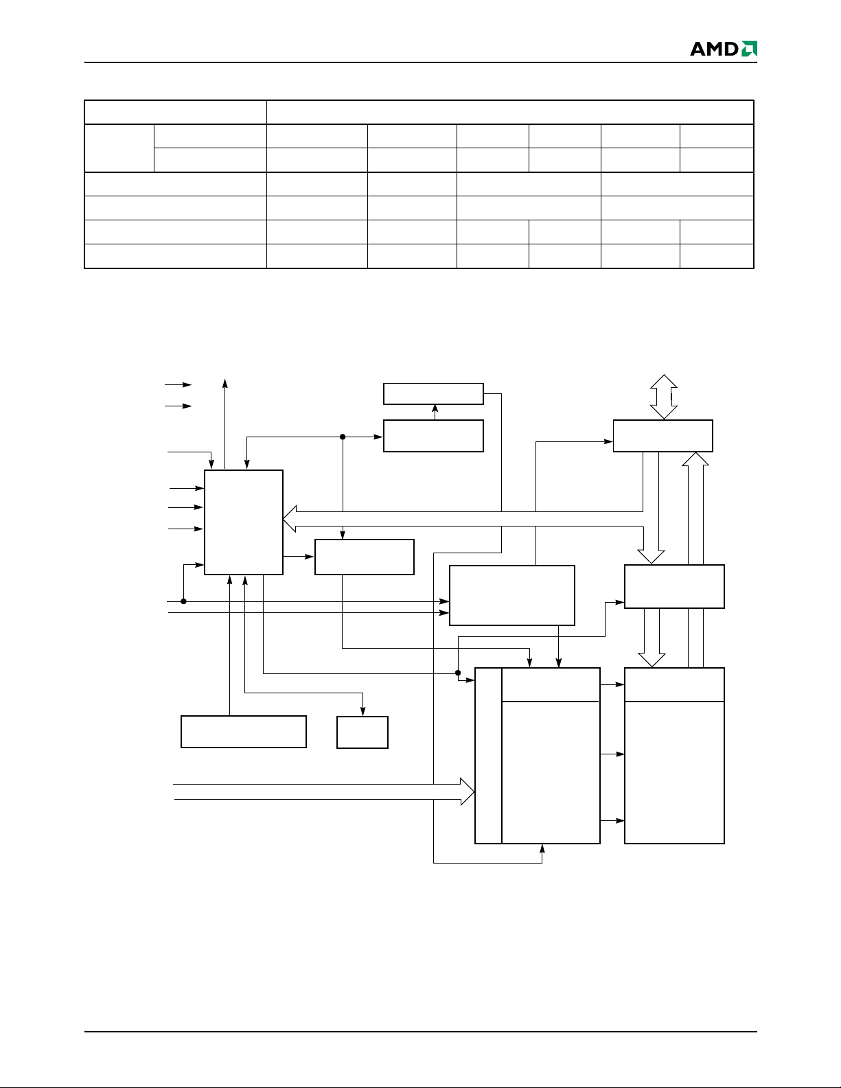
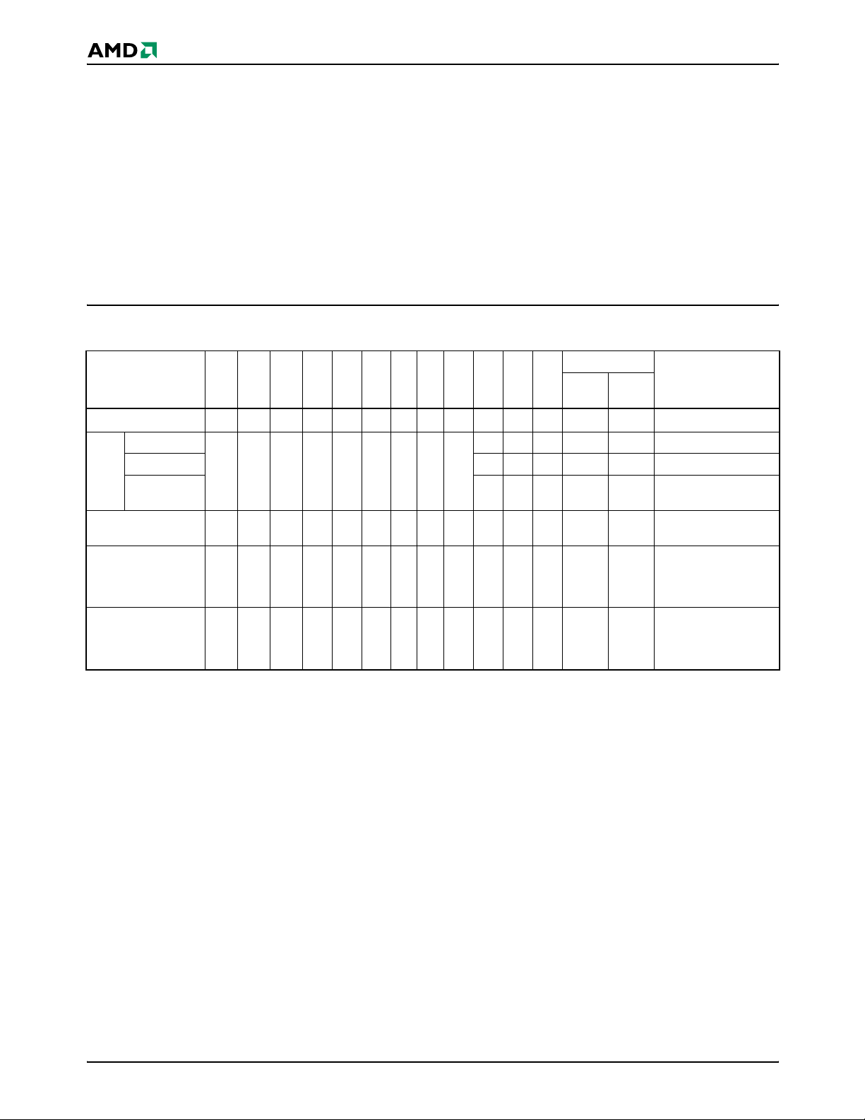
MIRRORBIT 32 MBIT DEVICE FAMILY
Device Bus Sector Architecture Packages VIORY/BY# WP#, ACC WP# Protection
LV033MU x8 Uniform (64 Kbyte)
LV320MT/B x8/x16
LV320MH/L x8/x16 Uniform (64 Kbyte)
Boot (8 x 8 Kbyte
at top & bottom)
40-pin TSOP (std. & rev. pinout),
48-ball FBGA
48-pin TSOP, 48-ball Fine-pitch BGA,
64-ball Fortified BGA
56-pin TSOP (std. & rev. pinout),
64-ball Fortified BGA
Yes Yes ACC only No WP#
No Ye s WP#/ACC pin
Yes Yes WP#/ACC pin
2 x 8 Kbyte
top or bottom
1 x 64 Kbyte
high or low
RELATED DOCUMENTS
To download related documents, click on the following
links or go to www.amd.com
uct Information
→MirrorBit→Flash Information→Tech-
→Flash Memory→Prod-
nical Documentation.
MirrorBit™ Flash Memory Write Buffer Programming
and Page Buffer Read
Implementing a Commo n Layout for AMD Mi rrorBit
and Intel StrataFlash Memory Devices
Migrating from Single-byte to Three-byte Device IDs
AMD MirrorBit™ White Paper
May 16, 2003 Am29LV320MT/B 3
Page 4

DATASHEET
TABLE OF CONTENTS
Product Selector Guide. . . . . . . . . . . . . . . . . . . . . 5
Block Diag ra m . . . . . . . . . . . . . . . . . . . . . . . . . . . . 5
Connection Diagrams . . . . . . . . . . . . . . . . . . . . . . 6
Pin Description. . . . . . . . . . . . . . . . . . . . . . . . . . . . 8
Ordering Information. . . . . . . . . . . . . . . . . . . . . . . 9
Device Bus Operations . . . . . . . . . . . . . . . . . . . . 10
Table 1. Device Bus Operation s ....................... ............................ ..10
Requirements for Reading Array Data ........................ ...........10
Writing Commands/Command Sequences ............................11
Automatic Sleep Mode ................. ............ ............ ..................12
RESET#: Hardware Reset Pi n ................................. ..............12
Output Disable Mode ..............................................................12
Table 2. Am29LV320MT Top Boot Sector Architecture ..................12
Table 3. Am29LV320MB Bottom Boot Sector Architecture .............14
Table 4. Autoselect Codes, (High Voltage Method) .......................16
Sector Group Protection and Unprotection .............................17
Table 5. Am29LV320MT Top Boot Sector Protection .....................17
Table 6. Am29LV320MB Bottom Boot Sector Protection ................17
Write Protect (WP#) ................................................................17
Temporary Sector Group Unprotect ....................................... 18
Figure 1. Temporary Sector Group Unprotect Operation................ 18
Figure 2. In-System Sector Group Protect/Unprotect A lgorit hm s ... 19
SecSi (Secured Silicon) Sector Flash Memory Region ..........20
Table 7. SecSi Sector Contents ......................................................20
Figure 3. SecSi Sector Protect Verify.............................................. 21
Hardware Data Protection ......................................................21
Common Flash Memory Interface (CFI). . . . . . . 21
Command Definitions . . . . . . . . . . . . . . . . . . . . . 24
Reading Array Data ................................................................24
Reset Command ................. .................................. ............ ......25
Autoselect Command Sequence ............................................25
Enter SecSi Sector/Exit SecSi Sector CommandSequence ..25
Word/Byte Program Command Sequence .............................25
Figure 4. Write Buffer Programming Operation............................... 28
Figure 5. Program Operation............................................. ............. 29
Program Suspend/Program Resume Command Sequence ...29
Figure 6. Program Suspend/Program Resume............................... 30
Chip Erase Command Sequence ...........................................30
Sector Erase Command Sequence ........................................30
Figure 7. Erase Operation............................................................... 31
Erase Suspend/Erase Resume Commands ................ ...........31
Write Operation Status . . . . . . . . . . . . . . . . . . . . 34
DQ7: Data# Polling ................................................................. 34
Figure 8. Data# Polling Algorithm ................................................... 34
DQ6: Toggle Bit I ....................................................................35
Figure 9. Toggle Bit Algorithm......................................................... 36
DQ2: Toggle Bit II ...................................................................36
Reading Toggle Bits DQ6/DQ2 ..............................................36
DQ5: Exceeded Timing Limits ................................................ 37
DQ3: Sector Era s e Time r ..................... ... .. .............. ... .. ..........37
DQ1: Write-to-B u ffer A b o rt .................................. .. .. ... ............37
Table 14. Write Operation Sta tus ........................ .............. .............37
Absolute Maximum Ratings. . . . . . . . . . . . . . . . . 38
Figure 10. Maximum Negative Overshoot Waveform................... 38
Figure 11. Maximum Positive Overshoot Waveform..................... 38
DC Characteristics . . . . . . . . . . . . . . . . . . . . . . . . 39
Test Conditions. . . . . . . . . . . . . . . . . . . . . . . . . . . 40
Figure 12. Test Setup..... ............................ ............................ ....... 40
Table 15. Test Specifications ............................................ .............40
Key to Switching Waveforms. . . . . . . . . . . . . . . . 40
Figure 13. Input Waveforms and
Measurement Levels...................................................................... 40
AC Characteristics . . . . . . . . . . . . . . . . . . . . . . . . 41
Read-Only Operations ...........................................................41
Figure 14. Read Operation Timings. . .............. ....................... ........ 41
Figure 15. Page Read Timings...................................................... 42
Hardware Reset (RESET#) ....................................................43
Figure 16. Reset Timings............................................................... 43
Erase and Program Operations .............................................. 44
Figure 17. Program Operation Timings.......................................... 45
Figure 18. Accelerated Program Timing Diagram.......................... 45
Figure 19. Chip/Sector Erase Operation Timings.......................... 46
Figure 20. Data# Polling Timings (During Embedded Algorithms). 47
Figure 21. Toggle Bit Timings (During Embedded Algorithms)...... 48
Figure 22. DQ2 vs. DQ6......................... ........................................ 48
Temporary Sector Unprotect ..................................................49
Figure 23. Temporary Sector Group Unprotect Timing Dia gram ... 49
Figure 24. Sector Group Protect and Unprotect Timing Diagram .. 50
Alternate CE# Controlled Erase and ProgramOperations .....51
Figure 25. Alternate CE# Controlled Write (Erase/Program)
OperationTimings....................... .............. ........................... .......... 52
Erase And Programming Performan ce. . . . . . . . 53
Latchup Characteristics. . . . . . . . . . . . . . . . . . . . 53
TSOP Pin and BGA Package Capacitance . . . . . 54
Data Retention. . . . . . . . . . . . . . . . . . . . . . . . . . . . 54
Physical Dimensions . . . . . . . . . . . . . . . . . . . . . . 55
TS 048—48-Pin Standard Pinout Thin Small Outline Package
(TSOP) ................................................................................... 55
Physical Dimensions . . . . . . . . . . . . . . . . . . . . . . 56
TS 048—48-Pin Standard Pinout Thin Small Outline Package
(TSOP) ................................................................................... 56
FBC048—48-Ball Fine-pitch Ball Grid Array (fBGA)
9 x 8 mm P ackage ........... ................... ..................... ............... 5 7
Physical Dimensions
LAA064—64-Ball Fortified Ball Grid Array (FBGA)
13 x 11 mm Package. . . . . . . . . . . . . . . . . . . . . . . 58
Revision Summary . . . . . . . . . . . . . . . . . . . . . . . . 60
4 Am29LV320MT/B May 16, 2003
Page 5
DATASHEET
PRODUCT SELECTOR GUIDE
Part Number Am29LV320MT/B
V
= 3.0–3.6 V 90R 100R 110R 120R
Speed
Option
Max. Access Time (ns) 90 100 110 120
Max. CE# Access Time (ns) 90 100 110 120
CC
V
= 2.7–3.6 V 100 110 120
CC
Max. Page access time (t
)25 30 30403040
PACC
Max. OE# Access Time (ns) 25 30 30 40 30 40
Note: See “AC Characteristics” for full specifications.
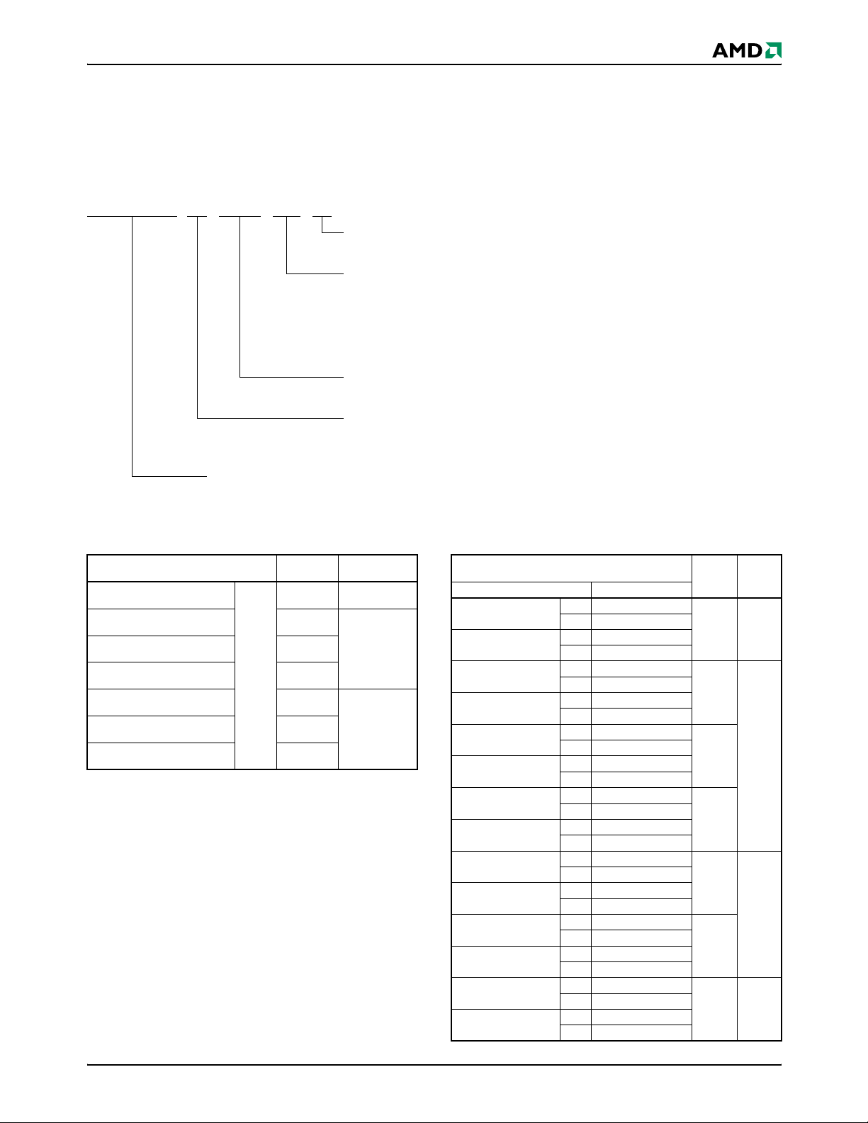
BLOCK DIAGRAM
DQ0
–DQ15 (A-1)
Input/Output
Buffers
Data
Latch
V
CC
V
RESET#
WE#
WP#/ACC
BYTE#
CE#
OE#
RY/BY#
Sector Switches
SS
Erase Voltage
Generator
State
Control
Command
Register
PGM Voltage
Generator
Chip Enable
Output Enable
STB
Logic
A20–A0
VCC Detector
Timer
STB
Y-Decoder
X-Decoder
Address Latch
Y-Gating
Cell Matrix
May 16, 2003 Am29LV320MT/B 5
Page 6
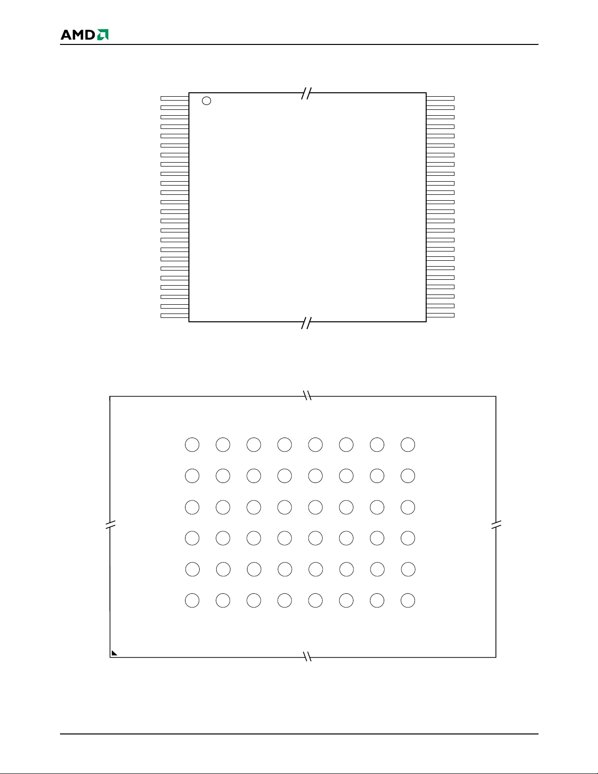
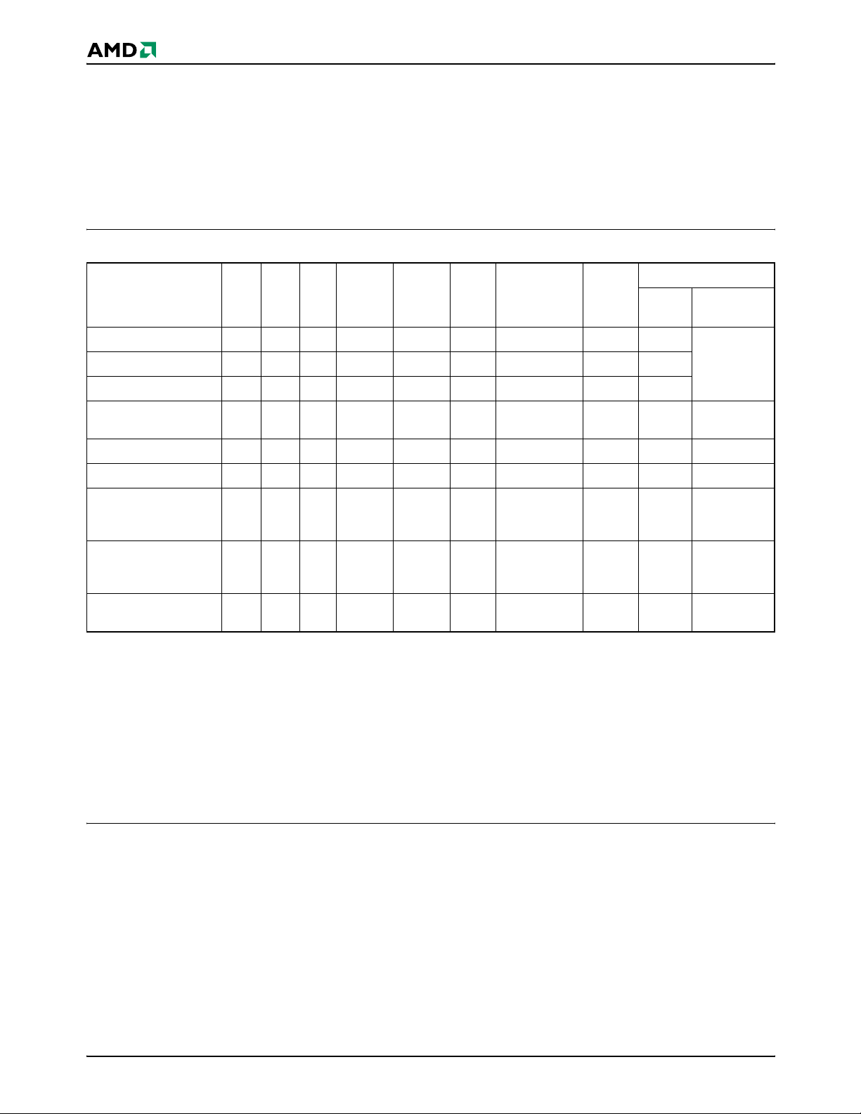
CONNECTION DIAGRAMS
DATASHEET
A15
A14
A13
A12
A11
A10
A9
A8
A19
A20
WE#
RESET#
NC
WP#/ACC
RY/BY#
A18
A17
A7
A6
A5
A4
A3
A2
A1
1
2
3
4
5
6
7
8
9
10
11
12
13
14
15
16
17
18
19
20
21
22
23
24
48-Pin Standard TSOP
48
47
46
45
44
43
42
41
40
39
38
37
36
35
34
33
32
31
30
29
28
27
26
25
A16
BYTE#
V
SS
DQ15/A-1
DQ7
DQ14
DQ6
DQ13
DQ5
DQ12
DQ4
V
CC
DQ11
DQ3
DQ10
DQ2
DQ9
DQ1
DQ8
DQ0
OE#
V
SS
CE#
A0
48-ball Fine-pitch BGA
Top View, Balls Facing Down
A6 B6 C6 D6 E6 F6 G6 H6
DQ15/A-1
A5 B5 C5 D5 E5 F5 G5 H5
DQ13 DQ6DQ14DQ7A11A10A8A9
A4 B4 C4 D4 E4 F4 G4 H4
V
A3 B3 C3 D3 E3 F3 G3 H3
DQ11 DQ3DQ10DQ2A20A18WP#/ACCRY/BY#
A2 B2 C2 D2 E2 F2 G2 H2
DQ9 DQ1DQ8DQ0A5A6A17A7
A1 B1 C1 D1 E1 F1 G1 H1
OE#
V
CC DQ4DQ12DQ5A19NCRESET#WE#
V
SSBYTE#A16A15A14A12A13
SSCE#A0A1A2A4A3
6 Am29LV320MT/B May 16, 2003
Page 7
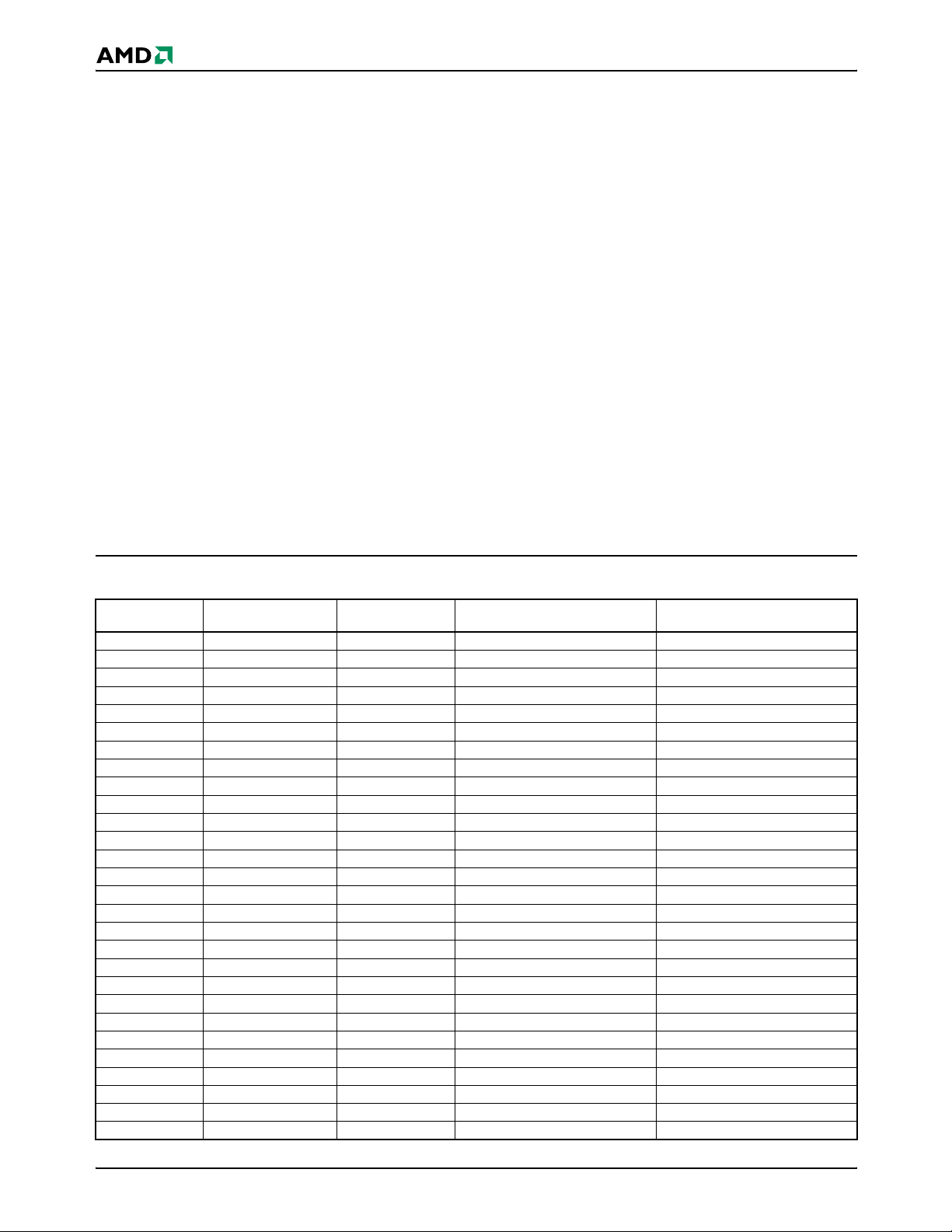
CONNECTION DIAGRAMS
DATASHEET
64-Ball Fortified BGA
Top View, Balls Facing Down
A8
NC
A7
A13
A6
A9
A5
WE#
A4
RY/BY#
A3
A7
A2
A3
A1
NC
B8 C8 D8 E8 F8 G8 H8
NCNCNC
B7 C7 D7 E7 F7 G7 H7
B6 C6 D6 E6 F6 G6 H6
B5 C5 D5 E5 F5 G5 H5
B4 C4 D4 E4 F4 G4 H4
B3 C3 D3 E3 F3 G3 H3
B2 C2 D2 E2 F2 G2 H2
B1 C1 D1 E1 F1 G1 H1
SS
DQ15/A-1BYTE#A16A15A14A12
DQ13DQ14DQ7A11A10A8
DQ12DQ5A19NCRESET#
CC
OE#CE#A0A1A2A4
NCNCNCV
V
SS
DQ6
DQ4V
DQ3DQ11DQ10DQ2A20A18WP#/ACC
DQ1DQ9DQ8DQ0A5A6A17
V
SS
NCNCNCNCNCNCNC
Special Package Handling Instructions
and/or data integrity may be compromi sed if the
package body is exposed to temperatures above 150°C
Special handling is required for Flash Memory products
for prolonged periods of time.
in molded packages (TSOP and BGA). The package
May 16, 2003 Am29LV320MT/B 7
Page 8
DATASHEET
PIN DESCRIPTION
A20–A0 = 21 Address inputs
DQ14–DQ0 = 15 Data inputs/outputs
DQ15/A-1 = DQ15 (Data input/output, word mode),
A-1 (LSB Address input, byte mode)
CE# = Chip Enable input
OE# = Output Enable input
WE# = Write Enable input
WP#/ACC = Hardware Write Protect input/Pro-
gramming Acceleration input
RESET# = Hardware Reset Pin input
RY/BY# = Ready/Busy output
BYTE# = Selects 8-bit or 16-bit mode
= 3.0 volt-only single power supply
V
CC
V
SS
NC = Pin Not Connected Internally
(see Product Selector Guide for
speed options and voltage
supply tolerances)
= Device Ground
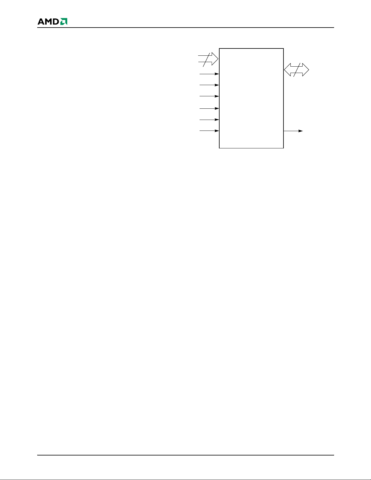
LOGIC SYMBOL
21
A20–A0
CE#
OE#
WE#
WP#/ACC
RESET#
BYTE#
16 or 8
DQ15–DQ0
(A-1)
RY/BY#
8 Am29LV320MT/B May 16, 2003
Page 9
DATASHEET
ORDERING INFORMATION
Standard Products
AMD standard products are available in several packages and operating ranges. The order number (Valid Combination) is
formed by a combination of the following:
Am29LV320M T 120R PC I
TEMPERATURE RANGE
I = Industrial (–40
PACKAGE TYPE
E = 48-Pin Thin Small Outline Package (TSOP) Standard Pinout (TS 048)
PC = 64-Ball Fortified Ball Grid Array (
1.0 mm pitch, 13 x 11 mm package (LAA064)
WC = 48-Ball Fine Pitch Ball Grid Array (FBGA),
0.80 mm pitch, 9 x 8 mm package (FBC048)
SPEED OPTION
See Product Selector Guide a nd Valid Combinations
°C to +85°C)
FBGA),
SECTOR ARCHITECTURE AND WP# PROTECTION (WP# = V
T = Top boot sector device, top two address secto rs protected
B = Bottom boot sector device, bottom two address sectors protected
DEVICE NUMBER/DESCRIPTION
Am29LV320MT/B
32 Megabit (2 M x 16-Bit/4 M x 8-Bit) MirrorBit Boot Sector Flash Memory
3.0 Volt-only Read, Program, and Erase
Valid Combinations for
TSOP Package
Am29LV320MT90R,
Am29LV320MB90R
Am29LV320MT100,
Am29LV320MB100
Am29LV320MT110,
Am29LV320MB110
Am29LV320MT120,
Am29LV320MB120
Am29LV320MT100R,
Am29LV320MB100R
Am29LV320MT110R,
Am29LV320MB110R
Am29LV320MT120R,
Am29LV320MB120R
Speed
(ns)
90 3.0–3.6 V
100
110
EI
120
100
110
120
V
CC
Range
2.7–3.6 V
3.0–3.6 V
Valid Combinations
Valid Com binations l ist c onfi gurations pl anned to be supported in volume for this device. Consult the local AMD sales office to confirm
availability of specific valid combinations and to check on newly released combinations.
Valid Combinations for
BGA Packages
Order Number Package Markin g
Am29LV320MT90R
Am29LV320MB90R
Am29LV320MT100
Am29LV320MB100
Am29LV320MT110
Am29LV320MB110
Am29LV320MT120
Am29LV320MB120
Am29LV320MT100R
Am29LV320MB100R
Am29LV320MT110R
Am29LV320MB110R
Am29LV320MT120R
Am29LV320MB120R
WCI L320MT90QI
PCI L320MT90NI
WCI L320MB90QI
PCI L320MB10NI
WCI L320MT10UI
PCI L320MT10PI
WCI L320MB10UI
PCI L320MB10PI
WCI L320MT11UI
PCI L320MT11PI
WCI L320MB11UI
PCI L320MB11PI
WCI L320MT12UI
PCI L320MT12PI
WCI L320MB12UI
PCI L320MB12PI
WCI L320MT10QI
PCI L320MT10NI
WCI L320MB10QI
PCI L320MB10NI
WCI L320MT11QI
PCI L320MT11NI
WCI L320MB11QI
PCI L320MB11NI
WCI L320MT12QI
PCI L320MT12NI
WCI L320MB12QI
PCI L320MB12NI
IL
)
Speed
(ns)
90
100
110
120
100
110
120
V
CC
Range
3.0–
3.6 V
2.7–
3.6 V
3.0–
3.6 V
3.0–
3.6 V
May 16, 2003 Am29LV320MT/B 9
Page 10
DATASHEET
DEVICE BUS OPERATIONS
This section describes the requirements and use of
the device bus operations, which are in itiated through
the internal command register. The command register
itself does not occupy any addressabl e memory l ocation. The register is a latch used to store the commands, along with the ad dress and da ta information
needed to execute the command. The contents of the
Table 1. Device Bus Operations
register serve as inputs to the intern al state machine.
The state machine outputs dictate the function of the
device. Table 1 lists the device bus operations, the in-
puts and control l evels they requir e, and the resultin g
output. The following subsections de scribe each of
these operations in further detail.
DQ8–DQ15
Addresses
Operation CE# OE# WE# RESET# WP# ACC
Read L L H H
Write (Program/Erase) L H L H (Note 3) X A
Accelerated Program L H L H
±
V
Standby
Output Disable L H H H
Reset X X X L
Sector Group Protect
(Note 2)
Sector Group Unprotect
(Note 2)
T emporary Sector Group
Unprotect
CC
0.3 V
XX
LHL V
LHL V
XXX V
V
CC
0.3 V
ID
ID
ID
±
XX
(Note 3) V
HH
XH
XX
XX
HX
HX
HX A
(Note 2)
SA, A6 =L,
A3=L, A2=L,
A1=H, A0=L
SA, A6=H,
A3=L, A2=L,
A1=H, A0=L
DQ0–
DQ7
A
IN
IN
A
IN
X
X
X
D
(Note 4) (Note 4)
(Note 4) (Note 4)
High-Z High-Z High-Z
High-Z High-Z High-Z
High-Z High-Z High-Z
(Note 4) X X
(Note 4) X X
IN
(Note 4) (Note 4) High-Z
OUT
BYTE#
= V
IH
D
OUT
BYTE#
= V
IL
DQ8–DQ14
= High-Z,
DQ15 = A-1
Legend: L = Logic Low = VIL, H = Logic Hi gh = VIH, VID = 11.5–12.5 V, VHH = 11.5–12. 5 V , X = Do n’t Care , SA = Sect or Addr ess ,
= Address In, DIN = Data In, D
A
IN
= Data Out
OUT
Notes:
1. Addresses are A20:A0 in word mode; A20:A-1 in byte mode. Sector addresses are A20:A12 in both modes.
2. The sector protect and sector unprotect functions may al so be i mplemente d via programmi ng equipmen t. See the “Sector Group
Protection and Unprotection” sectio n.
3. If WP# = V
, the first or last sector remains protect ed. I f WP# = VIH, the top two or bottom two sectors wi ll be prot ected or
IL
unprotected as determined by the method d escribe d in “Sector Group Pr otecti on and Unprotect ion ”. All sector s are unprote cted
when shipped from the factory (The SecSi Secto r may be facto ry pr otected depending on ver sion or dered.)
4. D
IN
or D
as required by command sequence, data polling, or sector protect algorithm (see Figure 2).
OUT
Word/Byte Configuration
The BYTE# pin controls whether the de vice data I/O
pins operate in the b yte or word confi guration. If the
BYTE# pin is set at logic ‘1’, the device is in word configuration, DQ0–DQ15 are active and co ntrolled by
CE# and OE#.
If the BYTE# pin is set at logic ‘0’, the device is in byte
configuration, and only data I/O pins DQ0–DQ7 are
active and controlled by CE# and OE#. The data I/O
pins DQ8–DQ14 are tri-stated, and the DQ15 pin is
used as an input for the LSB (A-1) address function.
Requirements for Reading Array Data
To read array data from the outputs, the system must
drive the CE# and OE# pins to V
control and selects the device. OE# is the output control and gates array data to the output pins. WE#
should remain at V
.
IH
. CE# is the power
IL
10 Am29LV320MT/B May 16, 2003
Page 11

DATASHEET
The internal state machine is set for reading array data
upon device power-up, or after a hardware reset. This
ensures that no spurious alteration of the memory
content occurs durin g the power transition. No command is necessary in this mode to obtain array data.
Standard microprocessor read cycles that assert valid
addresses on the device address inputs produce valid
data on the device data outputs. The device remains
enabled for read access until the command register
contents are altered.
See “Reading Array Data” for more information. Refer
to the AC Read-Only Operations table for timing spec-
ifications and to Figure 14 for the timing diagram.
Refer to the DC Characteristics table for the active
current specification on reading array data.
Page Mode Read
The device is capable of fast page mode read and is
compatible with the page mode Mask ROM read operation. This mode provides faster read access speed
for random locations wi thin a page. T he page s ize of
the device is 4 words/8 bytes. The appropriate page is
selected by th e higher addres s bits A(ma x)–A2. A ddress bits A1–A0 in word mode (A1–A-1 in byte mode)
determine the specif ic wor d withi n a page. This is an
asynchronous operation; the m icroprocesso r supplies
the specific word location.
The random or initial page access is equal to t
and subsequent page read accesses (as long as
t
CE
ACC
or
the locations specified by the microprocessor falls
within that page) is equival ent to t
. When CE# is
PACC
deasserted and reasserted for a subsequent access,
the access time is t
or tCE. Fast page mode ac-
ACC
cesses are obtained by keeping the “read-page addresses” constant and cha nging the “i ntra-read p age”
addresses.
Writing Commands/Command Sequences
To write a command or command sequence (which includes programming data to the device and erasing
sectors of memory), the system must drive WE# and
CE# to V
The device features an Unlock Bypass mode to facilitate faster programming. Once the device enters the
Unlock Bypass mo de, only two write cycles are required to program a word or byte, instead of four. The
“Word/Byte Program Co mmand Sequenc e” section
has details on programming data to the device using
both standard and Unlock Bypass command sequences.
An erase operation can erase one sector, multiple sectors, or the entire device. Tables 3 and 2 indicates the
address space that each sector occupies.
Refer to the DC Characteristics table for the active
current specification for the write mode. The AC Char-
, and OE# to VIH.
IL
acteristics section contains timing spec ification tables
and timing diagrams for write operations.
Write Buffer
Write Buffer Programming allows the system to write a
maximum of 16 words/32 bytes in one programming
operation. This results in faster effective programming
time than the standard programming algorithms. See
“Write Buffer” for more information.
Accelerated Program Operation
The device offers accelerated program operations
through the ACC function. This is one of two functions
provided by the WP#/ACC pin. This function is primarily intended to allow faster manu facturing throu ghput
at the factory.
If the system asserts V
on this pin, the device auto-
HH
matically enters the aforementioned Unlock Bypass
mode, temporarily unprotects any protec ted sectors,
and uses the higher voltage on the pin to reduce the
time required for program operations. The system
would use a two-cycle progra m command sequence
as required by the Unlock Bypass mode. Removing
from the WP#/ACC p in returns th e device to nor-
V
HH
mal operation. N ote that the WP# /ACC pin must not
be at V
for operations oth er than acceler ated pro-
HH
gramming, or device damage may result. In addition,
no external pullup is necessary since the WP#/ACC
pin has internal pullup to V
CC
.
Autoselect Functions
If the system writes the autoselect command s equence, the device enters the autoselect mo de. The
system can then read autoselect codes from the internal register (which is separate from the memory array)
on DQ7–DQ0. Standard read cycle timings apply in
this mode. Refer to the Autoselect M ode and Au tose-
lect Command Sequence sections for m ore informa-
tion.
Standby Mode
When the system is n ot reading or wri ting to the device, it can place the device in the standby mode. In
this mode, current consum ption is greatly reduc ed,
and the outputs are placed in the high impedance
state, independent of the OE# input.
The device enters the CMOS standby mode when the
CE# and RESET# pins are both held at V
(Note that this is a more restricted voltage range tha n
.) If CE# and RESET# are held at VIH, but not within
V
IH
± 0.3 V, the device will be in the s tandby mode,
V
CC
but the standby current will be greater. The device requires standard ac cess time (t
) for read access
CE
when the device is in either of these standby modes,
before it is ready to read data.
± 0.3 V.
CC
May 16, 2003 Am29LV320MT/B 11
Page 12
DATASHEET
If the device is deselected during erasure or programming, the device draws active current until the
operation is completed.
Refer to the DC Characteristics table for the standby
current specification.
Automatic Sleep Mode
The automatic sleep mode minimizes Flash device energy consumption. The device automatically enables
this mode when addresses remain stable for t
ACC
+
30 ns. The automatic sleep mode is independent of
the CE#, WE#, and OE# control signals. Standard address access timings provide new data when addresses are changed. While in sleep mode, output
data is latched and always available to the system.
Refer to the DC Characteristics table for the automatic
sleep mode current specification.
RESET#: Hardware Reset Pin
The RESET# pin provides a hardware me thod of resetting the device to reading array data. When the RESET# pin is driven low for at least a period of t
device immediately term inates any operation in
progress, tristates all output pins, and ignores all
RP
, the
read/write command s for the dur ation of the RESET#
pulse. The device also resets the internal state machine to reading array data. The operation that was interrupted should be reinitiated once the device is
ready to accept another command sequence, to ensure data integrity.
Current is reduced for the duration of the RESET#
pulse. When RESET# is held at V
draws CMOS standby current (I
but not within VSS±0.3 V, the standby current will
at V
IL
±0.3 V, the device
SS
). If RESET# is held
CC4
be greater.
The RESET# pin may be tied to the system reset cir-
cuitry. A system reset would thus also reset the Flash
memory, enabling the system to read the boot-up firmware from the Flash memory.
Refer to the AC Characteristics tables for RESET# parameters and to Figure 16 for the timing diagram.
Output Disable Mode
When the OE# input is at VIH, output from the device is
disabled. The output pins are placed in the high
impedance state.
Table 2. Am29LV320MT Top Boot Sector Architecture
Sector
SA0 000000xxx 64/32 000000h–00FFFFh 00000h–07FFFh
SA1 000001xxx 64/32 010000h–01FFFFh 08000h–0FFFFh
SA2 000010xxx 64/32 020000h–02FFFFh 10000h–17FFFh
SA3 000011xxx 64/32 030000h–03FFFFh 18000h–1FFFFh
SA4 000100xxx 64/32 040000h–04FFFFh 20000h–27FFFh
SA5 000101xxx 64/32 050000h–05FFFFh 28000h–2FFFFh
SA6 000110xxx 64/32 060000h–06FFFFh 30000h–37FFFh
SA7 000111xxx 64/32 070000h–07FFFFh 38000h–3FFFFh
SA8 001000xxx 64/32 080000h–08FFFFh 40000h–47FFFh
SA9 001001xxx 64/32 090000h–09FFFFh 48000h–4FFFFh
SA10 001010xxx 64/32 0A0000h–0AFFFFh 50000h–57FFFh
SA11 001011xxx 64/32 0B0000h–0BFFFFh 58000h–5FFFFh
SA12 001100xxx 64/32 0C0000h–0CFFFFh 60000h–67FFFh
SA13 001101xxx 64/32 0D0000h–0DFFFFh 68000h–6FFFFh
SA14 001101xxx 64/32 0E0000h–0EFFFFh 70000h–77FFFh
SA15 001111xxx 64/32 0F0000h–0FFFFFh 78000h–7FFFFh
SA16 010000xxx 64/32 100000h–00FFFFh 80000h–87FFFh
SA17 010001xxx 64/32 110000h–11FFFFh 88000h–8FFFFh
SA18 010010xxx 64/32 120000h–12FFFFh 90000h–97FFFh
SA19 010011xxx 64/32 130000h–13FFFFh 98000h–9FFFFh
SA20 010100xxx 64/32 140000h–14FFFFh A0000h–A7FFFh
SA21 010101xxx 64/32 150000h–15FFFFh A8000h–AFFFFh
SA22 010110xxx 64/32 160000h–16FFFFh B0000h–B7FFFh
SA23 010111xxx 64/32 170000h–17FFFFh B8000h–BFFFFh
SA24 011000xxx 64/32 180000h–18FFFFh C0000h–C7FFFh
SA25 011001xxx 64/32 190000h–19FFFFh C8000h–CFFFFh
SA26 011010xxx 64/32 1A0000h–1AFFFFh D0000h–D7FFFh
SA27 011011xxx 64/32 1B0000h–1BFFFFh D8000h–DFFFFh
Sector Address
A20–A12
Sector Size
(Kbytes/Kwords)
(x8)
Address Range
(x16)
Address Range
12 Am29LV320MT/B May 16, 2003
Page 13
DATASHEET
Table 2. Am29LV320MT Top Boot Sector Architecture (Continued)
Sector
SA28 011000xxx 64/32 1C0000h–1CFFFFh E0000h–E7FFFh
SA29 011101xxx 64/32 1D0000h–1DFFFFh E8000h–EFFFFh
SA30 011110xxx 64/32 1E0000h–1EFFFFh F0000h–F7FFFh
SA31 011111xxx 64/32 1F0000h–1FFFFFh F8000h–FFFFFh
SA32 100000xxx 64/32 200000h–20FFFFh F9000h–107FFFh
SA33 100001xxx 64/32 210000h–21FFFFh 108000h–10FFFFh
SA34 100010xxx 64/32 220000h–22FFFFh 110000h–117FFFh
SA35 101011xxx 64/32 230000h–23FFFFh 118000h–11FFFFh
SA36 100100xxx 64/32 240000h–24FFFFh 120000h–127FFFh
SA37 100101xxx 64/32 250000h–25FFFFh 128000h–12FFFFh
SA38 100110xxx 64/32 260000h–26FFFFh 130000h–137FFFh
SA39 100111xxx 64/32 270000h–27FFFFh 138000h–13FFFFh
SA40 101000xxx 64/32 280000h–28FFFFh 140000h–147FFFh
SA41 101001xxx 64/32 290000h–29FFFFh 148000h–14FFFFh
SA42 101010xxx 64/32 2A0000h–2AFFFFh 150000h–157FFFh
SA43 101011xxx 64/32 2B0000h–2BFFFFh 158000h–15FFFFh
SA44 101100xxx 64/32 2C0000h–2CFFFFh 160000h–167FFFh
SA45 101101xxx 64/32 2D0000h–2DFFFFh 168000h–16FFFFh
SA46 101110xxx 64/32 2E0000h–2EFFFFh 170000h–177FFFh
SA47 101111xxx 64/32 2F0000h–2FFFFFh 178000h–17FFFFh
SA48 110000xxx 64/32 300000h–30FFFFh 180000h–187FFFh
SA49 110001xxx 64/32 310000h–31FFFFh 188000h–18FFFFh
SA50 110010xxx 64/32 320000h–32FFFFh 190000h–197FFFh
SA51 110011xxx 64/32 330000h–33FFFFh 198000h–19FFFFh
SA52 100100xxx 64/32 340000h–34FFFFh 1A0000h–1A7FFFh
SA53 110101xxx 64/32 350000h–35FFFFh 1A8000h–1AFFFFh
SA54 110110xxx 64/32 360000h–36FFFFh 1B0000h–1B7FFFh
SA55 110111xxx 64/32 370000h–37FFFFh 1B8000h–1BFFFFh
SA56 111000xxx 64/32 380000h–38FFFFh 1C0000h–1C7FFFh
SA57 111001xxx 64/32 390000h–39FFFFh 1C8000h–1CFFFFh
SA58 111010xxx 64/32 3A0000h–3AFFFFh 1D0000h–1D7FFFh
SA59 111011xxx 64/32 3B0000h–3BFFFFh 1D 8000h–1DFFFFh
SA60 111100xxx 64/32 3C0000h–3CFFFFh 1E0000h–1E7FFFh
SA61 111101xxx 64/32 3D0000h–3DFFFFh 1E8000h–1EFFFFh
SA62 111110xxx 64/32 3E0000h–3EFFFFh 1F0000h–1F7FFFh
SA63 111111000 8/4 3F0000h–3F1FFFh 1F8000h–1F8FFFh
SA64 111111001 8/4 3F2000h–3F3FFFh 1F9000h–1F9FFFh
SA65 111111010 8/4 3F4000h–3F5FFFh 1FA000h–1FAFFFh
SA66 111111011 8/4 3F6000h–3F7FFFh 1FB000h–1FBFFFh
SA67 111111100 8/4 3F8000h–3F9FFFh 1FC000h–1FCFFFh
SA68 111111101 8/4 3FA000h–3FBFFFh 1FD000h–1FDFFFh
SA69 111111110 8/4 3FC000h–3FDFFFh 1FE000h–1FEFFFh
SA70 111111111 8/4 3FE000h–3FFFFFh 1FF000h–1FFFFFh
Sector Address
A20–A12
Sector Size
(Kbytes/Kwords)
(x8)
Address Range
(x16)
Address Range
May 16, 2003 Am29LV320MT/B 13
Page 14
DATASHEET
Table 3. Am29LV320MB Bottom Boot Sector Architecture
Sector
SA0 000000000 8/4 000000h–001FFFh 00000h–00FFFh
SA1 000000001 8/4 002000h–003FFFh 01000h–01FFFh
SA2 000000010 8/4 004000h–005FFFh 02000h–02FFFh
SA3 000000011 8/4 006000h–007FFFh 03000h–03FFFh
SA4 000000100 8/4 008000h–009FFFh 04000h–04FFFh
SA5 000000101 8/4 00A000h–00BFFFh 05000h–05FFFh
SA6 000000110 8/4 00C000h–00DFFFh 06000h–06FFFh
SA7 000000111 8/4 00E000h–00FFFFFh 07000h–07FFFh
SA8 000001xxx 64/32 010000h–01FFFFh 08000h–0FFFFh
SA9 000010xxx 64/32 020000h–02FFFFh 10000h–17FFFh
SA10 000011xxx 64/32 030000h–03FFFFh 18000h–1FFFFh
SA11 000100xxx 64/32 040000h–04FFFFh 20000h–27FFFh
SA12 000101xxx 64/32 050000h–05FFFFh 28000h–2FFFFh
SA13 000110xxx 64/32 060000h–06FFFFh 30000h–37FFFh
SA14 000111xxx 64/32 070000h–07FFFFh 38000h–3FFFFh
SA15 001000xxx 64/32 080000h–08FFFFh 40000h–47FFFh
SA16 001001xxx 64/32 090000h–09FFFFh 48000h–4FFFFh
SA17 001010xxx 64/32 0A0000h–0AFFFFh 50000h–57FFFh
SA18 001011xxx 64/32 0B0000h–0BFFFFh 58000h–5FFFFh
SA19 001100xxx 64/32 0C0000h–0CFFFFh 60000h–67FFFh
SA20 001101xxx 64/32 0D0000h–0DFFFFh 68000h–6FFFFh
SA21 001101xxx 64/32 0E0000h–0EFFFFh 70000h–77FFFh
SA22 001111xxx 64/32 0F0000h–0FFFFFh 78000h–7FFFFh
SA23 010000xxx 64/32 100000h–00FFFFh 80000h–87FFFh
SA24 010001xxx 64/32 110000h–11FFFFh 88000h–8FFFFh
SA25 010010xxx 64/32 120000h–12FFFFh 90000h–97FFFh
SA26 010011xxx 64/32 130000h–13FFFFh 98000h–9FFFFh
SA27 010100xxx 64/32 140000h–14FFFFh A0000h–A7FFFh
SA28 010101xxx 64/32 150000h–15FFFFh A8000h–AFFFFh
SA29 010110xxx 64/32 160000h–16FFFFh B0000h–B7FFFh
SA30 010111xxx 64/32 170000h–17FFFFh B8000h–BFFFFh
SA31 011000xxx 64/32 180000h–18FFFFh C0000h–C7FFFh
SA32 011001xxx 64/32 190000h–19FFFFh C8000h–CFFFFh
SA33 011010xxx 64/32 1A0000h–1AFFFFh D0000h–D7FFFh
SA34 011011xxx 64/32 1B0000h–1BFFFFh D8000h–DFFFFh
SA35 011000xxx 64/32 1C0000h–1CFFFFh E0000h–E7FFFh
SA36 011101xxx 64/32 1D0000h–1DFFFFh E8000h–EFFFFh
SA37 011110xxx 64/32 1E0000h–1EFFFFh F0000h–F7FFFh
SA38 011111xxx 64/32 1F0000h–1FFFFFh F8000h–FFFFFh
SA39 100000xxx 64/32 200000h–20FFFFh F9000h–107FFFh
SA40 100001xxx 64/32 210000h–21FFFFh 108000h–10FFFFh
SA41 100010xxx 64/32 220000h–22FFFFh 110000h–117FFFh
SA42 101011xxx 64/32 230000h–23FFFFh 118000h–11FFFFh
SA43 100100xxx 64/32 240000h–24FFFFh 120000h–127FFFh
SA44 100101xxx 64/32 250000h–25FFFFh 128000h–12FFFFh
SA45 100110xxx 64/32 260000h–26FFFFh 130000h–137FFFh
SA46 100111xxx 64/32 270000h–27FFFFh 138000h–13FFFFh
SA47 101000xxx 64/32 280000h–28FFFFh 140000h–147FFFh
SA48 101001xxx 64/32 290000h–29FFFFh 148000h–14FFFFh
SA49 101010xxx 64/32 2A0000h–2AFFFFh 150000h–157FFFh
SA50 101011xxx 64/32 2B0000h–2BFFFFh 158000h–15FFFFh
SA51 101100xxx 64/32 2C0000h–2CFFFFh 160000h–167FFFh
SA52 101101xxx 64/32 2D0000h–2DFFFFh 168000h–16FFFFh
SA53 101110xxx 64/32 2E0000h–2EFFFFh 170000h–177FFFh
Sector Address
A20–A12
Sector Size
(Kbytes/Kwords)
(x8)
Address Range
(x16)
Address Range
14 Am29LV320MT/B May 16, 2003
Page 15
DATASHEET
Table 3. Am29LV320MB Bottom Boot Sector Architecture (Continued)
Sector
SA54 101111xxx 64/32 2F0000h–2FFFFFh 178000h–17FFFFh
SA55 110000xxx 64/32 300000h–30FFFFh 180000h–187FFFh
SA56 110001xxx 64/32 310000h–31FFFFh 188000h–18FFFFh
SA57 110010xxx 64/32 320000h–32FFFFh 190000h–197FFFh
SA58 110011xxx 64/32 330000h–33FFFFh 198000h–19FFFFh
SA59 100100xxx 64/32 340000h–34FFFFh 1A0000h–1A7FFFh
SA60 110101xxx 64/32 350000h–35FFFFh 1A8000h–1AFFFFh
SA61 110110xxx 64/32 360000h–36FFFFh 1B0000h–1B7FFFh
SA62 110111xxx 64/32 370000h–37FFFFh 1B8000h–1BFFFFh
SA63 111000xxx 64/32 380000h–38FFFFh 1C0000h–1C7FFFh
SA64 111001xxx 64/32 390000h–39FFFFh 1C8000h–1CFFFFh
SA65 111010xxx 64/32 3A0000h–3AFFFFh 1D0000h–1D7FFFh
SA66 111011xxx 64/32 3B0000h–3BFFFFh 1D 8000h–1DFFFFh
SA67 111100xxx 64/32 3C0000h–3CFFFFh 1E0000h–1E7FFFh
SA68 111101xxx 64/32 3D0000h–3DFFFFh 1E8000h–1EFFFFh
SA69 111110xxx 64/32 3E0000h–3EFFFFh 1F0000h–1F7FFFh
SA70 111111xxx 64/32 3F0000h–3FFFFFh 1F8000h–1FFFFFh
Sector Address
A20–A12
Note: The address range is A20:A-1 in byte mode (BYTE# = VIL) or A20:A0 in word mode (BYTE# = VIH)
Sector Size
(Kbytes/Kwords)
(x8)
Address Range
Address Range
(x16)
May 16, 2003 Am29LV320MT/B 15
Page 16
DATASHEET
Autoselect Mode
The autoselect mode provides manufacturer and device identification, and sector protection verification,
through identifier codes output on DQ7–DQ0. This
mode is prim arily intend ed for progr amming equi pment to automatically match a device to be programmed with its corresponding programming
algorithm. However, the autoselect codes can also be
accessed in-system through the command register .
When using programming equipment, the autoselect
mode requires V
A6, A3, A2, A1, and A0 must be as shown in Table 4.
on address pin A9. Address pins
ID
In addition, when verifying sector protection, the sector
address must appear on the appropriate highest order
address bits (see Tables 2 and 3). Table 4 shows the
remaining address bits that are do n’t care. W hen all
necessary bits have been set as required, the programming equipment may then read the corresponding identifier code on DQ7–DQ0.
To access the autoselect codes in-system, the host
system can issue the autoselect command via the
command register, as shown in Tables 12 and 13. This
method does not require V
. Refer to t he Aut os ele ct
ID
Command Sequence section for more information.
Tabl e 4. Autoselect Codes, (High Voltage Method)
A21
Description CE# OE# WE#
Manufacturer ID: AMD L L H X X
Cycle 1
Cycle 2 H H L 22 X 1Ah
Device ID
Cycle 3 H H H 22 X
Sector Protection
Verification
SecSi Sector In d i cator
Bit (DQ7), WP#
protects top two
address sector
SecSi Sector Indicator
Bit (DQ7), WP#
protects bottom two
address sector
LLHXX
LLHSAX
LLHXX
LLHXX
to
A15
A14
to
A9A8toA7A6A5to
A10
V
ID
V
ID
V
ID
V
ID
V
ID
XLX L L L 00 X 01h
XLX
XLX L H L X X
XLX L HH X X
XLX L HH X X
A3
toA2A1 A0
A4
LLH 22 X 7Eh
DQ8 to DQ15
BYTE#
= V
BYTE#
IH
= V
DQ7 to DQ0
IL
00 (bottom boot)
01h (top boot)
01h (protected),
00h (unprotected)
98h (factory locked),
18h (not factory locked)
88h (factory locked),
08h (not factory locked)
Legend: L = Logic Low = VIL, H = Logic High = VIH, SA = Sector Address, X = Don’t care.
16 Am29LV320MT/B May 16, 2003
Page 17
DATASHEET
Sector Group Protection and
Unprotection
The hardware sector group protection feature disables
both program and erase operations in any sector
group. In this device, a sector group consists of fou r
adjacent sectors that are protected or unprotected at
the same time (see Tables 5 and 6). The hardware
sector group unprotection feature re-enables both program and erase operations in previously protected
sector groups. Sector group protection/unprotection
can be implemented via two methods.
Sector protection/unprotection requires V
SET# pin only, and can be implemented either in-system or via progr amming eq uipment. Figure 2 sh ows
the algorithms and Figure 24 shows the timing diagram. This method uses standard microprocessor bus
cycle timing. For sector group unprotect, all unprotected sector groups must first be protected prior to
the first sector group unprotect write cycle.
The device is shipped with all se ctor groups unprotected. AMD offers the option of programming and
protecting sector groups at its factory prior to shipping
the device through AMD’s ExpressFlash™ Service.
Contact an AMD representative for details.
It is possible to determin e whether a se ctor group is
protected or unprotected. See the Autoselect Mode
section for details.
Table 5. Am29LV320MT Top Boot
Sector Protection
Sector A20–A12
SA0-SA3 0000XXXXXh 256 (4x64) Kbytes
SA4-SA7 0001XXXXXh 256 (4x64) Kbytes
SA8-SA11 0010XXXXXh 256 (4x64) Kbytes
SA12-SA15 0011XXXXXh 256 (4x64) Kbytes
SA16-SA19 0100XXXXXh 256 (4x64) Kbytes
SA20-SA23 0101XXXXXh 256 (4x64) Kbytes
SA24-SA27 0110XXXXXh 256 (4x64) Kbytes
SA28-SA31 0111XXXXXh 256 (4x64) Kbytes
SA32–SA35 1000XXXXXh, 256 (4x64) Kbytes
SA36–SA39 1001XXXXXh 256 (4x64) Kbytes
SA40–SA43 1010XXXXXh 256 (4x64) Kbytes
SA44–SA47 1011XXXXXh 256 (4x64) Kbytes
SA48–SA51 1100XXXXXh 256 (4x64) Kbytes
SA52-SA55 1101XXXXXh 256 (4x64) Kbytes
SA56-SA59 1110XXXXXh 256 (4x64) Kbytes
SA60-SA62
SA63 111111000h 8 Kbytes
SA64 111111001h 8 Kbytes
SA65 111111010h 8 Kbytes
111100XXXh
111101XXXh
111110XXXh
on the RE-
ID
Sector/
Sector Block Size
192 (3x64) Kbytes
Sector A20–A12
SA66 111111011h 8 Kbytes
SA67 111111100h 8 Kbytes
SA68 111111101h 8 Kbytes
SA69 111111110h 8 Kbytes
SA70 111111111h 8 Kbytes
Sector/
Sector Block Size
Table 6. Am29LV320MB Bottom Boot
Sector Protection
Sector A20–A12
SA0 000000000h 8 Kbytes
SA1 000000001h 8 Kbytes
SA2 000000010h 8 Kbytes
SA3 000000011h 8 Kbytes
SA4 000000100h 8 Kbytes
SA5 000000101h 8 Kbytes
SA6 000000110h 8 Kbytes
SA7 000000111h 8 Kbytes
SA8–SA10
SA11–SA14 0001XXXXXh 256 (4x64) Kbytes
SA15–SA18 0010XXXXXh 256 (4x64) Kbytes
SA19–SA22 0011XXXXXh 256 (4x64) Kbytes
SA23–SA26 0100XXXXXh 256 (4x64) Kbytes
SA27-SA30 0101XXXXXh 256 (4x64) Kbytes
SA31-SA34 0110XXXXXh 256 (4x64) Kbytes
SA35-SA38 0111XXXXXh 256 (4x64) Kbytes
SA39-SA42 1000XXXXXh 256 (4x64) Kbytes
SA43-SA46 1001XXXXXh 256 (4x64) Kbytes
SA47-SA50 1010XXXXXh 256 (4x64) Kbytes
SA51-SA54 1011XXXXXh 256 (4x64) Kbytes
SA55–SA58 1100XXXXXh 256 (4x64) Kbytes
SA59–SA62 1101XXXXXh 256 (4x64) Kbytes
SA63–SA66 1110XXXXXh 256 (4x64) Kbytes
SA67–SA70 1111XXXXXh 256 (4x64) Kbytes
000001XXXh,
000010XXXh,
000011XXXh,
Sector/
Sector Block Size
192 (3x64) Kbytes
Write Protect (WP#)
The Write Protect function provides a hardware
method of protecting the top two or bottom two sectors
without using V
vided by the WP#/ACC input.
If the system asserts V
vice disables pro gram a nd er ase func tions in th e first
or last sector independently of whether those sectors
were protected or unprotected usin g the method described in “Sector Group Protecti on and Unprotec ti on”.
Note that if WP#/ACC is at V
the standby mode, the m aximum input lo ad current is
increased. See the table in “DC Characteristics”.
. WP# is one of two functions pro-
ID
on the WP#/ACC pin, the de-
IL
when the device is in
IL
May 16, 2003 Am29LV320MT/B 17
Page 18
DATASHEET
If the system asserts V
on the WP#/ACC pin, the de-
IH
vice reverts to whether the top or bottom two sectors
were previously set to be protected or unprotected
using the method described in “Sector Group Protection and Unprotection”. Note: No external pullup is
necessary since the WP#/ACC pin has internal pullup
to V
CC
Temporary Sector Group Unprotect
(Note: In this device, a sector group consists of four adjacent
sectors that are prote cted or unprotected at the same ti me
(see Table 6).
This feature allo ws tempora ry unprotecti on of previously protected sector groups to change data in-system. The Sector Group Unprotect mode is act ivated by
setting the RESET# p in to V
merly protected sector groups can be programmed o r
erased by selecting the sector group addresses. Once
is removed from the RESET# pi n, all the prev i-
V
ID
ously protected sector groups are protected again.
Figure 1 shows the algorithm, and Figure 23 shows
the timing diagrams, for this feature.
. During this m ode, for-
ID
START
RESET# = V
(Note 1)
Perform Erase or
Program Operations
RESET# = V
Temporary Sector
Group Unprotect
Completed (Note 2)
Notes:
1. All protected sector groups unprotected (If WP# = V
the first or last sector will remain protected).
2. All previously protect ed sec tor gro ups are prote cte d
once again.
ID
IH
,
IL
Figure 1. T emporary Sector Group
Unprotect Operation
18 Am29LV320MT/B May 16, 2003
Page 19
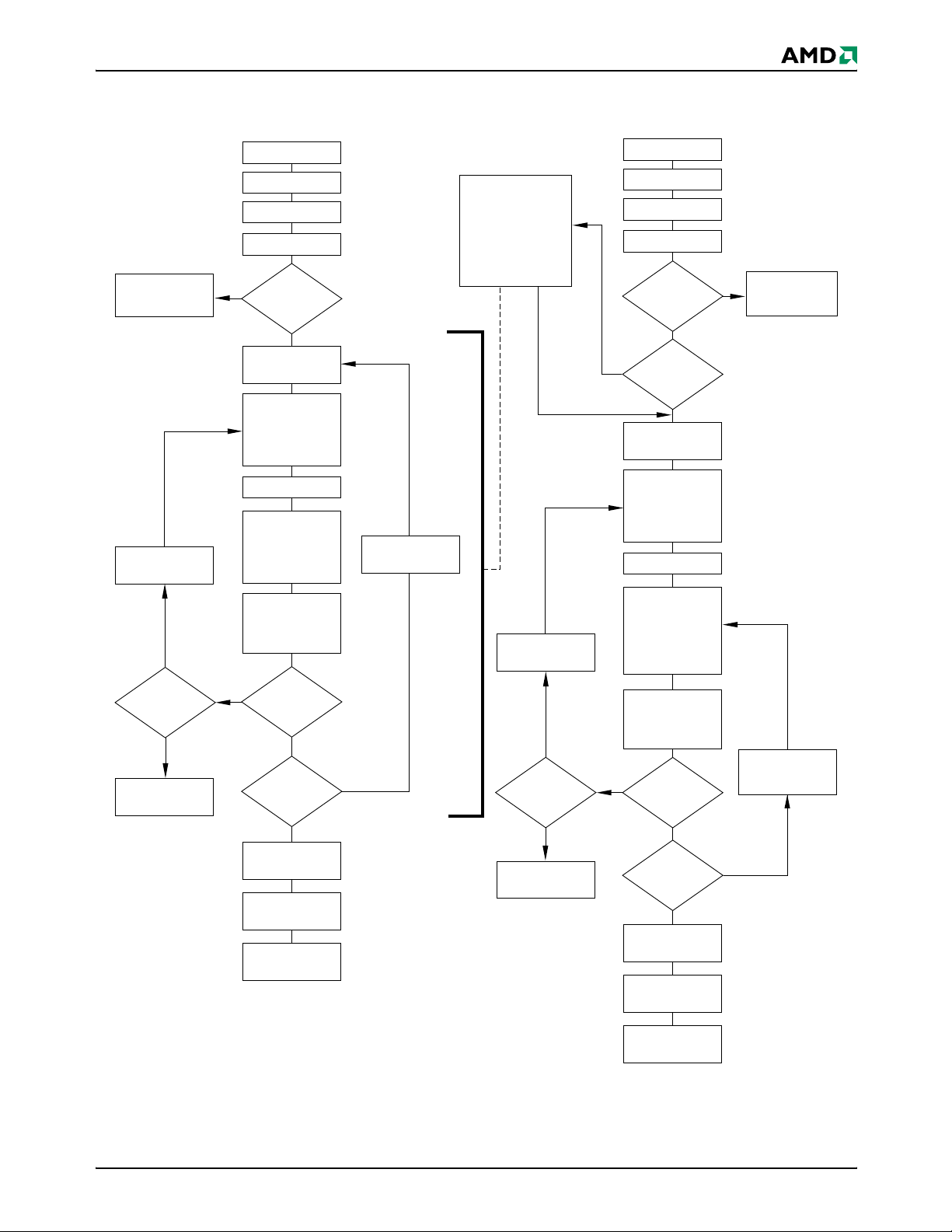
DATASHEET
Temporary Sector
Group Unprotect
Mode
Increment
PLSCNT
START
PLSCNT = 1
RESET# = V
Wait 1 µs
No
First Write
Cycle = 60h?
Set up sector
group address
Sector Group Protect:
Write 60h to sector
group address with
A6–A0 = 0xx0010
Wait 150 µs
Verify Sector Group
Protect: Write 40h
to sector group
address with
A6–A0 = 0xx0010
Yes
START
Protect all sector
groups: The indicated
ID
Reset
PLSCNT = 1
portion of the sector
group protect algorithm
must be performed for all
unprotected sector
groups prior to issuing
the first sector group
unprotect address
PLSCNT = 1
RESET# = V
Wait 1 µs
First Write
Cycle = 60h?
All sector
No
protected?
Set up first sector
group address
Sector Group
Unprotect:
Write 60h to sector
group address with
A6–A0 = 1xx0010
Wait 15 ms
groups
Yes
Yes
ID
Temporary Sector
No
Group Unprotect
Mode
No
PLSCNT
= 25?
Yes
Device failed
Sector Group
Protect
Algorithm
Read from
sector group address
with A6–A0
= 0xx0010
No
Data = 01h?
Protect
another
sector group?
Remove V
from RESET#
Write reset
command
Sector Group
Protect complete
Yes
No
Verify Sector Group
Unprotect: Write
40h to sector group
Increment
PLSCNT
No
Yes
ID
PLSCNT
= 1000?
Yes
Device failed
Sector Group
address with
A6–A0 = 1xx0010
Read from
sector group
address with
A6–A0 = 1xx0010
No
Data = 00h?
Last sector
Remove V
from RESET#
group
verified?
Yes
Yes
ID
Set up
next sector group
address
No
Unprotect
Algorithm
Write reset
command
Sector Group
Unprotect complete
Figure 2. In-System Sector Group Protect/Unprotect Algorithms
May 16, 2003 Am29LV320MT/B 19
Page 20

DATASHEET
SecSi (Secured Silicon) Sector Flash
Memory Region
The SecSi (Secured Silicon) Sector feature provides a
Flash memory region that enables permanent part
identification through an Electronic Serial Number
(ESN). The SecSi Sector is 256 bytes in leng th, and
uses a SecSi Sector Indicator Bit (DQ7) to indicate
whether or not the SecSi Sector is locked when
shipped from the factory. This bit is permanently set at
the factory and cannot be changed, which prevents
cloning of a factory locked part. This ensures the security of the ESN once the product is shipped to the fie ld.
AMD offers the device with the SecSi Sector either
customer lockable (standa rd shipping option) or fac tory locked (contact an AMD sales representative for
ordering information). The customer-lockable version
is shipped with the SecSi Sector unprotected, allowing
customers to program the sector after receiving the
device. The customer-lockable version also has the
SecSi Sector Indicator Bit permanently set to a “0.”
The factory-locked version is always protected when
shipped from the factory, and has the SecSi (Secured
Silicon) Sector Indicator Bit permanently set to a “1.”
Thus, the SecSi Sector Indicator Bit prevents customer-lockable devices from being used to replace devices that are factory locked. Note that the ACC
function and unlock b ypass modes ar e not availabl e
when the SecSi Sector is enabled.
The SecSi sector address space in this device is allocated as follows:
Table 7. SecSi Sector Contents
SecSi Sector
Address Range
000000h–000007h
000008h–00007Fh Unavailable
The system accesses the SecSi Sector through a
command sequence (see “Enter SecSi Sector/Exit
SecSi Sector Command Sequence”). After the system
has written the Enter SecSi Sector command sequence, it may read the SecSi Sector by using the addresses normally occupied by the first sector (SA0).
This mode of operation continues until the system issues the Exit SecSi Sector command sequ ence, or
until power is removed from the device. On power-up,
or following a hardware reset, the device reverts to
sending commands to sector SA0.
Customer
Lockable
Determine d by
customer
ESN Factory
Locked
ESN
ExpressFlash
Factory Locked
ESN or
determined by
customer
Determined by
customer
Customer Lockable: SecSi Sector NOT
Programmed or Protected At the Factory
Unless otherwise specified, the device is shipped such
that the customer may prog ram and protect the
256-byte SecSi sector.
The system may program the SecSi Sector using the
write-buffer, accelerated and/or unlock bypass methods, in addition to the standard programming command sequence. See Command Definitions.
Programming and protecting the SecSi S ector must be
used with caution since, once protected, there is no
procedure available for unprotecting the SecSi Sector
area and none of the bits in the SecSi Sector memory
space can be modified in any way.
The SecSi Sector area can be prote cted using one of
the following procedures:
■ Write the three-cycle Enter SecSi Sector Region
command sequence, and then follow the in-system
sector protect algorithm as shown in Figure 2, except that RESET# may be at either V
or VID. This
IH
allows in-system protection of the SecSi Sector
without raising any device pin to a high voltage.
Note that this method is only applicabl e to the SecSi
Sector.
■ To v erify the protect/unprotect status of the SecSi
Sector, follow the algorithm shown in Figure 3.
Once the SecSi Secto r is programmed, loc ked and
verified, the system must write the Exit SecSi Sector
Region command sequence to return to reading and
writing within the remainder of the array.
Factory Locked: SecSi Sector Programmed and
Protected At the Factory
In devices with an ESN, the SecSi Sector is protected
when the device is shipped from the f a ct o ry. The SecSi
Sector cannot be modified in any way. An ESN F actory
Locked device has an 16-byte random ESN at addresses 000000h–000007h. Please contact your local
AMD sales representative for details on ordering ESN
Factory Locked devices.
Customers may opt to have their code pro grammed by
AMD through the AMD ExpressFlash service (Express
Flash Factory Locked ). The devic es are then shi pped
from AMD’s factory with the SecSi Sector permanent ly
locked. Contact an AMD repr esentative fo r details o n
using AMD’s ExpressFlash service.
20 Am29LV320MT/B May 16, 2003
Page 21

DATASHEET
START
RESET# =
or V
V
IH
ID
Wait 1 µs
Write 60h to
any address
Write 40h to SecSi
Sector address
with A6 = 0,
A1 = 1, A0 = 0
Read from SecSi
Sector address
with A6 = 0,
A1 = 1, A0 = 0
If data = 00h,
SecSi Sector is
unprotected.
If data = 01h,
SecSi Sector is
protected.
Remove VIH or VID
from RESET#
Write reset
command
SecSi Sector
Protect Verify
complete
Figure 3. SecSi Sector Protect Verify
Hardware Data Protection
The command sequence requirement of unlock cycles
for programming or erasing provides data pro tection
against inadvertent writes (refer to Tables 12 and 13
for command definitions) . In addition, the fol lowing
hardware data protection measures prevent accidental
erasure or programming, which might otherwise be
caused by spurious system level signals during V
CC
power-up and power-down transitions, or from system
noise.
Low V
When V
cept any write cycles. This protects data during V
Write Inhibit
CC
is less than V
CC
, the device does not ac-
LKO
CC
power-up and power-down. The command register
and all internal program/erase circuits are disabled,
and the device resets to the read mode. Subsequent
writes are igno red until V
is greater than V
CC
LKO
. The
system must provide the proper signals to the control
pins to prevent unintentional writes when V
greater than V
LKO
.
CC
is
Write Pulse “Glitch” Protection
Noise pulses of less than 5 ns (typical) on OE#, CE#
or WE# do not initiate a write cycle.
Logical Inhibit
Write cycles are inhibited by holding any one of OE# =
, CE# = VIH or WE# = VIH. To initiate a write cycle,
V
IL
CE# and WE# must be a logical zero while OE# is a
logical one.
Power-Up Wri t e Inhibit
If WE# = CE# = V
and OE# = VIH during power up,
IL
the device does not accept commands on the rising
edge of WE#. The internal s tate machine is automatically reset to the read mode on power-up.
COMMON FLASH MEMORY INTERFACE (CFI)
The Common Flash Interface (CFI) specification outlines device and host system software interrogation
handshake, which allows specific vendor-specified
software algorithms to be used for entire families of
devices. Software support can then be device-independent, JEDEC ID-independent, and forward- and
backward-comp atible for the spe cified flash dev ice
families. Flash vendors can sta ndardiz e their existing
interfaces for long-term compatibility.
This device enters the CFI Query mode when the system writes the CFI Query command, 98h, to address
55h, any time the device is ready to read array data.
The system can read CFI information at the addresses
May 16, 2003 Am29LV320MT/B 21
given in Tables 8–11. To terminate reading CFI data,
the system must write the reset command.
The system can also write the CFI query command
when the device is in the autoselect mode. The device
enters the CFI qu ery mod e, and th e syste m can r ead
CFI data at the addresses given in Tables 8–11. The
system must write the reset command to return the device to reading array data.
For further information, please refer to the CFI Specification and CFI Publication 100, available via the
World Wide Web at http://www.amd.com/flash/cfi. Alternatively, contact an AMD representative for copies
of these documents.
Page 22

DATASHEET
Table 8. CFI Query Identification String
Addresses
(x16)
10h
11h
12h
13h
14h
15h
16h
17h
18h
19h
1Ah
Addresses
(x8) Data Description
20h
22h
24h
26h
28h
2Ah
2Ch
2Eh
30h
32h
34h
0051h
0052h
0059h
0002h
0000h
0040h
0000h
0000h
0000h
0000h
0000h
Query Unique ASCII string “QRY”
Primary OEM Command Set
Address for Primary Extended Table
Alternate OEM Command Set (00h = none exists)
Address for Alternate OEM Extended Table (00h = none exists)
Table 9. System Interface String
Addresses
(x16)
1Bh 36h 0027h
1Ch 38h 0036h
1Dh 3Ah 0000h V
1Eh 3Ch 0000h V
1Fh 3Eh 0007h Typical timeout per single byte/word write 2
20h 40h 0007h Typical timeout for Min. size buffer write 2
21h 42h 000Ah Typical timeout per individual block erase 2
22h 44h 0000h Typical timeout for full chip erase 2
23h 46h 0001h Max. timeout for byte/word write 2
24h 48h 0005h Max. timeout for buffer write 2
25h 4Ah 0004h Max. timeout per individual block erase 2
26h 4Ch 0000h Max. timeout for full chip erase 2
Addresses
(x8) Data Description
Min. (write/erase)
V
CC
D7–D4: volt, D3–D0: 100 millivolt
Max. (write/erase)
V
CC
D7–D4: volt, D3–D0: 100 millivolt
Min. voltage (00h = no VPP pin present)
PP
Max. voltage (00h = no VPP pin present)
PP
N
times typical
N
N
µs
N
µs (00h = not supported)
N
ms
N
ms (00h = not supported)
N
times typical
N
times typical
times typical (00h = not supported)
22 Am29LV320MT/B May 16, 2003
Page 23

DATASHEET
Table 10. Device Geometry Definition
Addresses
(x16)
Addresses
(x8) Data Description
27h 4Eh 0016h Device Size = 2
28h
29h
2Ah
2Bh
2Ch 58h 0002h
2Dh
2Eh
2Fh
30h
31h
32h
33h
34h
35h
36h
37h
38h
39h
3Ah
3Bh
3Ch
50h
52h
54h
56h
5Ah
5Ch
5Eh
60h
62h
64h
66h
68h
6Ah
6Ch
6Eh
70h
72h
74h
76h
78h
0002h
0000h
0005h
0000h
007Fh
0000h
0020h
0000h
003Eh
0000h
0000h
0001h
0000h
0000h
0000h
0000h
0000h
0000h
0000h
0000h
Flash Device Interface description (refer to CFI publication 100)
Max. number of byte in multi-byte write = 2
(00h = not supported)
Number of Erase Block Regions within device (01h = uniform device, 02h = boot
device)
Erase Block Region 1 Information
(refer to the CFI specification or CFI publication 100)
Erase Block Region 2 Information (refer to CFI publication 100)
Erase Block Region 3 Information (refer to CFI publication 100)
Erase Block Region 4 Information (refer to CFI publication 100)
N
byte
N
May 16, 2003 Am29LV320MT/B 23
Page 24

DATASHEET
Table 11. Primary Vendor-Specific Extended Query
Addresses
(x16)
40h
41h
42h
43h 86h 0031h Major version number, ASCII
44h 88h 0033h Minor version number, ASCII
45h 8Ah 0008h
46h 8Ch 0002h
47h 8Eh 0001h
48h 90h 0001h
49h 92h 0004h
4Ah 94h 0000h
4Bh 96h 0000h
Addresses
(x8) Data Description
80h
82h
84h
0050h
0052h
0049h
Query-unique ASCII string “PRI”
Address Sensitive Unlock (Bits 1-0)
0 = Required, 1 = Not Required
Process Technology (Bits 7-2) 0010b = 0.23 µm MirrorBit
Erase Suspend
0 = Not Supported, 1 = To Read Only, 2 = To Read & Write
Sector Protect
0 = Not Supported, X = Number of sectors in per group
Sector Temporary Unprotect
00 = Not Supported, 01 = Supported
Sector Protect/Unpro tec t schem e
04 = 29LV800 mode
Simultaneous Opera tion
00 = Not Supported, X = Number of Sectors in Bank
Burst Mode Type
00 = Not Supported, 01 = Supported
4Ch 98h 0001h
4Dh 9Ah 00B5h
4Eh 9Ch 00C5h
4Fh 9Eh
50h A0h 0001h
0002h/
0003h
Page Mode Type
00 = Not Supported, 01 = 4 Word Page, 02 = 8 Word Page
ACC (Acceleration) Supply Minimum
00h = Not Supported, D7-D4: Volt, D3-D0: 100 mV
ACC (Acceleration) Supply Maximum
00h = Not Supported, D7-D4: Volt, D3-D0: 100 mV
Top/Bottom Boot Sector Flag
00h = Uniform Device without WP# protect, 02h = Bottom Boot Device, 03h = Top
Boot Device, 04h = Uniform sectors bottom WP# protect, 05h = Uniform sectors top
WP# protect
Program Suspend
00h = Not Supported, 01h = Supported
COMMAND DEFINITIONS
Writing specific address and data commands or sequences into the command register initiates device operations. Tables 12 and 13 define the valid register
command sequences. Writing incorrect address and
data values or writing them in the improper sequence may place the device in an unknown state. A
reset command is then required to return the device to
reading array data.
All addresses are latched on the falling edge of WE#
or CE#, whichever happens later. All dat a is latched on
the rising edge of WE# or CE#, whichever happens
first. Refer to the AC Characteristics section for timing
diagrams.
Reading Array Data
The device is automatically set to reading array data
after device power-up. No commands are required to
retrieve data. The device is ready to read array data
after completing an Embedded Program or Embedded
Erase algorithm.
After the device accepts an Erase Suspend command,
the device enters the erase-suspend-read mode, after
24 Am29LV320MT/B May 16, 2003
Page 25

DATASHEET
which the system can read data from any
non-erase-suspended sector. After completing a programming operation in the Erase Suspend mode, the
system may once again read array data with the same
exception. See the Erase Suspend/Erase Resume
Commands section for more information.
The system must issue the reset command to return
the device to the read (or erase-suspend-read) mode
if DQ5 goes high during an active program or erase
operation, or if the device i s in the autoselect mod e.
See the next section, Reset Command, for more information.
See also Requirements for Reading Array Data in th e
Device Bus Operation s section for more information.
The Read-Only Operations t able pr ovides the read pa-
rameters, and Figure 14 shows the timing diagram.
Reset Command
Writing the reset command resets the device to the
read or erase-sus pend-read mod e. Address bi ts are
don’t cares for this command.
The reset command may be written between the sequence cycles in an erase command sequence before
erasing begins. This resets the device to the read
mode. Once erasure begins, however, the device ignores reset commands until the operation is complete.
The reset command may be w ritten between the
sequence cycles in a program command sequence
before programming begins. This resets the devic e to
the read mode. If the pr ogram com mand sequ ence is
written while the device is in the Erase Suspend mode,
writing the reset comma nd returns the device to th e
erase-suspend-re ad mode. Once pr ogramming b egins, however, the device ignores reset commands
until the operation is complete.
The reset command may be written between the sequence cycles in an autoselect command sequence.
Once in the autoselect mode, the reset command
must be written to return to the read mode. If the device entered the autosele ct mode whi le in the Erase
Suspend mode, writing the reset command returns the
device to the erase-suspend-read mode.
If DQ5 goes high during a program or erase operat ion,
writing the reset comma nd returns the device to th e
read mode (or erase-suspend-read mode if the device
was in Erase Suspend).
Note that if DQ1 goes high during a Write Buffer Programming operation, the system must write the
Write-to-Buffer-Abort Reset com mand sequenc e to
reset the device for the next operation.
Autoselect Command Sequence
The autoselect command sequence allows the host
system to read several identifier codes at specific addresses:
Identifier Code
Manufacturer ID 00h 00h
Device ID, Cycle 1 01h 02h
Device ID, Cycle 2 0Eh 1Ch
Device ID, Cycle 3 0Fh 1Eh
SecSi Sector Factory Protect 03h 06h
Sector Protect Verify (SA)02h (SA)04h
Note: The device ID i s read over three cycles . SA = Sec tor
Address
A7:A0
(x16)
A6:A-1
(x8)
Tables 12 and 13 show the address and data requirements. This m ethod is an altern ative to that sh own in
Ta bl e 4 , which is intended for PROM pr ogrammers
and requires V
on address pin A9. The autoselect
ID
command sequence may be written to an address that
is either in the read or erase-suspend-read mode. The
autoselect command may not be wr itten while the device is actively programming or erasing.
The autoselect command sequence is initiated by first
writing two unlock cycles. This is followed by a third
write cycle that contains the autoselect command. The
device then enters the autoselect mode. The system
may read at any address any number of times without
initiating another autoselect command sequence.
The system must write the reset command to return to
the read mode (or erase-suspend-read mode if the device was previously in Erase Suspend).
Enter SecSi Sector/Exit SecSi Sector
Command Sequence
The SecSi Sector region provides a secured data area
containing an 8-word/16-byte random Electronic Serial
Number (ESN). The system can access the SecSi
Sector region by issuing the three-cycle Enter SecSi
Sector command sequence. The device continues to
access the SecSi Sector region until the system issues the four-cycle Exit SecSi Sector command sequence. The Exit SecSi Sector command sequence
returns the device to normal operation. Tables 12 and
13 show the address and data requirements for both
command s equen ces. Se e als o “Sec Si (S ecured Silicon) Sector Flash Memory Region” for further information. Note that the ACC function and unlock bypass
modes are not available when the SecSi Sector is enabled.
Word/Byte Program Command Sequence
Programming is a four-bus-cycle operation. The program command sequence is initiated by writing two
unlock write cycles, followed by the program set-up
command. The program addr ess and data are wr itten
May 16, 2003 Am29LV320MT/B 25
Page 26

DATASHEET
next, which in tur n initiate the Embedd ed Program algorithm. The system is not required to pro vide furthe r
controls or timings. The device automatically provides
internally generated program pulses and verifies th e
programmed cell margin. Tables 12 and 13 show the
address and data requiremen ts for the word pr ogram
command sequence.
When the Emb edded P rogram algori thm is c omple te,
the device then returns to the read mode and addresses are no longer latched. The system can determine the status of the program operation by using
DQ7 or DQ6. Refer to the Write Operation Status section for information on these status bits.
Any commands wr itten to the dev ice during the Embedded Program Algorithm are ignored. Note that a
hardware reset immediately terminates the program
operation. Note that the SecSi Sector, autoselect, and
CFI functions are unavailable whe n a program oper ation is in progress. The program command sequence
should be reinitiated once the device has returned to
the read mode, to ensure data integrity.
Programming is allowed in any sequence and across
sector boundaries. A bit cannot be programmed
from “0” back to a “1.” Attempting to do so may
cause the device to set DQ5 = 1, or cause the DQ7
and DQ6 status bits to indicate the operation was successful. However, a succeeding read will show t hat the
data is still “0.” On ly erase ope rations can c onvert a
“0” to a “1.”
Unlock Bypass Command Sequence
The unlock bypass feature allows the system to program words to the device faster than using the standard program command s equence. The unlock
bypass command se quence is in itiated by firs t writing
two unlock cycles. This is followed by a third write
cycle containing the unlock bypass command, 20h.
The device then enters the unlock bypass mo de. A
two-cycle unlock bypass program command sequence
is all that is required to program in this mode. The first
cycle in this sequence contains the unlock bypass program command, A0h; the second cycle contains the
program address and data. Additional data is programmed in the same manner. This mode dispenses
with the initial two unlock cycles required in the standard program command sequence, resulting in faster
total programming time. Tables 12 and 13 show the requirements for the command sequence.
During the unlock bypass mode, only the Unlock Bypass Program and Unlock Bypas s Reset comma nds
are valid. To exit the unlock bypass mode, the system
must issue the two-cycle unlock bypass reset command sequence. The first cycle must contain the data
90h. The second cycle must contain the data 00h. The
device then returns to the read mode.
Write Buffer Programming
Write Buffer Programming allows the syst em write to a
maximum of 16 words/32 bytes in one programming
operation. This results in faster effective programming
time than the standard programming algorithms. The
Write Buffer Programming command sequence is initiated by first writing two unlock cycles. This is followed
by a third write cycle containing the Write Buffer Load
command written at the S ector A ddress in which programming will occur. The fourth cycle writes the sector
address and the number of word locations, minus one,
to be programmed. For example, if the system will program 6 unique add ress location s, then 05h shou ld be
written to the device. This tells the device how many
write buffer addresses will be loaded with data an d
therefore when to expect the Progra m Buffer to Flash
command. The number of locations to program c annot
exceed the size of the write buffer or the operation will
abort.
The fifth cycle writes the first address location and
data to be programmed. The write-buffer-page is selected by address bits A
MAX–A4
. All subsequent address/data pairs must fall within the
selected-write-buffer-page. The system then writes the
remaining address/data pairs into the write buffer.
Write buffer locations may be loaded in any order.
The write-buffer-page address must be the same for
all address/data pairs loaded into the write buffer.
(This means Write Buffer Programming cannot be performed across multiple write-buffer pages. This also
means that Write Bu ffer Program ming cannot be performed across multiple sectors. If the system attempts
to load programming data outside of the selected
write-buffer page, the operation will abort.
Note that if a Write Buffer address location is loaded
multiple ti mes, the addre ss/data pa ir counte r will b e
decremented for every data load operation. The host
system must therefore account for loading a
write-buffer location more than once. The counter
decrements for each data load operation, not for each
unique write-buffer-address location. Note also that if
an address location is loaded more than once into the
buffer, the final data loaded for that address will be
programmed.
Once the specified number of write buffer locations
have been loaded, the system must then write the Program Buffer to Flash command at the sector address.
Any other address and data combination aborts the
Write Buffer Programming operation. The device then
begins programming. Data polling should be used
while monitori ng the la st addr ess loc ation lo aded in to
the write buffer. DQ7, DQ6, DQ5, and DQ1 should be
monitored to determine the device status during Write
Buffer Programming.
26 Am29LV320MT/B May 16, 2003
Page 27

DATASHEET
The write-buffer programming operation can be suspended using the standard program suspend/resume
commands. Upon successful completion of the Write
Buffer Programming operation, the device is ready to
execute the next command.
The Write Buffer Programming Sequence can be
aborted in the following ways:
■ Load a value that is greater than the page buffer
size during the Number of Locations to Program
step.
■ Write to an address in a sector different than the
one specified during the Write-Buffer-Load command.
■ Write an Address/Data pair to a different
write-buffer-page than the one selected by the
Starting Address during the write buffer data loading stage of the operation.
■ Write data other than the Confirm Command after
the specified number of data load cycles.
The abort condition is indicated by DQ1 = 1, DQ7 =
DATA# (for the last address location loaded), DQ6 =
toggle, and DQ5=0. A Write-to-Buffer-Abort Reset
command sequence must be written to reset the device for the next operation. N ote that the full 3-c ycle
Write-to-Buffer-Abort Reset command sequence is required when using Write-Buffer-Programming features
in Unlock Bypass mode.
Accelerated Program
The device offers accelerated program operations
through the WP#/ACC pin. When the system asserts
on the WP#/ACC pin, the device automatically en-
V
HH
ters the Unlock Bypass mode. The system may then
write the two-cycle Unlock Bypass program command
sequence. The de vice us es the hig her voltag e on the
WP#/ACC pin to acc elerate the ope ration. Note that
the WP#/ACC pin must not be at V
for operations
HH
other than accelerated programming, or device damage may resu lt. In addi tion, no e xternal pu llup is necessary since the WP#/ACC pin has internal pullup to
.
V
CC
Figure 5 illustrates the algorithm for the program operation. Refer to the Erase and Program Operations
table in the AC Characteristics section for parameters,
and Figure 17 for timing diagrams.
May 16, 2003 Am29LV320MT/B 27
Page 28

Write “Write to Buffer”
command and
Sector Address
DATASHEET
No
Yes
Yes
(Note 1)
Write number of addresses
to program minus 1(WC)
and Sector Address
Write first address/data
WC = 0 ?
No
Abort Write to
Buffer Operation?
No
Write next address/data pair
WC = WC - 1
Write program buffer to
flash sector address
Read DQ7 - DQ0 at
Last Loaded Address
DQ7 = Data?
No
No
DQ5 = 1?DQ1 = 1?
Yes
Yes
Yes
Part of “Write to Buffer”
Command Sequence
Write to a different
sector address
Write to buffer ABORTED.
Must write “Write-to-buffer
Abort Reset” command
sequence to return
to read mode.
Notes:
1. When Sector Address is specified, any address in
the selected sector is acceptable. However, when
loading Write-Buffe r add re s s loc ati ons with data, all
addresses must fall with in the selected Write-Buffer
Page.
2. DQ7 may change simultaneously with DQ5.
Therefore, DQ7 should be verified.
3. If this flowchart location was reached because
DQ5= “1”, then the device FAILED. If this
flowchart location was reached because DQ1=
“1”, then the Write to Buffer operation was
ABORTED. In either ca se, the proper r e se t
command must be written before the device can
begin another operation. If DQ1=1, write the
Write-Buffer-Programming-Abort-Reset
command. if DQ5=1, write the Reset command.
4. See Tables 12 and 13 for command sequences
required for write buffer programming.
Read DQ7 - DQ0 with
address = Last Loaded
Address
(Note 2)
DQ7 = Data?
Yes
No
(Note 3)
FAIL or ABORT PASS
Figure 4. Write Buffer Programming Operation
28 Am29LV320MT/B May 16, 2003
Page 29

DATASHEET
START
Write Program
Command Sequence
Data Poll
Embedded
Program
algorithm
in progress
Increment Address
Note: See Tables 12 and 13 for program command
sequence.
No
from System
Verify Data?
Yes
Last Address?
Yes
Programming
Completed
Figure 5. Program Operation
No
Program Suspend/Program Resume
Command Sequence
The Program Suspend command allows the system to
interrupt a programming operation or a Write to Buffer
programming operation so that data can be read from
any non-suspende d sector. When the Progra m Suspend command is written during a programming process, the device halts the program operation within 15
µs maximum (5 µs typical) and updates the status bits.
Addresses are not required when writing the Program
Suspend command.
After the programming operation has been suspended, the system can r ead array data from any
non-suspended sector. The Program Suspend command may also be issued during a programming operation while an eras e is suspend ed. In this cas e, data
may be read from any addresses not in Erase Suspend or Program Suspend. If a read is ne eded from
the SecSi Sector area (One-time Program area), then
user must use the proper comman d sequences to
enter and exit this region.
The system may also write th e autoselect comman d
sequence when the device is in the Program Suspend
mode. The system can read as many autoselect
codes as required. When the device exits the autoselect mode, the device reverts to the Program Suspend
mode, and is ready for another valid operation. See
Autoselect Command Sequence for more information.
After the Program Resume command is written, the
device reverts to programming. The system can determine the status of the pr ogram ope ration using th e
DQ7 or DQ6 status bits, just as in the sta ndard program operation. See Write Operation Status for more
information.
The system must write the Program Resume command (address bits are don’t care) to exit the Program
Suspend mode and continue the programming operation. Further writes of the Resume command are ignored. Another Program Suspend command can be
written after the device has resume programming.
May 16, 2003 Am29LV320MT/B 29
Page 30

DATASHEET
d
Program Operation
or Write-to-Buffer
Sequence in Progress
Write address/data
No
Write address/data
Device reverts to
operation prior to
Program Suspend
XXXh/B0h
Wait 15 µs
Read data as
required
Done
reading?
Yes
XXXh/30h
Write Program Suspend
Command Sequence
Command is also valid for
Erase-suspended-program
operations
Autoselect operations are also allowe
Data cannot be read from erase- or
program-suspended sectors
Write Program Resume
Command Sequence
Figure 6. Program Suspend/Program Resume
Chip Erase Command Sequence
Chip erase is a six bus cycle operat ion. The chip erase
command sequence is initiated by writing two unlock
cycles, followed by a set-up command. Two additional
unlock write cycles are then followed by the chip erase
command, which in turn invokes the Embedded Erase
algorithm. The device does not require the system to
preprogram prior to erase. The Embedded Erase algorithm automatically preprograms and verifies the entire
memory for an all zero data pattern prior to electrical
erase. The system is not required to provide any controls or timings during these operations. Tables 12 and
13 shows the address and data requirements for the
chip erase command sequence. Note that the SecS i
Sector, autoselect, and CFI functions are unavailable
when a program operation is in progress.
When the Embedded Erase algorithm is complete, the
device returns to the read mode and addresses are no
longer latched. The system can determine the status
of the erase operation by using DQ7, DQ6, or DQ2.
Refer to the Write Operation Status section for information on these status bits.
Any commands written during the chip erase operation
are ignored. However, note that a hardware reset immediately termina tes the erase operation. If tha t occurs, the chip erase command sequence should be
reinitiated once the device ha s returned to re ading
array data, to ensure data integrity.
Figure 7 illustrates the algorithm for the erase operation. Refer to the Erase and Program Operations tables in the AC Characteristics sectio n for parameters,
and Figure 19 section for timing diagrams.
Sector Erase Command Sequence
Sector erase is a six bus cycle operation. The sector
erase command sequence is initiated by writing two
unlock cycles, followed by a set-up command. Two additional unlock cycles are wri tten, and are the n followed by the address of the sector to be erased, and
the sector erase command. Tables 12 and 13 shows
the address and data requirements for the sector
erase command sequence. Note that the SecSi Sec-
tor, autoselect, and CFI function s are unavailabl e
when a program operation is in progress.
The device does not require the system to preprogram
prior to erase. The Embedded Erase algorithm automatically programs an d verifies the entire me mory for
an all zero data pattern prior to electrical erase. The
system is not required to provide any controls or timings during these operations.
After the command sequence is written, a s ector erase
time-out of 50 µs occurs. During the time-out period,
additional sector addresses and sector erase com mands may be written. Loading the sector er ase buf fer
may be done in any sequence, and the number of sectors may be from on e sector to all sectors. The time
between these additional cycles must be less than 50
µs, otherwise erasure may begin. Any sector erase
address and comm and following the exceeded
time-out may or may not be accepted. It is recommended that processor interrupts be disabled during
this time to ensure all comm ands are accepted. Th e
interrupts can be re-enabled after the last Sector
Erase command is written. Any command other than
Sector Erase or Erase Suspend during the
time-out period resets the device to the read
mode. The system must rewrite the command se-
quence and any additional addresses and commands.
The system can monitor DQ3 to determine if the sec-
tor erase timer has timed out (See the section on DQ3:
Sector Erase Timer.). The time-out begins fr om the ris-
30 Am29LV320MT/B May 16, 2003
Page 31

DATASHEET
ing edge of the final WE# pulse in the command
sequence.
When the Embedded Erase algorithm is complete, the
device returns to reading array data and addresses
are no longer latched. The system can determine the
status of the erase operation by reading DQ7, DQ6, or
DQ2 in the erasing sector. Refer to the Write Opera-
tion Status section for information on these status bits.
Once the sector erase operation has begun, only the
Erase Suspend command is valid. All other commands are ignored. However, note that a hardware
reset immediately terminates the er ase operation. If
that occurs, the sector e rase command sequen ce
should be reinitiated once the device has returned to
reading array data, to ensure data integrity.
Figure 7 illustrates the algorithm for the erase operation. Refer to the Erase and Program Operation s tables in the AC Characteristics sectio n for parameters,
and Figure 19 section for timing diagrams.
START
Write Erase
Command Sequence
(Notes 1, 2)
Erase Suspend/Erase Resume
Commands
The Erase Suspend command, B0h, allows the system to interrupt a sector erase operation and then read
data from, or program data to, any sector not selected
for erasure. This command is valid only during the
sector erase operation, including the 50 µs time-out
period during the sector erase command sequence.
The Erase Suspend command is ignored if written during the chip erase operation or Embedded Program
algorithm.
When the Erase Suspend command is written during
the sector erase operation, the device requires a typical of 5 µs (maximum of 20 µs) to suspend the erase
operation. However, when the Erase Suspend command is written during the sector erase time-out, the
device immediately terminates the time-out period and
suspends the erase operation.
After the erase operation has been suspended, the
device enters the erase-suspend-read mode. The system can read data from or program data to any sector
not selected for erasure. (The device “erase suspends” all sectors selected for erasure.) Reading at
any address with in erase-suspende d sectors produces status information on DQ7–DQ0. The system
can use DQ7, or DQ6 and DQ2 together, to determine
if a sector is actively erasing or is erase-sus pended.
Refer to the Write Operation Status section for information on these status bits.
Data Poll to Erasing
Bank from System
No
Notes:
1. See Tables 12 and 13 for erase command sequence.
2. See the section on DQ3 for information on the sector
erase timer.
Data = FFh?
Yes
Erasure Completed
Embedded
Erase
algorithm
in progress
Figure 7. Erase Operation
After an eras e-sus pende d prog ram o pera tion is complete, the device returns to the erase-suspend-read
mode. The system can determine the status of the
program operation using the DQ7 or DQ6 status bits,
just as in the standard word program operation.
Refer to the Write Operation Status section for more
information.
In the erase-suspend-read mode, the system can also
issue the autoselect command sequence. Refer to the
Autoselect Mode and Autoselect Command Sequence
sections for details.
To resume the sector erase operation, the system
must write the Erase Resume command. The address
of the erase-suspended sector is required when writing this command. Further writes of the Resume command are ignored. Another Erase Suspend com mand
can be written after the chip has resumed erasing.
May 16, 2003 Am29LV320MT/B 31
Page 32

DATASHEET
Command Definitions
Table 12. Command Definitions (x16 Mode, BYTE# = VIH)
Bus Cycles (Notes 1–4)
Command Sequence
(Notes)
Read (Note 5) 1 RA RD
Reset (Note 6) 1 XXX F0
Manufacturer ID 4 555 AA 2AA 55 555 90 X00 0001
Device ID (Note 8) 6 555 AA 2AA 55 555 90 X01 227E X0E 221A X0F
SecSi Sector Factory Protect
(Note 9)
Sector Group Protect Verify
Autoselect (Note 7)
(Note 10)
Enter SecSi Sector Region 3 555 AA 2AA 55 555 88
Exit SecSi Sector Region 4 555 AA 2AA 55 555 90 XXX 00
Program 4 555 AA 2AA 55 555 A0 PA PD
Write to Buffer (Note 11) 6 555 AA 2AA 55 SA 25 SA WC PA PD WBL PD
Program Buffer to Flash 1 SA 29
Write to Buffer Abort Reset (Note 12) 3 555 AA 2AA 55 555 F0
Unlock Bypass 3 555 AA 2AA 55 555 20
Unlock Bypass Program (Note 13) 2 XXX A0 PA PD
Unlock Bypass Reset (Note 14) 2 XXX 90 XXX 00
Chip Erase 6 555 AA 2AA 55 555 80 555 AA 2AA 55 555 10
Sector Erase 6 555 AA 2AA 55 555 80 555 AA 2AA 55 SA 30
Program/Erase Suspend (Note 15) 1 BA B0
Program/Erase Resume (Note 16) 1 BA 30
CFI Query (Note 17) 1 55 98
Legend:
X = Don’t care
RA = Read Address of the memory location to be read .
RD = Read Da t a read from location RA d uring read operation.
PA = Program Address . Addresses latch on the falling edge of the
WE# or CE# pulse, whichever happens later.
PD = Program Data for location PA. Data latches on the rising edge o f
WE# or CE# pulse, whichever happens first.
First Second Third Fourth Fifth Sixth
Cycles
Addr Data Addr Data Addr Data Addr Data Addr Data Addr Data
4 555 AA 2AA 55 555 90 X03 (Note 9)
4 555 AA 2AA 55 555 90 (SA)X02 00/01
SA = Sector Address of sector to be verified (in autoselect m ode) or
erased. Address bits A20–A15 uniquely select any sector.
WBL = Write Buffer Location. Address must be within the same write
buffer page as PA.
WC = Word Count. Number of write buffer locations to load mi nus 1 .
2200/
2201
Notes:
1. See Table 1 for description of bus operations.
2. All values are in hexadecimal.
3. Except for the read cycle and the fourth cycle of the autoselect
command sequence, all bus cycles are write cycles.
4. During unlock cycles, when lower address bits are 555 or 2AAh
as shown in table, address bits higher than A11 (except where BA
is required) and data bits higher than DQ7 are don’t cares.
5. No unlock or command cycles required when device is in read
mode.
6. The Reset command is required to return to the read mode (or to
the erase-suspend-read mode if previously in Erase Suspend)
when the device is in the autoselect mode, or if DQ5 goes high
while the device is providing status information.
7. The fourth cycle of the autoselect command sequence is a read
cycle. Data bits DQ15–DQ8 are don’t care. See the Autoselect
Command Sequence section for more information.
8. The device ID must be read in three cycles. The data is 2201h for
top boot and 2200h for bottom boot.
9. If WP# protects the top two address sectors, the data is 98h for
factory locked and 18h for not factory locked. If WP# protects the
bottom two address sectors, the data is 88h for factory locked and
08h for not factor locked.
10. The data is 00h for an unprotected sector group and 01h for a
protected sector group.
11. The total number of cycles in the command sequence is
determined by the number of words written to the write buffer . The
maximum number of cycles in the command sequence is 21.
12. Command sequence resets device for next command after
aborted write-to-buffer operation.
13. The Unlock Bypass command is required prior to the Unlock
Bypass Program command.
14. The Unlock Bypass Reset command is required to return to the
read mode when the device is in the unlock bypass mode.
15. The system may read and program in non-erasing sectors, or
enter the autoselect mode, when in the Erase Suspend mode.
The Erase Suspend command is valid only during a sector erase
operation.
16. The Erase Resume command is valid only during the Erase
Suspend mode.
17. Command is valid when device is ready to read array data or when
device is in autoselect mode.
32 Am29LV320MT/B May 16, 2003
Page 33

DATASHEET
Table 13. Command Definitions (x8 Mode, BYTE# = VIL)
Bus Cycles (Notes 1–4)
Command Sequence
(Notes)
Read (Note 5) 1 RA RD
Reset (Note 6) 1 XXX F0
Manufacturer ID 4 AAA AA 555 55 AAA 90 X00 01
Device ID (Note 8) 6 AAA AA 555 55 AAA 90 X02 7E X1C 1A X1E 00/01
SecSi Sector Factory Protect
(Note 9)
Sector Group Protect Verify
(Note 10)
Autoselect (Note 7)
Enter SecSi Sector Region 3 AAA AA 555 55 AAA 88
Exit SecSi Sector Region 4 AAA AA 555 55 AAA 90 XXX 00
Program 4 AAA AA 555 55 AAA A0 PA PD
Write to Buffer (Note 11) 6 AAA AA 555 55 SA 25 SA BC PA PD WBL PD
Program Buffer to Flash 1 SA 29
Write to Buffer Abort Reset (Note 12) 3 AAA AA 555 55 AAA F0
Unlock Bypass 3 AAA AA 555 55 AAA 20
Unlock Bypass Program (Note 13) 2 XXX A0 PA PD
Unlock Bypass Reset (Note 14) 2 XXX 90 XXX 00
Chip Erase 6 AAA AA 555 55 AAA 80 AAA AA 555 55 AAA 10
Sector Erase 6 AAA AA 555 55 AAA 80 AAA AA 555 55 SA 30
Program/Erase Suspend (Note 15) 1 BA B0
Program/Erase Resume (Note 16) 1 BA 30
CFI Query (Note 17) 1 AA 98
Legend:
X = Don’t care
RA = Read Address of the memory location to be read .
RD = Read Da t a read from location RA d uring read operation.
PA = Program Address . Addresses latch on the falling edge of the
WE# or CE# pulse, whichever happens later.
PD = Program Data for location PA. Data latches on the rising edge o f
WE# or CE# pulse, whichever happens first.
First Second Third Fourth Fifth Sixth
Cycles
Addr Data Addr Data Addr Data Addr Data Addr Data Addr Data
4 AAA AA 555 55 AAA 90 X06 (Note 9)
4 AAA AA 555 55 AAA 90 (SA)X04 00/01
SA = Sector Address of sector to be verified (in autoselect m ode) or
erased. Address bits A20–A15 uniquely select any sector.
WBL = Write Buffer Location. Address must be within the same write
buffer page as PA.
BC = Byte Count. Number of write buffer locations to load mi nus 1 .
Notes:
1. See Table 1 for description of bus operations.
2. All values are in hexadecimal.
3. Except for the read cycle and the fourth cycle of the autoselect
command sequence, all bus cycles are write cycles.
4. During unlock cycles, when lower address bits are 555 or AAAh
as shown in table, address bits higher than A11 (except where BA
is required) and data bits higher than DQ7 are don’t cares.
5. No unlock or command cycles required when device is in read
mode.
6. The Reset command is required to return to the read mode (or to
the erase-suspend-read mode if previously in Erase Suspend)
when the device is in the autoselect mode, or if DQ5 goes high
while the device is providing status information.
7. The fourth cycle of the autoselect command sequence is a read
cycle. Data bits DQ15–DQ8 are don’t care. See the Autoselect
Command Sequence section for more information.
8. The device ID must be read in three cycles. The data is 01h for
top boot and 00h for bottom boot
9. If WP# protects the top two address sectors, the data is 98h for
factory locked and 18h for not factory locked. If WP# protects the
bottom two address sectors, the data is 88h for factory locked and
08h for not factor locked.
10. The data is 00h for an unprotected sector group and 01h for a
protected sector group.
11. The total number of cycles in the command sequence is
determined by the number of words written to the write buffer . The
maximum number of cycles in the command sequence is 37.
12. Command sequence resets device for next command after
aborted write-to-buffer operation.
13. The Unlock Bypass command is required prior to the Unlock
Bypass Program command.
14. The Unlock Bypass Reset command is required to return to the
read mode when the device is in the unlock bypass mode.
15. The system may read and program in non-erasing sectors, or
enter the autoselect mode, when in the Erase Suspend mode.
The Erase Suspend command is valid only during a sector erase
operation.
16. The Erase Resume command is valid only during the Erase
Suspend mode.
17. Command is valid when device is ready to read array data or when
device is in autoselect mode.
May 16, 2003 Am29LV320MT/B 33
Page 34

DATASHEET
WRITE OPERATION STATUS
The device provides several bits to determine the status of
a program or erase operation: DQ2, DQ3, DQ5, DQ6, and
DQ7. Table 14 and the following subsections d es cribe the
function of these bits. DQ7 and DQ6 each offer a method
for determining whether a program or erase operation is
complete or in progress. The device also provides a
hardware-based output signal, RY/BY#, to determine
whether an Embedded Program or Erase operation is
in progress or has been completed.
DQ7: Data# Polling
The Data# Polling bit, DQ7, indicates to the host system
whether an Embedded Program or Erase algorithm is in
progress or completed, or whether the device is in Erase
Suspend. Data# Polling is valid after the rising edge of the
final WE# pulse in the comma nd sequence .
During the Embedded Prog ram algorithm, the devi ce outputs on DQ7 the complement of t he datum pr ogr ammed to
DQ7. This DQ7 status also applies to programming during
Erase Suspend. When t he Embedded Pr ogram algorit hm is
complete, the device outputs the datum programmed to
DQ7. The system must provide the program address to
read valid status in formation on DQ7. If a program address
falls within a protected sector, Data# Polling on DQ7 is active for approximately 1 µs, then the device returns to the
read mode.
valid data, the data outputs on DQ0–DQ6 may be still
invalid. Valid data on DQ0–DQ7 will appear on successive read cycles.
Table 14 shows the outputs for Data# Pollin g on DQ7.
Figure 8 shows the Data# Polling algorithm. Figure 20
in the AC Characteristics section sh ows the Data#
Polling timing diagram.
START
Read DQ7–DQ0
Addr = VA
Yes
No
DQ7 = Data?
No
DQ5 = 1?
During the Embedd ed Erase algorith m, Data# Pollin g
produces a “0” on DQ7. W hen the Embedde d Erase
algorithm is complete, or if the device enters the Erase
Suspend mode, Data# Polling produces a “1” on DQ7.
The system must provide an address within any of the
sectors selected for erasure to r ead valid statu s information on DQ7.
After an erase com mand sequen ce is written, if all
sectors selected for erasing are protected, Data# Polling on DQ7 is active for approximately 100 µs, then
the device returns to the read mode. If not all selected
sectors are protected, the Embedded Erase algorithm
erases the unpr otected secto rs, and i gnores the selected sectors that are protected. However, if the system reads DQ7 at an address withi n a protected
sector, the status may not be valid.
Just prior to the completion of an Embedded Program
or Erase operation, DQ7 may change asynchronously
with DQ0–DQ6 while Output Enable (OE#) is asserted
low. That is, the device may change from providing
status information to valid data on DQ7. Depending on
when the system samples the DQ7 output, it may read
the status or valid data. Even if the device has completed the program or er ase operation and D Q7 has
Yes
Read DQ7–DQ0
Addr = VA
DQ7 = Data?
No
FAIL
Notes:
1. VA = Valid address for programming. During a sector
erase operation, a valid address is any sector address
within the sector being erased. During chip erase, a
valid address is any non-protected sector address.
2. DQ7 should be rechecked even if DQ5 = “1” beca use
DQ7 may change simultaneously with DQ5.
Yes
PASS
Figure 8. Data# Polling Algorithm
34 Am29LV320MT/B May 16, 2003
Page 35

DATASHEET
RY/BY#: Ready/Busy#
The RY/BY# is a dedicated, open-drain output pin
which indicates whether an Embedded Algorithm is in
progress or complete. The RY/BY# status is valid after
the rising edge of the final WE# pulse in the command
sequence. Since RY/BY# is an open-drain output, several RY/BY# pins can be tied together in parallel with a
pull-up resistor to V
If the output is low (Busy), the device is active ly erasing or programming. (This includes programming in
the Erase Suspend mode.) If the output is high
(Ready), the device is in the read mode, the standby
mode, or in the erase-suspend-read m ode. Table 14
shows the outputs for RY/BY#.
CC
.
DQ6: Toggle Bit I
Toggle Bit I on DQ6 indicates whether an Embedded
Program or Erase algorithm is in pro gress or complete, or whether the device has entered the Erase
Suspend mo de. Toggle Bit I m ay be read at any a ddress, and is valid after the rising edge of the final
WE# pulse in the command sequence (prior to the
program or erase operation), and d uring the sector
erase time-out.
During an Embedded Program or Erase algorithm operation, successive read cycles to any address cause
DQ6 to toggle. The system may use either OE# or
CE# to control the read cycles. When the operation is
complete, DQ6 stops toggling.
After an erase command sequence is written, if all sectors
selected for erasi ng are protec ted, DQ6 t oggle s for a pproximately 100 µs, then returns to reading array data. If not all
selected sectors are protected, the Embedded Erase algorithm erases the unprotected sectors, and ignores the selected sectors that a re protect ed.
The system can use DQ6 and DQ2 together to determine
whether a sector is actively erasing or is erase-suspended.
When the device is actively erasing (that is, the Embedded
Erase algorithm is in progress) , DQ6 togg les. Whe n the d evice enters the Erase Suspend mode, DQ6 stops toggling.
However, the system must also use DQ2 to determine
which sectors are erasing or erase-suspended. Alternatively, the system can use DQ7 (see the subsection on
DQ7: Data# Polling).
If a program address falls within a protected sector,
DQ6 toggles for approximately 1 µs after the program
command sequence is written, then returns to reading
array data.
DQ6 also toggles during the erase-suspend-program
mode, and stops toggling once the Embedded Program algorithm is complete.
Table 14 shows the outputs for Toggle Bit I on DQ6.
Figure 9 shows the toggle bit algorithm. Figure 21 in
the “AC Characteristics” section shows the toggle bit
timing diagrams. F igure 22 shows th e differences b etween DQ2 and DQ6 in graphical form. See also the
subsection on DQ2: Toggle Bit II.
May 16, 2003 Am29LV320MT/B 35
Page 36

No
START
Read DQ7–DQ0
Read DQ7–DQ0
Toggle Bit
= Toggle?
Yes
DQ5 = 1?
Yes
No
DATASHEET
DQ2: Toggle Bit II
The “Toggle Bit II” on DQ2, when used with DQ6, indicates whether a particular sector is actively erasing
(that is, the Embedded Erase algorithm i s in progress),
or whether that sector is erase-suspended. Toggle Bit
II is valid after the rising edge of the final WE# pulse in
the command sequence.
DQ2 toggles when the system reads at addresses
within those sectors that have been selected for erasure. (The system may use either OE# or CE# to control the read cycles.) But DQ2 cannot distinguish
whether the sector is actively era sing or is e rase-suspended. DQ6, by compa rison, indicates whe ther the
device is actively erasing, or is in Erase Suspend, but
cannot distinguish whic h sectors ar e selected for erasure. Thus, both status bits are required for sector and
mode inform ation. R efer to Table 14 to compare out-
puts for DQ2 and DQ6.
Figure 9 shows the toggle bit algorithm in flowchart
form, and the section “DQ2: Toggle Bit II” explains the
algorithm . See also the RY/BY#: Read y/Busy# subsection. Figure 21 shows the toggle bit timing diagram.
Figure 22 shows the differences between DQ2 and
DQ6 in graphical form.
Read DQ7–DQ0
Twice
Toggle Bit
= Toggle?
Yes
Program/Erase
Operation Not
Complete, Write
Reset Command
Note: The system should recheck the toggle bit even if
DQ5 = “1” because the toggle bit may stop toggling as DQ5
changes to “1.” See the subsections on DQ6 and DQ2 for
more information.
No
Program/Erase
Operation Complete
Figure 9. Toggle Bit Algorithm
Reading Toggle Bits DQ6/DQ2
Refer to Figure 9 for the following discussion. Whenever the system initially begins reading toggle bit status, it must read DQ7–DQ0 at least twice in a row to
determine whe ther a toggle bit is toggling . Typically,
the system would note and store the value of the toggle bit after the first read. After the second read, the
system would compare the new value of the toggle bit
with the first. If the toggle bit is not toggling, the device
has comple ted the pr ogram or erase op eration. T he
system can read array data on DQ7–DQ0 on the following read cycle.
However, if after the initial two read cycles, the system
determines that the toggl e bit is still toggling, the system also should note whether the value of DQ5 is high
(see the section on DQ5). If it is, the system should
then determine a gain whether the toggle bit is toggling, since the toggle bit may have stopped toggling
just as DQ5 went high. If the toggle bit is no longer
toggling, the device has successfully completed the
program or erase operation. If it is still toggling, the device did not completed the operation successfully, and
the system must write the reset command to return to
reading array data.
The remaining scena rio is that th e system i nitially determines that the toggle bit i s toggling a nd DQ5 h as
not gone high. The system may continue to monitor
the toggle bit and DQ5 through successive read cycles, determining the status as described in the previous paragraph. Alternatively, it may choose to perform
36 Am29LV320MT/B May 16, 2003
Page 37

DATASHEET
other system tasks. In this case, the system must start
at the beginning of the algorithm when it returns to determine the status of the operation (top of Figure 9).
DQ5: Exceeded Timing Limits
DQ5 indicates whether the program, erase, or
wri te -to -b uf fe r ti me has exceeded a specified internal
pulse count limit. Under these conditio ns DQ5 produces a
“1,” indicating that the program or erase cycle was not successfully completed.
The device may output a “1” on DQ5 if the sys tem tries
to program a “1” to a location that was previously programmed to “0.” Only an erase operation can
change a “0” back to a “1.” Under this condition, the
device halts the operation, and when the timing lim it
has been exceeded, DQ5 produces a “1.”
In all these cases, the system must write the reset
command to return the device to the reading the array
(or to erase-suspend-read if the device was previously
in the erase-suspend-program mode).
DQ3: Sector Erase Timer
After writing a sector erase command sequence, the
system may read DQ3 to determ ine whether or not
erasure has begun. (The sector erase timer does not
apply to the chip erase c ommand.) If additional
sectors are selected for erasure, the entire time-out
also applies afte r each ad ditional se ctor eras e com-
mand. When the time-out period is complete, DQ3
switches from a “0” to a “1.” If the time betwe en additional sector erase commands from the system can be
assumed to be less than 50 µs, the system need not
monitor DQ3. See also the Sector Erase Command
Sequence section.
After the sector erase command is written, the system
should read the status of DQ7 (Data# Polling) or DQ6
(Toggle Bit I) to ensure that the device has accepted
the command sequence, and then read DQ3. If DQ3 is
“1,” the Embedded Erase algorithm has begun; all further commands (except Erase Suspend) are ignored
until the erase operation is complete. If DQ3 is “0,” the
device will acce pt additional sector eras e com mands.
To ensure the command has been a ccepted, the system software should check the status of DQ3 prior to
and following each subsequent sector erase command. If DQ3 is high on the sec ond status ch eck, the
last command might not have been accepted.
Table 14 shows the status of DQ3 relative to the other
status bits.
DQ1: Write-to-Buffer Abort
DQ1 indicates whether a Write-to-Buffer operation
was aborted. Under these conditions DQ1 produces a
“1”. The system must issue the
Write-to-Buffer-Abort-Res et command sequence to return the device to reading array data. See W rite Buf fer
Table 14. Write Operation Status
DQ7
Status
Standard
Mode
Program
Suspend
Mode
Erase
Suspend
Mode
Write-to-
Buffer
Notes:
1. DQ5 switches to ‘1’ when an Embedded Program, Embedded Erase, or Write-to-Buffer operation has exceeded the
maximum timing limits. Refer to the section on DQ5 for more information.
2. DQ7 and DQ2 require a valid address when reading status infor mation. Refer to t he appro priate subsect ion f or fur ther detail s.
3. The Data# Polling algorithm should be used to monit or the last loaded write -buffer addre ss loc ation.
4. DQ1 switches to ‘1’ when the device has aborted the write-to-buffer operation.
Embedded Program Algorithm DQ7# Toggle 0 N/A No toggle 0 0
Embedded Erase Algorithm 0 Toggle 0 1 Toggle N/A 0
Program-
Suspend
Read
Erase-
Suspend
Read
Erase-Suspend-Program
(Embedded Program)
Busy (Note 3) DQ7# Toggle 0 N/A N/A 0 0
Abort (Note 4) DQ7# Toggle 0 N/A N/A 1 0
Program-Suspended
Sector
Non-Program
Suspended Sector
Erase-Suspended
Sector
Non-Erase Suspended
Sector
(Note 2) DQ6
1 No toggle 0 N/A Toggle N/A 1
DQ7# Toggle 0 N/A N/A N/A 0
DQ5
(Note 1) DQ3
Invalid (not allowed) 1
Data 1
Data 1
DQ2
(Note 2) DQ1 RY/BY#
May 16, 2003 Am29LV320MT/B 37
Page 38

DATASHEET
ABSOLUTE MAXIMUM RATINGS
Storage Temperature
Plastic Packages . . . . . . . . . . . . . . . –65°C to +150°C
Ambient Temperature
with Power Applied . . . . . . . . . . . . . –55°C to +125°C
Voltage with Respect to Ground
(Note 1) . . . . . . . . . . . . . . . . .–0.5 V to +4.0 V
V
CC
. . . . . . . . . . . . . . . . . . . . . . . . .–0.5 V to +4.0 V
V
IO
A9, OE#, ACC, and RESET#
(Note 2). . . . . . . . . . . . . . . . . . . .–0.5 V to +12.5 V
All other pins (Note 1). . . . . . –0.5 V to V
Output Short Circuit Current (Note 3) . . . . . . 200 mA
Notes:
1. Minimum DC voltage on input or I/O pins is –0.5 V.
During voltage transitions, input or I/O pins may
overshoot V
Maximum DC voltage on input or I/O pins is V
See Figure 10. During voltage transitions, input or I/O
pins may overshoot to V
ns. See Figure 11.
2. Minimum DC input voltage on pins A9 , OE#, ACC, and
RESET# is –0.5 V. During voltage transitions, A9, OE#,
ACC, and RESET# may oversho ot V
periods of up to 20 ns. See Figure 10. Maximum DC
input voltage on pin A9, OE#, ACC, and RESET# is
+12.5 V which may overshoot to +14.0 V for periods up
to 20 ns.
3. No more than one outpu t may be shor ted to ground at a
time. Duration of the short c ircuit should n ot be greater
than one second.
Stresses above those listed under “Absolute Maximum
Ratings” may cause permanent damage to the device. This
is a stress rating only; functional operation of the device at
these or any other co nditions above those i ndicated in the
operational sections of this data sheet is not implied.
Exposure of the device to absolute maximum rating
conditions for extended per iod s may affe ct dev ice relia bili ty.
to –2.0 V for periods of up to 20 ns.
SS
+2.0 V for periods up to 20
CC
SS
+0.5 V
CC
+0.5 V.
CC
to –2.0 V for
+0.8 V
–0.5 V
–2.0 V
V
+2.0 V
V
+0.5 V
2.0 V
20 ns
20 ns
Figure 10. Maximum Negative
Overshoot Waveform
20 ns
CC
CC
20 ns
Figure 11. Maximum Positive
Overshoot Waveform
20 ns
20 ns
OPERATING RANGES
Industrial (I) Devices
Ambient Temperature (T
Supply Voltages
V
for full voltage range . . . . . . . . . . . . . . . 2.7–3.6 V
CC
for regulated voltage range. . . . . . . . . . 3.0–3.6 V
V
CC
Note: Operating ranges define those limits between which
the functionality of the device is guaranteed.
38 Am29LV320MT/B May 16, 2003
) . . . . . . . . . –40°C to +85°C
A
Page 39

DC CHARACTERISTICS
CMOS Compatible
DATASHEET
Parameter
Symbol
I
LI
I
LIT
I
LR
I
LO
I
CC1
Parameter Description
(Notes) Test Conditions Min Typ Max Unit
= VSS to VCC,
V
Input Load Current (1)
V
IN
= VCC
CC
A9, ACC Input Load Current VCC = V
Reset Leakage Current VCC = V
= VSS to VCC,
V
Output Leakage Curren t
VCC Active Read Current
(2, 3)
OUT
= V
V
CC
CE# = V
max
; A9 = 12.5 V 35 µA
CC max
; RESET# = 12.5 V 35 µA
CC max
CC max
5 MHz 3 34
OE# = VIH,
IL,
1 MHz 13 43
1 MHz 4 50
I
CC2
I
CC3
I
CC4
I
CC5
I
CC6
I
CC7
V
V
V
V
V
OH1
V
OH2
V
LKO
V
Initial Page Read Current (2, 3) CE# = V
CC
V
Intra-Page Read Current (2, 3) CE# = V
CC
VCC Active Write Current (3, 4) CE# = V
VCC Standby Current (3)
CE#, RESET# = V
WP# = V
VCC Reset Current (3) RESET# = V
V
Automatic Sleep Mode (3, 5)
Input Low Voltage (5) – 0.5 V 0.8 V
IL
Input High Voltage (5) 1.9 V VCC + 0.5 V
IH
Voltage for Autoselect and Temporary
ID
Sector Unprotect
Output Low Voltage IOL = 4.0 mA, VCC = V
OL
Output High Voltage
IH
V
IL
V
CC
I
OH
IOH = –100 µA, VCC = V
OE# = V
IL,
OE# = V
IL,
OE# = V
IL,
IH
= V
± 0.3 V;
CC
= V
± 0.3 V, WP# = V
SS
IH
10 MHz 3 20
IH
33 MHz 6 40 mA
IH
± 0.3 V,
CC
± 0.3 V , WP# = V
SS
IH
IH
= 2.7 –3.6 V 11.5 12.5 V
0.15 x V
CC min
= –2.0 mA, VCC = V
0.85 V
CC min
V
CC min
Low VCC Lock-Out Voltage (6) 2.3 2.5 V
Notes:
1. On the WP#/ACC pin only, the maximum input load current when WP# = V
2. The I
3. Maximum I
4. I
current listed is typically l ess t han 2 mA/MHz , wit h OE# at VIH.
CC
specifications are tested with VCC = VCCmax.
CC
active while Embedded Erase or Embedded Prog ram is in pr ogress.
CC
is ± 5.0 µA.
IL
5. Automatic sleep mode enables the low power mode when addresses remai n stabl e for t
6. Not 100% tested.
±1.0 µA
±1.0 µA
50 60 mA
15µA
15µA
15µA
CC
CC
–0.4 V
CC
+ 30 ns. VCC voltage requirements.
ACC
mA
mA10 MHz 40 8 0
V
V
May 16, 2003 Am29LV320MT/B 39
Page 40

TEST CONDITIONS
DATASHEET
3.3 V
Table 15. Test Specifications
Test Condition All Spee ds Unit
Device
Under
Test
C
L
Note: Diodes are IN3064 or equivalent
6.2 kΩ
Figure 12. Test Setup
KEY TO SWITCHING WAVEFORMS
WAVEFORM INPUTS OUTPUTS
2.7 kΩ
Output Load 1 TTL gate
Output Load Capacitance, C
(including jig capacitance)
Input Rise and Fall Times 5 ns
Input Pulse Levels 0.0–3.0 V
Input timing measurement
reference levels
Output timing measurement
reference levels
Steady
Changing from H to L
Changing from L to H
L
30 pF
1.5 V
1.5 V
3.0 V
0.0 V
Don’t Care, Any Change Permitted Changing, State Unknown
Does Not Apply Center Line is High Impedance State (High Z)
1.5 V 1.5 V
Figure 13. Input Waveforms and
Measurement Levels
OutputMeasurement LevelInput
40 Am29LV320MT/B May 16, 2003
Page 41

AC CHARACTERISTICS
Read-Only Operations
DATASHEET
Parameter
Speed Options
JEDE
C Std. 90R 100R 100 110R 110 120R 120 Unit
t
AVAVtRC
t
AVQVtACC
t
ELQVtCE
t
GLQVtOE
t
EHQZtDF
t
GHQZtDF
Description Test Setup
Read Cycle Time (Note 1) Min 90 100 110 120 ns
Address to Output Delay
CE#,
OE# = V
Max 90 100 110 120 ns
IL
Chip Enable to Output Delay OE# = VILMax 90 100 110 120 ns
t
PAC
Page Access Time Max 25 30 30 40 30 40 ns
C
Output Enable to Output Delay Max 25 30 30 40 30 40 ns
Chip Enable to Output High Z
(Note 1)
Output Enable to Output High Z
(Note 1)
Max 25 ns
Max 25 ns
Output Hold Time From
t
AXQXtOH
Addresses, CE# or OE#,
Min 0 ns
Whichever Occurs First
Output Enable
Hold Ti me (Note
t
OEH
1)
Read Min 0 ns
Toggle and
Data# Polling
Min 10 ns
Notes:
1. Not 100% tested.
2. See Figure 12 and T abl e 15 f or t est spec ifi cations .
Addresses
CE#
t
RH
t
RH
OE#
t
OEH
WE#
HIGH Z
Outputs
RESET#
RY/BY#
0 V
Figure 14. Read Operation Timings
t
RC
Addresses Stable
t
ACC
t
OE
t
CE
t
OH
Output Valid
t
DF
HIGH Z
May 16, 2003 Am29LV320MT/B 41
Page 42

AC CHARACTERISTICS
DATASHEET
A21-A2
-
A0
A1
t
ACC
Aa
Data Bus
CE#
OE#
* Figure shows word mode. Addresses are A1–A-1 for byte mode.
Figure 15. Page Read Timings
Same Page
t
PACC
Ad
Ab Ac
t
PACC
t
PACC
Qa Qb Qc Qd
42 Am29LV320MT/B May 16, 2003
Page 43

AC CHARACTERISTICS
Hardware Reset (RESET#)
Parameter
DATASHEET
Description All Speed Options UnitJEDEC Std.
t
Ready
t
Ready
t
RP
t
RH
t
RPD
Note: Not 100% tested.
RY/BY#
CE#, OE#
RESET#
RESET# Pin Low (During Embedded Algorithms)
to Read Mode (See Note)
RESET# Pin Low (NOT During Embedded
Algorithms) to Read Mode (See Note)
Max 20 µs
Max 500 ns
RESET# Pulse Width Min 500 ns
Reset High Time Before Read (See Note) Min 50 ns
RESET# Low to Standby Mode Min 20 µs
t
RH
t
RP
t
Ready
Reset Timings NOT during Embedded Algorithms
Reset Timings during Embedded Algorithms
t
Ready
RY/BY#
t
RB
CE#, OE#
RESET#
t
RP
Figure 16. Reset Timings
May 16, 2003 Am29LV320MT/B 43
Page 44

DATASHEET
AC CHARACTERISTICS
Erase and Program Operations
Parameter Speed Options
JEDEC Std. Description 90R
t
AVAV
t
AVWL
t
WLAX
t
DVWH
t
WHDX
t
GHWL
t
ELWL
t
WHEH
t
WLWH
t
WHDL
t
t
t
ASO
t
t
t
t
t
OEPH
t
GHWL
t
t
t
t
WPH
Write Cycle Time (Note 1) Min 90 100 110 120 ns
WC
Address Setup Time Min 0 ns
AS
Address Setup Time to OE# low during toggle bit
polling
Address Hold Time Min 45 ns
AH
Address Hold Time From CE# or OE# high
AHT
during toggle bit polling
Data Setup Time Min 45 ns
DS
Data Hold Time Min 0 ns
DH
Min 15 ns
Min 0 ns
Output Enable High during toggle bit polling Min 20 ns
Read Recovery Time Before Write
(OE# High to WE# Low)
CE# Setup Time Min 0 ns
CS
CE# Hold Time Min 0 ns
CH
Write Pulse Width Min 35 ns
WP
Min 0 ns
Write Pulse Width High Min 30 ns
Write Buffer Program Operation (Notes 2, 3) Typ 240 µs
100,
100R
110,
110R
120,
120R Unit
Per Byte Typ 7.5 µs
Per Word Typ 15 µs
Per Byte Typ 6.25 µs
Per Word Typ 12.5 µs
Byte
60 µs
Typ
Word 60 µs
Byte
54 µs
Typ
Word 54 µs
t
WHWH1
t
WHWH2
t
WHWH1
t
WHWH2
t
VHH
t
VCS
t
BUSY
Effective Write Buffer Program
Operation (Notes 2, 4)
Accelerated Effective Write Buffer
Program Operation (Notes 2, 4)
Single Word/Byte Program
Operation (Note 2, 5)
Accelerated Single Word/Byte
Programming Operation (Note 2, 5)
Sector Erase Operation (Note 2) Typ 0.5 sec
VHH Rise and Fall Time (Note 1) Min 250 ns
VCC Setup Time (Note 1) Min 50 µs
WE# to RY/BY# Min 90 100 110 120 ns
Notes:
1. Not 100% tested.
2. See the “Erase And Programming Performance” section for more i nformati on.
3. For 1–16 words (or 1–32 bytes) programmed.
4. Effective write buffer specification is based upon a 16-wor d (or 32-byt e) wri te buf fer operati on.
5. Word/Byte programming specification is based upon a single word/byte programming operation not utilizing the write buffer.
44 Am29LV320MT/B May 16, 2003
Page 45

AC CHARACTERISTICS
DATASHEET
Addresses
CE#
OE#
WE#
Data
RY/BY#
V
CC
Program Command Sequence (last two cycles)
DH
t
t
AS
PA PA
CH
t
WPH
t
WC
555h
t
CS
t
WP
t
DS
t
A0h
t
VCS
Read Status Data (last two cycles)
PA
t
AH
t
WHWH1
PD
t
BUSY
Status
D
OUT
t
RB
Notes:
1. PA = program address, PD = program data, D
2. Illustration shows device in word mode.
Figure 17. Program Operation Timings
V
HH
V
or V
IL
ACC
IH V
t
VHH
Figure 18. Accelerated Program Timing Diagram
is the true data at the program address.
OUT
t
VHH
or V
IL
IH
May 16, 2003 Am29LV320MT/B 45
Page 46

AC CHARACTERISTICS
Erase Command Sequence (last two cycles) Read Status Data
DATASHEET
t
AS
555h for chip erase
VA
t
AH
VA
Addresses
t
WC
2AAh SA
CE#
t
t
WP
t
DS
55h
CH
t
WPH
t
DH
30h
10 for Chip Erase
t
BUSY
t
WHWH2
In
Progress
Complete
t
OE#
WE#
Data
t
CS
RY/BY#
t
VCS
V
CC
Notes:
1. SA = sector address (for Sector Erase), VA = Vali d Addres s for readi ng stat us data (see “Write Operation Status”.
2. These waveforms are for the word mode.
Figure 19. Chip/Sector Erase Operation Timings
RB
46 Am29LV320MT/B May 16, 2003
Page 47

AC CHARACTERISTICS
Addresses
t
ACC
CE#
OE#
WE#
DQ7
t
CH
t
OEH
t
DATASHEET
t
RC
VA
CE
t
OE
t
DF
t
OH
Complement
VA VA
Complement
True
Valid Data
High Z
DQ0–DQ6
t
BUSY
Status Data
Status Data
True
Valid Data
High Z
RY/BY#
Note: VA = Valid address. Illustration shows first status cycle after command sequence, last status read cycle, and array data
read cycle.
Figure 20. Data# Polling Timings (During Embedded Algorithms)
May 16, 2003 Am29LV320MT/B 47
Page 48

AC CHARACTERISTICS
DATASHEET
t
AHT
Addresses
t
ASO
CE#
t
OEH
WE#
OE#
t
DH
DQ6/DQ2 Valid Data
RY/BY#
Valid Data
(first read) (second read) (stops toggling)
Valid
Status
t
OEPH
t
OE
Valid
Status
t
CEPH
t
t
AS
AHT
Valid
Status
Note: VA = Valid address; not required for DQ6. Illustration shows first two status cycle after command sequence, last status
read cycle, and array data read cycle
Figure 21. Toggle Bit Timings (During Embedded Algorithms)
Enter
Embedded
Erasing
WE#
Erase
Erase
Suspend
Erase Suspend
Suspend Program
Read
Enter Erase
Erase
Suspend
Program
Erase Suspend
Read
Erase
Resume
Erase
Erase
Complete
DQ6
DQ2
Note: DQ2 toggles only when read at an address within an erase-suspended sector. The system may use OE# or CE# to toggle
DQ2 and DQ6.
Figure 22. DQ2 vs. DQ6
48 Am29LV320MT/B May 16, 2003
Page 49

AC CHARACTERISTICS
Temporary Sector Unprotect
Parameter
t
VID Rise and Fall Time (See Note) Min 500 ns
VIDR
RESET# Setup Time for Temporary Sector
t
RSP
Unprotect
Note: Not 100% tested.
DATASHEET
All Speed OptionsJEDEC Std Description Unit
Min 4 µs
RESET#
CE#
WE#
RY/BY#
V
ID
VSS, VIL,
or V
IH
t
VIDR
t
VIDR
Program or Erase Command Sequence
t
RSP
t
RRB
Figure 23. Temporary Sector Group Unprotect Timing Diagram
V
VSS, VIL,
or V
ID
IH
May 16, 2003 Am29LV320MT/B 49
Page 50

AC CHARACTERISTICS
V
ID
V
RESET#
IH
DATASHEET
SA, A6,
A1, A0
Valid* Valid* Valid*
Sector Group Protect or Unprotect Verify
Data
60h 60h 40h
Sector Group Protect: 150 µs,
Sector Group Unprotect: 15 ms
1 µs
CE#
WE#
OE#
* For sector group protect, A6–A0 = 0xx0010. For sector group unprotect, A6–A0 = 1xx0010.
Figure 24. Sector Group Protect and Unprotect Timing Diagram
Status
50 Am29LV320MT/B May 16, 2003
Page 51

DATASHEET
AC CHARACTERISTICS
Alternate CE# Controlled Erase and Program Operations
Parameter Speed Options
JEDEC Std. Description 90R
t
AVAV
t
AVWL
t
ELAX
t
DVEH
t
EHDX
t
GHEL
t
WLEL
t
EHWH
t
ELEH
t
EHEL
t
t
GHEL
t
t
t
Write Cycle Time (Note 1) Min 90 100 110 120 ns
WC
t
Address Setup Time Min 0 ns
AS
t
Address Hold Time Min 45 ns
AH
t
Data Setup Time Min 45 ns
DS
t
Data Hold Time Min 0 ns
DH
Read Recovery Time Before Write
(OE# High to WE# Low)
WE# Setup T i m e Min 0 ns
WS
WE# Hold T i me Min 0 ns
WH
t
CE# Pulse Widt h Min 45 ns
CP
CE# Pulse Width High Min 30 ns
CPH
Min 0 ns
Write Buffer Program Operation (Notes 2, 3) Typ 240 µs
Per Byte Typ 7.5 µs
Per Word Typ 15 µs
Per Byte Typ 6.25 µs
Per Word Typ 12.5 µs
Byte
Typ
Word 60 µs
t
WHWH1
t
WHWH1
Effective Write Buffer Program
Operation (Notes 2, 4)
Accelerated Effective Write Buffer
Program Operation (Notes 2, 4)
Single Word/Byte Program Operation
(Note 2, 5)
100,
100R
110,
110R
60 µs
120,
120R Unit
t
WHWH2
t
WHWH2
t
RH
Accelerated Single Word/Byte
Programming Operation (Note 2, 5)
Byte
Typ
Word 54 µs
Sector Erase Operation (Note 2) Typ 0.5 sec
RESET# High Time Before Write (Note 1) Min 50 ns
54 µs
Notes:
1. Not 100% tested.
2. See the “Erase And Programming Performance” section for more i nformati on.
3. For 1–16 words (or 1–32 bytes in byte mode) programmed.
4. Effective write buffer specification is based upon a 16-wor d (or 32-byt e) wri te buf fer operati on.
5. Word/Byte programming specification is based upon a single word/byte programming operation not utilizing the write buffer.
May 16, 2003 Am29LV320MT/B 51
Page 52

AC CHARACTERISTICS
DATASHEET
Addresses
WE#
OE#
CE#
Data
RESET#
555 for program
2AA for erase
t
WC
t
WH
t
WS
t
RH
PA for program
SA for sector erase
555 for chip erase
t
AS
t
GHEL
t
CP
t
CPH
t
DS
t
DH
A0 for program
55 for erase
t
AH
t
PD for program
30 for sector erase
10 for chip erase
BUSY
Data# Polling
t
WHWH1 or 2
PA
DQ7# D
OUT
Notes:
1. Figure indicates last two bus cycles of a program or erase operation.
RY/BY#
2. PA = program address, SA = sect or addr ess, PD = prog ram data .
3. DQ7# is the complement of the data written to the device. D
is the data written to the devic e.
OUT
4. Waveforms are for the word mode.
Figure 25. Alternate CE# Controlled Write (Erase/Program)
Operation Timings
52 Am29LV320MT/B May 16, 2003
Page 53

DATASHEET
ERASE AND PROGRAMMING PERFORMANCE
Parameter Typ (Note 1) Max (Note 2) Unit Comments
Sector Erase Time 0.5 3.5 sec
Chip Erase Time 32 64 sec
Single Word/Byte Program Time (Note 3)
Accelerated Single Word/Byte Program Time
(Note 3)
Total Write Buffer Program Time (Note 4) 240 1200 µs
Effective Write Buffer Program Time (Note 5)
Total Accelerated Write Buffer Program Time (Note 4) 200 1040 µs
Effective Accelerated Write Buffer Program Time
(Note 5)
Chip Program Time 31.5 73 sec
Byte 60 600 µs
Word 60 600 µs
Byte 54 540 µs
Word 54 540 µs
Per Byte 7.5 38 µs
Per Word 15 75 µs
Per Byte 6.25 33 µs
Per Word 12.5 65 µs
Notes:
1. Typical program and erase times assume the following conditions: 25°C, 3.0 V V
, Programming specification assume that
CC
all bits are programmed to 00h.
2. Maximum values are measured at V
= 3.0, worst case temperature. Maximum val ues ar e vali d up t o and i ncludi ng 100,0 00
CC
program/erase cycles.
3. Word/Byte programming specification is based upon a s ingle word/byt e progr amming ope ration not ut ili zing the wri te buf fer.
4. For 1-16 words or 1-32 bytes programmed in a single writ e buff er prog ramming op erati on.
5. Effective write buffer specification is calcul ated on a per-word/per-byte basis for a 16- word/32- byte wr ite buffer operation.
6. In the pre-programming step of the Embedded Erase algor ithm, all bits are pr ogrammed to 00h bef ore er asure.
7. System-level overhead is the time required to execute t he command sequence (s) for the progra m command. See Tables 12 and
13 for further information on command defin ition s.
8. The device has a minimum erase and program cycle endurance of 100,000 cycles.
Excludes 00h programming
prior to erasure (Note 6)
Excludes system level
overhead (Note 7)
LATCHUP CHARACTERISTICS
Description Min Max
Input voltage with respect to V
(including A9, OE#, and RESET#)
Input voltage with respect to V
V
Current –100 mA +100 mA
CC
Note: Includes all pins except VCC. Test conditions: VCC = 3.0 V, one pin at a time.
May 16, 2003 Am29LV320MT/B 53
on all pins except I/O pins
SS
on all I/O pins –1.0 V VCC + 1.0 V
SS
–1.0 V 12.5 V
Page 54

DATASHEET
TSOP PIN AND BGA PACKAGE CAPACITANCE
Parameter Symbol Parameter Description Test Setup Typ Max Unit
C
IN
C
OUT
C
IN2
Input Capacitance VIN = 0
Output Capacitance V
Control Pin Capacitance VIN = 0
OUT
= 0
TSOP 6 7.5 pF
Fine-Pitch BGA 4.2 5.0 pF
TSOP 8.5 12 pF
Fine-Pitch BGA 5.4 6.5 pF
TSOP 7.5 9 pF
Fine-Pitch BGA 3.9 4.7 pF
Notes:
1. Sampled, not 100% tested.
2. Test conditions T
= 25°C, f = 1.0 MHz.
A
DATA RETENTION
Parameter Description Test Conditions Min Unit
Minimum Pattern Data Retention Time
150°C10Years
125°C20Years
54 Am29LV320MT/B May 16, 2003
Page 55

DATASHEET
PHYSICAL DIMENSIONS
TS 048—48-Pin Standard Pinout Thin Small Outline Package (TSOP)
Dwg rev AA; 10/99
May 16, 2003 Am29LV320MT/B 55
Page 56

DATASHEET
PHYSICAL DIMENSIONS
TS 048—48-Pin Standard Pinout Thin Small Outline Package (TSOP)
Dwg rev AA; 10/99
56 Am29LV320MT/B May 16, 2003
Page 57

DATASHEET
PHYSICAL DIMENSIONS
FBC048—48-Ball Fine-pitch Ball Grid Array (fBGA) 9 x 8 mm Package
Dwg rev AF; 10/99
May 16, 2003 Am29LV320MT/B 57
Page 58

DATASHEET
PHYSICAL DIMENSIONS
LAA064—64-Ball Fortified Ball Grid Array (
FBGA) 13 x 11 mm Package
58 Am29LV320MT/B May 16, 2003
Page 59

REVISION SUMMARY
DATASHEET
Revision A (June 21, 2002)
Initial release.
Revision A+1 (August 9, 2002)
MIRRORBIT 64 MBIT Device Family
Added 64 Fortified BGA to LV640MU device.
Alternate CE# Controlled Erase and Program
Operations
Added t
Erase and Program Operations
Added t
CMOS Compatable
Deleted the I
tics table.
Figure 16. Program Operation Timings
Added RY/BY# to waveform.
TSOP and BGA PIN Capacitance
Added the FBGA package.
Program Suspend/Program Resume Command
Sequence
Changed 15 µs typical to maximum and added 5 µs
typical.
Erase Suspend/Erase Resume Commands
Changed typical from 20 µs to 5 µs and added a maximum of 20 µs.
Mirrorbit 32 Mbit Device Family
Changed 48-pin TSOP to 40-pin TSOP.
parameter to table.
RH
parameter to table.
BUSY
specification row in DC Characteris-
ACC
Revision A+2 (September 19, 2002)
Distinctive Characteristics
Changed the flexible sector architecture from
Sixty-four 32 Kword/64-Kbyte sectors to Sixty-thr ee 32
Kword/64-Kbyte sectors.
Revision A+3 (November 19, 2002)
Product Selector Guide and Read Only Operations
Changed the page access times and T
Moved the reverse speed options up into correct row.
Changed V
range for full speed option to 2.7-3.6.
CC
Ordering Information and Physical Dimensions
Removed FBD048 package.
Added FBC048 package.
Added TS048 package.
Changed order numbers and package markings to re-
flect new package.
Table 7. SecSi Sector Contents
Changed the x8 Secsi Sector Address range to
000010h–0000FFh.
Customer Lockable: SecSi Sector NOT
Programmed or Protected at the factory.
Added second bullet, SecSi sector-protect verify text
and figure 3.
SecSi Sector Flash Memory Region, and Enter
SecSi Sector/Exit SecSi Sector Command
Sequence
Noted that the ACC function and unloc k byp ass m odes
are not available when the SecSi sector is enabled.
OE
Product Selector Guide, V alid Combinations T able,
Read-Only Operations, Erase and Program
Operations and Alternate CE# Controlled Erase
and Program Operations
Added regulated OPN to table.
Common Flash Memory Inter face
Changed the text in the third paragraph to end with ”...
reading array data.”
Command Definitions
Modified the last sentences in the first paragraph.
Byte/Word Program Command Sequence, Sector
Erase Command Sequence, and Chip Erase Command Sequence
Noted that the SecSi Sector, autoselect, and CFI
functions are unavailable when a program or erase
operation is in progress.”
Common Flash Memory Interface (CFI)
Changed wording in last sentence of third paragraph
from, “...the autoselect mode.” to “...reading array
data.”
Changed CFI website address.
May 16, 2003 Am29LV320MT/B 59
Page 60

DATASHEET
Erase and Programming Performance
Changed the typicals and/or maximums of the Chip
Erase Time, Effective Write Buffer Program Time,
Byte/Word Program Time, and Accelerated Effective
Program Time to TBD.
Revision A+4 (February 16, 2003)
Erase and Programming Performance
Input values into table that were previously TBD.
Added note 3 and 4
Revision B (May 16, 2003)
Distinctive Characteristics
Added typical active read current
Distinctive Characteristics
Corrected performance characteristics.
Product Selector Guide
Added note 2.
Ordering Information
Corrected Valid Combinations table.
Added Note.
AC Characteristics
Input values in the t
WHWH
1 and t
2 parameters in
WHWH
the Erase and Program Options table that were previously TBD. Also, added note 5.
Input values in the t
WHWH
1 and t
2 parameters in
WHWH
the Alternate CE# Controlled Erase and Program Options table that were previously TBD. Also, added note
5.
Global
Converted to full datasheet version.
Modified SecSi Sector Flash Memory Region section
to include ESN references.
CMOS Compatible
Corrected Typ and Max values for the I
CC 1, 2, and 3
.
Erase and Program Operations and Alternate CE#
Controlled Erase and Program Operations
Changed Accelerated Effective Write Buffer Program
Operation value.
Erase and Programming Performance
Input values into table that were previously TBD.
Modified notes.
Removed Word references.
Trademarks
Copyright © 2003 Advanced Micro Devices, Inc. All rights reserved.
AMD, the AMD logo, and combinations thereof are registered trademarks of Advanced Micro Devices, Inc.
ExpressFlash is a trademark of Advanced Micro Devices, Inc.
Product names used in this publication are for identification purposes only and may be trademarks of their respective companies.
60 Am29LV320MT/B May 16, 2003
Page 61

Sales Offices and Representatives
North America
ALABAMA . . . . . . . . . . . . . . . . . . . . . . . . . . . . . . . . . . . . . (256)830-9192
ARIZONA . . . . . . . . . . . . . . . . . . . . . . . . . . . . . . . . . . . . . . . (602)242-4400
CALIFORNIA,
Irvine . . . . . . . . . . . . . . . . . . . . . . . . . . . . . . . . . . . . . . . . (9 49)450-7500
Sunnyvale . . . . . . . . . . . . . . . . . . . . . . . . . . . . . . . . . . . . . (408)732-2400
COLORADO . . . . . . . . . . . . . . . . . . . . . . . . . . . . . . . . . . .(303)741-2900
CONNECTICUT . . . . . . . . . . . . . . . . . . . . . . . . . . . . . . . . . .(203)264-7800
FLORIDA,
Clearwater . . . . . . . . . . . . . . . . . . . . . . . . . . . . . . . . . . . (7 2 7)793-0055
Miami (Lakes) . . . . . . . . . . . . . . . . . . . . . . . . . . . . . . .(305)820-1113
GEORGIA . . . . . . . . . . . . . . . . . . . . . . . . . . . . . . . . . . . . . . (770)814-0224
ILLINOIS,
Chicago . . . . . . . . . . . . . . . . . . . . . . . . . . . . . . . . . . . . . (630)773-4422
MASSACHUSETTS . . . . . . . . . . . . . . . . . . . . . . . . . . . . . . . (781)213-6400
MICHIGAN . . . . . . . . . . . . . . . . . . . . . . . . . . . . . . . . . . . . . (2 48)471-6294
MINNESOTA . . . . . . . . . . . . . . . . . . . . . . . . . . . . . . . . . . . .(612)745-0005
NEW JERSEY,
Chatham . . . . . . . . . . . . . . . . . . . . . . . . . . . . . . . . . . ( 973)701-1777
NEW YORK . . . . . . . . . . . . . . . . . . . . . . . . . . . . . . . . . . . . (716)425-8050
NORTH CAROLINA . . . . . . . . . . . . . . . . . . . . . . . . . . . . . . . (919)840-8080
OREGON . . . . . . . . . . . . . . . . . . . . . . . . . . . . . . . . . . . . . . .(503)245-0080
PENNSYLVANIA . . . . . . . . . . . . . . . . . . . . . . . . . . . . . . . (215)340-1187
SOUTH DAKOTA . . . . . . . . . . . . . . . . . . . . . . . . . . . . . . . . . (605)692-5777
TEXAS,
Austin . . . . . . . . . . . . . . . . . . . . . . . . . . . . . . . . . . . . . (512)346-7830
Dallas . . . . . . . . . . . . . . . . . . . . . . . . . . . . . . . . . . . . . .( 9 72)985-1344
Houston . . . . . . . . . . . . . . . . . . . . . . . . . . . . . . . . . . . . (281)376-8084
VIRGINIA . . . . . . . . . . . . . . . . . . . . . . . . . . . . . . . . . . . . . . (703)736-9568
International
AUSTRALIA, North Ryde . . . . . . . . . . . . . . . . . . . . . . .TEL(61)2-88-777-222
BELGIUM,Antwerpen . . . . . . . . . . . . . . . . . . . . . . . .TEL(32)3-248-43-00
BRAZIL, San Paulo . . . . . . . . . . . . . . . . . . . . . . . . . .TEL(55)11-5501-2105
CHINA,
Beijing . . . . . . . . . . . . . . . . . . . . . . . . . . . . . . . . .TEL(86)10-6510-2188
Shanghai . . . . . . . . . . . . . . . . . . . . . . . . . . . . . . . . . TEL(86)21-635-00838
Shenzhen . . . . . . . . . . . . . . . . . . . . . . . . . . . . . . . .TEL(86)755-246-1550
FINLAND, Helsinki . . . . . . . . . . . . . . . . . . . . . . TEL(358)881-3117
FRANCE, Paris . . . . . . . . . . . . . . . . . . . . . . . . . . . .TEL(33)-1-49751010
GERMANY,
Bad Homburg . . . . . . . . . . . . . . . . . . . . . . . . . . .TEL(49)-6172-92670
. . . . . . . . . . . . . . . . . . . . . . . . . . . . . .TEL(49)-89-450530
Munich
HONG KONG, Causeway Bay . . . . . . . . . . . . . . . . . . .TEL(85)2-2956-0388
ITALY, Milan . . . . . . . . . . . . . . . . . . . . . . . . . . . . . TEL(39)-02-381961
INDIA, New Delhi . . . . . . . . . . . . . . . . . . . . . . . . . . TEL(91)11-623-8620
JAPAN,
Osaka . . . . . . . . . . . . . . . . . . . . . . . . . . . . . . . .TEL(81)6-6243-3250
Tokyo . . . . . . . . . . . . . . . . . . . . . . . . . . . . . . . .TEL(81)3-3346-7600
KOREA, Seoul . . . . . . . . . . . . . . . . . . . . . . . . . . . . . . . TEL(82)2-3468-2600
RUSSIA, Moscow . . . . . . . . . . . . . . . . . . . . . . . . . . . . . . .TEL(7)-095-795-06-22
SWEDEN, Stockholm . . . . . . . . . . . . . . . . . . . . . . . . . . .TEL(46)8-562-540-00
TAIWAN,Taipei . . . . . . . . . . . . . . . . . . . . . . . . . . . . . . TEL(886)2-8773-1555
UNITED KINGDOM,
Frimley . . . . . . . . . . . . . . . . . . . . . . . . . . . . . . . . TEL(44)1276-803100
Haydock . . . . . . . . . . . . . . . . . . . . . . . . . . . . . . . TEL(44)1942-272888
Advanced Micro Devices reserves the right to make changes in its product without notice
in order to impr
characteristics listed in this document are guaranteed by specific tests, guard banding,
design and other practices common to the industry. For specific testing details, contact
your local AMD sales representativ
any circuits described herein.
© Advanced Micro Devices, Inc. All rights reser
AMD, the AMD Arrow logo and combination thereof, are trademarks of
Advanced Micro Devices, Inc.
and may be trademarks of their respective companies.
ove design or performance characteristics.The performance
e.The company assumes no responsibility for the use of
ved.
Other product names are for informational purposes only
One AMD Place , P.O. Box 3453,
TWX 910-339-9280 TELEX 34-6306 800-538-8450 http://www.amd.com
Sunnyvale, CA 94088-3453 408-732-2400
Representatives in U.S. and Canada
ARIZONA,
Tempe - Centaur . . . . . . . . . . . . . . . . . . . . . . . . . . . . . . . . (480)839-2320
CALIFORNIA,
Calabasas - Centaur . . . . . . . . . . . . . . . . . . . . . . . . . . . . .(818)878-5800
Irvine - Centaur . . . . . . . . . . . . . . . . . . . . . . . . . . . . . . ( 949)261-2123
San Diego - Centaur. . . . . . . . . . . . . . . . . . . . . . . . . . . . . .(858)278-4950
Santa Clara - Fourfront. . . . . . . . . . . . . . . . . . . . . . . . . . . .(408)350-4800
CANADA,
Burnaby,B.C. - Davetek Marketing. . . . . . . . . . . . . . . . . . . . (604)430-3680
Calgary,Alberta - Davetek Marketing. . . . . . . . . . . . . . . . .(403)283-3577
Kanata, Ontario - J-Squared Tech. . . . . . . . . . . . . . . . . . . .(613)592-9540
Mississauga, Ontario - J-Squared Tech. . . . . . . . . . . . . . . . . . (905)672-2030
St Laurent, Quebec - J-Squared Tech. . . . . . . . . . . . . . . . (514)747-1211
COLORADO,
Golden - Compass Marketing . . . . . . . . . . . . . . . . . . . . . .(303)277-0456
FLORIDA,
Melbourne - Marathon Technical Sales . . . . . . . . . . . . . . . . (321)728-7706
Ft. Lauderdale - Marathon Technical Sales . . . . . . . . . . . . . . (954)527-4949
Orlando - Marathon Technical Sales . . . . . . . . . . . . . . . . . . (407)872-5775
St. Petersburg - Marathon Technical Sales . . . . . . . . . . . . . . (7 27)894-3603
GEORGIA,
Duluth - Quantum Marketing . . . . . . . . . . . . . . . . . . . . . ( 678)584-1128
ILLINOIS,
Skokie - Industrial Reps, Inc. . . . . . . . . . . . . . . . . . . . . . . . . (8 47)967-8430
INDIANA,
Kokomo - SAI . . . . . . . . . . . . . . . . . . . . . . . . . . . . . . . . (7 65)457-7241
IOWA,
Cedar Rapids - Lorenz Sales . . . . . . . . . . . . . . . . . . . . . . (319)294-1000
KANSAS,
Lenexa - Lorenz Sales . . . . . . . . . . . . . . . . . . . . . . . . . (913)469-1312
MASSACHUSETTS,
Burlington - Synergy Associates . . . . . . . . . . . . . . . . . . . . .(781)238-0870
MICHIGAN,
Brighton - SAI . . . . . . . . . . . . . . . . . . . . . . . . . . . . . . . . .(810)227-0007
MINNESOTA,
St. Paul - Cahill, Schmitz & Cahill, Inc. . . . . . . . . . . . . . . . . .(651)699-0200
MISSOURI,
St. Louis - Lorenz Sales . . . . . . . . . . . . . . . . . . . . . . . . . . (314)997-4558
es
NEW JERSEY,
Mt. Laurel - SJ Associates . . . . . . . . . . . . . . . . . . . . . . . . . (856)866-1234
NEW YORK,
Buffalo - Nycom,
East Syracuse - Nycom, Inc. . . . . . . . . . . . . . . . . . . . . . . (315)437-8343
Pittsford - Nycom, Inc. . . . . . . . . . . . . . . . . . . . . . . . . . . (716)586-3660
Rockville Centre - SJ Associates . . . . . . . . . . . . . . . . . . . . (516)536-4242
NORTH CAROLINA,
Raleigh - Quantum Marketing . . . . . . . . . . . . . . . . . . . . . . (919)846-5728
OHIO,
Middleburg Hts - Dolfuss Root & Co. . . . . . . . . . . . . . . . .(440)816-1660
Powell - Dolfuss Root & Co. . . . . . . . . . . . . . . . . . . . . . . (614)781-0725
Vandalia - Dolfuss Root & Co.
Westerville - Dolfuss Root & Co. . . . . . . . . . . . . . . . . . . (614)523-1990
OREGON,
Lake Oswego - I Squared, Inc. . . . . . . . . . . . . . . . . . . . . . . (503)670-0557
UTAH,
Murray - Front Range Marketing . . . . . . . . . . . . . . . . . . . .(801)288-2500
VIRGINIA,
Glen Burnie - Coherent Solution, Inc. . . . . . . . . . . . . . . . . (410)761-2255
WASHINGTON,
Kirkland - I Squar
WISCONSIN,
Pewaukee - Industrial Representatives . . . . . . . . . . . . . . . . (2 62)574-9393
Inc. . . . . . . . . . . . . . . . . . . . . . . . . .(716)741-7116
. . . . . . . . . . . . . . . . . . . . .(937)898-9610
ed,Inc. . . . . . . . . . . . . . . . . . . . . . . . . . .(425)822-9220
Representatives in Latin America
ARGENTINA,
CHILE,
COLUMBIA,
MEXICO,
PUERT
ederal Argentina/WW Rep. . . . . . . . . . . . . . . . . . . . 54-11)4373-0655
Capital F
Santiago - LatinRep/WWRep. . . . . . . . . . . . . . . . . . . . . . . . . . (+562)264-0993
Bogota - Dimser.
Guadalajara - LatinRep/WW Rep. . . . . . . . . . . . . . . . . . . .( 523)817-3900
Mexico City - LatinRep/WW Rep. . . . . . . . . . . . . . . . . . . . (5 25)752-2727
Monterrey - LatinRep/WW Rep.
O RICO,
Boqueron - Infitronics. . . . . . . . . . . . . . . . . . . . . . . . . . . .
. . . . . . . . . . . . . . . . . . . . . . . . . . . . .(571)410-4182
. . . . . . . . . . . . . . . . . . . .(528)369-6828
©2003 Advanced Micro Devices, Inc
Printed in USA
(787)851-6000
.
01/03
 Loading...