

Page 1

Am29LV033C
Data Sheet
July 2003
The following document specifies Spansion memory products that are now offered by both Advanced
Micro Devices and Fujitsu. Although the docu ment is ma rked with the name o f the comp any that o riginally developed the specification, these products will be offered to customers of both AMD and
Fujitsu.
Continuity of Specifications
There is no change to this datasheet as a result of offering the device as a Spansion product. Any
changes that have been made are the result of normal datasheet improvement and are noted in the
document revision summary, where supported. Future routine revisions will occur when appropriate,
and changes will be noted in a revision summary.
Continuity of Ordering Part Numbers
AMD and Fujitsu continue to support existing part numbers beginning with “Am” and “MBM”. To order
these products, please use only the Ordering Part Numbers listed in this document.
For More Information
Please contact your local AMD or Fujitsu sales office for additional information about Spansion
memory solutions.
Publication Number 22268 Revision B Amendment +2 Issue Date November 7, 2000
Page 2

Am29LV033C
32 Megabit (4 M x 8-Bit)
CMOS 3.0 Volt-only Uniform Sector Flash Memory
DISTINCTIVE CHARACTERISTICS
ARCHITECTURAL ADVANTAGES
■ Zero Power Operation
— Sophisticated power management circuits reduce
power consumed during inactive periods to nearly z ero
■ Package options
— 63-ball FBGA
— 40-pin TSOP
■ Compatible with JEDEC standards
— Pinout and software co mpatible with
single-pow er-supply flash standard
■ Single power supply operation
— Full voltage range: 2.7 to 3.6 volt read and write
operations for battery-powered applicati ons
— Regulated voltage ra nge: 3.0 to 3.6 volt read and
write operations and for compatibility with high
performance 3.3 volt microprocessors
■ Flexible sector architecture
— Sixty-four 64 Kbyte sectors
■ Manufactured on 0.32 µm process technology
PERFORMANCE CHARACTERISTICS
■ High performance
— Access ti mes as fast as 70 ns
— Program time: 7 µs/byte typical ut ilizin g Acc ele rate
function
■ Ultra low power consumption (typical values)
— 2 mA active read current at 1 MHz
— 10 mA active read current at 5 MHz
— 200 nA in standby or automatic sleep mode
■ Minimum 1 million write cycles guaranteed
per sector
■ 20-year data retention at 125
— Reliab le operation for the life of the system
C
°
SOFTWARE FEATURES
■ Supports Common Flash Memory Interface (CFI)
■ Erase Suspend/Erase Resume
— Suspends erase operations to allow prog ramming
in same bank
■ Data# Polling and Toggle Bits
— Provid es a s of tw ar e me th od o f d etec ti ng t he s ta tus
of program or erase cycles
■ Unlock Bypass Program command
— Reduces overall programming time when issuing
multiple program command sequences
HARDWARE FEATURES
■ Any combination of sectors can be erased
■ Ready/Busy# output (RY/BY#)
— Hardware method for detecting program or erase
cycle completion
■ Hardware reset pin (RESET#)
— Hardware method of resetting the internal state
machine to the read mode
■ ACC input pin
— Acceleration (ACC) function provides accelerated
program time s
■ Sector protection
— Hardware method of locking a sector, either
in-system or using programming equipment, to
prevent any program or erase operation within that
sector
— Temporary Sector Unprotect allows changing dat a
in protected sectors in-system
■ Command sequence optimized for mass st orage
— Specific addresses not required for unlock cycles
This Data Sheet states AMD’s current technical specifications regarding the Product described herein. This Data
Sheet may be revised by subsequent versions or modificat ions due to changes in technical specif ic ations.
Publication# 22268 Rev: B Amendment/+2
Issue Date: Novembe 7, 2000
Page 3

GENERAL DESCRIPTION
The Am29LV033C is a 32 Mbit, 3.0 Volt-only F lash
memory orga nized as 4,194,3 04 by tes. The d evice is
offered in 63-ball FBGA and 40-pin TSOP packages.
The byte-wide (x8 ) data appears on D Q7–DQ0. All
read, program, and erase operations are accomplished
using only a single power supply. The device can also
be programmed in standard EPROM programmers.
The standard device off ers access times of 70, 90, and
120 ns, allowing high speed microprocessors to operate without wait states. To eliminate bus contention the
device has separate chip enable (CE#), write enable
(WE#) and output enable (OE#) controls.
The device requires only a single 3. 0 v o lt po wer sup-
ply for both read and write functions. Internally generated and regulate d voltages are provided for the
program and erase operations.
The device is entirely command set compatible with
the JEDEC single-power-supply Flash standard.
Commands are written to the command register using
standard microprocessor write timings. Register contents serve as input to an internal state-machine that
controls the erase and programming circuitry. Write
cycles also internally latch addresses and data
needed for the programming and erase operations.
Reading data out of the device is similar to reading
from other Flash or EPROM devices.
Device programming occurs by executing the program
command sequence. This initiates the Embedded
Program algorithm—an internal algor ithm that automatically times the program pulse widths and verifies
proper cell margin. The Unlock Bypass mode facilitates faster programming times by requiring only two
write cycles to program data instead of four.
Device erasure occurs by executing the erase command sequence. This initiates the Embedded Erase
algorithm—an interna l algorithm th at automatically
preprograms the array (if it is not already prog rammed)
before executing the erase operation. During erase,
the device automatically times the erase pulse w idths
and verifies proper cell margin.
The host system can detect whether a program or
erase operation is complete by observing the RY/BY#
pin, or by reading the DQ7 (Data # Polling) and DQ6
(toggle) status bits. After a program or erase cycle
has been completed, the device is ready to read array
data or accept another command.
The sector erase architect ure allows memory sectors to be erased and reprogrammed without affecting
the data contents of other sectors. The device is fully
erased when shipped from the factory.
Hardware data protection measures include a low
detector that automatically inhibits write opera-
V
CC
tions during power transitions. The hardware sector
protection feature disables both program and erase
operations in any combination of the sectors of memory. This can be achieved in-system or via programming equipment.
The Erase Suspend feature enables the user to put
erase on hold for any period of time to read data from,
or program data to, any sector that is not sele cted for
erasure. True background erase can thus be achieved.
The hardware RESE T# pin term inates any operation
in progress an d resets the inte rnal state m achine to
reading array data. The RESET# pin may be tied to
the system reset circuitry. A system reset would thus
also reset the device, enabling the system microprocessor to read the boot-up firmware from the Flash
memory.
The device offers two power-saving features. When
addresses have been stable for a specified amount of
time, the device enters the automatic sleep mode.
The system can also place the device into the
standby mode. Power consumption is greatly reduced in both these modes.
AMD’s Flash technology combines years of Flash
memory manufacturing experience to produce the
highest levels of quality, reliability and cost effectiveness. The device electrically erases all bits within a
sector simultaneously via Fowler-Nordheim tunneling.
The data is programmed using hot electron injection.
2 Am29LV033C
Page 4

TABLE OF CONTENTS
Distinctive Characteristics . . . . . . . . . . . . . . . . . . .1
General Description . . . . . . . . . . . . . . . . . . . . . . . .2
Product Selector Guide . . . . . . . . . . . . . . . . . . . . . 4
Block Diagram . . . . . . . . . . . . . . . . . . . . . . . . . . . . .4
Connection Diagrams . . . . . . . . . . . . . . . . . . . . . . .5
Pin Configuration . . . . . . . . . . . . . . . . . . . . . . . . . . 7
Logic Symbol . . . . . . . . . . . . . . . . . . . . . . . . . . . . .7
Ordering Information . . . . . . . . . . . . . . . . . . . . . . .8
Standard Products ..................................................8
Device Bus Operations . . . . . . . . . . . . . . . . . . . . . .9
Table 1. Am29LV033C Device Bus Operations ............9
Requirements for Reading Array Data ...................9
Writing Commands/Command Sequences ............9
Accelera te d Pro g r a m O p er a t i o n ...... .. ...................10
Program and Erase Operation Status ..................10
Standby Mode ........................ ......................... .....10
Automatic Sleep Mode ............................ .............10
RESET#: Hardware Reset Pin .............................10
Output Disable Mode ............................................11
Table 2. Am29LV033C Sector Address Table ............11
Autoselect Mode ...................................................13
Table 3. Am29LV033C Autoselect Codes
(High Voltage Method) ................................................13
Sector/Sector Block Protection and Unprotection 13
Table 4. Sector Block Addres ses for
Protection/Unprotec tion .... ..... ..... ..... ..... ..... ..... ...... ..... ..14
Temporary Sector/Sector Block Unprotect ...........14
Figure 1. Temporary Sector Unprotect Operation....... 14
Figure 2. In-System Sector Protect/
Unprotect Algorithms................................................... 15
Hardware Data Protection ....................................16
Low V
Write Pulse “Glitch” Protection .............................16
Logical Inhibit ....................................................... 16
Power-Up Write Inhibit .........................................16
Common Flash Memory Interface (CFI) . . . . . . .16
Command Definitions . . . . . . . . . . . . . . . . . . . . . .19
Reading Array Data .............................................. 19
Reset Command ....... ............... ............... .............19
Autoselect Command Sequence ........ .............. ....19
Byte Program Command Sequence .....................19
Unlock Bypass Command Sequence ...................20
Accelera te d Pro g r a m O p er a t i o n s .........................2 0
Chip Erase Command Sequence .........................20
Sector Erase Command Sequence ................. .....21
Erase Suspend/Erase Resume Commands .........21
Write Operation Status . . . . . . . . . . . . . . . . . . . . .24
DQ7: Data# Po l l in g ............... ................................24
Write Inhibit ............................................16
CC
Table 5. CFI Query Identificat ion String ............... ..... ..16
Table 6. System Interface Str ing .................................17
Table 7. Device Geometry Definit ion ........ ..... ...... ..... ..17
Table 8. Primary Vendor-Specific Extended Query ....18
Figure 3. Program Operation ...................................... 20
Figure 4. Erase Operation.......................... ..... ...... ..... . 22
Table 9. Am29LV033C Command Definitions ...........23
Figure 5. Data# Polling Algorithm................................ 24
RY/BY#: Ready/Busy# .........................................25
DQ6: Toggle Bit I ..................................................25
DQ2: Toggle Bit II ................................................. 25
Reading Toggle Bits DQ6/DQ2 ............................25
DQ5: Exceeded Timing Limits ....... .......................26
DQ3: Sector Erase Timer .....................................26
Figure 6. Toggle Bit Algorithm..................................... 26
Table 10. Write Operation Status .......... ..... ..... ..... ..... .. 27
Absolute Maximum Ratings . . . . . . . . . . . . . . . . 28
Operating Ranges . . . . . . . . . . . . . . . . . . . . . . . . 28
DC Characteristics . . . . . . . . . . . . . . . . . . . . . . . . 29
CMOS Compatible ...............................................29
Zero Power Flash .................................................30
Figure 9. I
and Automatic Sleep Currents) ................................... 30
Figure 10. Typical I
Current vs. Time (Showing Active
CC1
vs. Frequency ......................... 30
CC1
Test Conditions . . . . . . . . . . . . . . . . . . . . . . . . . . 31
Figure 11. Test Setup.................................. ..... ..... ..... . 31
Table 11. Test Specifications ......................................31
Key to Switching Waveforms . . . . . . . . . . . . . . . 31
Figure 12. Input Waveforms and
Measurement Levels................................................... 31
AC Characteristics . . . . . . . . . . . . . . . . . . . . . . . . 32
Read Operations ................................. .................32
Figure 13. Read Operations Timings .......................... 32
Hardware Reset (RESET#) ................. .................33
Figure 14. RESET# Timings........................................ 33
Erase/Program Operations ...................................34
Figure 15. Program Operation Timings....................... 35
Figure 16. Accelerated Program Timing Diagram....... 35
Figure 17. Chip/Sector Erase Operation Timings........ 36
Figure 18. Data# Polling Timings (During
Embedded Algorithms)................................................ 37
Figure 19. Toggle Bit Timings (During
Embedded Algorithms)................................................ 37
Figure 20. DQ2 vs. DQ6................................... ..... ..... . 37
Figure 21. Temporary Sector/Sector
Block Unprotect Timing Diagram................................. 38
Figure 22. Sector Protect/Unprotect
Timing Diagram........................................................... 39
Figure 23. Alternate CE# Controlled Write
Operation Timings....................................................... 41
Erase and Programming Performance . . . . . . . 42
Latchup Characteristics . . . . . . . . . . . . . . . . . . . 42
TSOP Pin Capacitance . . . . . . . . . . . . . . . . . . . . 42
Data Retention . . . . . . . . . . . . . . . . . . . . . . . . . . . 42
Physical Dimensions . . . . . . . . . . . . . . . . . . . . . . 43
TS 040—40-Pin Standard TSOP .........................43
TSR040—40-Pin Reverse TSOP ........................44
FBD063—63-Ball Fine-Pitch Ball Grid Array
(FBGA) 8 x 14 mm ...............................................45
Revision Summary . . . . . . . . . . . . . . . . . . . . . . . . 46
Revision B (January 3, 2000) ...............................46
Revision B+1 (February 21, 2000) .......................46
Revision B+2 (November 7, 2000) .......................46
Am29LV033C 3
Page 5
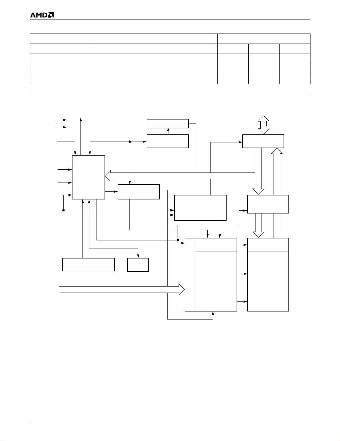
PRODUCT SELECTOR GUIDE
Family Part Number Am29LV033C
Speed Option Full Voltage Range: V
Max Access Time (ns) 70 90 120
CE# Access (ns) 70 90 120
OE# Access (ns) 30 40 50
= 2.7–3.6 V -70 -90 -120
CC
Note: See “AC Characteristics” for full specifications.
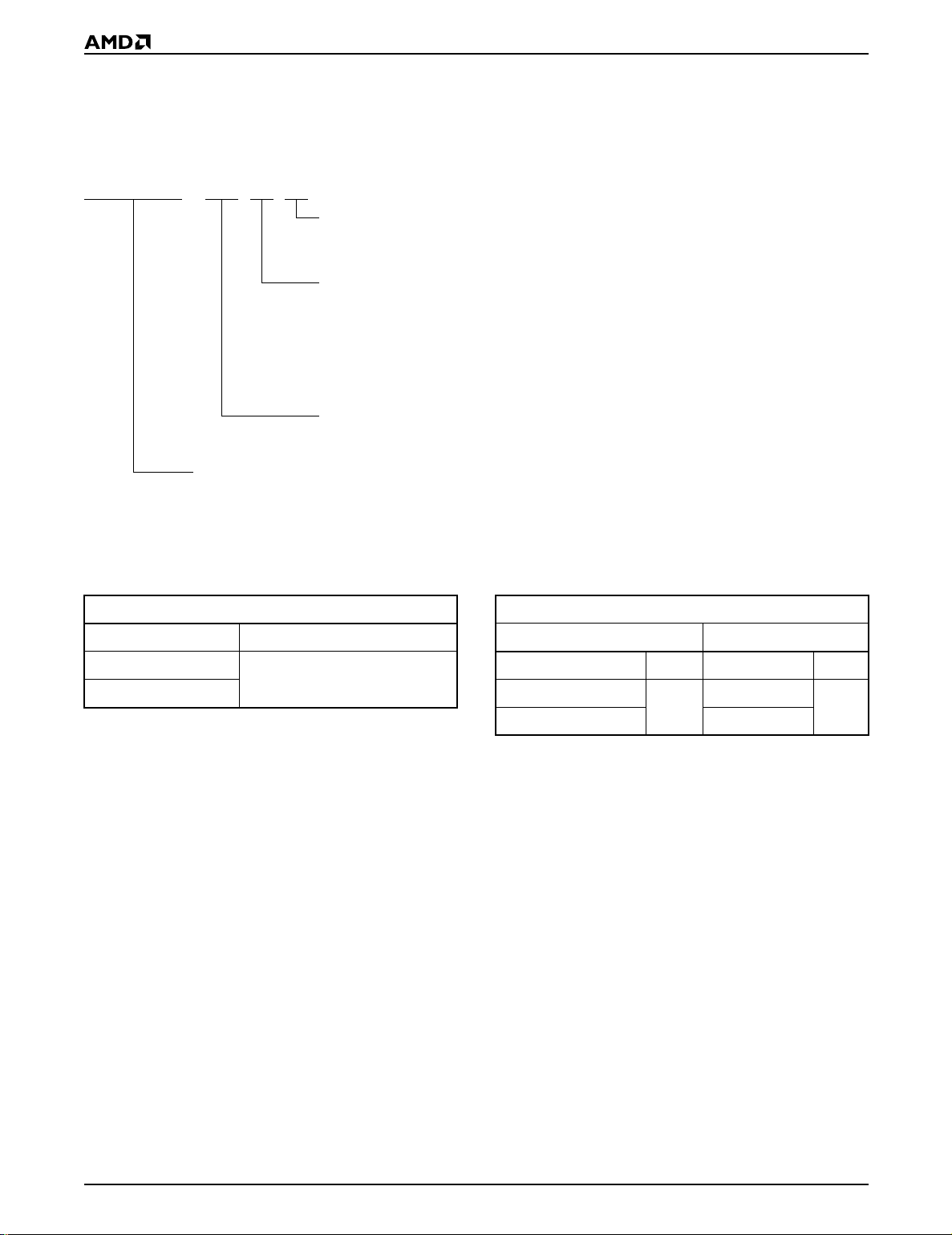
BLOCK DIAGRAM
DQ0
–
DQ7
Input/Output
Buffers
Data
Latch
V
CC
V
SS
RESET#
WE#
ACC
CE#
OE#
RY/BY#
State
Control
Command
Register
PGM Voltage
Generator
Sector Switches
Erase Voltage
Generator
Chip Enable
Output Enable
Logic
STB
A0–A21
VCC Detector
Timer
STB
Address Latch
Y-Decoder
X-Decoder
Y-Gating
Cell Matrix
4 Am29LV033C
Page 6
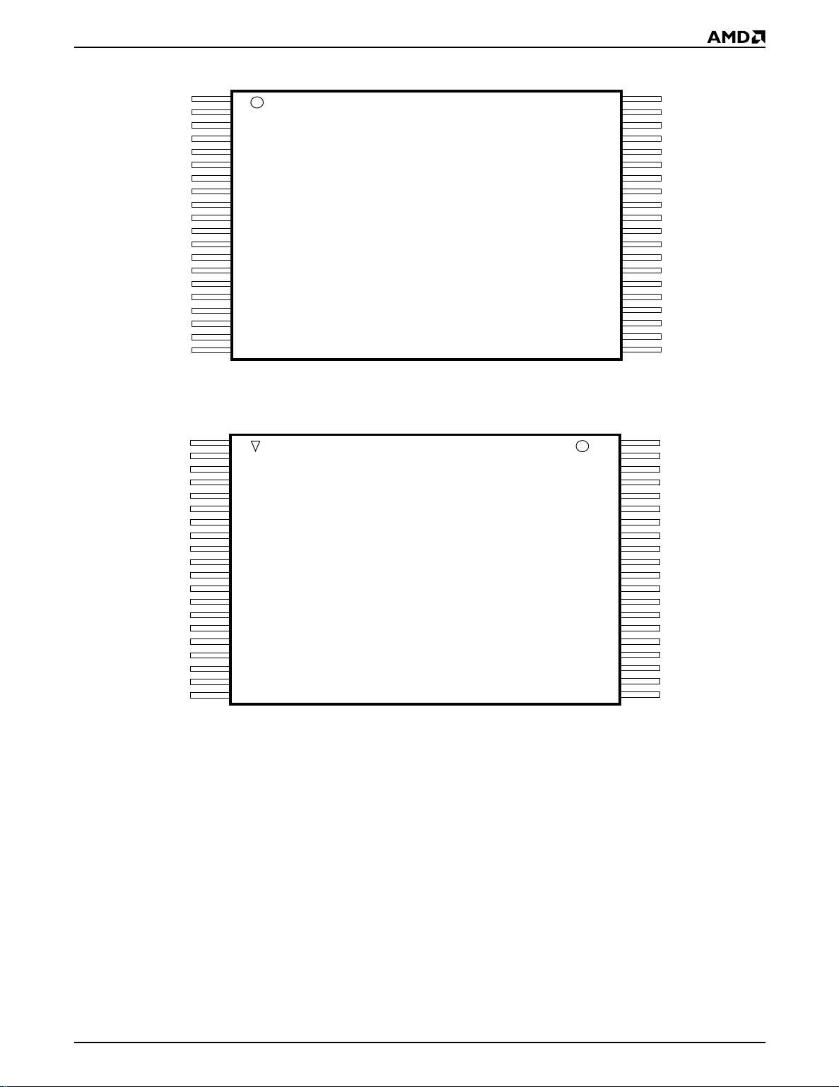
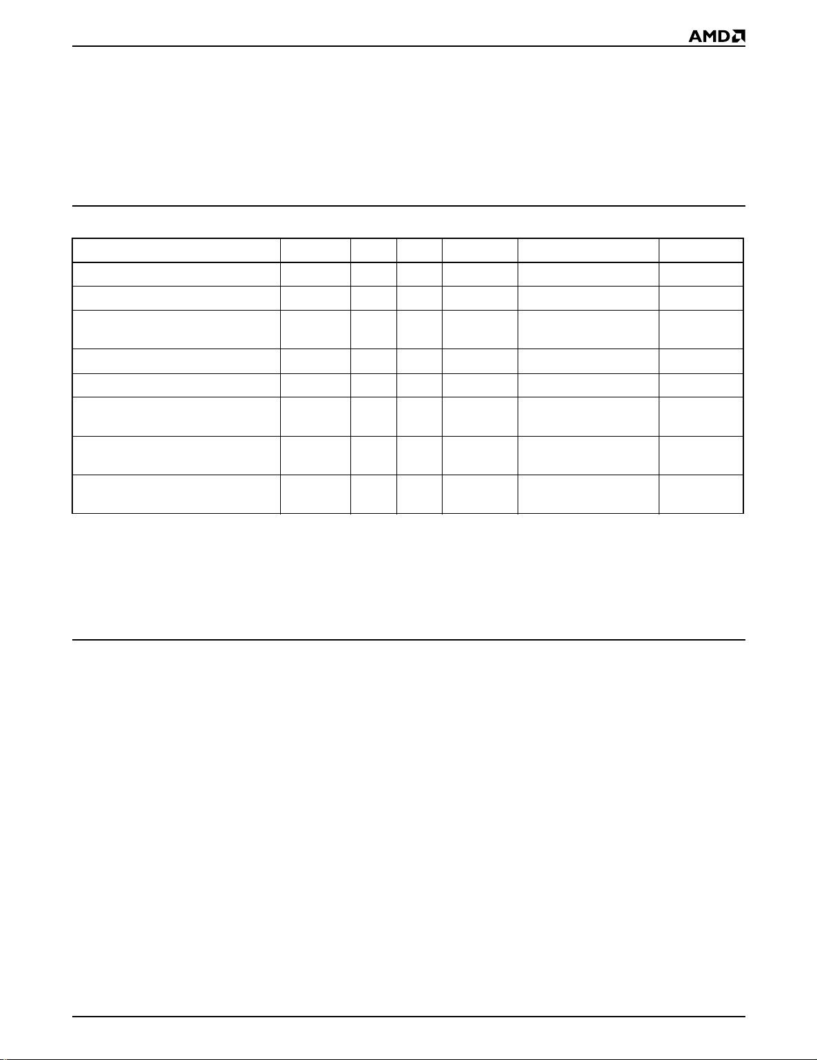
CONNECTION DIAGRAMS
A16
A15
A14
A13
A12
A11
A9
A8
WE#
RESET#
ACC
RY/BY#
A18
A7
A6
A5
A4
A3
A2
A1
A17
V
SS
A20
A19
A10
DQ7
DQ6
DQ5
DQ4
V
CC
V
CC
A21
DQ3
DQ2
DQ1
DQ0
OE#
V
SS
CE#
A0
1
2
3
4
5
6
7
8
9
10
11
12
13
14
15
16
17
18
19
20
1
2
3
4
5
6
7
8
9
10
11
12
13
14
15
16
17
18
19
20
40-Pin Standard TSOP
40-Pin Reverse TSOP
40
39
38
37
36
35
34
33
32
31
30
29
28
27
26
25
24
23
22
21
40
39
38
37
36
35
34
33
32
31
30
29
28
27
26
25
24
23
22
21
A17
V
SS
A20
A19
A10
DQ7
DQ6
DQ5
DQ4
V
CC
V
CC
A21
DQ3
DQ2
DQ1
DQ0
OE#
V
SS
CE#
A0
A16
A15
A14
A13
A12
A11
A9
A8
WE#
RESET#
ACC
RY/BY#
A18
A7
A6
A5
A4
A3
A2
A1
Am29LV033C 5
Page 7
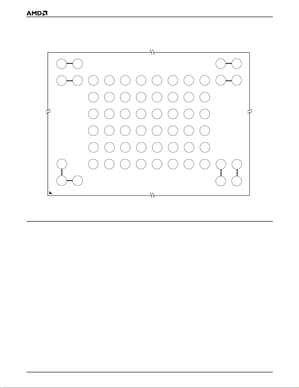
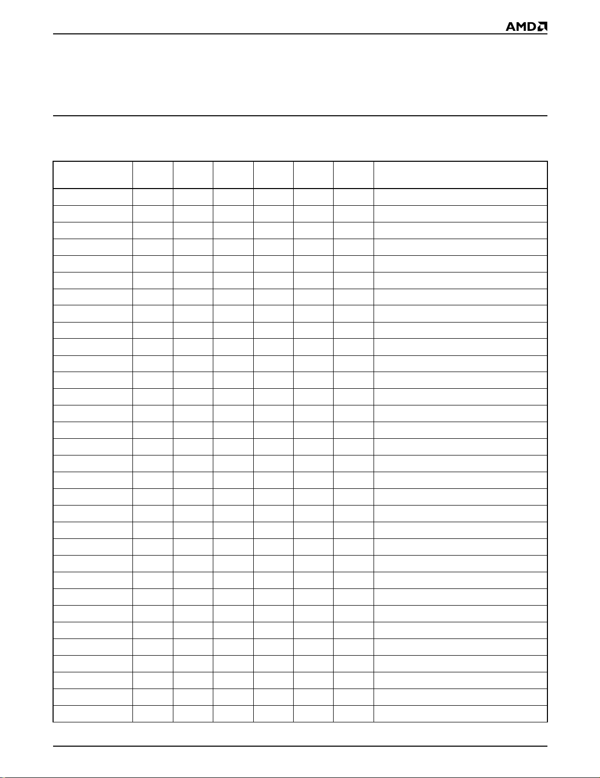
CONNECTION DIAGRAMS
63-Ball FBGA (Top View, Balls Down)
A8 B8
NC* NC*
A7 B7
NC*NC*
A2
NC*
A1 B1
NC* NC*
C7 D7 E7
A14 A13 A15 A16 A17 NC A20 V
C6 D6 E6 F6 G6 H6 J6 K6
A9 A8 A11 A12 A19 A10 DQ6 DQ7
C5 D5 E5 F5 G5 H5 J5 K5
WE# RESET# NC NC DQ5 NC V
C4 D4 E4
RY/BY# ACC NC NC DQ2 DQ3 V
C3 D3
A7 A18 A6 A5 DQ0 NC NC DQ1
C2 D2
A3 A4 A2 A1 A0 CE# OE# V
* Balls are shorted together via the substrate but not connected to the die.
E3
E2
F7 G7 H7 J7 K7
CC
F4 G4 H4 J4 K4
CC
F3
F2
G3
G2
H3
H2
J3
J2
SS
DQ4
A21
K3
K2
SS
L8 M8
NC* NC*
L7 M7
NC* NC*
L2
NC* NC*
L1
NC* NC*
M2
M1
Special Handling Instructions for FBGA
Packages
Special handling is required for Flash Memory
products in FBGA packages.
Flash memory devices in FBGA packages may be
damaged if exposed to ultrasonic cleaning methods.
The package and/or data integrity may be compromised
if the package body is exposed to temperatures above
150°C for prolonged periods of time.
6 Am29LV033C
Page 8
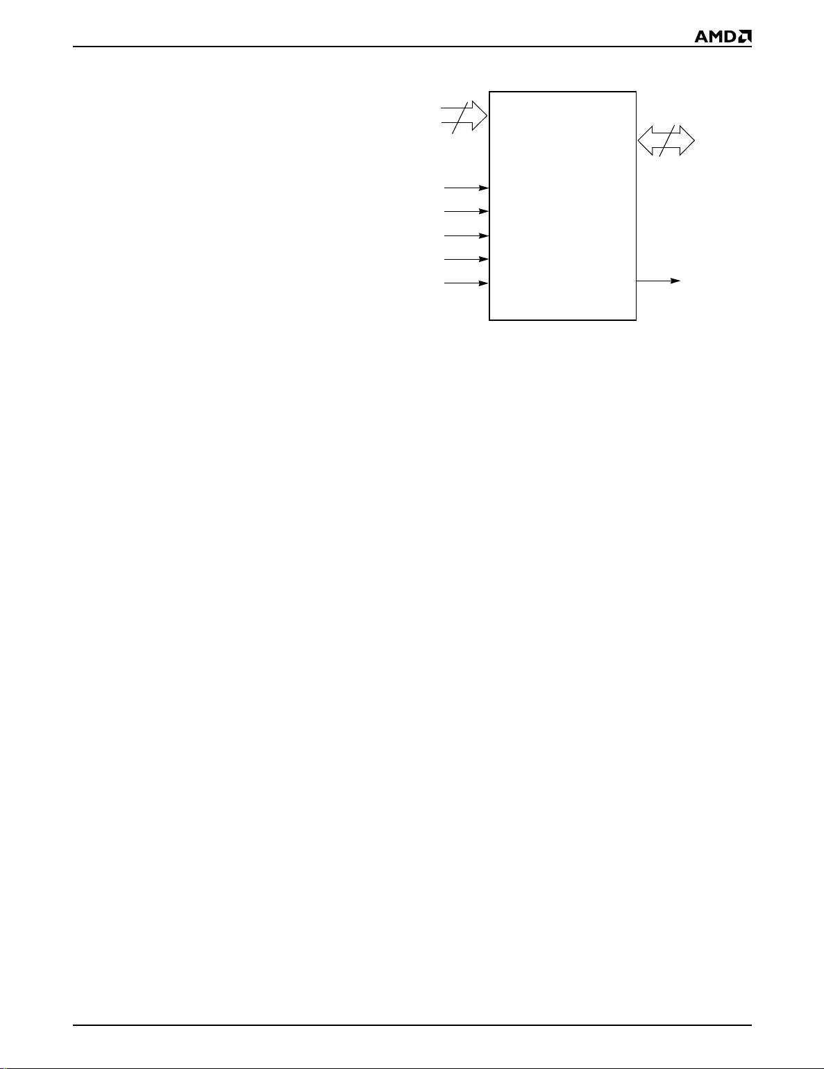
PIN CONFIGURATION
A0–A21 = 22 addresses
DQ0–DQ7 = 8 data inputs/outputs
CE# = Chip enable
OE# = Output enable
LOGIC SYMBOL
22
A0–A21
8
DQ0–DQ7
WE# = Write enable
RESET# = Hardware reset pin, active low
RY/BY# = Ready/Busy output
ACC = Hardware Acc e l eration Pin
= 3.0 volt-only single power supply
V
CC
(see Product Selector Guide for speed
options and voltage supply t olerances)
V
SS
= Device ground
NC = Pin not connected internally
CE#
OE#
WE#
RESET#
ACC
RY/BY#
Am29LV033C 7
Page 9
ORDERING INFORMATION
Standard Pr od ucts
AMD standard products are available in several packages and operating ranges. The order number (Valid Combination) is formed by a combination of the elements below.
Am29LV033C -70 E C
TEMPERATURE RANGE
I = Industrial (–40
E = Extended (–55
PACKAGE TYPE
E = 40-Pin Thin Small Outline Package (TSOP)
Standard Pinout (TS 040)
F = 40-Pin Thin Small Outline Package (TSOP)
Reverse Pinout (TSR040)
WD = 63-ball Fine-Pitch Ball Grid Array (FBGA)
0.80 mm pitch, 8 x 14 mm package (FBD063)
SPEED OPTION
See Product Selector Guide and Valid Combinations
DEVICE NUMBER/DESCRIPTION
Am29LV033C
32 Megabit (4 M x 8-Bit) CMOS Flash Memory
3.0 Volt-only Read, Program and Erase
°C to +85°C)
°C to +125°C)
Valid Combinations for TSOP Packages
AM29LV033C-70 EI, FI
AM29LV033C-90
AM29LV033C-120
Valid Combinations
Valid Combinations list configurations planned to be supported in volume f or this device. Consult the local AMD sales
office to confirm av ailability of specific valid combinations and
to check on newly released combinations.
EI, EE,
FI, FE
Valid Combinations for FBGA Packages
Order Number Package Marking
AM29LV033C-70 WDI L033C70V I
AM29LV033C-90
AM29LV033C-120 L033C12V
WDI,
WDE
L033C90V
I, E
8 Am29LV033C
Page 10
DEVICE BUS OPERATIONS
This section describes the requirements and use of
the device bus operations, which are initiated through
the internal command register. The command register
itself does not occupy any addressa ble memor y loc ation. The register is composed of l atches that store the
commands, along with the a ddress an d data inform ation needed to execute the command. The contents of
Table 1. Am29LV033C Device Bus Operations
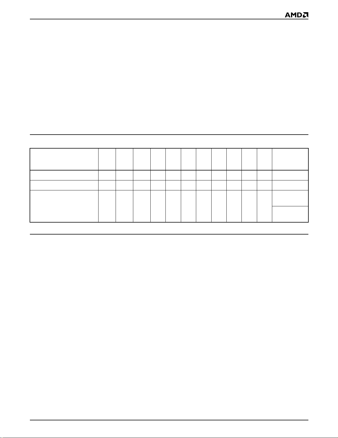
Operation CE# OE# WE# RESET# Addresses DQ0–DQ7
the register ser ve as inputs to th e intern al state machine. The state machine outputs dictate the function
of the device. Table 1 lists the device bus operations,
the inputs and control levels they require, and the resulting output. The following subsections describe
each of these operations in further detail.
Read L L H H A
Write (Note 1) L H L H A
±
V
Standby
Output Disable L H H H X High-Z
Reset X X X L X High-Z
Sector/Sector Block Protect
(Note 2)
Sector/Sector Block Unprotect
(Note 2)
Te mp orary Sector/Sector Block
Unprotect
CC
0.3 V
LHLV
LHLV
XXXV
XX
V
CC
0.3 V
ID
ID
ID
±
Sector Addresses,
A6 = L, A1 = H, A0 = L
Sector Addresses
A6 = H, A1 = H, A0 = L
IN
IN
X High-Z
A
IN
D
OUT
D
IN
, D
D
IN
OUT
, D
D
IN
OUT
D
IN
Legend:
L = Logic Low = V
, H = Logic High = VIH, VID = 12.0 ± 0.5 V, X = Don’t Care, AIN = Address In, D
IL
= Data In, D
IN
= Data Out
OUT
Notes:
1. When the ACC pin is at V
, the device enters the accelerated program mode. See “Accelerated Program Operations” for
HH
more information.
2. The sector protect and sector unprotect functions may also be implemented vi a progr amming equi pment. See the “Sect or/Sector
Block Protection and Unprote ction” secti on.
Requirements for Reading Array Data
To read array data from the outputs, the system must
drive the CE# and OE# pins to V
control and selects the device. OE# is the output control and gates array data to the output pins. WE#
should remain at V
.
IH
The internal state machine is set for reading arr ay data
upon device power-up, or after a hardware reset. This
ensures that no spurious alteration of the memory
content occurs during the power transition. No command is necessary in this mode to obtain array data.
Standard microprocessor read cycles that assert valid
addresses on the device address inputs produce valid
data on the device data outputs. The device remains
enabled for read access until the command register
contents are altered.
See “Reading Array Data” for more information. Refer
to the AC Read Operations table for timing specifica-
. CE# is the power
IL
Am29LV033C 9
tions and to Figure 13 for the timing diagram. I
CC1
in
the DC Characteristics table represents the active current specification for reading array data.
Writing Commands/Command Sequences
To wr ite a command or command sequence (which includes programming data to the device and erasing
sectors of memory), the system must drive WE# and
CE# to V
The device f eatures an Unlock Bypass mode to facili-
tate faster programming. Once the device enters the
Unlock Bypass mode, only two write cycles are required to program a byte, instead of four. The “Byte
Program Command Sequence” section has details on
programming data to the device using both standard
and Unlock Bypass command sequences.
An erase operation can erase one sect or, multiple sectors, or the entire de vi ce. Table 2 indicates the address
, and OE# to VIH.
IL
Page 11

space that each sector occupies. A “sector address ”
consists of the address bits required to uniquely select
a sector. The “Comm and D efinitio ns” s ection has de tails on erasing a sector or the entire chip , or suspending/resuming the erase operation.
After the system wr ites the autosele ct command s equence, the device enters the autoselect mode. The
system can then read autoselect codes from the internal register (which is separate from the memory array)
on DQ7–DQ0. Standard read cycle timings apply in
this mode. Refer to the Autoselect Mode and Autoselect Command Sequence sections for more information.
in the DC Characteristics table represents the ac-
I
CC2
tive current specification for the write mode. The “AC
Characteristics” section contains timing specification
tables and timing diagrams for write operations.
Accelerated Program Operation
The device offers accelerated program operations
through the ACC function. This is one of two functions
provided by the ACC pin. This function is prim arily intended to allow faster manufacturing throughput at the
factory.
If the system a sser t s V
on this pin, the device auto-
HH
matically enters the aforementioned Unlock Bypass
mode, temporarily unprotects any protected s ectors,
and uses the higher voltage on the pin to reduce the
time required for program operations. The system
would use a two-cyc le program comm and seq uence
as required by the Unlock Bypass mode. Removing
from the ACC pin returns the device to normal op-
V
HH
eration. Note that the ACC pin must not be at V
HH
for
operations other than accelerated programming, or
device damage may result.
Program and Erase Operation Status
During an erase or program operation, the system
may check the status of the operation by reading the
status bits on DQ7–DQ0. Standard read cycle timings
and I
read specifications apply. Refer to “Write Op-
CC
eration Status” for more information, and to “AC Characteristics” for timing diagrams .
Standby Mode
When the system is not reading or writing to the device, it can place the device in the standby mode. In
this mode, current consumption is greatly reduced,
and the outputs are placed in the high impedance
state, independent of the OE# input.
The device enters the CMOS standby mode when the
CE# and RESET# pin s are both held at V
(Note that this is a more restricted voltage range than
.) If CE# and RESET# are held at VIH, but not within
V
IH
± 0.3 V, the device will be in the standby mode , b ut
V
CC
± 0.3 V.
CC
the standby current will be greater. The device requires standard access time (t
) for read access
CE
when the device is in either of these standby modes,
before it is ready to read data.
The device also enters the standby mode when the
RESET# pin is driven low. Refer to the next section,
“RESET#: Hardware Reset Pin”.
If the device is deselected during erasure or programming, the device draws active current until the
operation is completed.
in the DC Characteristics table represents the
I
CC3
standby current specification.
Automatic Sleep Mode
The automatic sleep mod e minimizes Fla sh device
energy consumption. The device automatica lly
enables this mode when addresses remain stable for
+ 30 ns. The automatic sleep mode is
t
ACC
independent of the CE#, WE#, and OE# control
signals. Standard address access timings provide new
data when addresses are changed. While in sleep
mode, output data is latched and always available to
the system. I
in the DC Characteristics table
CC4
represents the automatic sleep mode current
specification.
RESET#: Hardware Reset Pin
The RESET# pin provides a hardware method of resetting the device to reading array data. When the RESET# pin is driven low for at least a period of t
device immediately terminates any operation in
progress, tristates all output pins, and ignores all
read/write comm ands for the duration of the RESET#
pulse. The device also resets the internal state machine to reading array data. The operation that was interrupted should be reinitiated once the device is
ready to acce pt another command sequenc e, to ensure data integrity.
Current is reduced for the duration of the RESET#
pulse. When RESET# is held at V
draws CMOS standby cu rrent ( I
but not within VSS±0.3 V, the standby current will
at V
IL
±0.3 V, the device
SS
). If RESET# is held
CC4
be greater.
The RESET# pin may be tied to the system reset cir-
cuitry. A system reset would thus also reset the Flash
memory, enabling the system to read the boot-up firmware from the Flash memory.
If RESET# is asserted during a program or erase operation, the RY/BY# pin rema ins a “0” (busy) until the
internal reset operation is complete, which requires a
time of t
(during Embedded Algorithms). The sys-
READ Y
tem can thus monitor RY/BY# to deter mine whethe r
the reset operation is complete. If RESET# is asserted
when a program or erase operation is not executing
(RY/BY# pin is “1”), the reset operation is completed
RP
, the
10 Am29LV033C
Page 12
within a time of t
rithms). The system can rea d data t
SET# pin returns to V
Refer to the AC Characteristics tables for RESET# pa-
(not during Em bedded Algo-
READY
.
IH
RH
after the R E-
Output Disable Mode
When the OE# input is at VIH, output from the devi ce is
disabled. The output pins are placed in the high impedance state.
rameters and to Figure 14 for the timing diagram.
Table 2. Am29LV033C Sector Address Table
Address Range
Sector A21 A20 A19 A18 A17 A16
SA0 000000 000000–00FFFF
SA1 000001 010000–01FFFF
SA2 000010 020000–02FFFF
SA3 000011 030000–03FFFF
SA4 000100 040000–04FFFF
SA5 000101 050000–05FFFF
SA6 000110 060000–06FFFF
SA7 000111 070000–07FFFF
SA8 001000 080000–08FFFF
SA9 001001 090000–09FFFF
SA10 001010 0A0000–0AFFFF
SA11 001011 0B0000–0BFFFF
SA12 001100 0C0000–0CFFFF
SA13 001101 0D0000–0DFFFF
SA14 001110 0E0000–0EFFFF
SA15 001111 0F0000–0FFFFF
SA16 010000 100000–10FFFF
SA17 010001 110000–11FFFF
SA18 010010 120000–12FFFF
SA19 010011 130000–13FFFF
SA20 010100 140000–14FFFF
SA21 010101 150000–15FFFF
SA22 010110 160000–16FFFF
SA23 010111 170000–17FFFF
SA24 011000 180000–18FFFF
SA25 011001 190000–19FFFF
SA26 011010 1A0000–1AFFFF
SA27 011011 1B0000–1BFFFF
SA28 011100 1C0000–1CFFFF
SA29 011101 1D0000–1DFFFF
SA30 011110 1E0000–1EFFFF
SA31 011111 1F0000–1FFFFF
(in hexadecimal)
Am29LV033C 11
Page 13
Table 2. Am29LV033C Sector Address Table (Continued)
Address Range
Sector A21 A20 A19 A18 A17 A16
SA32 100000 200000–20FFFF
SA33 100001 210000–21FFFF
SA34 100010 220000–22FFFF
SA35 100011 230000–23FFFF
SA36 100100 240000–24FFFF
SA37 100101 250000–25FFFF
SA38 100110 260000–26FFFF
SA39 100111 270000–27FFFF
SA40 101000 280000–28FFFF
SA41 101001 290000–29FFFF
SA42 101010 2A0000–2AFFFF
SA43 101011 2B0000–2BFFFF
SA44 101100 2C0000–2CFFFF
SA45 101101 2D0000–2DFFFF
SA46 101110 2E0000–2EFFFF
SA47 101111 2F0000–2FFFFF
SA48 110000 300000–30FFFF
SA49 110001 310000–31FFFF
SA50 110010 320000–32FFFF
SA51 110011 330000–33FFFF
SA52 110100 340000–34FFFF
SA53 110101 350000–35FFFF
SA54 110110 360000–36FFFF
SA55 110111 370000–37FFFF
SA56 111000 380000–38FFFF
SA57 111001 390000–39FFFF
SA58 111010 3A0000–3AFFFF
SA59 111011 3B0000–3BFFFF
SA60 111100 3C0000–3CFFFF
SA61 111101 3D0000–3DFFFF
SA62 111110 3E0000–3EFFFF
SA63 111111 3F0000–3FFFFF
(in hexadecimal)
Note: All sectors are 64 Kbytes in size.
12 Am29LV033C
Page 14
Autoselect Mode
The autoselect mode provides manufacturer and device identification, a nd sector pr otection verificatio n,
through identifier codes output on DQ7–DQ0. This
mode is prima rily intende d for programming equipment to automatically match a device to be programmed with its corresponding programming
algorithm. However, the autoselect codes can also be
accessed in-system through the command register .
When using programming equipment, the autoselect
mode requires V
A9. Address pins A6, A1, and A0 must be as shown in
Table 3. In addition, when verifying sector protection,
the sector address must appear on the appropriate
highest order address bits (see Table ). Table 3 shows
Description CE# OE# WE#
(11.5 V to 12.5 V) on address pin
ID
Table 3. Am29LV033C Autoselect Codes (High Voltage Method)
A21
to
A16
the remaining address bits that are don’t care. When
all necessar y bits have been set as required , the programming equipment may then read the corresponding identifier code on DQ7-DQ0.
To access the autoselect codes in-system, the host
system can issue the autoselect command via the
command re gister, as shown in Table 9. This meth od
does not require V
. See “Writing specific addr ess
ID
and data commands or s equences into the co mmand
register initiates device operations. Table 9 defines the
valid register command sequences. Writing incorrect
address and data values or writing them in the improper sequence resets the device to reading array
data.” for details on using the autoselect mode.
A15
to
A10 A9
A8
to
A7 A6
A5
to
A2 A1 A0
DQ7
to
DQ0
Manufacturer ID: AMD L L H X X V
Device ID: Am29LV033C L L H X X V
Sector Protection Verification L L H SA X V
L = Logic Low = VIL, H = Logic High = VIH, SA = Sector Address, X = Don’t care.
Sector/Sector Block Protection and Unprotection
(Note: For the following discussion, the term “sector”
applies to both sectors and sector blocks. A sector
block consists of two or more a djace nt secto rs that a re
protected or unprotected at the same time (see Table 4).
The hardware sector protection feature disables both
program and erase operations in any sect or. The hardware sector unprotection feature re-enables both program and erase operations in previously protected
sectors. Sector protection/unprotection can be implemented via two methods.
The primary method requires V
only, and can be implemented either in-system or via
programming equipment. Figure 2 shows the algorithms and Figure 22 shows the timing diagram. This
method uses standard microprocessor bus cycle tim-
on the RESET# pin
ID
ing. For sector unprotect, all unprotected sectors must
first be protected prior to the first sector unprotect
write cycle.
The alternate method intended only for programming
equipment requires V
This method is compatible with programmer routines
written for earlier 3.0 volt-only AMD flash devices.
Publication number 22269 contains further details;
contact an AMD representative to request a copy.
The device is shipped with all sec tors unprotected.
AMD offers the option of programmi ng and pro tecting
sectors at its factory prior to shipping the device
through AMD’s ExpressFlash™ Service. Contact an
AMD representative for details.
It is possible to determine whether a sector is protected or unprotected. See “Autoselect Mode” for details.
XLXLL 01h
ID
XLXLH A3h
ID
XLXHL
ID
01h
(protected)
00h
(unprotected)
on address pin A9 and OE#.
ID
Am29LV033C 13
Page 15
Table 4. Sector Block Addresses for
Protection/Unprotection
Sector/
Sector Block A21–A16
SA0
SA1-SA3
SA4-SA7
SA8-SA11
SA12-SA15
SA16-SA19
SA20-SA23
SA24-SA27
SA28-SA31
SA32-SA35
SA36-SA39
SA40-SA43
SA44-SA47
SA48-SA51
SA52-SA55
SA56-SA59
SA60-SA62
SA63
000000 64 Kbytes
000001,000010,
000011
000100, 000101,
000110, 000111
001000, 001001,
001010, 001011
001100, 001101,
001110, 001111
010000, 010001,
010010, 010011
010100, 010101,
010110, 010111
011000, 011001,
011010, 011011
011100, 011101,
011110, 011111
100000, 100001,
100010, 100011
100100, 100101,
100110, 100111
101000, 101001,
101010, 101011
101100, 101101,
101110, 101111
110000, 110001,
110010, 110011
110100, 110101,
110110, 110111
111000, 111001,
111010, 111011
111100, 111101,
111110
111111 64 Kbytes
Sector/
Sector Block Size
192 (3x64) Kbytes
256 (4x64) Kbytes
256 (4x64) Kbytes
256 (4x64) Kbytes
256 (4x64) Kbytes
256 (4x64) Kbytes
256 (4x64) Kbytes
256 (4x64) Kbytes
256 (4x64) Kbytes
256 (4x64) Kbytes
256 (4x64) Kbytes
256 (4x64) Kbytes
256 (4x64) Kbytes
256 (4x64) Kbytes
256 (4x64) Kbytes
192 (4x64) Kbytes
Temporary Sector/Sector Block Unprotect
(Note: For the following discussion, the term “sector”
applies to both sectors and sector blocks. A sector
block consists of two or more adjacent sectors that are
protected or unprotected at the same time (see Table
4).
This feature allows temporary unprotection of previ-
ously protected sectors to change data in-system. The
Sector Unprotect mode is activated by setting the RESET# pin to V
sectors can be programmed or erased b y selecting the
sector addresses. Once V
SET# pin, all the previously protected s ectors are
protected again. Figure 1 shows the algorithm, and
Figure 21 shows the timing diagrams, for this feature.
. During this mode, former ly prot ected
ID
is removed from the RE-
ID
START
RESET# = V
(Note 1)
ID
Perform Erase or
Program Operations
RESET# = V
IH
Temporary Sector
Unprotect Completed
(Note 2)
Notes:
1. All protected sectors unprotected.
2. All previously protected sectors are protected once
Figure 1. Temporary Sector Unprotect Operation
14 Am29LV033C
again.
Page 16

Temporary Sector
Unprotect Mode
No
START
PLSCNT = 1
RESET# = V
Wait 1 µs
First Write
Cycle = 60h?
START
Protect all sectors:
The indicated portion
of the sector protect
ID
algorithm must be
performed for all
unprotected sectors
prior to issuing the
first sector
unprotect address
PLSCNT = 1
RESET# = V
Wait 1 µs
First Write
Cycle = 60h?
ID
No
Temporary Sector
Unprotect Mode
Increment
PLSCNT
No
PLSCNT
= 25?
Yes
Device failed
Sector Protect
Algorithm
Yes
Set up sector
address
Sector Protect:
Write 60h to sector
address with
A6 = 0, A1 = 1,
A0 = 0
Wait 150 µs
Verify Sector
Protect: Write 40h
to sector address
with A6 = 0,
A1 = 1, A0 = 0
Read from
sector address
with A6 = 0,
A1 = 1, A0 = 0
No
Data = 01h?
Yes
Protect another
sector?
No
Remove V
from RESET#
Write reset
command
Sector Protect
complete
Yes
No
All sectors
protected?
Yes
Set up first sector
address
Sector Unprotect:
Write 60h to sector
address with
A6 = 1, A1 = 1,
A0 = 0
Reset
PLSCNT = 1
Increment
PLSCNT
No
Yes
ID
PLSCNT
= 1000?
Yes
Device failed
Sector Unprotect
Wait 15 ms
Verify Sector
Unprotect: Write
40h to sector
address with
A6 = 1, A1 = 1,
A0 = 0
Read from
sector address
with A6 = 1,
A1 = 1, A0 = 0
No
Data = 00h?
Last sector
verified?
Remove V
from RESET#
Yes
Yes
Set up
next sector
address
No
ID
Algorithm
Write reset
command
Figure 2. In-System Sector Protect/
Unprotect Algorithms
Am29LV033C 15
Sector Unprotect
complete
Page 17

Hardware Data Protection
The command sequence requirement of unlock cycles
for programming or erasing pr ovides data pro tection
against inadvertent writes (refer to Table 9 for command definitions). In addition, the following hardware
data protection measures prevent accidental erasure
or programming, which might otherwise be caused by
spurious system level signals during V
power-up
CC
and power-down transitions, or from system noise.
Low V
When V
cept any write cycles. This protects data during V
Write Inhibit
CC
is less than V
CC
, the device does not ac-
LKO
CC
power-up and power-down. The command register
and all internal program/erase circuits are disabled,
and the device resets. Subsequent writes are ignored
until V
is greater than V
CC
. The system must pro-
LKO
COMMON FLASH MEMORY INTERFACE (CFI)
The Common Flash Interface (CFI) specification outlines device and host system software interrogation
handshake, which allows specific vendor-specified
software algorithms to be used for entire families of
devices. Software support can then be device-independent, JEDEC ID-independent, and forward- and
backward-compatible for the specified flash device
families. Flash vendors can standardize their existing
interfaces for long-term compatibility.
This device enters the CFI Query mode when the system writes the CFI Query command, 98h, to address
55h, any time the device is ready to read array data.
The system can read CFI information at the addresses
vide the proper signals to the control pins to prevent
unintentional writes when V
is greater than V
CC
LKO
.
Write Pulse “Glitch” Protection
Noise pulses of less than 5 ns (typical) on OE#, CE#
or WE# do not initiate a write cycle.
Logical Inhibit
Write cycles are inhibited by holding any one of OE# =
, CE# = VIH or WE# = VIH. To initiate a write cycle,
V
IL
CE# and WE# must be a logical zero while OE# is a
logical one.
Power-Up Write Inhibit
If WE# = CE# = V
and OE# = VIH during power up,
IL
the device does not accept commands on the rising
edge of WE#. The intern al state machi ne is automatically reset to reading array data on power-up.
given in Tables 5–8. To terminate reading CFI data,
the system must write the reset command.
The system can also write the CFI quer y command
when the device is in the autoselect mode. The device
enters the CFI query mode, and the system can read
CFI data at the addresses given in Tables 5–8. The
system must write the reset command to return the
device to the autoselect mode.
For further information, please refer to the CFI Specification and CFI Publication 100, a vailable via the W orld
Wide Web at http://www.amd.com/products/nvd/overview/cfi.html. Altern atively, contact an AMD representative for copies of these documents.
Table 5. CFI Query Identification String
Addresses Data Description
10h
11h
12h
13h
14h
15h
16h
17h
18h
19h
1Ah
51h
52h
59h
02h
00h
40h
00h
00h
00h
00h
00h
Query Unique ASCII string “QRY”
Primary OEM Command Set
Address for Primary Extended Table
Alternate OEM Command Set (00h = none exists)
Address for Alternate OEM Extended Table (00h = none exists)
16 Am29LV033C
Page 18

Table 6. System Interface String
Addresses Data Description
Min. (write/erase)
V
1Bh 27h
1Ch 36h
CC
D7–D4: volt, D3–D0: 100 millivolt
Max. (write/erase)
V
CC
D7–D4: volt, D3–D0: 100 millivolt
1Dh 00h V
1Eh 00h V
1Fh 04h Typical timeout per single byte/word write 2
20h 00h Typical timeout for Min. size buffer write 2
21h 0Ah Typical timeout per individual block erase 2
22h 00h Typical timeout for full chip erase 2
23h 05h Max. timeout for byte/word write 2
24h 00h Max. timeout for buffer write 2
25h 04h Max. timeout per individual block erase 2
26h 00h Max. timeout for full chip erase 2
Min. voltage (00h = no VPP pin present)
PP
Max. voltage (00h = no VPP pin present)
PP
N
ms (00h = not supported)
N
times typical
N
times typical
N
times typical (00h = not supported)
N
µs
N
µs (00h = not supported)
N
ms
N
times typical
Table 7. Device Geometry Definition
Addresses Data Description
N
27h 16h Device Size = 2
28h
29h
2Ah
2Bh
00h
00h
00h
00h
Flash Device Interface description (refer to CFI publication 100)
Max. number of byte in multi-byte write = 2
(00h = not supported)
byte
N
2Ch 01h Number of Erase Block Regions within device
2Dh
2Eh
2Fh
30h
31h
32h
33h
34h
35h
36h
37h
38h
39h
3Ah
3Bh
3Ch
3Fh
00h
00h
01h
00h
00h
00h
00h
00h
00h
00h
00h
00h
00h
00h
00h
Erase Block Region 1 Information
(refer to the CFI specification or CFI publication 100)
Erase Block Region 2 Information
Erase Block Region 3 Information
Erase Block Region 4 Information
Am29LV033C 17
Page 19

Table 8. Primary Vendor-Specific Extended Query
Addresses Data Description
40h
41h
42h
43h 31h Major version number, ASCII
44h 30h Minor version number, ASCII
45h 01h
46h 02h
47h 01h
48h 04h Sector Temporary Unprotect: 04 = Supported
49h 04h
4Ah 20h Simultaneous Operation: 20 = Not Supported
4Bh 00h Burst Mode Type: 00 = Not Supported, 01 = Supported
4Ch 00h
50h
52h
49h
Query-unique ASCII string “PRI”
Address Sensitive Unlock
0 = Required, 1 = Not Required
Erase Suspend
0 = Not Supported, 1 = To Read Only, 2 = To Read & Write
Sector Protect
0 = Not Supported, X = Number of sectors in per group
Sector Protect/Unprotect scheme
01 = 29F040 mode, 02 = 29F016 mode,
03 = 29F400 mode, 04 = 29LV800A mode
Page Mode Type: 00 = Not Supported, 01 = 4 Word Page,
02 = 8 Word Page
18 Am29LV033C
Page 20

COMMAND DEFINITIONS
Writing specific address and data commands or sequences into the command register initiates device operations. Table 9 defines the valid register command
sequences. Writin g incorrect address and da ta val-
ues or writing them in the improper sequence resets
the device to reading array data.
All addresses are latched on the falling edge of WE#
or CE#, whichever happens later. All data is latched on
the rising edge of WE# or CE#, whichever happens
first. Refer to the appropr iate timing di agrams in the
“AC Characteristics” section.
Reading Array Data
The device is automatically set to reading array data
after device power-up. No commands are required to
retrieve data. The device is also ready to read array
data after completing an Embedded Program or Embedded Erase algorithm.
After the device accepts an Er ase Suspend command,
the device enters the Erase Suspend mod e. The system can read array data using the standard read timings, except that if it reads at an address within
erase-suspended sectors, the device outputs status
data. After completing a programming operation in the
Erase Suspend mode, the system may once again
read array data with the same exception. See “Erase
Suspend/Erase Resume Commands” for more information on this mode.
The reset command may be written between the sequence cycles in an autoselect command sequence.
Once in the autoselect mod e, the reset command
must
be written to retur n to read ing array data (also
applies to autoselect during Erase Suspend).
If DQ5 goes high during a program or erase operation,
writing the reset command returns the device to reading array data (also applies during Erase Suspend).
Autoselect Command Sequence
The autoselect command sequence allows the host
system to access the manufacturer and devices
codes, and determine whether or not a sector is protected. Table 9 shows the address and data requirements. This method is an alternative to that shown in
Table 3, which is intended for PROM programmers
and requires V
The autoselect command sequence is initiated by writing two unlock cycles, followed by the autoselect command. The device then enters the autoselect mode,
and the system may read at any address any number
of times, without initiating another command sequence. A read cycle at address XX00h retrieves the
manufacturer code. A read cycle at address XX01h returns the device code. A read cycle containing a sector
address (SA) and the address 02h returns 01h if that
sector is protected, or 00h if it is unprotected. Refer to
Table for valid sector addresses.
on address bit A9.
ID
must
The system
able the device for reading array data if DQ5 goes
high, or while in the au toselect mode. See the “R eset
Command” section, next.
See also “Requirements for Reading Array Data” in
the “Device Bus Operations” section for more information. The Read Operations table provides the read parameters, and Figure 13 shows the timing diagram.
issue the reset command to re-en-
Reset Command
Writing the reset command to the device resets the
device to reading array data. Address bits are don’t
care for this command.
The reset command may be written between the sequence cycles in an erase command sequence before
erasing begins. This resets the device to reading array
data. Once erasure begins, however, the device ignores reset commands until the operation is complete.
The reset command may be written between the sequence cycles in a program command sequence before programming begins. This resets the device to
reading array data (al so applies to p rogramming in
Erase Suspend mode). O nce programming beg ins,
however, the device ignores reset commands until the
operation is complete.
The system must write the reset command to exit the
autoselect mode and return to reading array data.
Byte Program Command Sequence
The device programs one byte of data for each program operation. The command sequence requires four
bus cycles, and is initiated by writing two unlock write
cycles, followed by the program set-up command. The
program address and data are written next, which in
turn initiate the Embedded Program algor ithm. The
not
system is
timings. The device automatically generates the program pulses and verifies the programmed cell margin.
Ta ble 9 shows the address an d data requ irements for
the byte program command sequence.
When the Em bedded Program a lgorit hm is c omple te,
the device then returns to reading array data and addresses are no longer latched. The system can determine the status of the program operation by using
DQ7, DQ6, or RY/BY#. See “Write Operation Status”
for information on these status bits.
Any commands written to th e device duri ng the Embedded Program Algorithm are ignored. Note that a
hardware re set i mmediately ter mi nates the programming operation. The Byte Program command se-
required to provide further controls or
Am29LV033C 19
Page 21

quence should be reinitiated once the device has reset
to reading array data, to ensure data integrity.
Programming is allowed in any sequence and across
sector boundaries. A bit cannot be programmed
from a “0” back to a “1”. Attempting to do so may
halt the operation and set DQ5 to “1,” or cause the
Data# Polling algorithm to indicate the operation was
successful. However, a succeeding read will show that
the data is still “0”. Only erase operations can convert
a “0” to a “1”.
Unlock Bypass Command Sequence
The unlock bypass feature allows the system to program bytes to the device faster than using the standard program command sequence. Th e unloc k bypass
command sequence is initiated by first writing two unlock cycles. This is followed by a third write cycle containing the unlock bypass command, 20h. The device
then enters the unlock bypass mode. A two-cycle unlock bypass program command sequence is all that is
required to program in this mode. The first cycle in this
sequence contains the unlock bypass program com mand, A0h; the second cycle contains the program
address and data. Additional data is programmed in
the same manner. This mode dispenses with the initial
two unlock cycles required in the standard program
command sequence, resu lting in faster total programming time. Table 9 shows the requirements for the
command sequence.
Embedded
algorithm
in progress
Increment Address
Program
START
Write Program
Command Sequence
Data Poll
from System
Verify Data?
No
Last Address?
Programming
Completed
No
Yes
Yes
During the unlock bypass mode, only the Unlock Bypass Program and Unlock Bypass R eset commands
are valid. To exit the unlock bypass mode, the system
must issue the two-cycle unlock bypass reset command sequence. The first cycle must contain the data
90h; the second cycle the data 00h. Addresses are
don’t cares for both cycles. The device then returns to
reading array data.
Accelerated Program Operations
The device offers accelerated program operations
through the ACC pin. When t he syste m asserts V
HH
on
the ACC pin, the device automatically enters the Unlock Bypass mode. The system may then write the
two-cycle Unlock Bypass program command sequence, eliminating two cycles from the command sequence. In addition, the de v ice uses the higher voltage
on the ACC pin to accelerate the op eration.
the ACC pin must not be at V
during read or erase
HH
operations, or device damage may result
Note that
. If ACC is to
be permanently set, it is recommended that it be tied
to minimize current consumption.
to V
CC
Figure 3 illustrates the algorithm for the program operation. See the Erase/Program Operations table in “AC
Characteristics” for parameters, and to Figure 15 for
timing diagrams.
Note: See Table 9 for program command sequence.
Figure 3. Program Operation
Chip Erase Command Sequence
Chip erase is a six bus cycle opera tion. The chip er ase
command sequence is initiated by writing two unlock
cycles, followed by a set-up command. Two additional
unlock write cycles are then followed by the chip erase
command, which in turn invokes the Embedded Erase
not
algorithm. The device does
preprogram prior to erase. The Embedded Erase algorithm automatically preprograms and verifies the entire
memory for an all zero data pattern prior to electrical
erase. The system is not required to provide any controls or timings during these operations. Table 9 shows
the address and data requireme nts for the chip erase
command sequence.
Any commands writte n to the chip du ring th e Embedded Erase algorithm are ignored. Note that a hard-
ware reset during the chip erase operation
immediately terminates the operation. The Chip Erase
command sequence should be reinitiated once the de-
require the system to
20 Am29LV033C
Page 22

vice has returned to reading array data, to ensure data
integrity.
The system can determine the status of the erase operation by using DQ7, DQ6, DQ2, or RY/BY#. See
“Write Operation St atus” for informati on on these status bits. When the Embedded Erase algorithm is complete, the device returns to reading array data and
addresses are no longer latched.
Figure 4 illustrates the algorithm for the erase operation. See the Erase/Program Operations tables in “AC
Characteristics” for parameters, and to Figure 17 for
timing diagrams.
Sector Erase Command Sequence
Sector erase is a six bus cycle operation. The sector
erase command sequence is initiated by writing two
unlock cycles, followed by a set-up command. Two additional unlock write cycles are then followed by the
address of the sector to be erased, and the sector
erase command. Table 9 shows the address and data
requirements for the sector erase command sequence.
not
The device does
the memory prior to erase. The Embedded Erase algorithm automatically programs and verifies the sector
for an all zero data pattern prior to electrical erase.
The system is not required to provide any controls or
timings during these operations.
After the command sequence is written, a sector erase
time-out of 50 µs begins. During the time-out period,
additional sector ad dresses and se ctor erase commands may be written. Loading the sector erase buffer
may be done in any sequence, and the number of sectors may be from one sector to all sectors. The time
between these additional cycles must be less than 50
µs, otherwise the last address and command might
not be accepted, and erasure may begin. It is recommended that processor interrupts be disabled during
this time to ensure all comm ands are accepted . The
interrupts can be re-enabled after the last Sector
Erase command is written. If the time between additional sector erase commands can be assumed to be
less than 50 µs, the system need not monitor DQ3.
Any command other than Sector Erase or Erase
Suspend during the time-out period resets the device to reading array data. The system must rewrite
the command sequence and any additional sector addresses and commands.
The system can mon itor DQ3 to deter mine if the s ector erase timer has timed out. (See the “DQ3: Sector
Erase Timer” sectio n.) The time- out begins fr om the
rising edge of the final WE# pulse in the command sequence.
Once the sector erase operation has begun, only the
Erase Suspend command is valid. All other com-
require the system to preprogram
mands are ignored. Note that a hardware reset dur-
ing the sector erase operation immediately terminates
the operation. The Sector Erase command sequence
should be reinitiated once the device has returned to
reading array data, to ensure data integrity.
When the Embedded Erase algorithm is complete, the
device returns to reading array data and addresses
are no longer latched. The system can determine the
status of the erase operation by using DQ7, DQ6,
DQ2, or RY/ BY#. (Refer to “Write Operation Sta tus” for
information on these status bits.)
Figure 4 illustrates the algorithm for the erase operation. Refer to the Erase/Program Op erations ta bles in
the “AC Characteristics” section for parameters , and to
Figure 17 for timing diagrams.
Erase Suspend/Erase Resume Commands
The Erase Suspend command allows t he syste m to interrupt a sector erase operation and then read data
from, or program data to, any sector not selected for
erasure. This command is valid only during the sector
erase operation, including the time-out period 50 µs
during the sector erase command sequence. The
Erase Suspend command is ignored if written during
the chip erase operation or Embedd ed Program algorithm. Writing the Erase Suspend command during the
Sector Erase time-out immediately terminates the
time-out period and suspends the er ase oper at ion. Addresses are “don’t-cares” when writing the Erase Suspend command.
When the Erase Suspend command is written during a
sector erase operation, the device requires a maximum of 20 µs to suspend the erase ope ration. However, when the Erase Suspend command is wr itten
during the sector erase time-out, the device immediately terminates the time-out period and suspends the
erase operation.
After the erase operation has been suspended, the
system can read array data from or program data to
any sector not selected for erasu re. (The de vice “er ase
suspends” all sectors selected for erasure.) Normal
read and write timings and command definitions apply.
Reading at any addre ss within e rase-suspen ded sectors produces status data on DQ7–DQ0. The system
can use DQ7, or DQ6 and DQ2 together, to determine
if a sector is actively erasing or is erase-s uspended.
See “Write Operation Status” for information on these
status bits.
After an erase-s uspende d program ope ration is complete, the system can once again read array data
within non-suspended sectors. The system can determine the status of the program operation using th e
DQ7 or DQ6 status bits, just as in the standard pro-
Am29LV033C 21
Page 23

gram operation. See “Write Operat ion Status” f or more
information.
The system may also write the autoselect command
sequence when the device is in the Erase Suspend
mode. The device allows reading autose lect codes
even at addresses within erasing sectors, since the
codes are not stored in the memory array. When the
device exits the autoselect mode, the device reverts to
the Erase Suspend m ode, and is ready for another
valid operation. See “Autoselect Command Sequence”
for more information.
The system must write the Erase Resume command
(address bits are “don’t care”) to exit the erase suspend mode and continue the sector erase operation.
Further writes of the Resume command are ignored.
Another Erase Suspend command can be written after
the device has resumed erasing.
START
Write Erase
Command Sequence
Data Poll
from System
No
Data = FFh?
Erasure Completed
Embedded
Erase
algorithm
in progress
Yes
Notes:
1. See Table 9 for erase command sequence.
2. See “DQ3: Sector Erase Timer” for more information.
Figure 4. Erase Operation
22 Am29LV033C
Page 24

Table 9. Am29LV033C Command Definitions
Command Sequence
(Note 1)
Read (Note 5) 1 RA RD
Reset (Note 6) 1 XXX F0
Manufacturer ID (Note 8) 4 XXX AA XXX 55 0XXXXX 90 0XXX00 01
Device ID (Note 8) 4 XXX AA XXX 55 0XXXXX 90 0XXX01 A3
Sector Protect Verify
(Note 7)
Autoselect
(Note 9)
Byte Program 4 XXX AA XXX 55 XXX A0 PA PD
Unlock Bypass 3 XXX AA XXX 55 XXX 20
Unlock Bypass Program
(Note 10)
Unlock Bypass Reset
(Note 11)
Chip Erase 6 XXX AA XXX 55 XXX 80 XXX AA XXX 55 XXX 10
Sector Erase 6 XXX AA XXX 55 XXX 80 XXX AA XXX 55 SA 30
Erase Suspend (Note 12) 1 XXX B0
Erase Resume (Note 13) 1 XXX 30
CFI Query (Note 14) 1 XXX 98
First Second Third Fourth Fifth Sixth
Addr Data Addr Data Addr Data Addr Data Addr Data Addr Data
Cycles
XXX
4
XXX XXX 01
2 XXX A0 PA PD
2 XXX 90 XXX 00
AA
XXX
55
Legend:
X = Don’t care
RA = Address of the memory location to be read.
RD = Data read from location RA during read operation.
PA = Address of the memory location to be programmed. Ad-
dresses are latched on the falling edge of the WE# or CE#
pulse.
Bus Cycles (Notes 2–4)
0XXXXX
or
2XXXXX
90
SA
X02
00
PD = Data to be programmed at location PA. Data is latched on
the rising edge of WE# or CE# pulse.
SA = Address of the sector to be erased or verified. Address bits
A21–A16 uniquely select any sector.
Notes:
1. See Table 1 for descriptions of bus operations.
2. All values are in he xade cimal.
3. E xcept when r eadin g arr ay or autoselect data, all bus cycles
are write operations.
4. Addr ess bit s ar e do n’t ca re for unlock and comma nd cycles,
except when PA or SA is required.
5. No unlock or command cycles require d when device is in read
mode.
6. T he Reset command is required to ret urn to the read mode
when the device is in the autose lect m ode o r if DQ5 go es high .
7. T he fourth cycle of the autoselect command seque nce is a
read cycle.
8. I n the thir d a nd fourth cycles of the command sequence , se t
A21 to 0.
9. I n the thir d cycl e of the command sequence, addr ess bit A21
must be set to 0 if verifying sectors 0–31, or to 1 if verifying
sectors 32–64. The data in the fourth cycle is 00h for an
unprotected sector/sector b l ock and 01h for a protected
sector/sector bloc k.
10. The Unlock Bypass command is requir ed prior to the Un loc k
Bypass Program command.
11. The Unlock Bypass Reset command is req uire d to return to
reading array d ata when the device is in the Unlock Bypass
mode.
12. The system may re ad and pr ogram functions in non-er asing
sectors, or enter t he a utosele ct mo de , whe n in the E r ase
Suspend mode. The Erase Suspe nd com mand is valid only
during a sector erase oper a tion.
13. The Erase Resume command is valid only during the Erase
Suspend mode.
14. Command is valid when device is ready to read arr ay data or
when device is in auto select mode .
Am29LV033C 23
Page 25

WRITE OPERATION STATUS
The device provides several bits to determine the status of a write op eration: DQ2 , DQ3, DQ5 , DQ6, DQ7,
and RY/BY#. Table 10 and the following subsections
describe the functions of thes e bits. DQ7, RY/BY#,
and DQ6 each offer a method for determining whether
a program or erase operation is complete or in
progress. These three bits are discussed first.
DQ7: Data# Polling
The Data# Polling bit, DQ7, indicates to the host system whether an Embedded Algorithm is in progress or
completed, or whether the devic e is in Er as e Suspend.
Data# Polling is valid after the rising edge of the final
WE# pulse in the program or erase command sequence.
During the Embedded Program algorithm, the device
outputs on DQ7 the complement of the datum programmed to DQ7. This DQ7 status also applies to programming during Erase Suspend. When the
Embedded Program algorithm is complete, the device
outputs the datum programmed to DQ7. The system
must provide the program address to read valid status
information on DQ7. If a program address falls within a
protected sector, Data# Polling on DQ7 is active for
approximately 1 µs, then the device returns to reading
array data.
Table 10 shows the outputs for Data# Polling on DQ7.
Figure 5 shows the Data# Polling algorithm.
START
Read DQ7–DQ0
Addr = VA
Yes
No
DQ7 = Data?
No
DQ5 = 1?
Yes
During the E mbedd ed Erase algor ithm, D ata# Polling
produces a “0” on DQ 7. When the Embed ded Erase
algorithm is complete, or if the device enters the Erase
Suspend mode, Data# Polling produces a “1” on DQ7.
This is analogous to the complement/true datum output described for the Embed ded Program algor ithm:
the erase function chan ges all the b its in a sector to
“1”; prior to this, the device outputs the “complement,”
or “0.” The system must provide an address within any
of the sectors selected for erasure to read valid status
information on DQ7.
After an era se comman d sequence is writte n, if all
sectors selected for erasing are protected, Data# Polling on DQ7 is active for appro ximately 100 µs, then the
device returns to reading array data. If not all selected
sectors are protected, the Embedded Erase algorithm
erases the unprotected sectors, and ignores the selected sectors that are protected.
When the system detects DQ 7 has chan ged from th e
complement to tru e data, it can read valid data at
DQ7–DQ0 on the
following
read cycles. This is because DQ7 may change asynchronously with
DQ0–DQ6 while Output Enable (OE#) is asserted low.
Figure 18, Data# Polling Timings (During
Embedded Algorithms), in the “AC Characteristics”
section illustrates this.
Read DQ7–DQ0
Addr = VA
DQ7 = Data?
No
FAIL
Notes:
1. VA = Valid address for programming. During a sector
erase operation, a valid address is an address within
any sector selected for erasure. During chip erase, a
valid address is any non-protected sector address.
2. DQ7 should be rechecked even if DQ5 = “1” because
DQ7 may change simultaneously with DQ5.
Yes
PASS
Figure 5. Data# Polling Algorithm
24 Am29LV033C
Page 26

RY/BY#: Ready/Busy#
The RY/BY# is a dedicated, open-drain output pin that
indicates whether an Embedded Algorithm is in
progress or complete. The RY/BY# status is valid after
the rising edge of the final WE# pulse in the command
sequence. Since RY/BY# is an open-drain output, several RY/BY# pins can be tied together in parallel with a
pull-up resistor to V
If the output is low (Busy), the device is actively erasing or programming. (This includes programming in
the Erase Suspend mode.) If the output is high
(Ready), the device is ready to read array data (including during the Erase Suspend mode), or is in the
standby mode.
Table 10 shows the outputs for R Y/BY#. Fig ures 14, 15
and 17 shows RY/BY# for reset, program, and erase
operations, respectively.
CC
.
DQ6: Toggle Bit I
Toggle Bit I on DQ6 indicates whether an Embedded
Program or Erase algorithm is in progress or complete, or whether the device has entered the Erase
Suspend mode. Toggle Bit I may be read at any address, and is valid after the rising edge of the final
WE# pulse in the command sequence (prior to the
program or erase operation), and during the sector
erase time-out.
During an Embedded Program or Erase algorithm operation, successive read cycles to any address cause
DQ6 to toggle (The system may use either OE# o r
CE# to control the read cycles). When the operation is
complete, DQ6 stops toggling.
After an era se comman d sequence is writte n, if all
sectors selected for erasing are pro tected, DQ6 to g-
gles for approximately 100 µs, then returns to reading
array data. If not all select ed sectors are prot ected, the
Embedded Erase algorithm erases the unprotected
sectors, and ignores the selected sectors that are protected.
The system can use D Q6 and DQ 2 together to dete rmine whether a sector is actively erasing or is
erase-suspended. When the device is actively erasing
(that is, the Embedded Er ase alg orithm is in pr og ress),
DQ6 toggles. When the device enters th e Erase Sus pend mode, DQ6 stops toggling. However, the system
must also use DQ2 to deter mine which sec tors are
erasing or erase-suspended. Alternatively, the system
can use DQ7 (see the subsection on DQ7: Data# Polling).
If a program address falls within a protected sector,
DQ6 toggles for approximately 1 µs after the program
command sequence is written, then returns to reading
array data.
DQ6 also toggles during the erase-suspend-program
mode, and stops toggling once the Embedded Program algorithm is complete.
Table 10 shows the outputs for Toggle Bit I on DQ6.
Figure 6 shows the toggle bit algorithm in flowchart
form, and the section “Reading Toggle Bits DQ6/DQ2”
explains the algorithm. Figure 19 in t he “A C Char ac teristics” section shows the toggle bit timing diagrams.
Figure 20 shows the differences between DQ2 and
DQ6 in graphical form. See also th e subsection o n
DQ2: Toggle Bit II.
DQ2: Toggle Bit II
The “Toggle Bit II” on DQ2, when used with DQ6, indicates whether a particular sector is actively erasing
(that is, the Embedded Erase algo rithm is in pro gress),
or whether that sector is erase-sus pended. Toggle Bit
II is valid after the rising edge of t he final WE# pulse in
the command sequence.
DQ2 toggles when the system reads at addresses
within those sectors that have been selected for erasure. (The system may use either OE# or CE# to control the read cycles.) But DQ2 cannot distinguish
whether the sector i s actively erasing or is erase-suspended. DQ6, by compar ison, indicates whe ther the
device is actively erasing, or is in Erase Suspend, but
cannot distingui sh which sectors ar e selected for erasure. Thus, both status bits are required for sector and
mode information. Refer to Table 10 to compare outputs for DQ2 and DQ6.
Figure 6 shows the toggle bit algorithm in flowchart
form, and the section “Reading Toggle Bits DQ6/DQ2”
explains the algorithm. See also the DQ6: Toggle Bit I
subsection. Figure 19 shows the toggle bit tim ing diagram. Figure 20 shows the differences between DQ2
and DQ6 in graphical form.
Reading Toggle Bits DQ6/DQ2
Refer to Figure 6 for the following discussion. Whenever the system initially begins reading toggle bit status, it must read DQ7–DQ0 at least twice in a row to
determine whether a toggle bit is toggling. Typically,
the system would note and sto re the value of the toggle bit after the first read. After the second read, the
system would compare the new value of the toggle bit
with the first. If the toggle bit is not toggling, the device
has completed the program or erase operation. The
system can read array data on DQ7–DQ0 on the following read cycle.
However, if after the initial two read cycles, the system
determines that the toggle bit is s till toggling, the system also should note whether the value of DQ5 is high
(see the section on DQ5). If it is, the system should
then determ ine again wheth er the toggle bi t is toggling, since the toggle bit may have stopped toggling
just as DQ5 went high. If the toggle bit is no longer
Am29LV033C 25
Page 27

toggling, the device has successfully completed the
program or erase operation. If it is still toggling , the device did not completed the operation successfully, and
the system must write the reset command to return to
reading array data.
START
The remaining scenario is that the system initially determines that the toggle bit is toggling and DQ5 has
not gone high. The system may continue to monitor
the toggle bit and DQ5 through successive read cycles, determining the status as described in the previous paragraph. Alternatively, it may choose to perform
other system tasks. In this case, the system must start
at the beginning of the algorithm when it returns to determine the status of the operation (top of Figure 6).
Table 10 shows the outputs for Toggle Bit I on DQ6.
Figure 6 shows the toggle bit algorithm. Figure 19 in
the “AC Characteristics” section shows the toggle bit
timing diagrams. Figure 20 shows the differences between DQ2 and DQ6 in graphical form. See also the
subsection on DQ2: Toggle Bit II.
DQ5: Exceeded Timing Limits
DQ5 indicates whether the program or erase time has
exceeded a specified internal pulse count limit. Under
these conditions DQ5 produ ces a “1.” This is a failure
condition that indicates the program or erase cycle
was not successfully completed.
The DQ5 failure condition may appear if the system
tries to program a “ 1” to a location that is previously
programmed to “0.” Only an erase operation can
change a “0” back to a “1.” Under this condition, the
device halts the operation, and when the operatio n
has exceeded the timing limits, DQ5 produces a “1.”
Under both these conditions, the system must issue
the reset command to re turn the device to readin g
array data.
No
Read DQ7–DQ0
Read DQ7–DQ0
Toggle Bit
= Toggle?
Yes
DQ5 = 1?
Yes
Read DQ7–DQ0
Twice
Toggle Bit
= Toggle?
Yes
Program/Erase
Operation Not
Complete, Write
Reset Command
(Note 1)
No
(Notes
1, 2)
No
Program/Erase
Operation Complete
DQ3: Sector Erase Timer
After writing a sector erase command sequence, the
Notes:
1. Read toggle bit twice to determine whether or not it is
system may read DQ3 to determine whether or not an
erase operation has begun. (The sector erase timer
2. Recheck toggle bit because it may stop toggling as DQ5
does not apply to the chip erase command.) If additional sectors are selected for erasure, the entire
time-out also applies after each additional sector
erase command. When the time-out is complete, DQ3
switches from “0” to “1.” If the time between additional
sector erase commands from th e system can b e assumed to be less than 50 µs, the system need not
monitor DQ3. See also the “Sector Erase Comm and
Sequence” section.
After the sector erase command sequence is written,
the system should read the status on DQ7 (Data# Polling) or DQ6 (Toggle Bit I) to ensure the device has accepted the command sequence, and then read DQ3. If
DQ3 is “1”, the internally controlled erase cycle has
begun; all further c ommands (other than Erase Suspend) are ignored until the erase ope ration is complete. If DQ3 is “0”, the device will accept additional
sector erase commands. To ensure the command has
been accepted, the system software should check the
status of DQ3 pr ior to and following each subseque nt
sector erase comma nd. If DQ3 is hig h on the secon d
status check, the last command might not have been
accepted. Table 10 shows the outputs for DQ3.
26 Am29LV033C
toggling. See text.
changes to “1”. See text.
Figure 6. Toggle Bit Algorithm
Page 28

Table 10. Write Operation Status
DQ7
Standard
Mode
Erase
Suspend
Mode
Operation
Embedded Program Algorithm DQ7# Toggle 0 N/A No toggle 0
Embedded Erase Algorithm 0 Toggle 0 1 Toggle 0
Reading within Erase
Suspended Sector
Reading within Non-Erase
Suspended Sector
Erase-Suspend-Program DQ7# Toggle 0 N/A N/A 0
(Note 2) DQ6
1 No toggle 0 N/A Toggle 1
Data Data Data Data Data 1
Notes:
1. DQ5 switches to ‘1’ when an Embedded Program or Embedded Erase operation has exceeded the maximum timing limits.
See “DQ5: Exceeded Timing Limits” for more information.
2. DQ7 and DQ2 require a valid address when reading status information. Refer to the appropriate subsection for further
details.
DQ5
(Note 1) DQ3
DQ2
(Note 2) RY/BY#
Am29LV033C 27
Page 29

ABSOLUTE MAXIMUM RATINGS
Storage Temperature
Plastic Packages . . . . . . . . . . . . . . . –65°C to +150°C
Ambient Temperature
with Power Applied. . . . . . . . . . . . . . –65°C to +125°C
Voltage with Respect to Ground
(Note 1) . . . . . . . . . . . . . . . . .–0.5 V to +4.0 V
V
CC
A9, OE#, and
RESET# (Note 2) . . . . . . . . . . . .–0.5 V to +12.5 V
All other pins (Note 1). . . . . . .–0.5 V to V
Output Short Circuit Current (Note 3) . . . . . . 200 mA
Notes:
1. Minimum DC voltage on input or I/O pins is –0.5 V.
During voltage transitions, input or I/O pins may
overshoot V
Figure 7. Maximum DC voltage on input or I/O pins is
V
+0.5 V. During voltage transitions, input or I/O pins
CC
may overshoot to V
Figure 8.
2. Minimum DC input voltage on pins A9, OE#, and RESET#
is –0.5 V. During voltage transitions , A9, OE#, and RESET#
may ov ershoot V
Figure 7. Maximum DC input voltage on pin A9 i s +12.5 V
which may overshoot to 14.0 V for periods up to 20 ns.
3. No more than one output may be shorted to ground at a
time. Duration of the s hort circuit should not be greater than
one second.
Stresses above those listed under “Absolute Maximum Ratings” may cause permanent damage to the device. This is a
stress rating only; functional operation of the device at these
or any other conditions above those indicated in the operational sections of this data sheet is not implied. Exposure of
the device to absolute maximum rating conditions for extended periods may affect device reliability.
to –2.0 V for periods of up to 20 ns. See
SS
+2.0 V for periods up to 20 ns. See
CC
to –2.0 V for periods of up to 20 ns. See
SS
CC
+0.5 V
OPERATING RANGES
Commercial (C) Devices
Ambient Temperature (T
Industrial (I) Devices
Ambient Temperature (T
Extended (E) Devices
Ambient Temperature (T
Supply Voltages
V
CC
for full voltage range. . . . . . . . . . . +2.7 V to 3.6 V
V
CC
Operating ranges define those limits between which the functionality of the device is guaranteed.
). . . . . . . . . . . .0°C to +70°C
A
). . . . . . . . . .–40°C to +85°C
A
). . . . . . . . .–55°C to +125°C
A
20 ns
V
CC
V
CC
+0.8 V
–0.5 V
V
SS
VSS–2.0 V
20 ns
20 ns
Figure 7. Maximum Negative
Overshoot Waveform
28 Am29LV033C
+2.0 V
+0.5 V
2.0 V
20 ns
20 ns
20 ns
Figure 8. Maximum Positive
Overshoot Waveform
Page 30

DC CHARACTERISTICS
CMOS Compatible
Parameter Description Test Conditions Min Typ Max Unit
V
= VSS to VCC,
I
I
I
LIT
I
LO
CC1
LI
Input Load Current (Note 1)
A9 Input Load Current VCC = V
Output Leakage Current
VCC Active Read Current
(Notes 2, 3)
IN
= VCC
V
CC
V
= VSS to VCC,
OUT
= V
V
CC
CE# = V
max
; A9 = 12.5 V 35 µA
CC max
CC max
5 MHz 10 16
, OE# = V
IL
IH
1 MHz 2 4
1.0 µA
±
1.0 µA
±
mA
V
V
V
I
I
I
I
I
V
V
CC2
CC3
CC4
CC5
ACC
V
V
V
OH1
OH2
LKO
IL
IH
HH
ID
OL
VCC Active Write Current
(Notes 2, 4, 6)
CE# = V
VCC Standby Current (Note 2) CE#, RESET#, ACC = VCC±
VCC Reset Current (Note 2)
Automatic Sleep Mode
(Notes 2, 5)
RESET# = V
ACC = V
V
IH
V
IL
ACC = V
ACC Accelerated Program
Current,
CE# = V
Word or Byte
= V
= V
OE# = V
IL,
CC
± 0.3 V;
CC
0.3 V,
±
SS
CC
, OE# = V
IL
SS
±
±
±
0.3 V
0.3 V
IH
0.3 V,
IH
15 30 mA
0.3 V 0.2 5 µA
0.2 5 µA
0.2 5 µA
ACC
pin
pin 15 30 mA
V
CC
510mA
Input Low Voltage –0.5 0.8 V
Input High Voltage 0.7 x V
CC
VCC + 0.3 V
Voltage for ACC Sector
Protect/Unprotect and Program
= 3.0 V ± 10% 8.5 9.5 V
V
CC
Acceleration
Voltage for Autoselect and
Temporary Sector Unprotect
Output Low Voltage IOL = 4.0 mA, VCC = V
Output High Voltage
Low VCC Lock-Out Voltage
(Note 6)
= 3.3 V 11.5 12.5 V
V
CC
0.45 V
CC min
I
= –2.0 mA, VCC = V
OH
IOH = –100 µA, VCC = V
0.85 V
CC min
V
CC min
CC
CC
–0.4
2.3 2.5 V
V
Notes:
1. On the ACC pin only, the maximum input load current when ACC = V
2. Maximum I
3. The I
4. I
CC
active while Embedded Erase or Embedded Program is in progress.
CC
specifications are tested with VCC = VCCmax.
CC
current listed is typically i s les s than 2 mA/MHz, with OE# at VIH. Typical specifications are for VCC = 3.0 V.
is ±5.0 µA.
IL
5. Automatic sleep mode enables the l ow p ower mode when addresses remai n stab le for t
200 nA.
6. Not 100% tested.
Am29LV033C 29
+ 30 ns. Typical sleep mode current is
ACC
Page 31

DC CHARACTERISTICS (Continued)
Zero Power Flash
25
20
15
10
Supply Current in mA
5
0
0 500 1000 1500 2000 2500 3000 3500 4000
Note: Addresses are switching at 1 MHz
Figure 9. I
Current vs. Time (Showing Active and Automatic Sleep Currents)
CC1
Time in ns
12
10
8
6
4
Supply Current in mA
2
0
12345
Note: T = 25 °C
3.6 V
2.7 V
Frequency in MHz
Figure 10. Typical I
vs. Frequency
CC1
30 Am29LV033C
Page 32

TEST CONDITIONS
3.3 V
Table 11. Test Specifications
Test Condition -70 -90, -120 Unit
Output Load 1 TTL gate
Output Load
Capacitance, C
(including jig capacitance)
Input Rise and Fall Times 5 ns
Input Pulse Levels 0.0–3.0 V
Input timing measurement
reference levels
L
Device
Under
Test
2.7 k
Ω
C
L
6.2 k
Ω
Note: Diodes are IN3064 or equivalent
Output timing measurement
Figure 11. Test Setup
reference levels
KEY TO SWITCHING WAVEFORMS
WAVEFORM INPUTS OUTPUTS
Steady
Changing from H to L
Changing from L to H
30 100 pF
1.5 V
1.5 V
3.0 V
0.0 V
Don’t Care, Any Change Permitted Changing, State Unknown
Does Not Apply Center Line is High Impedance State (High Z)
1.5 V 1.5 V
Figure 12. Input Waveforms and
Measurement Levels
OutputMeasurement LevelInput
Am29LV033C 31
Page 33

AC CHARACTERISTICS
Read Operations
Parameter
JEDEC Std Test Setup -70 -90 -120 Unit
t
AVAV
t
AVQV
t
ELQV
t
GLQV
t
EHQZ
t
GHQZ
Description
t
Read Cycle Time (Note 1) Min 70 90 120 ns
RC
t
Address to Output Delay
ACC
t
Chip Enable to Output Delay OE# = VILMax 70 90 120 ns
CE
t
Output Enable to Output Delay Max 30 40 50 ns
OE
t
Chip Enable to Output High Z (Note 1) Max 25 30 30 ns
DF
t
Output Enable to Output High Z (Note 1) Max 25 30 30 ns
DF
CE# = V
OE# = V
IL
Max 70 90 120 ns
IL
Speed Option
Read Min 0 ns
Output Enable
t
t
AXQX
OEH
Hold Time (Note 1)
Output Hold Time From Addresses, CE# or OE#,
t
OH
Whichever Occurs First (Note 1)
Toggle and
Data# Polling
Min 10 ns
Min 0 ns
Notes:
1. Not 100% tested.
2. See Figure 11 and Table 11 for test specifications.
t
RC
Addresses
CE#
OE#
WE#
Outputs
RESET#
RY/BY#
0 V
Addresses Stable
t
ACC
t
OE
t
OEH
t
CE
HIGH Z
Output Valid
Figure 13. Read Operations Timings
t
DF
t
OH
HIGH Z
32 Am29LV033C
Page 34

AC CHARACTERISTICS
Hardware Reset (RESET#)
Parameter
Description All Speed OptionsJEDEC Std Test Setup Unit
t
t
RESET# Pin Low (During Embedded Algorithms)
READY
to Read or Write (See Note)
RESET# Pin Low (NOT During Embedded
READY
Algorithms) to Read or Write (See Note)
RESET# Pulse Width Min 500 ns
t
RP
RESET# High Time Before Read (See Note) Min 50 ns
t
RH
RESET# Low to Standby Mode Min 20 µs
t
RPD
RY/BY# Recovery Time Min 0 ns
t
RB
Note: Not 100% tested.
RY/BY#
CE#, OE#
RESET#
t
RP
t
Ready
Max 20 µs
Max 500 ns
t
RH
RY/BY#
CE#, OE#
RESET#
Reset Timings NOT during Embedded Algorithms
Reset Timings during Embedded Algorithms
t
Ready
t
RP
Figure 14. RESET# Timings
t
RB
Am29LV033C 33
Page 35

AC CHARACTERISTICS
Erase/Program Operations
Parameter Speed Option
JEDEC Std Description -70 -90 -120 Unit
t
AVAV
t
AVWL
t
WLAX
t
DVWH
t
WHDX
t
GHWL
t
ELWL
t
WHEH
t
WLWH
t
WHWL
t
WHWH1
t
WHWH1
t
WHWH2
t
t
t
t
t
t
OES
t
GHWL
t
t
t
t
WPH
t
WHWH1
t
WHWH1
t
WHWH2
t
VCS
t
t
BUSY
Write Cycle Time (Note 1) Min 70 90 120 ns
WC
Address Setup Time Min 0 ns
AS
Address Hold Time Min 45 45 50 ns
AH
Data Setup Time Min 35 45 50 ns
DS
Data Hold Time Min 0 ns
DH
Output Enable Setup Time (Note 1) Min 0 ns
Read Recovery Time Before Write
(OE# High to WE# Low)
CE# Setup Time Min 0 ns
CS
CE# Hold Time Min 0 ns
CH
Write Pulse Width Min 30 45 50 ns
WP
Write Pulse Width High Min 30 ns
Programming Operation (Note 2) Typ 9 µs
Accelerated Programming Operation (Note 2) Typ 7 µs
Sector Erase Operation (Note 2) Typ 0.7 sec
VCC Setup Time (Note 1) Min 50 µs
Recovery Time from RY/BY# Min 0 ns
RB
Program/Erase Valid to RY/BY# Delay Min 90 ns
Notes:
1. Not 100% tested.
2. See the “Erase and Programming Performance” section f or more information.
Min 0 ns
34 Am29LV033C
Page 36

AC CHARACTERISTICS
Program Command Sequence (last two cycles)
t
WC
Addresses
XXXh
Read Status Data (last two cycles)
t
AS
PA PA
t
AH
PA
CE#
t
CH
OE#
t
WP
WE#
t
t
WPH
DH
Data
t
CS
t
DS
A0h
RY/BY#
t
VCS
V
CC
Note: PA = program address, PD = program data, D
Figure 15. Program Operation Timings
t
WHWH1
PD
t
BUSY
is the true data at the program address.
OUT
Status
D
OUT
t
RB
ACC
V
HH
V
or V
IL
IH V
t
VHH
Figure 16. Accelerated Program Timing Diagram
t
VHH
IL
or V
IH
Am29LV033C 35
Page 37

AC CHARACTERISTICS
Erase Command Sequence (last two cycles) Read Status Data
t
WC
Addresses
XXXh SA
CE#
t
t
CH
WP
OE#
WE#
t
CS
t
DS
t
DH
Data
55h
RY/BY#
t
VCS
V
CC
Note: SA = sector address (for Sector Erase), VA = Valid Address for reading status data (see “Write Operation Status”).
Figure 17. Ch ip/Sector Erase Operation Timings
t
AS
XXXh for chip erase
t
WPH
t
AH
30h
10 for Chip Erase
t
BUSY
t
WHWH2
VA
In
Progress
VA
Complete
t
RB
36 Am29LV033C
Page 38

AC CHARACTERISTICS
t
Addresses
CE#
t
CH
OE#
t
WE#
DQ7
OEH
t
ACC
t
RC
VA
t
CE
t
OE
t
DF
t
OH
Complement
VA VA
Complement
True
Valid Data
High Z
DQ0–DQ6
t
BUSY
Status Data
Status Data
True
Valid Data
RY/BY#
Note: VA = Valid address. Figure shows are first status cycle after command sequence, last status read cycle, and array data
read cycle.
Figure 18. Data# Polling Timings (During Embedded Algorithms)
RC
Addresses
CE#
OE#
WE#
DQ6/DQ2
RY/BY#
t
CH
t
BUSY
t
OEH
High Z
t
ACC
VA
t
CE
t
OE
t
DF
t
OH
(first read) (second read) (stops toggling)
VA VA
Valid Status
VA
Valid DataValid StatusValid Status
High Z
Note: VA = V alid address; not required for DQ6. Figure shows first two status cycle after command sequence, last status read cycle, and
array data read cycle.
Figure 19. Toggle Bit Timings (During Embedded Algorithms)
Enter
WE#
Embedded
Erasing
Erase
Erase
Suspend
Erase Suspend
Suspend Program
Read
Enter Erase
Erase
Suspend
Program
Erase Suspend
Read
Erase
Resume
Erase
Erase
Complete
DQ6
DQ2
Note: The system can use OE# or CE# to toggle DQ2/DQ6. DQ2 toggl es only when read at an address within an erase-suspended
sector.
Figure 20. DQ2 vs. DQ6
Am29LV033C 37
Page 39

AC CHARACTERISTICS
Temporary Sector/Sector Block Unprotect
Parameter
All Speed OptionsJEDEC Std Description Unit
t
VIDR
t
RSP
Note: Not 100% tested.
12 V
RESET#
0 or 3 V
CE#
WE#
RY/BY#
Figure 21. Temporary Sector/Sector Block Unprotect Timing Diagram
VID Rise and Fall Time (See Note) Min 500 ns
RESET# Setup Time for Temporary
Sector/Sector Block Unprotect
t
VIDR
Min 4 µs
t
VIDR
Program or Erase Command Sequence
t
RSP
38 Am29LV033C
Page 40

RESET#
V
ID
V
IH
SA, A6,
A1, A0
Valid* Valid* Valid*
Sector/Sector Block Protect or Unprotect Verify
Data
60h 60h 40h
Sector/Sector Block Protect: 150 µs,
Sector/Sector Block Unprotect: 15 ms
1 µs
CE#
WE#
OE#
Note: For sector protect, A6 = 0, A1 = 1, A0 = 0. For sector unprotect, A6 = 1, A1 = 1, A0 = 0.
Figure 22. Sector Pro tect/Unprotect
Timing Diagram
Status
Am29LV033C 39
Page 41

AC CHARACTERISTICS
Alternate CE# Controlled Erase/Program Operations
Parameter Speed Option
JEDEC Std Description -70 -90 -120 Unit
t
AVAV
t
AVEL
t
ELAX
t
DVEH
t
EHDX
t
GHEL
t
WLEL
t
EHWH
t
ELEH
t
EHEL
t
WHWH1
t
WHWH2
t
WC
t
AS
t
AH
t
DS
t
DH
t
OES
t
GHEL
t
WS
t
WH
t
CP
t
CPH
t
WHWH1
t
WHWH2
Write Cycle Time (Note 1) Min 70 90 120 ns
Address Setup Time Min 0 ns
Address Hold Time Min 45 45 50 ns
Data Setup Time Min 35 45 50 ns
Data Hold Time Min 0 ns
Output Enable Setup Time Min 0 ns
Read Recovery Time Before Write
(OE# High to WE# Low)
WE# Setup Time Min 0 ns
WE# Hold Time Min 0 ns
CE# Pulse Width Min 30 45 50 ns
CE# Pulse Width High Min 30 ns
Programming Operation (Note 2) Typ 9 µs
Sector Erase Operation (Note 2) Typ 0.7 sec
Notes:
1. Not 100% tested.
2. See the “Erase and Programming Performance” section for more information.
Min 0 ns
40 Am29LV033C
Page 42

AC CHARACTERISTICS
Addresses
WE#
OE#
CE#
Data
RESET#
XXX for program
XXX for erase
t
WC
t
WH
t
WS
t
RH
PA for program
SA for sector erase
XXX for chip erase
t
AS
t
GHEL
t
CP
t
CPH
t
DS
t
DH
A0 for program
55 for erase
t
AH
t
BUSY
PD for program
30 for sector erase
10 for chip erase
Data# Polling
t
WHWH1 or 2
PA
DQ7# D
OUT
RY/BY#
Notes:
1. PA = Program Address, PD = Program Data, D
= Data Out, DQ7# = complement of data written to device.
OUT
2. Figure indicates the last two bus cycles of the command seq uence .
Figure 23. Alternate CE# Controlled Write Operation Timings
Am29LV033C 41
Page 43

ERASE AND PROGRAMMING PERFORMANCE
Parameter Typ (Note 1) Max (Note 2) Unit Comments
Sector Erase Time 0.7 15 s
Chip Erase Time 45 s
Excludes 00h programming
prior to erasure (Note 4)
Byte Programming Time 9 300 µs
Accelerated Byte Program Time 7 210 µs
Excludes system level
overhead (Note 5)
Chip Programming Time (Note 3) 36 108 s
Notes:
1. Typical program and erase times assume the following conditions: 25
C, 3.0 V V
1,000,000 cycles. Additionally,
CC,
°
programming typicals assume checkerboard pattern.
2. Under worst case conditions of 90°C, V
= 2.7 V, 1,000,000 cycles.
CC
3. The typical chip programming time is considerably less than the maximum chi p prog r amming time list ed, si nce most b yt es
program fast er tha n the max im um prog r am t imes l isted.
4. In the pre-programming step of the Embedded Erase algorithm, all b yt es are prog r ammed to 00h before erasure.
5. System-level ove rhead is the ti me required to ex ecute the four - or two-b us-cycle sequence f or the prog ram command. See Table 9
for further information on command defi niti ons .
6. The device has a guaranteed minimum erase and program cycle endurance of 1,000,000 cycles.
LATCHUP CHARACTERISTICS
Description Min Max
Input voltage with respect to V
(including A9, OE#, and RESE T#)
Input voltage with respect to V
Current –100 mA +100 mA
V
CC
on all pins except I/O pins
SS
on all I/O pins –1.0 V VCC + 1.0 V
SS
–1.0 V 12.5 V
Includes all pins except VCC. Test conditions: VCC = 3.0 V, one pin at a time.
TSOP PIN CAPACITANCE
Parameter
Symbol Parameter Description Test Setup Typ Max Unit
C
IN
C
OUT
C
IN2
Input Capacitance VIN = 0 6 7.5 pF
Output Capacitance V
= 0 8.5 12 pF
OUT
Control Pin Capacitance VIN = 0 7.5 9 pF
Notes:
1. Sampled, not 100% tested.
2. Test conditions T
= 25°C, f = 1.0 MHz.
A
DATA RETENTION
Parameter Test Conditions Min Unit
Minimum Pattern Data Retention Time
150°C 10 Years
125°C 20 Years
42 Am29LV033C
Page 44

PHYSICAL DIMENSIONS*
TS 040—40-Pin Standard TSOP
* For reference only. BSC is an ANSI standard for Basic Space Centering.
Am29LV033C 43
Dwg rev AA; 10/99
Page 45

PHYSICAL DIMENSIONS
TSR040—40-Pin Reverse TSOP
* For reference only. BSC is an ANSI standard for Basic Space Centering.
Am29LV033C 44
Dwg rev AA; 10/99
Page 46

PHYSICAL DIMENSIONS
FBD063—63-Ball Fine-Pitch Ball Grid Array (FBGA) 8 x 14 mm
Dwg rev AF; 10/99
45 Am29LV033C
Page 47

REVISION SUMMARY
Revision A+1 (January 1999)
Device Bus Operations
ector/Sector Block Addresses for Protection/Unpro-
S
tection Table:
the middle column of the table.
Autoselect Codes (High Voltage Method Table:
Changed the device ID to A3h.
Corrected the address bits and values in
Revision A+2 (January 1999)
Command Definitions
Command Defini tion Table:
A3h.
Changed the device ID to
Revision A+3 (March 17, 1999)
Connection Diagrams
Modified FBGA drawing to show how outrigge r balls
are shorted.
Revision A+4 (May 17, 1999)
Global
Deleted references to WP#. The device does not offer
this function.
Table 4. Sector Block Addresses for
Protection/Unprotection
Deleted “Top Boot Sector/” from table title.
Revision A+5 (June 7, 1999)
Revision A+7 (August 2, 1999)
Block Diagram
Added ACC signal to drawing.
Accelerated Program Operations
Clarified how to permanently set ACC.
Accelerated Program Timing Diagram
Deleted WP# designation from ACC signal.
Revision A+8 (August 18, 1999)
Ordering Information, Physical Dimensions
Corrected FBGA package dimensions to 8 x 14 mm.
Revision A+9 (August 31, 1999)
Ordering Information
Speed Option
: Changed 70R to 70.
Revision B (January 3, 2000)
AC Characteristics—Figure 15. Program
Operations Timing and Figure 17. Chip/Sector
Erase Operations
Deleted t
high.
Physical Dimensions
Replaced figures with more detailed illustrations.
and changed OE# waveform to start at
GHWL
Global
The 70 ns speed option now operates over the full
2.7–3.6 V V
Common Flash Memory Interface
Corrected data for the following addresses: 27h, 2Dh,
37h, 48h, and 49h. Modified the description for 48h
and 49h.
range.
CC
Revision A+6 (June 25, 1999)
Command Definitions Table
Indicated that address bit A21 must be specified in the
third cycle when entering the autoselect mode.
Revision B+1 (February 21, 2000)
Global
Changed data sh eet status to “Preli minar y” fro m “Advance Information. Added dash to speed options.
Ordering Information
Added dash to OPN.
Revision B+2 (November 7, 2000)
Global
Added Table of Contents. Deleted burn-in option. Deleted Preliminary status from data sheet.
Am29LV033C 46
Page 48

Trademarks
Copyright © 2000 Advanced Micro Devices, Inc. All rights reserved.
AMD, the AMD logo, and combinations thereof are registered trademarks of Advanced Micro Devices, Inc.
ExpressFlash is a trademark of Advanced Micro Devices, Inc.
Product names used in this publication are for identification purposes only and may be trademarks of their respective companies.
47 Am29LV033C
Page 49

WWW.ALLDATASHEET.COM
Copyright © Each Manufacturing Company.
All Datasheets cannot be modified without permission.
This datasheet has been download from :
www.AllDataSheet.com
100% Free DataSheet Search Site.
Free Download.
No Register.
Fast Search System.
www.AllDataSheet.com
 Loading...