

Page 1

PRELIMINARY
Am29LV004
4 Megabit (512 K x 8-Bit)
CMOS 3.0 Volt-only Boot Sector Flash Memo r y
DISTINCTIVE CHARACTERISTICS
■ Single p ower supply operation
— Full vol t ag e r ange : 2. 7 t o 3.6 v o l t re ad an d w r ite
operations f or battery-powered app licati ons
— Regulated voltage range: 3.0 to 3.6 volt read
and write operations and for compatibility with
high performance 3.3 volt microprocessors
■ High performance
— Full voltage range: access times as fast as 100
ns
— Regulated voltage range: access times as fast
as 90 ns
■ Ultra low power consumptio n (typical values at
5 MHz)
— 200 nA Automatic Sleep mode current
— 200 nA sta ndby mode current
— 10 mA read current
— 20 mA program/erase current
■ Flexible sector architecture
— One 16 Kbyte, two 8 Kbyte, one 32 Kbyte, and
seven 64 Kbyte sectors
— Supports full chip erase
— Sector Protection fe atures:
A hardware method of locking a sector to
preve nt any program or erase operations within
that sector
Sectors can be locked via programming
equipment
T empor ary Sect or Unprote ct featu re allows c ode
changes in previously locked sectors
■ Top or bottom boot block configurations
available
■ Embedded Algorithms
— Embedded Erase al gorithm automat ically
preprograms and erases the entire chip or any
combination of designated sectors
— Embedded Program algorithm automatically
writes and verifies d ata at sp ecified addresses
■ Typical 1,000,000 write cycles per sector
(100,000 cycles minimum guaranteed)
■ Package option
— 40-pin TSOP
■ Compatibility with JEDEC standards
— Pinout and software compatible with single-
power supply Flash
— Superior inadvertent write p rotect ion
■ Data# Polling a nd toggle bits
— Provides a software method of detecting
program or erase operation completion
■ Ready/Bu sy # pin (RY/BY#)
— Provides a hardware method of detecting
program or erase cycle completion
■ Erase Su s pe nd/E r as e Resume
— Suspends an erase operation to read data from,
or program data to, a sector that is not being
erased, then resumes the erase operation
■ Hardware reset pin (RESET#)
— Hardware method to reset the device to reading
array data
This document contains in formation on a product under development at Adv anced Micro Device s . The information
is intended to help you evaluate this product. AMD reserves the right to change or discontinue work on this proposed
product without notice.
Refer to AMD’s Website (www.amd.com) for the latest information.
Publication# 20510 Rev: D Amendment/+1
Issue Date: March 1998
Page 2

PRELIMINARY
GENERAL DESCRIPTION
The Am29LV004 is an 4 Mbit, 3.0 volt-only Flash
memory organized as 524,288 bytes. The device is
offered in a 40-pin TSOP package. The byte-wide (x8)
data appe ars on DQ7 –DQ 0. This devic e requ ires onl y
a single, 3.0 volt V
and erase operations. A stan dard EPROM programmer can als o be us ed to pr ogram a nd erase the
device.
The standard device offers access times of 90, 100,
120, and 150 ns, allowing high speed microprocessors
to operate without wait states. To eliminate bus contention the d evice ha s separat e chip en able (CE #), writ e
enable (WE#) and outp ut enabl e (OE#) controls.
The device requires only a single 3.0 volt power sup-
ply for both rea d an d write fu nct ions. Interna l ly g en er ated and r egulated voltages a re provided for th e
program and erase operations.
The device is entirely command set compatible with the
JEDEC single-power-supply Flash standard. Commands ar e w ri tt en to th e c om ma nd re gi s ter us i ng st a ndard micr opro cess or wr ite timi ngs. R egi ster c ont ents
serve as input to an internal state-machine that controls the erase and programming circuitry. Write cycles
also internally latch addresses and data needed for the
progra mming and e rase o pera tion s. Re ading d ata ou t
of the de vice is s imilar to readin g from o ther Flas h or
EPROM devices.
Device programming occurs by executing the program
command sequence. This initiates the Embedded
Program algorithm—an internal algorithm that automatical ly time s the program pulse widths and ver ifies
proper cell margin.
Device erasure occurs by executing the erase command
sequence. This initiates the Embedded Erase algorithm—an internal algorithm that automatically preprograms the array (if it is not already programmed) before
executing the erase operation. During erase, the device
automatically times the erase pulse widths and verifies
proper cell margin.
supply to pe rf o rm r ea d, pr og ra m,
CC
The host system can detect whether a program or
erase op eratio n is co mpl ete by o bse rving th e RY/B Y#
pin, or by reading the DQ7 (Data# Polling) and DQ6
(toggle) status bits. After a program or erase cycle
has been com p lete d, the devic e is re ady to read a rra y
data o r accept another command.
The sector erase architecture allows memory sect ors
to be er ased and reprog rammed withou t affecting the
data contents of other sectors. The device is fully
erased when shipped from the factory.
Hardware data protection measures include a l ow
V
detector that au tomatically inhibits write opera-
CC
tions during power transitions. The hardware sector
protection feature disables both program and erase
operat ions in any combina tion of the s ectors of m emory. This can be achieved via programming equipment.
The Erase Suspend feature enables the user to put
erase on hold for any period of time to read data from,
or program data to, any sector that is not selected for
erasure. True background erase can thus be achieved.
The hardware RESET# pin terminates a ny operatio n
in progress and resets the internal state machine to
reading array data. The RESET# pin may b e ti ed to t he
system reset circuitry. A system reset would thus als o
reset the device, enabling the system microprocessor
to read the boot-up firmware from the Flash memory.
The device offers two power-saving features. When
addres ses have been stable for a s p ec i fied amount o f
time, the device enters the automatic sleep mode.
The system can also place the device into the standby
mode. Power co nsumpt ion is greatly reduc ed in bot h
these modes.
AMD’s Flash technology combines years of Flash
memory manufacturing experience to produce the
highest levels of quality, reliability and cost effectiveness. The device electrically erases all b its with in
a sector simultaneously via Fowler-Nordheim tunneling. The data is programmed using hot electron
injection.
2 Am29LV004
Page 3
PRELIMINARY
PRODUCT SELECTOR GUIDE
Family Part Number Am29LV004
Speed Options
Max access time, ns (t
Max CE# access time, ns (tCE) 90 100 120 150
Max OE# access time, ns (tOE) 40 40 40 55
Regulated Voltage Range: VCC =3.0–3.6 V -90R
Full Voltage Range: VCC = 2.7–3.6 V -100 -120 -150
) 90 100 120 150
ACC
Note: See “AC Characteristics” for full specifications.
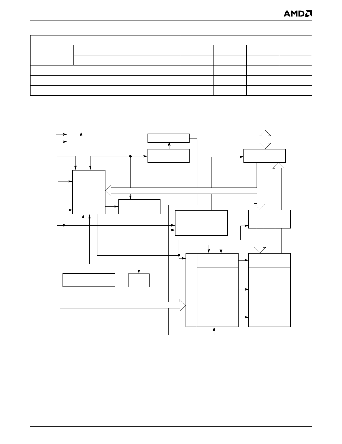
BLOCK DIAGRAM
DQ0
–
DQ7
Input/Output
Buffers
Data
Latch
V
CC
V
SS
RESET#
WE#
CE#
OE#
RY/BY#
State
Control
Command
Register
PGM Voltage
Generator
Sector Switches
Erase Voltage
Generator
Chip Enable
Output Enable
Logic
STB
A0–A18
VCC Detector
Timer
STB
Address Latch
Y-Decoder
X-Decoder
Y-Gating
Cell Matrix
21522A-1
Am29LV004 3
Page 4
CONNECTION DIAGRAMS
PRELIMINARY
A16
A15
A14
A13
A12
A11
A9
A8
WE#
RESET#
NC
RY/BY#
A18
A7
A6
A5
A4
A3
A2
A1
A17
V
SS
NC
NC
A10
DQ7
DQ6
DQ5
DQ4
V
CC
V
CC
NC
DQ3
DQ2
DQ1
DQ0
CE#
V
SS
CE#
A0
1
2
3
4
5
6
7
8
9
10
11
12
13
14
15
16
17
18
19
20
1
2
3
4
5
6
7
8
9
10
11
12
13
14
15
16
17
18
19
20
Standard TSOP
Reverse TSOP
40
39
38
37
36
35
34
33
32
31
30
29
28
27
26
25
24
23
22
21
40
39
38
37
36
35
34
33
32
31
30
29
28
27
26
25
24
23
22
21
A17
V
SS
NC
NC
A10
DQ7
DQ6
DQ5
DQ4
V
CC
V
CC
NC
DQ3
DQ2
DQ1
DQ0
OE#
V
SS
CE#
A0
A16
A15
A14
A13
A12
A11
A9
A8
WE#
RESET#
NC
RY/BY#
A18
A7
A6
A5
A4
A3
A2
A1
4 Am29LV004
21522A-2
Page 5
PRELIMINARY
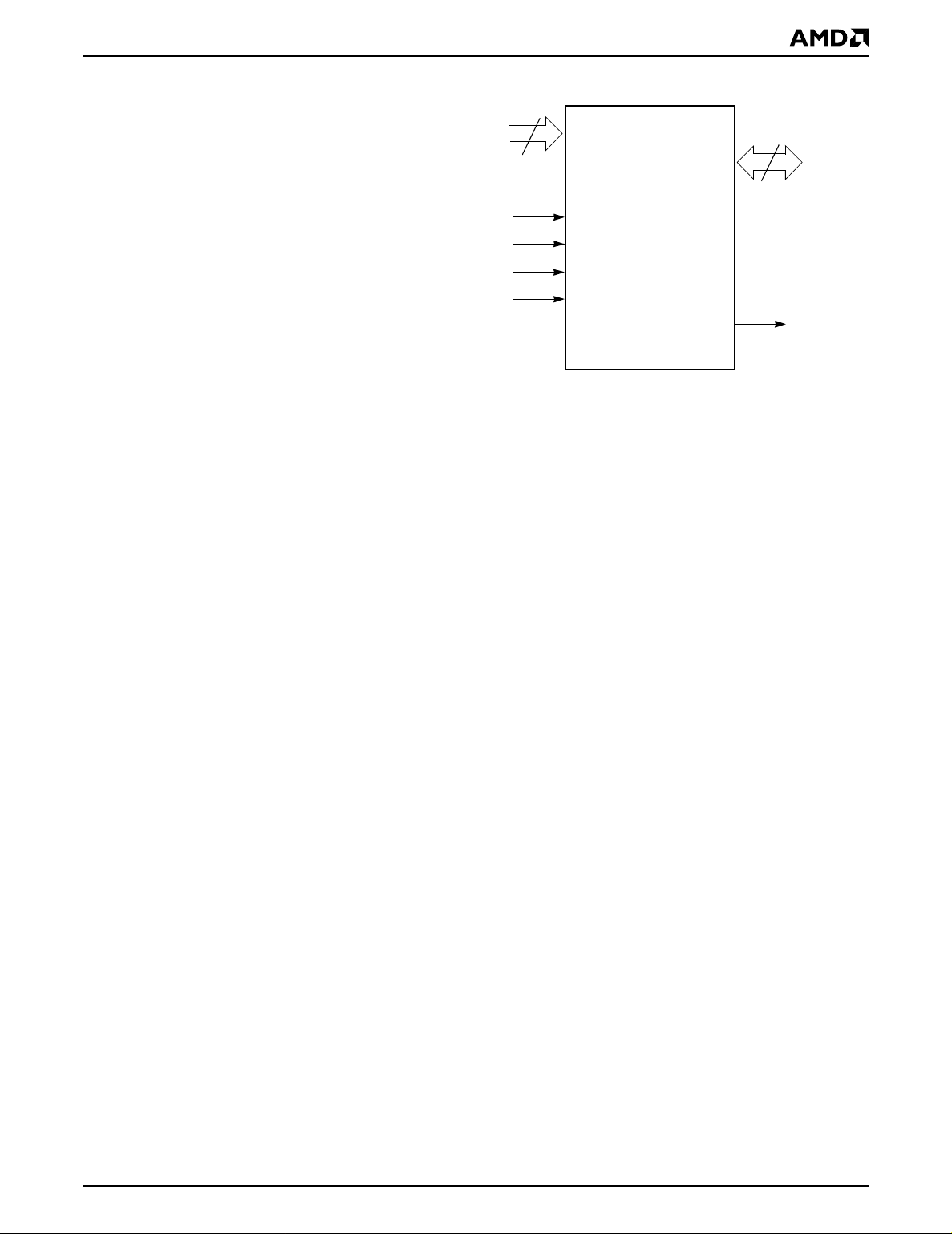
PIN CONFIGURATION
A0–A18 = 19 addresse s
DQ0–DQ7 = 8 data inputs/outputs
CE# = Chip enable
OE# = Output enable
WE# = Write enable
RESET# = Hardware reset pin, active low
RY/BY# = Ready/Busy# output
V
= 3.0 volt-only single power supply
CC
V
SS
NC = Pin not connected internally
(see Product Selector Guide for speed
options and voltage supply tolerances)
= Device ground
LOGIC SYMBOL
19
A0–A18
CE#
OE#
WE#
RESET#
8
DQ0–DQ7
RY/BY#
21522A-3
Am29LV004 5
Page 6
PRELIMINARY
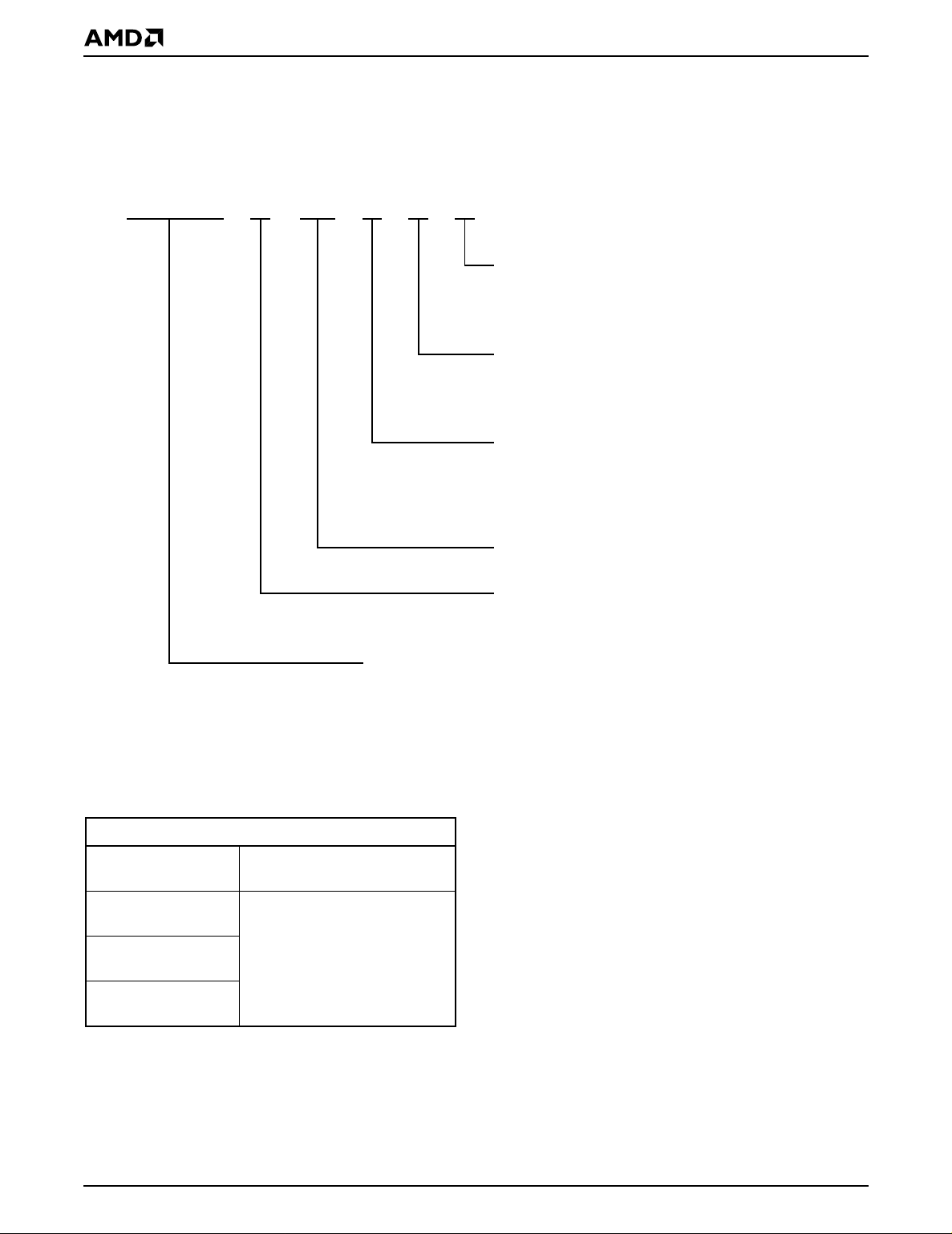
ORDERING INFORMATION
Standard Products
AMD sta nd ar d p rod ucts are av a il ab le i n seve ral packa ge s and opera ti ng ra ng es. The order nu mb er (Valid Co mb i nation) is formed by a combination of the elements below.
Am29LV004
-90R
CET
OPTIONAL PROCESSING
Blank = Standard Proces sing
B = Burn-in
(Contact an AMD representative for more information)
TEMPERATURE RANGE
C=Commercial (0°C to +70°C)
I = Industrial (–40°C to +85°C)
E = Extended (–55°C to +125°C)
PACKAGE TYPE
E = 40-Pin Thin Small Outline Package (TSOP)
Standard Pinout (TS 040)
F = 40-Pin Thin Small Outline Package (TSOP)
Reverse Pinout (TSR040)
SPEED OPTION
See Product Selector Guide and Valid Combinations
BOOT CODE SECTOR ARCHITECTURE
T = Top Sector
B = Bottom Sector
DEVICE NUMBER/DE SCRIP TION
Am29LV004
4 Megabit (512 K x 8-Bit) CMOS Flash Memory
3.0 Volt-only Read, Program, and Erase
Valid Combinations list configurations planned to be supported in volume for this device. Consult the local AMD sales
office to confirm availability of specific valid combinations and
to check on newly released combinations.
Am29LV004T-70R,
Am29LV004B-70R
Am29LV004T-80,
Am29LV004B-80
Am29LV004T-90,
Am29LV004B-90
Am29LV004T-120,
Am29LV004B-120
Valid Combinations
EC, EI, FC, FI
EC, EI, EE, FC, FI, FE
6 Am29LV004
Valid Combinations
Page 7
PRELIMINARY
DEVICE BUS OPERATIONS
This section describes the requirements and use of the
device bus operations, which are initiated through the
internal command register. The command register itself
does not occupy any addressable memo ry location.
The reg iste r is co mposed of lat che s that store the co mmands, along with the address and data information
needed to execu te the com mand . The co nte nts of th e
Table 1. Am29LV004 Device Bus Operations
Operation CE# OE# WE# RESET# Addresses (See Note) DQ0–DQ7
Read L L H H A
Write L H L H A
V
±
Standby
Output Disable L H H H X High-Z
Reset X X X L X High-Z
Temporary Sector Unprotect X X X V
Legend:
L = Logic Low = VIL, H = Logic High = VIH, VID = 12.0 ± 0.5 V, X = Don’t Care, AIN = Address In, DIN = Data In, D
Note: Addresses are A18–A0.
CC
0.3 V
XX
register serve a s input s to the inter nal sta te mac hine.
The state machine outputs dictate the function of the
device. Table 1 lists the devi ce bus op erat ions , the inputs and control levels they require, and the resulting
output. The following subsections describe eac h of
these operations in further detail.
D
D
D
= Data Out
OUT
OUT
VCC ±
0.3 V
ID
IN
IN
X High-Z
A
IN
IN
IN
Requirements for Reading Array Data
To read array dat a from the ou tputs, the sys tem must
drive the CE# and OE # pins to V
. CE# is the power
IL
control an d sel ects the de vice . OE# is th e outpu t control and gates array data to the output pins. WE#
should remain at V
.
IH
The internal state machine is set for reading array
data upon devic e power-up, or aft er a hardware re set .
This ensures that no spurious alteration of the memory content occurs during the power transition. No
command is necessary i n this mode to obtain array
data. Standard micropr ocessor read cycles that assert valid addresses on the device add ress inputs pr oduce valid data on the device data outputs. The
device remains enabled for read access unt il the command register contents are altered.
See “R ead ing Ar ray Data” fo r more info rmatio n. Refer
to the AC Read Operations table for timing specifications and to Figure 12 for the timing diagram. I
CC1
in
the DC Characteristics table represents the active current specification for reading array data.
Writing Commands/Command Sequences
To write a command or command sequence (which includes programming data to the device and erasing
sectors of memory ), the sy stem m ust drive WE# an d
CE# to V
, and OE# to VIH.
IL
An eras e op e ra tio n ca n er ase on e s ect or, multipl e se ctors, or the entire device. Tables 2 and 3 indicate the
address space that each sector occupies. A “sector address” cons ists of the address bits required to uniquely
select a sector. The “Command Defini tions” section
has details on erasing a sector or the entire chip, or
suspending/resuming the erase operation.
After the system writes the autoselect command sequence, the device enters the autoselect mode. The
system can th en re ad aut ose lect codes fr om th e inter nal register (which is separate from the memory array)
on DQ7– DQ0 . St anda rd r ead cycle ti ming s ap ply in this
mode. Re fer to th e “ Autosele ct Mo de” an d “ Au to select
Command Sequence” sections for more information.
I
in the DC Charac teristics table represents the ac-
CC2
tive current specification for the write mode. The “AC
Characteristics” section contains timing specification
tables and timing diagrams for write operations.
Program and Erase Operation Status
During an erase or program operation, the system may
check the status of the operation by reading the status
bits on DQ7–DQ0. Standard read cycle timings and I
read specificati ons apply. Refer to “Write Operation
Status” for more information, and to “AC Characteristics” for timing diagrams.
CC
Am29LV004 7
Page 8

PRELIMINARY
Standby Mode
When th e sy st em is not read ing or wr itin g to the dev ice,
it can place the device in the standby mode. In this
mode, current consumption is greatly reduced, and the
outputs are placed in the high impedance state, independent of the OE# input.
The dev ice en ter s t he CM OS st an dby mode wh en the
CE# and RESET# pins are both held at V
CC
± 0.3 V.
(Note th at thi s is a mor e res trict ed vol tage rang e tha n
V
.) If CE# and RESET# are held at VIH, but no t wit hin
IH
V
± 0.3 V, the device will be in the standby mode, but
CC
the standby current will be greater. The device requires
standard access time (t
) for read access when the
CE
device is i n e ith er of these st and by modes, before it is
ready to read data.
If the device i s desele cte d during erasur e or pro gram ming, the device draws active current until the
operation is completed.
In the DC C haracte ristic s tabl es, I
CC3
and I
CC4
repre-
sents the standby current specification.
Automatic Sleep Mode
The au tomatic sl eep mode m inimizes F lash devi ce
energy co nsumption. The device autom atically
enables this mode when addresses remain stable for
t
+ 30 ns. The automatic sleep mode is indepen-
ACC
dent of the CE # , WE #, an d O E # co ntr ol s i gn als. St an dard address access timings provide new data when
addresses are changed. While in sleep mode, output
data is latched and always available to the system. I
CC5
in the DC Characteristics table represents the automatic sleep mode current specification.
RESET#: Hardware Reset Pin
The RESET# pin provides a hardware method of resetting the device to reading array data. When the RE-
SET# pin is driven low for at least a per iod of t
RP
, the
device immediately terminates any operation in
progress, tristates all output pins, and ignores all
read/write commands for the duration of the RESET#
pulse. The device also resets the internal state machine to reading array data. The operation that was interrupted should be reinitiated once the device is ready
to accept another command sequence, to ensure data
integrity.
Current is reduced for the duration of the RESET #
pulse. When RESET# is held at V
draws CMOS standby current (I
at V
but no t wi t hin VSS±0.3 V, the standby current will
IL
±0.3 V, the device
SS
). If RESET# is held
CC4
be greater.
The RESET# pin may be tied to the system reset cir-
cuitry. A system rese t would thus also res et th e Flas h
memory, enabling the system to read the boot-up firmware from the Flash memory.
If RESET# is asserted during a program or erase operation, the RY/BY# pin remains a “0” (busy) until the
internal reset operation is complete, which requires a
time of t
(during Embedded Algorithms ). The
READY
system can thus m onitor RY/BY# to determine
whether the reset op erati on is c ompl ete. If R ESET # is
asserted when a prog ram or erase operati on is not ex ecuting (RY/BY# pin is “1”), the reset operation is
completed within a time of t
ded Algorithms). The system can read data t
the RESET# pin returns to V
(not during Embed-
READY
.
IH
RH
after
Refer to the AC Characteristics tables for RESET# parameters and to Figure 13 for the timing diagram.
Output Disable Mode
When the OE# input is at VIH, output from the device is
disabl e d . Th e o ut p ut pi n s ar e pl a c ed i n t he h igh i m pedance state.
8 Am29LV004
Page 9
PRELIMINARY
Table 2. Am29LV004T Top Boot Block Sector Address Table
Sector Size
Sector A18 A17 A16 A15 A14 A13
SA0 0 0 0 X X X 64 00000h-0FFFFh
SA1 0 0 1 X X X 64 10000h-1FFFFh
SA2 0 1 0 X X X 64 20000h-2FFFFh
SA3 0 1 1 X X X 64 30000h-3FFFFh
SA4 1 0 0 X X X 64 40000h-4FFFFh
SA5 1 0 1 X X X 64 50000h-5FFFFh
SA6 1 1 0 X X X 64 60000h-6FFFFh
SA7 1 1 1 0 X X 32 70000h-77FFFh
SA8 1 1 1 1 0 0 8 78000h-79FFFh
SA9 1 1 1 1 0 1 8 7A000h-7BFFFh
SA10 1 1 1 1 1 X 16 7C000h-7FFFFh
(Kbytes)
Address Range
(in hexadecimal)
Table 3. Am29LV004B Bottom Boot Block Sector Address Table
Sector Size
Sector A18 A17 A16 A15 A14 A13
SA0 0 0 0 0 0 X 16 00000h-03FFFh
SA1 0 0 0 0 1 0 8 04000h-05FFFh
SA2 0 0 0 0 1 1 8 06000h-07FFFh
SA3 0 0 0 1 X X 32 08000h-0FFFFh
SA4 0 0 1 X X X 64 10000h-1FFFFh
SA5 0 1 0 X X X 64 20000h-2FFFFh
SA6 0 1 1 X X X 64 30000h-3FFFFh
SA7 1 0 0 X X X 64 40000h-4FFFFh
SA8 1 0 1 X X X 64 50000h-5FFFFh
SA9 1 1 0 X X X 64 60000h-6FFFFh
SA10 1 1 1 X X X 64 70000h-7FFFFh
(Kbytes)
Address Range
(in hexadecimal)
Autoselect Mode
The autoselect mode provides manufacturer and device identification, and sector protection verification,
through identifier codes output on DQ7–DQ0. This
mode is primarily intended for programming equipment
to auto mati ca lly match a de vice to b e pr ogra mmed with
its corresponding programming al gorithm. However,
the aut osel ect co des can also be a cces sed in -sy stem
through the command register.
When using programming equipment, the autoselect
mode requires V
Address pins A6, A1, and A0 must be as shown in Table
4. In addition, when verifying sector protection, the sec-
(1 1.5 V to 12.5 V) on address pin A9.
ID
Am29LV004 9
tor address must appear on the appropriate highest
order address bits (see Tables 2 and 3). Table 4 shows
the remaining address bits that are don’t care. When all
necessary bits have been set as required, the programming equipment may then read the corresponding identifier code on DQ7–DQ0.
To access the autoselect codes in-system, the host
system can issue the autoselect command via the
command register, as shown in Table 5. This method
does not require V
. See “Command Definitions” for
ID
details on using the autoselect mode.
Page 10
PRELIMINARY
Table 4. Am29LV004 Autoselect Codes (High Voltage Method)
Description CE# OE# WE#
A18
to
A13
A12
to
A10 A9
A8
to
A7 A6
A5
to
A2 A1 A0
DQ7
to
DQ0
Manufacturer ID: AMD L L H X X V
Device ID: Am29LV004T
(Top Boot Block)
Device ID: Am29LV004B
(Bottom Boot Block)
Sector Protection Verification L L H SA X V
LLHXXV
LLHXXV
XLXLL 01h
ID
XLXLH B5h
ID
XLXLH B6h
ID
XLXHL
ID
L = Logic Low = VIL, H = Logic High = VIH, SA = Sector Address, X = Don’t care.
Sector Protection/Unprotection
The hardware sector protection feature disables both
program and erase operations in any sector. The hard-
SET# pin, all the previously protected sectors are
protected a gain. Figure 1 sh ows the algorithm, a nd
Figure 19 shows the timing diagrams, for this feature.
ware sector unprotection feature re-enables both program and eras e operat ions in p reviou sly prot ected
sectors.
The device is shipped with all secto rs unprotected .
AMD offers the option of progra mming and prote cting
sectors at its factory prior to shipping the device
through AMD’s ExpressFlash™ Service. Contact an
AMD representative for details.
It is p ossi ble t o det ermi ne wh ethe r a s ector is p rotec ted
or unprotected. See “Autoselect Mo de” for details.
START
RESET# = V
(Note 1)
Perform Erase or
Program Operations
ID
01h
(protected)
00h
(unprotected)
Sector protection/unprotection must be implemented
using programming equipment.The procedure requires
a high voltage (V
) on addr ess pin A9 a nd OE#. De -
ID
tails on this method are provided in a supplement, publicat ion n umbe r 20 874. Cont act an A MD re pre senta tive
to request a copy .
Temporary Sector Unprotect
This feature allows temporary unprotection of previously protected sectors to change data in-system. The
Sector U n pr ote ct m od e i s a cti va ted by s e tting th e R ESET# pin t o V
sector s can b e pr o gr amm ed or er as ed by s ele ct i ng t he
sector addres ses. Once V
. During thi s mod e, form erly pr otecte d
ID
is remove d fro m the RE -
ID
RESET# = V
Temporary Sector
Unprotect Completed
(Note 2)
Notes:
1. All protected sectors unprotected.
2. All previously protected sectors are protected once
again.
IH
21522A-4
Figure 1. Temporary Sector Unprotect Operation
10 Am29LV004
Page 11

PRELIMINARY
Hardware Data Protection
The command sequence requir ement of unlock cycle s
for programming or erasing provides data protection
against inadvertent writes (refer to Table 5 for command definitions). In addition, the following hardware
data protection measures prevent accidental erasure
or prog ramm ing, w hich m ig ht othe rwis e be ca use d by
spurious system level signals during V
power-up
CC
and power-down transition s, or from system noise.
Low V
When V
cept any write cycles. This protects data during V
Write I nhibit
CC
is less than V
CC
, the device does not ac-
LKO
CC
power-up and power-down. The command register and
all internal program/erase circuits are disabled, and the
device resets. Subsequent writes are ignored until V
is greater t han V
. The system must p rovide the
LKO
CC
proper signals to the control pins to prevent unintentional writes when V
is greater than V
CC
LKO
.
COMMAND DEFINITIONS
Writing specific ad dress and data commands or sequences into the command register initiates device operations. Table 5 defines the valid register command
sequences. W riting incor rect ad dress and da ta val-
ues or writing them in the improper sequence resets
the device to reading array data.
All addresses are latched on the falling edge of WE# or
CE#, whichever happens later. All data is latched on
the rising edge of WE# or CE#, whichever happens
first. Refer to the appropriate timing diagrams in the
“AC Characteristics” section.
Reading Array Data
The device is automatically set to reading array data
after d evice power- up. N o comm ands ar e requ ired t o
retrieve data. The device is also ready to read array
data after completing an Embedded Program or Embedded Erase algorithm.
After the device accepts an Erase Suspend command, the de vice enters the E rase Suspend m ode.
The system can read array data using the standard
read timings, except that if it reads at an address
within erase-susp ended sectors, the device outputs
status data. After completing a programming operation in the Erase Suspend mode, the system may
once again read array data with the same exception.
See “Erase Suspend/Erase Resume Commands” for
more information on this mode.
The syst em
able the device for reading array data if DQ5 goes high,
or while in the a utoselect mode. Se e the “R eset C om mand” section, next.
must
issue the reset command to re-en-
Write Pulse “Glitch” Protection
Noise pulses of less than 5 ns (typical) on OE#, CE# or
WE# do not initiate a write cycle.
Logical Inhibit
Write cycles are inhibited by holding any one of OE# =
V
, CE# = VIH or WE# = VIH. To initiate a writ e cycle,
IL
CE# and WE# must be a logical zero while OE# is a
logical one.
Power-Up Write Inhibit
If WE# = CE# = V
and OE# = VIH during po wer up, the
IL
device does not accept commands on the rising edge
of WE#. The internal state machine is automatically
reset to reading array data on power-up.
See also “Requirements for Reading Array Data” in the
“Devic e B u s Op er at io ns ” section f or m ore i n for ma tion.
The Read Operations table provides the read parameters, and Figure 12 shows the timing diagram.
Reset Command
Writing the reset command to the device resets the device to r ea di n g a rr ay da ta. A dd re ss bits ar e do n’t car e
for this command.
The reset command may be written between the sequence cycles in an erase command sequence before
erasing begins. This rese ts the device to reading array
data. Once erasure begins, however, the device ignores reset commands until t he operation is complete.
The reset command may be written between the sequence cycles in a program command sequence before programmi ng begins. This resets the device to
reading a rray data (a lso applie s to programm ing in
Erase Su spend mode ). Once p rogrammin g begins,
however, the device ignores r eset co m mand s until th e
operat ion i s comp l et e.
The reset command may be written between the sequence cycles in an autoselect command sequence.
Once in the autoselect mode, the reset command
be written to re turn to re ading ar ray data (also applies
to autoselect during Erase Suspend).
If DQ5 goes high during a program or erase operation,
writing the res et comm and r eturn s th e devic e to re ading array data (also applies during Erase Suspend).
must
Am29LV004 11
Page 12
PRELIMINARY
Autoselect Command Sequence
The autoselect comm and sequence allows the host
system to access the manufacturer and devices codes,
and determine whether or not a sector is protected.
Table 5 shows th e address and d ata requiremen ts.
This meth od is an alternati ve to th at sh own in Table 4,
which is intended for PROM programmers and requires
V
on address bi t A9.
ID
The auto sel e c t comm an d se qu enc e i s ini ti a te d by wr i ting two unlock cycles, followed by the autos elect com mand. The device then enters the autoselect mode,
and the s yste m may r ead at any addre ss any n um ber
of time s, witho ut initia ting ano ther comma nd sequen ce.
A read cycle at address XX00h retrieves the manufacturer code. A read cy cle a t address X X0 1h r eturn s th e
device code. A read cycle containing a sector address
(SA) and the address 02h returns 01h if that sector is
protect ed, or 00 h i f it is un pr ote cte d. R e fe r to Tables 2
and 3 for valid sector addresses.
The system must wr ite the reset comma nd to exit the
autoselect mode and return to reading array data.
Byte Program Command Sequence
Programming is a four-bus-cycle operation. The program command sequence is initiated by writing two unlock write cycles, followed by the program set-u p
comman d. T he pr ogra m ad dres s an d dat a are wr itten
next, which in turn initiate the Embedded Program a lgorithm. The system is
controls or timin gs. The device automat ically provides
intern ally ge ne r ated p r og ra m pu lse s a nd ve ri fy t h e pr ogrammed cell marg in. Table 5 shows the a ddre ss an d
data requirements for the byte program command sequence .
not
required to provide further
Programming is allowed in any sequence and across
sector boundaries. A bit cannot be programmed
from a “0” back to a “1”. Attempting to do so may halt
the oper ation and set DQ5 to “1”, or cau se the Data #
Polling algorithm to indicate the operation was successful. However, a succeeding read will show that the
data is still “0”. Only erase operations can convert a “0”
to a “1”.
Figure 2 illustrates the algorithm for the program operation. See the Erase/Program Operations table in “AC
Characteristics” for parameters, and to Figure 14 for
timing diagrams.
START
Write Program
Command Sequence
Data Poll
Embedded
algorithm
in progress
Increment Address
Program
No
from System
Verify Data?
Yes
Last Address?
No
When th e Embe dded Pr ogra m algor ithm is compl ete,
the devic e then returns to readi ng array data a nd addresses a re no l ong er latc hed. The sys tem can de termine the status of the program operation by using
DQ7, DQ6, or RY/BY#. See “Write Operation Status”
for information on these status bits.
Any commands written to the device during the Embedded Program Algorithm are ignored. Note that a
Note: See Table 5 for program command sequence.
hardware reset immediately t ermin ates the p rogram-
ming opera tion. The Byte Prog ram command sequence should be reinitiated once the device has reset
to reading array data, to ensure data integrity.
12 Am29LV004
Yes
Programming
Completed
21522A-4
Figure 2. Program Operation
Page 13

PRELIMINARY
Chip Erase Command Sequence
Chip erase is a six bus cycle operation. The chip erase
command s equence i s initiate d by writin g two unloc k
cycles, followed by a set-up command. Two additional
unlock wri t e cyc l es ar e t he n fo ll owe d by th e ch ip era se
command, which in turn invokes the Embedded Erase
algorithm. The device does
preprogram prior to erase. The Embedded Erase algorithm automatical ly preprograms and verifies t he entire
memo ry for an all zero d ata pa ttern prio r to ele ctric al
erase. The system is not required to pro vide any controls or timings during these operations. Table 5 shows
the addr ess and data requirem ents for the chip eras e
command sequence .
Any commands written to the chip during the Embedded Erase algorithm are ignored. Note that a hardware
reset during the chip erase operation immediately terminates the operation. The Chip Erase command sequence should be reinitiated once the device has
returned to reading array data, to ensure data integrity.
The syste m can deter mine the stat us of the e ras e operation by using DQ7, DQ6, DQ2, or RY/BY#. See
“Write Operation Status” for information on these status bits. When the Embedded Erase algorithm is complete, the device returns to reading array data and
addresses are no longer latched.
Figure 3 illustr ates the algor ithm for the e rase operation. See the E rase/P rog ram Ope ratio ns tabl es in “AC
Characteristics” for parameters, and to Figure 15 for
timing diagrams.
not
require the system to
Sector Erase Command Sequence
Sector erase is a six bus cycle operation. The sector
erase command sequence is i nitiated by writing two
unlock c ycl es , f o ll owed by a s et- up co mm an d. Two additional unlock write cycles are then followed by the address o f th e sector to be er ase d, an d the sec tor e ras e
command. Table 5 shows the addre ss and data requirements for the sector erase command sequence.
The device does
the memory prior to erase. The Embedded Erase algorithm automatically programs and verifies the sector for
an all zero data pattern prior to electrical erase. The
system is not required to provide any controls or timings during these operations.
After the command sequence is written, a sector erase
time-out of 50 µs begins. During the time-out period,
additi onal secto r addresses and secto r erase com mands may be written. Loading the sector erase buffer
may be done in any sequence, and the number of sectors may be from one sector to all sectors. The time between th es e add it i onal cyc l e s must be less th an 50 µs,
otherwise the last address and command might not be
accepted , and era sur e ma y beg in. It i s re comm ende d
not
require the system to preprogram
that processor interrupts be disabled during this time to
ensure all commands are accepted. The interrupts can
be re-e nabled after the la st Sec tor Er ase com man d is
written. If the time between additional sector erase
commands can be assumed to be less than 50 µs, the
system need not monitor DQ3. Any command other
than Sector Erase or Erase Suspend during the
time-out period resets the device to reading array
data. The system must rewrite the command sequence
and any additional sector addresses and commands.
The system can monitor DQ3 to determine if the sector
erase timer has timed out. (See the “DQ3: Sector
Erase T imer” sectio n.) The t ime-out begins f rom the ri sing edge of the final WE# pulse in the command sequence .
Once the sector erase operation has begun, only the
Erase Sus p en d co mma nd is v al id. A ll o the r c o mman ds
are ignored. Note that a hardware reset during the
sector er as e op er atio n i m me diately ter min ate s the op eration . Th e S ec tor E ras e c o mm an d sequenc e sh ou l d
be reinitiated once the device has retu rned to rea ding
array data, to ensure data integrity.
When the Embedded Erase algorithm is complete, the
device returns to reading array data and addresses are
no longer latch ed. The system can determ ine the sta tus of the erase operation by using DQ7, DQ6, DQ2, or
RY/BY #. ( Ref er t o “W rit e Oper ati on Stat us” for i nfo rmation on these status bits.)
Figure 3 illustr ates the algor ithm for the e rase operation. Refer to the Era se/Progra m Operat ions table s in
the “AC Characteristics” section for parameters, and to
Figure 15 for timing diagrams.
Erase Suspend/Erase Resume Commands
The Erase Suspend command allow s the system to interrupt a sector e rase operation a nd then read data
from, or program data to, any sector not selected for
erasure. This command is valid only during the sector
erase operation, including the 50 µs time-out period
during the sector erase command sequence. The
Erase Suspend command is ignored if written during
the chip eras e o pera tion o r Em bedd ed P rogr am a lgorithm. Writing the Erase Suspend command during the
Sector Erase time-out immediately terminates the
time-out period and suspends the erase operation. Addresses are “don’ t- car es” w he n w ri tin g the Eras e Suspend command.
When the Era s e Su sp end c o mma nd is written du ring a
sector erase operation, the device requires a maximum
of 20 µs to su spend the er ase operation. H owever,
when the Erase Suspend command is written during
the sector erase tim e-out, th e device imm ediate ly terminates the time-out period and suspends the erase
operat ion.
Am29LV004 13
Page 14

PRELIMINARY
After the eras e operation has been su spended, the
system can read array data from or program data to
any sector not selected for erasure. (The device “erase
suspends” all sec tors selected for erasure.) N ormal
read and write timings and command definitions apply.
Reading at any address within erase-suspended sectors produces status data on DQ7–DQ0. The system
can use D Q7 , or DQ6 and DQ2 toge th er, to deter mi n e
if a sector is actively erasing or is erase-suspended.
See “Write Op eration St atus” for informat ion on thes e
status bits.
After an erase-suspended program operation is complete, the system can once again read array data within
non-suspended sectors. The system can determine the
status of the program operation using the DQ7 or DQ6
status bits, just as in the standard program operation.
See “Write Operation Status” for more information.
The system may also write the autoselect command
sequence when the device is in the Erase Suspend
mode. The device allows r eading autoselect codes
even at addresses within erasing s ectors, since the
codes are not stored in the memory array. When the
device exits the autoselect mode, the device reverts to
the Erase Su spend mode, an d is ready for ano ther
valid op er ati o n. Se e “A ut os e lec t Comm an d Se qu en c e”
for more information.
The system must write the Erase Resume command
(address bits are “don’t care”) to exit the erase suspend
mode an d co nt in ue th e se ct or e ra se op era ti on. Fu rt h er
writes of the Re sume comman d are ig nored. A nothe r
Erase Suspend command can be written after the device has resumed erasing.
START
Write Erase
Command Sequence
Data Poll
from System
No
Notes:
1. See Table 5 for erase command sequence.
2. See “DQ3: Sector Erase Timer” for more information.
Data = FFh?
Yes
Erasure Completed
Embedded
Erase
algorithm
in progress
21522A-5
Figure 3. Erase Operatio n
14 Am29LV004
Page 15

PRELIMINARY
Table 5. Am29LV004 Command Definitions
Command
Sequence
(Note 1)
Read (Note 5) 1 RA RD
Reset (Note 6) 1 XXX F0
Manufacturer ID 4 555 AA 2AA 55 555 90 X00 01
Autoselect
(Note 7)
Program 4 555 AA 2AA 55 555 A0 PA PD
Chip Erase 6 555 AA 2AA 55 555 80 555 AA 2AA 55 555 10
Sector Erase 6 555 AA 2AA 55 555 80 555 AA 2AA 55 SA 30
Erase Suspend (Note 9) 1 XXX B0
Erase Resume (Note 10) 1 XXX 30
Device ID, Top Boot Block 4 555 AA 2AA 55 555 90 X01 B5
Device ID, Bottom Boot Block 4 555 AA 2AA 55 555 90 X01 B6
Sector Protect V erif y
(Note 8)
First Second Third Fourth Fifth Sixth
Addr Data Addr Data Addr Data Addr Data Addr Data Addr Data
Cycles
4 555 AA 2AA 55 555 90
Legend:
X = Don’t care
RA = Address of the memory location to be read.
RD = Data read from location RA during read operation.
PA = Address of the memory location to be programmed.
Addresses latch on the falling edge of the WE# or CE# pulse,
whichever happens later.
Bus Cycles (Notes 2-4)
(SA)
X02
00
01
PD = Data to be programmed at location P A. Data latches on the
rising edge of WE# or CE# pulse, whichever happens first.
SA = Address of the sector to be verified (in autoselect mode) or
erased. Address bits A18–A13 uniquely select any sector.
Notes:
1. See Table 1 for description of bus operations.
2. All values are in hexadecimal.
3. Except when reading array or autoselect data, all
commandbus cycles are write operations.
4. Address bits A18–A11 are don’t cares for unlock and
command cycles.
5. No unlock or command cycles required when reading array
data.
6. The Reset command is required to return to reading array
data when device is in the autoselect mode, or if DQ5 goes
high (while the device is providing status data).
7. The fourth cycle of the autoselect command sequence is a
read cycle.
8. The data is 00h for an unprotected sector and 01h for a
protected sector. See “Autoselect Command Sequence” for
more information.
9. The system may read and program in non-erasing sectors, or
enter the autoselect mode, when in the Erase Suspend
mode. The Erase Suspend command is valid only during a
sector erase operation.
10. The Erase Resume command is valid only during the Erase
Suspend mode.
Am29LV004 15
Page 16

PRELIMINARY
WRITE OPERATION STATUS
The device provides several bits to determine the status of a write op eratio n: DQ2, DQ 3, DQ5, DQ6 , DQ7,
and RY/BY#. Table 6 and the following subsections describe the functions of these bits. DQ7, RY/BY#, and
DQ6 each offer a method for determining whether a
program or erase operation is complete or in progress.
These three bits are discussed first.
Ta ble 6 show s the outputs fo r Data# Polling o n DQ7.
Figure 4 shows the Data# Polling algorithm.
START
DQ7: Data# Polling
The Data# Polling bit, DQ7, indicates to the host s ystem
whether an Embedded Algorithm is in progress or completed, or whether th e device is in Erase Suspen d.
Data# Polling is valid after the rising edge of the final
WE# pulse in the program or erase command sequence.
During the Embedded Program algorithm, the device
outputs on DQ7 the c ompleme nt of the da tum programmed to DQ7. This DQ7 status also applies to programming during Erase Suspend. When the
Embedde d Pro gram al gorith m is co mplete , the devic e
outputs the datum programmed to DQ7. The system
must provide the program address to read valid status
information on DQ7. If a program address falls within a
protected sector, Data# Polling on DQ7 is active for approximately 1 µs, then the device returns to reading
array data.
During the Embedded Erase algorithm, Data# Polling
produces a “0” on DQ7. When the Embedded Erase algorithm is comp lete, o r if the de vice en ters t he Erase
Suspend mode, Data# Polling produces a “1” on DQ7.
This is analogous to the complement/true datum output
described for the Embedded Program algorithm: the
erase function changes all the bits in a sector to “1”;
prior to this, the device outputs the “complement,” or
“0.” The system must provide an address within any of
the sectors selected for erasure to read valid status information on DQ7.
No
Read DQ7–DQ0
Addr = VA
DQ7 = Data?
No
DQ5 = 1?
Yes
Read DQ7–DQ0
Addr = VA
DQ7 = Data?
No
FAIL
Yes
Yes
PASS
After an erase command sequence is written, if all sectors selected for erasing are protected, Data# Polling
on DQ7 is active for approximately 100 µs, then the de-
Notes:
1. VA = Valid address for programming. During a sector
vice returns to reading array data. If not all selected
sectors are protected, the Embedded Erase algorithm
erases the unprotected sectors, and ignores the selected sectors that are protected.
2. DQ7 should be rechecked even if DQ5 = “1” because
When the sys tem det ects DQ7 h as changed from the
complement to true data, it can read valid data at DQ7–
DQ0 on t h e
following
read cycles. This is because DQ7
may change asynchronously with DQ0–DQ6 while
Output Enable (OE#) is asserted low. Figure 16, Data#
Polling Timings (During Embedded Algorithms), in the
“AC Characteristics” section illustrates this.
16 Am29LV004
erase operation, a valid address is an address within any
sector selected for erasure. During chip erase, a valid
address is any non-protected sector address.
DQ7 may change simultaneously with DQ5.
21522A-6
Figure 4. Data# Polling Algorithm
Page 17

PRELIMINARY
RY/ BY#: Read y/Bu sy#
The RY/BY# is a dedicated, open-drain output pin that
indicates whether an Embedded Algorithm is in
progress or complete. The RY/BY# status is valid after
the rising edge of the f inal WE# pulse in the command
sequence. Since RY/BY# is an open-drain output, several RY/BY# pins can be tied together in parallel with a
pull-up resistor to V
If the output is low (Busy), the device is actively erasing
or programming. (T his includes programm ing in the
Erase Suspend mode.) If the output is high (Ready),
the device is ready to read array data (including during
the Erase Suspend mode), or is in the standby mode.
Table 6 shows the outputs for RY/BY#. Figures 12, 13,
14 and 15 shows RY/BY# for read, reset, program, and
erase operations, respectively.
CC
.
DQ6: Toggle Bit I
Toggle Bit I on DQ6 indicates whether an Embedded
Progra m or Era se alg ori thm is i n progre ss or comple te,
or whether the device has entered the Erase Suspend
mode. Toggle Bit I may be read at an y address, and i s
valid aft er th e risi n g ed ge of the fin al WE # pu l se in th e
command sequence (prior to the program or erase operati on), and duri ng the sector erase time-out.
During an Embe dded Prog ram or Eras e algor ithm op eration, succe ssive read cycles to any a ddress c ause
DQ6 to toggle. (The system may use either OE# or
CE# to control the read cycles.) When the operation is
complete, DQ6 stops toggling.
Table 6 shows the ou tputs for Toggle Bit I on DQ6.
Refer to Figure 5 for the toggle bit algorithm, and to Figure 17 in t h e “ AC Ch ar ac ter i s ti cs” s ec ti o n fo r th e t og gle
bit timing diagrams. Figure 18 shows the differences
between DQ2 and DQ6 in graphical form. See also the
subsection on “DQ2: Toggle Bit II”.
DQ2: Toggle Bit II
The “Toggle Bit II” on DQ2, when used with DQ6, indicates whether a particular sector is actively erasi ng
(that is, the Embedded Erase algorithm is in progress),
or whet her t hat secto r is eras e-sus pen ded. Toggle B it
II is valid after the rising edge of the final WE# pulse in
the command sequence.
DQ2 toggles when the system reads at addresses
within those sectors that have been selected for erasure. (The syste m may use eith er OE # or CE # to con trol the read cycles.) But DQ2 cann ot distinguish
whether the sector is activ ely erasin g or is erase- suspended. DQ6, by comparison, indicates whether the
device is actively erasing, or is in Erase Suspend, but
cannot distinguish which sectors are selected for erasure. Thus, both status bits are required for sector and
mode information. Refer to Table 6 to compare outputs
for DQ2 and DQ6.
Figure 5 shows the toggle bit algorithm i n flowchart
form, and th e section “ D Q2 : Toggle Bit II” e x p lains the
algorithm. See also the “DQ6: Toggle Bit I” subsection.
Figure 17 sh ows the toggl e bit tim ing d iagram . Fi gur e
18 shows the differences between DQ2 and DQ6 in
graphical form.
After an erase command sequence is written, if all sectors selected for erasing are protected, DQ6 toggles for
approximately 100 µs, then returns to reading array
data. If n ot all selected se ctors are pro te cted , the E m bedded Erase algorithm erases the unprotected sectors, and ignores the selected sectors that are
protect ed.
The system can use DQ6 an d DQ2 togethe r to determine whether a sector is actively erasing or is erasesuspended. When the device is actively erasing (that
is, th e Em be dd e d Er as e alg or i t hm is i n pr og re s s ), D Q6
toggles. When the device enters the Erase Suspend
mode, DQ6 stop s to ggling . Ho wever, the system must
also use DQ2 to deter mine whic h sector s are eras ing
or erase-suspende d. Alter na tively, the system can use
DQ7 (see the subsection on “DQ7: Data# Polling”).
If a program address falls within a protected sector,
DQ6 togg les f or ap proxi mat ely 2 µs afte r the prog ram
comman d s eq uence is wr it ten , th en returns to r ea di n g
array data.
DQ6 also toggles during the erase-suspend-program
mode, and sto ps toggling once the E mbedded Program algorithm is complete.
Reading Toggle Bits DQ6/DQ2
Refer to Figure 5 for the following discussion. Whenever
the system initially begins reading toggle bit status, it
must read DQ7–DQ0 at least twice in a row to determine
whether a toggle bit is toggling. Typically, the system
would note and store the value of the toggle bit after the
first read. After the second read, the system would compare the new value of the toggle bit with the first. If the
toggle bit is not toggling, the device has completed the
program or erase operation. The system can read array
data on DQ7–DQ0 on the following read cycle.
However, if after the initial two read cycles, the system
determines that t he toggle bit is still toggling, t he sys tem also should note whether the value of DQ5 is high
(see the section on DQ5). If it is, the system should
then determine again whether the toggle bit is toggling,
since the toggle bi t ma y h av e s top ped toggli ng ju s t a s
DQ5 went high. If the toggle bit is no longer toggling,
the device has su cce ssfu lly comp let ed the prog ram o r
erase operation. If it is still t oggling, t he de vice did not
completed the operation successfully, and the system
must write the reset command to return to reading
array data.
Am29LV004 17
Page 18

PRELIMINARY
The remaining sc enario is that the system initially de termi n es th at th e tog gl e b it i s to gg l i ng a nd D Q 5 ha s n ot
gone high. The system may continue to monitor the
toggle bit and DQ5 through successive read cycles, determining t he stat us as described in th e previ ous paragraph. Alternatively, it may choose to perform other
system tasks. In this case, the system must start at the
beginning of the algorithm when it returns to determine
the status of the operation (top of Figure 5).
START
Read DQ7–DQ0
(Note 1)
Read DQ7–DQ0
No
(Notes
1, 2)
No
Program/Erase
Operation Complete
No
Toggle Bit
= Toggle?
Yes
DQ5 = 1?
Yes
Read DQ7–DQ0
Twice
Toggle Bit
= Toggle?
Yes
Program/Erase
Operation Not
Complete, Write
Reset Command
DQ5: Exceeded Timing Limits
DQ5 indi ca te s w h eth er th e p ro gr am or e ra se t i me ha s
exceeded a specified in ternal pulse count lim it. Under
these co ndi tions DQ5 p roduc es a “1.” This i s a fa ilur e
condition that indicates the program or erase cycle was
not successfully completed.
The DQ5 failure condition may appear i f the system
tries to program a “1” to a location that is previously
programmed to “0.” Only an erase operation can
change a “0 ” back to a “ 1.” Un der this condition, the
device halts the operation, and when the operation has
exceeded the timing limits, DQ5 produces a “1.”
Under both these conditions, the system must issue
the reset command to return the device to reading
array data.
DQ3: Sector Erase Timer
After writing a sector erase command sequence, the
system may read DQ3 to determine whether or not an
erase operation has begun. (The sector erase ti mer
does not apply to the chip erase command.) If additional
sectors are selected for erasure, the entire time-out also
applies after each additional sector erase command.
When the time-out is comp lete, DQ3 switches from “0”
to “1.” The system may ignore DQ3 if the system can
guarantee that the time between additional sector
erase commands will always be less than 50 µs. See
also the “Sector Erase Command Sequence” section.
After the sector erase command sequence is written,
the sys t em shou l d re ad th e s t at us o n D Q7 ( Da t a# Pol ling) or DQ6 (Toggle Bit I) to ensure the device has accepted the command sequence, and then read DQ3. If
DQ3 is “1”, the internally controlled erase cycle has begun; all fur t he r c omman ds (o t her t ha n Era s e Sus p en d)
are ignored until the erase opera tion is complete. If
DQ3 is “0”, the device will accept additional se ctor
erase commands. To ensure the command has been
accepted, the system software should check the status
of DQ3 prio r to and f ollo wing each su bsequ ent se cto r
erase c omman d. If DQ3 is high on the s econd status
check, the last command might not have been accepted. Table 6 shows the outputs for DQ3.
Notes:
1. Read toggle bit twice to determine whether or not it is
toggling. See text.
2. Recheck toggle bit because it may stop toggling as DQ5
changes to “1” . See text.
21522A-7
Figure 5. Toggle Bit Algorithm
18 Am29LV004
Page 19

PRELIMINARY
Table 6. Write Operation Status
DQ7
Standard
Mode
Erase
Suspend
Mode
Operation
Embedded Program Algorithm DQ7# Toggle 0 N/A No toggle 0
Embedded Erase Algorithm 0 Toggle 0 1 Toggle 0
Reading within Erase
Suspended Sector
Reading within Non-Erase
Suspended Sector
Erase-Suspend-Program DQ7# Toggle 0 N/A N/A 0
(Note 2) DQ6
1 No toggle 0 N/A Toggle 1
Data Data Data Data Data 1
Notes:
1. DQ5 switches to ‘1’ when an Embedded Program or Embedded Erase operation has exceeded the maximum timing limits.
See “DQ5: Exceeded Timing Limits” for more information.
2. DQ7 and DQ2 require a valid address when reading status information. Refer to the appropriate subsection for further details.
DQ5
(Note 1) DQ3
DQ2
(Note 2) RY/BY#
Am29LV004 19
Page 20

PRELIMINARY
ABSOLUTE MAXIMUM RATINGS
Storage Temperature
Plastic Packages . . . . . . . . . . . . . . . –65°C to +150°C
Ambient Temperature
with Power Applied . . . . . . . . . . . . . –65°C to +125°C
Voltage with Respect to Ground
V
(Note 1) . . . . . . . . . . . . . . . . .–0.5 V to +4.0 V
CC
A9, OE#,
and RESET# (Note 2). . . . . . . . .–0.5 V to +12.5 V
All other pins
(Note 1). . . . . . . . . . . . . . . . . –0.5 V to V
Output Short Circuit Current (Note 3) . . . . . . 200 mA
Notes:
1. Minimum DC voltage on input or I/O pins is –0.5 V. During
voltage transitions, input or I/O pins may undershoot V
to –2.0 V for periods of up to 20 ns. See Figure 6.
Maximum DC voltage on input or I/O pins is V
During voltage transitions, input or I/O pins may overshoot
to V
+2.0 V for periods up to 20 ns. See Figure 7.
CC
2. Minimum DC input voltage on pins A9, OE#, and RESET#
is –0.5 V. During voltage transitions, A9, OE#, and
RESET# may undershoot V
to 20 ns. See Figure 6. Maximum DC input voltage on pin
A9 is +12.5 V which may overshoot to 14.0 V for periods
up to 20 ns.
3. No more than one output may be shorted to ground at a
time. Duration of the short circuit should not be greater
than one second.
Stresses above those listed under “Absolute Maximum
Ratings” may cause permanent damage to the device. This is
a stress rating only; functional operation of the device at
these or any other conditions above those indicated in the
operational sections of this data sheet is not implied.
Exposure of the device to absolute maximum rating
conditions for extended periods may affect device reliability.
to –2.0 V for periods of up
SS
CC
+0.5 V.
CC
+0.5 V
SS
20 ns
+0.8 V
–0.5 V
–2.0 V
20 ns
20 ns
21522A-8
Figure 6 . Maximum Negative Overshoot
V
CC
+2.0 V
V
CC
+0.5 V
2.0 V
Waveform
20 ns
20 ns
20 ns
21522A-9
Figure 7. Maximum Positive Overshoot
Waveform
OPERATING RANGES
Commercial (C) Devices
Ambient Temperature (T
Industrial (I) Devices
Ambient Temperature (T
Extended (E) Devices
Ambient Temperature (T
V
Supply Voltages
CC
V
for regulated voltage range. . . . . . .3.0 V to 3.6 V
CC
V
for full voltage range. . . . . . . . . . . .2.7 V to 3.6 V
CC
Operating ranges define those limits between which the functionality of the device is guaranteed.
20 Am29LV004
) . . . . . . . . . . . 0°C to +70°C
A
) . . . . . . . . . –40°C to +85°C
A
) . . . . . . . . –55°C to +125°C
A
Page 21

PRELIMINARY
DC CHARACTERISTICS
CMOS Compatible
Parameter Description Test Conditions Min Typ Max Unit
V
= VSS to VCC,
IN
V
= VCC
CC
= VSS to VCC,
V
OUT
V
= V
CC
CE# = V
max
; A9 = 12.5 V 35 µA
CC max
CC max
5 MHz 10 16
OE#
IL,
= VIH
1 MHz 2 4
±1.0 µA
±1.0 µA
I
I
I
CC1
I
LIT
LO
LI
Input Load Current
A9 Input Load Current VCC = V
Output Leakage Current
VCC Active Read Current
(Note 1)
mA
VCC Active Write Current
(Notes 2 and 4)
VCC Standby Current
VCC Standby Current During Reset
Automatic Sleep Mode (Note 3)
CE# = V
V
CC
= V
OE#
IL,
CC max
= VIH
;
CE#, RESET# = V
V
= V
CC
RESET# = V
= V
V
IH
V
= V
IL
CC max
CC
± 0.3 V
SS
;
± 0.3 V
SS
± 0.3 V;
CC
±0.3 V
Input Low Voltage –0.5 0.8 V
Input High Voltage 0.7 x V
Voltage for Autoselect and
Temporary Sector Unprotect
Output Low Voltage IOL = 4.0 mA, VCC = V
Output High Voltage
Low VCC Lock-Out Voltage (Note
4)
= 3.3 V 11.5 12.5 V
V
CC
0.45 V
CC min
I
= –2.0 mA, VCC = V
OH
IOH = –100 µA, VCC = V
CC min
CC min
0.85 V
VCC–0.4
2.3 2.5 V
V
V
V
I
CC2
I
CC3
I
CC4
I
CC5
V
V
V
V
IL
IH
ID
OL
OH1
OH2
LKO
Notes:
1. The I
2. I
current listed is typically less than 2 mA/MHz, with OE# at VIH. Typical VCC is 3.0 V.
CC
active while Embedded Erase or Embedded Program is in progress.
CC
3. Automatic sleep mode enables the low power mode when addresses remain stable for t
4. Not 100% tested.
CC
CC
ACC
20 30 mA
0.2 5 µA
0.2 5 µA
0.2 5 µA
VCC + 0.3 V
V
+ 30 ns.
Am29LV004 21
Page 22

PRELIMINARY
DC CHARACTERISTICS (Contin ued)
Zero Power Flash
25
20
15
10
Supply Current in mA
5
0
0 500 1000 1500 2000 2500 3000 3500 4000
Time in ns
Note: Addresses are switching at 1 MHz
Figure 8. I
Current vs. Time (Showing Active and Automatic Sleep Currents)
CC1
15
10
5
Supply Current in mA
0
1 2345
3
Frequency in MHz
V
6
.
V
7
.
2
21522A-10
Note: T = 25 °C
Figure 9. Typical I
CC1
22 Am29LV004
21522A-11
vs. Frequency
Page 23

TE S T CONDITIONS
Device
Under
Test
C
L
6.2 kΩ
PRELIMINARY
3.3 V
2.7 kΩ
Output Load 1 TTL gate
Output Load Capacitance, C
(including jig capacitance)
Input Rise and Fall Times 5 ns
Input Pulse Levels 0.0–3.0 V
Table 7. Test Spe cifications
-90R,
Test Condition
-100
L
-120,
-150 Unit
30 100 pF
Note: Diodes are IN3064 or equivalent
Figure 10 . Test Se tup
KEY TO SWITCHING WAVEFORMS
WAVEFORM INPUTS OUTPUTS
Don’t Care, Any Change Permitted Changing, State Unknown
Does Not Apply Center Line is High Impedance State (High Z)
21522A-12
Input timing measurement
reference levels
Output timing measurement
reference levels
Steady
Changing from H to L
Changing from L to H
1.5 V
1.5 V
KS000010-PAL
3.0 V
0.0 V
1.5 V 1.5 V
Figure 11. Input Waveforms and Measurement Level s
Am29LV004 23
OutputMeasurement LevelInput
21522A-13
Page 24

AC CHARACTERISTICS
Read Operations
PRELIMINARY
Parameter
JEDEC Std Test Setup
t
AVAV
t
AVQV
t
ELQV
t
GLQV
t
EHQZ
t
GHQZ
t
Read Cycle Time (Note 1) Min 90 100 120 150 ns
RC
t
Address to Output Delay
ACC
t
Chip Enable to Output Delay OE# = V
CE
t
Output Enable to Output Delay Max 40 40 50 55 ns
OE
t
Chip Enable to Output High Z (Note 1) Max 30 30 30 40 ns
DF
t
Output Enable to Output High Z (Note 1) Max 30 30 30 40 ns
DF
Description
CE# = V
OE# = V
IL
IL
IL
Read Min 0 ns
Output Enable
t
OEH
Hold Time (Note 1)
Toggle and
Data# Polling
t
AXQX
Output Hold Time From Addresses, CE# or
t
OH
OE#, Whichever Occurs First (Note 1)
Notes:
1. Not 100% tested.
2. See Figure 10 and Table 7 for test specifications.
t
RC
Speed Option
-90R -100 -120 -150 Unit
Max 90 100 120 150 ns
Max 90 100 120 150 ns
Min 10 ns
Min 0 ns
Addresses
CE#
OE#
WE#
Outputs
RESET#
RY/BY#
0 V
Addresses Stable
t
ACC
t
OE
t
OEH
t
CE
HIGH Z
Output Valid
Figure 12. Read Operations Timings
t
OH
t
DF
HIGH Z
21522A-14
24 Am29LV004
Page 25

AC CHARACTERISTICS
Hardware Reset (RESET#)
Parameter
PRELIMINARY
Description All Speed OptionsJEDEC Std Test Setup Unit
t
READY
t
READY
RESET# Pin Low (During Embedded
Algorithms) to Read or Write (See Note)
RESET# Pin Low (NOT During Embedded
Algorithms) to Read or Write (See Note)
t
RESET# Pulse Width Min 500 ns
RP
t
RESET# High Time Before Read (See Note) Min 50 ns
RH
t
RESET# Low to Standby Mode Min 20 µs
RPD
t
RY/BY# Recovery Time Min 0 ns
RB
Note: Not 100% tested.
RY/BY#
CE#, OE#
RESET#
t
RP
t
Ready
Max 20 µs
Max 500 ns
t
RH
RY/BY#
CE#, OE#
RESET#
Reset Timings NOT during Embedded Algorithms
Reset Timings during Embedded Algorithms
t
Ready
t
RP
Figure 13. RESET# Timings
t
RB
21522A-15
Am29LV004 25
Page 26

AC CHARACTERISTICS
Erase/Program Operations
Parameter
PRELIMINARY
-90R -100 -120 -150JEDEC Std Description Unit
t
AVAV
t
AVWL
t
WLAX
t
DVWH
t
WHDX
t
GHWL
t
ELWL
t
WHEH
t
WLWH
t
WHWL
t
WHWH1tWHWH1
t
WHWH2tWHWH2
t
WC
t
AS
t
AH
t
DS
t
DH
t
OES
t
GHWL
t
CS
t
CH
t
WP
t
WPH
t
VCSVCC
t
RB
t
BUSY
Write Cycle Time (Note 1) Min 90 100 120 150 ns
Address Setup Time Min 0 ns
Address Hold Time Min 50 50 50 65 ns
Data Setup Time Min 50 50 50 65 ns
Data Hold Time Min 0 ns
Output Enable Setup Time Min 0 ns
Read Recovery Time Before Write
(OE# High to WE# Low)
Min 0 ns
CE# Setup Time Min 0 ns
CE# Hold Time Min 0 ns
Write Pulse Width Min 50 50 50 65 ns
Write Pulse Width High Min 30 30 30 35 ns
Programming Operation (Note 2) Typ 9 µs
Sector Erase Operation (Note 2) Typ sec
Setup Time (Note 1) Min 50 µs
Recovery Time from RY/BY# Min 0 ns
Program/Erase Valid to RY/BY# Delay Min 90 ns
Notes:
1. Not 100% tested.
2. See the “Erase and Programming Performance” section for more information.
26 Am29LV004
Page 27

AC CHARACTERISTICS
Program Command Sequence (last two cycles)
PRELIMINARY
Read Status Data (last two cycles)
Addresses
CE#
OE#
WE#
Data
RY/BY#
V
CC
t
VCS
t
WC
555h
t
GHWL
t
CS
t
WP
t
DS
A0h
t
AS
PA PA
t
AH
t
CH
t
WHWH1
t
WPH
t
DH
PD
t
BUSY
PA
Status
D
OUT
t
RB
Note: PA = program address, PD = program data, D
Figure 14. Program Operation Timings
is the true data at the program address.
OUT
21522A-16
Am29LV004 27
Page 28

AC CHARACTERISTICS
Erase Command Sequence (last two cycles) Read Status Data
PRELIMINARY
Addresses
CE#
OE#
WE#
Data
RY/BY#
V
CC
t
VCS
t
WC
2AAh SA
555h for chip erase
t
GHWL
t
CH
t
WP
t
t
CS
t
DS
t
WPH
DH
55h
t
AS
t
AH
30h
10 for Chip Erase
t
BUSY
t
WHWH2
VA
In
Progress
VA
Complete
t
RB
Note: SA = sector address (for Sector Erase), VA = Valid Address for reading status data (see “Write Operation Status”).
21522A-17
Figure 15. Chip/Sector Erase Operat ion Timings
28 Am29LV004
Page 29

AC CHARACTERISTICS
Z
Addresses
t
ACC
CE#
t
CH
OE#
t
OEH
WE#
DQ7
PRELIMINARY
t
RC
VA
t
CE
t
OE
t
DF
t
OH
Complement
VA VA
Complement
True
Valid Data
High Z
DQ0–DQ6
t
BUSY
Status Data
Status Data
True
Valid Data
High
RY/BY#
Note: VA = Valid address. Illustration shows first status cycle after command sequence, last status read cycle, and array data
read cycle.
21522A-18
Figure 16. Data# Polling Timings (During Embedd ed Algorithms)
t
RC
Addresses
CE#
OE#
WE#
DQ6/DQ2
RY/BY#
t
CH
t
BUSY
t
OEH
High Z
t
ACC
VA
t
CE
t
OE
t
DF
t
OH
(first read) (second read) (stops toggling)
VA VA
Valid Status
VA
Valid DataValid StatusValid Status
Note: V A = V alid address; not required for DQ6. Illustration shows first two status cycle after command sequence, last status read
cycle, and array data read cycle.
21522A-19
Figure 17. Toggle Bit Timings (During Embedded Algorithms)
Am29LV004 29
Page 30

PRELIMINARY
AC CHARACTERISTICS
Enter
Embedded
Erasing
WE#
DQ6
DQ2
Note: The system may use CE# or OE# to toggle DQ2 and DQ6. DQ2 toggles only when read at an address within an
erase-suspended sector.
Erase
Erase
Suspend
Erase Suspend
Enter Erase
Suspend Program
Read
Figure 18. DQ2 vs. DQ6
Erase
Suspend
Program
Erase Suspend
Read
Erase
Resume
Erase
Complete
Temporary Sector Unprotect
Parameter
All Speed OptionsJEDEC Std Description Unit
Erase
21522A-20
t
VIDR VID
t
RSP
Note: Not 100% tested.
RESET#
CE#
WE#
RY/BY#
Rise and Fall Time (See Note) Min 500 ns
RESET# Setup Time for Temporary Sector
Unprotect
Min 4 µs
12 V
0 or 3 V
t
VIDR
t
VIDR
0 or 3 V
Program or Erase Command Sequence
t
RSP
Figure 19. Temporary Sector Unprotect Timing Diagram
21522A-21
30 Am29LV004
Page 31

PRELIMINARY
AC CHARACTERISTICS
Alternate CE# Controlled Erase/Pr og ram Operati ons
Parameter
JEDEC Std Description Unit
t
AVAV
t
AVEL
t
ELAX
t
DVEH
t
EHDX
t
GHEL
t
WLEL
t
EHWH
t
ELEH
t
EHEL
t
WHWH1
t
WHWH2
t
WC
t
AS
t
AH
t
DS
t
DH
t
OES
t
GHEL
t
WS
t
WH
t
CP
t
CPH
t
WHWH1
t
WHWH2
Write Cycle Time (Note 1) Min 90 100 120 150 ns
Address Setup Time Min 0 ns
Address Hold Time Min 50 50 50 65 ns
Data Setup Time Min 50 50 50 65 ns
Data Hold Time Min 0 ns
Output Enable Setup Time Min 0 ns
Read Recovery Time Before Write
(OE# High to WE# Low)
Min 0 ns
WE# Setup Time Min 0 ns
WE# Hold Time Min 0 ns
CE# Pulse Width Min 50 50 50 65 ns
CE# Pulse Width High Min 30 30 30 35 ns
Programming Operation (Note 2) Typ 9 µs
Sector Erase Operation (Note 2) Typ sec
Notes:
1. Not 100% tested.
2. See the “Erase and Programming Performance” section for more information.
Am29LV004 31
Page 32

AC CHARACTERISTICS
PRELIMINARY
Addresses
WE#
OE#
CE#
Data
RESET#
555 for program
2AA for erase
t
WC
t
WH
t
WS
t
RH
PA for program
SA for sector erase
555 for chip erase
t
AS
t
GHEL
t
CP
t
CPH
t
DS
t
DH
A0 for program
55 for erase
t
AH
t
PD for program
30 for sector erase
10 for chip erase
BUSY
Data# Polling
t
WHWH1 or 2
PA
DQ7# D
OUT
RY/BY#
Notes:
1. PA = Program Address, PD = Program Data, DQ7# = complement of the data written to the device, D
to the device.
2. Figure indicates the last two bus cycles of the command sequence.
Figure 20. Alternate CE# Controlled Write Operation Timings
is the data written
OUT
21522A-22
32 Am29LV004
Page 33

PRELIMINARY
ERASE AND PROGRAMMING PERFORMANCE
Parameter Typ (Note 1) Max (Note 2) Unit Comments
Sector Erase Time 1 15 s
Chip Erase Time 11 s
Byte Programming Time 9 300 µs
Chip Programming Time
(Note 3)
4.5 13.5 s
Excludes 00h programming
prior to erasure (Note 4)
Excludes system level
overhead (Note 5)
Notes:
1. Typical program and erase times assume the following conditions: 25
°
C, 3.0 V VCC, 100,000 cycles. Additionally,
programming typicals assume checkerboard pattern.
2. Under worst case conditions of 90°C, V
= 2.7 V, 100,000 cycles.
CC
3. The typical chip programming time is considerably less than the maximum chip programming time listed, since most bytes
program faster than the maximum program times listed.
4. In the pre-programming step of the Embedded Erase algorithm, all bytes are programmed to 00h before erasure.
5. System-level overhead is the time required to execute the four-bus-cycle sequence for the program command. See Table 5
for further information on command definitions.
6. The device has a typical erase and program cycle endurance of 1,000,000 cycles. 100,000 cycles are guaranteed.
LATCHUP CHARACTERISTICS
Description Min Max
Input voltage with respect to V
(including A9, OE#, and RESET#)
on all pins except I/O pins
SS
–1.0 V 12.5 V
Input voltage with respect to V
V
Current –100 mA +100 mA
CC
on all I/O pins –1.0 V VCC + 1.0 V
SS
Includes all pins except VCC. Test conditions: VCC = 3.0 V, one pin at a time.
TSOP PIN CAPACITANCE
Parameter
Symbol Parameter Description Test Setup Typ Max Unit
Input Capacitance VIN = 0 6 7.5 pF
Output Capacitance V
Control Pin Capacitance VIN = 0 7.5 9 pF
= 0 8.5 12 pF
OUT
C
C
C
IN
OUT
IN2
Notes:
1. Sampled, not 100% tested.
2. Test conditions T
= 25°C, f = 1.0 MHz.
A
DATA RETENTION
Parameter Test Conditions Min Unit
Minimum Pattern Data Retention Time
150°C 10 Years
125°C 20 Years
Am29LV004 33
Page 34

PRELIMINARY
PHYSICAL DIMENSIONS*
TS 040—40-Pin Standard TSOP (measured in millimeters)
Pin 1 I.D.
1
40
0.95
1.05
9.90
10.10
0.50 BSC
20
18.30
18.50
19.80
20.20
1.20
MAX
0˚
5˚
21
0.50
0.70
* For reference only. BSC is an ANSI standard for Basic Space Centering.
0.05
0.15
0.08
0.20
0.10
0.21
16-038-TSOP-1_AE
TS 040
2-27-97 lv
34 Am29LV004
Page 35

PRELIMINARY
PHYSICAL DIMENSIONS
TSR048—48-Pin Reverse TSOP (measured in millimeters)
Pin 1 I.D.
1
40
0.95
1.05
9.90
10.10
0.50 BSC
1.20
MAX
20
18.30
18.50
19.80
20.20
21
0.05
0.15
0.08
0.20
0.10
0˚
5˚
0.50
0.70
0.21
16-038-TSOP-1_AE
TSR040
2-27-97 lv
Am29LV004 35
Page 36

PRELIMINARY
REVISION SUMMARY
Global
Revised form atting to b e con siste nt w ith ot her c urren t
3.0 volt-only data sheets.
Revision D+1
AC Characteristics
Erase/Program Operations; Alternate CE# Controlled
Erase/Pr ogram Op erati ons:
Correc ted th e n otes refer -
ence for t
WHWH1
and t
. These parameters are
WHWH2
100% tested. Corrected the note reference for t
This parameter is not 100% tested.
Temporary Sector Unpr otect Table
Added note reference for t
. This para meter i s not
VIDR
100% test ed .
VCS
.
Trademarks
Copyright © 1998 Advanced Micro Devices, Inc. All rights reserved.
AMD, the AMD logo, and combinations thereof are registered trademarks of Advanced Micro Devices, Inc.
ExpressFlash is a trademark of Advanced Micro Devices, Inc.
Product names used in this publication are for identification purposes only and may be trademarks of their respective companies.
36 Am29LV004
Page 37

WWW.ALLDATASHEET .COM
Copyright © Each Manufacturing Company.
All Datasheets cannot be modified without permission.
This datasheet has been download from :
www.AllDataSheet.com
100% Free DataSheet Search Site.
Free Download.
No Register.
Fast Search System.
www.AllDataSheet.com
 Loading...