

Datasheet AM29F200AT-90DPI1, AM29F200AT-90DPE1, AM29F200AT-90DPC1, AM29F200AT-90DGI1, AM29F200AT-90DGE1 Datasheet (AMD Advanced Micro Devices)
...Page 1

SUPPLEMENT
Am29F200A Known Good Die
2 Megabit (25 6 K x 8-Bit/128 K x 16-Bit)
CMOS 5.0 Volt-only, Sect ored Flash Memory—Die Revision 1
DISTINCTIVE CHARACTERISTICS
■ 5.0 V ± 10% for read and write operations
— Minimizes system level power requirements
■ High performance
— 90 or 120 ns access time
■ Low power consumption
— 20 mA typical active read current (byte mode)
— 28 mA typical active read current for
(word mode)
— 30 mA typical program/erase current
—1 µA typical standby current
■ Sector erase architecture
— One 16 Kbyte, two 8 Kbyte, one 32 Kbyte, and
three 64 Kbyte sectors (byte mode)
— One 8 Kword, two 4 Kword, one 16 Kword, and
three 32 Kword sectors (word mode)
— Supports full chip erase
— Sector Protection features:
A hardware method of locking a sector to
prevent any program or erase operations within
that sector
Sectors can be locked via programming
equipment
T emporary Sector Unprotect feature allows code
changes in previously locked sectors
■ Top or bottom boot block configurations
available
■ Embedded Algorithms
— Embedded Erase algorithm automatically
preprograms and erases the entire chip or any
combination of designated sectors
— Embedded Program algorithm automatically
writes and verifies data at specified addresses
■ Minimum 100,000 write/erase cycles guaranteed
■ Compatible with JEDEC standards
— Pinout and software compatible with
single-power-supply flash
— Superior inadvertent write protection
■ Data# Polling and Toggle Bit
— Detects program or erase cycle completion
■ Ready/Busy# output (RY/BY#)
— Hardware method for detection of program or
erase cycle completion
■ Erase Suspend/Resume
— Supports reading data from a sector not being
erased
■ Hardware RESET# pin
— Resets internal state machine to the reading
array data
1/13/98
■ Tested to datasheet specifications at
temperature
■ Quality and reliability levels equivalent to
standard packaged components
Publicat ion# 21257 Rev: B Amendment/0
Issue Date: December 1997
Page 2

SUPPLEMENT
GENERAL DESCRIPTION
The Am29F200A in Known Good Die (KGD) form is a
2 Mbit, 5.0 Volt-only Flash memory. AMD defines KGD
as standard product in die form, tested for functionality
and speed. AMD KGD products have the same reliability and quality as AMD products in packaged form.
Am29F200A Features
The Am29F200 A is organiz ed as 262,144 bytes of 8
bits each or 131,072 words of 16 bits each. The 8-bit
data appears on DQ0-DQ7; the 16-bit data appears on
DQ0-DQ15. This device is desi gned to be programmed
in-system with the standard system 5.0 Volt V
ply . A 12.0 vol t V
is not required for program or er ase
PP
operations.
The standard Am29F200A in KGD form offers an ac-
cess time of 90 or 120 ns, allowing high-speed microprocessors to operate without wait states. To eliminate
bus contention the device has separate chip enable
(CE#), write e nable (WE# ), and output enab le (OE#)
controls.
The device requires only a single 5.0 volt power sup-
ply for both read and write functions. Internally generated and regulated voltages are provided for the
program and erase operations.
The device is entir ely command set compatibl e with the
JEDEC single-power-sup ply Flash standard . Commands are written to the command register using standard microprocesso r write timings. Re gister contents
serve as input to an internal state-machine that controls the erase and programming circuitry. Write cycles
also internally latch addresses and data needed for the
programming and erase operations. Reading data out
of the device is similar to reading from other Flash or
EPROM devices.
Device programming occurs by executing the program
command sequ ence. This initiates th e Embedded
Program algorithm —an in ternal algorit hm that automatically times the program pulse widths and verifies
proper cell margin.
Device e rasure occurs by exe cuting t he eras e command seque nce. Th is initia tes the Embedded Erase
algorithm—an internal algo rithm that automatically
preprograms the array (if it is not already pro-
CC
sup-
grammed) before executing the erase operation. During erase, the device automatically times the erase
pulse widths and verifies proper cell margin.
The host system can detect whethe r a program or
erase operation is complete by observing the RY/BY#
pin, or by reading the DQ7 (Data# Polling) and DQ6/
DQ2 (toggle) status bits. After a pr ogram or e rase
cycle has been completed, the device is ready to read
array data or accept another command.
The sector erase architecture allow s memory sector s
to be erased and reprogrammed without affecting the
data content s of other secto rs. The device is fully
erased when shipped from the factory.
Hardware data protection measures include a low
detector that automatically inhibits write opera-
V
CC
tions during power t ransitions. The h ardware sector
protectio n feat ure disables both program and e rase
operations in any combination of the sectors of memory . This can be achieved via programming equipment.
The Erase Suspen d feature enab les the user t o put
erase on hold for any period of time to read data from,
or program data to, any sector that is not selected for
erasure. Tr ue bac kground erase can thus be achieved.
The hardware RESE T# pin terminates any operation
in progress and resets the internal state machine to
reading array data. The RESET# pin may be tied to the
system reset circuitry. A system reset would thus also
reset the device, enabling the system microprocessor
to read the boot-up firmware from the Flash memory.
The system can place the device into the standby mode.
Power consumption is greatly reduced in this mode.
AMD’s Flash technology combines yea rs of Flas h memory manufacturing experience to produce the highest levels of quality , reliability and cost effectiveness. The device
electrically erases al l b i t s wi t hi n a se c t or s i mu l ta n e ous ly via Fowl er-N ordh eim t unn elin g. T he dat a is
programmed using hot electron injection.
ELECTRICAL SPECIFICATIONS
Refer to the Am29F200A data sheet, publication
number 20380, for full electrical specifications on t he
Am29F200A.
PRODUCT SELECTOR GUIDE
Family Part Number Am29F200A KGD
Speed Option (V
Max access time, ns (t
Max CE# access time, ns (t
Max OE# access time, ns (t
2 Am29F200A Known Good Die 1/13/98
= 5.0 V ± 10%) -90 -120
CC
) 90 120
ACC
) 90 120
CE
)3550
OE
Page 3
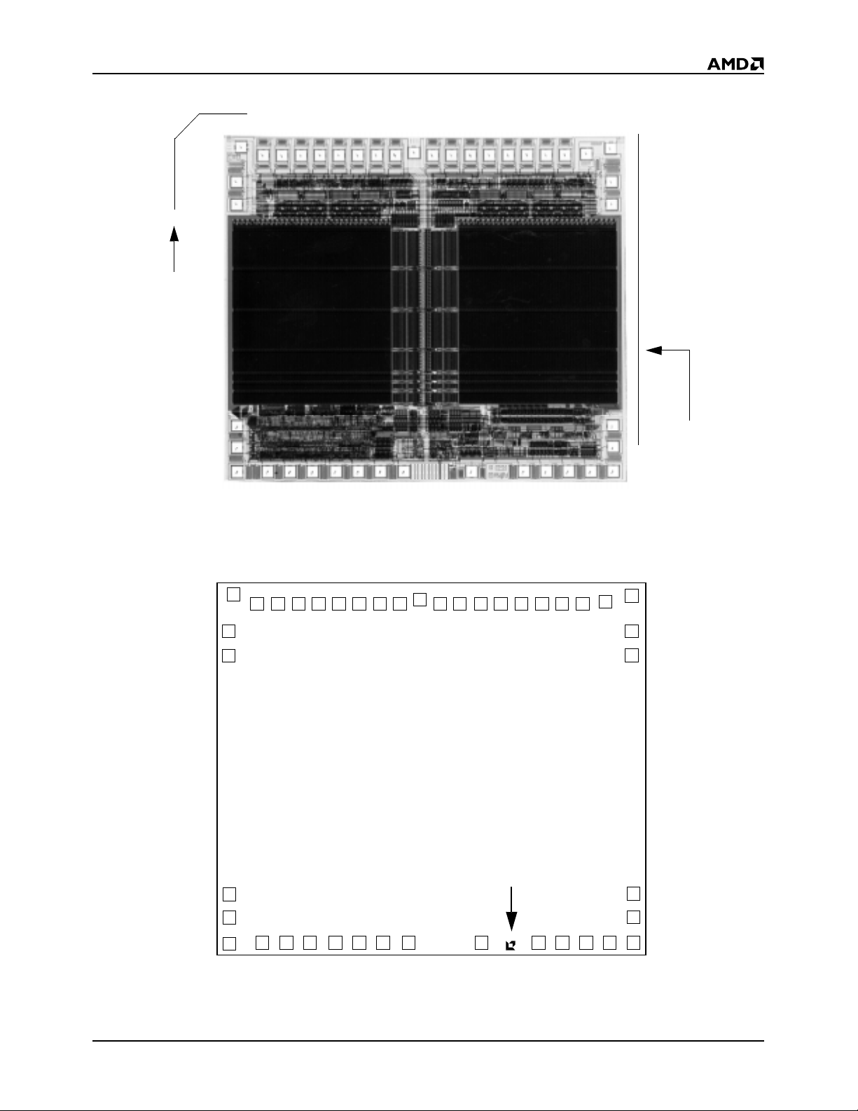
DIE PHOTOGRAPH
Orientation relative
to top left corner of
Gel-Pak
SUPPLEMENT
Orientation relative
to leading edge of
tape and reel
DIE PAD LOCATIONS
10
11
12
13
14
15
42
123456789
AMD logo location
16 17 18 19 20 21 22 23 24 25
3435363738394041
33
32
31
30
29
28
26 27
1/13/98 Am29F200A Known Good Die 3
Page 4

SUPPLEMENT
PAD DESCRIPTION
Pad Signal
1V
CC
2DQ48.5–1.2 –0.2159 –0.0305
3 DQ12 –17.3 –1.2 –0.4394 –0.0305
4 DQ5 –26.1 –1.2 –0.6629 –0.0305
5 DQ13 –34.9 –1.2 –0.8865 –0.0305
6 DQ6 –43.6 –1.2 –1.1074 –0.0305
7 DQ14 –52.4 –1.2 –1.3310 –0.0305
8 DQ7 –61.2 –1.2 –1.5545 –0.0305
9 DQ15/A-1 –69.9 –1.2 –1.7755 –0.0305
10 V
SS
11 BYTE# –82.3 –13.5 –2.0904 –0.3429
12 A16 –82.3 –24.1 –2.0904 –0.6121
13 A15 –82.3 –128.4 –2.0904 –3.2614
14 A14 –82.3 –138.7 –2.0904 –3.5230
15 A13 –82.3 –150.0 –2.0904 –3.8100
16 A12 –68.2 –150.0 –1.7323 –3.8100
17 A11 –57.9 –150.0 –1.4707 –3.8100
18 A10 –47.6 –150.0 –1.2090 –3.8100
19 A9 –36.7 –150.0 –0.9322 –3.8100
20 A8 –26.4 –150.0 –0.6706 –3.8100
21 WE# –16.1 –150.0 –0.4089 –3.8100
22 RESET# –5.2 –150.0 –0.1321 –3.8100
23 RY/BY# 26.1 –150.0 0.6629 –3.8100
24 A7 50.2 –150.0 1.2751 –3.8100
25 A6 60.5 –150.0 1.5367 –3.8100
26 A5 70.8 –150.0 1.7983 –3.8100
27 A4 81.1 –150.0 2.0599 –3.8100
28 A3 91.4 –150.0 2.3216 –3.8100
29 A2 91.5 –138.7 2.3241 –3.5230
30 A1 91.5 –128.4 2.3241 –3.2614
31 A0 91.5 –24.1 2.3241 –0.6121
32 CE# 91.5 –13.6 2.3241 –0.3454
33 V
SS
34 OE# 79.8 –0.7 2.0269 –0.0178
35 DQ0 70.0 –1.2 1.7780 –0.0305
36 DQ8 61.3 –1.2 1.5570 –0.0305
37 DQ1 52.5 –1.2 1.3335 –0.0305
38 DQ9 43.7 –1.2 1.1100 –0.0305
39 DQ2 34.9 –1.2 0.8865 –0.0305
40 DQ10 26.2 –1.2 0.6655 –0.0305
41 DQ3 17.4 –1.2 0.4420 –0.0305
42 DQ11 8.6 –1.2 0.2184 –0.0305
Note: The coordinates above are relative to the center of pad 1 and can be used to operate wire bonding equipment.
Pad Center (mils) Pad Center (millimeters)
XYXY
0.0 0.0 0.0000 0.0000
–80.2 2.7 –2.0371 0.0686
91.1 1.8 2.3139 0.0457
4 Am29F200A Known Good Die 1/13/98
Page 5

SUPPLEMENT
ORDERING INFORMATION
Standard Products
AMD standard products are available in several packages and opera ting ranges. The order number (Valid Combination) is
formed by a combination of the following:
Am29F200A
T
-90
DP
C
1
DIE REVISION
This numbe r ref ers to th e speci fic AMD manuf acturi ng
process and product technology reflected in this
document. It is entered in the revision field of AMD
standard product nomenclature.
TEMPERATURE RANGE
C = Comm ercial (0°C to +70°C)
I=Industrial (–40° C to +85 °C)
E = Extended (–55°C to +125°C)
PACKAGE TYPE AND
MINIMUM ORDER QUANTITY
DP = Waffle Pack
245 die per 5 tray stack
DG = Gel-Pak
486 die per 6 tray stack
DT = Surftape™ (Tape and Reel)
2500 per 7-inch reel
DW = Gel-Pak
Call AMD sales office for minimum order
quantity
SPEED OPTION
See Valid Combinations
®
Die Tray
®
Wafer Tray (sawn wafer on frame)
Am29F200AT-90,
Am29F200AB-90
Am29F200AT-120,
Am29F200AB-120
Valid Combinations
DPC 1, DPI 1, DPE 1,
DGC 1, DGI 1, DGE 1,
DTC 1, DTI 1, DTE 1,
DWC 1, DWI 1, DWE 1
BOOT CODE SECTOR ARCHITECTURE
T = Top sector
B = Bottom sector
DEVICE NUMBER/DESCRIPTION
Am29F200A Known Good Die
2 Megabit (256 K x 8-Bit/128 K x 16-Bit) CMOS Flash Memory—Die Revision 1
5.0 Volt-only Read, Program, and Erase
Valid Combinations
Valid Combinations list configurations planned to be supported in volum e for this device. Co nsult t h e local AMD sales
office to confirm availability of specific valid combinations and
to check on newly released combinations.
1/13/98 Am29F200A Known Good Die 5
Page 6

SUPPLEMENT
PRODUCT TEST FLOW
Figure 1 provides an overview of AMD’s Known Good
Die test flow. For more detailed information, refer to the
Am29F200A product qualification database supplement for KGD. AMD impl ements qual ity assurance procedures throughout the product te st flow. In addition,
Wafer Sort 1
Bake
24 hours at 250°C
Wafer Sort 2
an off-li ne qual ity moni toring program (QMP) f urther
guarantees AMD quality standards are met on Known
Good Die products. These QA procedures also allow
AMD to produce KGD products without requiring or
implementing burn-in.
DC Parameters
Functionality
Programmability
Erasability
Data Retention
DC Parameters
Functionality
Programmability
Erasability
Wafer Sort 3
High Temperature
Packaging for Shipment
Shipment
Figure 1. AMD KGD Product Test Flow
DC Parameters
Functionality
Programmability
Erasability
Speed
Incoming Inspection
Waf er S aw
Die Separation
100% Visual Inspection
Die Pack
6 Am29F200A Known Good Die 1/13/98
Page 7

SUPPLEMENT
PHYSICAL SPECIFICATIONS
Die dimensions . . . . . . . . . . . . . . 191 mils x 174 mils
. . . . . . . . . . . . . . . . . . . . . . . . . . .4.85 mm x 4.42 mm
Die Thickness . . . . . . . . . . . . . . . . . . . . . . . . ~20 mils
Bond Pad Size . . . . . . . . . . . . . . 4.55 mils x 4.55 mils
. . . . . . . . . . . . . . . . . . . . . . . . . . 115.6 µm x 115.6 µm
Pad Area Free of Passivation . . . . . . . . . .20.70 mils
. . . . . . . . . . . . . . . . . . . . . . . . . . . . . . . . . 13,363 µm
Pads Per Die . . . . . . . . . . . . . . . . . . . . . . . . . . . . . .42
Bond Pad Metalization. . . . . . . . . . . . . . . . . . Al/Cu/Si
Die Backside . . . . . . . . . . . . . . . . . . . . . . . . No metal,
may be grounded (optional)
Passivation. . . . . . . . . . . . . . . . . . Nitride/SOG/Nitride
DC OPERATING CONDITIONS
VCC (Supply Voltage). . . . . . . . . . . . . . .4.5 V to 5.5 V
Junction Temperature Under Bias . .T
Operating Temperature
Commercial . . . . . . . . . . . . . . . . . . . 0°C to +70°C
Industrial . . . . . . . . . . . . . . . . . . . –40°C to +85°C
Extended . . . . . . . . . . . . . . . . . . –55°C to +125°C
(max) = 130°C
J
MANUFACTURIN G INFORM ATION
Manufacturing . . . . . . . . . . . . . . . . . . . . . . . . . .FASL
Test . . . . . . . . . . . . . . . . . . . . . . . . . . . . . . . . . . . SDC
Manufacturing ID (Top Boot) . . . . . . . . . . . .98483AK
(Bottom Boot) . . . . . . . .98483ABK
Preparation for Shipment . . . . . . . . Penang, Malaysia
2
Fabrication Process . . . . . . . . . . . . . . . . . . . CS29AF
2
Die Revision . . . . . . . . . . . . . . . . . . . . . . . . . . . . . . . 1
SPECIAL HANDLING INSTR UCTION S
Processing
Do not expose KGD pro ducts to ultraviolet light or
process them at temperature s greater than 250 °C.
Failure to adhere to these handling instructions will
result in irreparable dama ge to the devices. For be st
yield, AMD recommends asse mbly in a Class 10K
clean room with 30% to 60% relative humidity.
Storage
Store at a maximum temperature of 30°C in a nitrogenpurged cabinet or vacuum-sealed bag. Observe all
standard ESD handling procedures.
1/13/98 Am29F200A Known Good Die 7
Page 8

SUPPLEMENT
TERMS AND CONDITIONS OF SALE FOR
AMD NON-VOLATILE MEMORY DIE
All trans actions relati ng to AM D Prod ucts un der th is
agreement shall be subject to AMD’s standard terms
and conditions of sale, or any revisions thereof, which
revisions AMD reserves the right to make at any time
and from time to time. In the event of conflict between
the provisions of AMD’s standard terms and conditions
of sale and this agreement, the terms of this agreement
shall be controlling.
AMD warrants articles of its manufacture against
defective materials or workmanship for a period of
ninety (90) days from date of shipment. This warranty
does no t extend beyond AMD’s cu stomer, and does
not extend to die which has been affixed onto a board
or substrate of any kind. The liability of AMD under this
warranty is limited, at AMD’s option, solely to repair or
to replacement with equivalent articles, or to make an
appropriate credit adj ustment not to exceed the original
sales price, for articles returned to AMD, provided that:
(a) The Buyer promptly notifies AMD in writing of each
and every defect or nonconformity in any article for
which Buyer wishes to make a warranty claim against
AMD; (b) Buyer obtains authorization from AMD to
return the article; (c) the article is returned to AMD,
transportation charges paid by AMD, F .O.B. AMD’s factory; and (d) AMD’s examination of such article discloses to its satisfaction that such alleged defect or
nonconformity actually exists and was not cause d by
negligence, misuse, improper installation, accident or
unauthorized repair or alteration by an entity other than
AMD. The aforementioned provisions do not extend
the original warranty period of any article which has
either been repaired or replaced by AMD.
THIS WARRANT Y IS EXPRE SSED IN LIEU OF ALL
OTHER WARRANTIES, EXPRESSED OR IMPLIED,
INCLUDING THE IMPLIED WARRANTY OF FITNESS
FOR A PARTICULAR PURPOSE, THE IMPLIED
WARRANTY OF MERCHANTABILITY AND OF ALL
OTHER OBLIGATIONS OR LIABILITIES ON AMD’S
PART, AND IT NEITHER ASSUMES NOR AUTH ORIZES ANY OTHER PERSON TO ASSUME FOR
AMD ANY OTHER LIABILITIES. THE FOREGOING
CONSTITUTES THE BUYERS SOLE AND EXCLUSIVE REMEDY FOR THE FURNISHING OF DEFECTIVE OR NON CO NFORM ING ARTICLE S AND AMD
SHALL NOT IN ANY EVENT BE LIABLE FOR
DAMAGES BY REASON OF FAILURE OF ANY
PRODUCT TO FUNCTION PROPERLY OR FOR ANY
SPECIAL, INDIRECT, CO NSEQUENTIAL, INCIDENTAL OR EXEMPLARY DAMAGES, INCLUDING
BUT NO T LIMITED TO , LOSS OF PR OFITS, LO SS
OF USE OR COST OF LABOR BY REASON OF THE
FACT THAT SUCH ARTICLES SHAL L HAVE BEEN
DEFECTIVE OR NON CONFORMING.
Buyer agrees that it will make no warranty representations to its customers which exceed those given by
AMD to Buyer unless and until Buyer shall agree to
indemnify AMD in writing for any claims which exceed
AMD’s warranty. Buyer assumes all respo nsibility for
successful die prep, die attach and wire bonding processes. Due to the unprotected nature of the AMD
Products which are the subject hereof, AMD assumes
no responsibility for environmental effects on die.
AMD products are not designed or authorized for use
as components in life support appliances, d evices or
systems where malfunctio n of a product can reaso nably be expected to result in a personal injury. Buyer’s
use of AMD products for use in life support appli cations
is at Buyer’s own risk and Buyer agrees to fully indemnify AMD for any damages resulting in such use or
sale.
REVISION SUMMARY FOR AM29F2 00A
KNOWN GOOD DIE
Formatted to match current template. Updated Distinctive Characteristics and General Description sections
using the current main data sheet.
Trademarks
Copyright © 1998 Advanced Micro Devices, Inc. All rights reserved.
AMD, the AMD logo, and combinations thereof are registered trademarks of Advanced Micro Devices, Inc.
Product names used in this publication are for identification purposes only and may be trademarks of their respective companies.
8 Am29F200A Known Good Die 1/13/98
 Loading...