

AMD Advanced Micro Devices AM29F100T-120DWI1, AM29F100T-120DWE1, AM29F100T-120DWC1, AM29F100T-120DTI1, AM29F100T-120DTE1 Datasheet
...
SUPPLEMENT
Publication# 21235 Rev: B Amendment/0
Issue Date: January 1998
Am29F100 Known Good Die
1 Megabit (128 K x 8-Bit/64 K x 16-Bit)
CMOS 5.0 Volt-only, Boot Sector Flash Memory—Die Revision 1
DISTINCTIVE CHARACTERISTICS
■ Single power supply operation
—5.0 V ± 10% for read, erase, and program
operations
— Simplifies system-level power requirements
■ High performance
— 120 ns maximum access time
■ Low power consumption
— 20 mA typical active read current for byte mode
— 28 mA typical active read current for word mode
— 30 mA typical program/erase current
— 25 µA typical standby current
■ Flexible sector architecture
— One 16 Kbyte, two 8 Kbyte, one 32 Kbyte, and
one 64 Kbyte sectors (byte mode)
— One 8 Kword, two 4 Kword, one 16 Kword, and
one 32 Kword sectors (word mode)
— Any combination of sectors can be erased
— Supports full chip erase
■ Top or bottom boot block configurations
available
■ Sector protection
— Hardware-based feature that disables/re-
enables program and erase operations in any
combination of sectors
— Sector protection/unprotection can be
implemented using standard PROM
programming equipment
— Temporary Sector Unprotect feature allows in-
system code changes in protected sectors
■ Embedded Algorithms
— Embedded Erase algorithm automatically
pre-programs and erases the chip or any
combination of designated sector
— Embedded Program algorithm automatically
programs and verifies data at specified address
■ Minimum 100,000 program/erase cycles
guaranteed
■ Compatible with JEDEC standards
— Pinout and software compatible with
single-power-supply flash
— Superior inadvertent write protection
■ Data Polling and Toggle Bits
— Provides a software method of detecting
program or erase cycle completion
■ Ready/Busy pin (RY/BY#)
— Provides a hardware method for detecting
program or erase cycle completion
■ Erase Suspend/Erase Resume
— Suspends an erase operation to read data fr om,
or program data to, a sector that is not being
erased, then resumes the erase operation
■ Hardware RESET# pin
— Hardware method of resetting the device to
reading array data
■ T ested to datasheet specifications at
temperature
■ Quality and reliability levels equivalent to
standard packaged components

2 Am29F100 Known Good Die
SUPPLEMENT
GENERAL DESCRIPTION
The Am29F100 in Known Good Die (KGD) form is a 1
Mbit, 5.0 Volt -only Flash memory . AMD defines KGD as
standard product in die form, tested for functionality
and speed. AMD KGD products have the same reliability and quality as AMD products in packaged form.
Am29F100 Features
The Am29F100 is a 1 Mbit, 5.0 V olt-only Flash memory
organized as 131,072 bytes or 65,536 words. Wordwide data appears on DQ0-DQ15; byte-wide data on
DQ0-DQ7. The device is designed to be programmed
in-system with the standard system 5.0 Volt V
CC
sup-
ply. A 12.0 volt V
PP
is not required for program or erase
operations. The device can also be programmed or
erased in standard EPROM programmers.
To eliminate bus contention the device has separate
chip enable (CE#), write ena ble (WE# ) and ou tput enable (OE#) controls.
The device requires only a single 5.0 volt power sup-
ply for both read and write functions. Internally generated and regulated voltages are provided for the
program and erase operations.
The device is entirely command set compatible with the
JEDEC single-power-supply Flash standard. Commands are written to the command register using standard microprocessor write timings. Register contents
serve as input to an internal state machi ne that controls
the erase and programming circuitry. Write cycles also
internally latch addresses and data needed for t he programming and erase operations. Reading data out of
the device is similar to reading from other Flash or
EPROM devices.
Device programming occurs by executing the program
command sequence. This invokes the Embedded
Program algorithm—an internal algorithm that automatically times the program pulse widths and verifies
proper cell margin.
Device erasure occurs by executing the erase command sequence. This invokes the Embedded Erase
algorithm—an internal algorithm that automatically preprograms the array (if it is not already programmed) before executing the erase operation. During erase, the
device automatically times the erase pulse widths and
verifies proper cell margin.
The host system c an detect whether a program or
erase operation is complete by observing the RY/BY#
pin, or by re ading the DQ7 (D ata# Polling) and DQ6
(toggle) status bits. After a program or erase cycle
has been completed, the device is ready to read array
data or accept another command.
The Erase Suspend feature enables the sys tem to put
erase on hold for any period of time to read data from,
or program data to, a sector that is not being erased.
The sec tor erase arc hitecture allows memory sectors
to be erased and reprogrammed without affecting the
data contents of other sectors. The device is erased
when shipped from the factory.
The hardware data protection m easures include a
low V
CC
detector automatically inhibits write operat ions
during power transitions. The hardware sector pro-
tection feature disables both program and erase operations in any combination of the sectors of memory,
and is implemented using standard EPROM programmers. The temporary sector unprotect feature allows
in-system changes to protected sectors.
The hardware RESET# pin terminates any operation
in progress and resets the internal state machine to
reading array data. The RESET# pin may be tied to the
system reset circuitry. A system reset would thus also
reset the device, enabling the system microprocessor
to read the boot-up firmware from the Flash memory.
The system can place the device into the standby mode.
Power consumption is greatly reduced in t his mode.
AMD’s Flash technology combines years of Flash
memory manufacturing experience to produce the
highest levels of quality, reliability, and cost
effectiveness. The device electrically erases all bits
within a sector simultaneously via Fowler-Nordheim
tunneling. The bytes are programmed one byte at a
time using the EPROM programming mechanism of
hot electron injection.
ELECTRICAL SPECIFICATIONS
Refer to the Am29F100 data sheet, document number
18926, for full electrical specifications on the
Am29F100.
Am29F100 Known Good Die 3
SUPPLEMENT
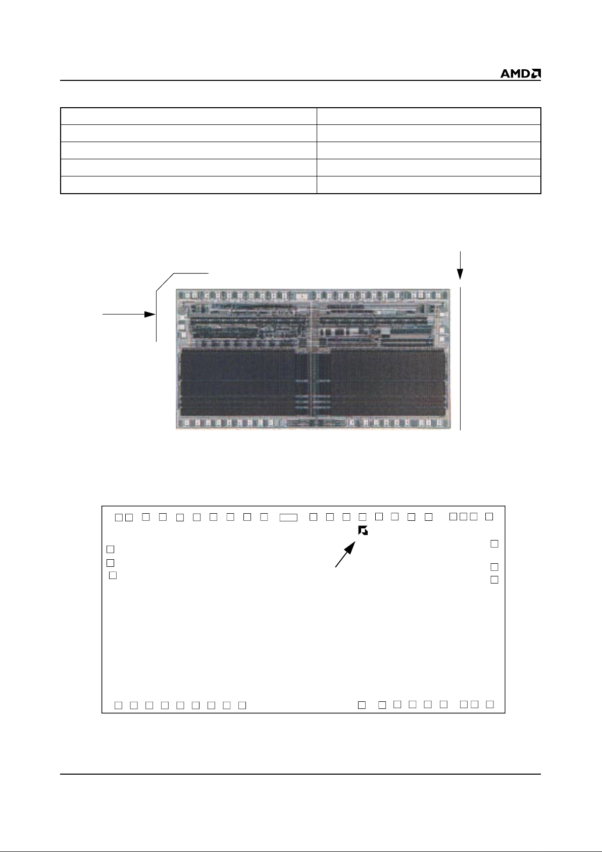
PRODUCT SELECTOR GUIDE
DIE PHOTOGRAPH
DIE PAD LOCATIONS
Family Part Number Am29F100 KGD
Speed Option (V
CC
= 5.0 V ± 10%) -120
Max Access Time, t
ACC
(ns) 120
Max CE# Access, t
CE
(ns) 120
Max OE# Access, t
OE
(ns) 50
Orientation relative
to top left corner of
Gel-Pak
Orientation relative
to leading edge of
tape and reel
1234567891011
12
13
14
15 16 17 18 19 20 21 22 23 24 25 26 27 28 29 30
AMD logo locati on
31 32
33
34
35
363738394041424344454647
4 Am29F100 Known Good Die
SUPPLEMENT
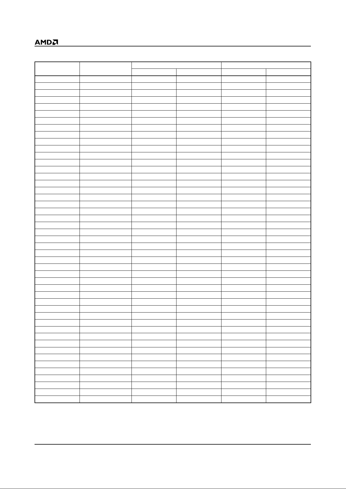
PAD DESCRIPTION
Note: The coordinates above are relative to the center of pad 1 and can be used to operate wire bonding equipment.
Pad Signal
Pad Center (mils) Pad Center (millimeters)
XYXY
1V
CC
0.0 0.0 0.00 0.00
2DQ4–16.5 0.6 –0.42 0.02
3 DQ12 –27.0 0.6 –0.69 0.02
4 DQ5 –37.8 0.6 –0.96 0.02
5 DQ13 –48.4 0.6 –1.23 0.02
6 DQ6 –59.1 0.6 –1.50 0.02
7 DQ14 –69.7 0.6 –1.77 0.02
8 NC –80.5 0.6 –2.04 0.02
9 DQ7 –91.0 0.6 –2.31 0.02
10 NC –103 0.6 –2.62 0.02
11 NC –109.6 0.6 –2.78 0.02
12 DQ15 –114.7 –20.6 –2.91 –0.52
13 V
SS
–114.7 –29.5 –2.91 –0.75
14 BYTE# –113.3 –37.0 –2.88 –0.94
15 A15 –110.2 –121.9 –2.80 –3.10
16 A14 –100.0 –121.9 –2.54 –3.10
17 A13 –90.0 –121.9 –2.29 –3.10
18 A12 –79.9 –121.9 –2.03 –3.10
19 A11 –69.9 –121.9 –1.78 –3.10
20 A10 –59.9 –121.9 –1.52 –3.10
21 A9 –49.9 –121.9 –1.27 –3.10
22 A8 –39.9 –121.9 –1.01 –3.10
23 WE# –29.9 –121.9 –0.76 –3.10
24 RESET# 47.8 –121.9 1.21 –3.10
25 RY/BY# 61.2 –121.9 1.55 –3.10
26 A7 71.1 –121.9 1.81 –3.10
27 A6 81.1 –121.9 2.06 –3.10
28 A5 91.0 –121.9 2.31 –3.10
29 A4 101.1 –121.9 2.57 –3.10
30 A3 114.5 –121.9 2.91 –3.10
31 A2 121.4 –121.9 3.08 –3.10
32 A1 131.4 –121.9 3.34 –3.10
33 A0 134.5 –41.1 3.42 –1.04
34 CE# 134.5 –32.7 3.42 –0.83
35 V
SS
134.5 –17.6 3.42 –0.45
36 OE# 130.7 0.6 3.32 0.02
37 NC 120.9 0.6 3.07 0.02
38 NC 114.2 0.6 2.90 0.02
39 NC 107.5 0.6 2.73 0.02
40 DQ0 91.6 0.6 2.33 0.02
41 DQ8 80.2 0.6 2.04 0.02
42 DQ1 69.4 0.6 1.76 0.02
43 DQ9 58.9 0.6 1.50 0.02
44 DQ2 48.1 0.6 1.22 0.02
45 DQ10 37.5 0.6 0.95 0.02
46 DQ3 26.7 0.6 0.68 0.02
47 DQ11 16.2 0.6 0.41 0.02

Am29F100 Known Good Die 5
SUPPLEMENT
ORDERING INFORMATION
Standard Pr od ucts
AMD standard products are available in several packages and operating ranges. The order number (Valid Combination) is
formed by a combination of the following:
Valid Combinations
Valid Combinations list configurations planned to be supported in volume for this device. Consult the local AMD sales
office to confirm availability of specific valid combinations and
to check on newly released combinations.
Am29F100
DEVICE NUMBER/DESCRIPTION
Am29F100 Known Good Die
1 Megabit (128 K x 8-Bit/64K x 16-Bit) CMOS Flash Memory—Die Revision 1
5.0 Volt-only Program and Erase
-120
DP
C
1
DIE REVISION
This number refers to the specific AMD manufacturing
process and product technology reflected in this
document. It is entered in the revision field of AMD
standard product nomenclature.
TEMPERATURE RANGE
C = Commercial (0°C to +70°C)
I = Industrial (–40°C to +85°C)
E = Extended (–55°C to +125°C)
PACKAGE TYPE AND
MINIMUM ORDER QUANTITY
DP = Waffle Pack
180 die per 5 tray stack
DG = Gel-Pak
®
Die Tray
420 die per 6 tray stack
DT = Surft ape ™ (Ta pe and Reel)
1600 per 7-inch reel
DW = Gel-Pak
®
Wafer Tray (sawn wafer on frame)
Call AMD sales office for minimum order
quantity
SPEED OPTION
See Valid Combinations
BOOT CODE SECTOR ARCHITECTURE
T = Top sector
B = Bottom sector
T
Valid Combinations
Am29F100T-120
Am29F100B-120
DPC 1, DPI 1, DPE 1,
DGC 1, DGI 1, DGE 1,
DTC 1, DTI 1, DTE 1,
DWC 1, DWI 1, DWE 1

6 Am29F100 Known Good Die
SUPPLEMENT
PRODUCT TEST FLOW
Figure 1 provides an overview of AMD’s Known Good
Die test flow. For more detailed infor mation, refer to the
Am29F100 product qualification database supplement
for KGD. AMD implements quality assurance procedures throughout the product test flow. In addition, an
off-line quality monitoring program (QMP) further guarantees AMD quality standards are met on Known Good
Die products. These QA procedures also allow AMD to
produce KGD products without requiring or implementing burn-in.
Figure 1. AMD KGD Product Test Flow
Wafer Sort 1
Bake
24 hours at 250°C
Wafer Sort 2
Wafer Sort 3
High Temperature
Packaging for Shipment
Shipment
DC Parameters
Functionality
Programmability
Erasability
Data Retention
DC Parameters
Functionality
Programmability
Erasability
DC Parameters
Functionality
Programmability
Erasability
Speed
Incoming Inspection
Wafer Saw
Die Separation
100% Visual Inspection
Die Pack

Am29F100 Known Good Die 7
SUPPLEMENT
PHYSICAL SPECIFICATIONS
Die dimensions . . . . . . . . . . . . . . 266 mils x 142 mils
. . . . . . . . . . . . . . . . . . . . . . . . . . .6.76 mm x 3.61 mm
Die Thickness . . . . . . . . . . . . . ~20 mils or ~0.51 mm
Bond Pad Size. . . . . . . . . . . . . . 4.64 mils x 4.64 mils
. . . . . . . . . . . . . . . . . . . . . . . . . . 117.8 µm x 117.8 µm
Pad Area Free of Passivation . . . . . . . . . .21.53 mils
2
. . . . . . . . . . . . . . . . . . . . . . . . . . . . . . . . . 13,877 µm
2
Pads Per Die . . . . . . . . . . . . . . . . . . . . . . . . . . . . . .47
Bond Pad Metalization. . . . . . . . . . . . . . . . . . Al/Si/Cu
Die Backside . . . . . . . . . . . . . . . . . . . . . . . . No metal,
may be grounded (optional)
Passivation. . . . . . . . . . . . . . . . . . Nitride/SOG/Nitride
DC OPERATING CONDITIONS
VCC (Supply Volt age). . . . . . . . . . . . . . .4.5 V to 5.5 V
Junction Temperature Under Bias . .T
J
(max) = 130°C
Operating Temperature
. . . . . . . . . . . . . . . . . . . . . . Commercial 0°C to +70°C
Industrial . . . . . . . . . . . . . . . . . . . –40°C to +85°C
Extended . . . . . . . . . . . . . . . . . . –55°C to +125°C
MANUFACTURING INFORMATION
Manufacturing and Test. . . . . . . . . Fab 14, Austin, TX
Manufacturing ID (Top Boo t) . . . . . . . . . . . . 98242AK
(Bottom Boot) . . . . . . . .98242ABK
Preparation for Shipment . . . . . . . . Penang, Malaysia
Fabrication Process . . . . . . . . . . . . . . . . . CS19AFDS
Die Revision . . . . . . . . . . . . . . . . . . . . . . . . . . . . . . . 1
SPECIAL HANDLING INSTRUCTIONS
Processing
Do not expose KGD products to ultraviolet light or
process them at temperatures greater than 250°C.
Failure to adhe re to these handling instructions will
result in irrep arable damage to the devices. For best
yield, AMD recommends assembly in a Class 10K
clean room with 30% to 60% relative humidity.
Storage
Store at a maximum temperature of 30°C in a nit rogenpurged cabinet or vacuum-sealed bag. Observe all
standard ESD handling procedures.

8 Am29F100 Known Good Die
SUPPLEMENT
TERMS AND CONDITIONS OF SALE FOR
AMD NON-VOLATILE MEMORY DIE
All transactions relating to AMD Products under this
agreement shall be subj ect to AMD’s standard terms
and conditions of sale, or any revisions thereof, which
revisions AMD reserves the right to make at any time
and from time to time. In the event of conflict between
the provisions of AMD’s standard terms and conditions
of sale and this agreement, the terms of this agreement
shall be controlling.
AMD warrants ar ticles of its manufacture against
defective materials or workmanship for a period of
ninety (90) days from date of shipment. This warranty
does not extend beyond AMD’s customer, and does
not extend to die which has been affixed onto a board
or substrate of any kind. Th e liabil ity of AMD und er t his
warranty is limited, at AMD’s option, solely to repair or
to replacement with equivalent articles, or to make an
appropriate credit adjustment not to exceed th e original
sales price, for articles returned to AMD, provided that:
(a) The Buyer promptly notifies AMD in writing of each
and every defect or nonconformity in any article for
which Buyer wishes to make a warranty claim against
AMD; (b) Buyer obtains authorization from AMD to
return the article; (c) the article is returned to AMD,
transportation charges paid by AMD, F . O.B. AMD’s factory; and (d) AMD’s examination of such article discloses to its satisfaction that such alleged defect o r
nonconformity actually exists and was not caused by
negligence, misuse, improper installation, accident or
unauthorized repair or alteration by an entity othe r than
AMD. The aforementioned provisions do not extend
the original warranty period of any article which has
either been repaired or replaced by AMD.
THIS WARRANTY IS EXPRESSED IN LIEU OF AL L
OTHER WARRANTIES, EXPRESSED OR IMPLIED,
INCLUDING THE IMPLIED W ARRANTY OF FITNESS
FOR A PARTICULAR PURPOSE, THE IMPLIED
WARRANTY OF MERCHANTABILITY AND OF ALL
OTHER OBLIGATIONS OR LIABILITIES ON AMD’S
PART, AND IT NEITHER ASSUMES NOR AUTHORIZES ANY OTHER PERSON TO ASSUME FOR
AMD ANY OTHER LIABILITIES. THE FOREGOING
CONSTITUTES THE BUYERS SOLE AND EXCLUSIVE REMEDY FOR THE FURNISHING OF DEFECTIVE OR NON CONFORMING ARTICLES AND AMD
SHALL NOT IN ANY EVENT BE LIABLE FOR
DAMAGES BY REASON OF FAILURE OF ANY
PRODUCT TO FUNCTION PROPERL Y OR FOR ANY
SPECIAL, INDIRECT, CONSEQUENTIAL, INCIDENTAL OR EXEMPLARY DAMAGES, INCLUDING
BUT NOT LIMITED TO, LOSS OF PROFITS, LOSS
OF USE OR COST OF LABOR BY REASON OF THE
FACT THAT SUCH ARTICLES SHALL HAVE BEEN
DEFECTIVE OR NON CONFORMING.
Buyer agrees that it will make no warranty representations to its customers which exceed those given by
AMD to Buyer unless and until Buyer s hall agree to
indemnify AMD in writing for any claims which exceed
AMD’s warranty. Buyer assumes all responsibility for
successful die prep, die attach and wire bonding processes. Due to the unprotected nature of the AMD
Products which are the subject hereof, AMD assumes
no responsibility for environmental effects on die.
AMD products are not designed or authorized for use
as componen ts in life suppor t appliances, d evices or
systems where malfunction of a product can reasonably be expected to result in a personal injury. Buyer’s
use of AMD products for use in life support applications
is at Buyer’s own risk and Buyer agrees to fully indemnify AMD for any damages resulting in s uch use or
sale.
REVISION SUMMARY FOR AM29F100
KNOWN GOOD DIE
Formatted to match current template. Updated Dist inctive Characteristics and General Descriptio n sections
using the current main data sheet. Changed Surftape
quantity to 1600.
Trademarks
Copyright © 1998 Advanced Micro Devices, Inc. All rights reserved.
AMD, the AMD logo, and combinations thereof are registered trademarks of Advanced Micro Devices, Inc.
Product names used in this publication are for identification purposes only and may be trademarks of their respective companies.
 Loading...