

Datasheet AM29F040-120EC, AM29F040-120PI, AM29F040-120PE, AM29F040-120PCB, AM29F040-120PC Datasheet (AMD Advanced Micro Devices)
...Page 1

FINAL
Am29F040
4 Megabit (524,288 x 8-Bit) CMOS 5.0 Volt-only,
Sector Erase Flash Memory
DISTINCTIVE CHARACTERISTICS
■
5.0 V ± 10% for read and write operations
— Minimizes system level power requirements
■
Compatible with JEDEC-standards
— Pinout and software compatible with single-
power-supply Flash
— Superior inadvertent write protection
■
Package options
— 32-pin PLCC
— 32-pin TSOP
— 32-pin PDIP
■
Minimum 100,000 write/erase cycles guaranteed
■
High performance
— 55 ns maximum access time
■
Sector erase architecture
— Uniform sectors of 64 Kbytes each
— Any combination of sectors can be erased.
Also supports full chip erase.
■
Sector protection
— Hardware method that disables any combination
of sectors from write or erase operations
■
Embedded Erase Algorithms
— Automatically preprograms and erases the chip
or any combination of sectors
■
Embedded Program Algorithms
— Automatically programs and verifies data at
specified address
■
Data
Polling and T oggle Bit f eature for detection
of program or erase cycle completion
■
Erase suspend/resume
— Supports reading data from a sector not being
erased
■
Low power consumption
— 20 mA typical active read current
— 30 mA typical program/erase current
■
Enhanced power management for standby
mode
— <1 µA typical standby current
— Standard access time from standby mode
GENERAL DESCRIPTION
The Am29F040 is a 4 Mbit, 5.0 Volt-only Flash memory
organized as 512 Kbytes of 8 bits each. The Am29F040
is offered in a 32-pin package. This device is designed
to be programmed in-system with the standard system
5.0 V VCC supply. A 12.0 V VPP is not required for
write or erase operations. The device can also be
reprogrammed in standard EPROM programmers .
The standard Am29F040 offers access times between
55 ns and 150 ns, allowing operation of high-speed
microprocessors without wait states. To eliminate bus
contention the device has separate chip enable (CE
write enable (WE
The Am29F040 is entirely command set compatible
with the JEDEC single-power-supply Flash standard.
Commands are written to the command register using
standard microprocessor write timings. Register contents serve as input to an internal state machine
) and output enable (OE) controls.
which controls the erase and programming circuitry.
Write cycles also internally latch addresses and data
needed for the programming and erase operations.
Reading data out of the device is similar to reading
from 12.0 Volt Flash or EPROM devices.
The Am29F040 is programmed by executing the program command sequence. This will inv oke the Embedded Program Algorithm which is an internal algorithm
that automatically times the program pulse widths and
verifies proper cell margin. Typically, each sector can
be programmed and verified in less than one second.
),
Erase is accomplished by executing the erase command sequence. This will invoke the Embedded Erase
Algorithm which is an internal algorithm that automatically preprograms the array if it is not already programmed before e x ecuting the er ase operation. During
erase, the device automatically times the erase pulse
widths and verifies proper cell margin.
Publication# 17113 Rev: E Amendment/0
Issue Date: November 1996
Page 2
Any individual sector is typically erased and verified in
1.0 seconds (if already completely preprogrammed).
This device also features a sector erase architecture.
The sector mode allows for 64K byte b loc ks of memory
to be erased and reprogrammed without affecting
other blocks. The Am29F040 is erased when shipped
from the factory.
The device features single 5.0 V power supply operation for both read and write functions. Internally generated and regulated voltages are provided for the
program and erase operations. A low VCC detector
automatically inhibits write operations on the loss of
power . The end of progr am or erase is detected by Data
Polling of DQ7 or by the Toggle Bit feature on DQ6.
Once the end of a program or erase cycle has been
completed, the device internally resets to the read
mode.
AMD’s Flash technology combines years of EPROM
2
and E
PROM experience to produce the highest lev els
of quality, reliability and cost effectiveness. The
Am29F040 memory electrically erases the entire chip
or all bits within a sector simultaneously via FowlerNordheim tunneling. The bytes are programmed one
byte at a time using the EPROM programming
mechanism of hot electron injection.
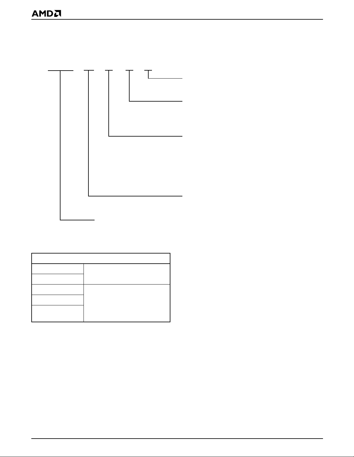
Flexible Sector-Erase Architecture
■
Eight 64 Kbyte sectors
■
Individual-sector, multiple-sector, or bulk-erase
capability
■
Individual or multiple-sector protection is user
definable
7FFFFh
6FFFFh
64 Kbytes per Sector
5FFFFh
4FFFFh
3FFFFh
2FFFFh
1FFFFh
0FFFFh
00000h
17113E-1
2 Am29F040
Page 3
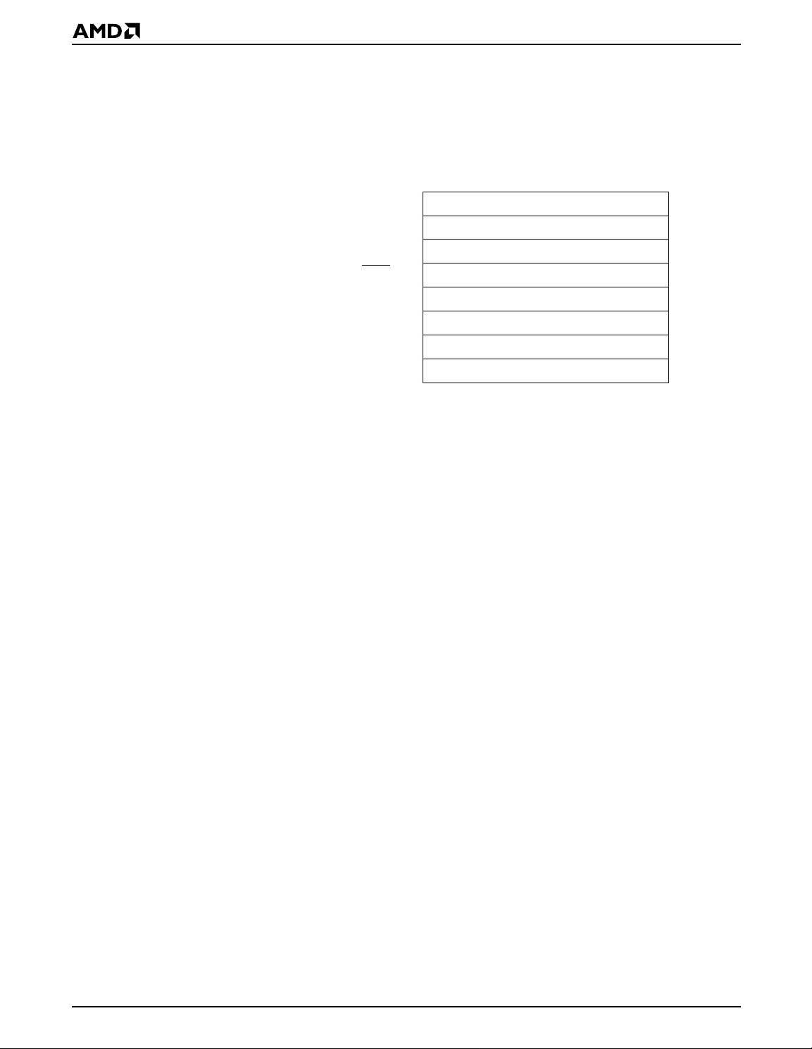
PRODUCT SELECTOR GUIDE
Family Part No: Am29F040
Ordering Part No: VCC = 5.0 V ± 5%
VCC = 5.0 V ± 10%
Max Access Time (ns) 55 70 90 120 150
(E) Access (ns) 55 70 90 120 150
CE
OE (G) Access (ns) 25 30 35 50 55
-55
-70 -90 -120 -150
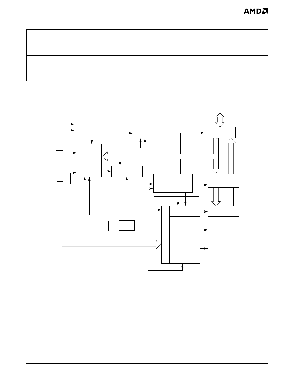
BLOCK DIAGRAM
DQ0–DQ7
V
CC
V
SS
Erase V oltage
Generator
Input/Output
Buffers
A0–A18
WE
CE
OE
State
Control
Command
Register
V
Detector
CC
PGM V oltage
Generator
Timer
Chip Enable
Output Enable
STB
Logic
Y-Decoder
Address Latch
STB
Data Latch
Y-Gating
Cell MatrixX-Decoder
17113E-2
Am29F040 3
Page 4
CONNECTION DIAGRAMS
PDIP PLCC
A18
A16
A15
A12
DQ0
DQ1
DQ2
V
A11
A9
A8
A13
A14
A17
WE
V
CC
A18
A16
A15
A12
A7
A6
A5
A4
A7
A6
A5
A4
A3
A2
A1
A0
SS
32
31
30
29
28
27
26
25
24
23
22
21
20
19
18
17
V
CC
WE
A17
A14
A13
A8
A9
A11
OE
A10
CE
DQ7
DQ6
DQ5
DQ4
DQ3
17113E-3
A7
A6
A5
A4
A3
A2
A1
A0
DQ0
5
6
7
8
9
10
11
12
13
A12
DQ1
A15
A16
A18
1313023432
17 18 19 20161514
SS
V
DQ2
DQ3
CC
V
DQ4
WE
DQ5
A17
29
28
27
26
25
24
23
22
21
DQ6
A14
A13
A8
A9
A11
OE
A10
CE
DQ7
17113E-4
1
2
3
4
5
6
7
8
9
10
11
12
13
14
15
16
TSOP
1
2
3
4
5
6
7
8
9
10
11
12
13
14
15
16
32
31
30
29
28
27
26
25
24
23
22
21
20
19
18
17
OE
A10
CE
DQ7
DQ6
DQ5
DQ4
DQ3
V
SS
DQ2
DQ1
DQ0
A0
A1
A2
A3
29F040 Standard Pinout
OE
A10
CE
DQ7
DQ6
DQ5
DQ4
DQ3
V
SS
DQ2
DQ1
DQ0
A0
A1
A2
A3
1
2
3
4
5
6
7
8
9
10
11
12
13
14
15
16
29F040 Reverse Pinout
4 Am29F040
32
31
30
29
28
27
26
25
24
23
22
21
20
19
18
17
A11
A9
A8
A13
A14
A17
WE
V
CC
A18
A16
A15
A12
A7
A6
A5
A4
17113E-5
Page 5
PIN CONFIGURATION
A0–A18 = Address Inputs
DQ0–DQ7 = Data Input/Output
CE
OE = Output Enable
WE = Write Enable
V
SS
V
CC
= Chip Enable
= Device Ground
= Device Power Supply
(5.0 V ±10% or ±5%)
LOGIC SYMBOL
19
A0–A18
CE
(E)
(G)
OE
WE
(W)
8
DQ0–DQ7
17113E-6
Am29F040 5
Page 6
ORDERING INFORMATION
Standard Products
AMD standard products are available in se v eral packages and oper ating ranges. The order number (Valid Combination) is formed
by a combination of:
AM29F040 -55 E C
DEVICE NUMBER/DESCRIPTION
Am29F040
4 Megabit (524,288 x 8-Bit) CMOS 5.0 Volt-only, Sector Erase Flash Memory
B
OPTIONAL PROCESSING
Blank = Standard Processing
B = Burn-In
TEMPERATURE RANGE
C = Commercial (0
I = Industrial (–40
E = Extended (–55
P ACKA GE TYPE
P = 32-Pin Plastic DIP (PD 032)
J = 32-Pin Rectangular Plastic Leaded Chip
Carrier (PL 032)
E = 32-Pin Thin Small Outline Package (TSOP)
Standard Pinout (TS 032)
F = 32-Pin Thin Small Outline Package (TSOP)
Reverse Pinout (TSR032)
SPEED OPTION
See Product Selector Guide
and Valid Combinations
°C to +70°C)
°C to +85°C)
°C to +125°C)
Valid Combinations
AM29F040-55
AM29F040-70
AM29F040-90 PC, PCB, PI, PIB, PE, PEB,
AM29F040-120
AM29F040-150
JC, JI, JE, EC, EI, EE, FC, FI, FE
JC, JCB, JI, JIB, JE, JEB,
EC, ECB, EI, EIB, EE, EEB,
FC, FCB, FI, FIB, P11
FE, FEB
Valid Combinations
Valid Combinations list configurations planned to be supported in volume for this device. Consult the local AMD sales
office to confirm availability of specific valid combinations and
to check on newly released combinations.
6 Am29F040
Page 7
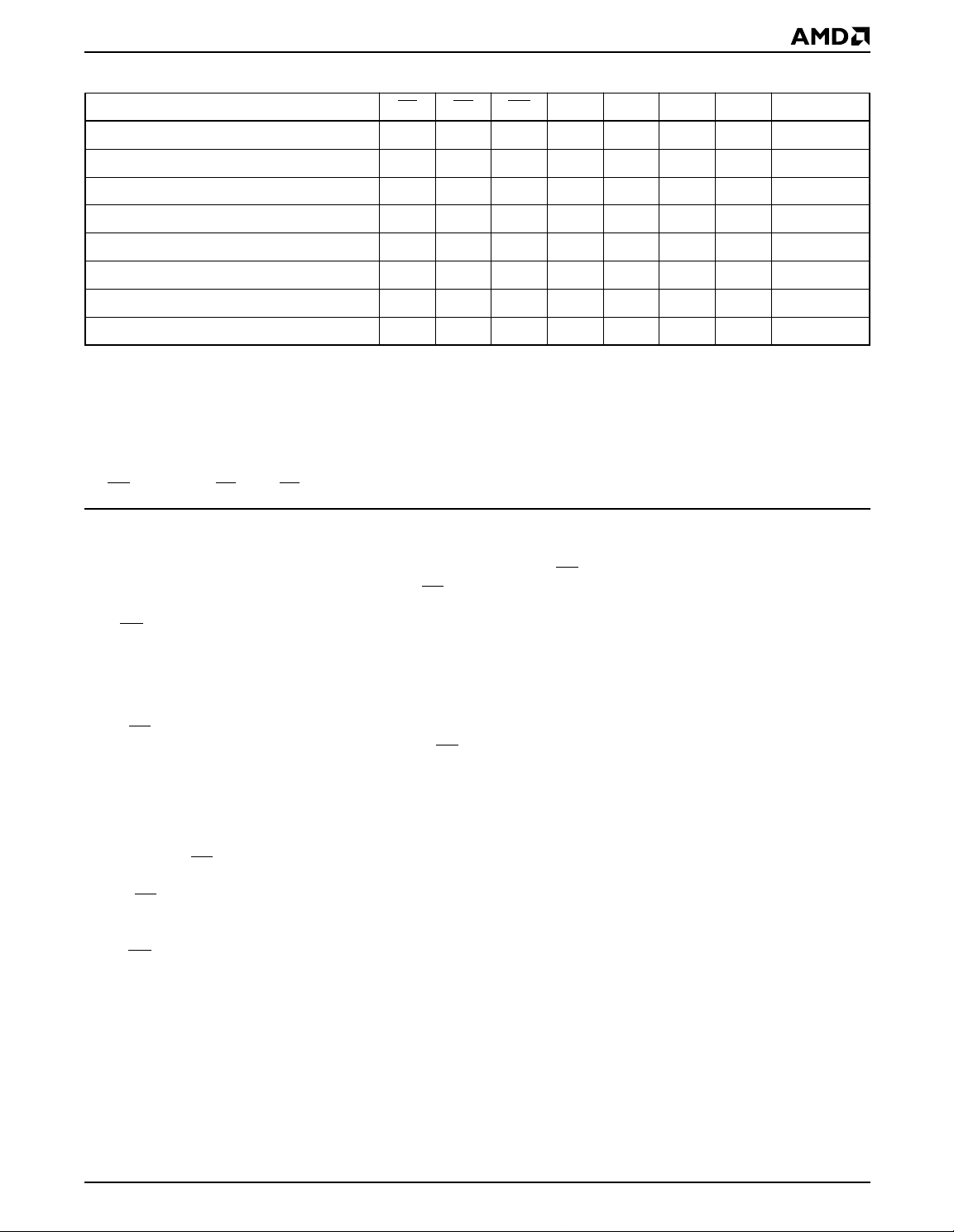
Table 1. Am29F040 User Bus Operations
Operation CE
Autoselect Manufacturer Code (Note 1) L L H L L L V
Autoselect Device Code (Note 1) L L H H L L V
Read (Note 4) L L H A0 A1 A6 A9 RD
Standby H XXXXXXHIGH Z
Output Disable L H H XXXXHIGH Z
Write L H L A0 A1 A6 A9 PD (Note 2)
Verify Sector Protect (Note 3) L LHLHLVIDCode
Autoselect Device Unprotect Code L L H H H L V
Legend:
L = Logic 0, H = Logic 1, X = Don’t Care. See DC Characteristics for voltage levels.
Notes:
1. Manufacturer and device codes may also be accessed via a command register write sequence. Refer to Tables 2 and 4.
2. Refer to Table 3 for valid PD (Program Data) during a write operation.
3. Refer to the section on Sector Protection.
4. WE can be VIL if OE is VIL, OE at VIH initiates the write operations.
Read Mode
The Am29F040 has two control functions which must
be satisfied in order to obtain data at the outputs. CE
the power control and should be used for de vice selection. OE is the output control and should be used to
gate data to the output pins if a device is selected.
Address access time (t
) is equal to the delay from
ACC
stable addresses to valid output data. The chip enable
access time (tCE) is the delay from stable addresses and
stable CE
to valid data at the output pins. The output enable access time is the delay from the f alling edge of OE
to valid data at the output pins (assuming the addresses
have been stable for at least t
ACC–tOE
time).
Standby Mode
The Am29F040 has two standby modes, a CMOS
standby mode (CE
input held at V
current consumed is less than 5 µA; and a TTL standb y
mode (CE
is held at V
) when the current required is
IH
reduced to approximately 1 mA. In the standby mode
the outputs are in a high impedance state, independent
of the OE
input.
If the device is deselected during erasure or programming, the device will draw active current until the
operation is completed.
± 0.5 V), when the
CC
OE WE A0 A1 A6 A9 I/O
ID
ID
ID
Output Disable
is
With the OE
input at a logic high level (V
the device is disabled. This will cause the output pins to
be in a high impedance state.
), output from
IH
Autoselect
The autoselect mode allows the reading out of a binary
code from the device and will identify its manufacturer
and type. This mode is intended for use b y programming
equipment for the purpose of automatically matching the
device to be programmed with its corresponding programming algorithm. This mode is functional over the
entire temperature range of the device.
To activate this mode, the programming equipment
must force VID
Two identifier bytes may then be sequenced from the
device outputs by toggling address A0 from VIL to VIH.
All addresses are don’t cares except A0, A1, and A6.
The manufacturer and device codes may also be read
via the command register, for instances when the
Am29F040 is erased or programmed in a system without access to high voltage on the A9 pin. The command
sequence is illustrated in Table 4 (refer to Autoselect
Command section).
Byte 0 (A0 = VIL) represents the manufacturer’s code
(11.5 V to 12.5 V) on address pin A9.
Code
Code
Code
(AMD = 01H) and byte 1 (A0 = VIH) the device identifier
code (Am29F040 = A4H). All identifiers for manufacturer and device exhibit odd parity with the MSB (DQ7)
defined as the parity bit. See Table 2.
Am29F040 7
Page 8
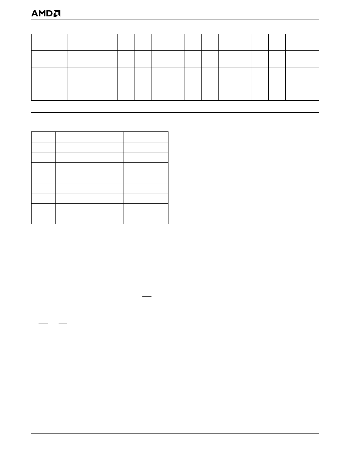
Table 2. Am29F040 Autoselect Codes
Type A18 A17 A16 A6 A1 A0
Manufacturer
ID
Am29F040
Device ID
Sector Protection
*Outputs 01H at protected sector addresses
XXXVILV
XXXV
Sector Addresses V
IL
IL
Code
(HEX) DQ7 DQ6 DQ5 DQ4 DQ3 DQ2 DQ1 DQ0
VIL01H00000001
IL
V
VIHA4H10100100
IL
V
VIL01H* 00000001
IH
Table 3. Sector Addresses
A18 A17 A16 Address Range
SA0 0 0 0 00000h–0FFFFh
SA1 0 0 1 10000h–1FFFFh
SA2 0 1 0 20000h–2FFFFh
SA3 0 1 1 30000h–3FFFFh
SA4 1 0 0 40000h–4FFFFh
SA5 1 0 1 50000h–5FFFFh
SA6 1 1 0 60000h–6FFFFh
SA7 1 1 1 70000h–7FFFFh
Write
Device erasure and programming are accomplished
via the command register. The contents of the register
serve as inputs to the internal state machine. The state
machine outputs dictate the function of the device.
The command register itself does not occupy any
addressable memory location. The register is a latch
used to store the commands, along with the address
and data information needed to execute the command.
The command register is written by bringing WE
while CE
is at V
latched on the falling edge of WE
and OE
IL
is at V
. Addresses are
IH
or CE, whichever
happens later; while data is latched on the rising edge
of WE or CE, whichever happens first. Standard
microprocessor write timings are used.
Refer to AC Write Characteristics and the Erase/
Programming W av eforms for specific timing par ameters.
to V
IL
Sector Protection
The Am29F040 features hardware sector protection.
This feature will disable both program and erase
operations in any number of sectors (0 through 8). The
sector protect feature is enabled using programming
equipment at the user’s site. The device is shipped with
all sectors unprotected. Alternatively, AMD may program and protect sectors in the factory prior to shipping
the device (AMD’s ExpressFlash™ Service).
It is also possible to determine if a sector is protected
in the system by writing an Autoselect command.
Performing a read operation at the address location
XX02H, where the higher order addresses (A16,
A17, and A18) are used to select the desired sector.
The device produces a logical “1” at DQ0 for a protected sector and a logical “0” for an unprotected
sector. See Table 2 for Autoselect codes.
Sector Unprotect
The Am29F040 also features a sector unprotect mode
so that a protected sector may be unprotected to
incorporate any changes in the code. The sector unprotect is enabled using programming equipment at the
user’s site.
,
Command Definitions
Device operations are selected by writing specific address and data sequences into the command register.
Writing incorrect address and data values or writing
them in the improper sequence will reset the device to
read mode. Table 4 defines the valid register command
sequences. Note that the Erase Suspend (B0) and
Erase Resume (30) commands are valid only while the
Sector Erase operation is in progress. Either of the two
reset commands will reset the device (when applicable).
8 Am29F040
Page 9
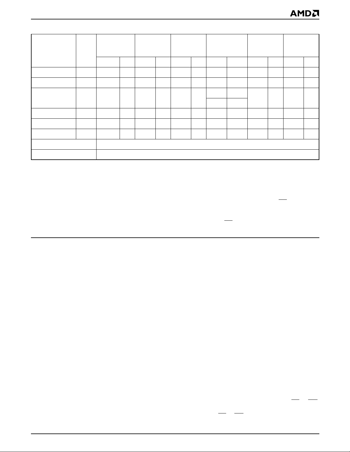
Table 4. Am29F040 Command Definitions
Bus
Command
Sequence
Read/Reset
Read/Reset 1 XXXXH F0H
Read/Reset 4 5555H AAH 2AAAH 55H 5555H F0H RA RD
Autoselect 4 5555H AAH 2AAAH 55H 5555H 90H
Byte Program 4 5555H AAH 2AAAH 55H 5555H A0H PA PD
Chip Erase 6 5555H AAH 2AAAH 55H 5555H 80H 5555H AAH 2AAAH 55H 5555H 10H
Sector Erase 6 5555H AAH 2AAAH 55H 5555H 80H 5555H AAH 2AAAH 55H SA 30H
Sector Erase Suspend Erase can be suspended during sector erase with Addr (don’t care), Data (B0H)
Sector Erase Resume Erase can be resumed after suspend with Addr (don’t care), Data (30H)
Notes:
1. Address bits A15, A16, A17, and A18 = X = Don’t Care for all address commands except for Program Address (PA), Sector
Address (SA), Read Address (RA), and autoselect sector protect verify.
2. Bus operations are defined in Table 1.
3. RA = Address of the memory location to be read.
PA = Address of the memory location to be programmed. Addresses are latched on the falling edge of the WE pulse.
SA = Address of the sector to be erased. The combination of A18, A17, A16 will uniquely select any sector (see Table 3).
4. RD = Data read from location RA during read operation.
PD = Data to be programmed at location PA. Data is latched on the rising edge of WE
5. Read from non-erasing sectors is allowed in the Erase Suspend mode.
Write
Cycles
Req’ d
First Bus
Write Cycle
Addr Data Addr Data Addr Data Addr Data Addr Data Addr Data
Second Bus
Write Cycle
Third Bus
Write Cycle
Fourth Bus
Read/Write
Cycle
00H 01H
01H A4H
.
Fifth Bus
Write Cycle
Sixth Bus
Write Cycle
Read/Reset Command
The read or reset operation is initiated by writing the
read/reset command sequence into the command register. Microprocessor read cycles retr ieve array data
from the memory. The device remains enabled for
reads until the command register contents are altered.
The device will automatically power-up in the read/
reset state. In this case, a command sequence is not
required to read data. Standard microprocessor read
cycles will retrieve array data. This default value ensures that no spurious alteration of the memory content
occurs during the power transition. Refer to the AC
Read Characteristics and Waveforms for the specific
timing parameters.
Autoselect Command
Flash memories are intended for use in applications
where the local CPU alters memory contents. As such,
manufacture and device codes must be accessible
while the device resides in the target system. PROM
programmers typically access the signature codes by
raising A9 to a high voltage. Howev er , multiple xing high
voltage onto the address lines is not generally desired
system design practice.
The device contains a command autoselect operation
to supplement traditional PROM programming methodology. The operation is initiated by writing the autoselect command sequence into the command register.
Following the command write, a read cycle from address XX00H retrieves the manuf acture code of 01H. A
read cycle from address XX01H returns the device
code A4H (see Table 2). All manufacturer and device
codes will exhibit odd parity with the MSB (DQ7)
defined as the parity bit.
Scanning the sector addresses (A16, A17, A18) while
(A6, A1, A0) = (0, 1, 0) will produce a logical “1” at
device output DQ0 for a protected sector.
To ter minate the operation, it is necessar y to wr ite the
read/reset command sequence into the register.
Byte Programming
The device is programmed on a byte-by-byte basis.
Programming is a four bus cycle operation. There are
two “unlock” write cycles. These are followed by the
program setup command and data write cycles. Addresses are latched on the falling edge of CE or WE,
whichever happens later and the data is latched on the
rising edge of CE or WE, whichever happens first. The
Am29F040 9
Page 10

rising edge of CE or WE (whichever happens first)
begins programming. Upon executing the Embedded
Program Algorithm command sequence the system is
not
required to provide further controls or timings. The
device will automatically provide adequate internally
generated program pulses and verify the programmed
cell margin.
The automatic programming operation is completed
when the data on DQ7 is equivalent to data written to
this bit (see Write Operation Status section) at which
time the device returns to the read mode and addresses are no longer latched. Therefore, the device
requires that a valid address to the device be supplied
by the system at this particular instance of time. Hence,
Polling must be perf ormed at the memory location
Data
which is being programmed.
Any commands written to the chip during this period
will be ignored.
Programming is allowed in any sequence and across
sector boundaries. Beware that a data “0” cannot be
programmed back to a “1”. Attempting to do so may
cause the device to exceed programming time limits
(DQ5 = 1) or result in an apparent success, according
to the data polling algorithm, but a read from reset/read
mode will show that the data is still “0”. Only erase
operations can convert “0”s to “1”s.
Figure 1 illustrates the Embedded Programming Algorithm
using typical command strings and bus operations.
Chip Erase
Chip erase is a six bus cycle operation. There are two
“unlock” write cycles. These are followed by writing the
“setup” command. Two more “unlock” write cycles are
then followed by the chip erase command.
Chip erase does
device prior to erase. Upon executing the Embedded
Erase Algorithm command sequence the device automatically will program and verify the entire memory for
an all zero data pattern prior to electrical erase. The
chip erase is performed sequentially one sector at a
time. The system is not required to provide any controls
or timings during these operations.
The automatic erase begins on the rising edge of the
last WE pulse in the command sequence and terminates when the data on DQ7 is “1” (see Write Operation
Status section) at which time the device returns to read
the mode.
Figure 2 illustrates the Embedded Erase Algorithm
using typical command strings and bus operations.
not
require the user to program the
Sector Erase
Sector erase is a six bus cycle operation. There are two
“unlock” write cycles. These are followed by writing the
“setup” command. Two more “unlock” write cycles are
then followed b y the sector erase command. The sector
address (any address location within the desired sector)
is latched on the falling edge of WE , while the command
(data) is latched on the rising edge of WE. A time-out
of 80 µs from the rising edge of the last sector erase
command will initiate the sector erase command(s).
Multiple sectors may be erased concurrently by writing
the six bus cycle operations as described above. This
sequence is followed with writes of the Sector Erase
command to addresses in other sectors desired to be
concurrently erased. The time between wr ites must be
less than 80 µs, otherwise that command will not be accepted. It is recommended that processor interrupts be
disabled during this time to guarantee this condition.
The interrupts can be re-enabled after the last Sector
Erase command is written. A time-out of 80 µs from the
rising edge of the last WE
the Sector Erase command(s). If another f alling edge of
the WE occurs within the 80 µs time-out window the
timer is reset. (Monitor DQ3 to determine if the sector
erase window is still open, see section DQ3, Sector
Erase Timer.) Any command other than Sector Erase
or Erase Suspend during this period resets the device
to read mode, ignoring the previous command string. In
that case, restart the erase on those sectors and allow
them to complete. (Refer to the Write Operation Status
section for Sector Erase Timer operation.) Loading the
sector erase buffer may be done in any sequence and
with any number of sectors (1 to 8).
Sector erase does
device prior to erase. The device automatically
programs all memory locations in the sector(s) to be
erased prior to electrical erase. When erasing a sector
or sectors the remaining unselected sectors are not
affected. The system is
controls or timings during these operations.
The automatic sector erase begins after the 80 µs time
out from the rising edge of the WE pulse for the last
sector erase command pulse and terminates when the
data on DQ7 is “1" (see Write Operation Status section)
at which time the device returns to read mode.
the execution of the Sector Erase command, only the
Erase Suspend and Erase Resume commands are
allowed. All other commands will be ignored.
ing must be performed at an address within any of the
sectors being erased.
Figure 2 illustrates the Embedded Erase Algorithm
using typical command strings and bus operations.
will initiate the execution of
not
require the user to program the
not
required to provide any
Data poll-
During
10 Am29F040
Page 11

Erase Suspend
The Erase Suspend command allows the user to interrupt a Sector Erase operation and then perform data
reads from a sector not being erased. This command is
applicable ONLY during the Sector Erase operation
which includes the time-out period for sector erase. The
Erase Suspend command will be ignored if written during the Chip Erase operation or Embedded Program Algorithm. Writing the Erase Suspend command during
the Sector Erase time-out results in immediate termination of the time-out period and suspension of the erase
operation.
Any other command written during the Erase Suspend mode will be ignored except the Erase Resume
command. Writing the Erase Resume command
resumes the erase operation. The addresses are
“don’t-cares” when writing the Erase Suspend or
Erase Resume command.
Write Operation Status
Table 5. Write Operation Status
Status DQ7 DQ6 DQ5 DQ3
Byte Programming in Embedded Algorithm DQ7 Toggle 0 0
Embedded Erase Algorithm 0 Toggle 0 1
In Progress
Exceeded
Time Limits
Erase
Suspended
Mode
Byte-Programming in Embedded Algorithm DQ7
Embedded Erase Algorithm 0 Toggle 1 1
Erase Suspended Sector 1 No Toggle 0 1
Non-Erase Suspended Sector Data Data Data Data
When the Erase Suspend command is written during
the Sector Erase operation, the device will take a maximum of 15 µs to suspend the erase operation. When
the device has entered the erase-suspended mode,
DQ7 bit will be at logic “1”, and DQ6 will stop toggling.
The user must use the address of the erasing sector for
reading DQ6 and DQ7 to determine if the erase operation has been suspended. Further writes of the Erase
Suspend command are ignored.
When the erase operation has been suspended, the
device defaults to the erase-suspend-read mode.
Reading data in this mode is the same as reading from
the standard read mode except that the data must be
read from sectors that have not been erase-suspended.
To resume the operation of Sector Erase, the Resume
command (30H) should be written. Any further writes of
the Resume command at this point will be ignored. Another Erase Suspend command can be written after the
chip has resumed erasing.
Toggle 1 0
DQ7
Data Polling
The Am29F040 device features Data Polling as a
method to indicate to the host that the Embedded
Algorithms are in progress or completed. During the
Embedded Program Algorithm an attempt to read the
device produces the compliment of the data last written
to DQ7. Upon completion of the Embedded Program
Algorithm, reading the device produces the true data
last written to DQ7. During the Embedded Erase Algorithm, reading the device produces a “0” at the DQ7
output. Upon completion of the Embedded Erase Algorithm, reading the device produces a “1” at the DQ7
output. The flowchart for Data Polling (DQ7) is shown
in Figure 3.
For chip erase, the Data Polling is valid after the rising
edge of the sixth WE pulse in the six write pulse sequence. For sector erase, the Data
the last rising edge of the sector erase WE pulse. Data
Polling is v alid after
Am29F040 11
Polling must be perf ormed at sector address within any
of the sectors being erased and not a protected sector.
Otherwise, the status may not be valid. Once the Embedded Algorithm operation is close to being completed, the Am29F040 data pins (DQ7) may change
asynchronously while the output enable (OE
) is asserted low. This means that the device is driving status
information on DQ7 at one instant of time and then that
byte’s valid data at the next instant of time. Depending
on when the system samples the DQ7 output, it may
read the status or valid data. Even if the device has
completed the Embedded Algorithm operation and
DQ7 has a valid data, the data outputs on DQ0–DQ6
may be still inv alid. The valid data on DQ0–DQ7 will be
read on the successive read attempts.
The Data Polling f eature is active during the Embedded
Programming Algorithm, Embedded Erase Algorithm,
Erase Suspend, or sector erase time-out (see Table 5).
Page 12

See Figure 12 for the Data P olling timing specifications
and diagrams.
DQ6
Toggle Bit
The Am29F040 also features the “Toggle Bit” as a
method to indicate to the host system that the Embedded Algorithms are in progress or completed.
During an Embedded Program or Erase Algorithm
cycle, successive attempts to read (OE toggling) data
from the device will result in DQ6 toggling between
one and zero. Once the Embedded Program or Erase
Algorithm cycle is completed, DQ6 will stop toggling
and valid data will be read on
attempts. During programming, the Toggle Bit is valid
after the rising edge of the fourth WE pulse in the four
write pulse sequence. For chip erase, the Toggle Bit
is valid after the rising edge of the sixth WE pulse in
the six write pulse sequence. For Sector erase, the
Toggle Bit is valid after the last rising edge of the
sector erase WE pulse. The Toggle Bit is active during
the sector time out.
In programming, if the sector being written to is protected, the toggle bit will toggle for about 2 µs and then
stop toggling without the data having changed. In
erase, the device will erase all the selected sectors except for the ones that are protected. If all selected sectors are protected, the chip will toggle the toggle bit for
about 100 µs and then drop back into read mode, having changed none of the data.
Either CE or OE toggling will cause the DQ6 to toggle.
See Figure 13 for the Toggle Bit timing specifications
and diagrams.
the next
successive
DQ5
Exceeded Timing Limits
DQ5 will indicate if the program or erase time has exceeded the specified limits (internal pulse count).
Under these conditions DQ5 will produce a “1”. This is
a failure condition which indicates that the program or
erase cycle was not successfully completed. Data Polling is the only operating function of the device under
this condition. The CE circuit will partially power down
the device under these conditions (to approximately
2 mA). The OE and WE pins will control the output
disable functions as described in Table 1.
If this failure condition occurs during sector erase operation, it specifies that a particular sector is bad and it
may not be reused, however, other sectors are still
functional and may be used for the program or erase
operation. The device must be reset to use other sectors. Write the Reset command sequence to the device ,
and then execute program or erase command sequence. This allows the system to continue to use the
other active sectors in the device.
If this failure condition occurs during the chip erase operation, it specifies that the entire chip is bad or combination of sectors are bad.
If this failure condition occurs during the byte programming operation, it specifies that the entire sector containing that byte is bad and this sector may not be
reused, (other sectors are still functional and can be
reused).
The DQ5 failure condition may also appear if a user
tries to program a “1” to a location previously programmed to “0”. In this case the device locks out and
never completes the Embedded Algorithm operation.
Hence, the system never reads a valid data on DQ7 bit
and DQ6 never stops toggling. Once the de vice has e xceeded timing limits, the DQ5 bit will indicate a “1”.
Please note that this is not a device failure condition
since the device was incorrectly used.
DQ3
Sector Erase Timer
After the completion of the initial sector erase command sequence the sector erase time-out will begin.
DQ3 will remain low until the time-out is complete. Data
Polling and Toggle Bit are valid after the initial sector
erase command sequence.
If Data Polling or the Toggle Bit indicates the device has
been written with a valid erase command, DQ3 may be
used to determine if the sector erase timer window is
still open. If DQ3 is high (“1”) the internally controlled
erase cycle has begun; attempts to write subsequent
commands to the device will be ignored until the erase
operation is completed as indicated by Data Polling or
Toggle Bit. If DQ3 is low (“0”), the device will accept additional sector erase commands. To insure the command has been accepted, the system software should
check the status of DQ3 prior to and following each
subsequent sector erase command. If DQ3 is high on
the second status check, the command may not have
been accepted.
Refer to Table 5, Write Operation Status.
Data Protection
The Am29F040 is designed to offer protection
against accidental erasure or programming caused
by spurious system level signals that may exist during power transitions. Dur ing power up the device
automatically resets the internal state machine in the
Read mode. Also, with its control register architecture, alteration of the memory contents only occurs
after successful completion of specific multi-bus
cycle command sequences.
The device also incorporates several features to
prevent inadvertent write cycles resulting from V
power-up and power-down tr ansitions or system noise.
CC
12 Am29F040
Page 13

Low VCC Write Inhibit
To avoid initiation of a write cycle during VCC power-up
and power-down, the Am29F040 locks out write cycles
for VCC < V
voltages). When VCC < V
(see DC Characteristics section for
LKO
, the command register is
LKO
disabled, all internal program/erase circuits are
disabled, and the device resets to the read mode. The
Am29F040 ignores all writes until VCC > V
. The user
LKO
must ensure that the control pins are in the correct logic
state when VCC > V
to prevent unintentional writes.
LKO
Write Pulse “Glitch” Protection
Noise pulses of less than 5 ns (typical) on OE, CE or
will not initiate a write cycle.
WE
Logical Inhibit
Writing is inhibited by holding any one of OE = VIL,
CE = V
or WE = VIH. To initiate a wr ite cycle CE and
IH
WE must be a logical zero while OE is a logical one.
Power -Up Write Inhibit
Power-up of the device with WE = CE = VIL and
OE = V
will not accept commands on the rising edge
IH
of WE. The internal state machine is automatically
reset to the read mode on power-up.
Sector Protect
Sectors of the Am29F040 may be hardware protected
using programming equipment at the users factory . The
protection circuitry will disable both program and erase
functions for the protected sector(s). Requests to program or erase a protected sector will be ignored by the
device.
Am29F040 13
Page 14

EMBEDDED ALGORITHMS
Start
Increment Address
Program Command Sequence (Address/Command):
Write Program Command Sequence
(see below)
Data
Poll Device
No
Last Address
?
Yes
Programming Completed
5555H/AAH
2AAAH/55H
5555H/A0H
Program Address/Program Data
Figure 1. Embedded Programming Algorithm
17113E-7
14 Am29F040
Page 15

EMBEDDED ALGORITHMS
Start
Write Erase Command Sequence
Chip Erase Command Sequence
(Address/Command):
5555H/AAH
2AAAH/55H
5555H/80H
5555H/AAH
(see below)
Polling or Toggle Bit
Data
Successfully Completed
Erasure Completed
Individual Sector/Multiple Sector
Erase Command Sequence
(Address/Command):
5555H/AAH
2AAAH/55H
5555H/80H
5555H/AAH
2AAAH/55H
5555H/10H
2AAAH/55H
Sector Address/30H
Sector Address/30H
Sector Address/30H
Figure 2. Embedded Erase Algorithm
Additional sector
erase commands
are optional
17113E-8
Am29F040 15
Page 16

Start
No
Read Byte
(DQ0–DQ7)
Addr = VA
DQ7 = Data
?
No
DQ5 = 1
?
Yes
Read Byte
(DQ0–DQ7)
Addr = VA
DQ7 = Data
?
No
VA =Byte address for programming
=Any of the sector addresses within the
sector being erased during sector erase
operation
=XXXXH during chip erase
Yes
Yes
Pass
Fail
Note:
DQ7 is rechecked even if DQ5 = “1” because DQ7 may change simultaneously with DQ5.
Figure 3. Data Polling Algorithm
17113E-9
16 Am29F040
Page 17

Start
No
Read Byte
(DQ0–DQ7)
Addr = VA
DQ6 = Data
?
Yes
DQ5 = 1
?
Yes
Read Byte
(DQ0–DQ7)
Addr = VA
DQ6 = Data
?
Yes
VA =Byte address for programming
=Any of the sector addresses within the
sector being erased during sector erase
operation
=XXXXH during chip erase
No
No
Pass
Fail
Note:
DQ6 is rechecked even if DQ5 = “1” because DQ6 may stop toggling at the same time as DQ5 changing to “1”.
Figure 5. Toggle Bit Algorithm
20 ns
+0.8 V
–0.5 V
–2.0 V
20 ns
20 ns
Figure 6. Maximum Negative Overshoot Waveform
20 ns
+ 2.0 V
V
CC
V
+ 0.5 V
CC
2.0 V
20 ns 20 ns
17113E-10
17113E-11
17113E-12
Figure 7. Maximum Positive Overshoot Waveform
Am29F040 17
Page 18

ABSOLUTE MAXIMUM RATINGS
Storage Temperature
Ceramic Packages. . . . . . . . . . . . . . –65°C to +150°C
Plastic Packages . . . . . . . . . . . . . . . –65°C to +125°C
Ambient T emper ature
with Power Applied. . . . . . . . . . . . . . –55°C to +125°C
Voltage with Respect to Ground
All pins except A9 (Note 1). . . . . . . . .–2.0 V to +7.0 V
VCC (Note 1). . . . . . . . . . . . . . . . . . . .–2.0 V to +7.0 V
A9 (Note 2). . . . . . . . . . . . . . . . . . . . –2.0 V to +13.0 V
Output Short Circuit Current (Note 3) . . . . . . 200 mA
Notes:
1. Minimum DC voltage on input or I/O pins is –0.5 V. During
voltage transitions, inputs may undershoot V
for periods of up to 20 ns. Maximum DC voltage on input
and I/O pins is V
input and I/O pins may overshoot to V
periods up to 20ns.
2. Minimum DC input voltage on A9 pin is –0.5 V. During
voltage transitions, A9 may undershoot V
periods of up to 20 ns. Maximum DC input voltage on A9
is +12.5 V which may overshoot to 14.0 V for periods up
to 20 ns.
3. No more than one output shorted to ground at a time.
Duration of the short circuit should not be greater than
one second.
Stresses above those listed under “Absolute Maximum
Ratings” may cause permanent damage to the device . This is
a stress rating only; functional operation of the de vice at these
or any other conditions above those indicated in the operational sections of this specification is not implied. Exposure of
the device to absolute maximum rating conditions for extended periods may affect device reliability.
+ 0.5 V. During voltage transitions,
CC
to –2.0 V
SS
+ 2.0 V for
CC
to –2.0 V for
SS
OPERATING RANGES
Commercial (C) Devices
Ambient T emper ature (TA). . . . . . . . . . . .0°C to +70°C
Industrial (I) Devices
Ambient T emper ature (TA). . . . . . . . . .–40°C to +85°C
Extended (E) Devices
Ambient T emper ature (TA). . . . . . . . .–55°C to +125°C
V
Supply V oltages
CC
VCC for Am29F040-55. . . . . . . . . . +4.75 V to +5.25 V
VCC for Am29F040
-70, -90, -120, -150. . . . . . . . . . . . +4.50 V to +5.50 V
Operating ranges define those limits between which the
functionality of the device is guaranteed.
18 Am29F040
Page 19

DC CHARACTERISTICS
TTL/NMOS Compatible
Parameter
Symbol Parameter Description Test Description Min Max Unit
I
LI
I
LIT
I
LO
I
CC1
I
CC2
I
CC3
V
V
V
V
OL
V
OH
V
LKO
Notes:
1. The I
The frequency component typically is less than 2 mA/MHz, with OE
2. I
CC
3. Not 100% tested.
Input Load Current VIN = V
A9 Input Load Current V
Output Leakage Current V
V
Active Read Current (Note 1) CE = V
CC
VCC Active Program/Erase Current
(Notes 2, 3)
CC
OUT
CE
VCC Standby Current VCC = VCC Max, CE = V
Input Low Level –0.5 0.8 V
IL
Input High Level 2.0 VCC + 0.5 V
IH
Voltage for Autoselect and Sector Protect VCC = 5.25 V 10.5 12.5 V
ID
= V
to VCC, V
SS
= V
Max, A9 = 12.5 V 50 µA
CC
= V
to VCC, V
SS
OE = V
IL,
OE = V
IL,
= V
CC
IH
IH
Max ±1.0 µA
CC
= V
CC
Max ±1.0 µA
CC
IH
Output Low Voltage IOL = 12 mA, VCC = VCC Min 0.45 V
Output High Level IOH = –2.5 mA, VCC = VCC Min 2.4 V
Low VCC Lock-Out Voltage 3.2 4.2 V
current listed includes both the DC operating current and the frequency dependent component (at 6 MHz).
CC
at VIH.
active while Embedded Algorithm (program or erase) is in progress.
30 mA
40 mA
1.0 mA
Am29F040 19
Page 20

DC CHARACTERISTICS (continued)
CMOS Compatible
Parameter
Symbol Parameter Description Test Description Min Typ Max Unit
I
LI
I
LIT
I
LO
I
CC1
I
CC2
I
CC3
V
V
V
V
OL
V
OH1
V
OH2
V
LKO
Notes:
1. The I
The frequency component typically is less than 2 mA/MHz, with OE
2. I
CC
3. Not 100% tested.
4. I
CC3
Input Load Current VIN = V
A9 Input Load Current V
Output Leakage Current V
V
Active Read Current
CC
(Note 1)
V
Active Program/Erase
CC
Current (Notes 2, 3)
V
Standby Current (Note 4) VCC = VCC Max, CE = V
CC
Input Low Level –0.5 0.8 V
IL
Input High Level 0.7 x V
IH
Voltage for Autoselect and
ID
Sector Protect
CE
CE
V
CC
OUT
CC
to VCC, V
SS
= V
Max, A9 = 12.5 V 50 µA
CC
= V
to VCC, VCC = V
SS
= V
OE = V
IL,
= VIL, OE = VIH
= V
CC
IH
Max ±1.0 µA
CC
Max ±1.0 µA
CC
20 30 mA
30 40 mA
± 0.5 V 1 5 µA
CC
CC
= 5.25 V 10.5 12.5 V
Output Low Voltage IOL = 12.0 mA, VCC = VCC Min 0.45 V
Output High Voltage IOH = –2.5 mA, V
CC
= V
Min 0.85 VCC V
CC
IOH = –100 µA, VCC = VCC Min VCC –0.4 V
Low V
current listed includes both the DC operating current and the frequency dependent component (at 6 MHz).
CC
Lock-out V oltage 3.2 4.2 V
CC
at VIH.
active while Embedded Algorithm (program or erase) is in progress.
= 20 µA max at extended temperatures (> +85°C).
VCC + 0.3 V
20 Am29F040
Page 21

AC CHARACTERISTICS
Read Only Operations Characteristics
Parameter Symbols
Description T est Setup
t
AVAV
t
AVQV
t
ELQV
t
GLQV
t
EHQZ
t
GHQZ
t
t
ACC
t
t
t
t
Read Cycle Time (Note 3) Min 55 70 90 120 150 ns
RC
= V
CE
Address to Output Delay
Chip Enable to Output Delay OE = VILMax 55 70 90 120 150 ns
CE
Output Enable to Output Delay Max 30 30 35 50 55 ns
OE
Chip Enable to Output High Z
DF
(Notes 2, 3)
Output Enable to Output
DF
High Z (Notes 2, 3)
OE = V
IL
IL
Output Hold Time from
t
AXQX
t
OH
Addresses, CE
or OE,
Whichever Occurs First
Notes:
1. Test Conditions (for -55): Output Load: 1 TTL gate and 30 pF
Input rise and fall times: 5 ns
Input pulse levels: 0.0 V to 3.0 V
Timing measurement reference level, input and output: 1.5 V and 1.5 V
(for all others): Output Load: 1 TTL gate and 100 pF
Input rise and fall times: 20 ns
Input pulse levels: 0.45 V to 2.4 V
Timing measurement reference level, input and output: 0.8 V and 2.0 V
2. Output driver disable time.
3. Not 100% tested.
Speed Options (Note 1)
UnitJEDEC Standard -55 -70 -90 -120 -150
Max 55 70 90 120 150 ns
Max 18 20 20 30 35 ns
18 20 20 30 35 ns
Min00000ns
Notes:
For –55: C
= 30 pF including jig capacitance
L
For all others: C
Device
Under
Test
C
L
= 100 pF including jig capacitance
L
Figure 8. Test Conditions
5.0 V
IN3064
or Equivalent
2.7 kΩ
6.2 kΩ
Diodes = IN3064
or Equivalent
17113E-13
Am29F040 21
Page 22

AC CHARACTERISTICS
Write/Erase/Program Operations
Parameter Symbols
Description
t
AVAV
t
AVWL
t
WLAX
t
DVWH
t
WHDX
t
GHWL
t
ELWL
t
WHEH
t
WLWH
t
WHWL
t
WHWH1
t
WHWH2
t
WHWH3
t
WC
t
AS
t
AH
t
DS
t
DH
t
OES
t
OEH
t
GHWL
t
CS
t
CH
t
WP
t
WPH
t
WHWH1
t
WHWH2
t
WHWH3
t
VCS
Write Cycle Time (Note 2) Min 55 70 90 120 150 ns
Address Setup Time Min 00000ns
Address Hold Time Min 40 45 45 50 50 ns
Data Setup Time Min 25 30 45 50 50 ns
Data Hold Time Min 00000ns
Output Enable Setup Time Min 00000ns
Output
Read (Note 2) Min 00000ns
Enable
Hold
Time
Toggle and Data
(Note 2)
Read Recover Time Before Write Min 00000ns
CE Setup Time Min 00000ns
CE Hold Time Min 00000ns
Write Pulse Width Min 30 35 45 50 50 ns
Write Pulse Width High Min 20 20 20 20 20 ns
Byte Programming Operation Typ 77777µs
Sector Erase Operation (Note 1)
Chip Erase Operation (Note 1)
VCC Setup Time (Note 2) Min 50 50 50 50 50 µs
Notes:
1. This does not include the preprogramming time.
2. Not 100% tested.
Polling
Speed Options
UnitJEDEC Standard -55 -70 -90 -120 -150
Min 10 10 10 10 10 ns
Typ11111sec
Max88888sec
Typ88888sec
Max 64 64 64 64 64 sec
22 Am29F040
Page 23

KEY TO SWITCHING WAVEFORMS
WAVEFORM INPUTS OUTPUTS
SWITCHING W A VEFORMS
Addresses
Must be
Steady
May
Change
from H to L
May
Change
from L to H
Don’t Care,
Any Change
Permitted
Does Not
Apply
t
RC
Addresses Stable
Will be
Steady
Will be
Changing
from H to L
Will be
Changing
from L to H
Changing,
State
Unknown
Center
Line is HighImpedance
“Off” State
KS000010-PAL
CE
OE
WE
Outputs
t
ACC
t
OE
(tCE)
(tOH)
High Z High Z
Output Valid
(tDF)
Figure 9. AC Waveforms for Read Operations
17113E-14
Am29F040 23
Page 24

SWITCHING W A VEFORMS
Data Polling
Addresses
5555H
t
WC
PA
t
AH
t
AS
CE
t
GHWL
OE
t
WHWH1
WE
Data
t
t
DS
CS
A0H
t
WPH
t
WP
t
DH
PD
5.0 V
Notes:
1. PA is address of the memory location to be programmed.
2. PD is data to be programmed at byte address.
3. DQ7
4. D
is the output of the complement of the data written to the device.
is the output of the data written to the device.
OUT
5. Figure indicates last two bus cycles of four bus cycle sequence.
Figure 10. Program Operation Timings
DQ7
PA
D
OUT
t
RC
t
t
OE
t
CE
DF
t
OH
17113E-15
t
AH
Addresses
5555H
2AAAH
t
AS
5555H
5555H
CE
t
GHWL
OE
t
WP
WE
t
t
CS
WPH
t
DH
Data
t
DS
V
CC
t
VCS
AAH
55H
Note:
SA is the sector address for Sector Erase. Addresses = don’t care for Chip Erase.
Figure 11. AC Waveforms Chip/Sector Erase Operations
24 Am29F040
AAH
2AAAH
55H80H 10H/30H
SA
17113E-16
Page 25

SWITCHING W A VEFORMS
t
CE
OE
CH
t
OEH
t
t
OE
DF
WE
DQ7
DQ0 – DQ6
t
CE
t
WHWH 1 or 2
DQ7
DQ0 – DQ6 = Invalid
*DQ7 = Valid Data (The device has completed the Embedded operation.)
Figure 12. AC Waveforms for Data Polling During Embedded Algorithm Operations
CE
t
OEH
WE
t
OES
*
t
OH
DQ7 =
Valid Data
DQ0 – DQ6
Valid Data
High Z
17113E-17
OE
Data
(DQ0–DQ7)
t
OH
DQ6 = ToggleDQ6 = Toggle
t
OE
*DQ6 stops toggling (The device has completed the Embedded operation.)
Figure 13. AC Waveforms for Toggle Bit During Embedded Algorithm Operations
Am29F040 25
*
DQ6 =
Stop T oggling
DQ0–DQ7
Valid
17113E-18
Page 26

AC CHARACTERISTICS
Write/Erase/Program Operations
Alternate CE Controlled Writes
Parameter Symbols
Description
t
AVAV
t
AVEL
t
ELAX
t
DVEH
t
EHDX
t
GHEL
t
WLEL
t
EHWH
t
ELEH
t
EHEL
t
WHWH1
t
WHWH2
t
WHWH3
t
WC
t
AS
t
AH
t
DS
t
DH
t
OES
t
OEH
t
GHEL
t
WS
t
WH
t
CP
t
CPH
t
WHWH1
t
WHWH2
t
WHWH3
t
VCS
Write Cycle Time (Note 2) Min 55 70 90 120 150 ns
Address Setup Time Min 00000ns
Address Hold Time Min 40 45 45 50 50 ns
Data Setup Time Min 25 30 45 50 50 ns
Data Hold Time Min 00000ns
Output Enable Setup Time Min 00000ns
Output
Read (Note 2) Min 00000ns
Enable
Hold
Time
Toggle and Data
(Note 2)
Read Recover Time Before Write Min 00000ns
WE Setup Time Min 00000ns
WE Hold Time Min 00000ns
CE Pulse Width Min 30 35 45 50 50 ns
CE Pulse Width High Min 20 20 20 20 20 ns
Byte Programming Operation Typ 77777µs
Sector Erase Operation (Note 1)
Chip Erase Operation (Note 1)
VCC Setup Time (Note 2) Min 30 50 50 50 50 µs
Notes:
1. This does not include the preprogramming time.
2. Not 100% tested.
Polling
Speed Options
UnitJEDEC Standard -55 -70 -90 -120 -150
Min 10 10 10 10 10 ns
Typ11111sec
Max88888sec
Typ88888sec
Max 64 64 64 64 64 sec
26 Am29F040
Page 27

SWITCHING W A VEFORMS
Data Polling
Addresses
5555H
t
WC
PA
t
AH
t
AS
WE
t
GHEL
OE
t
CP
CE
Data
t
t
WS
DS
A0H
t
CPH
t
DH
PD
5.0 V
Notes:
1. PA is address of the memory location to be programmed.
2. PD is data to be programmed at byte address.
3. DQ7
4. D
is the output of the complement of the data written to the device.
is the output of the data written to the device.
OUT
5. Figure indicates last two bus cycles of four bus cycle sequence.
Figure 14. Alternate CE Controlled Program Operation Timings
t
WHWH1
DQ7
PA
D
OUT
17113E-19
Am29F040 27
Page 28

ERASE AND PROGRAMMING PERFORMANCE
Parameter Typ Max Unit Comments
Sector Erase Time 1.0 (Note 1) 8 sec Excludes 00H programming prior to erasure
Chip Erase Time 8 (Note 1) 64 sec Excludes 00H programming prior to erasure
Byte Programming Time 7 (Note 1) 300 (Note 2) µs Excludes system-level overhead (Note 3)
Chip Programming Time 3.6 (Note 1) 10.8 (Notes 2, 4) sec Excludes system-level overhead (Note 3)
Notes:
1. 25
°
C, 5 V VCC, 100,000 cycles.
°
2. Under worst case condition of 90
C, 4.5 V VCC, 100,000 cycles.
3. System-level overhead is defined as the time required to execute the four bus cycle command necessary to program each
byte. In the preprogramming step of the Embedded Erase algorithm, all bytes are programmed to 00H before erasure.
4. The Embedded Algorithms allow for 1.8 ms byte program time . DQ5 = “1" only after a b yte takes the theoretical maximum time
to program. A minimal number of bytes ma y require significantly more progr amming pulses than the typical byte . The majority
of the bytes will program within one or two pulses (7 to 14 µs). This is demonstrated by the Typical and Maximum Programming
Times listed above.
LATCHUP CHARACTERISTICS
Min Max
Input Voltage with respect to V
VCC Current –100 mA +100 mA
on all I/O pins –1.0 V VCC + 1.0 V
SS
Includes all pins except VCC. Test conditions: VCC = 5.0 V, one pin at a time.
LCC PIN CAPACITANCE
Parameter Symbol Parameter Description Test Setup Typ Max Unit
Input Capacitance VIN = 0 6 7.5 pF
Output Capacitance V
= 0 8.5 12 pF
OUT
Control Pin Capacitance VIN = 0 7.5 9 pF
C
C
C
IN
OUT
IN2
Notes:
1. Sampled, not 100% tested.
2. Test conditions T
= 25°C, f = 1.0 MHz.
A
TSOP PIN CAPACITANCE
Parameter Symbol Parameter Description Test Setup Typ Max Unit
C
IN
C
OUT
C
IN2
Notes:
1. Sampled, not 100% tested.
2. Test conditions T
Input Capacitance VIN = 0 6 7.5 pF
Output Capacitance V
= 0 8.5 12 pF
OUT
Control Pin Capacitance VIN = 0 7.5 9 pF
= 25°C, f = 1.0 MHz.
A
28 Am29F040
Page 29

PLCC PIN CAPACITANCE
Parameter Symbol Parameter Description Test Setup Typ Max Unit
C
C
C
IN
OUT
IN2
Input Capacitance VIN = 0 4 6 pF
Output Capacitance V
= 0 8 12 pF
OUT
Control Pin Capacitance VPP = 0 8 12 pF
Notes:
1. Sampled, not 100% tested.
2. Test conditions T
= 25°C, f = 1.0 MHz.
A
PDIP PIN CAPACITANCE
Parameter Symbol Parameter Description Test Setup Typ Max Unit
C
IN
C
OUT
C
IN2
Notes:
1. Sampled, not 100% tested.
2. Test conditions T
Input Capacitance VIN = 0 4 6 pF
Output Capacitance V
= 0 8 12 pF
OUT
Control Pin Capacitance VPP = 0 8 12 pF
= 25°C, f = 1.0 MHz.
A
Am29F040 29
Page 30

PHYSICAL DIMENSIONS
PD 032
32-Pin Plastic DIP (measured in inches)
1.640
1.680
.120
.160
32
.140
.225
Pin 1 I.D.
.045
.065
.005 MIN
.090
.110
.014
.022
17
.530
.580
16
SEATING PLANE
.015
.060
PL 032
32-Pin Plastic Leaded Chip Carrier (measured in inches)
.600
.625
.008
.015
.630
.700
0°
10°
16-038-SB_AG
PD 032
DG75
2-28-95 ae
.585
.595
.547
.553
.026
.032
.447
.453
Pin 1 I.D.
TOP VIEW
.485
.495
.050 REF.
SEATING
PLANE
.125
.140
.080
.095
.009
.015
.013
.021
.400
REF.
SIDE VIEW
.042
.056
.490
.530
16-038FPO-5
PL 032
DA79
6-28-94 ae
30 Am29F040
Page 31

PHYSICAL DIMENSIONS (continued)
C
TS 032
32-Pin Standard Thin Small Outline Package (measured in millimeters)
Pin 1 I.D.
1
7.90
8.10
0.95
1.05
0.17
0.27
0.50 BS
1.20
MAX
18.30
18.50
19.80
20.20
0°
5°
0.50
0.70
0.08
0.20
0.10
0.21
0.05
0.15
16-038-TSOP-2
TS 032
DA95
8-14-96 lv
Am29F040 31
Page 32

PHYSICAL DIMENSIONS (continued)
TSR032
32-Pin Reversed Thin Small Outline Package (measured in millimeters)
Pin 1 I.D.
1
7.90
8.10
0.95
1.05
0.17
0.27
0.50 BSC
1.20
MAX
18.30
18.50
19.80
20.20
0.05
0.15
0.08
0.20
0.10
0°
5°
0.50
0.70
0.21
16-038-TSOP-2
TSR032
DA95
8-15-96 lv
32 Am29F040
Page 33

DATA SHEET REVISION SUMMARY FOR
AM29F040
Distinctive Characteristics
Changed low power consumption specifications to typical values.
Added “enhanced power management” bullet.
General Description
Fifth paragraph, changed sector erase time to 1.0 sec.
Product Selector Guide
Removed the -75 (70 ns, ±5%) speed option.
Ordering Information
Added -55 speed option to the example part number.
Removed the -75 speed option from the valid combinations. Added industrial and extended temperature
ranges to -55 valid combinations. Added e xtended temperature to -70 valid combinations.
Table 1—User Bus Operations
Changed I/O write entry to “PD” and I/O read entry to
“RD”; now matches Table 4. Corrected reference to tables in Note 2.
Standby Mode
Changed maximum CMOS standby mode current to
5 µA.
Autoselect
Deleted fourth paragraph.
Table 2—Autoselect Codes
Changed table title.
Table 3—Sector Addresses
Changed table title.
Sector Protection
Reworded second paragraph, second sentence.
Sector Unprotection
Deleted after second sentence.
Table 4—Command Definitions
Added “X” to first cycle of first Read/Reset command.
Changed fourth cycle in Byte Program row from “data”
to “PD”. Deleted Note 1. Rewrote Notes 2 and 6.
Sector Erase
Changed time-out to 80 µs. Deleted note. In second
paragraph, deleted third sentence from end. In fourth
paragraph, changed third sentence from end.
User Note for Chip Erase and Sector Erase
Commands
Deleted section.
Erase Suspend
Deleted last sentence of fourth paragraph. Deleted fifth
paragraph.
Table 5—Write Operation Status
Added overbars to DQ7.
DQ7—Data Polling
Fourth paragraph, added “Erase Suspend.”
DQ5—Exceeded Timing Limits
Clarified first sentence in fifth paragraph.
Absolute Maximum Ratings
Corrected V
in second sentence to V.
SS
Operating Ranges—VCC Supply Voltages
Added -55 and -70 speed options. Deleted -75 speed
option.
DC Characteristics
TTL/NMOS Compatible:
Changed I
CC1
, I
specifications.
CMOS Compatible:
Changed I
CC1
, I
CC2, ICC3
specifications, added typical values. Added Note 4.
AC Characteristics
Read Only Operations Characteristics:
speed option. Changed t
in -55 column to 30 ns.
GLQV
Removed -75
Combined Notes 1 and 2.
Figure 7—Test Conditions
Changed first CL in note to -55.
AC Characteristics
Write/Erase/Program Operations (also same table for
Alternate CE Controlled Writes):
option. Changed specifications on t
and t
WHWH3
.
Removed -75 speed
WHWH1
Erase and Programming Performance
Changed maximum specifications. Clarified note 5. Deleted Note 2.
Trademarks
Copyright © 1996 Advanced Micro Devices, Inc. All rights reserved.
AMD, the AMD logo, and combinations thereof are trademarks of Advanced Micro Devices, Inc.
ExpressFlash is a trademark of Advanced Micro Devices, Inc.
Product names used in this publication are for identification purposes only and may be trademarks of their respective companies.
CC2,
, t
and V
and V
WHWH2
ID
ID
,
Am29F040 33
 Loading...