

Page 1

Am29DS163D
Data Sheet
July 2003
The following document specifies Spansion memory products that are now offered by both Advanced
Micro Devices and Fujitsu. Although the document is marked with the name of the company that originally developed the specification, these products will be offered to customers of both AMD and
Fujitsu.
Continuity of Specifications
There is no change to this datasheet as a result of offering the device as a Spansion product. Any
changes that have been made are the result of normal datasheet improvement and are noted in the
document revision summary, where supported. Future routine revisions will occur when appropriate,
and changes will be noted in a revision summary.
Continuity of Ordering Part Numbers
AMD and Fujitsu continue to support existing part numbers beginning with “Am” and “MBM”. To order
these products, please use only the Ordering Part Numbers listed in this document.
For More Information
Please contact your local AMD or Fujitsu sales office for additional information about Spansion
memory solutions.
Publication Number 22326 Revision A Amendment +1 Issue Date November 8, 2004
Page 2

THIS PAGE LEFT INTENTIONALLY BLANK.
Page 3

ADVANCE INFORMATION
Am29DS163D
16 Megabit (2 M x 8-Bit/1 M x 16-Bit)
CMOS 1.8 Volt-only, Simultaneous Operation Flash Memory
DISTINCTIVE CHARACTERISTICS
ARCHITECTURAL ADVANTAGES
■ Simultaneous Read/Write operations
— Data can be continuously read from one bank while
executing erase/program functions in other bank
— Zero latency between read and write operations
■ Multiple bank architectures
— Two devices available with different bank sizes (refer
to Table 3)
■ Secured Silicon (SecSi) Sector
— Factory locked and identifiable: 16 bytes available for
secure, random factory Electronic Serial Number;
verifiable as factory locked through autoselect
function. ExpressFlash option allows entire sector to
be available for factory-secured data.
— Customer lockable: Can be read, programmed, or
erased just like other sectors. Once locked, data
cannot be changed.
— 64 Kbyte sector size
■ Zero Power Operation
— Sophisticated power management circuits reduce
power consumed during inactive periods to nearly
zero
■ Package options
— 48-ball FBGA
■ Top or bottom boot block
■ Manufactured on 0.23 µm process technology
■ Compatible with JEDEC standards
— Pinout and software compatible with
single-power-supply flash standard
PERFORMANCE CHARACTERISTICS
■ High performance
— Access time as fast 100 ns
— Program time: 13 µs/word typical utilizing Accelerate function
■ Ultra low power consumption (typical values)
— 1 mA active read current at 1 MHz
— 5 mA active read current at 5 MHz
— 200 nA in standby or automatic sleep mode
■ Minimum 1 million write cycles guaranteed per sector
■ 20 Year data retention at 125°C
— Reliable operation for the life of the system
SOFTWARE FEATURES
■ Data Management Software (DMS)
— AMD-supplied software manages data programming
and erasing, enabling EEPROM emulation
— Eases sector erase limitations
■ Supports Common Flash Memory Interface (CFI)
■ Erase Suspend/Erase Resume
— Suspends erase operations to allow programming in
same bank
■ Data# Polling and Toggle Bits
— Provides a software method of detecting the status of
program or erase cycles
■ Unlock Bypass Program command
— Reduces overall programming time when issuing
multiple program command sequences
HARDWARE FEATURES
■ Any combination of sectors can be erased
■ Ready/Busy# output (RY/BY#)
— Hardware method for detecting program or erase
cycle completion
■ Hardware reset pin (RESET#)
— Hardware method of resetting the internal state
machine to reading array data
■ WP#/ACC input pin
— Write protect (WP#) function allows protection of two
outermost boot sectors, regardless of sector protect status
— Acceleration (ACC) function provides accelerated
program times
■ Sector protection
— Hardware method of locking a sector, either
in-system or using programming equipment, to
prevent any program or erase operation within that
sector
— Temporary Sector Unprotect allows changing data in
protected sectors in-system
This document contains information on a product under development at Advanced Micro Devices. The information
is intended to help you evaluate this product. AMD reserves the right to change or discontinue work on this proposed
product without notice.
Refer to AMD’s Website (www.amd.com) for the latest information.
Publication# 22326 Rev: A Amendment/1
Issue Date: November 8, 2004
Page 4

ADVANCE INFORMATION
GENERAL DESCRIPTION
The Am29DS163D family consists of 16 megabit, 1.8
volt-only flash memory devices, organized as 1,048,576
words of 16 bits each or 2,097,152 bytes of 8 bits each.
Word mode data appears on DQ0–DQ15; byte mode
data appears on DQ0–DQ7. The device is designed to
be programmed in-system with the standard 1.8 volt
VCC supply, and can also be programmed in standard
EPROM programmers.
The device is available with an access time of 100 and
120 ns. The devices are offered in an 48-ball FBGA
package. Standard control pins—chip enable (CE#),
write enable (WE#), and output enable (OE#)—control
normal read and write operations, and avoid bus con
tention issues.
The device requires only a single 1.8 volt power sup-
ply for both read and write functions. Internally
generated and regulated voltages are provided for the
program and erase operations.
Simultaneous Read/Write Operations with
Zero Latency
The Simultaneous Read/Write architecture provides
simultaneous operation by dividing the memory
space into two banks. The device can improve overall
system performance by allowing a host system to program or erase in one bank, then immediately and
simultaneously read from the other bank, with zero latency. This releases the system from waiting for the
completion of program or erase operations.
Am29DS163D Features
The Secured Silicon (SecSi) Sector is an additional
64 Kbyte sector capable of being permanently locked
by AMD or customers. The SecSi Sector Indicator
Bit (DQ7) is permanently set to a 1 if the part is fac-
tory locked, and set to a 0 if customer lockable. This
way, customer lockable parts can never be used to re
place a factory locked part.
Factory locked parts provide several options. The
SecSi Sector may store a secure, random 16 byte
ESN (Electronic Serial Number), customer code (programmed through AMD’s ExpressFlash service), or
both. Customer Lockable parts may utilize the SecSi
Sector as bonus space, reading and writing like any
other flash sector, or may permanently lock their own
code there.
DMS (Data Management Software) allows systems
to easily take advantage of the advanced architecture
of the simultaneous read/write product line by allowing
removal of EEPROM devices. DMS also allows the
system software to be simplified, as it performs all
functions necessary to modify data in file structures,
as opposed to single-byte modifications. To write or
update a particular piece of data (a phone number or
configuration data, for example), the user only needs
to state which piece of data is to be updated, and
where the updated data is located in the system. This
is an advantage compared to systems where
user-written software must keep track of the old data
location, status, logical to physical translation of the
data onto the Flash memory device (or memory de
vices), and more. Using DMS, user-written software
does not need to interface with the Flash memory di
rectly. Instead, the user's software accesses the Flash
memory by calling one of only six functions. AMD provides this software to simplify system design and
software integration efforts.
The device offers complete compatibility with the
JEDEC single-power-supply Flash command set
standard. Commands are written to the command
register using standard microprocessor write timings.
Reading data out of the device is similar to reading
from other Flash or EPROM devices.
The host system can detect whether a program or
erase operation is complete by using the device sta
tus bits: RY/BY# pin, DQ7 (Data# Polling) and
DQ6/DQ2 (toggle bits).
is completed, the device automatically returns to reading array data.
The sector erase architecture allows memory sectors to be erased and reprogrammed without affecting
the data contents of other sectors. The device is fully
erased when shipped from the factory.
Hardware data protection measures include a low
-
detector that automatically inhibits write opera-
V
CC
tions during power transitions. The hardware sector
protection feature disables both program and erase
operations in any combination of the sectors of mem
ory. This is achieved in-system or via programming
equipment.
The device offers two power-saving features. When
addresses are stable for a specified amount of time,
the device enters the automatic sleep mode. The
system can also place the device into the standby
mode. Power consumption is greatly reduced in both
modes.
After a program or erase cycle
-
-
-
-
4 Am29DS163D
Page 5

ADVANCE INFORMATION
TABLE OF CONTENTS
Product Selector Guide . . . . . . . . . . . . . . . . . . . . . 6
Block Diagram . . . . . . . . . . . . . . . . . . . . . . . . . . . . 6
Connection Diagrams . . . . . . . . . . . . . . . . . . . . . . . 7
Pin Description . . . . . . . . . . . . . . . . . . . . . . . . . . . . 8
Logic Symbol . . . . . . . . . . . . . . . . . . . . . . . . . . . . . 8
Ordering Information . . . . . . . . . . . . . . . . . . . . . . . 9
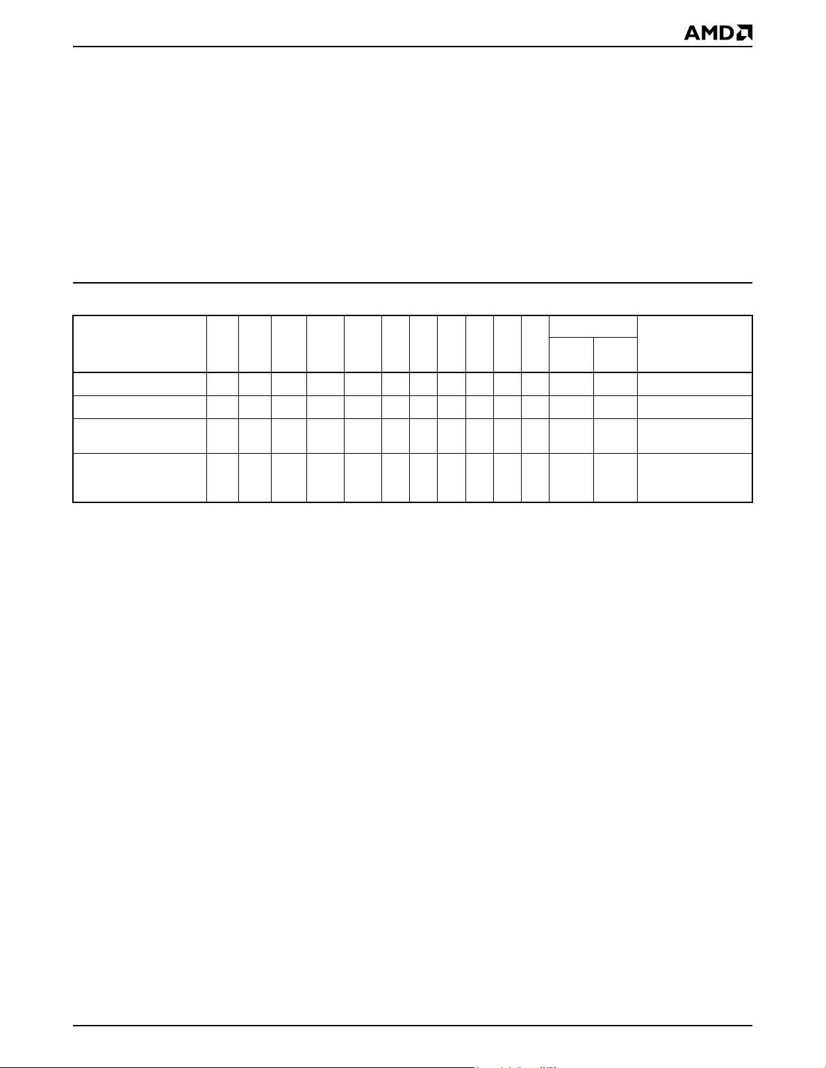
Device Bus Operations . . . . . . . . . . . . . . . . . . . . . 10
Table 1. Am29DS163D Device Bus Operations .............................10
Word/Byte Configuration ........................................................10
Requirements for Reading Array Data ...................................10
Writing Commands/Command Sequences ............................11
Accelerated Program Operation ......................................................11
Autoselect Function s ........................... ................ ................ ............11
Simultaneous Read/Write Operations with Zero Latency .......11
Standby Mode ........................................................................11
Automatic Sleep Mode .................................... .. .....................12
RESET#: Hardware Reset Pin ...............................................12
Output Disable Mode ..............................................................12
Table 2. Am29DS163D Device Bank Divisions ...............................12
Table 3. Top Boot Sector Addresses (Am29DS16xDT) ..................13
SecSi Sector Addresses for Top Boot Device s.............................. 13
Table 5. Bottom Boot Sector Addresses (Am29DS16xDB) ............14
SecSi Sector Addresses for Botto m Boot Device s................. ........ 14
Autoselect Mode ............................................ .. .......................15
Table 7. Am29DS163D Autoselect Codes (High Voltage Method) 15
Sector/Sector Block Protection and Unprotection ..................16
Table 8. Top Boot Sector/Sector Block Addresses
for Protection/Unpro tection ............................... ................ ..............16
Table 9. Bottom Boot Sector/Sector Block Addresses
for Protection/Unpro tection ............................... ................ ..............16
Write Protect (WP#) ................................................................17
Temporary Sector/Sector Block Unprotect .............................17
Figure 1. Temporary Sector Unprotect Operation........................... 17
Figure 2. In-System Sector/Sector Block Protect
and Unprotect Algorithms. ................ ................................ ............... 18
SecSi (Secured Silicon) Sector Flash Memory Region ..........19
Hardware Data Protection ......................................................19
Low VCC Write Inhibit .....................................................................20
Write Pulse “Glitch” Protection ................... ................................ .....20
Logical Inhibit ..................................................................................20
Power-Up Write Inhibit ............... ................................................ .....20
Common Flash Memory Interface (CFI) . . . . . . . 20
Table 10. CFI Query Identification String........................................ 20
System Interface String........................ ................ ........................... 21
Table 12. Device Geometry Definit ion.................... ........................ 21
Table 13. Primary Vendor-Specific Extended Query ...................... 22
Command Definitions . . . . . . . . . . . . . . . . . . . . . . 23
Reading Array Data ................................................................23
Reset Command .....................................................................23
Autoselect Command Sequence ......................... ...................23
Enter SecSi Sector/Exit SecSi Sector Command Sequence ..24
Byte/Word Program Command Sequence .............................24
Unlock Bypass Command Sequence ..............................................24
Figure 3. Program Operat io n.................... ................................ ...... 25
Chip Erase Command Sequence ...........................................25
Sector Erase Command Sequence ...................... .. ................25
Erase Suspend/Erase Resume Commands ........................... 26
Figure 4. Erase Operation............. ................ ................................ . 26
Table 14. Am29DS163D Command Defin itions........................ ...... 27
Write Operation Status . . . . . . . . . . . . . . . . . . . . 28
DQ7: Data# Po l lin g .......... ... .. .............. .. ... .............. .. ... ............28
Figure 5. Data# Polling Algorithm................................................. . 28
RY/BY#: Ready/Busy# ............................................................ 29
DQ6: Toggle Bit I ....................................................................29
Figure 6. Toggle Bit Algorithm........................................................ 29
DQ2: Toggle Bit II ...................................................................30
Reading Toggle Bits DQ6/DQ2 ...............................................30
DQ5: Exceeded Timing Limits ................................................30
DQ3: Sector Era s e Time r ............ ...........................................30
Table 15. Write Operation Sta tus ............. ................ ......................31
Absolute Maximum Ratings . . . . . . . . . . . . . . . . 32
Figure 7. Maximum Negative Overshoot Waveform...................... 32
Figure 8. Maximum Positive Overshoot Waveform....................... 32
Operating Ranges . . . . . . . . . . . . . . . . . . . . . . . . . 32
DC Characteristics . . . . . . . . . . . . . . . . . . . . . . . . 33
Figure 9. I
and Automatic Sleep Currents)...................................................... 34
Figure 10. Typical I
Current vs. Time (Showing Active
CC1
vs. Frequency.............. ................ .............. 34
CC1
Test Conditions . . . . . . . . . . . . . . . . . . . . . . . . . . 35
Figure 11. Test Setup..................... ................. ................ .............. 35
Table 16. Test Specifications ................... ................ ................ ......35
Figure 12. Input Waveforms and Measurement Levels ................. 35
AC Characteristics . . . . . . . . . . . . . . . . . . . . . . . . 36
Figure 13. Read Operation Timings. ........ .............................. ........ 36
Figure 14. Reset Timings............................................................... 37
Word/Byte Configuration (BYTE#) ..........................................38
Figure 15. BYTE# Timings for Read Operations............................ 38
Figure 16. BYTE# Timings for Write Operations............................ 38
Erase and Program Operations .............................................. 39
Figure 17. Program Operation Timings.......................................... 40
Figure 18. Accelerated Program Timing Diagram.......................... 40
Figure 19. Chip/Sector Erase Operation Timings.......................... 41
Figure 20. Back-to-back Read/Write Cycle Timings ...................... 42
Figure 21. Data# Polling Timings (During Embedded Algorithms) . 42
Figure 22. Toggle Bit Timings (During Embedded Algorithms)...... 43
Figure 23. DQ2 vs. DQ6............................ ................................ ..... 43
Temporary Sector/Sector Block Unprotect .............................44
Figure 24. Temporary Sector/Sector Block
Unprotect Timing Diagr a m.............. ................. ................ .............. 44
Figure 25. Sector/Sector Block Protect/Unprotect Timing Diagram 45
Alternate CE# Controlled Erase and Program O perations .....46
Figure 26. Alternate CE# Controlled Write
(Erase/Program) Operati o n Timings............. ................................ . 47
Erase And Programming Performance . . . . . . . 48
Latchup Characteristics . . . . . . . . . . . . . . . . . . . . 48
Data Retention. . . . . . . . . . . . . . . . . . . . . . . . . . . . 48
Physical Dimensions . . . . . . . . . . . . . . . . . . . . . . 49
FBA048—48-Ball Fine-Pitch Ball Grid Array (FBGA)
6 x 8 mm package ...................................................... ...........49
Revision Summary . . . . . . . . . . . . . . . . . . . . . . . . 50
Am29DS163D 5
Page 6
ADVANCE INFORMATION
PRODUCT SELECTOR GUIDE
Part Number Am29DS163D
Speed Option Standard Voltage Range: VCC = 1.8–2.2 V 100 120
Max Access Time (ns) 100 120
CE# Access (ns) 100 120
OE# Access (ns) 35 50
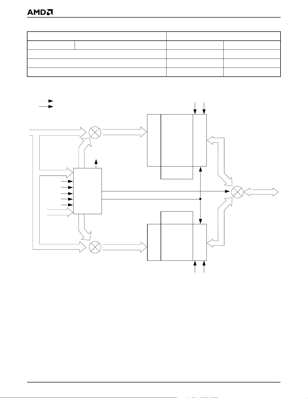
BLOCK DIAGRAM
V
CC
V
SS
OE# BYTE#
A0–A19
A0–A19
RESET#
WE#
CE#
BYTE#
WP#/ACC
DQ0–DQ15
A0–A19
RY/BY#
A0–A19A0–A19
STATE
CONTROL
&
COMMAND
REGISTER
Upper Bank Address
Lower Bank Address
Y-Decoder
Status
Control
Y-Decoder
Upper Bank
X-Decoder
X-Decoder
Lower Bank
Latches and Control Logic
Latches and
Control Logic
OE# BYTE#
DQ0–DQ15
DQ0–DQ15 DQ0–DQ15
6 Am29DS163D
Page 7
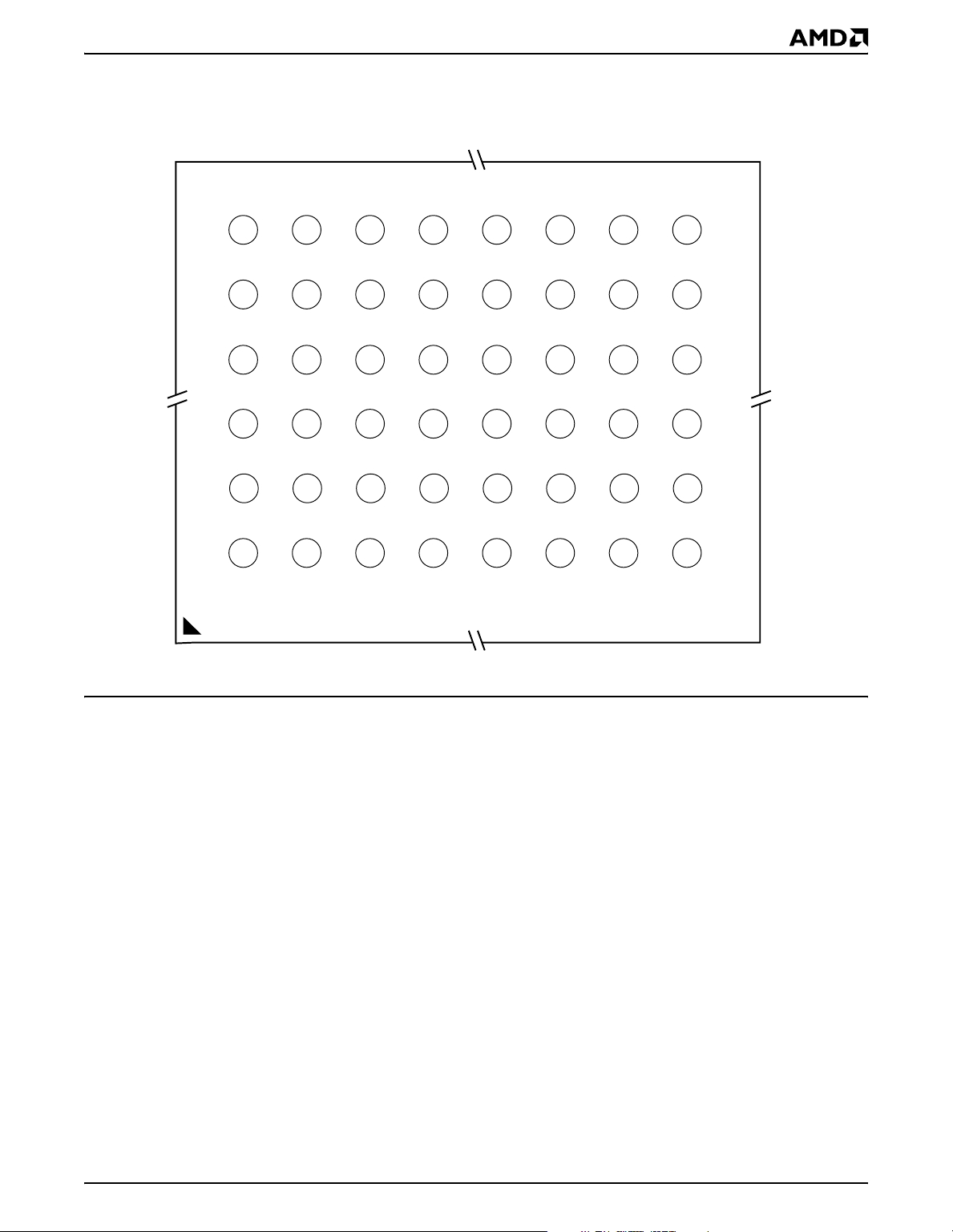
CONNECTION DIAGRAMS
A6 B6 C6 D6 E6 F6 G6 H6
A5 B5 C5 D5 E5 F5 G5 H5
A4 B4 C4 D4 E4 F4 G4 H4
A3 B3 C3 D3 E3 F3 G3 H3
A2 B2 C2 D2 E2 F2 G2 H2
ADVANCE INFORMATION
48-Ball FBGA
Top View, Balls Facing Down
BYTE#A16A15A14A12A13
DQ15/A-1
DQ13 DQ6DQ14DQ7A11A10A8A9
V
CC
DQ11 DQ3DQ10DQ2NCA18WP#/ACCRY/BY#
DQ9 DQ1DQ8DQ0A5A6A17A7
V
SS
DQ4DQ12DQ5A19NCRESET#WE#
A1 B1 C1 D1 E1 F1 G1 H1
Special Handling Instructions for FBGA
Package
Special handling is required for Flash Memory products in FBGA packages.
CE#A0A1A2A4A3
OE#
V
SS
Flash memory devices in FBGA packages may be
damaged if exposed to ultrasonic cleaning methods.
The package and/or data integrity may be compromised if the package body is exposed to temperatures
above 150°C for prolonged periods of time.
Am29DS163D 7
Page 8
ADVANCE INFORMATION
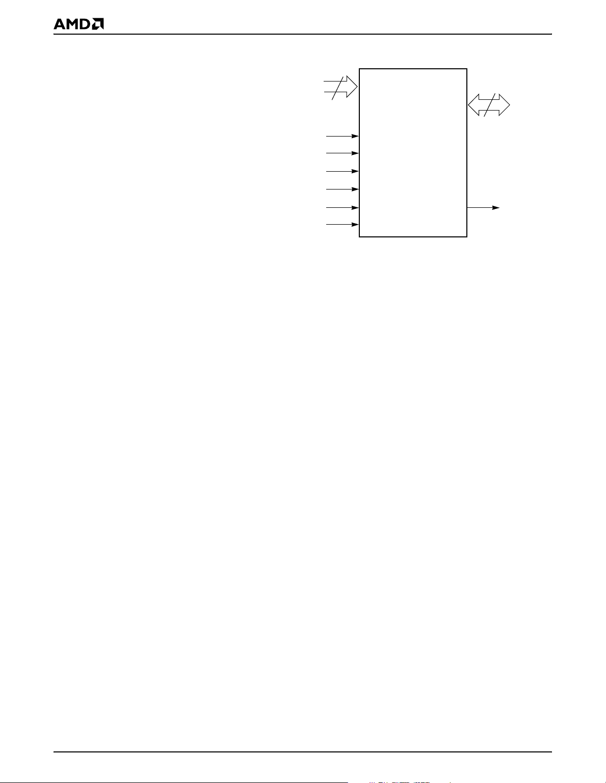
PIN DESCRIPTION
A0–A19 = 20 Addresses
DQ0–DQ14 = 15 Data Inputs/Outputs
DQ15/A-1 = DQ15 (Data Input/Output, word
mode), A-1 (LSB Address Input, byte
mode)
CE# = Chip Enable
OE# = Output Enable
WE# = Write Enable
WP#/ACC = Hardware Write Protect/
Acceleration Pin
RESET# = Hardware Reset Pin, Active Low
BYTE# = Selects 8-bit or 16-bit mode
RY/BY# = Ready/Busy Output
VCC = 1.8 volt-only single power supply
(see Product Selector Guide for speed
options and voltage supply tolerances)
V
SS
NC = Pin Not Connected Internally
= Device Ground
LOGIC SYMBOL
20
A0–A19
CE#
OE#
WE#
WP#/ACC
RESET#
BYTE#
16 or 8
DQ0–DQ15
(A-1)
RY/BY#
8 Am29DS163D
Page 9
ADVANCE INFORMATION
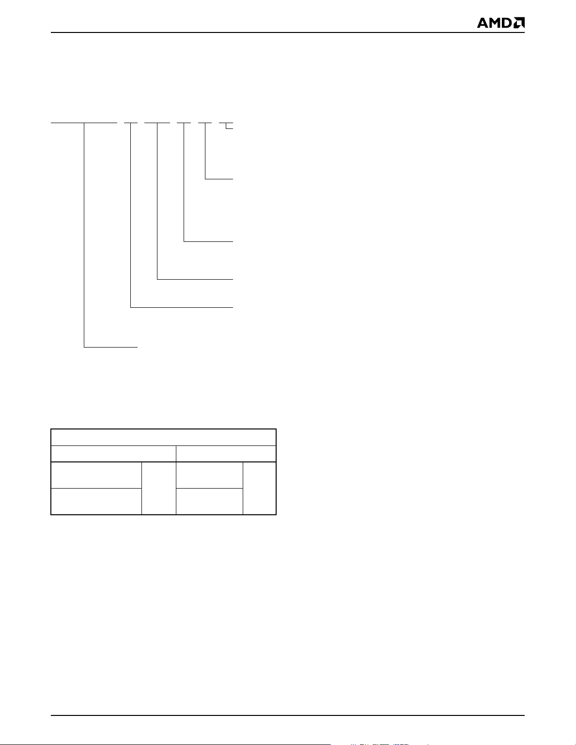
ORDERING INFORMATION
Standard Products
AMD standard products are available in several packages and operating ranges. The order number (Valid
Combination) is formed by a combination of the following:
Am29DS163D T 100 E I
OPTIONAL PROCESSING
Blank = Standard Processing
N = 16-byte ESN devices
(Contact an AMD representative for more information)
TEMPERATURE RANGE
I = Industrial (–40°C to +85°C)
E = Extended (–55°C to +125°C)
F = Industrial (-40oC to +85oC) with Pb-free Package
K = Extended (-55oC to +125oC) with Pb-free Package
PACKAGE TYPE
WA = 48-Ball Fine-Pitch Ball Grid Array (FBGA)
0.80 mm pitch, 6 x 8 mm package (FBA048)
SPEED OPTION
See Product Selector Guide and Valid Combinations
Valid Combinations for FBGA Packages
Order Number Package Marking
Am29DS163DT100,
Am29DS163DB100
Am29DS163DT120,
Am29DS163DB120
BOOT CODE SECTOR ARCHITECTURE
T = Top sector
B = Bottom sector
DEVICE NUMBER/DESCRIPTION
Am29DS163D
16Megabit (2 M x 8-Bit/1 M x 16-Bit) CMOS Flash Memory
1.8 Volt-only Read, Program, and Erase
Valid Combinations list configurations planned to be supported in
volume for this device. Consult the local AMD sales office to con
WAI,
WAE,
WAF,
WAK
S163DT10V,
S163DB10V
S163DT12V,
S163DB12V
I, E,
F, K
firm availability of specific valid combinations and to check on
newly released combinations.
Valid Combinations
-
Am29DS163D 9
Page 10
ADVANCE INFORMATION
DEVICE BUS OPERATIONS
This section describes the requirements and use of
the device bus operations, which are initiated through
the internal command register. The command register
itself does not occupy any addressable memory location. The register is a latch used to store the
commands, along with the address and data informa
tion needed to execute the command. The contents of
Tab l e 1. Am29DS163D Device Bus Operations
-
the register serve as inputs to the internal state machine. The state machine outputs dictate the function
of the device. Tab l e 1 lists the device bus operations,
the inputs and control levels they require, and the resulting output. The following subsections describe
each of these operations in further detail.
DQ8–DQ15
Addresses
Operation CE# OE# WE# RESET# WP#/ACC
(Note 2)
Read L L H H L/H A
Write L H L H (Note 3) A
Standby
VCC ±
0.3 V
X X
VCC ±
0.3 V
H X High-Z High-Z High-Z
IN
IN
DQ0–
DQ7
D
OUT
D
IN
BYTE#
= V
IH
D
OUT
D
IN
BYTE#
= V
IL
DQ8–DQ14 = High-Z,
DQ15 = A-1
Output Disable L H H H L/H X High-Z High-Z High-Z
Reset X X X L L/H X High-Z High-Z High-Z
Sector Protect (Note 2) L H L V
Sector Unprotect (Note 2) L H L V
Temporary Sector Unprotect X X X V
ID
ID
ID
L/H
(Note 3)
(Note 3) A
SA, A6 = L,
A1 = H, A0 = L
SA, A6 = H,
A1 = H, A0 = L
IN
D
IN
D
IN
D
IN
X X
X X
D
IN
High-Z
Legend: L = Logic Low = VIL, H = Logic High = VIH, VID = 9.0–11.0 V, VHH = 9.0 ± 0.5 V, X = Don’t Care, SA = Sector Address,
A
= Address In, DIN = Data In, D
IN
= Data Out
OUT
Notes:
1. Addresses are A19:A0 in word mode (BYTE# = VIH), A19:A-1 in byte mode (BYTE# = VIL).
2. The sector protect and sector unprotect functions may also be implemented via programming equipment. See “Sector/Sector
Block Protection and Unprotection” on page 16.
3. If WP#/ACC = VIL, the two outermost boot sectors remain protected. If WP#/ACC = VIH, the two outermost boot sector
protection depends on whether they were last protected or unprotected using the method described in
Protection and Unprotection” on page 16. If WP#/ACC = V
all sectors are unprotected.
HH,
“Sector/Sector Block
Word/Byte Configuration
The BYTE# pin controls whether the device data I/O
pins operate in the byte or word configuration. If the
BYTE# pin is set at logic ‘1’, the device is in word configuration, DQ0–DQ15 are active and controlled by
CE# and OE#.
If the BYTE# pin is set at logic ‘0’, the device is in byte
configuration, and only data I/O pins DQ0–DQ7 are
active and controlled by CE# and OE#. The data I/O
pins DQ8–DQ14 are tri-stated, and the DQ15 pin is
used as an input for the LSB (A-1) address function.
Requirements for Reading Array Data
To read array data from the outputs, the system must
drive the CE# and OE# pins to VIL. CE# is the power
control and selects the device. OE# is the output control and gates array data to the output pins. WE#
should remain at VIH. The BYTE# pin determines
whether the device outputs array data in words or
bytes.
The internal state machine is set for reading array data
upon device power-up, or after a hardware reset. This
ensures that no spurious alteration of the memory
content occurs during the power transition. No com
mand is necessary in this mode to obtain array data.
Standard microprocessor read cycles that assert valid
10 Am29DS163D
-
Page 11

ADVANCE INFORMATION
addresses on the device address inputs produce valid
data on the device data outputs. Each bank remains
enabled for read access until the command register
contents are altered.
See “Requirements for Reading Array Data” on
page 10 for more information. Refer to the Ta bl e on
page 36 for timing specifications and to Figure 13, on
page 36 for the timing diagram. I
in the DC Charac-
CC1
teristics table represents the active current
specification for reading array data.
Writing Commands/Command Sequences
To write a command or command sequence (which includes programming data to the device and erasing
sectors of memory), the system must drive WE# and
CE# to V
For program operations, the BYTE# pin determines
whether the device accepts program data in bytes or
words. Refer to “Word/Byte Configuration” on page 10
for more information.
The device features an Unlock Bypass mode to facili-
tate faster programming. Once a bank enters the
Unlock Bypass mode, only two write cycles are required to program a word or byte, instead of four. The
“Word/Byte Configuration” section contains details on
programming data to the device using both standard
and Unlock Bypass command sequences.
An erase operation can erase one sector, multiple sectors, or the entire device. Table 3 on page 13 to
Tab l e 6 on page 14 indicate the address space that
each sector occupies. The device address space is divided into two banks: Bank 1 contains the
boot/parameter sectors, and Bank 2 contains the
larger, code sectors of uniform size. A “bank address”
is the address bits required to uniquely select a bank.
Similarly, a “sector address” is the address bits required to uniquely select a sector.
I
CC2
tive current specification for the write mode. The “AC
Characteristics” on page 36 section contains timing
specification tables and timing diagrams for write
operations.
Accelerated Program Operation
The device offers accelerated program operations
through the ACC function. This is one of two functions
provided by the WP#/ACC pin. This function is primarily intended to allow faster manufacturing throughput
at the factory.
If the system asserts VHH on this pin, the device automatically enters the aforementioned Unlock Bypass
mode, temporarily unprotects any protected sectors,
and uses the higher voltage on the pin to reduce the
time required for program operations. The system
, and OE# to VIH.
IL
in the DC Characteristics table represents the ac-
would use a two-cycle program command sequence
as required by the Unlock Bypass mode. Removing
V
from the WP#/ACC pin returns the device to nor-
HH
mal operation. Note that the WP#/ACC pin must not be
at VHH for operations other than accelerated programming, or device damage may result. In addition, the
WP#/ACC pin must not be left floating or unconnected;
inconsistent behavior of the device may result.
Autoselect Functions
If the system writes the autoselect command sequence, the device enters the autoselect mode. The
system can then read autoselect codes from the inter
nal register (which is separate from the memory array)
on DQ7–DQ0. Standard read cycle timings apply in
this mode. Refer to
“Autoselect Mode” on page 15 and
“Autoselect Command Sequence” on page 23 for
more information.
Simultaneous Read/Write Operations with
Zero
Latency
This device is capable of reading data from one bank
of memory while programming or erasing in the other
bank of memory. An erase operation may also be suspended to read from or program to another location
within the same bank (except the sector being
erased). Figure 20, on page 42 shows how read and
write cycles may be initiated for simultaneous operation with zero latency. I
CC6
and I
in the DC
CC7
Characteristics table represent the current specifications for read-while-program and read-while-erase,
respectively.
Standby Mode
When the system is not reading or writing to the device, it can place the device in the standby mode. In
this mode, current consumption is greatly reduced,
and the outputs are placed in the high impedance
state, independent of the OE# input.
The device enters the CMOS standby mode when the
CE# and RESET# pins are both held at VCC ± 0.3 V.
(Note that this is a more restricted voltage range than
VIH.) If CE# and RESET# are held at VIH, but not within
VCC ± 0.3 V, the device is in the standby mode, but the
standby current is greater. The device requires standard access time (tCE) for read access when the
device is in either of these standby modes, before it is
ready to read data.
If the device is deselected during erasure or programming, the device draws active current until the
operation is completed.
I
in the DC Characteristics table represents the
CC3
standby current specification.
-
Am29DS163D 11
Page 12
ADVANCE INFORMATION
Automatic Sleep Mode
The automatic sleep mode minimizes Flash device energy consumption. The device automatically enables
this mode when addresses remain stable for t
ACC
+
30 ns. The automatic sleep mode is independent of
the CE#, WE#, and OE# control signals. Standard ad
dress access timings provide new data when
addresses are changed. While in sleep mode, output
data is latched and always available to the system.
I
in the “DC Characteristics” on page 33 represents
CC4
the automatic sleep mode current specification.
RESET#: Hardware Reset Pin
The RESET# pin provides a hardware method of resetting the device to reading array data. When the
RESET# pin is driven low for at least a period of t
the device immediately terminates any operation in
progress, tristates all output pins, and ignores all
read/write commands for the duration of the RESET#
pulse. The device also resets the internal state ma
chine to reading array data. The operation that was
interrupted should be reinitiated once the device is
ready to accept another command sequence, to en
sure data integrity.
Current is reduced for the duration of the RESET#
pulse. When RESET# is held at V
draws CMOS standby current (I
±0.3 V, the device
SS
). If RESET# is held
CC4
RP
,
-
-
at V
but not within VSS±0.3 V, the standby current is
IL
greater.
The RESET# pin may be tied to the system reset circuitry. A system reset would thus also reset the Flash
memory, enabling the system to read the boot-up firmware from the Flash memory.
If RESET# is asserted during a program or erase operation, the RY/BY# pin remains a “0” (busy) until the
internal reset operation is complete, which requires a
time of t
(during Embedded Algorithms). The sys-
READY
tem can thus monitor RY/BY# to determine whether
the reset operation is complete. If RESET# is asserted
when a program or erase operation is not executing
(RY/BY# pin is “1”), the reset operation is completed
within a time of t
(not during Embedded Algo-
READY
rithms). The system can read data tRH after the
RESET# pin returns to VIH.
Refer to “AC Characteristics” on page 36 for RESET#
parameters and to Figure 14, on page 37 for the timing
diagram.
Output Disable Mode
When the OE# input is at VIH, output from the device is
disabled. The output pins are placed in the high
impedance state.
Device
Part Number
Am29DS163D 4 Mbit
Megabits Sector Sizes Megabits Sector Sizes
Table 2. Am29DS163D Device Bank Divisions
Bank 1 Bank 2
Eight 8 Kbyte/4 Kword,
seven 64 Kbyte/32 Kword
12 Mbit
Twenty-four
64 Kbyte/32 Kword
12 Am29DS163D
Page 13
ADVANCE INFORMATION
Table 3. Top Boot Sector Addresses (Am29DS16xDT)
Sector
Am29DS163DT
Bank 2
Bank 1
Note: The address range is A19:A-1 in byte mode (BYTE#=VIL) or A19:A0 in word mode (BYTE#=VIH). The bank address bits are A19 and A18 for
Am29DS163DT.
SA0 00000xxx 64/32 000000h-00FFFFh 00000h–07FFFh
SA1 00001xxx 64/32 010000h-01FFFFh 08000h–0FFFFh
SA2 00010xxx 64/32 020000h-02FFFFh 10000h–17FFFh
SA3 00011xxx 64/32 030000h-03FFFFh 18000h–1FFFFh
SA4 00100xxx 64/32 040000h-04FFFFh 20000h–27FFFh
SA5 00101xxx 64/32 050000h-05FFFFh 28000h–2FFFFh
SA6 00110xxx 64/32 060000h-06FFFFh 30000h–37FFFh
SA7 00111xxx 64/32 070000h-07FFFFh 38000h–3FFFFh
SA8 01000xxx 64/32 080000h-08FFFFh 40000h–47FFFh
SA9 01001xxx 64/32 090000h-09FFFFh 48000h–4FFFFh
SA10 01010xxx 64/32 0A0000h-0AFFFFh 50000h–57FFFh
SA11 01011xxx 64/32 0B0000h-0BFFFFh 58000h–5FFFFh
SA12 01100xxx 64/32 0C0000h-0CFFFFh 60000h–67FFFh
SA13 01101xxx 64/32 0D0000h-0DFFFFh 68000h–6FFFFh
SA14 01110xxx 64/32 0E0000h-0EFFFFh 70000h–77FFFh
SA15 01111 xxx 64/32 0F0000h-0FFFFFh 78000h–7FFFFh
SA16 10000xxx 64/32 100000h-10FFFFh 80000h–87FFFh
SA17 10001xxx 64/32 110000h-11FFFFh 88000h–8FFFFh
SA18 10010xxx 64/32 120000h-12FFFFh 90000h–97FFFh
SA19 10011xxx 64/32 130000h-13FFFFh 98000h–9FFFFh
SA20 10100xxx 64/32 140000h-14FFFFh A0000h–A7FFFh
SA21 10101xxx 64/32 150000h-15FFFFh A8000h–AFFFFh
SA22 10110xxx 64/32 160000h-16FFFFh B0000h–B7FFFh
SA23 10111xxx 64/32 170000h-17FFFFh B8000h–BFFFFh
SA24 11000xxx 64/32 180000h-18FFFFh C0000h–C7FFFh
SA25 11001xxx 64/32 190000h-19FFFFh C8000h–CFFFFh
SA26 11010xxx 64/32 1A0000h-1AFFFFh D0000h–D7FFFh
SA27 11011xxx 64/32 1B0000h-1BFFFFh D8000h–DFFFFh
SA28 11100xxx 64/32 1C0000h-1CFFFFh E0000h–E7FFFh
SA29 11101xxx 64/32 1D0000h-1DFFFFh E8000h–EFFFFh
SA30 11110 xxx 64/32 1E0000h-1EFFFFh F0000h–F7FFFh
SA31 11111000 8/4 1F0000h-1F1FFFh F8000h–F8FFFh
SA32 11111001 8/4 1F2000h-1F3FFFh F9000h–F9FFFh
SA33 11111010 8/4 1F4000h-1F5FFFh FA000h–FAFFFh
SA34 111110 11 8/4 1F6000h-1F7FFFh FB000h–FBFFFh
SA35 1111110 0 8/4 1F8000h-1F9FFFh FC000h–FCFFFh
SA36 1111110 1 8/4 1FA000h-1FBFFFh FD000h–FDFFFh
SA37 1111111 0 8/4 1FC000h-1FDFFFh FE000h–FEFFFh
SA38 11111111 8/4 1FE000h-1FFFFFh FF000h–FFFFFh
Sector Address
A19–A12
Sector Size
(Kbytes/Kwords)
(x8)
Address Range
(x16)
Address Ranges
Table 4. SecSi Sector Addresses for Top Boot Devices
SecSi Sector
Entire Sector
Factory Programmed ESN 11111xxx 16 bytes/8 words 1F0000h-1F000Fh F8000h–F8007h
Sector Address
A19–A12
11111xxx 64 Kbytes/32 Kwords 1F0000h-1FFFFFh F8000h–FFFFFh
Size
(x8)
Address Range
(x16)
Address Range
Am29DS163D 13
Page 14
ADVANCE INFORMATION
Table 5. Bottom Boot Sector Addresses (Am29DS16xDB)
Sector
Am29DS163DB
Bank 1
Bank 2
Note: The address range is A19:A-1 in byte mode (BYTE#=VIL) or A19:A0 in word mode (BYTE#=VIH). The bank address bits are A19 and A18 for
Am29DS163DB.
SA0 00000000 8/4 000000h-001FFFh 00000h-00FFFh
SA1 00000001 8/4 002000h-003FFFh 01000h-01FFFh
SA2 00000010 8/4 004000h-005FFFh 02000h-02FFFh
SA3 00000011 8/4 006000h-007FFFh 03000h-03FFFh
SA4 00000100 8/4 008000h-009FFFh 04000h-04FFFh
SA5 00000101 8/4 00A000h-00BFFFh 05000h-05FFFh
SA6 00000110 8/4 00C000h-00DFFFh 06000h-06FFFh
SA7 00000111 8/4 00E000h-00FFFFh 07000h-07FFFh
SA8 00001XXX 64/32 010000h-01FFFFh 08000h-0FFFFh
SA9 00010XXX 64/32 020000h-02FFFFh 10000h-17FFFh
SA10 00011XXX 64/32 030000h-03FFFFh 18000h-1FFFFh
SA11 00100XXX 64/32 040000h-04FFFFh 20000h-27FFFh
SA12 00101XXX 64/32 050000h-05FFFFh 28000h-2FFFFh
SA13 00110XXX 64/32 060000h-06FFFFh 30000h-37FFFh
SA14 00111XXX 64/32 070000h-07FFFFh 38000h-3FFFFh
SA15 01000XXX 64/32 080000h-08FFFFh 40000h-47FFFh
SA16 01001XXX 64/32 090000h-09FFFFh 48000h-4FFFFh
SA17 01010XXX 64/32 0A0000h-0AFFFFh 50000h-57FFFh
SA18 01011XXX 64/32 0B0000h-0BFFFFh 58000h-5FFFFh
SA19 01100XXX 64/32 0C0000h-0CFFFFh 60000h-67FFFh
SA20 01101XXX 64/32 0D0000h-0DFFFFh 68000h-6FFFFh
SA21 0 1110X XX 64/32 0E0000h-0EFFFFh 70000h-77FFFh
SA22 01111XXX 64/32 0F0000h-0FFFFFh 78000h-7FFFFh
SA23 10000XXX 64/32 100000h-10FFFFh 80000h-87FFFh
SA24 10001XXX 64/32 110000h-11FFFFh 88000h-8FFFFh
SA25 10010XXX 64/32 120000h-12FFFFh 90000h-97FFFh
SA26 10011XXX 64/32 130000h-13FFFFh 98000h-9FFFFh
SA27 10100XXX 64/32 140000h-14FFFFh A0000h-A7FFFh
SA28 10101XXX 64/32 150000h-15FFFFh A8000h-AFFFFh
SA29 10110XXX 64/32 160000h-16FFFFh B0000h-B7FFFh
SA30 10111XXX 64/32 170000h-17FFFFh B8000h-BFFFFh
SA31 11000XXX 64/32 180000h-18FFFFh C0000h-C7FFFh
SA32 11001XXX 64/32 190000h-19FFFFh C8000h-CFFFFh
SA33 11010XXX 64/32 1A0000h-1AFFFFh D0000h-D7FFFh
SA34 11011XXX 64/32 1B0000h-1BFFFFh D8000h-DFFFFh
SA35 111 00X XX 64/32 1C0000h-1CFFFFh E0000h-E7FFFh
SA36 111 01X XX 64/32 1D0000h-1DFFFFh E8000h-EFFFFh
SA37 11110 XX X 64/32 1E0000h-1EFFFFh F0000h-F7FFFh
SA38 11111 XXX 64/32 1F0000h-1FFFFFh F8000h-FFFFFh
Sector Address
A19–A12
Sector Size
(Kbytes/Kwords)
(x8)
Address Range
(x16)
Address Range
Table 6. SecSi Sector Addresses for Bottom Boot Devices
SecSi Sector
Entire Sector 00000XXX 64 Kbytes/32 Kwords 000000h-00FFFFh 00000h-07FFFh
Factory Programmed ESN 00000XXX 16 bytes/8 words 000000h-00000Fh 00000h–00007h
Sector Address
A19–A12
Size
(x8)
Address Range
14 Am29DS163D
(x16)
Address Range
Page 15
ADVANCE INFORMATION
Autoselect Mode
The autoselect mode provides manufacturer and device identification, and sector protection verification,
through identifier codes output on DQ7–DQ0. This
mode is primarily intended for programming equipment to automatically match a device to be
programmed with its corresponding programming al
gorithm. However, the autoselect codes can also be
accessed in-system through the command register.
When using programming equipment, the autoselect
mode requires VID (9.0 V to 11.0 V) on address pin A9.
Address pins A6, A1, and A0 must be as shown in
Table 7. Am29DS163D Autoselect Codes (High Voltage Method)
A19
to
Description CE# OE# WE#
Manufacturer ID: AMD L L H BA X
Device ID: Am29DS163D L L H BA X
Sector Protection
Verification
SecSi Sector Indicator Bit
(DQ7)
L L H SA X
L L H BA X
A12
-
A11
to
A10 A9
V
V
V
V
Table 7. In addition, when verifying sector protection,
the sector address must appear on the appropriate
highest order address bits (see Tables 3–6). Ta b l e 7
shows the remaining address bits that are don’t care.
When all necessary bits are set as required, the programming equipment may then read the
corresponding identifier code on DQ7–DQ0.
To access the autoselect codes in-system, the host
system can issue the autoselect command via the
command register, as shown in Table 14. This method
does not require VID. Refer to the Autoselect Command Sequence section for more information.
A8
to
A7
X L X L L X X 01h
ID
X L X L H 22h X 95h (T), 96h (B)
ID
X L X H L X X
ID
X L X H H X X
ID
A6
A5
to
A2
A1 A0
DQ8 to DQ15
BYTE#
= V
IH
BYTE#
= V
IL
01h (protected),
00h (unprotected)
85h (factory locked),
05h (not factory
locked)
DQ7
DQ0
to
Legend: T = Top Boot Block, B = Bottom Boot Block, L = Logic Low = VIL, H = Logic High = VIH, BA = Bank Address, SA =
Sector Address, X = Don’t care.
Am29DS163D 15
Page 16

ADVANCE INFORMATION
Sector/Sector Block Protection and Unprotection
(Note: For the following discussion, the term “sector”
applies to both sectors and sector blocks. A sector
block consists of two or more adjacent sectors that are
protected or unprotected at the same time (see Tables
8 and 9).
Table 8. Top Boot Sector/Sector Block Addresses
for Protection/Unprotection
Sector / Sector
Block
SA0 00000XXX 64 Kbytes
SA1-SA3
SA4-SA7 001XXXXX 256 (4x64) Kbytes
SA8-SA11 010XXXXX 256 (4x64) Kbytes
SA12-SA15 011XXXXX 256 (4x64) Kbytes
SA16-SA19 100XXXXX 256 (4x64) Kbytes
SA20-SA23 101XXXXX 256 (4x64) Kbytes
SA24-SA27 110XXXXX 256 (4x64) Kbytes
SA28-SA30
SA31 11111000 8 Kbytes
SA32 11111001 8 Kbytes
SA33 11111010 8 Kbytes
SA34 111110 11 8 Kbytes
SA35 1111110 0 8 Kbytes
SA36 1111110 1 8 Kbytes
SA37 1111111 0 8 Kbytes
SA38 11111111 8 Kbytes
A19–A12 Sector / Sector Block Size
00001XXX,
00010XXX,
00011XXX
11100XXX,
11101XXX,
11110 XX X
192 (3x64) Kbytes
192 (3x64) Kbytes
Table 9. Bottom Boot Sector/Sector Block
Addresses for Protection/Unprotection
Sector / Sector
Block
SA38 11111X XX 64 Kbytes
SA37-SA35
SA34-SA31 110XXXXX 256 (4x64) Kbytes
SA30-SA27 101XXXXX 256 (4x64) Kbytes
SA26-SA23 100XXXXX 256 (4x64) Kbytes
SA22-SA19 011XXXXX 256 (4x64) Kbytes
SA18-SA15 010XXXXX 256 (4x64) Kbytes
SA14-SA11 001XXXXX 256 (4x64) Kbytes
SA10-SA8
SA7 00000111 8 Kbytes
SA6 00000110 8 Kbytes
SA5 00000101 8 Kbytes
SA4 00000100 8 Kbytes
SA3 00000011 8 Kbytes
SA2 00000010 8 Kbytes
SA1 00000001 8 Kbytes
SA0 00000000 8 Kbytes
A19–A12 Sector / Sector Block Size
11110 XX X,
11101XXX,
11100XXX
00001XXX,
00010XXX,
00011XXX
192 (3x64) Kbytes
192 (3x64) Kbytes
The hardware sector protection feature disables both
program and erase operations in any sector. The hardware sector unprotection feature re-enables both
program and erase operations in previously protected
sectors. Sector protection and unprotection can be implemented via two methods.
The primary method requires VID on the RESET# pin
only, and can be implemented either in-system or via
programming equipment. Figure 2 shows the algo-
rithms and Figure 25 shows the timing diagram. This
method uses standard microprocessor bus cycle timing. For sector unprotect, all unprotected sectors must
first be protected prior to the first sector unprotect
write cycle.
16 Am29DS163D
Page 17

ADVANCE INFORMATION
The alternate method intended only for programming
equipment requires VID on address pin A9 and OE#.
This method is compatible with programmer routines
written for earlier 1.8 volt-only AMD flash devices.
Contact an AMD representative for further details.
The device is shipped with all sectors unprotected.
AMD offers the option of programming and protecting
sectors at its factory prior to shipping the device
through AMD’s ExpressFlash™ Service. Contact an
AMD representative for details.
It is possible to determine whether a sector is protected or unprotected. See the Autoselect Mode
section for details.
Write Protect (WP#)
The Write Protect function provides a hardware
method of protecting certain boot sectors without
using V
WP#/ACC pin.
If the system asserts VIL on the WP#/ACC pin, the device disables program and erase functions in the two
“outermost” 8 Kbyte boot sectors independently of
whether those sectors were protected or unprotected
using the method described in
Protection and Unprotection”. The two outermost 8
Kbyte boot sectors are the two sectors containing the
lowest addresses in a bottom-boot-configured device,
or the two sectors containing the highest addresses in
a top-boot-configured device.
. This function is one of two provided by the
ID
“Sector/Sector Block
block consists of two or more adjacent sectors that are
protected or unprotected at the same time (see Tables
8 and 9).
This feature allows temporary unprotection of previously protected sectors to change data in-system. The
Sector Unprotect mode is activated by setting the RE
SET# pin to VID (9.0 – 11.0 V). During this mode,
formerly protected sectors can be programmed or
erased by selecting the sector addresses. Once VID is
removed from the RESET# pin, all the previously protected sectors are protected again. Figure 1 shows the
algorithm, and Figure 24 shows the timing diagrams,
for this feature.
START
RESET# = V
(Note 1)
Perform Erase or
Program Operations
RESET# = V
ID
IH
-
If the system asserts V
on the WP#/ACC pin, the de-
IH
vice reverts to whether the two outermost 8 Kbyte boot
sectors were last set to be protected or unprotected.
That is, sector protection or unprotection for these two
sectors depends on whether they were last protected
or unprotected using the method described in “Sector/Sector Block Protection and Unprotection”.
Note that the WP#/ACC pin must not be left floating or
unconnected; inconsistent behavior of the device may
result.
Temporary Sector/Sector Block Unprotect
(Note: For the following discussion, the term “sector”
applies to both sectors and sector blocks. A sector
Temporary Sector
Unprotect Completed
(Note 2)
Notes:
1. All protected sectors unprotected (If WP#/ACC = V
outermost boot sectors will remain protected).
2. All previously protected sectors are protected once
again.
,
IL
Figure 1. Temporary Sector Unprotect Operation
Am29DS163D 17
Page 18

ADVANCE INFORMATION
r
S
Temporary Sector
Unprotect Mode
Increment
PLSCNT
No
PLSCNT
= 25?
Yes
Device failed
ector Protect
Algorithm
START
PLSCNT = 1
RESET# = V
Wait 1 µs
No
First Write
Cycle = 60h?
Set up sector
address
Sector Protect:
Write 60h to sector
address with
A6 = 0, A1 = 1,
A0 = 0
Wait 150 µs
Verify Sector
Protect: Write 40h
to sector address
with A6 = 0,
A1 = 1, A0 = 0
Read from
sector address
with A6 = 0,
A1 = 1, A0 = 0
No
Data = 01h?
Protect another
sector?
Remove V
from RESET#
Write reset
command
Sector Protect
complete
Yes
Yes
No
START
Protect all sectors:
The indicated portion
of the sector protect
ID
Reset
PLSCNT = 1
Yes
ID
algorithm must be
performed for all
unprotected sectors
prior to issuing the
first sector
unprotect address
Increment
PLSCNT
No
PLSCNT
= 1000?
Yes
Device failed
Sector Unprotect
PLSCNT = 1
RESET# = V
Wait 1 µs
First Write
Cycle = 60h?
No
All sectors
protected?
Set up first sector
address
Sector Unprotect:
Write 60h to sector
address with
A6 = 1, A1 = 1,
A0 = 0
Wait 15 ms
Verify Sector
Unprotect: Write
40h to sector
address with
A6 = 1, A1 = 1,
A0 = 0
Read from
sector address
with A6 = 1,
A1 = 1, A0 = 0
No
Data = 00h?
Last sector
verified?
Remove V
from RESET#
Yes
Yes
Yes
Yes
ID
No
Temporary Secto
Unprotect Mode
Set up
next sector
address
No
ID
Algorithm
Write reset
command
Sector Unprotect
complete
Note: The term “sector” in the figure applies to both sectors and sector blocks.
Figure 2. In-System Sector/Sector Block Protect and Unprotect Algorithms
18 Am29DS163D
Page 19

ADVANCE INFORMATION
SecSi (Secured Silicon) Sector Flash
Memory
The SecSi (Secured Silicon) Sector feature provides
an additional 64Kbyte Flash memory region that en
ables permanent part identification through an
Electronic Serial Number (ESN). An SecSi Sector Indicator Bit indicates whether or not the SecSi Sector is
locked when shipped from the factory. This bit is per
manently set at the factory and cannot be changed,
which prevents cloning of a factory locked part. This
ensures the security of the ESN once the product is
shipped to the field.
AMD offers the device with the SecSi Sector either
factory locked or customer lockable. The factory-locked version is always protected when shipped
from the factory, and the SecSi Sector Indicator Bit is
permanently set to a “1.” The customer-lockable ver
sion is shipped with the unprotected, allowing
customers to utilize the that sector in any manner they
choose. In the customer-lockable version, the SecSi
Sector Indicator Bit is permanently set to a “0.” Thus,
the SecSi Sector Indicator Bit prevents customer-lock
able devices from being used to replace devices that
are factory locked.
The system accesses the SecSi Sector through a
command sequence (see
SecSi Sector Command Sequence” on page 24). After
the system writes the Enter SecSi Sector command
sequence, it may read the SecSi Sector by using the
addresses normally occupied by the boot sectors. This
mode of operation continues until the system issues
the Exit SecSi Sector command sequence, or until
power is removed from the device. On power-up, or
following a hardware reset, the device reverts to sending commands to the boot sectors.
The following restrictions apply to using the SecSi
Sector: Once the device enters the SecSi Sector, any
attempt to initiate program or erase operations in the
array is ignored until the device exits the SecSi Sector.
Conversely, when a program or erase operation in the
array is in progress, the device ignores any attempt to
enter the SecSi Sector until programming or erasing is
complete.
Factory Locked: SecSi Sector Programmed
and Protected at the Factory
In a factory locked device, the SecSi Sector is protected when the device is shipped from the factory.
The SecSi Sector cannot be modified in any way. The
device is available preprogrammed with one of the
following:
■ A random, secure ESN only
■ Customer code through the ExpressFlash service
■ Both a random, secure ESN and customer code
through the ExpressFlash service.
Region
“Enter SecSi Sector/Exit
In devices that have an ESN, a Bottom Boot device
has the 16-byte ESN at addresses 00000h–00007h in
word mode (or 000000h–00000Fh in byte mode). In
the Top Boot device the starting address of the ESN is
at addresses F8000h–F8007h in word mode (or
1F0000h–1F000Fh in byte mode).
Customers may opt to have their code programmed by
AMD through the AMD ExpressFlash service. AMD
programs the customer’s code, with or without the ran-
dom ESN. The devices are then shipped from AMD’s
factory with the permanently locked. Contact an AMD
representative for details on using AMD’s ExpressFlash service.
Customer Lockable: SecSi Sector NOT
Programmed or
If the security feature is not required, the SecSi Sector
-
can be treated as an additional Flash memory space,
expanding the size of the available Flash array by 64
Kbytes. The SecSi Sector can be read, programmed,
and erased as often as required. The SecSi Sector area
can be protected using one of the following procedures:
-
■ Write the three-cycle Enter SecSi Sector Region
command sequence, and then follow the in-system
sector protect algorithm as shown in
cept that RESET# may be at either VIH or VID. This
allows in-system protection of the without raising
any device pin to a high voltage. Note that this
method is only applicable to the SecSi Sector.
■ Write the three-cycle Enter SecSi Sector Region
command sequence, and then use the alternate
method of sector protection described in “Sec-
tor/Sector Block Protection and Unprotection” on
page 16.
Once the SecSi Sector is locked and verified, the system must write the Exit SecSi Sector Region
command sequence to return to reading and writing
the remainder of the array.
The SecSi Sector protection must be used with caution since, once protected, there is no procedure
available for unprotecting the SecSi Sector area and
none of the bits in the SecSi Sector memory space
can be modified in any way. Note also that the multiple
program and erase capability of the customer lockable
version of this device may be subject to change on future device revisions.
Protected at the Factory
Hardware Data Protection
The command sequence requirement of unlock cycles
for programming or erasing provides data protection
against inadvertent writes (refer to Tab le 14 on
page 27 for command definitions). In addition, the fol-
lowing hardware data protection measures prevent
accidental erasure or programming, which might otherwise be caused by spurious system level signals
Figure 2, ex-
Am29DS163D 19
Page 20

ADVANCE INFORMATION
during VCC power-up and power-down transitions, or
from system noise.
Low VCC Write Inhibit
When VCC is less than V
cept any write cycles. This protects data during V
, the device does not ac-
LKO
CC
power-up and power-down. The command register
and all internal program/erase circuits are disabled,
and the device resets to reading array data. Subsequent writes are ignored until VCC is greater than V
LKO
The system must provide the proper signals to the
control pins to prevent unintentional writes when V
is greater than V
LKO
.
CC
Write Pulse “Glitch” Protection
Noise pulses of less than 5 ns (typical) on OE#, CE#
or WE# do not initiate a write cycle.
Logical Inhibit
Write cycles are inhibited by holding any one of OE# =
VIL, CE# = VIH or WE# = VIH. To initiate a write cycle,
CE# and WE# must be a logical zero while OE# is a
logical one.
Power-Up Write Inhibit
If WE# = CE# = VIL and OE# = VIH during power up,
the device does not accept commands on the rising
edge of WE#. The internal state machine is automatically reset to reading array data on power-up.
COMMON FLASH MEMORY INTERFACE (CFI)
The Common Flash Interface (CFI) specification outlines device and host system software interrogation
handshake, which allows specific vendor-specified
software algorithms to be used for entire families of
devices. Software support can then be device-independent, JEDEC ID-independent, and forward- and
backward-compatible for the specified flash device
families. Flash vendors can standardize their existing
interfaces for long-term compatibility.
.
This device enters the CFI Query mode when the system writes the CFI Query command, 98h, to address
55h in word mode (or address AAh in byte mode), any
time the device is ready to read array data. The system can read CFI information at the addresses given
in
Tab le 10 on page 20 to Tab l e 13 on page 22. To ter-
minate reading CFI data, the system must write the
reset command.
The system can also write the CFI query command
when the device is in the autoselect mode. The device
enters the CFI query mode, and the system can read
CFI data at the addresses given in
page 20 to Table 13 on page 22. The system must
write the reset command to return the device to the
autoselect mode.
For further information, please refer to the CFI Specification and CFI Publication 100, available via the
World Wide Web at http://www.amd.com/prod
ucts/nvd/overview/cfi.html. Alternatively, contact an
AMD representative for copies of these documents.
Tab le 10 on
-
Addresses
(Word Mode)
10h
11h
12h
13h
14h
15h
16h
17h
18h
19h
1Ah
Table 10. CFI Query Identification String
Addresses
(Byte Mode) Data Description
20h
22h
24h
26h
28h
2Ah
2Ch
2Eh
30h
32h
34h
0051h
0052h
0059h
0002h
0000h
0040h
0000h
0000h
0000h
0000h
0000h
Query Unique ASCII string “QRY”
Primary OEM Command Set
Address for Primary Extended Table
Alternate OEM Command Set (00h = none exists)
Address for Alternate OEM Extended Table (00h = none exists)
20 Am29DS163D
Page 21

ADVANCE INFORMATION
Table 11 . System Interface String
Addresses
(Word Mode)
1Bh 36h 0018h
1Ch 38h 0022h
1Dh 3Ah 0000h VPP Min. voltage (00h = no VPP pin present)
1Eh 3Ch 0000h VPP Max. voltage (00h = no VPP pin present)
1Fh 3Eh 0004h Typical timeout per single byte/word write 2N µs
20h 40h 0000h Typical timeout for Min. size buffer write 2N µs (00h = not supported)
21h 42h 000Ah Typical timeout per individual block erase 2N ms
22h 44h 0000h Typical timeout for full chip erase 2N ms (00h = not supported)
23h 46h 0005h Max. timeout for byte/word write 2N times typical
24h 48h 0000h Max. timeout for buffer write 2N times typical
25h 4Ah 0004h Max. timeout per individual block erase 2N times typical
26h 4Ch 0000h Max. timeout for full chip erase 2N times typical (00h = not supported)
Addresses
(Byte Mode)
Data Description
VCC Min. (write/erase)
D7–D4: volt, D3–D0: 100 millivolt
VCC Max. (write/erase)
D7–D4: volt, D3–D0: 100 millivolt
Table 12. Device Geometry Definition
Addresses
(Word Mode)
Addresses
(Byte Mode)
Data Description
27h 4Eh 0015h Device Size = 2N byte
28h
29h
2Ah
2Bh
2Ch 58h 0002h Number of Erase Block Regions within device
2Dh
2Eh
2Fh
30h
31h
32h
33h
34h
35h
36h
37h
38h
39h
3Ah
3Bh
3Ch
50h
52h
54h
56h
5Ah
5Ch
5Eh
60h
62h
64h
66h
68h
6Ah
6Ch
6Eh
70h
72h
74h
76h
78h
0002h
0000h
0000h
0000h
0007h
0000h
0020h
0000h
001Eh
0000h
0000h
0001h
0000h
0000h
0000h
0000h
0000h
0000h
0000h
0000h
Flash Device Interface description (refer to CFI publication 100)
Max. number of byte in multi-byte write = 2N
(00h = not supported)
Erase Block Region 1 Information
(refer to the CFI specification or CFI publication 100)
Erase Block Region 2 Information
Erase Block Region 3 Information
Erase Block Region 4 Information
Am29DS163D 21
Page 22

ADVANCE INFORMATION
Table 13. Primary Vendor-Specific Extended Query
Addresses
(Word Mode)
40h
41h
42h
43h 86h 0031h Major version number, ASCII
44h 88h 0032h Minor version number, ASCII
45h 8Ah 0000h
46h 8Ch 0002h
47h 8Eh 0001h
48h 90h 0001h
49h 92h 0004h
4Ah 94h
4Bh 96h 0000h
Addresses
(Byte Mode)
80h
82h
84h
Data Description
0050h
0052h
0049h
00XXh
(See Note)
Query-unique ASCII string “PRI”
Address Sensitive Unlock (Bits 1-0)
0 = Required, 1 = Not Required
Silicon Revision Number (Bits 7-2)
Erase Suspend
0 = Not Supported, 1 = To Read Only, 2 = To Read & Write
Sector Protect
0 = Not Supported, X = Number of sectors in per group
Sector Temporary Unprotect
00 = Not Supported, 01 = Supported
Sector Protect/Unprotect scheme
04 = 29LV800 mode
Simultaneous Operation
00 = Not Supported, X= Number of Sectors in Bank 2 (Uniform Bank)
Burst Mode Type
00 = Not Supported, 01 = Supported
4Ch 98h 0000h
4Dh 9Ah 0085h
4Eh 9Ch 0095h
4Fh 9Eh 000Xh
Note:
The number of sectors in Bank 2 is device dependent.
Am29DS163 = 18h
Page Mode Type
00 = Not Supported, 01 = 4 Word Page, 02 = 8 Word Page
ACC (Acceleration) Supply Minimum
00h = Not Supported, D7-D4: Volt, D3-D0: 100 mV
ACC (Acceleration) Supply Maximum
00h = Not Supported, D7-D4: Volt, D3-D0: 100 mV
Top/Bottom Boot Sector Flag
02h = Bottom Boot Device, 03h = Top Boot Device
22 Am29DS163D
Page 23

ADVANCE INFORMATION
COMMAND DEFINITIONS
Writing specific address and data commands or sequences into the command register initiates device
operations. Tab le 14 on page 27 defines the valid register command sequences. Writing incorrect address
and data values or writing them in the improper se
quence resets the device to reading array data.
All addresses are latched on the falling edge of WE#
or CE#, whichever happens later. All data is latched on
the rising edge of WE# or CE#, whichever happens
first. Refer to the AC Characteristics section for timing
diagrams.
command returns that bank to the erase-sus
pend-read mode. Once programming begins, however,
the device ignores reset commands until the operation
is complete.
-
The reset command may be written between the sequence cycles in an autoselect command sequence.
Once in the autoselect mode, the reset command
must be written to return to reading array data. If a
bank entered the autoselect mode while in the Erase
Suspend mode, writing the reset command returns
that bank to the erase-suspend-read mode.
-
Reading Array Data
The device is automatically set to reading array data
after device power-up. No commands are required to
retrieve data. Each bank is ready to read array data
after completing an Embedded Program or Embedded
Erase algorithm.
After the device accepts an Erase Suspend command,
the corresponding bank enters the erase-sus
pend-read mode, after which the system can read
data from any non-erase-suspended sector within the
same bank. After completing a programming operation
in the Erase Suspend mode, the system may once
again read array data with the same exception. See
the “Erase Suspend/Erase Resume Commands” on
page 26 section for more information.
The system must issue the reset command to return a
bank to the read (or erase-suspend-read) mode if DQ5
goes high during an active program or erase operation, or if the bank is in the autoselect mode. See the
next section, “Reset Command", for more information.
See also “Requirements for Reading Array Data” on
page 10 for more information. Tab le on page 36 pro-
vides the read parameters, and Figure 13, on page 36
shows the timing diagram.
Reset Command
Writing the reset command resets the banks to the
read or erase-suspend-read mode. Address bits are
don’t cares for this command.
The reset command may be written between the sequence cycles in an erase command sequence before
erasing begins. This resets the bank to which the system was writing to reading array data. Once erasure
begins, however, the device ignores reset commands
until the operation is complete.
The reset command may be written between the
sequence cycles in a program command sequence
before programming begins. This resets the bank to
which the system was writing to reading array data. If
the program command sequence is written to a bank
that is in the Erase Suspend mode, writing the reset
If DQ5 goes high during a program or erase operation,
writing the reset command returns the banks to read
ing array data (or erase-suspend-read mode if that
bank was in Erase Suspend).
Autoselect Command Sequence
The autoselect command sequence allows the host
system to access the manufacturer and device codes,
-
and determine whether or not a sector is protected.
Tab le 14 on page 27 shows the address and data re-
quirements. This method is an alternative to that
shown in
PROM programmers and requires VID on address pin
A9. The autoselect command sequence may be written to an address within a bank that is either in the
read or erase-suspend-read mode. The autoselect
command may not be written while the device is actively programming or erasing in the other bank.
The autoselect command sequence is initiated by first
writing two unlock cycles. This is followed by a third
write cycle that contains the bank address and the
autoselect command. The bank then enters the
autoselect mode. The system may read at any address
within the same bank any number of times without initiating another autoselect command sequence. The following table describes the hex address requirements
for the various autoselect functions, and the resulting
data. BA represents the bank address, and SA represents the sector address.
Description
Manufacturer
ID
Device ID (BA) + 01 (BA) + 02
Sector Block
Protect Verify
SecSi Sector
Factory
Protect
* For byte mode, ignore data output bits D8–DQ15.
Tab le 7 on page 15, which is intended for
Word
Address
(BA) + 00 (BA) + 00 01
(SA) + 02 (SA) + 04
(BA) + 03 (BA) + 06
Byte
Address
Read Data*
2295 (top boot)
2296 (bottom boot)
00 (unlocked),
01 (locked)
85 (factory locked)
05 (not factory locked)
-
Am29DS163D 23
Page 24

ADVANCE INFORMATION
The system must write the reset command to return to
reading array data (or erase-suspend-read mode if the
bank was previously in Erase Suspend).
Enter SecSi Sector/Exit SecSi Sector
Command
The system can access the SecSi Sector region by issuing the three-cycle Enter SecSi Sector command
sequence. The device continues to access the SecSi
Sector region until the system issues the four-cycle
Exit SecSi Sector command sequence. The Exit SecSi
Sector command sequence returns the device to normal operation. Ta b l e 14 on page 27 shows the
address and data requirements for both command sequences. See also “SecSi (Secured Silicon) Sector
Flash Memory Region” on page 19 for further informa-
tion. Note that a hardware reset (RESET#=VIL) resets
the device to reading array data.
Sequence
Byte/Word Program Command Sequence
The system may program the device by word or byte,
depending on the state of the BYTE# pin. Program
ming is a four-bus-cycle operation. The program
command sequence is initiated by writing two unlock
write cycles, followed by the program set-up com
mand. The program address and data are written next,
which in turn initiate the Embedded Program algorithm. The system is not required to provide further
controls or timings. The device automatically provides
internally generated program pulses and verifies the
programmed cell margin. Tab le 14 on page 27 shows
the address and data requirements for the byte program command sequence.
When the Embedded Program algorithm is complete,
that bank then returns to reading array data and addresses are no longer latched. The system can
determine the status of the program operation by
using DQ7, DQ6, or RY/BY#. Refer to
tion Status” on page 28 for information on these status
bits.
Any commands written to the device during the Embedded Program Algorithm are ignored. Note that a
hardware reset immediately terminates the program
operation. The program command sequence should
be reinitiated once that bank returns to reading array
data, to ensure data integrity.
Programming is allowed in any sequence and across
sector boundaries. A bit cannot be programmed
from “0” back to a “1.” Attempting to do so may
“Write Opera-
cause that bank to set DQ5 = 1, or cause the DQ7 and
DQ6 status bits to indicate the operation was success
ful. However, a succeeding read shows that the data is
still “0.” Only erase operations can convert a “0” to a
“1.”
Unlock Bypass Command Sequence
The unlock bypass feature allows the system to program bytes or words to a bank faster than using the
standard program command sequence. The unlock
bypass command sequence is initiated by first writing
two unlock cycles. This is followed by a third write
cycle containing the unlock bypass command, 20h.
That bank then enters the unlock bypass mode. A
two-cycle unlock bypass program command sequence
is all that is required to program in this mode. The first
cycle in this sequence contains the unlock bypass program command, A0h; the second cycle contains the
program address and data. Additional data is pro
grammed in the same manner. This mode dispenses
with the initial two unlock cycles required in the stan
dard program command sequence, resulting in faster
total programming time. Ta bl e 14 on page 27 shows
the requirements for the command sequence.
During the unlock bypass mode, only the Unlock By-
pass Program and Unlock Bypass Reset commands
are valid. To exit the unlock bypass mode, the system
must issue the two-cycle unlock bypass reset command sequence. The first cycle must contain the bank
address and the data 90h. The second cycle need
only contain the data 00h. The bank then returns to the
reading array data.
The device offers accelerated program operations
through the WP#/ACC pin. When the system asserts
VHH on the WP#/ACC pin, the device automatically enters the Unlock Bypass mode. The system may then
write the two-cycle Unlock Bypass program command
sequence. The device uses the higher voltage on the
WP#/ACC pin to accelerate the operation. Note that
the WP#/ACC pin must not be at VHH any operation
other than accelerated programming, or device damage may result. In addition, the WP#/ACC pin must not
be left floating or unconnected; inconsistent behavior
of the device may result.
Figure 3, on page 25 illustrates the algorithm for the
program operation. Refer to the “Erase and Program
Operations” on page 39 for parameters, and Figure
17, on page 40 for timing diagrams.
-
-
-
24 Am29DS163D
Page 25

ADVANCE INFORMATION
Any commands written during the chip erase operation
are ignored. However, note that a hardware reset immediately terminates the erase operation. If that
START
occurs, the chip erase command sequence should be
reinitiated once that bank returns to reading array
data, to ensure data integrity.
Write Program
Command Sequence
Data Poll
Embedded
Program
algorithm
in progress
Increment Address
Note: See Table 14 for program command sequence.
No
from System
Verify Data?
Yes
Last Address?
Yes
Programming
Completed
No
Figure 3. Program Operation
Chip Erase Command Sequence
Chip erase is a six bus cycle operation. The chip erase
command sequence is initiated by writing two unlock
cycles, followed by a set-up command. Two additional
unlock write cycles are then followed by the chip erase
command, which in turn invokes the Embedded Erase
algorithm. The device does not require the system to
preprogram prior to erase. The Embedded Erase algo
rithm automatically preprograms and verifies the entire
memory for an all zero data pattern prior to electrical
erase. The system is not required to provide any controls or timings during these operations. Table 14
shows the address and data requirements for the chip
erase command sequence.
When the Embedded Erase algorithm is complete,
that bank returns to reading array data and addresses
are no longer latched. The system can determine the
status of the erase operation by using DQ7, DQ6,
DQ2, or RY/BY#. Refer to the
section for information on these status bits.
Write Operation Status
Figure 4, on page 26 illustrates the algorithm for the
erase operation. Refer to the “Erase and Program Op-
erations” on page 39 tables in the AC Characteristics
section for parameters, and Figure 19, on page 41
section for timing diagrams.
Sector Erase Command Sequence
Sector erase is a six bus cycle operation. The sector
erase command sequence is initiated by writing two
unlock cycles, followed by a set-up command. Two ad
ditional unlock cycles are written, and are then
followed by the address of the sector to be erased,
and the sector erase command. Ta bl e 14 on page 27
shows the address and data requirements for the sector erase command sequence.
The device does not require the system to preprogram
prior to erase. The Embedded Erase algorithm automatically programs and verifies the entire memory for
an all zero data pattern prior to electrical erase. The
system is not required to provide any controls or timings during these operations.
After the command sequence is written, a sector erase
time-out of 50 µs occurs. During the time-out period,
additional sector addresses and sector erase commands may be written. Loading the sector erase buffer
may be done in any sequence, and the number of sectors may be from one sector to all sectors. The time
between these additional cycles must be less than
50 µs, otherwise erasure may begin. Any sector erase
address and command following the exceeded
time-out may or may not be accepted. It is recommended that processor interrupts be disabled during
this time to ensure all commands are accepted. The
interrupts can be re-enabled after the last Sector
Erase command is written. Any command other than
-
Sector Erase or Erase Suspend during the
time-out period resets that bank to reading array
data. The system must rewrite the command se-
quence and any additional addresses and commands.
The system can monitor DQ3 to determine if the sector erase timer timed out (See the section on “DQ3:
Sector Erase Timer” on page 30.). The time-out begins
from the rising edge of the final WE# pulse in the command sequence.
When the Embedded Erase algorithm is complete, the
bank returns to reading array data and addresses are
no longer latched. Note that while the Embedded
Erase operation is in progress, the system can read
data from the non-erasing bank. The system can de
-
-
Am29DS163D 25
Page 26

ADVANCE INFORMATION
termine the status of the erase operation by reading
DQ7, DQ6, DQ2, or RY/BY# in the erasing bank.
Refer to “Write Operation Status” on page 28 for infor-
mation on these status bits.
Once the sector erase operation starts, only the Erase
Suspend command is valid. All other commands are
ignored. However, note that a hardware reset immediately terminates the erase operation. If that occurs,
the sector erase command sequence should be reinitiated once that bank returns to reading array data, to
ensure data integrity.
Figure 4 illustrates the algorithm for the erase opera-
tion. Refer to the “Erase and Program Operations” on
page 39 for parameters, and Figure 19, on page 41
section for timing diagrams.
Erase Suspend/Erase Resume Commands
The Erase Suspend command, B0h, allows the system to interrupt a sector erase operation and then read
data from, or program data to, any sector not selected
for erasure. The bank address is required when writing
this command. This command is valid only during the
sector erase operation, including the 50 µs time-out
period during the sector erase command sequence.
The Erase Suspend command is ignored if written dur
ing the chip erase operation or Embedded Program
algorithm.
mode. The system can determine the status of the
program operation using the DQ7 or DQ6 status bits,
just as in the standard Byte Program operation.
Refer
to the “Write Operation Status” on page 28 sec-
tion for more information.
In the erase-suspend-read mode, the system can also
issue the autoselect command sequence. Refer to the
“Autoselect Mode” on page 15 and “Autoselect Command Sequence” on page 23 sections for details.
To resume the sector erase operation, the system
must write the Erase Resume command. The bank
address of the erase-suspended bank is required
when writing this command. Further writes of the Re
sume command are ignored. Another Erase Suspend
command can be written after the chip resumes
erasing.
START
Write Erase
-
Command Sequence
(Notes 1, 2)
-
When the Erase Suspend command is written during
the sector erase operation, the device requires a maximum of 20 µs to suspend the erase operation.
However, when the Erase Suspend command is written during the sector erase time-out, the device
immediately terminates the time-out period and suspends the erase operation.
After the erase operation is suspended, the bank enters the erase-suspend-read mode. The system can
read data from or program data to any sector not se
lected for erasure. (The device “erase suspends” all
sectors selected for erasure.) Reading at any address
within erase-suspended sectors produces status information on DQ7–DQ0. The system can use DQ7, or
DQ6 and DQ2 together, to determine if a sector is actively erasing or is erase-suspended. Refer to the
“Write Operation Status” on page 28 section for infor-
mation on these status bits.
After an erase-suspended program operation is complete, the bank returns to the erase-suspend-read
Data Poll to Erasing
Bank from System
No
Data = FFh?
Yes
Embedded
Erase
algorithm
in progress
-
Erasure Completed
Notes:
1. See Table 14 on page 27 for erase command
sequence.
2. See the section on DQ3 for information on the sector
erase timer.
Figure 4. Erase Operation
26 Am29DS163D
Page 27

ADVANCE INFORMATION
Table 14. Am29DS163D Command Definitions
Command
Sequence
(Note 1)
Read (Note 6) 1 RA RD
Reset (Note 7) 1 XXX F0
Manufacturer ID
Device ID
SecSi Sector Factory
(Note 9)
Protect
Sector Protect Verify
Autoselect (Note 8)
(Note 10)
Enter SecSi Sector Region
Exit SecSi Sector Region
Program
Unlock Bypass
Unlock Bypass Program (Note 11) 2 XXX A0 PA PD
Unlock Bypass Reset (Note 12) 2 BA 90 XXX 00
Chip Erase
Sector Erase
Erase Suspend (Note 13) 1 BA B0
Erase Resume (Note 14) 1 BA 30
CFI Query (Note 15)
Legend:
X = Don’t care
RA = Address of the memory location to be read.
RD = Data read from location RA during read operation.
PA = Address of the memory location to be programmed. Addresses
latch on the falling edge of the WE# or CE# pulse, whichever happens
later.
Word
Byte AAA 555 (BA)AAA
Word
Byte AAA 555 (BA)AAA (BA)X02
Word
Byte AAA 555 (BA)AAA (BA)X06
Word
Byte AAA 555 (BA)AAA (SA)X04
Word
Byte AAA 555 AAA
Word
Byte AAA 555 AAA
Word
Byte AAA 555 AAA
Word
Byte AAA 555 AAA
Word
Byte AAA 555 AAA AAA 555 AAA
Word
Byte AAA 555 AAA AAA 555
Word
Byte AA
First Second Third Fourth Fifth Sixth
Cycles
Addr Data Addr Data Addr Data Addr Data Addr Data Addr Data
555
4
555
4
555
4
555
4
555
3
555
4
555
4
555
3
555
6
555
6
55
1
AA
AA
AA
AA
AA
AA
AA
AA
AA
AA
98
2AA
2AA
2AA
2AA
2AA
2AA
2AA
2AA
2AA
2AA
Bus Cycles (Notes 2–5)
(BA)555
55
(BA)555
55
(BA)555
55
(BA)555
55
55
55
55
55
55
55
555
555
555
555
555
555
PD = Data to be programmed at location PA. Data latches on the rising
edge of WE# or CE# pulse, whichever happens first.
SA = Address of the sector to be verified (in autoselect mode) or
erased. Address bits A19–A12 uniquely select any sector.
BA = Address of the bank that is being switched to autoselect mode, is
in bypass mode, or is being erased.
90 (BA)X00 01
(BA)X01
90
(BA)X03
90
(SA)X02
90
88
90 XXX 00
A0 PA PD
20
555
80
555
80
(see
Table 7)
85/05
00/01
AA
AA
2AA
2AA
55
55 SA 30
555
10
Notes:
1. See Ta ble 1 on page 10 for description of bus operations.
2. All values are in hexadecimal.
3. Except for the read cycle and the fourth cycle of the autoselect
command sequence, all bus cycles are write cycles.
4. Data bits DQ15–DQ8 are don’t care in command sequences,
except for RD and PD.
5. Unless otherwise noted, address bits A19–A11 are don’t cares.
6. No unlock or command cycles required when bank is in read
mode.
7. The Reset command is required to return to reading array data
(or to the erase-suspend-read mode if previously in Erase
Suspend) when a bank is in the autoselect mode, or if DQ5 goes
high (while the bank is providing status information).
8. The fourth cycle of the autoselect command sequence is a read
cycle. The system must provide the bank address to obtain the
manufacturer ID, device ID, or SecSi Sector factory protect
information. Data bits DQ15–DQ8 are don’t care. See the
“Autoselect Command Sequence” on page 23 section for
more information.
Am29DS163D 27
9. The data is 85h for factory locked and 05h for not factory locked.
10. The data is 00h for an unprotected sector/sector block and 01h for
a protected sector/sector block.
11. The Unlock Bypass command is required prior to the Unlock
Bypass Program command.
12. The Unlock Bypass Reset command is required to return to
reading array data when the bank is in the unlock bypass mode.
13. The system may read and program in non-erasing sectors, or
enter the autoselect mode, when in the Erase Suspend mode.
The Erase Suspend command is valid only during a sector erase
operation, and requires the bank address.
14. The Erase Resume command is valid only during the Erase
Suspend mode, and requires the bank address.
15. Command is valid when device is ready to read array data or when
device is in autoselect mode.
Page 28

ADVANCE INFORMATION
WRITE OPERATION STATUS
The device provides several bits to determine the status of a program or erase operation: DQ2, DQ3, DQ5,
DQ6, and DQ7. Tab le 15 on page 31 and the following
subsections describe the function of these bits. DQ7
and DQ6 each offer a method for determining whether
a program or erase operation is complete or in
progress. The device also provides a hardware-based
output signal, RY/BY#, to determine whether an Embedded Program or Erase operation is in progress or
is completed.
DQ7: Data# Polling
The Data# Polling bit, DQ7, indicates to the host system whether an Embedded Program or Erase
algorithm is in progress or completed, or whether a
bank is in Erase Suspend. Data# Polling is valid after
the rising edge of the final WE# pulse in the command
sequence.
During the Embedded Program algorithm, the device
outputs on DQ7 the complement of the datum programmed to DQ7. This DQ7 status also applies to
programming during Erase Suspend. When the Embedded Program algorithm is complete, the device
outputs the datum programmed to DQ7. The system
must provide the program address to read valid status
information on DQ7. If a program address falls within a
protected sector, Data# Polling on DQ7 is active for
approximately 1 µs, then that bank returns to reading
array data.
During the Embedded Erase algorithm, Data# Polling
produces a “0” on DQ7. When the Embedded Erase
algorithm is complete, or if the bank enters the Erase
Suspend mode, Data# Polling produces a “1” on DQ7.
The system must provide an address within any of the
sectors selected for erasure to read valid status information on DQ7.
After an erase command sequence is written, if all
sectors selected for erasing are protected, Data# Polling on DQ7 is active for approximately 100 µs, then the
bank returns to reading array data. If not all selected
sectors are protected, the Embedded Erase algorithm
erases the unprotected sectors, and ignores the selected sectors that are protected. However, if the
system reads DQ7 at an address within a protected
sector, the status may not be valid.
Just prior to the completion of an Embedded Program
or Erase operation, DQ7 may change asynchronously
with DQ0–DQ6 while Output Enable (OE#) is asserted
low. That is, the device may change from providing
status information to valid data on DQ7. Depending on
when the system samples the DQ7 output, it may read
the status or valid data. Even if the device completes
the program or erase operation and DQ7 contains
valid data, the data outputs on DQ0–DQ6 may be still
invalid. Valid data on DQ0–DQ7 appears on succes
sive read cycles.
Tab le 15 on page 31 shows the outputs for Data# Poll-
ing on DQ7. Figure 5 shows the Data# Polling
algorithm. Figure 21, on page 42 shows the Data#
Polling timing diagram.
START
Read DQ7–DQ0
Addr = VA
DQ7 = Data?
No
No
Notes:
1. VA = Valid address for programming. During a sector
erase operation, a valid address is any sector address
within the sector being erased. During chip erase, a
valid address is any non-protected sector address.
2. DQ7 should be rechecked even if DQ5 = “1” because
DQ7 may change simultaneously with DQ5.
DQ5 = 1?
Yes
Read DQ7–DQ0
Addr = VA
DQ7 = Data?
No
FAIL
Yes
Yes
PASS
Figure 5. Data# Polling Algorithm
-
28 Am29DS163D
Page 29

ADVANCE INFORMATION
RY/BY#: Ready/Busy#
The RY/BY# is a dedicated, open-drain output pin
which indicates whether an Embedded Algorithm is in
progress or complete. The RY/BY# status is valid after
the rising edge of the final WE# pulse in the command
sequence. Since RY/BY# is an open-drain output, sev
eral RY/BY# pins can be tied together in parallel with a
pull-up resistor to VCC.
If the output is low (Busy), the device is actively erasing or programming. (This includes programming in
the Erase Suspend mode.) If the output is high
(Ready), the device is reading array data, the standby
mode, or one of the banks is in the erase-sus
pend-read mode.
Table 15 on page 31 shows the outputs for RY/BY#.
DQ6: Toggle Bit I
Toggle Bit I on DQ6 indicates whether an Embedded
Program or Erase algorithm is in progress or com
plete, or whether the device enters the Erase Suspend
mode. Toggle Bit I may be read at any address, and is
valid after the rising edge of the final WE# pulse in the
command sequence (prior to the program or erase op
eration), and during the sector erase time-out.
During an Embedded Program or Erase algorithm operation, successive read cycles to any address cause
DQ6 to toggle. The system may use either OE# or
CE# to control the read cycles. When the operation is
complete, DQ6 stops toggling.
After an erase command sequence is written, if all
sectors selected for erasing are protected, DQ6 toggles for approximately 100 µs, then returns to reading
array data. If not all selected sectors are protected, the
Embedded Erase algorithm erases the unprotected
sectors, and ignores the selected sectors that are
protected.
The system can use DQ6 and DQ2 together to determine whether a sector is actively erasing or is
erase-suspended. When the device is actively erasing
(that is, the Embedded Erase algorithm is in progress),
DQ6 toggles. When the device enters the Erase Suspend mode, DQ6 stops toggling. However, the system
must also use DQ2 to determine which sectors are
erasing or erase-suspended. Alternatively, the system
can use DQ7 (see the subsection on DQ7: Data#
Polling).
If a program address falls within a protected sector,
DQ6 toggles for approximately 1 µs after the program
command sequence is written, then returns to reading
array data.
DQ6 also toggles during the erase-suspend-program
mode, and stops toggling once the Embedded Program algorithm is complete.
Tab le 15 on page 31 shows the outputs for Toggle Bit I
on DQ6. Figure 6 shows the toggle bit algorithm. Fig-
ure 22, on page 43 shows the toggle bit timing
diagrams. Figure 23, on page 43 shows the differ-
ences between DQ2 and DQ6 in graphical form. See
also the subsection on
-
page 30.
START
“DQ2: Toggle Bit II” on
-
Read DQ7–DQ0
Read DQ7–DQ0
-
Toggle Bit
= Toggle?
No
-
Yes
No
Note: The system should recheck the toggle bit even if DQ5
= “1” because the toggle bit may stop toggling as DQ5
changes to “1.” See the subsections on DQ6 and DQ2 for
more information.
DQ5 = 1?
Yes
Read DQ7–DQ0
Twice
Toggle Bit
= Toggle?
Yes
Program/Erase
Operation Not
Complete, Write
Reset Command
No
Program/Erase
Operation Complete
Figure 6. Toggle Bit Algorithm
Am29DS163D 29
Page 30

ADVANCE INFORMATION
DQ2: Toggle Bit II
The “Toggle Bit II” on DQ2, when used with DQ6, indicates whether a particular sector is actively erasing
(that is, the Embedded Erase algorithm is in progress),
or whether that sector is erase-suspended. Toggle Bit
II is valid after the rising edge of the final WE# pulse in
the command sequence.
DQ2 toggles when the system reads at addresses
within those sectors that were selected for erasure.
(The system may use either OE# or CE# to control the
read cycles.) But DQ2 cannot distinguish whether the
sector is actively erasing or is erase-suspended. DQ6,
by comparison, indicates whether the device is ac
tively erasing, or is in Erase Suspend, but cannot
distinguish which sectors are selected for erasure.
Thus, both status bits are required for sector and
mode information. Refer to
compare outputs for DQ2 and DQ6.
Figure 6, on page 29 shows the toggle bit algorithm in
flowchart form, and the section “DQ2: Toggle Bit II” explains the algorithm. See also the “DQ6: Toggle Bit I”
on page 29 subsection. Figure 22, on page 43 shows
the toggle bit timing diagram. Figure 23, on page 43
shows the differences between DQ2 and DQ6 in
graphical form.
Tab le 15 on page 31 to
Reading Toggle Bits DQ6/DQ2
Refer to Figure 6, on page 29 for the following discussion. Whenever the system initially begins reading
toggle bit status, it must read DQ7–DQ0 at least twice
in a row to determine whether a toggle bit is toggling.
Typically, the system would note and store the value of
the toggle bit after the first read. After the second read,
the system would compare the new value of the toggle
bit with the first. If the toggle bit is not toggling, the device completed the program or erase operation. The
system can read array data on DQ7–DQ0 on the following read cycle.
However, if after the initial two read cycles, the system
determines that the toggle bit is still toggling, the system also should note whether the value of DQ5 is high
(see the section on DQ5). If it is, the system should
then determine again whether the toggle bit is toggling, since the toggle bit may have stopped toggling
just as DQ5 went high. If the toggle bit is no longer
toggling, the device successfully completed the program or erase operation. If it is still toggling, the device
did not completed the operation successfully, and the
system must write the reset command to return to
reading array data.
The remaining scenario is that the system initially determines that the toggle bit is toggling and DQ5 did not
go high. The system may continue to monitor the tog
gle bit and DQ5 through successive read cycles,
determining the status as described in the previous
paragraph. Alternatively, it may choose to perform
other system tasks. In this case, the system must start
at the beginning of the algorithm when it returns to determine the status of the operation (top of Figure 6, on
page 29).
DQ5: Exceeded Timing Limits
DQ5 indicates whether the program or erase time exceeded a specified internal pulse count limit. Under
these conditions DQ5 produces a “1,” indicating that
the program or erase cycle was not successfully
completed.
The device may output a “1” on DQ5 if the system tries
to program a “1” to a location that was previously pro
grammed to “0.” Only an erase operation can
change a “0” back to a “1.” Under this condition, the
device halts the operation, and when the timing limit is
exceeded, DQ5 produces a “1.”
Under both these conditions, the system must write
the reset command to return to reading array data (or
to the erase-suspend-read mode if a bank was previously in the erase-suspend-program mode).
DQ3: Sector Erase Timer
After writing a sector erase command sequence, the
system may read DQ3 to determine whether or not
erasure started. (The sector erase timer does not
apply to the chip erase command.) If additional
sectors are selected for erasure, the entire time-out
also applies after each additional sector erase com
mand. When the time-out period is complete, DQ3
switches from a “0” to a “1.” If the time between additional sector erase commands from the system can be
assumed to be less than 50 µs, the system need not
monitor DQ3. See also “Sector Erase Command Se-
quence” on page 25.
After the sector erase command is written, the system
should read the status of DQ7 (Data# Polling) or DQ6
(Toggle Bit I) to ensure that the device accepted the
command sequence, and then read DQ3. If DQ3 is
“1,” the Embedded Erase algorithm started; all further
commands (except Erase Suspend) are ignored until
the erase operation is complete. If DQ3 is “0,” the device accepts additional sector erase commands. To
ensure the command is accepted, the system software
should check the status of DQ3 prior to and following
each subsequent sector erase command. If DQ3 is
high on the second status check, the last command
might not have been accepted.
Tab le 15 on page 31 shows the status of DQ3 relative
to the other status bits.
-
-
-
30 Am29DS163D
Page 31

ADVANCE INFORMATION
Table 15. Write Operation Status
DQ7
Status
Standard
Mode
Erase
Suspend
Mode
Notes:
1. DQ5 switches to ‘1’ when an Embedded Program or Embedded Erase operation exceeds the maximum timing limits. Refer
to the section on DQ5 for more information.
2. DQ7 and DQ2 require a valid address when reading status information. Refer to the appropriate subsection for further
details.
3. When reading write operation status bits, the system must always provide the bank address where the Embedded Algorithm
is in progress. The device outputs array data if the system addresses a non-busy bank.
Embedded Program Algorithm DQ7# Toggle 0 N/A No toggle 0
Embedded Erase Algorithm 0 Toggle 0 1 To gg le 0
Erase
Erase-Suspend-
Read
Erase-Suspend-Program DQ7# Toggle 0 N/A N/A 0
Suspended Sector
Non-Erase
Suspended Sector
(Note 2) DQ6
1 No toggle 0 N/A To gg l e 1
Data Data Data Data Data 1
DQ5
(Note 1) DQ3
DQ2
(Note 2) RY/BY#
Am29DS163D 31
Page 32

ADVANCE INFORMATION
ABSOLUTE MAXIMUM RATINGS
Storage Temperature
Plastic Packages . . . . . . . . . . . . . . . –65°C to +150°C
Ambient Temperature
with Power Applied . . . . . . . . . . . . . –65°C to +125°C
Voltage with Respect to Ground
VCC (Note 1) . . . . . . . . . . . . . . . . . –0.5 V to +2.5 V
A9, OE#, and RESET#
(Note 2) . . . . . . . . . . . . . . . . . . . . . –0.5 V to +11 V
WP#/ACC . . . . . . . . . . . . . . . . . . –0.5 V to +10.5 V
All other pins (Note 1) . . . . . . –0.5 V to VCC +0.5 V
Output Short Circuit Current (Note 3) . . . . . . 100 mA
Notes:
1. Minimum DC voltage on input or I/O pins is –0.5 V.
During voltage transitions, input or I/O pins may
overshoot V
Maximum DC voltage on input or I/O pins is V
See
Figure 7. During voltage transitions, input or I/O pins
may overshoot to VCC +2.0 V for periods up to 20 ns. See
Figure 8.
2. Minimum DC input voltage on pins A9, OE#, RESET#,
and WP#/ACC is –0.5 V. During voltage transitions, A9,
OE#, WP#/ACC, and RESET# may overshoot V
–2.0 V for periods of up to 20 ns. See
DC input voltage on pin A9 is +12.5 V which may
overshoot to +14.0 V for periods up to 20 ns. Maximum
DC input voltage on WP#/ACC is +9.5 V which may
overshoot to +12.0 V for periods up to 20 ns.
3. No more than one output may be shorted to ground at a
time. Duration of the short circuit should not be greater
than one second.
Stresses above those listed under “Absolute Maximum
Ratings” may cause permanent damage to the device. This
is a stress rating only; functional operation of the device at
these or any other conditions above those indicated in the
operational sections of this data sheet is not implied.
Exposure of the device to absolute maximum rating
conditions for extended periods may affect device reliability.
to –2.0 V for periods of up to 20 ns.
SS
Figure 7. Maximum
+0.5 V.
CC
SS
to
+0.8 V
–0.5 V
–2.0 V
+2.0 V
+0.5 V
2.0 V
20 ns
20 ns
Figure 7. Maximum Negative
Overshoot Waveform
V
CC
V
CC
20 ns
Figure 8. Maximum Positive
Overshoot Waveform
20 ns
20 ns
20 ns
OPERATING RANGES
Commercial (C) Devices
Ambient Temperature (TA) . . . . . . . . . . . 0°C to +70°C
Industrial (I) Devices
Ambient Temperature (TA) . . . . . . . . . –40°C to +85°C
Extended (E) Devices
Ambient Temperature (TA) . . . . . . . . –55°C to +125°C
VCC Supply Voltages
VCC for standard voltage range . . . . . . .1.8 V to 2.2 V
Operating ranges define those limits between which the functionality of the device is guaranteed.
32 Am29DS163D
Page 33

ADVANCE INFORMATION
DC CHARACTERISTICS
CMOS Compatible
Parameter
Symbol
I
LI
I
LIT
I
LO
I
CC1
I
CC2
I
CC3
I
CC4
I
CC5
I
CC6
I
CC7
I
CC8
I
ACC
V
IL
V
IH
V
HH
V
ID
V
OL
V
OH1
V
OH2
V
LKO
Notes:
1. The ICC current listed is typically less than 1 mA/MHz, with OE# at VIH.
2. Maximum ICC specifications are tested with VCC = VCCmax.
3. ICC active while Embedded Erase or Embedded Program is in progress.
4. Automatic sleep mode enables the low power mode when addresses remain stable for t
200 nA.
5. Not 100% tested.
Parameter Description Test Conditions Min Ty p Max Unit
Input Load Current
A9 Input Load Current VCC = V
Output Leakage Current
VCC Active Read Current
(Notes 1, 2)
VCC Active Write Current (Notes 2, 3) CE# = V
VIN = VSS to VCC,
VCC = VCC
V
OUT
VCC = V
CE# = V
max
; A9 = 11 V 35 µA
CC max
= VSS to VCC,
CC max
OE# = VIH,
IL,
Byte Mode
CE# = V
OE# = VIH,
IL,
Word Mode
OE# = VIH, WE# = V
IL,
5 MHz 5 16
1 MHz 1 4
5 MHz 5 16
1 MHz 1 4
IL
VCC Standby Current (Note 2) CE#, RESET# = VCC ± 0.3 V 0.2 5 µA
VCC Reset Current (Note 2) RESET# = V
VIH = V
Automatic Sleep Mode (Notes 2, 4)
VCC Active Read-While-Program
Current (Notes 1, 2)
VCC Active Read-While-Erase
Current (Notes
1, 2)
CC
V
= V
IL
SS
CE# = VIL, OE# = V
CE# = VIL, OE# = V
± 0.3 V 0.2 5 µA
SS
± 0.3 V;
± 0.3 V
Byte 15 25
IH
Word 15 25
Byte 15 25
IH
Word 15 25
VCC Active
Program-While-Erase-Suspended
Current (Notes
2, 5)
ACC Accelerated Program Current,
Word or Byte
CE# = VIL, OE# = V
CE# = VIL, OE# = V
IH
ACC pin 5 10 mA
IH
VCC pin 10 15 mA
Input Low Voltage –0.5 VCC x 0.2 V
Input High Voltage 0.8 x V
Voltage for WP#/ACC Sector
Protect/Unprotect and Program
VCC = 1.8–2.2 V 8.5 9.5 V
Acceleration
Voltage for Autoselect and Temporary
Sector Unprotect
Output Low Voltage IOL = 2.0 mA, VCC = V
Output High Voltage
VCC = 1.8–2.2 V 9.0 11 .0 V
0.25 V
CC min
IOH = –2.0 mA, VCC = V
IOH = –100 µA, VCC = V
0.7 V
CC min
VCC–0.1
CC min
Low VCC Lock-Out Voltage (Note 5) 1.2 1.6 V
±1.0 µA
±1.0 µA
10 15 mA
0.2 5 µA
10 15 mA
CC
CC
+ 30 ns. Typical sleep mode current is
ACC
VCC + 0.3 V
mA
mA
mA
V
Am29DS163D 33
Page 34

DC CHARACTERISTICS
Zero-Power Flash
25
20
15
10
Supply Current in mA
5
0
0 500 1000 1500 2000 2500 3000 3500 4000
ADVANCE INFORMATION
Time in ns
Note: Addresses are switching at 1 MHz
Figure 9. I
Current vs. Time (Showing Active and Automatic Sleep Currents)
CC1
12
10
8
6
4
Supply Current in mA
2
2.2 V
1.8 V
0
12345
Frequency in MHz
Note: T = 25 °C
Figure 10. Typical I
vs. Frequency
CC1
34 Am29DS163D
Page 35

TEST CONDITIONS
Device
Under
Te st
ADVANCE INFORMATION
Table 16. Test Specifications
Test Condition 100, 120 Unit
Output Load 1 TTL gate
Output Load Capacitance, C
C
L
(including jig capacitance)
Input Rise and Fall Times 5 ns
Input Pulse Levels 0.0–2.0 V V
L
30 pF
Note: Diodes are IN3064 or equivalent
Figure 11. Test Setup
Key To Switching Waveforms
WAVEFORM INPUTS OUTPUTS
Don’t Care, Any Change Permitted Changing, State Unknown
Input timing measurement
reference levels
Output timing measurement
reference levels
Steady
Changing from H to L
Changing from L to H
Does Not Apply Center Line is High Impedance State (High Z)
1.0 V
1.0 V
2.0 V
0.0 V
1.0 V 1.0 V
Figure 12. Input Waveforms and Measurement Levels
Am29DS163D 35
OutputMeasurement LevelInput
Page 36

AC CHARACTERISTICS
Read-Only Operations
Parameter
Description Test S etup 100 120JEDEC Std Unit
ADVANCE INFORMATION
t
AVAV
t
AVQ V
t
ELQV
t
GLQV
t
EHQZ
t
GHQZ
t
AXQX
t
Read Cycle Time (Note 1) Min 100 120 ns
RC
t
Address to Output Delay CE#, OE# = V
ACC
t
Chip Enable to Output Delay OE# = V
CE
t
Output Enable to Output Delay Max 35 50 ns
OE
t
Chip Enable to Output High Z (Note 1) Max 30 ns
DF
t
Output Enable to Output High Z (Note 1) Max 30 ns
DF
Output Hold Time From Addresses, CE# or OE#,
t
OH
Whichever Occurs First
Read Min 0 ns
Output Enable Hold
t
OEH
Time
(Note 1)
Toggle and
Data# Polling
Notes:
1. Not 100% tested.
2. See Figure 11 and Table 16 for test specifications.
Addresses
CE#
t
RH
t
RH
OE#
t
OEH
t
RC
Addresses Stable
t
ACC
t
OE
Max 100 120 ns
IL
IL
Max 100 120 ns
Min 0 ns
Min 10 ns
t
DF
WE#
t
CE
HIGH Z
Outputs
RESET#
RY/BY#
0 V
Figure 13. Read Operation Timings
36 Am29DS163D
t
OH
Output Valid
HIGH Z
Page 37

AC CHARACTERISTICS
Hardware Reset (RESET#)
Parameter
ADVANCE INFORMATION
Description All Speed Options UnitJEDEC Std
t
Ready
t
Ready
t
RP
t
RH
t
RPD
t
RB
Note: Not 100% tested.
RY/BY#
CE#, OE#
RESET#
RESET# Pin Low (During Embedded Algorithms)
to Read Mode
(See Note)
RESET# Pin Low (NOT During Embedded
Algorithms) to Read Mode
(See Note)
Max 20 µs
Max 500 ns
RESET# Pulse Width Min 500 ns
Reset High Time Before Read (See Note) Min 200 ns
RESET# Low to Standby Mode Min 20 µs
RY/BY# Recovery Time Min 0 ns
t
RH
t
RP
t
Ready
Reset Timings NOT during Embedded Algorithms
Reset Timings during Embedded Algorithms
t
Ready
RY/BY#
t
RB
CE#, OE#
RESET#
t
RP
Figure 14. Reset Timings
Am29DS163D 37
Page 38

ADVANCE INFORMATION
AC CHARACTERISTICS
Word/Byte Configuration (BYTE#)
Parameter
100 120JEDEC Std Description Unit
t
ELFL/tELFH
t
FLQZ
t
FHQV
BYTE#
Switching
from word
to byte
mode
CE# to BYTE# Switching Low or High Max 10 ns
BYTE# Switching Low to Output HIGH Z Max 40 40 ns
BYTE# Switching High to Output Active Min 100 120 ns
CE#
OE#
BYTE#
t
DQ0–DQ14
DQ15/A-1
ELFL
t
ELFH
Data Output
(DQ0–DQ14)
DQ15
Output
t
FLQZ
Data Output
(DQ0–DQ7)
Address
Input
BYTE#
BYTE#
Switching
from byte
to word
DQ0–DQ14
Data Output
(DQ0–DQ7)
mode
DQ15/A-1
Address
Input
t
FHQV
Figure 15. BYTE# Timings for Read Operations
CE#
The falling edge of the last WE# signal
WE#
BYTE#
t
SET
(tAS)
t
HOLD
(tAH)
Note: Refer to the Erase/Program Operations table for tAS and tAH specifications.
Figure 16. BYTE# Timings for Write Operations
Data Output
(DQ0–DQ14)
DQ15
Output
38 Am29DS163D
Page 39

ADVANCE INFORMATION
AC CHARACTERISTICS
Erase and Program Operations
Parameter
100 120JEDEC Std Description Unit
t
AVAV
t
AVW L
t
WLAX
t
DVWH
t
WHDX
t
GHWL
t
ELWL
t
WHEH
t
WLWH
t
WHDL
t
WHWH1
t
WC
t
AS
t
ASO
t
AH
t
AHT
t
DS
t
DH
t
OEPH
t
GHWL
t
CS
t
CH
t
WP
t
WPH
t
SR/W
t
WHWH1
Write Cycle Time (Note 1) Min 100 120 ns
Address Setup Time Min 0 0 ns
Address Setup Time to OE# low during toggle bit polling Min 15 ns
Address Hold Time Min 50 ns
Address Hold Time From CE# or OE# high
during toggle bit polling
Min 0 ns
Data Setup Time Min 50 ns
Data Hold Time Min 0 ns
Output Enable High during toggle bit polling Min 20 ns
Read Recovery Time Before Write
(OE# High to WE# Low)
Min 0 ns
CE# Setup Time Min 0 ns
CE# Hold Time Min 0 ns
Write Pulse Width Min 50 ns
Write Pulse Width High Min 30 ns
Latency Between Read and Write Operations Min 0 ns
Byte Typ 9
Programming Operation (Note 2)
µs
Word Typ 13
t
WHWH1
t
WHWH2
t
WHWH1
t
WHWH2
t
VCS
t
RB
t
BUSY
Accelerated Programming Operation,
Word or Byte (Note 2)
Sector Erase Operation (Note 2) Typ 2 sec
VCC Setup Time (Note 1) Min 50 µs
Write Recovery Time from RY/BY# Min 0 ns
Program/Erase Valid to RY/BY# Delay Min 90 ns
Notes:
1. Not 100% tested.
2. See “Erase And Programming Performance” on page 48 for more information.
Typ 7 µs
Am29DS163D 39
Page 40

AC CHARACTERISTICS
W
ADVANCE INFORMATION
Addresses
CE#
OE#
WE#
Data
RY/BY#
V
CC
Program Command Sequence (last two cycles)
t
WC
t
555h
t
WP
t
DS
CH
t
WPH
t
DH
t
t
CS
GHWL
t
A0h
t
VCS
Read Status Data (last two cycles)
AS
PA PA
t
AH
t
PD
t
BUSY
WHWH1
PA
Status
D
OUT
t
RB
otes:
. PA = program address, PD = program data, D
. Illustration shows device in word mode.
Figure 17. Program Operation Timings
V
HH
V
or V
IL
P#/ACC
IH V
t
VHH
Figure 18. Accelerated Program Timing Diagram
is the true data at the program address.
OUT
t
VHH
IL
or V
IH
40 Am29DS163D
Page 41

AC CHARACTERISTICS
N
Erase Command Sequence (last two cycles) Read Status Data
ADVANCE INFORMATION
t
AS
555h for chip erase
VA
t
AH
VA
Addresses
t
WC
2AAh SA
CE#
t
GHWL
t
t
WP
t
DS
55h
CH
t
WPH
t
DH
30h
10 for Chip Erase
t
BUSY
t
WHWH2
In
Progress
Complete
t
RB
OE#
WE#
Data
t
CS
RY/BY#
t
VCS
V
CC
otes:
1. SA = sector address (for Sector Erase), VA = Valid Address for reading status data (see “Write Operation Status” on page 28).
2. These waveforms are for the word mode.
Figure 19. Chip/Sector Erase Operation Timings
Am29DS163D 41
Page 42

ADVANCE INFORMATION
A
AC CHARACTERISTICS
ddresses
CE#
OE#
WE#
Data
t
WPH
t
WC
Valid PA
t
AH
t
WP
t
DS
Valid
t
DH
In
t
OEH
t
RC
Valid RA
t
ACC
t
CE
t
SR/W
t
OE
t
OH
Valid
Out
Read Cycle
t
t
DF
GHWL
Figure 20. Back-to-back Read/Write Cycle Timings
t
WC
Valid PA
Valid
In
CE# Controlled Write CyclesWE# Controlled Write Cycle
t
CPH
t
WC
Valid PA
Valid
t
CP
In
t
RC
Addresses
t
ACC
VA
t
CE
VA VA
CE#
t
CH
t
OE
OE#
t
OEH
t
DF
WE#
t
OH
DQ7
DQ0–DQ6
t
BUSY
Complement
Status Data
Complement
Status Data
True
True
Valid Data
Valid Data
High Z
High Z
RY/BY#
Note: VA = Valid address. Illustration shows first status cycle after command sequence, last status read cycle, and array data
read cycle.
Figure 21. Data# Polling Timings (During Embedded Algorithms)
42 Am29DS163D
Page 43

AC CHARACTERISTICS
A
a
ADVANCE INFORMATION
ddresses
CE#
WE#
OE#
DQ6/DQ2
RY/BY#
t
t
DH
Valid Data
OEH
t
AHT
t
ASO
t
OEPH
t
OE
Valid
Status
(first read) (second read) (stops toggling)
Valid
Status
t
CEPH
t
t
AS
AHT
Valid
Status
Valid Dat
Note: VA = Valid address; not required for DQ6. Illustration shows first two status cycle after command sequence, last status read
cycle, and array data read cycle
Figure 22. Toggle Bit Timings (During Embedded Algorithms)
Enter
Embedded
Erasing
WE#
Erase
Erase
Suspend
Erase Suspend
Read
Enter Erase
Suspend Program
Erase
Suspend
Program
Erase Suspend
Read
Erase
Resume
Erase
Erase
Complete
DQ6
DQ2
Note: DQ2 toggles only when read at an address within an erase-suspended sector. The system may use OE# or CE# to toggle
DQ2 and DQ6.
Figure 23. DQ2 vs. DQ6
Am29DS163D 43
Page 44

ADVANCE INFORMATION
R
,
AC CHARACTERISTICS
Temporary Sector/Sector Block Unprotect
Parameter
t
VID Rise and Fall Time (See Note) Min 500 ns
VIDR
t
VHHVHH
t
RSP
t
RRB
Note: Not 100% tested.
Rise and Fall Time (See Note) Min 500 ns
RESET# Setup Time for Temporary
Sector/Sector Block Unprotect
RESET# Hold Time from RY/BY# High for
Temporary Sector/Sector Block Unprotect
All Speed OptionsJEDEC Std Description Unit
Min 4 µs
Min 4 µs
ESET#
CE#
WE#
RY/BY#
V
ID
VSS, VIL,
or V
IH
t
VIDR
Program or Erase Command Sequence
t
RSP
Figure 24. Temporary Sector/Sector Block
Unprotect Timing Diagram
t
RRB
t
VIDR
VSS, V
or V
V
ID
IL
IH
44 Am29DS163D
Page 45

AC CHARACTERISTICS
R
V
ID
V
ESET#
IH
ADVANCE INFORMATION
SA, A6,
A1, A0
Valid* Valid* Valid*
Sector/Sector Block Protect or Unprotect Verify
Data
60h 60h 40h
Sector/Sector Block Protect: 150 µs,
Sector/Sector Block Unprotect: 15 ms
1 µs
CE#
WE#
OE#
* For sector protect, A6 = 0, A1 = 1, A0 = 0. For sector unprotect, A6 = 1, A1 = 1, A0 = 0.
Figure 25. Sector/Sector Block Protect/Unprotect Timing Diagram
Status
Am29DS163D 45
Page 46

ADVANCE INFORMATION
AC CHARACTERISTICS
Alternate CE# Controlled Erase and Program Operations
Parameter
100 120JEDEC Std Description Unit
t
AVAV
t
AVW L
t
ELAX
t
DVEH
t
EHDX
t
GHEL
t
WLEL
t
EHWH
t
ELEH
t
EHEL
t
WHWH1
t
WHWH1
t
WHWH2
t
WC
t
AS
t
AH
t
DS
t
DH
t
GHEL
t
WS
t
WH
t
CP
t
CPH
t
WHWH1
t
WHWH1
t
WHWH2
Write Cycle Time (Note 1) Min 100 120 ns
Address Setup Time Min 0 ns
Address Hold Time Min 50 ns
Data Setup Time Min 50 ns
Data Hold Time Min 0 ns
Read Recovery Time Before Write
(OE# High to WE# Low)
WE# Setup Time Min 0 ns
WE# Hold Time Min 0 ns
CE# Pulse Width Min 50 ns
CE# Pulse Width High Min 30 ns
Programming Operation
(Note 2)
Byte Ty p 9
Word Ty p 13
Accelerated Programming Operation,
Word or Byte (Note 2)
Sector Erase Operation (Note 2) Typ 2 sec
Notes:
1. Not 100% tested.
2. See “Erase And Programming Performance” on page 48 for more information.
Min 0 ns
µs
Typ 7 µs
46 Am29DS163D
Page 47

AC CHARACTERISTICS
ADVANCE INFORMATION
Addresses
WE#
OE#
CE#
Data
RESET#
555 for program
2AA for erase
t
WC
t
WH
t
WS
t
RH
PA for program
SA for sector erase
555 for chip erase
t
AS
t
GHEL
t
CP
t
CPH
t
DS
t
DH
A0 for program
55 for erase
t
AH
t
BUSY
PD for program
30 for sector erase
10 for chip erase
Data# Polling
t
WHWH1 or 2
PA
DQ7# D
OUT
RY/BY#
Notes:
1. Figure indicates last two bus cycles of a program or erase operation.
2. PA = program address, SA = sector address, PD = program data.
3. DQ7# is the complement of the data written to the device. D
is the data written to the device.
OUT
4. Waveforms are for the word mode.
Figure 26. Alternate CE# Controlled Write (Erase/Program) Operation Timings
Am29DS163D 47
Page 48

ADVANCE INFORMATION
ERASE AND PROGRAMMING PERFORMANCE
Parameter Typ (Note 1) Max (Note 2) Unit Comments
Sector Erase Time 2 15 sec
Chip Erase Time 78 sec
Byte Program Time 9 270 µs
Word Program Time 13 340 µs
Accelerated Byte/Word Program Time 7 210 µs
Chip Program Time
(Note 3)
Notes:
1. Typical program and erase times assume the following conditions: 25°C, 2.0 V VCC, 1,000,000 cycles. Additionally,
programming typicals assume checkerboard pattern.
2. Under worst case conditions of 90°C, VCC = 2.2 V, 1,000,000 cycles.
3. The typical chip programming time is considerably less than the maximum chip programming time listed, since most bytes
program faster than the maximum program times listed.
4. In the pre-programming step of the Embedded Erase algorithm, all bytes are programmed to 00h before erasure.
5. System-level overhead is the time required to execute the two- or four-bus-cycle sequence for the program command. See
Table 14 on page 27 for further information on command definitions.
6. The device has a minimum erase and program cycle endurance of 1,000,000 cycles.
Byte Mode 28 80
sec
Word Mode 14 40
Excludes 00h programming
prior to erasure (Note 4)
Excludes system level
overhead
(Note 5)
LATCHUP CHARACTERISTICS
Description Min Max
Input voltage with respect to VSS on all pins except I/O pins
(including A9, OE#, and RESET#)
Input voltage with respect to VSS on all I/O pins –1.0 V VCC + 1.0 V
VCC Current –100 mA +100 mA
Note: Includes all pins except VCC. Test conditions: VCC = 2.0 V, one pin at a time.
–1.0 V 11 V
DATA RETENTION
Parameter Description Test Conditions Min Unit
Minimum Pattern Data Retention Time
150°C 10 Yea rs
125°C 20 Yea rs
48 Am29DS163D
Page 49

ADVANCE INFORMATION
PHYSICAL DIMENSIONS
FBA048—48-Ball Fine-Pitch Ball Grid Array (FBGA)
6 x 8 mm package
Dwg rev AF; 10/99
Am29DS163D 49
Page 50

ADVANCE INFORMATION
REVISION SUMMARY
Revision A (November 9, (2000)
Initial release.
Revision A+1 (November 8, 2004)
Global
Added cover page
Added Colophon
Updated Trademark
Added referenced links.
Ordering Information
Added temperature range for Pb-free Packages
Valid Combinations for FBGA Packages
Added new order number information
Added new Package Marking information
Colophon
The products described in this document are designed, developed and manufactured as contemplated for general use, including without limitation, ordinary industrial use, general office use, personal use, and household use, but are not designed, developed and manufactured as contemplated (1) for any use that includes fatal risks or dangers that, unless extremely high safety is secured, could have a serious effect to the
public, and could lead directly to death, personal injury, severe physical damage or other loss (i.e., nuclear reaction control in nuclear facility,
aircraft flight control, air traffic control, mass transport control, medical life support system, missile launch control in weapon system), or (2) for
any use where chance of failure is intolerable (i.e., submersible repeater and artificial satellite). Please note that Spansion LLC will not be liable
to you and/or any third party for any claims or damages arising in connection with above-mentioned uses of the products. Any semiconductor
devices have an inherent chance of failure. You must protect against injury, damage or loss from such failures by incorporating safety design
measures into your facility and equipment such as redundancy, fire protection, and prevention of over-current levels and other abnormal operat
ing conditions. If any products described in this document represent goods or technologies subject to certain restrictions on export under the
Foreign Exchange and Foreign Trade Law of Japan, the US Export Administration Regulations or the applicable laws of any other country, the
prior authorization by the respective government entity will be required for export of those products.
Trademarks
Copyright © 2000-2004 Advanced Micro Devices, Inc. All rights reserved.
AMD, the AMD logo, and combinations thereof are registered trademarks of Advanced Micro Devices, Inc.
ExpressFlash is a trademark of Advanced Micro Devices, Inc.
Product names used in this publication are for identification purposes only and may be trademarks of their respective companies.
-
50 Am29DS163D
 Loading...