

AMD Advanced Micro Devices AM29DL800BT90WBIB, AM29DL800BT90WBI, AM29DL800BT90WBEB, AM29DL800BT90WBE, AM29DL800BT90WBCB Datasheet
...
PRELIMINARY
Am29DL800B
8 Megabit (1 M x 8-Bit/512 K x 16-Bit)
CMOS 3.0 Volt -only, Simultaneous Operation Flash Memory
DISTINCTIVE CHARACTERISTICS
■ Simultaneous Read/Write operations
— Host system can program or erase in one bank,
then immediately and simultaneously read from
the other bank
— Zero latency between read and write operations
— Read-while-erase
— Read-while-program
■ Single power supply operation
— Full voltage range: 2.7 to 3. 6 volt read and write
operations for battery-powered applications
■ Manufactured on 0.35 µm process technology
— Compatible with 0.5 µm Am29DL800 device
■ High performance
— Access times as fast as 70 ns
■ Sector protection
— Hardware method of locking a sector to prevent
any program or erase operation within that
sector
— Sectors can be locked in-system or via
programming equipment
— T emporary Sector Unprotect f eature allows code
changes in previously locked sectors
■ Top or bottom boot block configurations
available
■ Embedded Al gorithms
— Embedded Erase algorithm automatically
pre-programs and erases sectors or entire chip
— Embedded Program algorithm automatically
programs and verifies data at specified address
■ Low current consumption (typical values
at 5 MHz)
— 7 mA active read current
— 21 mA active read-while-program or read-while-
erase current
— 17 mA active program-while-erase-suspended
current
— 200 nA in standby mode
— 200 nA in automatic sleep mode
— Standard t
transition from automatic sleep mode to active
mode
■ Flexible sector architecture
— Two 16 Kword, two 8 Kword, four 4 Kword, and
fourteen 32 Kword sectors in word mode
— Two 32 Kbyte, two 16 Kbyte, four 8 Kbyte, and
fourteen 64 Kbyte sectors in byte mode
— Any combination of sectors can be erased
— Supports full chip erase
■ Unlock Bypass Program Command
— Reduces overall progr amming time when
issuing multiple program command sequences
chip enable access time applies to
CE
■ Minimum 1,000,000 progr am/erase cycles
guaranteed per sector
■ Package options
— 44-pin SO
— 48-pin TSOP
— 48-ball FBGA
■ Compatible with JEDEC standards
— Pinout and software compatible with
single-power-supply flash standard
— Superior inadvertent write protection
■ Data# Polling and Toggle Bits
— Provides a software method of detecting
program or erase cycle completion
■ Ready/Busy# output (RY/BY#)
— Hardware method for detecting program or
erase cycle completion
■ Erase Suspend/Erase Resume
— Suspends or resumes erasing sectors to allow
reading and programming in other sectors
— No need to suspend if sector is in the other bank
■ Hardware reset pin (RESET#)
— Hardware method of resetting the device to
reading array data
This document contains information on a product under development at Advanced Micro Devices. The information
is intended to help you ev aluate this product. AMD reserves the right to change or dis continue work on thi s proposed
product without notice.
Publication# 21519 Rev: A Amendment/+3
Issue Date: April 1998

PRELIMINARY
GENERAL DESCRIPTION
The Am29DL 800B is an 8 Mb it, 3.0 volt-only flas h
memory device, organized as 524,288 words or
1,048,576 bytes. The device is offered in 44-pin SO,
48-pin TSOP, and 48-ball FBGA packages. The word-
wide (x16) data appears on DQ0–DQ15; the byte-wide
(x8) data appears on DQ0–DQ7. This device requires
only a single 3.0 volt V
gram, and erase operations. A standard EPROM programmer can also be used to program and erase the
device.
This device is manufactured using AMD’s 0.35 µm
process technology, and offers all the f eatures and benefits of the Am29DL800, which was manufactured
using a 0.5 µm technology.
The standard device off ers access times of 70, 90, and
120 ns, allowing high-speed microprocessors to operate without wait states. St andard control pins—chip enable (CE#), write enable (WE#), and output enable
(OE#)—control read and write operations, and avoid
bus contention issues.
The device requires only a single 3. 0 v o lt po wer sup-
ply for both read and write functions. Internally generated and regulated voltages are provided for the
program and erase operations.
supply to perform read, pro-
CC
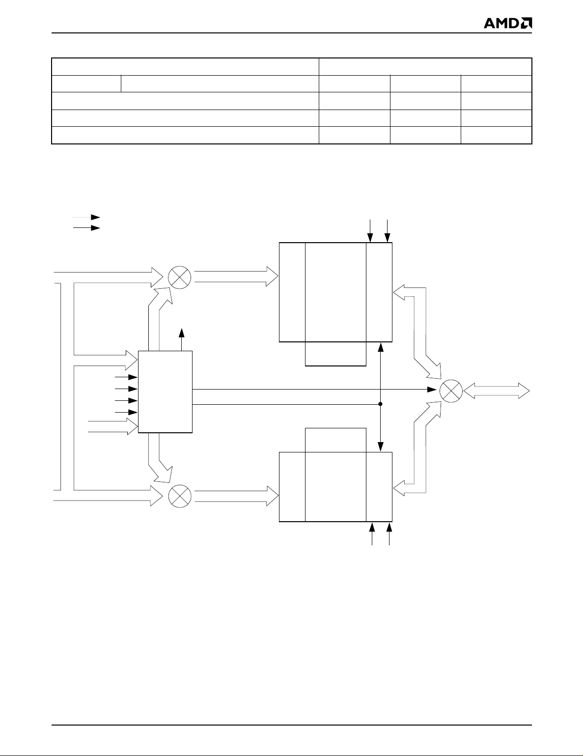
Simultaneous Read/Write Operations with Zero Latency
The Simultaneous Read/Write architecture provides simultaneous operation by dividing the memory space
into two banks. Bank 1 contains eight boot/parameter
sectors, and Bank 2 consists of fourteen larger, code
sectors of uniform size. The dev ice can improv e o v erall
system performance by allowing a host system to program or erase in one bank, th en immediately and simultaneously read from the other bank, with zero
latency. This releases the system from waiting for the
completion of program or erase operations.
Am29DL800B Features
The device offers complete compatibility with the
JEDEC single-power-supply Flash command set
standard. Commands are written to the command
register using standard micr oprocessor write timings.
Register contents serve as input to an internal state
machine that controls the erase and programming
circuitry. Write cycles also internally latch addresses
and data needed for the programming and erase
operations. Reading data out of the device is similar to
reading from other Flash or EPROM devices.
Device programming occurs by executing the program
command sequence. This initiates the Embedded
Program algorithm—an internal algorithm that automatically times the program pulse widths and verifies
proper cell margin. The Unlock Bypass mode facili-
tates faster programming time s by requiring only two
write cycles to program data instead of four.
Device erasure occurs by executing the erase command sequenc e. This initiates the Embedded Erase
algorithm—an in ternal algorithm that auto matically
preprograms the arra y (if it is not already progr ammed)
before e xecuting the er ase operation. During erase, the
device automatically times the erase pulse widths and
verifies proper cell margin.
The host system can detect whether a program or
erase operation is complete by observing the RY/BY#
pin, or by reading the DQ7 (Data# Polling) and DQ6
(toggle) status bits. After a program or erase cycl e has
been completed, the device automatically returns to
reading array data.
The sector erase ar chitecture allo ws memo ry secto rs
to be erased and reprogrammed without affecting the
data contents of other sectors. The device is fully
erased when shipped from the factory.
Hardware data protection measures include a low
detector that automatically in hibits write opera-
V
CC
tions during power transitions. The hardware sector
protection feature disables both program and erase
operations in any combination of the sectors of memory. This can be achieved in-system or via programming equipment.
The Erase Suspend feature enables the user to put
erase on hold for any period of time to read data from,
or program data to, any sector within that bank that is
not selected for erasure. Tr ue background erase can
thus be achieved. There is no need to suspend the
erase operation if the read data is in the other bank.
The hardware RESET# pin term inates any operation
in progress and resets the internal state machine to
reading array dat a. The RESET# pin ma y be tied to the
system reset circuitry. A system reset would thus also
reset the device to reading array data, enab ling the system microprocessor to read the boot-up firmware from
the Flash memory.
The device off ers two power-sa ving f eatures. When addresses have been stable for a specified amount of
time, the device enters the automatic sleep m ode.
The system can also place the de vice into the standby
mode. Power consumption is greatly reduced in both
these modes.
AMD’s Flash technology combines years of Flash memory manufacturin g experience to produce th e highest
levels of quality, reliability, and cost effectiveness. The
device electrically erases all bits within a sector simultaneously via Fowler-Nordheim tunneling. The bytes are
programmed one byte or word at a time using hot electron injection.
2 Am29DL800B
PRELIMINARY
PRODUCT SELECTOR GUIDE
Family Part Number Am29DL800B
Speed Option Full Voltage Range: V
= 2.7 – 3.6 V 70 90 120
CC
Max Access Time (ns) 70 90 120
CE# Access (ns) 70 90 120
OE# Access (ns) 30 35 50
Note: See “AC Characteristics” for full specifications.
BLOCK DIAGRAM
V
CC
V
SS
A0–A18
A0–A18
RESET#
WE#
CE#
BYTE#
DQ0–DQ15
RY/BY#
A0–A18A0–A18
STATE
CONTROL
&
COMMAND
REGISTER
Upper Bank Address
Upper Bank
Y-Decoder
X-Decoder
Status
Control
X-Decoder
OE# BYTE#
Latches and Control Logic
DQ0–DQ15
A0–A18
Lower Bank Address
DQ0–DQ15 DQ0–DQ15
Lower Bank
Y-Decoder
Latches and
Control Logic
OE# BYTE#
21519A-1
Am29DL800B 3
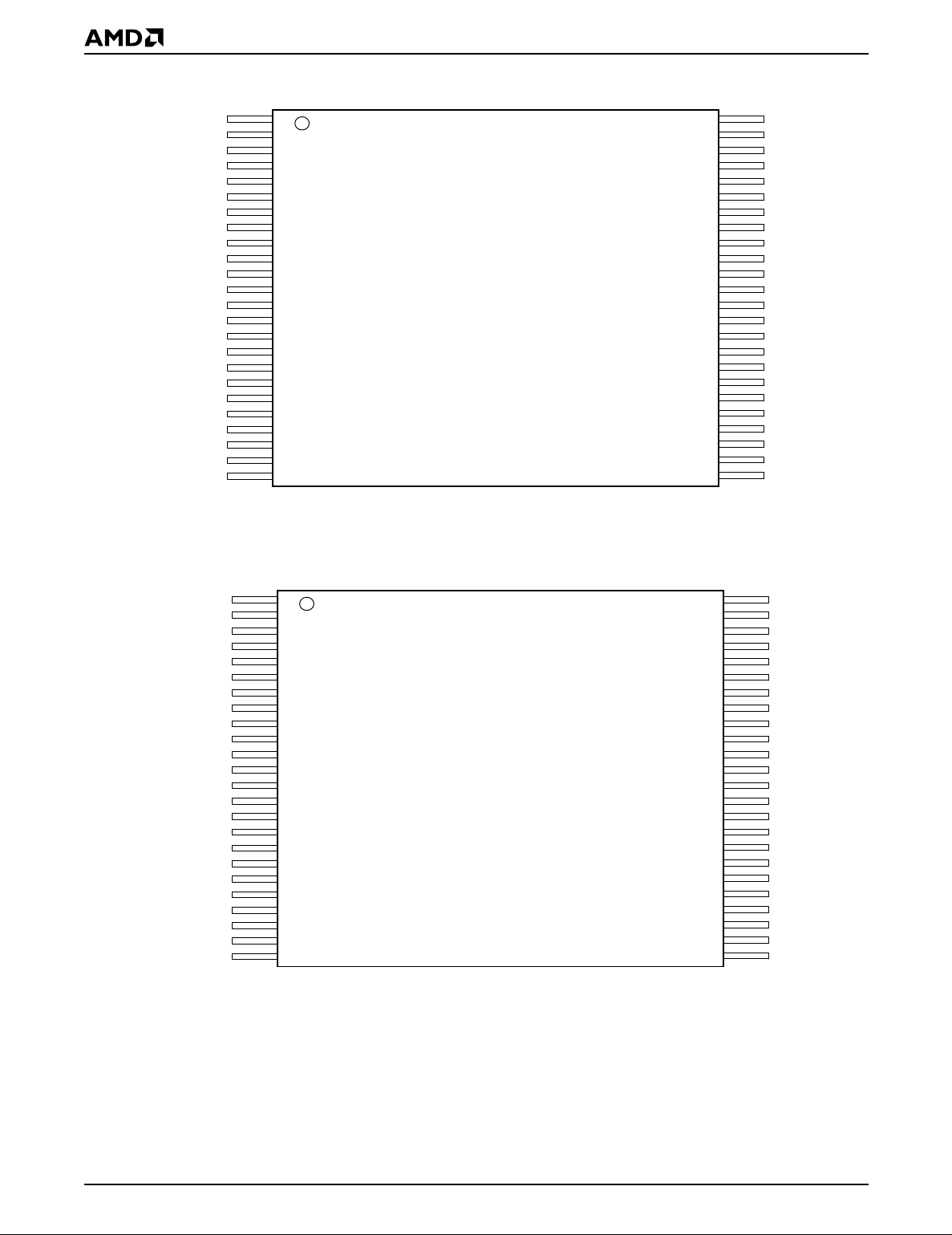
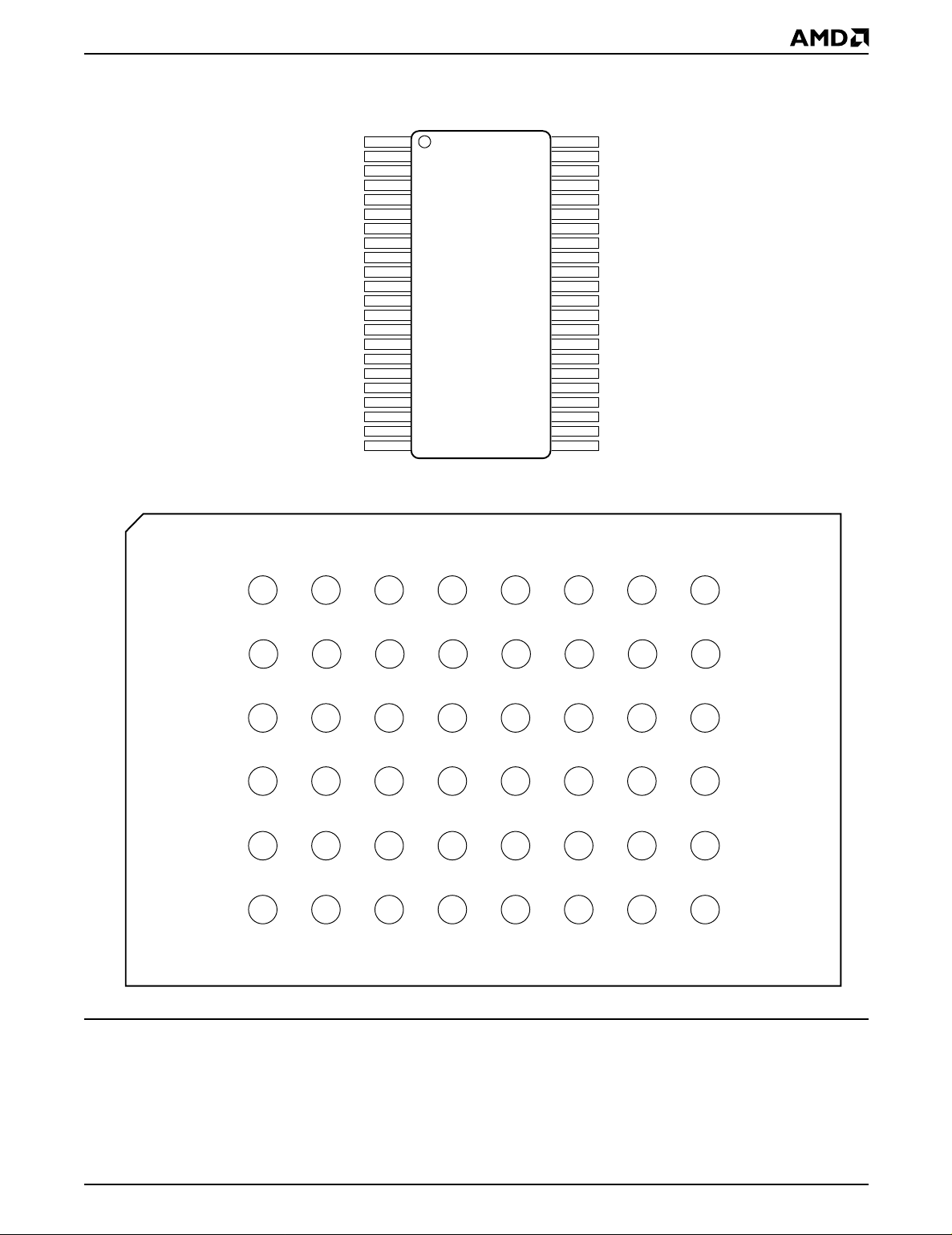
CONNECTION DIAGRAMS
PRELIMINARY
A15
A14
A13
A12
A11
A10
A9
A8
NC
NC
WE#
RESET#
NC
NC
RY/BY#
A18
A17
A7
A6
A5
A4
A3
A2
A1
1
2
3
4
5
6
7
8
9
10
11
12
13
14
15
16
17
18
19
20
21
22
23
24
Standard TSOP
48
47
46
45
44
43
42
41
40
39
38
37
36
35
34
33
32
31
30
29
28
27
26
25
A16
BYTE#
V
SS
DQ15/A-1
DQ7
DQ14
DQ6
DQ13
DQ5
DQ12
DQ4
V
CC
DQ11
DQ3
DQ10
DQ2
DQ9
DQ1
DQ8
DQ0
OE#
V
SS
CE#
A0
A16
BYTE#
V
SS
DQ15/A-1
DQ7
DQ14
DQ6
DQ13
DQ5
DQ12
DQ4
V
CC
DQ11
DQ3
DQ10
DQ2
DQ9
DQ1
DQ8
DQ0
OE#
V
SS
CE#
A0
1
2
3
4
5
6
7
8
9
10
11
12
13
14
15
16
17
18
19
20
21
22
23
24
Reverse TSOP
48
47
46
45
44
43
42
41
40
39
38
37
36
35
34
33
32
31
30
29
28
27
26
25
A15
A14
A13
A12
A11
A10
A9
A8
NC
NC
WE#
RESET#
NC
NC
RY/BY#
A18
A17
A7
A6
A5
A4
A3
A2
A1
21519A-2
4 Am29DL800B
CONNECTION DIAGRAMS
PRELIMINARY
RY/BY#
A18
A17
A7
A6
A5
A4
A3
A2
A1
A0
CE#
V
SS
OE#
DQ0
DQ8
DQ1
DQ9
DQ2
DQ10
DQ3
DQ11
10
11
12
13
14
15
16
17
18
19
20
21
22
1
2
3
4
5
6
7
8
9
SO
44
43
42
41
40
39
38
37
36
35
34
33
32
31
30
29
28
27
26
25
24
23
RESET#
WE#
A8
A9
A10
A11
A12
A13
A14
A15
A16
BYTE#
V
SS
DQ15/A-1
DQ7
DQ14
DQ6
DQ13
DQ5
DQ12
DQ4
V
CC
FBGA
Bump Side (Bottom) View
A1 B1 C1 D1 E1 F1 G1 H1
21519A-3
A2 B2 C2 D2 E2 F2 G2 H2
A3 B3 C3 D3 E3 F3 G3 H3
A4 B4 C4 D4 E4 F4 G4 H4
A5 B5 C5 D5 E5 F5 G5 H5
A6 B6 C6 D6 E6 F6 G6 H6
Special Handling Instructions for FBGA Package
Special handling is required for Flash Memory products
in FBGA packages.
CE#A0A1A2A4A3
OE# V
SS
DQ9 DQ1DQ8DQ0A5A6A17A7
DQ11 DQ3DQ10DQ2NCA18NCRY/BY#
V
CC
DQ4DQ12DQ5NCNCRESET#WE#
DQ13 DQ6DQ14DQ7A11A10A8A9
BYTE#A16A15A14A12A13
DQ15/A-1 V
SS
Flash memory devices in FBGA packages may be
damaged if exposed to ultrasonic cleaning methods.
The package and/or data integrity may be
compromised if the package bod y is exposed to
temperatures above 150°C for prolonged periods of
time.
Am29DL800B 5
PRELIMINARY
PIN DESCRIPTION
A0-A18 = 19 Addresses
DQ0-DQ14= 15 Data Inputs/Outputs
DQ15/A-1 = DQ15 (Data Input/Output, word mode),
A-1 (LSB Address Input, byte mode)
CE# = Chip Enable
OE# = Output En able
WE# = Write Enable
BYTE# = Selects 8-bit or 16-bit mode
RESET# = Hardware Reset Pin, Active Low
RY/BY# = Ready/Busy Output
= 3.0 volt-only single power supply
V
CC
V
SS
NC = Pin Not Connected Internally
(see Product Selector Guide for speed
options and voltage supply tolerances)
= Device Ground
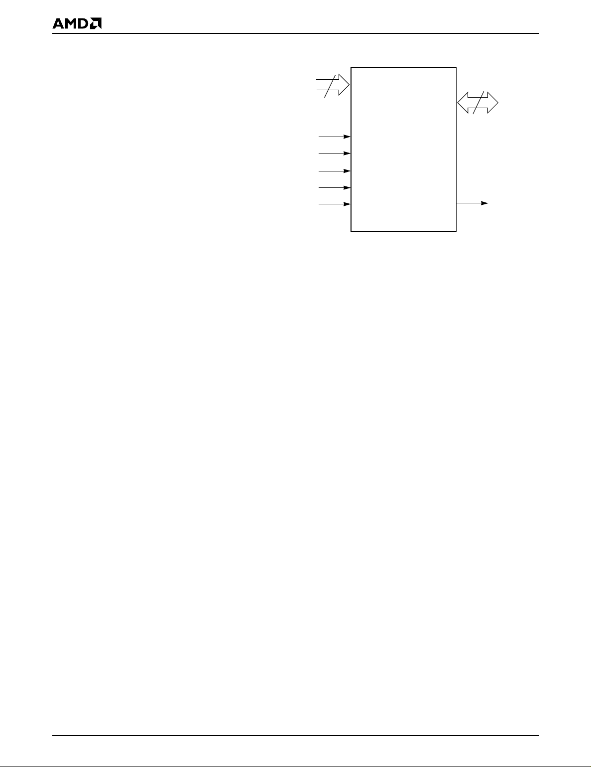
LOGIC SYMBOL
19
A0–A18
CE#
OE#
WE#
RESET#
BYTE# RY/BY#
16 or 8
DQ0–DQ15
(A-1)
21519A-4
6 Am29DL800B
PRELIMINARY
ORDERING INFORMATION
Standard Pr od ucts
AMD standard products are available in several packages and operating ranges. The order number (Valid Combination) is
formed by a combination of the following:
Am29DL800B 70 E C
T
DEVICE NUMBER/DES CR IPT IO N
Am29DL800B
8 Megabit (1 M x 8-Bit/512 K x 16-Bit) CMOS Flash Memory
3.0 Volt-only Read, Program, and Erase
OPTIONAL PROCESSING
Blank = Standa rd Pro ces sin g
B = Burn-in
(Contact an AMD representative for more information)
TEMPERATURE RANGE
C=Commercial (0°C to +70°C)
I = Industrial (–40°C to +85°C)
E = Extended (–55°C to +125°C)
PACKAGE TYPE
E = 40-Pin Thin Small Outline Package (TSOP)
Standard Pinout (TS 040)
F = 40-Pin Thin Small Outline Package (TSOP)
Reverse Pinout (TSR040)
S = 44-Pin Small Outline Package (SO 044)
WB = 48-Ball Fine-Pitch Ball Grid Array (FBGA)
0.80 mm pitch, 6 x 9 mm package
SPEED OPTION
See Product Selector Guide and Valid Combinations
BOOT CODE SECTOR ARCHITECTURE
T = Top Sector
B = Bottom Sector
Am29DL800BT70
Am29DL800BB70
Am29DL800BT90
Am29DL800BB90
Am29DL800BT120
Am29DL800BB120
Valid Combinations
EC, EI, FC, FI,
SC, SI, WBC, WBI
EC, EI, EE,
FC, FI, FE,
SC, SI, SE,
WBC, WBI, WBE
Valid Combinations
Valid Combinations list configurations planned to be supported in volume for this device. Consult the local AMD sales
office to confirm availability of specific valid combinations and
to check on newly released combinations.
Am29DL800B 7
PRELIMINARY
DEVICE BUS OPERATIONS
This section describes the requirements and use of the
device bus operations, which are initiated through the
internal c ommand register. The command register itself does not occupy any addressable memory location. The register is a latch used to store the
commands, along with the address and data information needed to execute the command. The contents of
Table 1. Am29DL800B Device Bus Operations
Operation CE# OE # WE# R ESET#
Read L L H H A
Write L H L H A
Standby
Output Disable L H H H X High-Z High-Z High-Z
Reset X X X L X High-Z High-Z High-Z
Sector Protect (Note 2) L H L V
Sector Unprotect (Note 2) L H L V
Temporary Sector Unprotect X X X V
Legend:
L = Logic Low = V
Notes:
1. Addresses are A18:A0 in word mode (BYTE# = V
2. The sector protect and sector unprotect functions may also be implemented via programming equipment. See the “Sector
Protection/Unprotection” section.
, H = Logic High = VIH, VID = 12.0 ± 0.5 V, X = Don’t Care, AIN = Address In, DIN = Data In, D
IL
VCC ±
0.3 V
XX
VCC ±
0.3 V
), A18:A-1 in byte mode (BYTE# = VIL).
IH
the register serve as inputs to the internal state machine. The state machine outputs dictate the function of
the device. Table 1 lists the device bus operations, the
inputs and control lev els t he y requ ire , and t he resulting
output. The following subsections describe each of
these operations in further detail.
DQ8–DQ15
Sector Address,
A6 = L, A1 = H,
ID
Sector Address,
A6 = H, A1 = H,
ID
ID
Addresses
(Note 1)
IN
IN
X High-Z High-Z High-Z
A0 = L
A0 = L
A
IN
DQ0–
DQ7
D
OUT
D
IN
D
IN
D
IN
D
IN
BYTE#
= V
IH
D
DQ8–DQ14 = High-Z,
OUT
D
IN
XX
XX
D
IN
DQ15 = A-1
BYTE#
= V
IL
High-Z
= Data Out
OUT
Word/Byte Configuration
The BYTE# pin controls whether the device data I/O
pins operate in the byte or word configuration. If the
BYTE# pin is set at logic ‘1’, the device is in word con-
figuration, DQ0-15 are active and controlled by CE#
and OE# .
If the BYTE# pin is set at logic ‘0’, the device is in byte
configuration, and only data I/O pins DQ0–DQ7 are active and controlled by CE# and OE#. The data I/O pins
DQ8–DQ14 are tri-stated, and the DQ15 pin is used as
an input for the LSB (A-1) address function.
Requirements for Reading Array Data
To read array data from the outputs, the system must
drive the CE# and OE# pins to V
control and selects the device. OE# is the output control and gates arra y data to the output pins . WE# should
remain at V
. The BYTE# pin determines whether the
IH
device outputs array data in words or bytes.
. CE# is the power
IL
The internal state machine is set for reading array
data upon device po wer-u p , or after a hardw are res et.
This ensure s that no sp urious alteration of the memory content occurs dur ing the power transition. No
command is nece ssary in this mode to ob tain array
data. Standard microprocessor read cycles that assert valid addresses on the de vice addr ess inputs produce valid d ata on the de vice da ta outputs . EAch bank
remains enabled for read access until the command
register contents are altered.
See “Reading Array Data” for more information. Refer
to the AC Read-Only Operations table for timing specifications and to Figure 13 for the timing diagram. I
in the DC Characteristics table represents the active
current specification for reading array data.
Writing Commands/Command Sequences
To wr ite a command or command sequence (which includes programming data to the device and erasing
8 Am29DL800B
CC1

PRELIMINARY
sectors of memory), the system must drive WE# and
CE# to V
, and OE# to VIH.
IL
For progr am operations , the BYTE# pin determines whether
the device accept s progr am data in by tes or words . Ref er to
“Word/Byte Confi gurat ion” f or more inf ormation.
The device features an Unlock Bypass mode to facili-
tate faster programming. Once a bank enters the Unlock
Bypass mode, only two write cycles are required to program a word or byte, instead of four. The “Byte/Word
Program Command Sequence” section has details on
programming data to the device using both standard and
Unlock Bypass command sequences.
An erase operation can erase one sect or, multiple sectors, or the entire device. Tables 2 and 3 indicate the
address space that each sector occupies. The device
address space is divided into two banks: Bank 1 contains the boot/parameter sectors, and Bank 2 contains
the larger, code sectors of uniform size. A “bank address” is the address bits required to uniquely select a
bank. Similarly, a “sector address” is the address bits
required to uniquely select a sector.
If the system writes the autoselect co mmand sequence, the device enters the autoselect mode. The
system can then read autoselect codes from the internal register (which is separate from the memory array)
on DQ7–DQ0. Standard read cycle timings apply in this
mode. Refer to the Autoselect Mode and Autoselect
Command Sequence sections for more information.
in the DC Characteristics table represents the ac-
I
CC2
tive current specification for the write mode. The AC
Characteristics section contains timing specification tables and timing diagrams for write operations.
Simultaneous Read/Write Operations with Zero Latency
This device is capable of readin g data from one bank of
memory while programming or erasing in the other
bank of memory. An erase operation may also be suspended to read from or pro gram to another location
within the same bank (except t he sector b eing erased).
Figure 19 shows how read and write cycles may be initiated for simultaneous operation with zero latency.
I
CC6
and I
in the DC Characteristics table represent
CC7
the current specificatio ns for read-while-program and
read-while-erase, respectively.
Standby Mode
When the system is not reading or writing to the device ,
it can place the device in the standby mode. In this
mode, current consumption is gr eatly reduced, and the
outputs are placed in the high impedance state, independent of the OE# input.
The device enters the CMOS standby mode when the
CE# and RESET# pins are both held at V
CC
± 0.3 V.
(Note that this is a more restricted voltage range than
.) If CE# and RESET# ar e held at VIH, but not within
V
IH
± 0.3 V, the device will be in the standby mode, b ut
V
CC
the standby current will be grea ter. The de vice requires
standard access time (t
) for read access when the
CE
device is in either of these standby modes, before it is
ready to read data.
If the device is deselected during erasure or programming, the device draws active current until the
operation is completed.
in the DC Characteristics table represents the
I
CC3
standby current specification.
Automatic Sleep Mode
The automatic sleep mode minimizes Flash device
energy consumption. The de vice automatically enables
this mode when addresses remain stable f or t
ns. The automatic sleep mode is independent of the
CE#, WE#, and OE# control signals. Standard addres s
access timings provide new data when addresses are
changed. While in sleep mode, output data is latched
and always available to the system. I
CC4
Characteristics table represents the automatic sleep
mode current specification.
+ 30
ACC
in the DC
Am29DL800B 9

PRELIMINARY
RESET#: Hardware Reset Pin
The RESET# pin provides a har dware method of resetting the device to reading array data. When the RESET# pin is driven low for at least a period of t
device immediately terminates any operation in
progress, tristates all output pins, and ignores all read/
write commands for the duration of the RESET# pulse .
The device also resets the internal state machine to
reading array data. The operation that was interrupted
should be reinitiated once the de vi ce is ready to accept
another command sequence, to ensure data integrity.
Current is reduced for the duration of the RESET#
pulse. When RESET# is held at V
draws CMOS standby current (I
but not within VSS±0.3 V, the standby current will
at V
IL
±0.3 V, the device
SS
). If RESET# is held
CC4
be greater.
The RESET# pin may be tied to the system reset cir-
cuitry. A system reset would thus also reset the Flash
RP
, the
memory, enabling the system to read the boot-up
firmware from the Flash memory.
If RESET# is asserted during a program or erase operation, the RY/BY# pin remains a “0” (busy) until the internal reset operatio n is complete, which requires a
time of t
(during Embedded Algorithms). The
READY
system can thus monitor RY/BY# to determine whether
the reset operation is complete. If RESET# is asserted
when a program or erase operation is not executing
(RY/BY# pin is “1”), the reset operation is completed
within a time of t
rithms). The system can read data t
SET# pin returns to V
(not during Embe dded Algo-
READY
.
IH
RH
after the RE-
Refer to the AC Characteristics tables for RESET# parameters and to Figure 14 for the timing diagram.
Output Disable Mode
When the OE# input is at VIH, output from the device is
disabled. The output pins are placed in t he high impedance state.
10 Am29DL800B
PRELIMINARY
Bank Sector
SA0 0 0 0 0 X X X 64/32 00000h–0FFFFh 00000h–07FFFh
SA1 0 0 0 1 X X X 64/32 10000h–1FFFFh 08000h–0FFFFh
SA2 0 0 1 0 X X X 64/32 20000h–2FFFFh 10000h–17FFFh
SA3 0 0 1 1 X X X 64/32 30000h–3FFFFh 18000h–1FFFFh
SA4 0 1 0 0 X X X 64/32 40000h–4FFFFh 20000h–27FFFh
SA5 0 1 0 1 X X X 64/32 50000h–5FFFFh 28000h–2FFFFh
SA6 0 1 1 0 X X X 64/32 60000h–6FFFFh 30000h–37FFFh
Bank 2
SA7 0 1 1 1 X X X 64/32 70000h–7FFFFh 38000h–3FFFFh
SA8 1 0 0 0 X X X 64/32 80000h–8FFFFh 40000h–47FFFh
SA9 1 0 0 1 X X X 64/32 90000h–9FFFFh 48000h–4FFFFh
SA10 1 0 1 0 X X X 64/32 A0000h–AFFFFh 50000h–57FFFh
SA11 1 0 1 1 X X X 64/32 B0000h–BFFFFh 58000h–5FFFFh
SA12 1 1 0 0 X X X 64/32 C0000h–CFFFFh 60000h–67FFFh
Table 2.
Sector Address
Bank Address
Am29DL800BT Top Boot Sector Architecture
Sector Size
(Kbytes/
A15 A14 A13 A12A18 A17 A16
Kwords)
(x8)
Address Range
(x16)
Address Range
SA13 1 1 0 1 X X X 64/32 D0000h–DFFFFh 68000h–6FFFFh
SA14 1 1 1 0 0 0 X 16/8 E0000h–E3FFFh 70000h–71FFFh
Bank 1
SA151110
SA16 1 1 1 0 1 1 0 8/4 EC000h–EDFFFh 76000h–76FFFh
SA17 1 1 1 0 1 1 1 8/4 EE000h–EFFFFh 77000h–77FFFh
SA18 1 1 1 1 0 0 0 8/4 F0000h–F1FFFh 78000h–78FFFh
SA19 1 1 1 1 0 0 1 8/4 F2000h–F3FFFh 79000h–79FFFh
SA201111
SA21 1 1 1 1 1 1 X 16/8 FC000h–FFFFFh 7E000h–7FFFFh
01X
32/16
10X
01X
32/16
10X
E4000h–E7FFFh,
E8000h–EBFFFh
F4000h–F7FFFh,
F8000h–FBFFFh
72000h–73FFFh
74000h–75FFFh
7A000h–7BFFFh
7C000h–7DFFFh
Note: The address range is A18:A-1 if in byte mode (BYTE# = VIL). The address range is A18:A0 if in word mode (BYTE# = VIH).
Am29DL800B 11
Bank Sector
SA211111XXX 64/32 F0000h–FFFFFh 78000h–7FFFFh
SA20 1 1 1 0 X X X 64/32 E0000h–EFFFFh 70000h–77FFFh
SA19 1 1 0 1 X X X 64/32 D0000h–DFFFFh 68000h–6FFFFh
SA18 1 1 0 0 X X X 64/32 C0000h–CFFFFh 60000h–67FFFh
SA17 1 0 1 1 X X X 64/32 B0000h–BFFFFh 58000h–5FFFFh
SA16 1 0 1 0 X X X 64/32 A0000h–AFFFFh 50000h–57FFFh
Tab le 3. Am29DL800BB Bottom Boot Sector Architecture
Sector Address
Bank Address
PRELIMINARY
A15 A14 A13 A12A18 A17 A16
Sector Size
(Kbytes/
Kwords)
(x8)
Address Range
(x16)
Address Range
Bank 2
Bank 1
SA15 1 0 0 1 X X X 64/32 90000h–9FFFFh 48000h–4FFFFh
SA14 1 0 0 0 X X X 64/32 80000h–8FFFFh 40000h–47FFFh
SA13 0 1 1 1 X X X 64/32 70000h–7FFFFh 38000h–3FFFFh
SA12 0 1 1 0 X X X 64/32 60000h–6FFFFh 30000h–37FFFh
SA11 0 1 0 1 X X X 64/32 50000h–5FFFFh 28000h–2FFFFh
SA10 0 1 0 0 X X X 64/32 40000h–4FFFFh 20000h–27FFFh
SA9 0 0 1 1 X X X 64/32 30000h–3FFFFh 18000h–1FFFFh
SA8 0 0 1 0 X X X 64/32 20000h–2FFFFh 10000h–17FFFh
SA7 0 0 0 1 1 1 X 16/8 1C000h–1FFFFh 0E000h–0FFFFh
SA6 0 0 0 1
SA5 0 0 0 1 0 0 1 8/4 12000h–13FFFh 09000h–09FFFh
SA4 0 0 0 1 0 0 0 8/4 10000h–11FFFh 08000h–08FFFh
SA3 0 0 0 0 1 1 1 8/4 0E000h–0FFFFh 07000h–07FFFh
SA2 0 0 0 0 1 1 0 8/4 0C000h–0DFFFh 06000h–06FFFh
SA1 0 0 0 0
10X
32/16
01X
10X
32/16
01X
18000h–1BFFFh
14000h–17FFFh
08000h–0BFFFh,
04000h–07FFFh
0C000h–0DFFFh
0A000h–0BFFFh
04000h–05FFFh,
02000h–03FFFh,
SA0 0 0 0 0 0 0 X 16/8 00000h–03FFFh 00000h–01FFFh
Note: The address range is A18:A-1 if in byte mode (BYTE# = VIL). The address range is A18:A0 if in word mode (BYTE# = VIH).
Autoselect Mode
The autoselect mode provides manufacturer and device identification, and sector protection verification,
through identifier codes output on DQ7–DQ0. This
mode is primarily intended for progr amming equipment
to automatically match a device to be progr ammed with
its correspondi ng programming al gorithm. However,
the autoselect codes can also be accessed in-system
through the command register.
When using programming equipment, the autoselect
mode requires V
(11.5 V to 12.5 V) on address pin
ID
the sector address must appear on the appropriate
highest order address bits (see Tables 2 and 3). Table
4 shows the remaining address bits that are don’t care .
When all necessary bits have been set as required, the
programming equipment may then read the corresponding identifier code on DQ7-DQ0.
To access the autoselect codes in-system, the host
system can issue the autoselect command via the
command register, as shown in Table 5. This method
does not require V
. Refer to the Autoselect Command
ID
Sequence section for more information.
A9. Address pins A6, A1, and A0 must be as shown in
Ta ble 4. In addition, when verifying sector protection,
12 Am29DL800B
PRELIMINARY
Table 4. Am29DL800B Autoselect Codes (High V o ltage Method)
Description Mode CE# OE# WE#
A18
to
A12
A11
to
A10 A9
A8
to
A7 A6
A5
to
A2 A1 A0
DQ8
to
DQ15
DQ7
to
DQ0
Manufacturer ID: AMD L L H BA X V
Device ID:
Am29DL800B
(Top Boot Block)
Device ID:
Am29DL800B
(Bottom Boot Block)
Sector Protection Verification L L H SA X V
Note: L = Logic Low = VIL, H = Logic High = VIH, BA = Bank Address, SA = Sector Address, X = Don’t care.
Word L L H
BA X V
Byte L L H X 4Ah
Word L L H
BA X V
Byte L L H X CBh
Sector Protection/Unprotection
The hardware sector protection feature disables both
program and erase operations in any sect or. The hardware sector unprotection feature re-enables both program and erase operations in previously protected
sectors. Sector protection/unprotecti on can be implemented via two methods.
The primary method requires V
on the RESET# pin
ID
XLXLL X 01h
ID
22h 4Ah
XLXLH
ID
22h CBh
XLXLH
ID
XLXHL
ID
SET# pin to V
(11.5 V – 12.5 V). During this mode,
ID
formerly protected sectors can be programmed or
erased by selecting the sector addresses. Once V
removed from the RESET# pin, all the previously protected sectors are protected again. Figure 1 shows the
algorithm, and Figur e 23 shows the timing diagrams,
for this feature.
only, and can be implemented either in-system or via
programming equipment. Figure 2 shows the algorithms and Figure 24 shows the timing diagram. This
START
method uses standard m icroprocessor bus cycle timing. For sector unprotect, all unprotected sectors must
first be protected prior to the first sector unpro tect write
cycle.
RESET# = V
(Note 1)
ID
X
X
01h
(protected)
00h
(unprotected)
ID
is
The alternate method intended on ly for programming
equipment requires V
on address pin A9 and OE#.
ID
This method is compatible with programmer routines
written for earlier 3.0 v olt-only AMD flash de vices. Publication number 21467 contains further details; contact
an AMD representative to request a copy.
The device is shipped with all sectors unprotected.
AMD offers the option of programming and protecting
sectors at its factory prior to shipping the device
through AMD’s ExpressFlash™ Servic e. Contact an
AMD representative for details.
It is possible to determine whether a sector is protected
or unprotected. See the Autoselect Mode section for
details.
Temporary Sector Unprotect
This feature allows temporary unpr otection of previously protected sectors to change data in-system. The
Sector Unprotect mode is activated by setting the RE-
Am29DL800B 13
Perform Erase or
Program Operations
RESET# = V
Temporary Sector
Unprotect Completed
(Note 2)
Notes:
1. All protected sectors unprotected.
2. All previously protected sectors are protected once
again.
IH
21519A-5
Figure 1. Temporary Sector Unprotect Operation
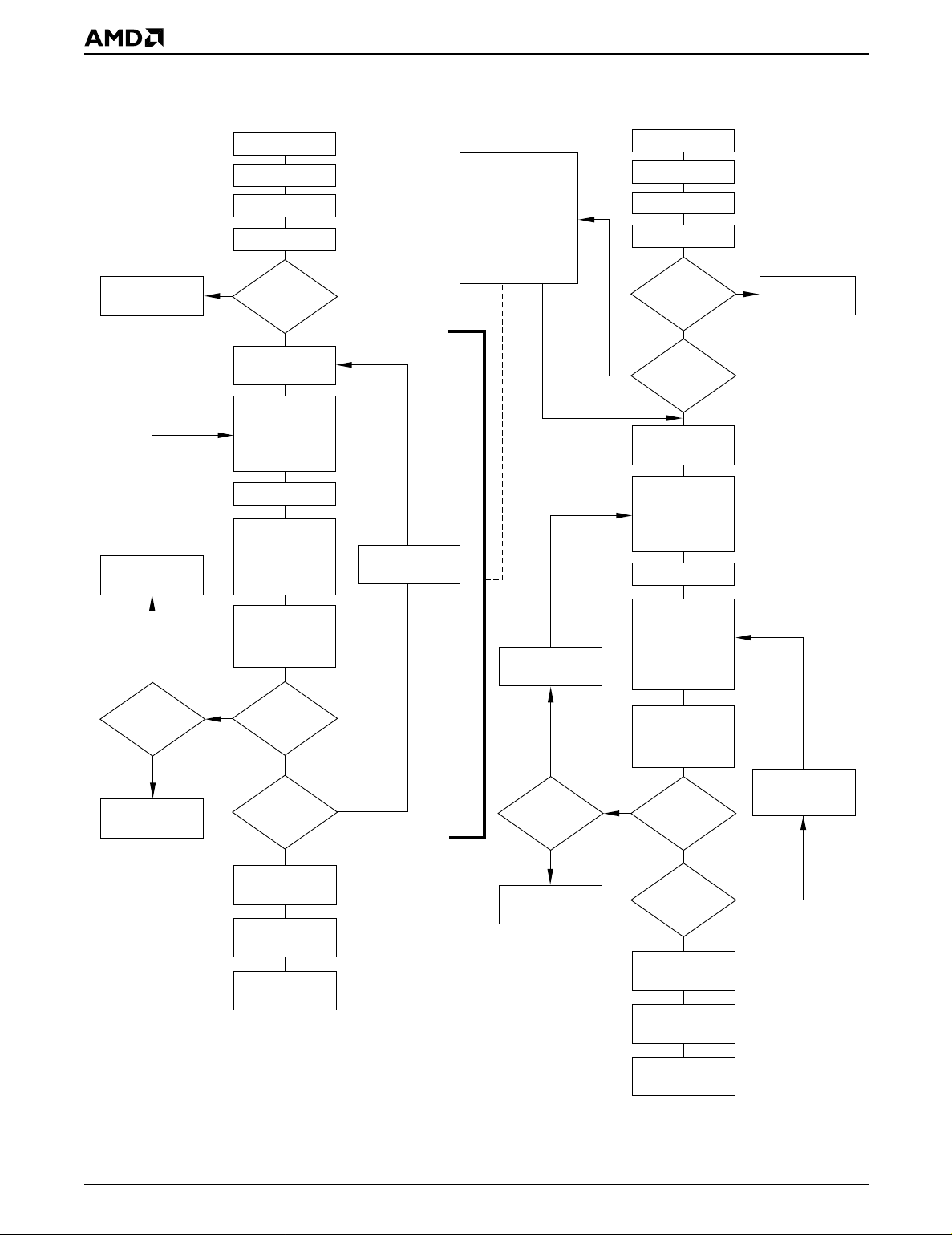
PRELIMINARY
Temporary Sector
Unprotect Mode
Increment
PLSCNT
No
PLSCNT
= 25?
Yes
Device failed
Sector Protect
Algorithm
START
PLSCNT = 1
RESET# = V
Wait 1 µs
No
First Write
Cycle = 60h?
Set up sector
address
Sector Protect:
Write 60h to sector
address with
A6 = 0, A1 = 1,
A0 = 0
Wait 150 µs
Verify Sector
Protect: Write 40h
to sector address
with A6 = 0,
A1 = 1, A0 = 0
Read from
sector address
with A6 = 0,
A1 = 1, A0 = 0
No
Data = 01h?
Protect another
sector?
Remove V
from RESET#
Write reset
command
Sector Protect
complete
Yes
Yes
No
START
Protect all sectors:
The indicated portion
of the sector protect
ID
Reset
PLSCNT = 1
Yes
ID
algorithm must be
performed for all
unprotected sectors
prior to issuing the
first sector
unprotect address
Increment
PLSCNT
No
PLSCNT
= 1000?
Yes
Device failed
Sector Unprotect
PLSCNT = 1
RESET# = V
Wait 1 µs
First Write
Cycle = 60h?
No
All sectors
protected?
Set up first sector
address
Sector Unprotect:
Write 60h to sector
address with
A6 = 1, A1 = 1,
A0 = 0
Wait 15 ms
Verify Sector
Unprotect: Write
40h to sector
address with
A6 = 1, A1 = 1,
A0 = 0
Read from
sector address
with A6 = 1,
A1 = 1, A0 = 0
No
Data = 00h?
Last sector
verified?
Remove V
from RESET#
Yes
Yes
Yes
Yes
ID
No
Temporary Sector
Unprotect Mode
Set up
next sector
address
No
ID
Algorithm
Write reset
command
Figure 2. In-System Sector Protect/Unprotect Algorithms
14 Am29DL800B
Sector Unprotect
complete
21519A-6

PRELIMINARY
Hardware Data Protection
The command sequence requirement of unlock cycles
for programming or erasing provides data protection
against inadvertent wri tes (refer to Table 5 for command definitions). In additio n, the following hardware
data protection mea sures prevent accidental erasure
or programming, which might otherwise be caused by
spurious system level signals during V
power-up and
CC
power-down transitions, or from system noise.
Low V
When VCC is less than V
any write cycles. This protects data during V
Write Inhibit
CC
, the device does not accept
LKO
CC
power-up and power-down. The command register and
all internal program/erase circuits are disabled, and the
device resets to reading array data. Subsequent writes
are ignored until V
is greater than V
CC
. The system
LKO
must provide the proper signals to the con trol pins to
COMMAND DEFINITIONS
Writing specific addre ss and data commands or sequences into the command register initiates device operations. Table 5 defines the valid registe r command
sequences. Writing incorrect address and data val-
ues or writing them in the improper sequence resets
the device to reading array data.
All addresses are latched on the falling edge of WE# or
CE#, whichever happens later. All data is latched on
the rising edge of WE# or CE#, whichever happens
first. Refer to the appropriate ti ming diagrams in the A C
Characteristics section.
Reading Array Data
The device is automatically set to reading array data
after device power-up. No commands are required to
retrieve data. Each bank is ready to read array data
after completing an Embedded Program or Embedded
Erase algorithm.
After the device accepts an Er ase Suspend command,
the corresponding bank enters the erase-suspendread mode, after which the system can read data from
any non-erase-suspended sector within the same
bank. After completing a programming operat ion in the
Erase Suspend mode, the system may once again
read array data with the s ame exception. See the Er ase
Suspend/Erase Resume Commands section for more
information.
must
The system
bank to the read (or erase-s uspend-read) mode if DQ5
goes high during an active program or erase operat ion,
or if the bank is in the autoselect mode. See the next
section, Reset Command, for more information.
See also Requirements for Reading Array Data in the
Device Bus Operations section for more information.
issue the reset command to return a
prevent unintentional writes when V
.
V
LKO
is greate r than
CC
Write Pulse “Glitch” Protection
Noise pulses of less than 5 ns (typical) on OE#, CE# or
WE# do not initiate a write cycle.
Logical Inhibit
Write cycles are inhibited by holding any one of OE# =
, CE# = VIH or WE# = VIH. To initiate a write cycle,
V
IL
CE# and WE# must be a logical zero while OE# is a
logical one.
Power-Up Write Inhibit
If WE# = CE# = V
and OE# = VIH during power up , the
IL
device does not accept commands on the rising edge
of WE#. The internal state mac hine is automatically
reset to reading array data on power-up.
The Read-Only Operations table provides the read parameters, and Figure 13 shows the timing diagram.
Reset Command
Writing the reset command resets the banks to the
read or erase-suspend-read mode. Address bits are
don’t cares for this command.
The reset command may be written between the se-
quence cycles in an erase command sequence before
erasing begins. This resets the bank to which the system was writing to reading array data. Once erasure
begins, however, the device ignores reset commands
until the operation is complete.
The reset command may be written between the sequence cycles in a program command sequence before programming begins. This resets the bank to
which the system was writing to the reading array data.
If the program command sequence is written to a bank
that is in the Erase Suspend mode, writing the reset
command returns that bank to the erase-suspend-read
mode. Once programming begins, however, the device
ignores reset commands unti l the operation is complete.
The reset command may be written between the sequence cycles in an autoselect command sequence.
Once in the autoselect mode, t he reset c ommand must
be written to return to reading array data. If a bank entered the autoselect mode while in the Erase Suspend
mode, writing the reset command returns that bank to
the erase-suspend-read mode.
If DQ5 goes high during a program or erase operation,
writing the reset command returns the banks to reading
array data (or erase-suspend-read mode if that bank
was in Erase Suspend).
Am29DL800B 15

PRELIMINARY
Autoselect Command Sequence
The autoselect command sequence allows the host
system to access the manufacturer and de vic es codes ,
and determine whether or not a sector is protected.
T ab le 5 shows the address and data requirements . This
method is an alternative to that shown in Table 4, which
is intended for PROM programmers and requires V
on address pin A9. The autoselect command sequence
may be written to an address within a bank that is either
in the read or erase-suspend-read mode. The autoselect command may not be written while the device is
actively programming or erasing in the other bank.
The autoselect command sequence is initiated by first
writing two unlock cycles. This is followed by a third
write cycle that contains the bank address and the autoselect command. The addressed bank then enters
the autoselect mode. The system may read at any address within the same bank any number of times without initiating another autoselect command sequence:
■ A read cycle at address (BA)XX00h (where BA is
the bank address) returns the manufacturer code.
■ A read cycle at address (BA)XX01h in word mode
(or (BA)XX02h in byte mode) returns the device
code.
■ A read cycle to an address containing a sector address (SA) within the same bank, and the address
02h on A7–A0 in word mode (or the address 04h on
A6–A-1 in byte mode) returns 01h if the sector is
protected, or 00h if it is unprotected. Refer to Tables
2 and 3 for valid sector addresses.
The system may continue to read array data from the
other bank while a bank is in the autoselect mode. To
exit the autoselect mode, the system must write the
reset command to return both banks to reading array
data. If a bank enters the autoselect mode while erase
suspended, a reset command returns that bank to the
erase-suspend-read mode. A subsequent Erase
Resume command returns the bank to the er ase operation.
ID
Byte/Word Program Command Sequence
The system may program the device by word or byte,
depending on the state of the BYTE# pin. Programming is a four-bus-cycle operation. The program command sequence is initiated by writing two unlock write
cycles, followed by the program set-up command. The
program address and data are written next, which in
turn initiate the Embedded Program algorithm. The
not
system is
ings. The device automatically generates the program
pulses and verifies the programmed cell margin. Table
required to provide further controls or tim-
5 shows the address and da ta requirements for the
byte program command sequence.
When the Embedded Program algorithm is complete,
that bank then returns to reading array data and addresses are no longer latched. The system can determine the status of the program operation b y using DQ7,
DQ6, or RY/BY#. Note that while the Embedded Program operation is in progress, the system can read
data from the non-programming bank. Refer to the
Write Operation Status section for information on these
status bits.
Any commands written to the device during the Embedded Program Algorithm are ignored. Note that a
hardware reset immediately ter minates the program
operation. The program command sequence should be
reinitiated once that bank has returned to reading arra y
data, to ensure data integrity.
Programming is allowed in any sequence an d across
sector boundaries. A bit cannot be programmed
from “0” back to a “1.” Attempting to do so ma y cause
that bank to set DQ5 = 1, or cause the DQ7 and DQ6
status bits to indicate the operation was successful.
However, a succeeding read will show that the data is
still “0.” Only erase operations c an convert a “0” to a
“1.”
Unlock Bypass Command Sequence
The unlock bypass feature allows the system to program bytes or words to a bank faster than using the
standard program command sequence. The unloc k b ypass command sequence is initiated by first writing two
unlock cycles. This is followed by a third write cycle
containing the unlock bypass command, 20h . That
bank then enters the unlock bypass mode. A two-cy cle
unlock bypass program command sequence is all that
is required to program in this mode. The first cycle in
this sequence contains the unlock bypass program
command, A0h; the second cycle contains the prog ram
address and data. Additional data is programmed in
the same manner. This mode dispenses with t he i nitial
two unlock cycles required in the standard program
command sequence, resulting in faster total programming time. Table 5 shows the requirements for the command sequence.
During the unlock bypass mode, only the Unlock Bypass
Program and Unlock Bypass Reset commands are
valid. To exit the unlock bypass mode, the system must
issue the two-cycle unlock bypass reset command sequence. The first cycle must conta in the bank address
and the data 90h. The second cycle need only con tain
the data 00h. The bank the n returns to readin g array
data.
16 Am29DL800B

PRELIMINARY
Figure 3 illustrates the algorithm for the program operation. Refer to the Er ase and Program Operation s table
in the AC Characteristics section for parameters, and
Figure 17 for timing diagrams.
START
Write Program
Command Sequence
Data Poll
Embedded
Program
algorithm
in progress
Increment Address
Note: See Table 5 for program command sequence.
No
from System
Verify Data?
Yes
Last Address?
Yes
Programming
Completed
No
21519A-7
Figure 3. Program Operation
Chip Erase Command Sequence
Chip erase is a six bus cycle oper ation. The chip er ase
command sequence is initiated by writing two unlock
cycles, followed by a set-up command. Two additional
unlock write cycles are then followed by the chip erase
command, which in turn invokes the Embedded Erase
not
algorithm. The device does
preprogram prior to erase. The Embedded Erase algorithm automatically preprograms and ve rifies the entire
memory for an all zero data patter n prior to electr ical
erase. The system is not required to provide any controls or timings during these operations. Table 5 shows
the address and data requirements for the chip erase
command sequence.
When the Embedded Erase algorithm is complete , that
bank returns to reading array data and addresses are
no longer latched. The system can determine the sta-
require the system to
tus of the erase operation b y using DQ7, DQ6, DQ2, or
RY/BY#. Ref er to the Write Operation Stat us section for
information on these status bits.
Any commands written during the chip erase operation
are ignored. However, note that a hardware reset im-
mediately terminates the erase operation. If that occurs, the chip erase command sequence should be
reinitiated once that bank has returned to reading arra y
data, to ensure data integrity.
Figure 4 illustrates the algorithm for the erase operation. Refer to the Erase and Prog ram Oper ations tab les
in the AC Characteristics section for parameters, and
Figure 18 section for timing diagrams.
Sector Erase Command Sequence
Sector erase is a six bus cycle operation. The sector
erase command sequence is initiated by writing two unlock cycles, followed by a set-up command. Two additional unlock cycles are written, and are then followed
by the address of the sector t o be er ased, and t he sector erase command. Table 5 shows the address and
data requirements for the sector erase comma nd sequence.
not
The device does
prior to erase. The Embedded Erase algorithm automatically programs and verifies the entire memory for
an all zero data pattern prior to electrical erase. The
system is not required to provide a ny controls or timings during these operations.
After the command sequence is written, a sector erase
time-out of 50 µs occurs. Duri ng the time-out period,
additional sector addresses and sector erase commands may be written. Loading the sector erase buffer
may be done in any sequence, and the number of sectors may be from one sector to all sector s. The time between these additional cycl es must be less than 50 µs,
otherwise the last address and command may not be
accepted, and erasure may begin. It is recommended
that processor interrupts be disab led during this time to
ensure all commands are accepted. The interrupts can
be re-enabled after the last Sector Erase command is
written. Any command other than Sector Erase or
Erase Suspend during the time-out period resets
that bank to reading array data. The system must re-
write the c ommand sequ ence and any a dditional addresses and commands.
The system can monitor DQ3 (in the erasing bank) to
determine if the sec tor erase timer has timed out (See
the section on DQ3: Sector Erase Timer.). The time-out
begins from the rising edge of the final WE# pulse in the
command sequence.
When the Embedded Erase algorithm is complete, the
bank returns to reading array data and addresses are
no longer latched. Note that while the Embedded Erase
operation is in progress, the system can read data from
require the system to preprogram
Am29DL800B 17

PRELIMINARY
the non-erasing bank. The system can determine the
status of the erase operation by reading DQ7, DQ6,
DQ2, or RY/BY# in the eras ing bank. Ref er to the Write
Operation Status section for information on these status bits.
Once the sector erase operation has begun, onl y the
Erase Suspend command is valid. All other commands
are ignored. However, note that a hardware reset im-
mediately terminates the erase operation. If that occurs, the sector erase command sequence should be
reinitiated once that bank has returned to reading arra y
data, to ensure data integrity.
Figure 4 illustrates the algorithm for the erase operation. Refer to the Erase and Program Operation s tables
in the AC Characteristics section for parameters, and
Figure 18 section for timing diagrams.
Erase Suspend/Erase Resume Commands
The Erase Suspend command, B0h, allows the system to interrupt a sector erase operation and then
read data from, or progr a m dat a to, any sec tor no t s elected for er asure . The bank addres s is required when
writing this command. This command i s valid only during the sector erase operation, including the 50 µs
time-out period during the sector erase command sequence. The Erase Suspend comma nd is ignored if
written during the chip erase operation or Embedded
Program algorithm.
When the Erase Suspend command is written during
the sector erase operation, the device requires a maximum of 20 µs to suspend the erase operation. However, when the Erase Suspend command is written
during the sector erase time-out, the device immediately terminates the time-out period and suspends the
erase operation.
gram operation using the DQ7 or DQ6 status bits, just
as in the standard Byte Program oper ation. Ref er to the
Write Operation Status section for more information.
In the erase-suspend-read mode, the system can also
issue the autoselect command sequence. Refer to the
Autoselect Mode and Autoselect Command Sequence
sections for details.
To resume the sector erase operation, the system must
write the Erase Resume command. The bank address
of the erase-suspended bank is required when writing
this command. Further writes of the Resume command
are ignored. Another Erase Suspend command can be
written after the chip has resumed erasing.
START
Write Erase
Command Sequence
(Notes 1, 2)
Data Poll to Erasing
Bank from System
No
Data = FFh?
Yes
Embedded
Erase
algorithm
in progress
After the erase operation has been suspended, the
bank enters the erase-suspend-read mode. The system can read data from or program data to any sector
not selected for erasure . (The de vice “er ase suspends”
all sectors selected for erasure.) Reading at any address within erase-suspended sectors produces status
information on DQ7–DQ0. The system can use D Q7,
or DQ6 and DQ2 together, to determine if a sector is
actively erasing or is erase-suspended. Refer to the
Notes:
1. See Table 5 for erase command sequence.
2. See the section on DQ3 for information on the sector
Write Operation Status section f or inf ormation on these
status bits.
After an erase-suspended program operation is complete, the bank returns to the erase-suspend-read
mode. The system can determine the status of the pro-
18 Am29DL800B
Erasure Completed
21519A-8
erase timer.
Figure 4. Erase Operation

PRELIMINARY
Table 5. Am29DL800B Command Definitions
Command
Sequence
(Note 1)
Read (Note 6) 1 RA RD
Reset (Note 7) 1 XXX F0
Manufacturer ID
Device ID,
Top Boot Block
Device ID,
Bottom Boot Block
Autoselect (Note 8)
Sector Protect
Verify (Note 9)
Program
Unlock Bypass
Unlock Bypass Program (Note 10) 2 XXX A0 PA PD
Unlock Bypass Reset (Note 11) 2 BA 90 XXX 00
Chip Erase
Sector Erase
Erase Suspend (Note 12) 1 BA B0
Erase Resume (Note 13) 1 BA 30
Word
Byte AAA 555 (BA)AAA
Word
Byte AAA 555 (BA)AAA (BA)X02 4A
Word
Byte AAA 555 (BA)AAA (BA)X02 CB
Word
Byte AAA 555 (BA)AAA
Word
Byte AAA 555 AAA
Word
Byte AAA 555 AAA
Word
Byte AAA 555 AAA AAA 555 AAA
Word
Byte AAA 555 AAA AAA 555
Legend:
X = Don’t care
RA = Address of the memory location to be read.
RD = Data read from location RA during read operation.
PA = Address of the memory location to be programmed.
Addresses latch on the falling edge of the WE# or CE# pulse,
whichever happens later.
First Second Third Fourth Fifth Sixth
Addr Data Addr Data Addr Data Addr Data Addr Data Addr Data
Cycles
555
4
555
4
555
4
555
4
555
4
555
3
555
6
555
6
AA
AA
AA
AA
AA
AA
AA
AA
2AA
2AA
2AA
2AA
2AA
2AA
2AA
2AA
Bus Cycles (Notes 2–5)
(BA)555
55
55
55
55
55
55
55
55
(BA)555
(BA)555
(BA)555
555
555
555
555
90 (BA)X00 01
(BA)X01 224A
90
(BA)X01 22CB
90
(SA)
X02
90
(SA)
X04
A0 PA PD
20
555
80
555
80
XX00
XX01
00
01
AA
AA
2AA
2AA
55
55 SA 30
PD = Data to be programmed at location PA. Data latches on the
rising edge of WE# or CE# pulse, whichever happens first.
SA = Address of the sector to be verified (in autoselect mode) or
erased. Address bits A18–A12 uniquely select any sector.
BA = Address of the bank th at is being switched to autoselect
mode, is in bypass mode, or is being erased. Address bits A18–
A16 select a bank.
555
10
Notes:
1. See Table 1 for description of bus operations.
2. All values are in hexadecimal.
3. Except when reading array or autoselect data, all bus cycles
are write operations.
4. Data bits DQ15–DQ8 are don’t cares for unlock and command
cycles.
5. Address bits A18–A11 are don’t cares for unlock and
command cycles, unless bank address (BA) is required.
6. No unlock or command cycles required when bank is in read
mode.
7. The Reset command is required to return to reading array
data (or to the erase-suspend-read mode if previously in
Erase Suspend) when a bank is in the autoselect mode, or if
DQ5 is goes high (while the bank is providing status
information).
Am29DL800B 19
8. The fourth cycle of the autoselect command sequence is a
read cycle. The system must provide the bank address to
obtain the manufacturer or device ID information.
9. The data is 00h for an unprotected sector and 01h for a
protected sector. See the Autoselect Command Sequence
section for more information.
10. The Unlock Bypass command is required prior to the Unlock
Bypass Program command.
11. The Unlock Bypass Reset command is required to return to
reading array data when the bank is in the un lock bypass
mode.
12. The system may read and program in non-erasing sectors, or
enter the autoselect mode, when in the Erase Suspend mode.
The Erase Suspend command is valid only during a sector
erase operation, and requires the bank address.
13. The Erase Resume command is valid only during the Erase
Suspend mode, and requires the bank address.

PRELIMINARY
WRITE OPERATION STATUS
The device provides several bits to determine the status of a write operation in the bank where a program or
erase operation is in progress: DQ2, DQ3, DQ5, DQ6,
DQ7, and RY/BY#. Table 6 and the following subsections describe the function of these bits . DQ7, RY/BY#,
and DQ6 each offer a method for determining whether
a program or erase operation is complete or in
progress. These three bits are discussed first.
DQ7: Data# Polling
The Data# Polling bit, DQ7, indicates to the host system whether an Embedded Program or Erase algorithm is in progress or completed, or whether a bank is
in Erase Suspend. Data# P olli ng is valid after the rising
edge of the final WE# pulse in the command sequence .
During the Em bedded Program algor ithm, the device
outputs on DQ7 the complement of the datum programmed to DQ7. This DQ7 status also applies to programming during Erase Suspend. When the
Embedded Program algorithm is complete, the device
outputs the datum programmed to DQ7. The system
must provide the program address to read valid status
information on DQ7. If a program address falls within a
protected sector, Data# Polling on DQ7 is acti ve f or approximatel y 1 µs, then that bank returns to reading
array data.
During the Embedded Erase algorithm, Data# Polling
produces a “0” on DQ7. When the Embedded Erase algorithm is complete, or if the bank enters the Erase
Suspend mode, Data# Polling produces a “1” on DQ7.
The system must provide an address within any of the
sectors selected for erasure to read valid status information on DQ7.
After an erase command sequence is written, if all s ectors selected for erasing are protected, Data# Polling
on DQ7 is active for approximately 100 µs, then the
bank returns to rea ding array data. If not all selected
sectors are protected, the Embedded Erase algorithm
erases the unprotected sectors, and ignores the selected sectors that are protected. However, if the system reads DQ7 at an address within a protected sector ,
the status may not be valid.
Just prior to the completion of an Embedded Program
or Erase operation, DQ7 may change asynchronously
with DQ0–DQ6 while Output Enable (OE#) is asserted
low . That is , the d e vice ma y chan ge from pro viding status information to valid data on DQ7. Depending on
when the system samples the DQ7 output, it may read
the status or valid data. Even if the device has completed the program or erase operation and DQ7 has
valid data, the data outputs on DQ0–DQ6 may be still
invalid. Valid data on DQ0–DQ7 will appear on successive read cycles.
Ta ble 6 shows the outputs for Data# Polling on DQ7.
Figure 5 shows the Data# Polling algorithm. Figure 20
in the AC Characteristics section shows the Data# Polling timing diagram.
START
Read DQ7–DQ0
Addr = VA
DQ7 = Data?
No
No
Notes:
1. VA = Valid address for programming. During a sector
erase operation, a valid address is any sector address
within the sector being erased. During chip erase, a valid
address is any non-protected sector address.
2. DQ7 should be rechecked even if DQ5 = “1” because
DQ7 may change simultaneously with DQ5.
DQ5 = 1?
Yes
Read DQ7–DQ0
Addr = VA
DQ7 = Data?
No
FAIL
Yes
Yes
PASS
21519A-9
Figure 5. Data# Polling Algorithm
20 Am29DL800B

PRELIMINARY
RY/BY#: Ready/Busy#
The RY/BY# is a dedicated, open-drain output pin that
indicates whether an Embedded Algorithm is in
progress or complete. The RY /BY# status is valid after
the rising edge of the final WE# pulse in the command
sequence. Since RY/BY# is an open-drain output, several RY/BY# pins can be tied together in parallel with a
pull-up resistor to V
If the output is low (Busy ), the de vice is activ ely er asing
or programming. (T his includes programming in the
Erase Suspend mode.) If th e output is high (Ready) ,
the device is ready to read ar ray data, is in the standb y
mode, or one of the banks is in the erase-suspend-read
mode.
Table 6 shows the outputs for RY/BY#.
CC
.
DQ6: Toggle Bit I
To ggle Bit I on DQ6 indi cates whether an Embe dded
Program or Erase algorithm is in progress or complete,
or whether the device has entered the Erase Suspend
mode. Toggle Bit I may be read at any address within
the programming or erasing bank , and is valid after the
rising edge of the final WE# pulse in the command sequence (prior to the program or erase operation), and
during the sector erase time-out.
During an Embedded Program or Erase algorithm operation, successive read cycles to any address within
the programming or erasing bank cause DQ6 to tog gle.
The system may use either OE# or CE# to control the
read cycles. When the operation is complete, DQ6
stops toggling.
After an erase command sequence is written, if all s ectors selected for eras ing are protected , DQ6 toggles for
approximately 100 µs, then returns to readi ng array
data. If not all selected sectors are protected, the Embedded Erase algorithm erases the unprotected sectors, and ignores the selected sectors that are
protected.
The system can use DQ6 and DQ2 together to determine whether a sector is actively erasing or is erasesuspended. When a bank is a ctively erasing (tha t is,
the Embedded Erase algorithm is in progress), DQ6
toggles. When that ba nk enters the Erase Suspen d
mode, DQ6 stops toggling. However, the system must
also use DQ2 to determine which sectors are erasing
or erase-suspended. Alternatively, the system can use
DQ7 (see the subsection on DQ7: Data# Polling).
If a program address falls within a pro tected sector,
DQ6 toggles for approximately 1 µs after the program
command sequence is written, then returns to reading
array data.
DQ6 also toggles during the erase-suspend-program
mode, and stops toggling once the Embedded Program algorithm is complete.
Table 6 shows the outputs for Toggle Bit I on DQ6. Figure 6 shows the toggle bit algorithm. Figure 21 in the
“AC Characteristics” section shows the toggle bit ti ming
diagrams. Figure 22 shows the differences between
DQ2 and DQ6 in graphical form. See also the subsection on DQ2: Toggle Bit II.
DQ2: Toggle Bit II
The “Toggle Bit II” on DQ2, when used with DQ6, indicates whether a par ticular sect or is actively erasing
(that is, the Embedded Erase algo rithm is in pro gress),
or whether that sector is erase-suspended. Toggle Bit
II is valid after the rising edge of t he final WE# pulse in
the command sequence.
DQ2 toggles w hen the system reads at addresses
within those sectors that have been selected for erasure. (The system may use either OE# or CE# to control
the read cycles.) But DQ2 cannot distinguish whether
the sector is actively erasing or is erase-suspended.
DQ6, by comparison, indicates whether the device is
actively erasing, or is in Erase Suspend, b ut cannot distinguish which sectors are selected for erasure. Thus,
both status bits are required for sector and mode information. Refer to Table 6 to compare outputs for DQ2
and DQ6.
Figure 6 shows the toggle bit algorithm in flowchar t
form, and the section “DQ2: Toggle Bit II” explains the
algorithm. See also the DQ6: Toggle Bit I subsection.
Figure 21 shows the toggle bit timing diagram. Figure
22 shows the differences between DQ2 and DQ6 in
graphical form.
Reading Toggle Bits DQ6/DQ2
Refer to Figure 6 for the following discussion. Whenever
the system initially begins rea ding toggle bit status, it
must read DQ7–DQ0 at least twice in a row to determine
whether a toggle bit is toggling. Typically, the system
would note and store the value of the toggle bit after the
first read. After the second read, the system would compare the new value of the toggle bit with the first. If the
toggle bit is not toggling, the device has completed the
program or erase operation. The system can read array
data on DQ7–DQ0 on the following read cycle.
However, if after the initial two read cycles, the system
determines that the toggle bit is still toggling, the system also should note whether the value of DQ5 is high
(see the section on DQ5). If it is, the system should
then determine again whether the toggle bit is toggling,
since the toggle bit may have stopped toggling just as
DQ5 went high. If the toggle bit is no longer toggling,
the device has successfully completed the program or
erase operation. If it is still toggling, the device did not
Am29DL800B 21

PRELIMINARY
completed the operation successfully, and the system
must write the reset command to return to readin g
array data.
The remaining scenario is that the system initially determines that the toggle bit is toggling and DQ5 has not
gone high. The system may continue to monitor the
toggle bit and DQ5 through success ive read cycle s, determining the status as described in the previous paragraph. Alterna tively, it may choose to perform other
system tasks. In this case, the system must start at the
beginning of the algorithm when it returns to determine
the status of the operation (top of Figure 6).
START
Read DQ7–DQ0
Read DQ7–DQ0
No
No
Program/Erase
Operation Complete
No
Toggle Bit
= Toggle?
Yes
DQ5 = 1?
Yes
Read DQ7–DQ0
Twice
Toggle Bit
= Toggle?
Yes
Program/Erase
Operation Not
Complete, Write
Reset Command
DQ5: Exceeded Timing Limits
DQ5 indicates whether the program or erase time has
exceeded a specified internal pulse count limit. Under
these conditions DQ5 produces a “1,” indicating that
the program or erase cycle was not successfully completed.
The device ma y output a “1” on DQ5 if the s yst em tries
to program a “1” to a location that was previously programmed to “0.” Only an erase operation can change
a “0” back to a “1.” Under this condition, the device
halts the operation, and when the t iming limi t has been
exceeded, DQ5 produces a “1”.
Under both these conditions, th e system must write the
reset command to return to reading array dat a (or to the
erase-suspend-read mode if a bank was previously in
the erase-suspend-program mode).
DQ3: Sector Erase Timer
After writin g a sector erase comm and sequence, the
system may read DQ3 to determine whether or not
erasure has begun. (The sector erase timer does not
apply to the chip erase command.) If additional se ctors
are selected for erasure, the entire time-out also applies after each additional sector erase command.
When the time-out per iod is complete, DQ3 switches
from a “0” to a “1”. If the system can guar antee the time
between additional sector erase commands to be less
than 50 µs, it need not monitor DQ3. See also the Sector Erase Command Sequence section.
After the sector erase command is written, the system
should read the status of DQ7 (Data# Polling) or DQ6
(Toggle Bit I) to ensure tha t the device has accepte d
the command sequence, and then read DQ3. If DQ3 is
“1”, the Embedded Erase algorithm has begun; all further commands (except Erase Suspend) are ignored
until the erase operation is complete. If DQ3 is “0”, the
device will accept additional sector erase commands.
To ens ure the command has been accepted, the system software should check the status of DQ3 prior to
and following each subsequent sector erase command.
If DQ3 is high on the second status check, the las t command might not have been accepted.
Table 6 shows the status of DQ3 relative to the other
status bits.
Note: The system should recheck the toggle bit even if DQ5
= “1” because the toggle bit may stop toggling as DQ5
changes to “1.” See the subsections on DQ6 and DQ2 for
more information.
Figure 6. Toggle Bit Algorithm
22 Am29DL800B

PRELIMINARY
Table 6. Write Operation Status
DQ7
Standard
Mode
Erase
Suspend
Mode
Status
Embedded Program Algorithm DQ7# Toggle 0 N/A No toggle 0
Embedded Erase Algorithm 0 Toggle 0 1 Toggle 0
Erase
Erase-SuspendRead
Erase-Suspend-Program DQ7# Toggle 0 N/A N/A 0
Suspended Sector
Non-Erase
Suspended Sector
(Note 2) DQ6
1 No toggle 0 N/A Toggle 1
Data Data Data Data Data 1
Notes:
1. DQ5 switches to ‘1’ when an Embedded Program or Embedded Erase operation has exceeded the maximum timing limits.
Refer to the section on DQ5 for more information.
2. DQ7 and DQ2 require a valid address when reading status information. Refer to the appropriate subsection for further details.
3. When reading write operation status bits, the system must always provide the bank address where the Embedded Algorithm
is in progress. The device outputs array data if the system addresses a non-busy bank.
DQ5
(Note 1) DQ3
DQ2
(Note 2) RY/BY#
Am29DL800B 23

PRELIMINARY
ABSOLUTE MAXIMUM RATINGS
Storage Temperature
Plastic Packages . . . . . . . . . . . . . . . –65°C to +150°C
Ambient Temperature
with Power Applied. . . . . . . . . . . . . . –65°C to +125°C
Voltage with Respect to Ground
(Note 1) . . . . . . . . . . . . . . . . .–0.5 V to +4.0 V
V
CC
A9, OE#,
and RESET# (Note 2). . . . . . . . .–0.5 V to +12.5 V
All other pins
(Note 1). . . . . . . . . . . . . . . . . –0.5 V to V
Output Short Circuit Current (Note 3) . . . . . . 200 mA
Notes:
1. Minimum DC voltage on input or I/O pins is –0.5 V . During
voltage transitions, input or I/O pins may undershoot V
to –2.0 V for periods of up to 20 ns. Maximum DC voltage
on input or I/O pins is V
voltage transitions, input or I/O pins may overshoot to V
+2.0 V for periods up to 20 ns. See Figure 8.
2. Minimum DC input voltage on pins A9, OE#, and RESET#
is –0.5 V. During voltage transitions, A9, OE#, and
RESET# may undershoot V
to 20 ns. See Figure 7. Maximum DC input voltage on pin
A9 is +12.5 V which may overshoot to 14.0 V for periods
up to 20 ns.
3. No more than one output may be shorted to ground at a
time. Duration of the short circuit should not be greater
than one second.
Stresses above those listed under “Absolute Maximum Ratings” may cause permanent damage to the device. This is a
stress rating only; functional operation of the device at these
or any other conditions above those indicated in the operational sections of this data sheet is not implied. Exposure of
the device to absolute maximum rating conditions for extended periods may affect device reliability.
+0.5 V. See Figure 7. During
CC
to –2.0 V for periods of up
SS
CC
+0.5 V
SS
CC
20 ns
+0.8 V
–0.5 V
–2.0 V
V
CC
+2.0 V
V
CC
+0.5 V
2.0 V
Figure 7. Maximum Negative
Overshoot Waveform
20 ns
20 ns
20 ns
20 ns
21519A-11
20 ns
21519A-12
Figure 8. Maximum Positive
Overshoot Waveform
OPERATING RANGES
Commercial (C) Devices
Ambient Temperature (T
Industrial (I) Devices
Ambient Temperature (T
Extended (E) Devices
Ambient Temperature (T
VCC Supply Voltages
for full v oltage range. . . . . . . . . . . .2.7 V to 3.6 V
V
CC
Operating ranges define those limits between which the functionality of the device is guaranteed.
24 Am29DL800B
) . . . . . . . . . . . 0°C to +70°C
A
) . . . . . . . . . –40°C to +85°C
A
) . . . . . . . . –55°C to +125°C
A

PRELIMINARY
DC CHARACTERISTICS
CMOS Compatible
Parameter
Symbol Parameter Description Test Conditions Min Typ Max Unit
= VSS to VCC,
V
IN
V
= VCC
CC
CC max
= VSS to VCC,
V
OUT
V
= V
CC
CC max
CE# = V
IL,
Byte Mode
CE# = V
IL,
Word Mode
max
±1.0 µA
; A9 = 12.5 V 35 µA
±1.0 µA
OE# = VIH,
5 MHz 7 12
1 MHz 2 4
OE# = VIH,
5 MHz 7 12
1 MHz 2 4
I
I
I
CC1
I
LIT
LO
LI
Input Load Current
A9 Input Load Current VCC = V
Output Leakage Current
VCC Active Read Current
(Note 1)
mA
V
V
V
I
CC2
I
CC3
I
CC4
I
CC5
I
CC6
I
CC7
I
CC8
V
V
V
V
IL
IH
ID
OL
OH1
OH2
LKO
VCC Active Write Current
(Note 2)
VCC Standby Current
(CE# Controlled)
VCC Reset Current
(RESET# Controlled)
Automatic Sleep Mode (Note 3)
VCC Active Read-WhileProgram Current (Notes 1, 4)
VCC Active Read-While-Erase
Current (Notes 1, 4)
VCC Active Program-WhileErase-Suspended Current
(Note 4)
CE# = V
VCC = V
OE# = VIH, WE# = V
IL,
; OE# = VIL;
CC max
CE#, RESET# = V
VCC = V
RESET# = V
VIH = V
V
= V
IL
CE# = V
OE# = V
CE# = V
OE# = V
CE# = V
OE# = V
CC max
CC
± 0.3 V
SS
IL,
IH
IL,
IH
IL,
IH
;
± 0.3 V
SS
± 0.3 V;
IL
± 0.3 V
CC
Byte 21 45
Word 21 45
Byte 21 45
Word 21 45
15 30 mA
0.2 5 µA
0.2 5 µA
0.2 5 µA
mA
mA
17 35 mA
Input Low Voltage –0.5 0.8 V
Input High Voltage 0.7 x V
Voltage for Autoselect and
Temporary Sector Unprotect
Output Low Voltage IOL = 4.0 mA, VCC = V
Output High Voltage
Low VCC Lock-Out Voltage
(Note 4)
VCC = 3.0 V ± 10% 11.5 12.5 V
0.45 V
CC min
I
= –2.0 mA, VCC = V
OH
IOH = –100 µA, VCC = V
0.85 V
CC min
VCC–0.4 V
CC min
2.3 2.5 V
CC
CC
VCC + 0.3 V
V
Notes:
1. The I
2. I
current listed is typically less than 2 mA/MHz, with OE# at VIH.
CC
active while Embedded Erase or Embedded Program is in progress.
CC
3. Automatic sleep mode enables the low power mode when addresses remain stable for t
current is 200 nA.
4. Not 100% tested.
Am29DL800B 25
+ 30 ns. Typical sleep mode
ACC

DC CHARACTERISTICS
Zero-Power Flash
20
15
10
5
Supply Current in mA
0
0 500 1000 1500 2000 2500 3000 3500 4000
PRELIMINARY
Time in ns
Note: Addresses are switching at 1 MHz
Figure 9. I
Current vs. Time (Showing Active and Automatic Sleep Currents)
CC1
10
8
6
4
Supply Current in mA
2
0
12345
21519A-13
3.6 V
2.7 V
Frequency in MHz
Note: T = 25 °C
Figure 10. Typical I
vs. Frequency
CC1
26 Am29DL800B
21519A-14

TEST CONDITIONS
PRELIMINARY
Table 7. Test Specifications
3.3 V
Test Condition All Unit
Device
Under
Test
C
L
6.2 kΩ
Note: Diodes are IN3064 or equivalent
Figure 11. Test Setup
KEY TO SWITCHING WAVEFORMS
WAVEFORM INPUTS OUTPUTS
2.7 kΩ
21519A-15
Output Load 1 TTL gate
Output Load Capacitance, C
(including jig capacitance)
Input Rise and Fall Times 5 ns
Input Pulse Levels 0.0–3.0 V
Input timing measurement reference
levels
Output timing measurement
reference levels
Steady
Changing from H to L
L
100 pF
1.5 V
1.5 V
3.0 V
0.0 V
Changing from L to H
Don’t Care, Any Change Permitted Changing, State Unknown
Does Not Apply Center Line is High Impedance State (High Z)
1.5 V 1.5 V
Figure 12. Input Waveforms and Measurement Levels
KS000010-PAL
OutputMeasurement LevelInput
21519A-16
Am29DL800B 27

AC CHARACTERISTICS
Read-Only Operations
PRELIMINARY
Parameter
JEDEC Std. 70 90 120 Unit
t
AVAV
t
AVQVtACC
t
ELQV
t
GLQV
t
EHQZ
t
GHQZtDF
t
AXQXtOH
Description Test Setup
t
Read Cycle Time (Note 1) Min 70 80 120 ns
RC
Address to Output Delay CE#, OE# = VILMax 70 80 120 ns
t
Chip Enable to Output Delay OE# = V
CE
t
Output Enable to Output Delay Max 30 35 50 ns
OE
t
Chip Enable to Output High Z (Note 1) Max 25 30 30 ns
DF
Max 70 80 120 ns
IL
Output Enable to Output High Z (Note 1) Max 25 30 30 ns
Output Hold Time From Addresses, CE# or
OE#, Whichever Occurs First
Min 0 ns
Speed Options
Read Min 0 ns
Output Enable Hold
t
OEH
Time (Note 1)
Toggle and
Data# Polling
Min 10 ns
Notes:
1. Not 100% tested.
2. See Figure 11 and Table 7 for test specifications.
t
RC
Addresses
Addresses Stable
t
ACC
CE#
t
RH
OE#
t
RH
t
OEH
t
OE
t
DF
WE#
t
CE
HIGH Z
Outputs
RESET#
RY/BY#
0 V
Figure 13. Read Operation Timings
28 Am29DL800B
t
OH
Output Valid
HIGH Z
21519A-17

AC CHARACTERISTICS
Hardware Reset (RESET#)
Parameter
PRELIMINARY
Description All Speed Options UnitJEDEC Std
t
Ready
t
Ready
t
RP
t
RH
t
RPD
t
RB
Note: Not 100% tested.
RY/BY#
CE#, OE#
RESET#
RESET# Pin Low (During Embedded Algorithms)
to Read Mode (See Note)
RESET# Pin Low (NOT During Embedded
Algorithms) to Read Mode (See Note)
Max 20 µs
Max 500 ns
RESET# Pulse Width Min 500 ns
Reset High Time Before Read (See Note) Min 50 ns
RESET# Low to Standby Mode Min 20 µs
RY/BY# Recovery Time Min 0 ns
t
RH
t
RP
t
Ready
Reset Timings NOT during Embedded Algorithms
Reset Timings during Embedded Algorithms
t
Ready
RY/BY#
t
RB
CE#, OE#
RESET#
t
RP
21519A-18
Figure 14. Reset Timings
Am29DL800B 29

AC CHARACTERISTICS
Word/Byte Configuration (BYTE#)
Parameter
PRELIMINARY
70 90 120JEDEC Std. Description Unit
t
ELFL/tELFH
t
FLQZ
t
FHQV
BYTE#
Switching
from word
to byte
mode
CE# to BYTE# Switching Low or High Max 5 ns
BYTE# Switching Low to Output HIGH Z Max 25 30 30 ns
BYTE# Switching High to Output Active Min 70 90 120 ns
CE#
OE#
BYTE#
t
DQ0–DQ14
DQ15/A-1
ELFL
t
ELFH
Data Output
(DQ0–DQ14)
DQ15
Output
t
FLQZ
Data Output
(DQ0–DQ7)
Address
Input
BYTE#
BYTE#
Switching
from byte
to word
DQ0–DQ14
Data Output
(DQ0–DQ7)
mode
DQ15/A-1
Address
Input
t
FHQV
Figure 15. BYTE# Timings for Read Operations
CE#
The falling edge of the last WE# signal
WE#
BYTE#
t
SET
(tAS)
t
HOLD
(tAH)
Note: Refer to the Erase/Program Operations table for tAS and tAH specifications.
Figure 16. BYTE# Timings for Write Operations
Data Output
(DQ0–DQ14)
DQ15
Output
21519A-19
21519A-20
30 Am29DL800B

AC CHARACTERISTICS
Erase and Program Operations
Parameter
PRELIMINARY
70 90 120JEDEC Std. Description Unit
t
AVAV
t
AVWL
t
WLAX
t
DVWH
t
WHDX
t
GHWL
t
ELWL
t
WHEH
t
WLWH
t
WHDL
t
WHWH1tWHWH1
t
WC
t
AS
t
ASO
t
AH
t
AHT
t
DS
t
DH
t
OEPH
t
GHWL
t
CS
t
CH
t
WP
t
WPH
t
SR/W
Write Cycle Time (Note 1) Min 70 90 120 ns
Address Setup Time Min 0 ns
Address Setup Time to OE# low during toggle bit polling Min 45 45 50 ns
Address Hold Time Min 45 45 50 ns
Address Hold Time From CE# or OE# high
during toggle bit polling
Min 0 ns
Data Setup Time Min 35 45 50 ns
Data Hold Time Min 0 ns
Output Enable High during toggle bit polling Min 20 20 25 ns
Read Recovery Time Before Write
(OE# High to WE# Low)
Min 0 ns
CE# Setup Time Min 0 ns
CE# Hold Time Min 0 ns
Write Pulse Width Min 35 35 50 ns
Write Pulse Width High Min 30 ns
Zero Latency Between Read and Write Operations Min 0 ns
Byte Typ 9
Programming Operation (Note 2)
µs
Word Typ 11
t
WHWH2tWHWH2
t
VCS
t
t
BUSY
Sector Erase Operation (Note 2) Typ 0.7 sec
VCC Setup Time (Note 1) Min 50 µs
Write Recovery Time from RY/BY# Min 0 ns
RB
Program/Erase Valid to RY/BY# Delay Min 90 ns
Notes:
1. Not 100% tested.
2. See the “Erase and Programming Performance” section for more information.
Am29DL800B 31

AC CHARACTERISTICS
2
PRELIMINARY
Program Command Sequence (last two cycles)
t
WC
Addresses
CE#
555h
t
GHWL
t
CH
OE#
t
WP
WE#
t
CS
t
DS
t
DH
Data
A0h
RY/BY#
V
CC
t
VCS
Notes:
1. PA = program address, PD = program data, D
2. Illustration shows device in word mode
Figure 17. Program Operation Timings
Read Status Data (last two cycles)
t
AS
t
WHWH1
PA
Status
PA PA
t
AH
t
WPH
PD
t
BUSY
is the true data at the program address.
OUT
D
OUT
t
RB
21519A-21
t
AS
555h for chip erase
VA
t
AH
VA
Addresses
t
WC
2AAh SA
CE#
t
GHWL
t
OE#
WE#
Data
t
CS
CH
t
WP
t
WPH
t
DS
t
DH
55h
30h
10 for Chip Erase
t
BUSY
t
WHWH2
In
Progress
Complete
t
RB
RY/BY#
t
VCS
V
CC
Notes:
1. SA = sector address (for Sector Erase), VA = Valid Address for reading status data (see “Write Operation Status”).
. Illustration shows device in word mode.
21519A-22
Figure 18. Chip/Sector Erase Operation Timings
32 Am29DL800B

AC CHARACTERISTICS
PRELIMINARY
Addresses
CE#
OE#
WE#
Data
t
WPH
t
WC
Valid PA
t
AH
t
WP
t
DS
Valid
t
RC
Valid RA
t
ACC
t
CE
t
OE
t
OEH
t
DH
t
GHWL
t
DF
t
OH
Valid
In
t
SR/W
Out
t
WC
Valid PA
Read Cycle
Figure 19. Back-to-Back Read/Write Cycle Timings
Valid
In
CE# Controlled Write CyclesWE# Controlled Write Cycle
t
CPH
t
WC
Valid PA
Valid
In
t
CP
21519A-23
t
RC
Addresses
CE#
t
CH
t
ACC
t
CE
VA
t
VA VA
OE
OE#
t
OEH
t
DF
WE#
t
DQ7
DQ0–DQ6
t
BUSY
OH
Complement
Status Data
Complement
Status Data
True
True
Valid Data
Valid Data
High Z
High Z
RY/BY#
Note: VA = Valid address. Illustration shows first status cycle after command sequence, last status read cycle, and array data
read cycle.
21519A-24
Figure 20. Data# Polling Timings (During Embedded Algorithms)
Am29DL800B 33

PRELIMINARY
AC CHARACTERISTICS
t
AHT
Addresses
t
ASO
CE#
t
OEH
WE#
OE#
t
DH
DQ6/DQ2 Valid Data
RY/BY#
Valid Data
(first read) (second read) (stops toggling)
Valid
Status
t
OEPH
t
OE
Valid
Status
Note: VA = V alid address; not required for DQ6. Illustration shows first two status cycle after command sequence, last status read
cycle, and array data read cycle
Figure 21. Toggle Bit Timings (During Embedded Algorithms)
t
CEPH
t
t
AS
AHT
Valid
Status
21519A-25
Enter
Embedded
Erasing
WE#
Erase
Erase
Suspend
Erase Suspend
Suspend Program
Read
Enter Erase
Erase
Suspend
Program
Erase Suspend
Read
Erase
Resume
Erase
Erase
Complete
DQ6
DQ2
Note: DQ2 toggles only when read at an address within an erase-suspended sector. The system may use OE# or CE# to toggle
DQ2 and DQ6.
21519A-26
Figure 22. DQ2 vs. DQ6
34 Am29DL800B

AC CHARACTERISTICS
Temporary Sector Unprotect
Parameter
PRELIMINARY
All Speed OptionsJEDEC Std. Description Unit
t
VIDR
t
RSP
t
RRB
Note: Not 100% tested.
RESET#
CE#
WE#
RY/BY#
VID Rise and Fall Time (See Note) Min 500 ns
RESET# Setup Time for Temporary Sector
Unprotect
RESET# Hold Time from RY/BY# High for
Temporary Sector Unprotect
12 V
0 V or 3 V
t
VIDR
Program or Erase Command Sequence
t
RSP
Min 4 µs
Min 4 µs
0 V or 3 V
t
VIDR
t
RRB
21519A-27
Figure 23. Temporary Sector Unprotect Timing Diagram
Am29DL800B 35

RESET#
PRELIMINARY
V
ID
V
IH
SA, A6,
A1, A0
Valid* Valid* Valid*
Sector Protect/Unprotect Verify
Data
60h 60h 40h
1 µs
Sector Protect: 100 µs
Sector Unprotect: 10 ms
CE#
WE#
OE#
* For sector protect, A6 = 0, A1 = 1, A0 = 0. For sector unprotect, A6 = 1, A1 = 1, A0 = 0.
Figure 24. Sector Protect/Unprotect Timing Diagram
Status
21519A-28
36 Am29DL800B

PRELIMINARY
AC CHARACTERISTICS
Alternate CE# Controlled Erase/Program Operations
Parameter
t
AVAV
t
AVWL
t
ELAX
t
DVEH
t
EHDX
t
GHEL
t
WLEL
t
EHWH
t
ELEH
t
EHEL
t
WHWH1tWHWH1
t
WHWH2tWHWH2
t
t
t
t
t
t
GHEL
t
t
t
t
CPH
Notes:
1. Not 100% tested.
2. See the “Erase and Programming Performance” section for more information.
Write Cycle Time (Note 1) Min 70 90 120 ns
WC
Address Setup Time Min 0 ns
AS
Address Hold Time Min 45 45 50 ns
AH
Data Setup Time Min 35 45 50 ns
DS
Data Hold Time Min 0 ns
DH
Read Recovery Time Before Write
(OE# High to WE# Low)
WE# Setup Time Min 0 ns
WS
WE# Hold Time Min 0 ns
WH
CE# Pulse Width Min 35 35 50 ns
CP
Min 0 ns
CE# Pulse Width High Min 30 ns
Programming Operation
(Note 2)
Byte Typ 9
Word Typ 11
Sector Erase Operation (Note 2) Typ 0.7 sec
70 90 120JEDEC Std. Description Unit
µs
Am29DL800B 37

AC CHARACTERISTICS
PRELIMINARY
Addresses
WE#
OE#
CE#
Data
RESET#
555 for program
2AA for erase
t
WC
t
WH
t
WS
t
RH
PA for program
SA for sector erase
555 for chip erase
t
AS
t
GHEL
t
CP
t
CPH
t
DS
t
DH
A0 for program
55 for erase
t
AH
t
PD for program
30 for sector erase
10 for chip erase
BUSY
Data# Polling
t
WHWH1 or 2
PA
DQ7# D
OUT
RY/BY#
Notes:
1. Figure indicates last two bus cycles of a program or erase operation.
2. PA = program address, SA = sector address, PD = program data, DQ7# = complement of the data written to the device,
= data written to the device.
D
OUT
3. Waveforms are for the word mode.
21519A-29
Figure 25. Alternate CE# Controlled Erase/Program Operation Timings
38 Am29DL800B

PRELIMINARY
ERASE AND PROGRAMMING PERFORMANCE
Parameter Typ (Note 1) Max (Note 2) Unit Comments
Sector Erase Time 0.7 15 sec
Chip Erase Time 14 sec
Byte Program Time 9 300 µs
Word Program Time 11 360 µs
Chip Program Time
(Note 3)
Byte Mode 9 27
sec
Word Mode 5.8 17
Excludes 00h programming
prior to erasure (Note 4)
Excludes system level
overhead (Note 5)
Notes:
1. Typical program and erase times assume the following conditions: 25
°
C, 3.0 V VCC, 1,000,000 cycles. Additionally,
programming typicals assume checkerboard pattern.
2. Under worst case conditions of 90°C, V
= 2.7 V, 1,000,000 cycles.
CC
3. The typical chip programming time is considerably less than the maximum chip programming time listed, since most bytes
program faster than the maximum program times listed.
4. In the pre-programming step of the Embedded Erase algorithm, all bytes are programmed to 00h before erasure.
5. System-level overhead is the time required to execute the two- or four-bus-cycle sequence for the program command. See
Table 5 for further information on command definitions.
6. The device has a guaranteed minimum erase and program cycle endurance of 1,000,000 cycles.
LATCHUP CHARACTERISTICS
Min Max
Input voltage with respect to V
(including A9, OE#, and RESE T#)
on all pins except I/O pins
SS
–1.0 V 12.5 V
Input voltage with respect to V
Current –100 mA +100 mA
V
CC
on all I/O pins –1.0 V VCC + 1.0 V
SS
Includes all pins except VCC. Test conditions: VCC = 3.0 V, one pin at a time.
TSOP AND SO PIN CAPACITANCE
Parameter
Symbol Parameter Description Test Setup Typ Max Unit
Input Capacitance VIN = 0 6 7.5 pF
Output Capacitance V
Control Pin Capacitance VIN = 0 7.5 9 pF
= 0 8.5 12 pF
OUT
C
C
C
IN
OUT
IN2
Notes:
1. Sampled, not 100% tested.
2. Test conditions T
= 25°C, f = 1.0 MHz.
A
DATA RETENTION
Parameter Description Test Conditions Min Unit
Minimum Pattern Data Retention Time
150°C 10 Years
125°C 20 Years
Am29DL800B 39
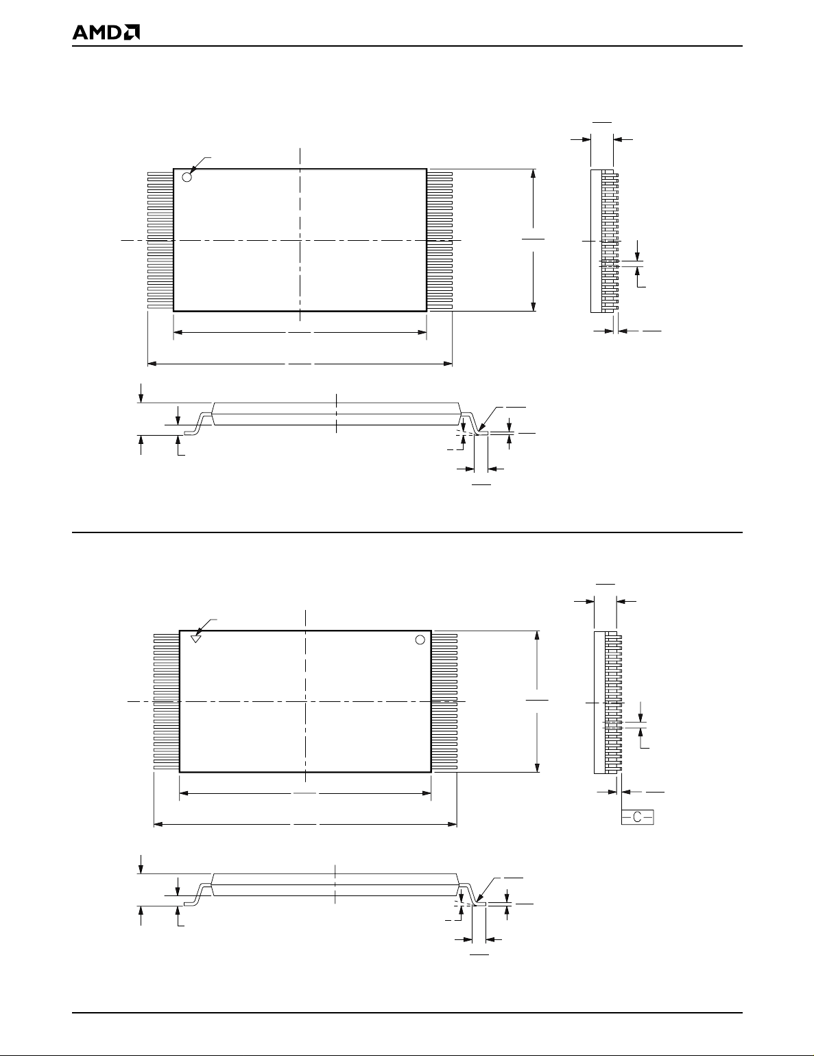
PRELIMINARY
PHYSICAL DIMENSIONS*
TS 048—48-Pin Standard TSOP (measured in millimeters)
Pin 1 I.D.
1
24
18.30
18.50
19.80
20.20
1.20
MAX
0.25MM (0.0098") BSC
* For reference only. BSC is an ANSI standard for Basic Space Centering
48
25
0°
5°
0.50
0.70
0.08
0.20
11.90
12.10
0.10
0.21
0.95
1.05
0.50 BSC
0.05
0.15
16-038-TS48-2
TS 048
DT95
8-8-96 lv
TSR048—48-Pin Reverse TSOP (measured in millimeters)
Pin 1 I.D.
1
24
18.30
18.50
19.80
20.20
1.20
MAX
0.25MM (0.0098") BSC
* For reference only. BSC is an ANSI standard for Basic Space Centering.
48
25
0°
5°
0.50
0.70
11.90
12.10
0.08
0.20
0.10
0.21
0.95
1.05
SEATING PLANE
0.50 BSC
0.05
0.15
16-038-TS48
TSR048
DT95
8-8-96 lv
40 Am29DL800B
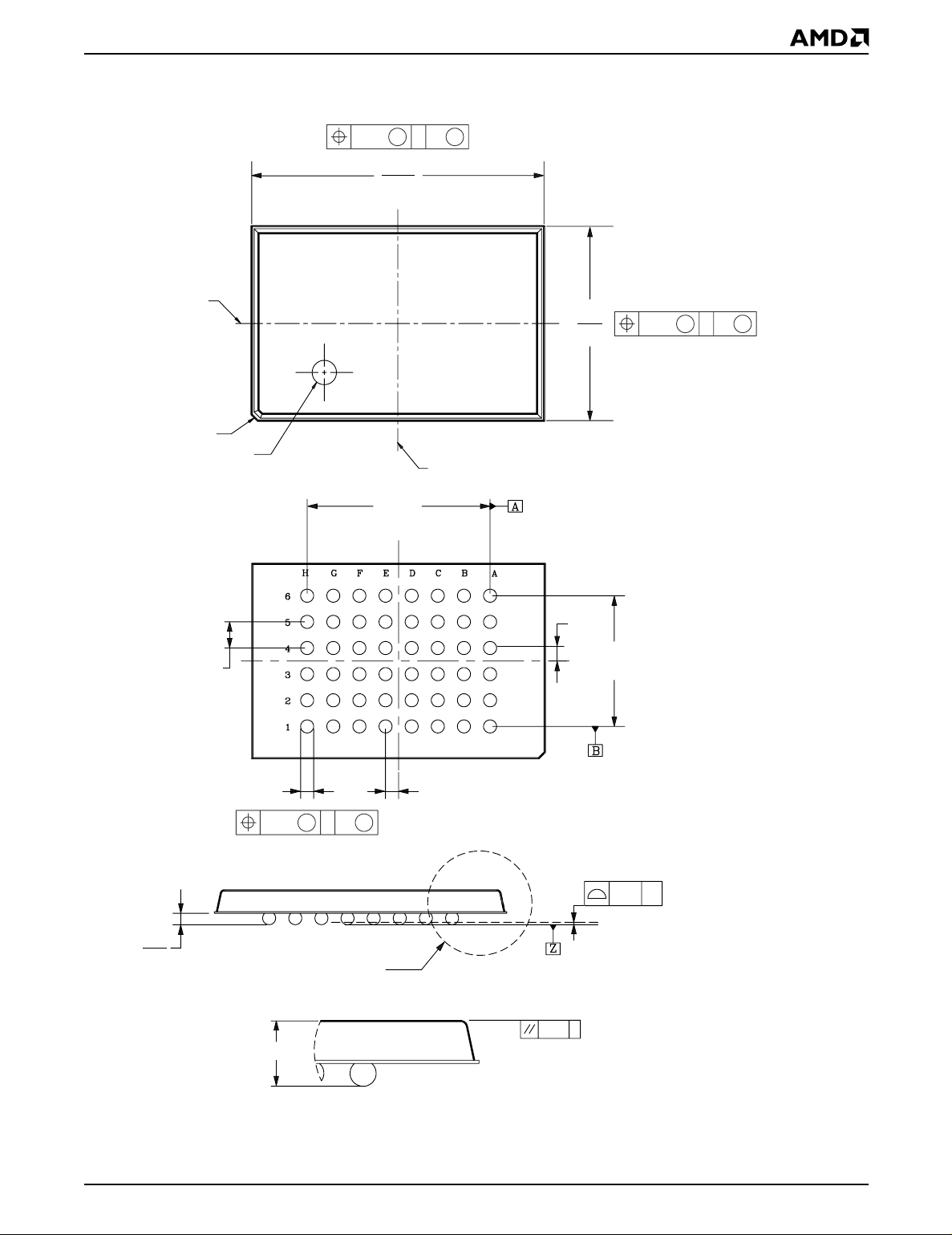
PRELIMINARY
PHYSICAL DIMENSIONS (continued)
FGB048 —48-ball Fine-Pitch Ball Grid Array (FBGA), 6 x 9 mm (measured in mm)
M
B
0.15
8.80
9.20
M
Z
DATUM B
0.025
CHAMFER
0.80
INDEX
5.60
BSC
DATUM A
5.80
6.20
0.40
4.00
BSC
0.15
M
B
M
Z
0.40 ± 0.08 (48x) 0.40
0.08MZA
0.25
0.45
1.20 MAX
B
DETAIL A
0.10 Z
0.20 Z
DETAIL A
16-038-FGB-2
EG137
12-2-97 lv
Am29DL800B 41

PRELIMINARY
PHYSICAL DIMENSIONS (continued)
SO 044—44-Pin Small Outline (measured in millimeters)
2.17
2.45
44
23
13.10
13.50
1
1.27 NOM.
TOP VIEW
28.00
28.40
0.35
0.50
SIDE VIEW
22
0.10
0.35
2.80
MAX.
15.70
16.30
SEATING
PLANE
0°
8°
0.10
0.21
0.60
1.00
END VIEW
16-038-SO44-2
SO 044
DF83
8-8-96 lv
42 Am29DL800B

PRELIMINARY
REVISION SUMMARY FOR AM29DL800B
Revision A+1
Reset Command
Deleted last paragraph in section, which applied to RESET#, not the reset command.
Revision A+2
Hardware Reset (RESET#)
Added note to table, fixed references to note.
Revision A+3
Global
Removed references to the 80 ns speed option.
Changed the 70R ns (V
70 ns (V
± 10%) speed option.
CC
Figure 2, In-System Sector Protect/Unprotect Algorithms
In the sector protect algorithm, added a “Reset
PLSCNT=1” box in the path from “Protect ano ther sector?” back to setting up the next sec tor address.
DQ6: Toggle Bit I
In the first and second paragraphs, clarified that the
toggle bit may be read “at any address within the pro-
± 5%) speed option to the
CC
gramming or erasing bank,” no t “at any add ress.” In the
fourth paragraph, clarified “device” to “bank.”
DC Characteristics
Added reference to Note 4 on I
CC6
and I
specifica-
CC7
tions.
AC Characteristics
Erase/Program Operations; Altern ate CE# Controlled
Erase/Program Operations:
ence for t
WHWH1
and t
100% tested. Corrected the note reference for t
Corrected the notes refer-
. These parameters are
WHWH2
VCS
This parameter is not 100% tested.
Temporary Sector Unprotect Table
Added note reference for t
. This parameter is not
VIDR
100% tested.
Figure 24, Sector Protect/Unprotect Timing Diagram
A valid address is not required for the first write cycle;
only the data 60h.
Erase and Programming Performance
In Note 2, the worst case endurance is now 1 million cycles.
.
Trademarks
Copyright © 1998 Advanced Micro Devices, Inc. All rights reserved.
AMD, the AMD logo, and combinations thereof are registered trademarks of Advanced Micro Devices, Inc.
ExpressFlash is a trademark of Advanced Micro Devices, Inc.
Product names used in this publication are for identification purposes only and may be trademarks of their respective companies.
Am29DL800B 43
 Loading...