

AMD Advanced Micro Devices AM28F512-90PIB, AM28F512-90PI, AM28F512-90PEB, AM28F512-90FI, AM28F512-90FE Datasheet
...
FINAL
Am28F512
512 Kilobi t ( 64 K x 8-Bit)
CMOS 12.0 Volt, Bulk Erase Flash Memory
DISTINCTIVE CHARACTERISTICS
■
High performance
— 70 ns maximum access time
■
CMOS Low power consumption
— 30 mA max imum act ive current
— 100 µA maximum standby current
— No data retention power consumption
■
Compatible with JEDEC-standard byte-wide
32-Pin EPROM pino uts
— 32-pin PDIP
— 32-pin PLCC
— 32-pin TSOP
■
10,000 write/erase cycles minimum
■
Write and erase voltage 12.0 V ±5%
■
■
■
■
■
■
■
Latch-up protected to 100 mA
from -1 V to V
Flasherase Electrical Bulk Chip-Erase
— One second typical chip-erase
Flashrite Programming
— 10 µs typical byte-program
— One second typical chip program
Command regist er architecture for
microprocessor/microcontroller compatible
write interface
On-chi p add r es s and dat a latches
Advanced CMOS flash memory technology
— Low cost single transistor memory cell
Aut o matic write/eras e pulse sto p timer
CC
+1 V
GENERAL DESCRIPTION
The Am2 8F512 is a 512 K bi t Flash me mory or ganized as 64 Kbytes of 8 bits each. AMD’s Flash memories offer the most cost-effective and reliable read/
write non-volatile random access memory. The
Am28F51 2 is packaged in 32-pin PDIP, P LCC, and
TSOP versio ns. It is designed to b e reprogrammed
and erased in-system or in standard EPROM programmers. The Am28F 512 is erased when sh ipped
from the factory.
The standard Am28F512 offers access times as fast as
70 ns, allowing operation of high-speed microprocessors without wait states. To eliminate bus contention,
the Am28F512 has separate chip enable (CE#) and
output enable (OE#) controls.
AMD’s Flash memories augment EPROM funct ionality
with i n-circuit elec trical e rasure and programming. The
Am28F512 uses a command register to manage this
functionality, while maintaining a standard JEDEC
Flash Standard 32-pin pinout. The command register
allows for 100% TTL level control inputs and fixed
power supply levels during erase and programming.
AMD’s Flash technology reliably stores memory contents even after 10,000 erase and program cycles. The
AMD cell is designed to optimize the erase and pro-
gra mmin g m ec han i sms . I n ad di t io n, th e c o mbin a tio n of
advanced t unnel oxide pr ocessi ng and low in ternal
electric fields for erase and programming operations
produces reliable cycling. The Am28F 512 uses a
12.0 V± 5% VPP high voltage input to per form the
Flashera se and Flashrit e algorithms.
The highest degree of latch-up protection is achieved
with AMD’s prop r ietary non -e pi pr oc e ss. Lat ch- up pro tection is provided for stresses up to 100 mA on address and data pins from -1 V to VCC +1 V.
The Am28F512 is byte programmable using 10 ms programmin g pul ses in acco rdance with A MD’s Flas hrit e
programming algorithm. The typical room temperature
programming time of the Am28F 512 is one s econd.
The en tire chip is b ul k er as ed u sing 10 m s era se puls es
according to AMD’s Flasherase algorithm. Typical erasure at room temperature is accomplished in less than
one second. The wi ndowed package and the 15-20
minutes required for EPROM erasure usi ng ultra-vio let
light are eliminated.
Commands are wr itten to the command register using
standard microprocessor write timings. Register contents serve as inputs to an internal state-machine which
controls the erase and programming circuitry. During
Publication#
Issu e Date:
Rev: GAmendment/
11561
January 1998
+2
write cycles, the command register internally latches
address and data needed for the pro gramming and
erase operations. For system design simplification, the
Am28F512 is designed to s uppor t either W E# or CE#
controlled writes. During a system write cycle, addresses are latched on the falling edge of WE# or CE#
whichever occurs last. Data is latched on the rising edge
of WE# or CE# whichever occurs first. To simplify the following discussion, the WE# pin is used as the write cycle
control pin throughout the rest of this text. All setup and
hold times are with respect to the WE# signal.
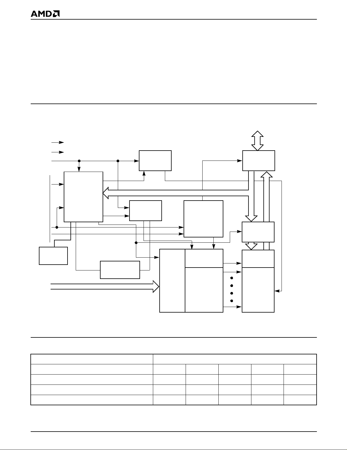
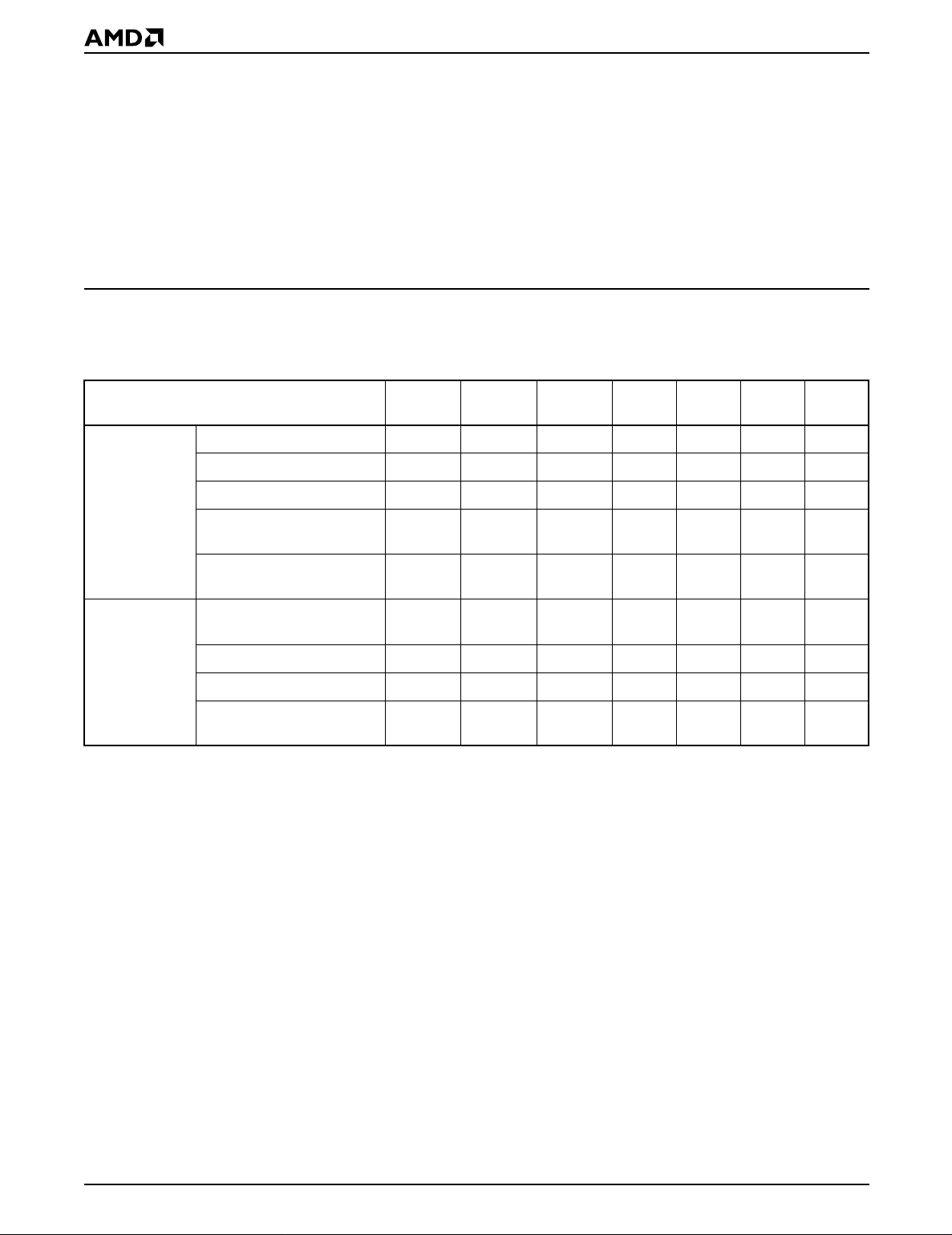
BLOCK DIAGRAM
V
CC
V
SS
V
PP
Erase
Voltage
Switch
AMD’s Flash technology combines years of EPROM
and EEPROM experience to produce the highest levels
of quality, reliability, and cost effectiveness. Th e
Am28F512 electrically erases all bits simultaneously
using Fowler-Nordheim tunneling. The bytes are programmed one byte at a time using the EPROM
programming mechanism of hot electron injection.
DQ0–DQ7
Input/Output
Buffers
WE#
CE#
OE#
Low V
Detector
A0–A15
CC
State
Control
Command
Register
Program/Erase
Pulse Timer
Program
Voltage
Switch
To Array
Address
Latch
Chip Enable
Output Enable
Logic
Y-Decoder
X-Decoder
Data
Latch
Y-Gating
524,288
Bit
Cell Matrix
11561G-1
PRODUCT SELECTOR GUIDE
Family Part Number
Speed Options (V
Max Access Time (ns) 70 90 120 150 200
CE# (E#) Access (ns) 70 90 120 150 200
OE# (G#) Access (ns) 35 35 50 55 55
= 5.0 V ± 10%)
CC
-70 -90 -120 -150 -200
2 Am28F512
Am28F512
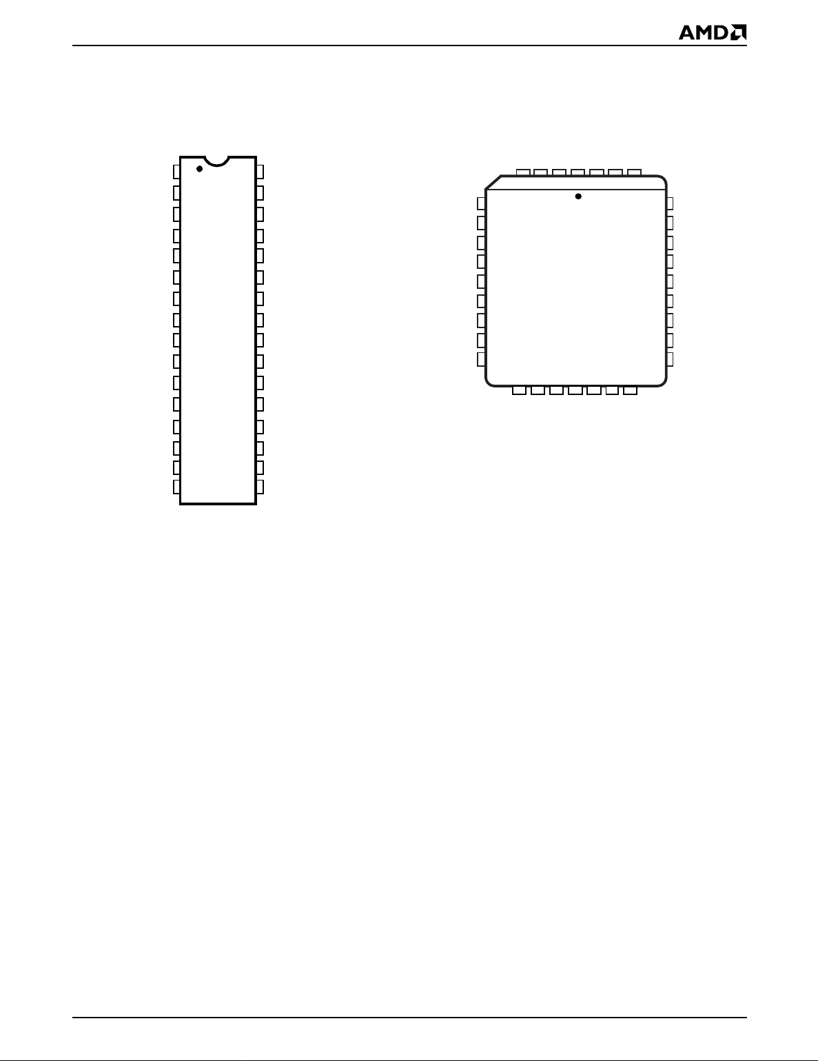
CONNECTION DIAGRAMS
V
PP
NC
A15
A12
A7
A6
A5
A4
A3
A2
A1
A0
DQ0
DQ1
DQ2
V
SS
1
2
3
4
5
6
7
8
9
10
11
12
13
14
15
16
PDIP
32
31
30
29
28
27
26
25
24
23
22
21
20
19
18
17
V
CC
WE# (W#)
NC
A14
A13
A8
A9
A11
OE# (G#)
A10
CE# (E#)
DQ7
DQ6
DQ5
DQ4
DQ3
11561G-2
A7
A6
A5
A4
A3
A2
A1
A0
DQ0
5
6
7
8
9
10
11
12
13
14
A12
4
DQ1
15
A15
3
DQ2
PLCC
NC
2
17
SS
V
PP
V
VCCWE# (W#)
31 30
1
32
19 2016
18
DQ4
DQ3
DQ5
NC
29
28
27
26
25
24
23
22
21
DQ6
A14
A13
A8
A9
A11
OE# (G#)
A10
CE# (E#)
DQ7
11561G-3
Note:
Pin 1 is marked for orientation.
Am28F512 3
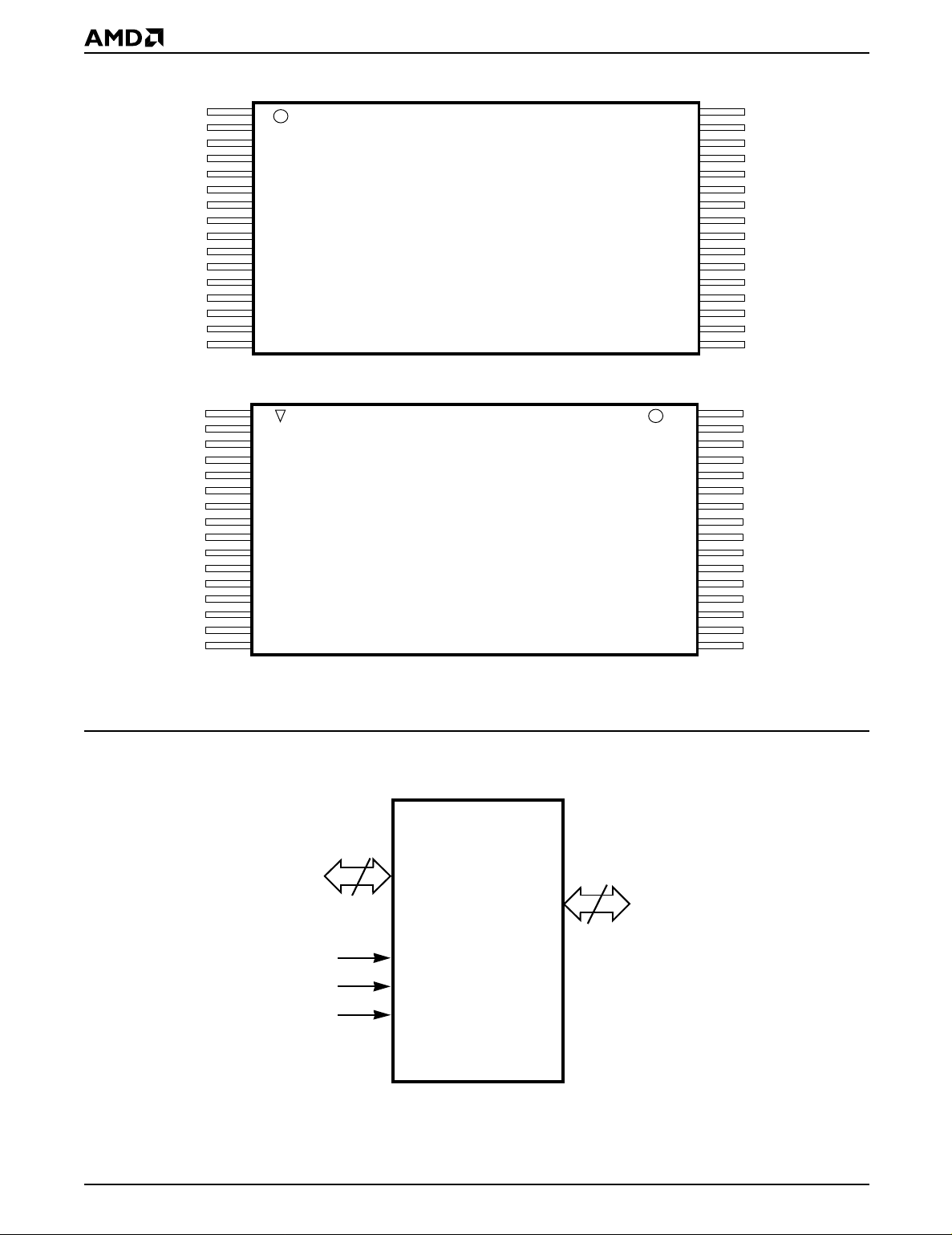
CONNECTION DIAGRAMS (contin ued)
A11
A13
A14
NC
WE#
V
V
NC
A15
A12
OE#
A10
CE#
D7
D6
D5
D4
D3
V
SS
D2
D1
D0
A0
A1
A2
A3
A9
A8
CC
PP
A7
A6
A5
A4
1
2
3
4
5
6
7
8
9
10
11
12
13
14
15
16
1
2
3
4
5
6
7
8
9
10
11
12
13
14
15
16
32-Pin — Standard Pinout
32
31
30
29
28
27
26
25
24
23
22
21
20
19
18
17
32
31
30
29
28
27
26
25
24
23
22
21
20
19
18
17
OE#
A10
CE#
D7
D6
D5
D4
D3
V
SS
D2
D1
D0
A0
A1
A2
A3
A11
A9
A8
A13
A14
NC
WE#
V
CC
V
PP
NC
A15
A12
A7
A6
A5
A4
LOGIC SYMBOL
32-Pin — Reverse Pinout
16
A0–A15
CE# (E#)
OE# (G#)
WE# (W#)
11561G-4
8
DQ0–DQ7
11561G-5
4 Am28F512
ORDERIN G IN FOR MATION
Standard Products
AMD standard products are available in several packages and operating ranges. The order number (V alid Combination) is formed
by a combination of:
AM28F512 -70 J C
DEVICE NUMBER/DESCRIPTION
Am28F512
512 Kilobit (64 K x 8-Bit) CMOS Flash Memory
B
OPTIONAL PROCESSING
Blank = Standard Processing
B = Burn-In
Contact an AMD representative for more information.
TEMPERATURE RANGE
C = Commercial (0°C to +70°C)
I = Industrial (–40°C to +85°C)
E = Extended (–55°C to +125°C)
PACKAGE TYPE
P = 32-Pin Plastic DIP (PD 032)
J = 32-Pin Rectangular Plastic Leaded Chip
Carrier (PL 032)
E = 32-Pin Thin Small Outline Package (TSOP)
Standard Pinout (TS 032)
F = 32-Pin Thin Small Outline Package (TSOP)
Reverse Pinout (TSR032)
SPEED OPTION
See Product Selector Guide and Valid Combinations
AM28F256-70
AM28F256-90
AM28F256-120
AM28F256-150
AM28F256-200
Valid Combinations
PC, PI, PE,
EC, EI, EE,
JC, JI, JE,
FC, FI, FE
Valid Combinations
Valid Combinations list configurations planned to be supported in volume for this device. Consult the local AMD sales
office to confirm availability of specific valid combinations and
to check on newly released combinations.
Am28F512 5

PIN DESCRIPTION
A0–A15
Address In puts for memor y lo cations. Inte rnal la tches
hold addresses during write cycles.
CE# (E#)
Chip Enable active low input activates the chip’s control
logic and input buffers. Chip Enable high will deselect
the device and operates the chip in stand-by mode.
DQ0–DQ7
Data Inputs during memory write cycles. Internal
latches hold data during write cycles. Data Outputs
during memory read cycles.
NC
No Conn ect- corre spond ing pin i s no t conn ec ted in ternally to the die.
OE# (G#)
Output Enable active low input gates the outputs of the
device through the data buffers during memory read
cycles. Output Enable is high during command sequencing and program/erase operations.
V
CC
Po w er supp ly for de vi ce oper at ion . (5.0 V ± 5% or 10%)
V
PP
Program voltage i nput. VPP must be at hi g h vol ta ge in
order to write to the command register. The command
register controls all functions required to alter the memory array contents. Memory contents cannot be altered
when VPP ≤ V
V
SS
Ground
CC
+2 V.
WE# (W#)
Write Enable active low input controls the write function
of the command register to the memory array. The target address is latched on the falling edge of the Write
Enable pulse and the appropriate data is latched on the
rising edge of the pulse. Write Enable high inhibits writing to the device.
6 Am28F512

BASIC PRINCIPLES
The device uses 100% TTL-level control inputs to
manage th e command register. Erase and rep rogramming opera tions use a fixed 12.0 V ± 5% high
voltage input.
Read Only Memory
Without high VPP voltage, the device functions as a
read only memory and operates like a standard
EPROM. Th e control inpu ts still ma nage traditi onal
read, standby, output disable, and Auto select modes.
Command Register
The command register is enabled only when high voltage is applied to the VPP pin. The erase and reprogramming operations are only accessed via the
register. In addition, two-cycle commands are required
for erase and reprogramming op erations. The traditional read, standby, output disable, and Auto select
modes are available via the register.
The device’s com mand regi ster is wr itt en us ing standard microprocessor write timings. The register controls an internal state machine that manages all device
operations. For system design simplification, the device is designed to suppor t either WE# or CE# controlled writes. Durin g a system write cy cle, addresses
are latched on the falling edge of WE# or CE# whichever occurs last. Data is latched on the rising edge of
WE# or CE# whichever occur first. To simplify the following discussion, the WE# pin is used as the write
cycle control pin throughout the rest of this text. All
setup and hold times are with respect to the WE# signal.
Overview of Erase/Program Operations
Flasherase™ Sequence
A multiple step command sequence is required to
erase the Flash device (a two-cycle Erase command
and repeated one cycle verify commands).
Note: The Flash memory array must be completely
programmed to 0’s prior to erasure. Refer to the
Flashrite™ Programming Algorithm.
1. Erase S etup: Write the Setup Erase command to
the command register.
2. Erase: Wr it e the Erase com mand (sam e as Setu p
Erase command) to the command register again.
The seco nd comm an d i n it iat es t he er a s e o per at i o n.
The system software routines must now time-out
the erase pulse width (10 ms) prior to issuing the
Erase-ver ify command. An integrate d stop time r
prevents any possibility of overerasure.
3. Erase-Verify: Write the Erase-verify command to
the command register. This command terminates
the erase operation. After the erase operation,
each byte of the array must be verified. Address in-
formation must be supplied with the Erase-verify
command. This command verifies the margin and
outputs t he add re ssed b y te in o rde r to co mpar e th e
array data with FFh data (Byte erased).
After successful data verification the Erase-verify
command is written again with new address information. Each byte of the array is sequentially verified in this manner.
If data of the addressed loca tion is not verified, the
Erase sequence is repe ated until the entire array is
successfully verified or the sequence is repea ted
1000 times.
Flashrite Programming Sequence
A three step command sequence (a two-cycle Program
command and one cycle Verify command ) is required
to pr og r am a byte of t h e Fla sh arr ay. Refe r to th e Fl as hrite Algorit h m.
1. Program Setup: Write the Setup Program com-
mand to the command regist er.
2. Pr ogram: Write the Program command to the com-
mand register with the appropriate Address and
Data. The system software routines must now timeout the program pulse width (10 µs) prior to issuing
the Program-verify command. An integrated stop
timer prevents any possibility of overprogramming.
3. Program-Verify: Write the Program-verify com-
mand t o th e com ma nd register. Thi s command ter minates the programming op eration. In additio n,
this command verifies the margin and outputs the
byte just programmed in order to compare the array
data with the original data programmed. After successful d ata ver ification, the programm ing sequence is initiated again for the next byte address to
be programmed.
If data is n ot verified succes sfully, the Pr ogram sequence is repeated until a successful comparison is
verified or the sequence is repeated 25 times.
Data Protection
The device is designed to offer protection aga inst acci dental erasure or programming ca used by spurious
system level signals that may exist during power transitions . The d evice po wers up in it s r ea d onl y st at e . A ls o,
with its control register architecture, alteration of the
memory contents only occurs after successful completion of specific command sequences.
The device al so i ncor pora tes s everal feat ures t o pre vent inadvertent write cycles resulting fromVCC powerup and power-down transitions or system noise.
Low VCC Write Inhibit
To avoid initiation of a write cycle during VCC power-up
and power-d own, the d evice locks out wr ite cycl es for
Am28F512 7
VCC < V
voltages) . Wh en VCC < V
(see DC Characteristics section for
LKO
, the comm an d r eg i ster i s
LKO
disabled, all internal program/erase circuits are
disabled , an d th e d evice resets to the r ea d m od e. Th e
device ignores all writes until VCC > V
. The user
LKO
must ensure that the control pins are in the correct logic
state wh en VCC > V
to prevent uninitentional writes.
LKO
Write Pulse “Glitch” Protection
Noise pul se s of less than 10 ns (typical) on OE#, CE#
or WE# will not initiate a write cycle.
FUNCTIONAL DESCRIPTION
Description of User Modes
Table 1. Am28F512 User Bus Operations (Notes 7 and 8)
Operation CE# (E#)OE# (G#)WE# (W#)
Read-Only
Read V
Standby V
Output Disable V
Auto-select Manufacturer
Code (Note 2)
IL
IH
IL
V
IL
Logical Inhibit
Writing is inhibited by holding an y one of OE# = VIL, CE#
= VIH or WE# = VIH. To initiate a write cycle CE# a nd
WE# must be a logical zero while OE# is a logical one.
Power- U p Wr ite Inhibi t
Power-up of the device with W E# = CE# = VIL and
OE# = VIH will not accept commands on the r ising
edge of WE#. The internal state machine is automatically reset to the read mode on power-up.
V
PP
(Note 1) A0 A9 I/O
V
IL
XXV
V
IH
V
IL
XV
V
IH
V
IH
PPL
PPL
V
PPL
V
PPL
A0 A9 D
OUT
X X HIGH Z
X X HIGH Z
V
IL
V
(Note 3)
ID
CODE
(01H)
V
ID
(Note 3)
Read/Write
Auto-select Device Code
(Note 2)
Read V
Standby (Note 5) V
Output Disable V
Write V
V
IL
IL
IH
IL
IL
V
IL
V
IL
XXV
V
IH
V
IH
V
IH
V
IH
V
IH
V
IL
V
V
V
V
PPL
PPH
PPH
PPH
PPH
V
IH
A0 A9
X X HIGH Z
X X HIGH Z
A0 A9
Legend:
X = Don’t care, where Don’t Care is either V
levels of V
. 0 V < An < V
PPH
+ 2 V, (normal TTL or CMOS input levels, where n = 0 or 9).
CC
IL
levels. V
IH
PPL
= V
PP
< V
+ 2 V. See DC Characteristics for voltage
CC
or V
Notes:
1. V
may be grounded, connected with a resistor to ground, or < VCC +2.0 V. V
PPL
for the device. Refer to the DC characteristics. When V
PP
= V
, memory contents can be read but not written or erased.
PPL
is the programming voltage specified
PPH
2. Manufacturer and device codes may also be accessed via a command register write sequence. Refer to Table 2.
3. 11.5 < V
4. Read operation with V
5. With V
6. Refer to Table 3 for valid D
7. All inputs are Don’t Care unless otherwise stated, where Don’t Care is either V
< 13.0 V. Minimum V
ID
= V
PP
at high voltage, the standby current is ICC + I
PP
rise time and fall time (between 0 and VID voltages) is 500 ns.
ID
may access array data or the Auto select codes.
PPH
during a write operation.
IN
(standby).
PP
IL
or V
levels. In the Auto select mode all
IH
addresses except A9 and A0 must be held at VIL.
8. If V
≤ 1.0 Volt, the voltage difference between VPP and VCC should not exceed 10.0 Volts. Also, the Am28F512 has a V
CC
rise time and fall time specification of 500 ns minimum.
CODE
(25H)
D
OUT
(Note 4)
D
IN
(Note 6)
PP
8 Am28F512
READ ONLY MODE
When VPP is less than V
is inactive. The device can either read array or autoselect data, or be standby mode.
+ 2 V, the comm and regis ter
CC
Read
The device f unc t ion s as a r ea d o nly m em ory wh en V
< V
+ 2 V . The de v ice ha s tw o con tro l fu ncti ons . Bo th
CC
must be satisfied in order to output data. CE# controls
power to the d evice. This pin sh ould be used for specific device sele ctio n. OE# c ontro ls the device ou tputs
and shou ld be used to gate data to the output pin s if a
device is selected.
Address access time t
is equal to the delay from
ACC
stable addresses to valid ou tput data. Th e ch i p en able
access time tCE is the delay from stable addresses and
stable CE# to valid data at the output pins. The output
enable access time is the delay from the falling edge of
OE# to valid data at the output pins (assuming the addresses have been stable at least t
ACC–tOE
).
PP
Standby Mode
The device has two standby modes. The CMOS
standby mode (CE# input held at V
sumes less t han 100 µA o f c urr ent . TTL s ta ndb y mode
(CE# is held at VIH) reduces the current requirements
to less than 1mA. When in the standby mode the outputs are in a h igh imp eda nce s ta te , i nde pend ent of th e
OE# input.
If the device is deselected during eras ure, programming, or p rogram/erase verificati on, the device will
draw active current until the operation is terminated.
CC
±
0.5 V), con-
Output Dis a ble
Output from the device is disabled when OE# is at a
logic high level. When disabled, output pins are in a
high impedance state.
Auto Select
Flash memories can be programmed in-system or in a
standard PROM programmer. The device may be soldered to the circuit board upon receipt of shipment and
programmed in-system. Alternatively, the device may
initially be programmed in a PROM programmer pr ior
to soldering the device to the board.
The Auto select mode allows the reading out of a binary
code from the device that will identify its manufacturer
and type. T his mode is i ntended for the pu rpose
of automatically matching the device to be programmed with its corresp onding programming algorithm. This mode is functional over the entire
temperature range of the device.
Programming In A PROM Programmer
To activate thi s mode, the programmin g equipm ent
must force VID (11.5 V to 13.0 V ) on addre ss A9 . Two
identi fie r b yte s ma y th en be seq uence d fr om th e de vi ce
outpu ts b y t oggli ng addr ess A0 from VIL to VIH. All other
address lines must be held at VIL, and VPP must be
less than or equal to VCC + 2.0 V while using this Auto
select mode. Byte 0 (A0 = VIL) repr esen ts th e man uf acturer code and byte 1 (A0 = VIH) the device identifier
code. For the device these two bytes are given in Table
2 below. All identifiers for manufacturer and device
codes will exhibit odd parity with the MSB (DQ7) defined as the parity bit.
Table 2. Am28F512 Auto Select Code
Type A0 Code (HEX)
Manufacturer Code V
Device Code V
IL
IH
01
25
Am28F512 9
ERASE, PROGRAM, AND READ MODE
When VPP is equal to 12.0 V ± 5%, the command register is active. All fu nctions ar e available. Tha t is, the
device can program, erase, read array or autoselect
data, or be standby mode.
Write Operations
High voltage must be applied to the VPP pin in order to
activate the command register. Data written to the register serves as input to the internal state machine. The
output of the state machine determines the operational
function of the device.
Refer to AC Writ e Chara cteris tics and th e Erase/ Programming Waveforms for specific timing parameters.
Command Definitions
The contents of the command register default to 00h
(Read Mode) in the absence of high voltage applied to
the VPP pin. The device opera tes as a rea d only mem ory. High voltage on the VPP pin enables the co mma nd
regist e r. Device op er a t ion s ar e s e lec t e d by writin g s p ecific data codes into the command register. Table 3 defines thes e re gist e r com m and s.
The command register does not occupy an addressable
memory location. The register is a latch that stores the
command, along with the address and data information
needed to execute the command. The register is written
by bringing WE# and CE# to VIL, while OE# is at VIH.
Addresses are latched on the falling edge of WE#, while
data is latched on the rising edge of the WE# pulse.
Standard microprocessor write timings are used.
The device requires the OE# pin to be VIH for write operations. This condition eliminates the possibility for
bus contention during programming operations. In
order to write, OE# must be VIH, and CE# and WE#
must be VIL. If any pin is not in the correct state a write
command will not be executed.
Read Command
Memor y conte nts can be acces sed via th e read com mand when VPP is high. To read from the device, write
00h into the command register. Standard microprocessor read cycles access data from the memory. The device will remain in the read mode until the command
register contents are altered.
The comma nd register defaults to 00h (r ead mode)
upon VPP power -up . The 00h (Re ad Mode ) regis ter default helps ensure that inadvertent alteration of the
memory contents does not occur during the VPP power
transition. Refer to the AC Read Characteristics and
Waveform s for the spec ifi c timi n g para m ete rs.
Table 3. Am28F512 Command Definitions
First Bus Cycle Second Bus Cycle
Operation
Command (Note 4)
Read Memory Write X 00H/FFh Read RA RD
Read Auto select Write X 80h or 90h Read 00h/01h 01h/25h
(Note 1)
Address
(Note 2)
Data
(Note 3)
Operation
(Note 1)
Address
(Note 2)
Data
(Note 3)
Erase Set-up/Erase Write Write X 20h Write X 20h
Erase-Verify Write EA A0h Read X EVD
Program Set-up/ Program Write X 40h Write PA PD
Program-Verify Write X C0h Read X PVD
Reset Write X FFh Write X FFh
Notes:
1. Bus operations are defined in Table 1.
2. RA = Address of the memory location to be read.
EA = Address of the memory location to be read during erase-verify.
PA = Address of the memory location to be programmed.
X = Don’t care. Addresses are latched on the falling edge of the WE
3. RD = Data read from location RA during read operation.
EVD = Data read from location EA during erase-verify.
PD = Data to be programmed at location PA. Data latched on the rising edge of WE
PVD = Data read from location PA during program-verify. PA is latched on the Program command.
4. Refer to the appropriate section for algorithms and timing diagrams.
pulse.
#
.
#
10 Am28F512

FLASHERASE ERASE SEQUENCE
Erase Setup
Erase Setup is the first of a two-cycle erase command.
It is a com mand -only ope ration th at stag es the device
for bulk chip erase. T he array cont ent s are no t altere d
with t his co mma nd . 20 h is wri tte n t o t h e com ma nd re gister in order to perform the Erase Setup operation.
Erase
The seco nd two-cycle e rase comman d initiates th e
bulk erase operation. You must write the Erase command (20h) again to the register. The erase operation
begins with the rising edge of the WE# pulse. The
erase operation mu st be ter minated by writin g a new
command (Erase-verify) to the register .
This two ste p seq uenc e o f the Set up an d E rase c ommands h elps to ensure th at memo ry c ontents are not
accidentally eras ed . Al so, chi p e rasu re ca n only occ u r
when hig h vo ltag e is appl ied to the VPP pin an d al l c o ntrol pins are in their proper state. In absence of this high
voltage, me mor y contents c annot be altere d. Refer to
AC Erase Characteristics and Waveforms for specific
timing parame ters.
Note: The Flash memory device must be fully
programmed to 00h data prior to erasure. This
equalizes the charge on all memory cells ensuring
reliable era sure.
Erase-V erify Command
The erase op eration erases all bytes of the array
in pa ral lel. After the e ras e op era ti on , all byte s mu s t b e
sequentially verified. The Erase-verify operation is initi-
ated b y w ri tin g A 0 h to t he reg i s ter. The byte ad dr es s to
be verified must be supplied with the command. Addresses are latc hed on the falling edge of the WE #
pulse or CE# pulse, whichever occurs later. The rising
edge of the WE# pulse terminates the erase operation.
Margin Verify
During the Erase-verify operation, the device applies
an internally generated margin voltage to the
addressed byte. Reading FFh from the addressed byte
indicates that all bits in the byte are properly erased.
Verify Next Address
You must write the Erase-verify command with the appropriate address to the register prior to verification of
each address. Each new address is latched on the falling edge of WE# or CE# pulse, whichever occurs later.
The process co ntinues for each byte in the memor y
array until a byte does not return FFh data or all the
bytes in the array are accessed and verified.
If an address is not verified to FFh data, the entire chip
is erased again (refer to Erase Setup/Erase). Erase
verifica tion then resumes at the ad dress tha t failed to
verify. Erase is complete when all bytes in the array
have been verified. The device is now ready to be programmed. At this point, the verification operation is terminated by writing a valid command (e.g. Program
Setup) to the command register. Figure 1 and Table 4,
the Flasherase electrical erase algorithm, illustrate how
commands and bus operations are combined to perform electrical erasure. Refer to AC Erase Characteristics and Waveforms for specific timing parameters.
Am28F512 11

Start
Yes
Data = 00h
No
Program All Bytes to 00h
Apply V
PPH
Address = 00h
PLSCNT = 0
Write Erase Setup Command
Write Erase Command
Time out 10 ms
Write Erase Verify
Time out 6 µs
Read Data from Device
No
PLSCNT =
Apply V
Erase Error
No
1000
Increment
PLSCNT
Yes
PPL
Data = FFh
Yes
Last Address
Yes
Write Reset Command
Apply V
PPL
Erasure Completed
Figure 1. Flashera se Electrical Erase Algorithm
No
Increment Address
11559G-6
12 Am28F512

Flasherase Electrical Erase Algorithm
This Flash memory device erases the entire array in
parallel . Th e era s e tim e de pe nd s on VPP, temperature,
and number o f erase /program cycle s on th e device. In
general, reprogramming time increases as the number
of erase/program cycles increases.
The Flasherase electrical erase algorithm employs an
interact ive clo sed lo op flow to simul ta ne ou s ly erase all
bits in the array . Erasure begins with a read of the memory conte nt s. The dev ice i s era sed wh en shipped from
the factory. Reading FFh data from the device would
immedi at el y be f o l lo w ed b y e xecutin g t he Fla s hrit e pr ogramming algorithm with the appropriate data pattern.
Should the device be currently programmed, data other
than FFh will be returned from address locations.
Follow the Fla sherase algor ithm. Uniform and reli able
erasure is en sured by fir st programm ing all bits i n the
device to their charged state (Data = 00h). This is
accomplished using the Flashr ite Programming
Table 4. Flasherase Electrical Erase Algorithm
Bus Operations Command Comments
algorithm. Erasure then continues with an initial erase
operation. Erase verification (Data = FFh) begins at
addres s 0 00 0h and co ntinues thro ugh t he array to the
last address, or until data other than FFh is
encountered. If a byte fails to verify, the device is
erased again. With each erase operation, an
increasing number of bytes verify to the erased state.
Typically, devices are erased in less than 100 pulses
(one second). Erase efficie ncy may be improved by
storing the address of the last byte that fails to verify in
a regist er. Following the next erase operation,
verification may start at the store d address location . A
total of 1000 erase pulses are allowed per reprogram
cycle, which corresponds to approximately 10 seconds
of cumul at iv e era se tim e. The ent ire se quen ce of era se
and byte verificat ion is performed with high voltage
applied to the VPP pin. Figure 1 illustrates the electrical
eras e algorithm.
Entire memory must = 00h before erasure (Note 3)
Note: Use Flashrite
programming.
Wait for V
Standby
Write
Standby Duration of Erase Operation (t
Write Erase-Verify (Note 2)
Standby Write Recovery Time before Read = 6 µs
Read Read byte to verify erasure
Standby
Write Reset Data = FFh, reset the register for read operations
Standby Wait for V
Notes:
1. See AC and DC Characteristics for values of V
switchable. When V
2. Erase Verify is performed only after chip erasure. A final read compare may be performed (optional) after the register is written
with the read command.
3. The erase algorithm Must Be Followed to ensure proper and reliable operation of the device.
Erase Setup Data = 20h
Erase Data = 20h
parameters. The V
is switched, V
PP
PPL
PP
may be ground, no connect with a resistor tied to ground, or less than VCC + 2.0 V.
Initialize:
Addresses
PLSCNT (Pulse count)
Address = Byte to Verify
Data = A0h
Stops Erase Operation
Compare output to FFh
Increment pulse count
Ramp to V
PP
Ramp to V
PP
power supply can be hard-wired to the device or
PP
programming algorithm (Figure 3) for
(Note 1)
PPH
)
WHWH2
(Note 1)
PPL
Am28F512 13

Section
Addresses
CE
OE
WE
AB DEFCG
#
#
#
Data
Out
Compare
Data
Erase
Verific ation
Proceed per
Erase-
Verify
A0h
Transition
(6 µs)
Data
V
CC
V
PP
AB DEFCG
Bus Cycle Write Write Time-out Write Time-out Read Standby
Command 20h 20h N/A A0h N/A
Function
Erase
Setup
20h
Erase
20h
Erase
(10 ms)
Figure 2. AC Waveforms For Erase Operations
ANALYSIS OF ERASE TIMING WAVEFORM
Note: This analysis d oes not in clud e the requi rem ent
to pr og r am th e en t ire ar r ay to 00 h da ta p ri or t o era s ur e .
Refer to the Flashrite Programming algorithm.
Erase Setup/Erase
This analysis illustr ates the use of two-cycle erase
comman ds (section A and B). T he first era se command (20h) is a Setup command and does not affect
the array da ta (section A). The s econd erase command (20h) initiates the erase operation (section B)
on the rising edge of this WE# pulse. All bytes of the
memory array are erased in parallel . No address inf ormation is required.
The erase pulse occurs in section C.
Time-Out
A software timing routine (10 ms duration) must be initiate d on t he ris ing edge of the WE# pul se of s ecti on B .
Note: An integrated stop timer prevents any possibility of overerasure by limiting each time-out period of
10 ms.
Erase-V er ify
Upon co mpl etion of the era se sof tware timi ng r outine,
the microprocessor must write the Erase-verify command (A0 h). This c ommand termi nates the era se ope ration on the rising edge of the WE# pulse (section D).
The Erase-verify comm and also stages th e device for
data verific ation (section F).
11559G-7
N/A
Erase
Algorithm
After each erase operation each byte must be verified.
The byte address to be verified must be supplied with
14 Am28F512

the Erase-ver ify co mma nd (sec tion D). Ad dresse s are
latched on the falling edge of the WE# pulse.
Anothe r sof tw are t imin g rout ine (6 µs du rat ion) must be
executed to allow for generation of internal v oltages for
margin checking and read oper ation (section E) .
During Erase-verification (section F) each address that
returns FFh data is successfully erased. Each address
of the array is sequentially verified in this manner by repeating sections D thru F un til the entir e array is verified or an address fails to verify. Sho uld an address
FLASHRITE PROGRAMMING SEQUENCE
Program Setup
The device is programmed byte by byte. Bytes may be
programmed sequentially or at random. Program Setup
is the first of a two-cycle program command. It stages
the device for byte program ming. Th e Progra m Setu p
operation is performed by writing 40h to the command
register.
Program
Only after the program Setup operation is completed
will the next WE# pulse initiate the active programming
operation. The appropriate address and data for programming must be available on the second WE# pulse.
Addresses and data are internally latched on the falling
and rising edge of the WE# pulse respectively. The rising edg e o f WE# also begin s the pro gram min g op era tion. You must write the Program-verify command to
terminate the programming operation. This two step
sequen ce o f the Setu p and Program co mmands help s
to ensure that memory contents are not accidentally
written. Also, programming can only occur when high
vol tage is ap plie d to th e VPP pin an d al l c on tr ol pins are
in their proper state. In absence of this high voltage,
memory contents cannot be pr ogrammed.
Refer to AC Characteristics and W av ef orms for specific
timing parame ters.
Program Verify Command
Following each programming operation, the byte just
programm e d must be ver if ie d.
Write C0h into the command register in order to initiate
the Program-verify operation. The rising edge of this
WE pulse te rm ina tes the p rogram min g opera tion. The
location fail to verify to FFh data, erase the device
again. Repeat sections A thru F. Resume verification
(secti on D) wi th the failed add re ss.
Each da ta change se quence al lows the devic e to use
up to 1,000 erase pulses to completely erase. Typically
100 eras e pulses are required.
Note: All address locations must be programmed to
00h prior to erase. This equa lizes the charge on all
memory cells and ens u re s reli able era s ur e.
Program-verify operation stages the device for verification of the last byte programmed. Addresses were previously latched. No new information is required.
Margin Verify
During the P rog ra m-v erif y ope rat ion, th e de vi ce ap pli es
an internally gen erated margin voltage to the addressed byte. A normal microprocessor read cycle outputs the data. A successful comparison between the
programme d byte and the tr ue data indicate s that the
byte was successfully programmed. The original programmed data should be stored for comparison. Programming then proceeds to the next desired byte
location. S h ou l d th e byte fail to ver ify, reprogram (refer
to Program Setup/Program). Figure 3 and Table 5 indicate how ins tr u ctions are com bin ed w it h th e bus op er ations to perform byte programm ing. Refer to AC
Programming Characteristics and Waveforms for specific timing parameters.
Flashrite Programming Algorithm
The device Flashrit e Programm ing a lgorith m empl oys
an interactive closed loop flow to program data byte by
byte. Bytes may be programmed sequentially or at random. The Flashrite Programming algorithm uses 10 µs
programming pulses. Each operation is followed by a
byte verification to determine when the addressed byte
has been successfully programmed. The program algorithm allows for up to 25 programming operations per
byte per repro gramming cycle. Most byte s verify after
the first or second pul se. The entir e sequen ce of programming and byte verific ation is per formed wit h high
voltage appl ie d to th e VPP pin. Figure 3 and Table 5 i llustrate the programming algorithm.
Am28F512 15

Increment Address
Start
Apply V
PPH
PLSCNT = 0
Write Program Setup Command
Write Program Command (A/D)
Time out 10 µs
Write Program Verify Command
Time out 6 µs
Read Data from Device
Verify Byte
No
Yes
No
Last Address
Yes
Write Reset Command
Increment PLSCNT
No
PLSCNT =
25?
Yes
Apply V
PPL
Programming Completed
Figure 3. Flashrite Programming Algorithm
Apply V
PPL
Device Failed
11559G-8
16 Am28F512

Table 5. Flashrite Programming Algorithm
Bus Operations Command Comments
Standby
Wait for V
Ramp to V
PP
Initialize Pulse counter
PPH
(Note 1)
Program Setup Data = 40h
Write
Program Valid Address/Data
Standby Duration of Programming Operation (t
WHWH1
)
Write Program-Verify (Note 2) Data = C0h Stops Program Operation
Standby Write Recovery Time before Read = 6 µs
Read Read Byte to Verify Programming
Standby Compare Data Output to Data Expected
Write Reset Data = FFh, resets the register for read operations.
Standby Wait for V
Ramp to V
PP
PPL
(Note 1)
Notes:
1. See AC and DC Characteristics for values of V
switchable. When V
is switched, V
PP
may be ground, no connect with a resistor tied to ground, or less than VCC + 2.0 V.
PPL
parameters. The V
PP
power supply can be hard-wired to the device or
PP
2. Program V erify is performed only after byte programming. A final read/compare may be performed (optional) after the register
is written with the read command.
Am28F512 17

Section
Addresses
CE
OE
WE
A
B
DE FCG
#
#
#
Data
V
CC
V
PP
AB DEFCG
Bus Cycle Write Write Time-out Write Time-out Read Standby
Command 40h
Function
Program
Setup
20h
Program
Address,
Program Data
Program
Command
Latch
Address and
Data
Data
In
N/A
Program
(10 µs)
A0h
C0h
(Stops
Program)
Program
Verify
N/A
Transi tion
(6 µs)
Data
Out
Compare
Data
Program
Verific ation
11559G-9
N/A
Proceed per
Programming
Algorithm
Figure 4. AC Waveforms for Programmin g Operations
ANALYSIS OF PROGRAM TIMING WAVEFORMS
Program Setup/Program
Two-cycle write commands are required for program
operations (section A and B). The first program command (40h) is a Setu p comm and an d do es not a ffect
the array data (section A).The second program command latch es addr ess and data req uired for programming on the falling and rising edge of WE# respectively
(section B). The rising edge of this WE# pulse (section
B) also initiates the programming pulse. The device is
programmed on a byte by byte basis either sequentially
or randomly.
The program pulse occurs in section C.
Time-Out
A software timing routine (10 µs duration) must be initiated on the rising edge of the WE# pulse of section B.
Note: An integ rated stop timer pre v ents an y possibility
of overprogramming by limiting each time-out period of
10 µs .
Program-Verify
Upon completion of the program timing routine, the microprocessor must write the program- verify command
(C0h). This command terminates the programming operation on the rising edge of the WE# pulse (section D).
The program-verify command also stages the device
fo r data v eri fica tion (s ecti on F ). An oth er s oft war e ti ming
routine (6 µs duration) must be executed to allow for
18 Am28F512

gener a ti on o f int e rnal v o l tag es for mar gin c h ecking a nd
read operations (section E).
During program-verification (section F) each byte just
programmed is read to compare array data with original
program data. When successfully verified, the next desired address is programmed. Should a byte fail to verify, repro gram th e byte (r epeat section A thr u F ) . E ac h
data ch ange sequ enc e a llows th e devic e to use up t o
25 progr am puls es p er b yte . Typicall y, byt es ar e v eri fied
within one or two pulses.
Parallel Device Erasure
Many applica tions will us e more than one Flash
memory device. Total erase t ime may be minimized by
implementing a parallel erase algorithm. Flash
memories may erase at different rates. Theref ore each
device must be verified separately. When a device is
completely erased and verified use a masking code to
prevent further erasure. The other devices will continue
to er ase until verified. Th e masking code applied could
be the read command (00h).
Algorithm Timing Delays
There are four different timing delays associated with
the Flasherase and Flashrite algorithms:
1. The first delay is associated with the VPP rise-time
when VPP first tur ns on. Th e ca pa ci to rs o n th e V
bus cause an RC ram p. Afte r switc hin g on the VPP,
the de lay requir ed i s pro por tio nal to the numbe r o f
device s being eras ed and the 0. 1 mF/d evice. V
must reach it s fin al valu e 10 0 ns be fore c om m and s
are executed.
2. The second delay time is the erase time pulse width
(10 ms). A software timing routine should be run by
the local m icropr ocessor to ti me out th e delay. The
erase op eration mus t be te rmina ted at the conclu sion of the ti ming ro utine or prior to executing any
system interrupts that may occur during the erase
operation. To ensure proper device operation, write
the Erase-verify operation after each pulse.
3. A third delay t ime is required for each programming
pulse w idth (10 ms) . The programming algorithm is
interactive and verifies each byte after a program
pulse. The program operation must be terminated at
the conclusion of the timing routine or prior to executing any system interrupts that may occur during
the programming operation.
4. A fourth timing delay associated with both the
Flasherase and Flashrite algorithms is the write recovery time (6 ms). During this time internal circuitry
is chan ging volt age levels fro m the e rase/ program
level to those used for margin verify and read operations. An at t emp t t o re ad t he device du ring t hi s p eriod will result in possible false data (it may appear
the device is not properly erased or programmed).
PP
PP
Po wer-Up/Power-Do wn Sequence
The device powers -up in th e Rea d only mode. Power
supply sequencing is not required. Note that if VCC ≤
1.0 Volt, the voltage difference between V
should not exceed 10.0 Volts. Also, the device has V
rise time and fall t i me sp ec ifi cat i on of 500 n s mi nim um.
PP
and V
CC
PP
Reset Command
The Reset comm and initializes the Flash m emor y device to the Read mode. In addition, it also provides the
user with a safe method to abort any device operation
(including program or erase).
The Rese t comm an d must b e wri tten two co nsecut ive
times after the setup Program command (40h). This will
reset the device to the Read mode.
Following any other Flash command write the Reset
command once to the de vice . Thi s will s afel y abort any
previous operation and initialize the device to the
Read mode.
The Setup Program command (40h) is the only command that requires a two sequence reset cycle. The
first Reset command is interpreted as program data.
However, FF h data is c o nsidered nu ll data du r ing programming operations (memory cells are only programmed from a logical “1” to “0”). T he second Reset
command safely abor ts the programmin g operation
and resets the device to the Read mode.
Memory contents are not altered in any case.
This deta iled inform ation is for your reference. It may
prove easier to alw ays issue the Rese t comman d two
consecutive times. This eliminates the need to determine if you are in the setup Program state or not.
Note: Software timing routines should be written in
machine language for each of the delays. Code written
in machine l anguage requires knowledge of the appropriate microprocessor c lock speed in order to accurately time each delay.
Am28F512 19
Programming In-System
Flash memories can be programmed in-system or in a
standard PROM programmer. The device may be soldered to the circuit board upon receipt of shipment and
programmed in-system. Alternatively, the device may
initially be programmed in a PROM programmer pr ior
to soldering the device to the board.

Auto Select Command
AMD’s Flash memories are designed for use in applications where the local CPU alters memory contents. Accordingly, manufacturer and device codes must be
accessible while the device resides in the target system. PROM programmers typically access the signature codes by raising A9 to a high voltage. However,
multiplexing high voltage onto address lines is not a
generally de si re d syst e m des ign practice.
The device contains an Auto Select operation to supplement traditional PROM programming methodology.
The operation is initiated by writing 80h or 90h into the
command r egister. Following this command, a read
cycle address 0000h retrieves the manufacturer code
of 01h. A read cycle from address 0001h returns the
device code. To terminate the operation, it is necessary
to write anothe r valid command, suc h a s R eset (FFh),
into the register.
20 Am28F512

ABSOLUTE MAXIMUM RATINGS
Storage T emperature . . . . . . . . . . . . –65°C to +150°C
Plastic Packages . . . . . . . . . . . . . . . –65°C to +125°C
Ambient Temperature
with Power Applied. . . . . . . . . . . . . .–55°C to + 125°C
Voltage with Respect To Ground
All pins except A9 and VPP (Note 1) .–2.0 V to +7.0 V
VCC (Note 1). . . . . . . . . . . . . . . . . . . .–2.0 V to +7.0 V
A9 (Note 2). . . . . . . . . . . . . . . . . . . .–2.0 V to +14.0 V
VPP (Note 2). . . . . . . . . . . . . . . . . . .–2.0 V to +14.0 V
Output Short Circuit Current (Note 3) . . . . . . 200 mA
Notes:
1. Minimum DC voltage on input or I/O pins is –0.5 V. During
voltage tr ansitions , inputs ma y ove rshoot V
periods of up to 20 ns. Maximum DC voltage on input and
I/O pins is V
I/O pins may overshoot to V
20ns.
2. Minimum DC input voltage on A9 and V
During voltage transitions, A9 and VPP may overshoot
V
to -2.0 V for periods of up to 20 ns. Maximum DC
SS
input voltage on A9 and VPP is +13.0 V which may
overshoot to 14.0 V for periods up to 20 ns.
3. No more than one output shorted to ground at a time.
Duration of the short circuit should not be greater than
one second.
Stresses above those listed under “Absolute Maximum
Ratings” may cause permanent damage to the device. This is
a stress rating only; functional operation of the device at
these or any other conditions above those indicated in the operational sections of this specification is not implied. Exposure of the device to absolute maximum rating conditions for
extended periods may affect device reliability.
+ 0.5 V. During voltage tra nsitions, i nput and
CC
+ 2.0V for periods up to
CC
to –2.0 V for
SS
pins is -0.5 V.
PP
OPERATING RANGES
Commercial (C) Devices
Ambient Temperature (TA). . . . . . . . . . . .0°C to +70°C
Industrial (I) Devices
Ambient Temperature (TA). . . . . . . . . .–40°C to +85°C
Extended (E) Devices
Ambient Temperature (TA). . . . . . . . .–55°C to +125°C
V
Supply Voltages
CC
VCC. . . . . . . . . . . . . . . . . . . . . . . . +4.50 V to +5.50 V
VPP Voltages
Read . . . . . . . . . . . . . . . . . . . . . . . . –0.5 V to +12.6 V
Program, Erase, and Verify. . . . . . +11.4 V to +12.6 V
Operating ranges define those limits between which the functionality of the device is guaranteed.
Am28F512 21

MAXI MUM OVERSHOOT
V
CC
+0.8 V
–0.5 V
+ 0.5 V
2.0 V
V
CC
20 ns
–2.0 V
20 ns
Maximum Negative Input Overshoot
20 ns
+ 2.0 V
20 ns 20 ns
20 ns
11561G-10
V
CC
11561G-11
Maximum Positive Input Overshoot
20 ns
14.0 V
13.5 V
+ 0.5 V
20 ns 20 ns
11561G-12
Maximum VPP Overshoot
22 Am28F512

DC CHARACTERISTICS over operating range unless otherwise specified
TTL/NMOS Compatible
Parameter
Symbol Parameter Description Test Conditions Min Typ Max Unit
I
I
I
I
I
V
V
V
I
I
LO
CCS
CC1
CC2
CC3
PPS
I
PP1
I
PP2
I
PP3
V
V
V
OH1
V
I
PPL
PPH
LI
OL
ID
Input Leakage Current V
Output Leakage Current VCC = VCC Max, V
VCC Standby Current VCC = VCC Max, CE# = V
VCC Active Read Current
VCC Programming Current
VCC Erase Current
V
Standby Current V
PP
V
Read Current
PP
V
Programming Current
PP
V
Erase Current
PP
Input Low Voltage –0.5 0.8 V
IL
Input High Voltage 2.0 VCC + 0.5 V
IH
= V
CC
V
CC = VCC
I
OUT
CE
#
Max, VIN = V
CC
Max, CE# = V
= 0 mA, at 6 MHz
= VIL
OUT
or V
CC
SS
= VCC or V
IH
OE# = V
IL,
Programming in Progress (Note 4)
CE
#
= VIL
Erasure in Progress (Note 4)
= V
PP
PPL
V
= V
PP
PPH
= V
V
PP
PPL
= V
V
PP
PPH
Programming in Progress (Note 4)
= V
V
PP
PPH
Erasure in Progress (Note 4)
SS
0.2 1.0 mA
IH
20 30 mA
20 30 mA
20 30 mA
70 200
10 30 mA
10 30 mA
Output Low Voltage IOL = 5.8 mA, VCC = VCC Min 0.45 V
Output High Voltage IOH = –2.5 mA, VCC = VCC Min 2.4 V
A9 Auto Select Voltage A9 = V
ID
ID
11.5 13.0 V
A9 Auto Select Current A9 = VID Max, VCC = VCC Max 5 50 µA
V
during Read-Only
PP
Operations
V
during Read/Write
PP
Operations
Note: Erase/Program are inhibited
PP
= V
PPL
when V
0.0 VCC +2.0 V
11.4 12.6 V
±1.0 µA
±1.0 µA
±1.0 µA
µA
±1.0
V
LKO
Low VCC Lock-out Voltage 3.2 3.7 V
Notes:
1. Caution: The Am28F512 must not be removed from (or inserted into) a socket when V
the voltage difference between V
and VCC should not exceed 10.0 Volts. Also, the Am28F512 has a VPP rise time and fall
PP
time specification of 500 ns minimum.
2. I
3. Maximum active power usage is the sum of I
is tested with OE# = VIH to simulate open outputs.
CC1
CC
and IPP.
4. Not 100% tested.
Am28F512 23
or VPP is applied. If VCC ð 1.0 V olt,
CC

DC CHARACTERISTICS
CMOS Compatible
Parameter
Symbol Parameter Description Test Conditions Min Typ Max Unit
I
I
I
I
I
V
V
V
V
I
I
LO
CCS
CC1
CC2
CC3
PPS
I
PP1
I
PP2
I
PP3
V
V
V
OH1
OH2
V
I
PPL
PPH
LI
OL
ID
Input Leakage Current V
Output Leakage Current VCC = VCC Max, V
VCC Standby Current VCC = VCC Max, CE
V
Active Read Current
CC
VCC Programming Current
VCC Erase Current
V
Standby Current V
PP
V
Read Current V
PP
V
Programming Current
PP
V
Erase Current
PP
Input Low Voltage –0.5 0.8 V
IL
Input High Voltage 0.7 V
IH
= V
Max, VIN = V
CC
= V
Max, CE# = V
CC
= 0 mA, at 6 MHz
= V
IL
V
I
OUT
CE
CC
CC
#
OUT
or V
CC
SS
= VCC or V
= VCC + 0.5 V 15 100 µA
#
OE# = V
IL,
Programming in Progress (Note 4)
CE
= V
#
IL
Erasure in Progress (Note 4)
= V
PP
PPL
= V
PP
PPH
= V
V
PP
PPH
Programming in Progress (Note 4)
V
= V
PPH
PP
Erasure in Progress (Note 4)
SS
IH
20 30 mA
20 30 mA
20 30 mA
70 200 µA
10 30 mA
10 30 mA
CC
Output Low Voltage IOL = 5.8 mA, VCC = VCC Min 0.45 V
Output High Voltage
A9 Auto Select Voltage A9 = V
ID
IOH = –2.5 mA, VCC = VCC Min 0.85 V
IOH = –100 µA, V
ID
= VCC Min VCC –0.4
CC
CC
11.5 13.0 V
A9 Auto Select Current A9 = VID Max, VCC = VCC Max 5 50 µA
V
during Read-Only
PP
Operations
V
during Read/Write
PP
Operations
Note: Erase/Program are inhibited
PP
= V
PPL
when V
0.0 VCC + 2.0 V
11.4 12.6 V
±1.0 µA
±1.0 µA
±1.0 µA
V
+ 0.5 V
CC
V
V
LKO
Low VCC Lock-out Voltage 3.2 3.7 V
Notes:
1. Caution: The Am28F512 must not be removed from (or inserted into) a socket when V
the voltage difference between V
and VCC should not exceed 10.0 volts. Also, the Am28F512 has a VPP rise time and fall
PP
time specification of 500 ns minimum.
2. I
3. Maximum active power usage is the sum of I
is tested with OE# = VIH to simulate open outputs.
CC1
CC
and IPP.
4. Not 100% tested.
24 Am28F512
or VPP is applied. If VCC ð 1.0 volt,
CC

25
20
15
Active in mA
10
CC
I
5
0
0123456789101112
Frequency in MHz
55°C
0°C
25°C
70°C
125°C
11561G-13
Figure 5 . Am28F5 12—Average ICC Active vs. Frequency
TEST CONDITIONS
Device
Under
Test
C
L
Note: Diodes are IN3064 or equivalent
Figure 6. Test Setup
6.2 k
VCC = 5.5 V, Addr essing Pattern = Minmax
Data Pattern = Checkerboard
Table 6. Test Specificat ions
5.0 V
2.7 k
Ω
Ω
11561G-14
Test Condition -70 All others Un it
Output Load 1 TTL gate
Output Load Capacitance, C
(including jig capacitance)
Input Rise and Fall Times
Input Pulse Levels 0.0–3.0 0.45–2.4 V
Input timing measurement
reference levels
Output timing measurement
reference levels
L
30 100 pF
10 ns
≤
1.5 0.8, 2.0 V
1.5 0.8, 2.0 V
Am28F512 25

SWITCHING TEST WAVEFORMS
s
2.4 V
0.45 V
2.0 V
Test Points
Input Output
2.0 V
0.8 V0.8 V
AC Testing (all speed options except -70): Inputs are driven at
2.4 V for a logic “1” and 0.45 V for a logic “0”. Input pulse rise
and fall times are
10 ns.
≤
3 V
1.5 V
0 V
Input Output
Test Points
AC Testing for -70 devices: Inputs are driven at 3.0 V for a
logic “1” and 0 V for a logic “0”. Input pulse rise and fall time
are ≤10 ns.
SWITCHING CHARACTERISTICS over operating range unless otherwise specified
AC Character istics—Read Only Operation
Parameter Symbols
t
AVAV
t
ELQV
t
AVQV
t
GLQV
t
ELQX
t
t
t
ACC
t
t
RC
CE
OE
LZ
Parameter Description
Read Cycle Time (Note 2) Min 70 90 120 150 200 ns
Chip Enable Access Time Max 70 90 120 150 200 ns
Address Access Time Max 70 90 120 150 200 ns
Output Enable Access Time Max 35 35 50 55 55 ns
Chip Enable to Output in Low Z
(Note 2)
Min00000ns
Am28F512
1.5 V
11561G-15
UnitJEDEC Standard -70 -90 -120 -150 -200
t
EHQZ
t
GLQX
t
GHQZ
t
AXQX
t
WHGL
t
VCS
t
t
DF
OLZ
t
DF
t
OH
Chip Disable to Output in High Z
(Note 1)
Output Enable to Output in Low Z
(Note 2)
Output Disable to Output in High Z
(Note 2)
Output Hold from first of Address,
CE#, or OE# Change (Note 2)
Write Recovery Time before Read Min 6 6 6 6 6 µs
VCC Setup Time to Valid Read
(Note 2)
Notes:
1. Guaranteed by design not tested.
2. Not 100% tested.
Max2020303535ns
Min00000ns
Max2020303535ns
Min00000ns
Min5050505050µs
26 Am28F512

AC Character istics—Write/Erase/Program Operations
Parameter Symbols
t
AVAV
t
AVWL
t
WLAX
t
DVWH
t
WHDX
t
WHGL
t
GHWL
t
ELWL
t
WHEH
t
WLWH
t
WHWL
t
WHWH1
t
WHWH2
t
VPEL
t
WC
t
AS
t
AH
t
DS
t
DH
t
WR
t
CS
t
CH
t
WP
t
WPH
Am28F512 Speed Options
Parameter Description
UnitJEDEC Standard -70 -90 -120 -150 -200
Write Cycle Time (Note 4) Min 70 90 120 150 200 ns
Address Setup Time Min 0 0 0 0 0 ns
Address Hold Time Min 45 45 50 60 75 ns
Data Setup Time Min 45 45 50 50 50 ns
Data Hold Time Min 10 10 10 10 10 ns
Write Recovery Time before Read Min 6 6 6 6 6 µs
Read Recovery Time before Write Min 0 0 0 0 0 µs
Chip Enable Setup Time Min 0 0 0 0 0 ns
Chip Enable Hold Time Min 0 0 0 0 0 ns
Write Pulse Width Min 45 45 50 60 60 ns
Write Pulse Width HIGH Min 20 20 20 20 20 ns
Duration of Programming Operation
(Note 2)
Min1010101010µs
Duration of Erase Operation (Note 2) Min 9.5 9.5 9.5 9.5 9.5 ms
VPP Setup Time to Chip Enable LOW
(Note 4)
Min 100 100 100 100 100 ns
t
VCS
t
VPPR
t
VPPF
t
LKO
VCC Setup Time to Chip Enable LOW
(Note 4)
VPP Rise Time 90% V
VPP Fall Time 10% V
VCC < V
to Reset (Note 4) Min 100 100 100 100 100 ns
LKO
(Note 4) Min 500 500 500 500 500 ns
PPH
(Note 4) Min 500 500 500 500 500 ns
PPL
Min5050505050µs
Notes:
1. Read timing characteristics during read/write operations are the same as during read-only operations. Refer to AC
Characteristics for Read Only operations.
2. Maximum pulse widths not required because the on-chip program/erase stop timer will terminate the pulse widths internally
on the device.
3. Chip-Enable Controlled Writes: Write operations are driven by the valid combination of Chip-Enable and Write-Enable. In
systems where Chip-Enable defines the Write Pulse Width (within a longer Write-Enable timing waveform) all setup, hold and
inactive Write-Enable times should be measured relative to the Chip-Enable waveform.
4. Not 100% tested.
Am28F512 27

KEY TO SWITCHING WAVEFORMS
WAVEFORM INPUTS OUTPUTS
Don’t Care, Any Change Permitted Changing, State Unknown
Does Not Apply Center Line is High Impedance State (High Z)
SWITCHING WAVEFORMS
Steady
Changing from H to L
Changing from L to H
Addresses
CE# (E#)
OE# (G#)
WE# (W#)
Data (DQ)
5.0 V
V
CC
0 V
Power-up, Standby
t
VCS
High Z High Z
Device and
Address Selection
Addresses Stable
t
WHGL
t
GLQV
t
(tCE)
ELQV
t
(tLZ)
ELQX
t
(t
AVQV
ACC
)
Outputs
Enabled
t
AVAV
(tOE)
t
GLQX
(tRC)
(t
OLZ
Data
Valid
)
Output Valid
t
AXQX (tOH
Standby, Power-down
t
EHQZ
)
(t
DF
t
GHQZ
)
(t
DF
)
Figure 7. AC Waveforms for Read Operations
28 Am28F512
11561G-16

SWITCHING WAVEFORMS
Addresses
CE# (E)#
OE# (G)#
WE# (W)#
Data (DQ)
5.0 V
V
CC
0 V
V
PPH
V
PP
V
PPL
Po wer-up,
Standby
t
ELWL (tCS
t
WLWH (tWP
HIGH Z
Setup Erase
Command
t
AVAV (tWC
)
)
t
DVWH (tDS
)
t
VCS
t
VPEL
)
DATA IN
Command
t
GHWL (tOES
t
WHWL (tWPH
= 20h
Erase
t
AVWL (tAS
t
WHEH (tCH
)
t
WHDX (tDH
)
)
DATA IN
= 20h
Erasure
)
)
Erase-Verify
Command
t
WHWH2
t
WLAX (tAH
DAT A IN
= A0h
t
ELQX (tLZ
t
ELQV
t
WHGL
t
t
GLQV (tOE
)
(tCE)
Erase
Verification
t
AVAV (tRC
)
t
EHQZ (tDF
GHQZ (tDF
)
t
AXQX (tOH
Standby,
Power-down
)
)
)
t
)
VALID
DA TA
OUT
GLQX (tOLZ
)
Figure 8. AC Waveforms for Erase Operations
11561G-17
Am28F512 29

SWITCHING WAVEFORMS
Power-up,
Standby
Addresses
Setup Program
Command
Program
Command
Latch Address
and Data
Programming
V erify
Command
Programming
V erification
Standby,
Power-down
CE# (E#)
OE# (G#)
WE# (W#)
Data (DQ)
5.0 V
V
CC
0 V
V
PPH
V
PP
V
PPL
t
ELWL (tCS
t
WLWH (tWP
HIGH Z
t
AVAV (tWC
t
AVWL (tAS
)
)
t
DVWH (tDS
)
t
VCS
t
)
VPEL
)
t
DATA IN
= 40h
t
WHEH (tCH
GHWL (tOES
t
WHWL (tWPH
)
)
t
WHDX (tDH
DATA IN
t
WLAX (tAH
)
)
)
t
WHWH1
DATA IN
= C0h
t
ELQX (tLZ
t
ELQV
t
WHGL
t
t
GLQV (tOE
)
(tCE)
t
AVAV (tRC
t
GHQZ (tDF
GHQZ (tDF
)
t
AXQX (tOH
)
)
)
)
t
GLQX (tOLZ
VALID
DA T A
OUT
)
11561G-18
Figure 9. AC Wavef orms for Programmings Operations
30 Am28F512

ERASE AND PROGRAMMING PERF ORMANCE
Limits
Parameter
Typ
(Note 1)
Max
(Note 2) Unit
CommentsMin
Chip Erase Time 1 10 sec Excludes 00H programming prior to erasure
Chip Programming Time 1 6 sec Excludes system-level overhead
Write/Erase Cycles 10,000 Cycles
Notes:
1. 25°C, 12 V V
PP
.
2. Maximum time specified is lower than worst case. Worst case is derived from the Flasherase/Flashrite pulse count
(Flasherase = 1000 max and Flashrite = 25 max). T ypical worst case for program and erase is significantly less than the actual
device limit.
LATCHUP CHARACTERISTICS
Parameter Min Max
Input Voltage with respect to V
Input Voltage with respect to V
on all pins except I/O pins (Including A9 and VPP) –1.0 V 13.5 V
SS
on all pins I/O pins –1.0 V VCC + 1.0 V
SS
Current –100 mA +100 mA
Includes all pins except V
. Test conditions: VCC = 5.0 V, one pin at a time.
CC
PIN CAPACITANCE
Parameter
Symbol Parameter Description Test Conditions Typ Max Unit
C
IN
C
OUT
C
IN2
Note: Sampled, not 100% tested. Test conditions T
Input Capacitance VIN = 0 8 10 pF
Output Capacitance V
= 0 8 12 pF
OUT
VPP Input Capacitance VPP = 0 8 12 pF
= 25°C, f = 1.0 MHz.
A
DATA RETENTION
Parameter Test Conditions Min Unit
Minimum Pattern Data Retention Time
150°C 10 Years
125°C 20 Years
Am28F512 31

PHYSICAL DIMENSIONS
PD032—32-Pin Plastic DIP (measured in inches)
1.640
1.670
.120
.160
32
.140
.225
Pin 1 I.D.
.045
.065
.005 MIN
.090
.110
.016
.022
17
.530
.580
16
0°
10°
SEATING PLANE
.015
.060
PL032—32-Pin Plastic Leaded Chip Carrier (measured in inches)
.485
.495
.009
.015
.125
.140
.080
.095
SEATING
PLANE
.013
.021
.050 REF.
SIDE VIEW
.585
.595
.447
.453
Pin 1 I.D.
.547
.553
.026
.032
TOP VIEW
.600
.625
.009
.015
.630
.700
16-038-S_AG
PD 032
EC75
5-28-97 lv
.042
.056
.400
REF.
.490
.530
16-038FPO-5
PL 032
DA79
6-28-94 ae
32 Am28F512

PHYSICAL DIMENSIONS
TS032—32-Pin Standard Thin Small Outline Package (measured in millimeters)
0.95
1.05
Pin 1 I.D.
1
7.90
8.10
0.50 BSC
1.20
MAX
18.30
18.50
19.80
20.20
0.05
0.15
0.08
0.20
0.10
0°
5°
0.50
0.70
0.21
16-038-TSOP-2
TS 032
DA95
3-25-97 lv
Am28F512 33

PHYSICAL DIMENSIONS
TSR032—32-Pin Reversed Thin Small Outline Package (measured in millimeters)
0.95
1.05
Pin 1 I.D.
1
7.90
8.10
0.17
0.27
0.50 BSC
1.20
MAX
18.30
18.50
19.80
20.20
0.05
0.15
0.08
0.20
0.10
0°
5°
0.50
0.70
0.21
16-038-TSOP-2
TSR032
DA95
8-15-96 lv
34 Am28F512

DATA SHEET REVISION SUMMARY FOR AM28F512
Deleted -75, -95, and -250 speed options. Matched formatting to other current data sheets.
Amendment G+1
Removed reference to LCC package in Distinctive
Characteristics. Added A15 to PLCC and PDIP connection diagrams.
Figure 3, Flashrite Programming Algorithm:
Move d end
of arrow originating from Incremen t Address box so
that it points to the PLSCNT = 0 box, not the Write Program Verify Command box. This is a correction to the
diagram on page 6- 189 of the 1998 Fla sh Memo ry
Data Book .
Revision G+2
Programming In A PROM Progra mmer:
Deleted the paragraph “(Refer to the AUTO SELECT
paragraph in the ERASE, PROGRAM, and READ
MODE section for programming the Flash memory device in-system).”
Trademarks
Copyright © 1998 Advanced Micro Devices, Inc. All rights reserved.
ExpressFlash is a trademark of Advanced Micro Devices, Inc.
AMD, the AMD logo, and combinations thereof are registered trademarks of Advanced Micro Devices, Inc.
Product names used in this publication are for identification purposes only and may be trademarks of their respective companies.
Am28F512 35
 Loading...