

AMD Advanced Micro Devices AM28F020A-200JCB, AM28F020A-200FIB, AM28F020A-200FI, AM28F020A-200FEB, AM28F020A-200FE Datasheet
...
FINAL
Am28F020A
2 Megabit (256 K x 8-Bit)
CMOS 12.0 Volt, Bulk Erase Flash Memory with Embedded Algorithms
■
DISTINCTIVE CHARACTERISTICS
■
High performance
— Access times as fast as 70 ns
■
CMOS low power consumption
— 30 mA max imum active current
— 100 µA maximum standby current
— No data retention power consumption
■
Compatible with JEDEC-standard byte-wide
32-pin EPROM pinouts
— 32-pin PDIP
— 32-pin PLCC
— 32-pin TSOP
■
100,000 write/erase cycles minimum
■
Write and erase voltage 12.0 V ±5%
Latch-up protected to 100 mA from
–1 V to V
■
Embedded Erase Electrical Bulk Chip Erase
— Five seconds typical chip erase, including
pre-programming
■
Embedded Program
— 14 µs typical byte program, including time-out
— 4 seconds typical chip program
■
Command regist er architecture for
microprocessor/microcontroller compatible
write interface
■
On-chi p add r es s and dat a latches
■
Advanced CMOS flash memory technology
— Low cost single transistor memory cell
■
Embed ded al gori thms f or com plet ely self -ti med
write /er as e op er a tio n s
CC
+1 V
GENERAL DESCRIPTION
The Am 28F02 0A is a 2 Mega bit F lash me mor y orga nize d as 25 6 Kb y tes of 8 bit s ea ch. AM D’s Flash memories offer the most cost-effective and reliable read/
write non-volat ile random access memory. The
Am28F020A is packaged in 32-pin PDIP, PLCC, and
TSOP v ers ions . It i s des ign ed to be repr ogr amme d and
erased in-system or in standard EPROM programmers.
The Am28F020A is erased when shipped from
the factory.
The standard Am28F020A offers access times of as
fast as 70 ns, allow ing h igh s peed m icr oproc esso rs to
operate without wait states. To eliminate bus contention, the device has separate chip enable (CE#) and
output enable (OE#) controls.
AMD’s Flash memories augment EPROM funct ionality
with i n-circuit elec trical e rasure and programming. The
Am28F020A uses a command register to manage this
functionality. The command register allows for 100%
TTL level control inputs and fixed power supply levels
during erase and programming, while maintaining
maximum EPROM compatibility.
The Am28F020A is compatible with the AMD
Am28F256A, Am28F512A, and Am28F010A Flash
memor ies. A ll devices in the Am28Fx xx family follow
the JEDEC 32-pin pinout standard. In addition, all
devices within this family that offer Embedded Algorithms use the same command set. This offers
designers the flexibility to retain the same device footprint and command set, at any density between
256 Kbits and 2 Mbits.
AMD’s Flash technology reliably stores memory contents even after 100,000 erase and program cycles.
The AMD cell is designed to optimize the erase and
programming mechanisms. In addition, the combination of advanced tunnel oxide processing and low
internal ele ctric fiel ds f or er ase an d prog ra mming operations produce s reliab le cyc ling. The Am28F0 20A uses
a 12.0±5% VPP supply in put to p erfor m the e rase an d
programming functions.
The highest degree of latch-up protection is achieved
with AMD’s prop r ietary non -e pi pr oc e ss. Lat ch- up pro tection is provided for stresses up to 100 mA on
address and data pins from –1 V to VCC +1 V.
AMD’s Flash technology combines years of EPROM
and EEPROM experience to produce the highest levels
of quality, reliability, and cost effectiveness. Th e
Am28F0 20A elec trica lly era ses a ll bits simult ane ously
using Fowler-Nordheim t unneling. The bytes are
programmed one byte at a time using the EPROM
programming mechanism of hot electron injection.
Publication#
Issu e Date:
Rev: DAmendment/
17502
January 1998
+1

Embedded Program
The Am28F020A is byte programmable using the
Embedde d P ro gram algorithm, whi c h do es no t req uir e
the system to tim e- out o r verif y th e da ta progra mmed .
The typi cal r oom te mper at ure pr og ram ming time of this
device is four seconds.
Comparing Embedded Algorithms with Flasherase and Flashrite Algorithms
Embedded Erase
The entire device is bulk erased using the Embedded
Erase al gorithm , which au tomaticall y program s the
entire array prior to electrical erase. The timing and verification of electrical erase are controlled internal to the
devi ce . Typical er asu re tim e at ro om te mper at ure is fiv e
seconds, including preprogramming.
Embedded
Programming
Algorithm vs.
Flashrite
Programming
Algorithm
Embedded Erase
Algorithm vs.
Flasherase Erase
Algorithm
Am28F020A with
Embedded Algorithms
AMD’s Embedded Programming algorithm
requires the user to only write a program
set-up command and a program command
(program data and address). The device
automatically times the programming
pulse width, verifies the programming, and
counts the number of sequences. A status
bit, Data# Polling, provides the user with
the programming operation status.
AMD’s Embedded Erase algorithm
requires the user to only write an erase setup command and erase command. The
device automatically pre-programs and
verifies the entire array. The device then
automatically times the erase pulse width,
verifies the erase operation, and counts
the number of sequences. A status bit,
Data# Polling, provides the user with the
erase operation status.
Am28F020 using AMD Flashrite
and Flasherase Algorithms
The Flashrite Programming algorithm requires the
user to write a program set-up command, a program
command, (program data and address), and a
program verify command, followed by a read and
compare operation. The user is required to time the
programming pulse width in order to issue the
program verify command. An integrated stop timer
prevents any possibility of overprogramming.
Upon completion of this sequence, the data is read
back from the device and compared by the user with
the data intended to be written; if there is not a
match, the sequence is repeated until there is a
match or the sequence has been repeated 25 times.
The Flasherase Erase algorithm requires the device
to be completely programmed prior to executing an
erase command.
To invoke the erase operation, the user writes an
erase set-up command, an erase command, and an
erase verify command. The user is required to time
the erase pulse width in order to issue the erase
verify command. An integrated stop timer prevents
any possibility of overerasure.
Upon completion of this sequence, the data is read
back from the device and compared by the user with
erased data. If there is not a match, the sequence is
repeated until there is a match or the sequence has
been repeated 1,000 times.
Commands are written to the c ommand reg ister u si ng
standard microprocessor write timings. Register contents serve as input to an internal state-machine,
which controls the erase and programming cir cuitry.
During write cycles, the command register internally
latches addresses and data needed for the programming and erase operations. For system design
simplification, the Am28F010A is designed to support
either WE# or CE# controlled writes. During a system
write cycle, addresses are latched on the falling edge
of WE# or CE#, whichever occurs last. Data is latched
on the rising edge of WE# or CE#, whichever occurs
first. To simplify the following discussion, the WE# pin
is used as the write cycle control pin throughout the
rest of this text. All setup and hold times are with
respect to the WE# signal.
2 Am28F020A
PRODUCT SELECTOR GUIDE
g
g
Family Part Number
Speed Options (V
CC
= 5.0 V ± 10%)
-70 -90 -120 -150 -200
Am28F020A
Max Access Time (ns) 70 90 120 150 200
CE# (E#) Access (ns) 70 90 120 150 200
OE# (G#) Access (ns) 35 35 50 55 55
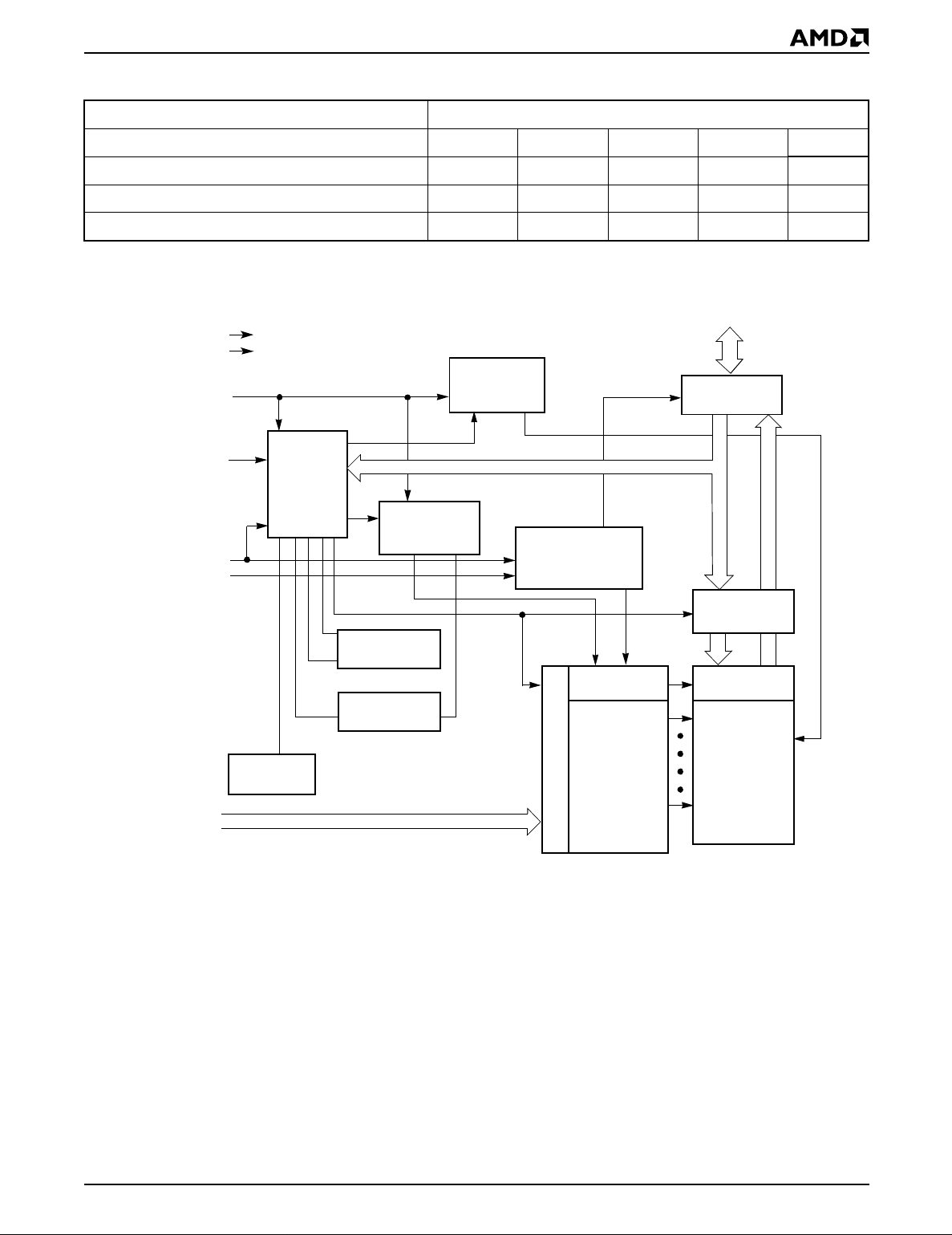
BLOCK DIAGRAM
DQ0–DQ7
V
CC
V
SS
V
PP
WE#
CE#
OE#
State
Control
Command
Re
ister
Program
Volta
Switch
Erase
Voltage
Switch
Input/Output
Buffers
To Array
e
Chip Enable
Output Enable
Logic
A0–A17
Low VCC
Detector
Embedded
Algorithms
Program/Erase
Pulse Timer
Address Latch
Y-Decoder
X-Decoder
Data Latch
Y-Gating
2,097,152
Bit
Cell Matrix
17502D-1
Am28F020A 3
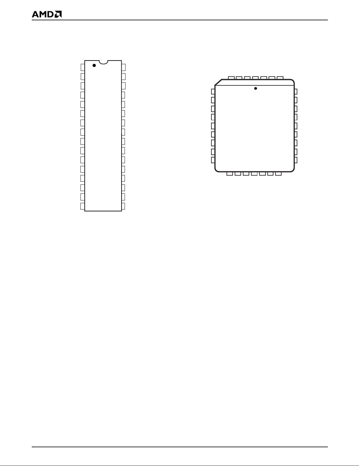
CONNECTION DIAGRAMS
V
PP
A16
A15
A12
A7
A6
A5
A4
A3
A2
A1
A0
DQ0
DQ1
DQ2
V
SS
1
2
3
4
5
6
7
8
9
10
11
12
13
14
15
16
PDIP
32
31
30
29
28
27
26
25
24
23
22
21
20
19
18
17
V
CC
WE# (W#)
A17
A14
A13
A8
A9
A11
OE# (G#)
A10
CE# (E#)
DQ7
DQ6
DQ5
DQ4
DQ3
17502D-2
A7
A6
A5
A4
A3
A2
A1
A0
DQ0
5
6
7
8
9
10
11
12
13
14
A12
4
DQ1
3
15
DQ2
PLCC
A16
A15
2
17
VSS
1
DQ3
VPP
32
18
DQ4
WE# (W#)
VCC
31 30
19 2016
DQ5
A17
29
28
27
26
25
24
23
22
21
DQ6
A14
A13
A8
A9
A11
OE# (G#)
A10
CE# (E#)
DQ7
17502D-3
Note: Pin 1 is marked for orientation.
4 Am28F020A
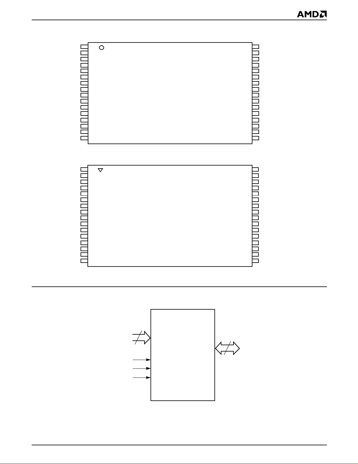
CONNECTION DIAGRAMS (Contin ued)
A11
A9
A8
A13
A14
A17
WE#
V
CC
V
PP
A16
A15
A12
A7
A6
A5
A4
OE#
A10
CE#
D7
D6
D5
D4
D3
V
SS
D2
D1
D0
A0
A1
A2
A3
1
2
3
4
5
6
7
8
9
10
11
12
13
14
15
16
1
2
3
4
5
6
7
8
9
10
11
12
13
14
15
16
32-Pin TSOP—Standard Pinout
32
31
30
29
28
27
26
25
24
23
22
21
20
19
18
17
32
31
30
29
28
27
26
25
24
23
22
21
20
19
18
17
OE#
A10
CE#
D7
D6
D5
D4
D3
V
SS
D2
D1
D0
A0
A1
A2
A3
A11
A9
A8
A13
A14
A17
WE#
V
CC
V
PP
A16
A15
A12
A7
A6
A5
A4
LOGIC SYMBOL
32-Pin TSOP—Reverse Pinout
18
A0–A17
DQ0–DQ7
CE# (E#)
OE# (G#)
WE# (W#)
17502D-4
8
17502D-5
Am28F020A 5
ORDERIN G IN FOR MATION
Standard Products
AMD standard pro ducts are avail able in several packages and operating rang es. The order ing number (Va lid Combinatio n) is
formed by a combination of the following:
AM28F020A -70 J C
DEVICE NUMBER/DESCRIPTION
Am28F020A
2 Megabit (256 K x 8-Bit) CMOS Flash Memory with Embedded Algorithms
B
OPTIONAL PROCESSING
Blank = Standard Processing
B = Burn-In
Contact an AMD representative for more information.
TEMPERATURE RANGE
C = Commercial (0°C to +70°C)
I = Industrial (–40°C to +85°C)
E = Extended (–55°C to +125°C)
PACKAGE TYPE
P = 32-Pin Plastic DIP (PD 032)
J = 32-Pin Rectangular Plastic Leaded Chip
Carrier (PL 032)
E = 32-Pin Thin Small Outline Package (TSOP)
Standard Pinout (TS 032)
F = 32-Pin Thin Small Outline Package (TSOP)
Reverse Pinout (TSR032)
SPEED OPTION
See Product Selector Guide and Valid Combinations
Valid Combinations
AM28F020A-70
AM28F020A-90
AM28F020A-120
AM28F020A-150
AM28F020A-200
PC, PI, PE,
JC, JI, JE,
EC, EI, EE,
FC, FI, FE
Valid Combinations list configurations planned to be supported in volume for this device. Consult the local AMD sales office to confirm availab ility of specific val id combination s and
to check on newly released combinations.
6 Am28F020A
Valid Combinations

PIN DESCRIPTION
A0–A17
Address In puts for memor y lo cations. Inte rnal la tches
hold addresses during write cycles.
CE# (E#)
Chip Enable active low input activates the chip’s control
logic and input buffers. Chip Enable high will deselect
the device and operates the chip in stand-by mode.
DQ0–DQ7
Data Inputs during memory write cycles. Internal
latches hold data during write cycles. Data Outputs
during memory read cycles.
NC
No Conn ect- corre spond ing pin i s no t conn ec ted in ternally to the die.
OE# (G#)
Output Enable active low input gates the outputs of
the device th rough the da ta buffers during me mor y
read cycles. Output Enable is high during command
sequencing and program/erase operations.
V
PP
Program voltage input. VPP must be at hi gh voltag e in
order to write to the command register. The command
register controls all functions required to alter the memory array contents. Memory contents cannot be altered
when VPP ≤ VCC +2 V.
V
CC
Po w er supp ly for de vi ce oper at ion . (5.0 V ± 5% or 10%)
V
SS
Ground.
WE# (W#)
Write Enable active low input controls the write function
of the command register to the memory array. The target address is latched on the falling edge of the Write
Enable pulse and the appropriate data is latched on the
rising edg e of t he pul se. Writ e E nabl e h igh i nhi bit s wri ting to the device.
Am28F020A 7

BASIC PRINCIPLES
The Am28FxxxA family uses 100% TTL-level control
inputs to manage the command regi ster. Erase and
reprogramming op erations use a fixed 12.0 V ± 5%
high voltage input.
Read Only Memory
Without high VPP voltage, the device functions as a
read only memory and operates like a standard
EPROM. Th e control inpu ts still ma nage traditi onal
read, standby, output disable, and Auto select modes.
Command Register
The command register is enabled only when high voltage is applied to the VPP pin. The erase and reprogramming operations are only accessed via the
register. In addition, two-cycle commands are required
for erase and reprogramming op erations. The traditional read, standby, output disable, and Auto select
modes are available via the register.
The device’ s command register is written using standard
microproce ssor wr ite timin gs. The register c ontrols an
interna l state machine that mana ges all device operations. For system design simplification, the device is designed to support either WE# or CE# control led writes.
During a system write cycle, addresses are latched on
the falling edge of WE# or CE# whichever occurs last.
Data is latched on the rising edge of WE# or CE# whichever occur first. To si mplify the following discussion, the
WE# pin is used as t he write cycle control pin throughout
the rest of this text. All setup and hold times are with respect to the WE# signal.
OVERVIEW OF ERASE/PROGRAM OPERATIONS
Embedded
AMD now makes erasure extremely simple and reliable. The Embedded Erase algorithm requires the user
to only write an erase setup command and erase command. The d evice will autom atically pre-pr ogram and
verify the entir e array. The device automatical ly times
the erase pulse width, provides the erase verify and
counts the number of sequences. A status bit, Data#
Polling, provides feedback to the user as to the status
of the erase operation.
Erase Algorithm
Embedded Programming Algorithm
AMD now makes programming extremely simple and
reliable. The Embedded P rogramming algorith m re-
quires the user to on ly writ e a pr ogr am s etu p comma nd
and a program comm and. The device automatically
times the programm ing puls e width, provi des the p rogram verify and counts the number of sequences. A
status bit, Data# Polling, provides feedback to the user
as to the status of the programming operation.
DATA PROTECTION
The device is designed to offer protection aga inst acci dental erasure or programming ca used by spurious
system level signals that may exist during power transitions . The d evice po wers up in it s r ea d onl y st at e . A ls o,
with its control register architecture, alteration of the
memory contents only occurs after successful completion of specific command sequences.
The device al so i ncor pora tes s everal feat ures t o pre vent inadvertent write cycles resulting from V
power-up and power-down transitions or system noise.
CC
Low VCC Write Inhibit
To avoid initiation of a write cycle during VCC power -up
and power-d own, the d evice locks out wr ite cycl es for
VCC < V
ages). When VCC < V
abled, all internal program/erase circuits are disabled,
and the device resets to the read mode. The device ignores all writes until V
that the control pins are in the correct logic state when
VCC > V
(see DC characteristics section for volt-
LKO
to prevent unintentional writes.
LKO
, the command register is dis-
LKO
> V
CC
. The user m ust ensure
LKO
Write Pulse “Glitch” Protection
Noise pulses of less than 10 ns (typical) on OE#, CE#
or WE# will not initiate a write cycle.
Logical Inhibit
Writing is inhibited by holding any one of OE# = VIL,
CE# = VIH or WE# = VIH. To initiate a wri te cycle CE#
and WE# must be a logical zero while OE# is a logical
one.
Power-Up Write Inhibit
Power-up of th e device with W E# = CE # = VIL and
OE# = VIH will not a ccept comman ds on the r ising
edge of WE#. The internal state ma chine is automatically reset to the read mode on power-up.
8 Am28F020A
FUNCTIONAL DESCRIPTION
Description Of User Modes
Table 1. Am28F0 20A Device Bus Operations (Notes 7 and 8)
Read-Only
Read/Write
CE
Operation
(E#)
Read V
Standby V
Output Disable V
Auto-select Manufacturer
Code (Note 2)
Auto-select Device
Code (Note 2)
Read V
Standby (Note 5) V
Output Disable V
Write V
V
V
OE
#
(G#)
IL
IH
IL
IL
IL
IL
IH
IL
IL
V
V
V
V
V
V
V
WE
#
(W#)
IL
XV
XXV
V
IH
IL
IL
IL
IH
V
IH
V
IH
V
IH
XXV
V
IH
IH
IH
V
IL
V
#
PP
(Note 1) A0 A9 I/O
PPL
PPL
V
PPL
V
PPL
V
PPL
V
PPH
PPH
V
PPH
V
PPH
A0 A9 D
X X HIGH Z
X X HIGH Z
V
V
IL
V
IH
ID
(Note 3)
V
ID
(Note 3)
A0 A9
X X HIGH Z
X X HIGH Z
A0 A9
Legend:
X = Don’t care, where Don’t Care is either V
of V
. 0 V < An < VCC + 2 V, (normal TTL or CMOS input levels, where n = 0 or 9).
PPH
or VIH levels. V
IL
= VPP < VCC + 2 V. See DC Characteristics for voltage levels
PPL
Notes:
1. V
may be grounded, connected with a resistor to ground, or < VCC + 2.0 V. V
PPL
the device. Refer to the DC characteristics. When VPP = V
, memory contents can be read but not written or erased.
PPL
is the programming voltage specified for
PPH
2. Manufacturer and device codes may also be accessed via a command register write sequence. Refer to Table 2.
3. 11.5 < V
4. Read operation with V
5. With V
6. Refer to Table 3 for valid D
7. All inputs are Don’t Care unless otherwise stated, where Don’t Care is either V
addresses except A
8. If V
< 13.0 V. Minimum VID rise time and fall time (between 0 and VID voltages) is 500 ns.
ID
= V
PP
at high voltage, the standby current is ICC + IPP (standby).
PP
and A0 must be held at VIL.
9
1.0 Volt, the voltage difference between VPP and VCC should not exceed 10.0 volts. Also, the Am28F256 has a VPP
≤
CC
may access array data or the Auto select codes.
PPH
during a write operation.
IN
or VIH levels. In the Auto select mode all
IL
rise time and fall time specification of 500 ns minimum.
OUT
CODE
(01h)
CODE
(29h)
D
OUT
(Note 4)
D
IN
(Note 6)
Am28F020A 9
READ-ONLY MODE
When VPP is less than V
is inactive. The device can either read array or autoselect data, or be standby mode.
+ 2 V, the comm and regis ter
CC
Read
The device f unc t ion s as a r ea d o nly m em ory wh en V
< V
+ 2 V . The de v ice ha s tw o con tro l fu ncti ons . Bo th
CC
must be satisfied in order to output data. CE# controls
power to the d evice. This pin sh ould be used for specific device selection. OE# controls the device outputs
and shou ld be used to gate data to the output pin s if a
device is selected.
Address access time t
is equal to the delay from
ACC
stable addresses to valid ou tput data. Th e ch i p en able
access time tCE is the delay from stable addresses and
stable CE# to valid data at the output pins. The output
enable access time is the delay from the falling edge of
OE# to valid dat a at the o utp ut pins (assumi n g th e ad dresses have been stable at least t
ACC
- tOE).
PP
Standby Mode
The device has two standby modes. The CMOS
standby mode (CE# input held at V
sumes less than 100 µA of curren t. TTL standby mode
(CE# is held at VIH) reduces the current requirements
to less than 1 m A . When in the stan dby mo de the outputs are in a high impedance state, independent of the
OE# input.
If the device is deselected during eras ure, programming, or p rogram/erase verificati on, the device will
draw active current until the operation is terminated.
± 0.5 V), con-
CC
Output Dis a ble
Output from the device is disabled when OE# is at a
logic high level. When disabled, output pins are in a
high impedance state.
Auto Select
Flash memories can be programmed in-system or in a
standard PROM programmer. The device may be soldered to the circuit board upon receipt of shipment and
programmed in-system. Alternatively, the device may
initially be programmed in a PROM programmer pr ior
to soldering the device to the board.
The Auto se l e ct m od e allows th e r e ad in g ou t of a bin a ry
code from the device that will identify its manufacturer and
type. This mode is intended for the purpose of automatically matching the device to be programmed with its corresponding pr ogramming algorithm . This mode is
functio nal ove r the entir e temperat ure range of the devi ce.
Programming In A PROM Programmer
To activate thi s mode, the programmin g equipm ent
must force VID (11.5 V to 13.0 V ) on addre ss A9 . Two
identi fie r b yte s ma y th en be seq uence d fr om th e de vi ce
outputs by toggling address A0 from VIL to VIH. All other
address lines must be held at VIL, and VPP must be
less than or equal to VCC + 2.0 V while using this Auto
select mode. Byte 0 (A0 = VIL) repr esen ts th e man uf acturer code and byte 1 (A0 = VIH) the device identifier
code. For the device the two bytes are given in the table
2 of the device data sheet. All identifiers for manufacturer and device codes will exhibit o dd parity with th e
MSB (DQ7) defined as the parity bit.
Table 2. (Am28F020A Auto Select Code
Type A0
Manufacturer Code V
Device Code V
10 Am28F020A
Code
(HEX)
IL
IH
01
29
ERASE, PROGRAM, AND READ MODE
When VPP is equal to 12.0 V ± 5%, the command register is active. All fu nctions ar e available. Tha t is, the
device can program, erase, read array or autoselect
data, or be standby mode.
Write Operations
High voltage must be applied to the VPP pin in orde r to
activate the command register. Data written to the register serves as input to the internal state machine. The
output of the state machine determines the operational
function of the device.
The command register does not occupy an addressable memory locat ion. The re giste r is a latch t hat stor es
the com mand , along with th e addr ess and data in formation needed to execute the command. The register
is written by bringing WE# and CE# to VIL, while OE#
is at VIH. Addresses are latched on the falling edge of
WE#, while data is latched on the rising edge of the
WE# pulse. Standard microprocessor write timings are
used.
The device requires the OE# pin to be VIH for write operations. This condition eliminates the possibility for
bus contention during programming operations. In
order to write, OE# must be VIH, and CE# and WE#
must be VIL. If any pin is not in the correct state a write
command will not be executed.
Refer to AC Write Characteristics and the Erase/Programming Waveforms for specific timing parameters.
Command Definitions
The contents of the command register default to 00h
(Read Mode) in the absence of high v oltage appl ied to
the VPP pin. The d evice op erates as a read only
memory. High voltage on the VPP pin enables the
command register. Device operations are selected by
writing specific dat a code s into t he command regi st er .
Table 3 in the de vice d ata sheet defi nes thes e regi ster
commands.
Read Command
Memor y conte nts can be acces sed via th e read com mand when VPP is high. To read from the device, write
00h into the command register. Standard microprocessor read cycles access data from the memory. The device will remain in the read mode until the command
register contents are altered.
The comma nd register defaults to 00h (r ead mode)
upon VPP power -up . The 00h (Rea d Mode ) regis ter default helps ensure that inadvertent alteration of the
memory contents does not occur during the VPP power
transition. Refer to the AC Read Characteristics and
Waveform s for the spec ifi c timi n g para m ete rs.
Table 3. Am28F020A Command Definitions
First Bus Cycle Second Bus Cycle
Operation
Command
Read Memory (Note 4) Write X 00h/FFh Read RA RD
Read Auto select Write X 80h or 90h Read 00h/01h 01h/29h
Embedded Erase Set-up/
Embedded Erase
Embedded Program Set-up/
Embedded Program
Reset (Note 4) Write X 00h/FFh Write X 00h/FFh
Notes:
1. Bus operations are defined in Table 1.
2. RA = Address of the memory location to be read.
PA = Address of the memory location to be programmed.
Addresses are latched on the falling edge of the WE
X = Don’t care.
3. RD = Data read from location RA during read operation.
PD = Data to be programmed at location PA. Data latched on the rising edge of WE
4. Please reference Reset Command section.
(Note 1)
Write X 30h Write X 30h
Write X 10h or 50h Write PA PD
Address
(Note 2)
pulse.
#
Data
(Note 3)
Operation
(Note 1)
.
#
Address
Note 2)
Data
(Note 3)
Am28F020A 11

FLASH MEMORY PROGRAM/ERASE OPERATIONS
Embedded Erase Algorithm
The auto matic chi p erase does no t requ ire the device
to be entirely pre-programmed prior to executing the
Embedded set-up erase command and Embedded
erase command. Upon executing the Embedded erase
command the device automatically will program and
verify the entire memory for an all zero data pattern.
The system is
timing during these operations.
not
required to provide any controls or
has been achieved for the memory array (no erase verify command is required). Th e margin voltages are internally generated in the same manner as when the
standard erase verif y command is used.
The Embedded Erase Set-Up command is a command
only ope ration that s tages the devic e for automatic
electrical erasure of all bytes in the array. Embedded
Erase Setup is performed by writing 30h to the command re gister.
When the device is automatically verified to contain an
all zero patte rn , a self -tim ed ch ip erase and verify begin. The erase and verify operation are complete when
the data on DQ7 is “1" (see Write Operation Status section) atw hich time the device returns to Read mode.
The system is not required to provide any control or
timing during these operations.
When using th e Embedded Erase algorithm, the erase
automatically terminates when adequate erase margin
Apply V
Write Embedded Erase Setup Command
Write Embedded Erase Command
Data# Poll from Device
To commence automatic chip erase, the command 30h
must be written again to the command register. The automatic erase begins on the rising edge of the WE and
terminates when the data on DQ7 is “1" (see Write Operation Status section) at which time the device returns
to Read mode.
Figure 1 and Table 4 illustrate the Embedded Erase algorithm, a typical command string and bus operation.
START
PPH
Erasure Completed
Figure 1. Embedded Erase Algorithm
Table 4. Embedded Erase Algorithm
Bus Operations Command Comments
Standby Wait for V
Write
Read Data
Standby Compare Output to FFh
Read Available for Read Operations
See AC and DC Characteristics for values of V
Note:
switchable. When V
to Functional Description.
Embedded Erase Setup Command Data = 30h
Embedded Erase Command Data = 30h
parameters. The V
is switched, V
PP
may be ground, no connect with a resistor tied to ground, or less than VCC + 2.0 V. Refer
PPL
PP
Ramp to V
PP
Polling to Verify Erasure
#
power supply can be hard-wired to the device or
PP
(see Note)
PPH
12 Am28F020A
17502D-6

Embedded Programming Algorithm
The Embedded Program Setup is a command only operation that st ages the device for autom atic p rogram ming. Embedd ed Program Setup is performed by
writing 10h or 50h to the command register.
Once the Embedded Setup Program operation is performed, the next WE# pulse causes a transition to an
active pro gr amming oper ati on. Addres ses are l atch ed
on the falling edge of CE# or WE# pulse, whichever
happens later. Data is latched on the rising edge of
WE# or CE#, whiche ver hap pens fir st. The rising edge
Apply V
Write Embedded Setup Program Command
Write Embedded
of WE# also begins the programming operation. The
system is not required to provide further controls or
timings. The device will auto matically provide an adequate internally generated program pulse and verify
margin. Th e automatic programmi ng operation is
completed when the dat a on DQ7 is equiv alent to dat a
written to this bit (see Write Operat ion Stat us section)
at which time the device returns to Read mode.
Figure 2 and Table 5 illustrate the Embedded Program
algorithm, a typical command string, and bus operation.
START
PPH
Program Command (A/D)
Data# Poll Device
Increment Address
No
Last Address
Yes
Programming Completed
Figure 2. Embedded Programming Algorithm
Table 5. Embedded Programming Algorithm
Bus Operations Command Comments
Standby Wait for V
Write Embedded Program Setup Command Data = 10h or 50h
Write Embedded Program Command Valid Address/Data
Read Data
Read Available for Read Operations
Ramp to V
PP
Polling to Verify Completion
#
(see Note)
PPH
17502D-7
Note: See AC and DC Characteristics for values of V
switchable. When V
to Functional Description. Device is either powered-down, erase inhibit or program inhibit.
is switched, V
PP
may be ground, no connect with a resistor tied to ground, or less than VCC + 2.0 V. Refer
PPL
parameters. The V
PP
power supply can be hard-wired to the device or
PP
Am28F020A 13

Write Operation Status
Data Polling—DQ7
The device features Data# Polling as a method to indicate to the host system that the Embedded algorithms
are either in progress or completed.
While the Embedded Programming algorithm is in operation, an attempt to read the device at a valid address
will produce the complement of expected Valid data on
DQ7. Upon completion of the Embedded Program algorithm an attempt to read the devi ce at a v alid address will
produce V alid data on D Q7. The Data# P olling f eature i s
valid after the ri sing edge of the secon d WE# pulse of
the two write pulse sequence.
START
While the Embedded Erase algorithm is in operation,
DQ7 will read “0" until the erase operation is completed. Upon completion of the erase operation, the
data on DQ7 will read “1.” The Data# Polling feature is
valid after the rising edge of the second WE# pulse of
the two Write pulse sequence.
The Data# Polling feature is only active during Embedded Programming or erase algorithms.
See Figures 3 and 4 for the Data# Polling timing specifications and diagrams. Data# Polling is the standard
method to check the write operation status, however,
an alternative method is available using Toggle Bit.
No
Read Byte
(DQ0–DQ7)
Addr = VA
DQ7 = Data
?
No
DQ5 = 1
?
Yes
Read Byte
(DQ0–DQ7)
Addr = VA
DQ7 = Data
?
No
VA = Byte address for programming
= XXXXh during chip erase
Yes
Yes
Fail
Note:
DQ7 is rechecked even if DQ5 = “1” because DQ7 may change simultaneously with DQ5 or after DQ5.
Pass
Figure 3. Data# Polling Algorithm
14 Am28F020A
17502D-8

CE#
t
CH
t
t
OE
DF
OE#
t
OEH
WE#
DQ7
t
CE
t
WHWH 3 or 4
DQ7#
DQ0–DQ6 = InvalidDQ0–DQ6
*DQ7 = Valid Data (The device has completed the Embedded operation.)
Figure 4. AC Waveforms for Data# Polling during Embedded Algorithm Operations
*
DQ7 =
Valid Data
t
OH
DQ0–DQ7
Valid Data
High Z
17502D-9
Am28F020A 15

Toggle Bit—DQ6
The device a lso features a “Toggle Bit” as a method t o
indicate to the host system that the Embedded algorithms are either in progress or completed.
Successi ve atte mp ts t o rea d d ata fr om th e d evice at a
valid address, while the Embedded Program algori thm
is in progress, or at any address while the Embedded
Erase algorithm is in progress, will result in DQ 6 toggling between one and zero. Once the Embedded Program or Erase algor ithm is comple ted, DQ6 will sto p
START
toggling to indicate the completi on of either Embedded
operation. Only on the next read cycle will valid data be
obtained. The toggle bit is valid afte r the rising edge of
the fi rst WE # pul se of th e t wo write pu lse s equ ence , u nlike Data# Polling which is valid after the rising edge of
the secon d WE # pu l se. T his featu re a l lows th e us er to
determine if the device is partially through the two write
pulse sequence.
See Figures 5 and 6 for t he Toggle Bit timing specifications and diagrams.
Read Byte
(DQ0–DQ7)
Addr = VA
DQ6 = Toggle
No
Read Byte
(DQ0–DQ7)
Addr = VA
DQ6 = Toggle
VA = Byte address for programming
= XXXXh during chip erase
No
?
Yes
DQ5 = 1
?
Yes
No
?
Yes
Fail
Note:
DQ6 is rechecked even if DQ5 = “1” because DQ6 may stop toggling at the same time as DQ5 changing to “1”.
Pass
Figure 5. Toggle Bit Algorithm
16 Am28F020A
17502D-10

CE#
t
OEH
WE#
OE#
Data
DQ0–DQ7
Note:
*DQ6 stops toggling (The device has completed the Embedded operation.)
DQ6 = DQ6 =
Figure 6. AC Waveforms for Toggle Bit during Embedded Algorithm Operations
*
t
OE
DQ6
Stop Toggling
DQ0–DQ7
Valid
17502D-11
DQ5
Exceeded Timing Limits
DQ5 will indicate if the program or erase time has
exceeded the specified limits. This is a failure condition and the device may not be used again (internal
pulse count exceeded). Under these conditions DQ5
will produce a “1.” The prog ram or era se cycle was not
successfully completed. Data# Polling is the only operating funct ion of the de vi ce under this condition. The
CE# circuit will partially power down the device under
these conditions (to approximately 2 mA). T he OE#
and WE# pins will control the output di sable functions
as described in the Command Definitions table in the
corresponding device data sheet.
Parallel Device Erasure
The Embedded Erase algorithm greatly simplifies parallel device erasure. Since the erase process is internal
to the device, a single erase command can be giv en to
multiple devices concurrently . By implementing a parallel erase al gorithm, total erase time may be minimized.
Note that the Flash memories may erase at different
rates. If this is the case, when a d evice is complete ly
eras ed, use a masking code to prevent further e rasure
(over-erasure). The other devices will continue to erase
until verified. The masking code applied could be the
read command (00h).
Power-Up/Power -Down Seque n ce
The device powers-up in the Read only mode. Power
supply sequencing is not required. Note that if VCC ≤
1.0 Volt, the voltage differen ce betwee n VPP and V
CC
should not exceed 10.0 Volts. Also, the device has a
rise VPP rise time a nd fall time sp ecif icatio n of 500 ns
minimu m.
Reset Command
The Reset comm and initializes the Flash m emor y device to the Read mode. In addition, it also provides the
user with a safe method to abort any device operation
(including program or erase).
The Reset must be written two consecutive times after
the Setup Program command (10h or 50h). This will
reset the device to the Read mode.
Followin g any othe r Fl ash co mman d, w rit e the Rese t
command once to the device. This will safely abort any
previous operation and initialize the device to the Read
mode .
The Setup Program command (10h or 50h) is the only
command that requires a two-sequence reset cycle. The
first Reset command is interpreted as program data.
Howev er , FFh data is considered as n ull data during programming operations (memor y cells are only programmed from a logical “1" to “0") . The secon d Reset
command safely aborts the programming operation and
resets the device to the Read mode.
Memory contents are not altered in any case.
Am28F020A 17

This d etai led i nform ation i s for your refere nce. I t may
prove easier to alw ays issue the Re set comm and two
consecutive times. This eliminates the need to determine if you are in the Setup Program state or not.
In-Sys tem Programming Considerations
Flash mem ories can be pr ogram m ed in -system or in a
standard PROM programmer. The device may be soldered to the circuit board upon receipt of shipment and
programmed in-system. Alternatively, the device may
initiall y be pr ogramme d in a PROM program mer pr ior
to soldering the device to the circuit board.
Auto Select Command
AMD’s Flash memories are designed for use in applications where the local CPU alters memory contents.
In order to correctly program any Flash memories
in-system, manufacturer and device codes must be
accessible while the device resides in the target
system. PROM progr ammers t ypically access the si gnature codes by r aising A9 to a hig h voltag e. How ev er ,
multiplexing high voltage onto address lines is not a
generally desired system design practice.
The device contains an Auto Select operation t o supplement traditional PROM programming methodologies.
The operation is initiated by writing 80h or 90h into the
command register. Following this command, a re ad
cycle address 0000h retriev es the manufacturer code of
01h (AMD). A read cycle from address 00 01h returns
the device code (see the Auto Select Code table of the
corresponding device data sheet). To terminate the operation, it is necessary to write another valid command,
such as Reset (00h or FFh), into the register.
18 Am28F020A

ABSOLUTE MAXIMUM RATINGS
y
Storage T emperature . . . . . . . . . . . . –65°C to +125°C
Ambient Temperature
with Power Applied. . . . . . . . . . . . . . –55°C to +125°C
Voltage with Respect to Ground
All pins except A9 and VPP (Note 1) .–2.0 V to +7.0 V
VCC (Note 1). . . . . . . . . . . . . . . . . . . .–2.0 V to +7.0 V
A9, VPP (Note 2) . . . . . . . . . . . . . . .–2.0 V to +14.0 V
Output Short Circuit Current (Note 3) . . . . . . 200 mA
Notes:
1. Minimum DC voltage on input or I/O pins is –0.5 V . During
voltage transitions, input or I/O pins may overshoot V
–2.0 V for periods of up to 20 ns. Maximum DC voltage on
input or I/O pins is V
input or I/O pins may overshoot to VCC +2.0 V for periods
up to 20 ns.
2. Minimum DC input voltage on pins A9 and V
During voltage transitions, A9 and V
VSS to –2.0 V for periods of up to 20 ns. Maximum DC
input voltage on pin A9 and V
overshoot to 14.0 V for periods up to 20 ns.
3. No more than one output may be shorted to ground at a
time. Duration of the short circuit should not be greater
than one second.
4. Stresses abov e those list ed under “Absol ute Maxim um
Ratings” ma y cause permanent damage to the de vice. This
is a stress r atin g only ; fun ctio nal op era tion of th e de v ice a t
these or any other co nditi ons abov e th ose indi cate d in the
operational sections of this data sheet is not implied.
Exposure of the device to absolute maximum rating
conditions f or ext ended period s ma y aff ect d evi ce relia bility.
+0.5 V . During voltage transitions,
CC
PP
may overshoot
PP
is +13.0 V, which may
PP
to
SS
is –0.5 V.
OPERATING RANGES
Commercial (C) Devices
Ambient Temperature (TA). . . . . . . . . . . .0°C to +70°C
Industrial (I) Devices
Ambient Temperature (TA). . . . . . . . . .–40°C to +85°C
Extended (E) Devices
Ambient Temperature (TA). . . . . . . . .–55°C to +125°C
VCC Supply Voltages
VCC. . . . . . . . . . . . . . . . . . . . . . . . +4.50 V to +5.50 V
VPP Voltages
Read . . . . . . . . . . . . . . . . . . . . . . . . –0.5 V to +12.6 V
Program, Erase, and Verify. . . . . . +11.4 V to +12.6 V
Operating ranges define those limits between which the
functionalit
of the device is guaranteed.
Am28F020A 19

MAXI MUM OVERSHOOT
Maximum Negative Input Overshoot
+0.8 V
–0.5 V
–2.0 V
Maximum Positive Input Overshoot
V
+ 2.0 V
CC
V
+ 0.5 V
CC
2.0 V
20 ns
20 ns
20 ns
20 ns 20 ns
20 ns
17502D-12
Maximum VPP Overshoot
13.5 V
V
+ 0.5 V
CC
17502D-13
20 ns
14.0 V
20 ns 20 ns
17502D-14
20 Am28F020A

DC CHARACTERISTICS over operating range unless otherwise specified
TTL/NMOS Compatible
Parameter
Symbol Parameter Description Test Conditions Min Typ Max Unit
I
LI
I
LO
I
CCS
I
CC1
I
CC2
(Note 4)
I
CC3
(Note 4)
I
PPS
I
PP1
I
PP2
(Note 4)
I
PP3
(Note 4)
V
IL
V
IH
V
OL
Input Leakage Current VCC = VCC Max,
V
= VCC or V
IN
SS
Output Leakage Current VCC = VCC Max,
V
= VCC or V
OUT
SS
VCC Standby Current VCC = VCC Max
CE# = V
V
Active Read Current VCC = VCC Max, CE# = VIL, OE# = V
CC
I
Programming Current CE# = V
V
CC
IH
= 0 mA, at 6 MHz
OUT
IL
0.2 1.0 mA
IH
20 30 mA
20 30 mA
±1.0 µA
±1.0 µA
Programming in Progress
Erase Current CE# = V
V
CC
IL
20 30 mA
Erasure in Progress
VPP Standby Current VPP = V
VPP Read Current VPP = V
= V
V
PP
VPP Programming Current VPP = V
PPL
PPH
PPL
PPH
70 200
10 30 mA
±1.0 µA
µA
±1.0
Programming in Progress
VPP Erase Current VPP = V
PPH
10 30 mA
Erasure in Progress
Input Low Voltage –0.5 0.8 V
Input High Voltage 2.0 VCC + 0.5 V
Output Low Voltage IOL = 5.8 mA
0.45 V
VCC = VCC Min
V
OH1
Output High Voltage IOH = –2.5 mA
2.4 V
VCC = VCC Min
V
I
A9 Auto Select Voltage A9 = V
ID
A9 Auto Select Current A9 = VID Max
ID
ID
11.5 13.0 V
550µA
VCC = VCC Max
V
PPL
VPP during Read-Only
Operations
V
PPH
VPP during Read/Write
Note
: Erase/Program are inhibited when
V
= V
PP
PPL
0.0 VCC +2.0 V
11.4 12.6 V
Operations
V
LKO
Low VCC Lock-out Voltage 3.2 3.7 V
Notes:
1. Caution: the Am28F020A must not be removed from (or inserted into) a socket when V
or VPP is applied. If VCC ≤ 1.0
CC
Volt, the voltage difference between VPP and VCC should not exceed 10.0 Volts. Also, the Am28F020A has a VPP rise time
and fall time specification of 500 ns minimum.
2. I
3. Maximum active power usage is the sum of I
is tested with OE# = VIH to simulate open outputs.
CC1
CC
and I
PP
.
4. Not 100% tested.
Am28F020A 21

DC CHARACTERISTICS
CMOS Compatible
Parameter
Symbol Parameter Description Test Conditions Min Typ Max Unit
I
LI
I
LO
I
CCS
I
CC1
I
CC2
(Note 4)
I
CC3
(Note 4)
I
PPS
I
PP1
I
PP2
(Note 4)
I
PP3
(Note 4)
V
IL
V
IH
V
OL
V
OH1
V
OH2
Input Leakage Current VCC = VCC Max,
V
= VCC or V
IN
SS
Output Leakage Current VCC = VCC Max,
V
= VCC or V
OUT
VCC Standby Current VCC = VCC Max
SS
15 100 mA
±1.0 µA
±1.0 µA
CE# = VCC + 0.5 V
V
Active Read Current VCC = VCC Max, CE# = VIL, OE# = V
CC
Programming Current CE# = V
V
CC
I
= 0 mA, at 6 MHz
OUT
IL
IH
20 30 mA
20 30 mA
Programming in Progress
Erase Current CE# = V
V
CC
IL
20 30 mA
Erasure in Progress
VPP Standby Current VPP = V
VPP Read Current VPP = V
Programming Current VPP = V
V
PP
PPL
PPH
PPH
70 200 µA
10 30 mA
±1.0 µA
Programming in Progress
Erase Current VPP = V
V
PP
PPH
10 30 mA
Erasure in Progress
Input Low Voltage –0.5 0.8 V
Input High Voltage 0.7
V
CC
Output Low Voltage IOL = 5.8 mA
V
= VCC Min
CC
VCC + 0.5 V
0.45 V
Output High Voltage IOH = –2.5 mA, VCC = VCC Min 0.85
V
CC
IOH = –100 µA, VCC = VCC Min VCC
–0.4
V
V
I
A9 Auto Select Voltage A9 = V
ID
A9 Auto Select Current A9 = VID Max
ID
ID
11.5 13.0 V
550µA
VCC = VCC Max
V
PPL
VPP during Read-Only
Operations
V
PPH
VPP during Read/Write
Note
: Erase/Program are inhibited when
VPP = V
PPL
0.0 VCC +2.0 V
11.4 12.6 V
Operations
V
LKO
Low VCC Lock-out Voltage 3.2 3.7 V
Notes:
1. Caution: the Am28F020A must not be removed from (or inserted into) a socket when V
or VPP is applied. If VCC ≤ 1.0
CC
Volt, the voltage difference between VPP and VCC should not exceed 10.0 Volts. Also, the Am28F020A has a VPP rise time
and fall time specification of 500 ns minimum.
2. I
3. Maximum active power usage is the sum of I
is tested with OE# = VIH to simulate open outputs.
CC1
CC
and I
PP
.
4. Not 100% tested.
22 Am28F020A

I
CC
in mA
Active
30
25
20
15
10
°
C
-55
°
C
0
°
C
25
°
C
70
°
C
125
5
0
01 23456789101112
Figure 7. Am28 F0 20 A - Average ICC Active vs. Frequency
TEST CONDITIONS
Device
Under
Test
C
L
Note: Diodes are IN3064 or equivalent
6.2 k
Frequency in MHz
VCC = 5.5 V, Addr essing Pattern = Minmax
Data Pattern = Checkerboard
Table 6. Test Specifications
5.0 V
2.7 k
Ω
Ω
17502D-16
Test Condition -70 All others Un it
Output Load 1 TTL gate
Output Load Capacitance, C
(including jig capacitance)
Input Rise and Fall Times
Input Pulse Levels 0.0–3.0 0.45–2.4 V
Input timing measurement
reference levels
Output timing measurement
reference levels
L
30 100 pF
10 ns
≤
1.5 0.8, 2.0 V
1.5 0.8, 2.0 V
17502D-15
Figure 8. Test Setup
Am28F020A 23

SWITCHING TEST WAVEFORMS
s
2.4 V
0.45 V
2.0 V
Test Points
Input Output
2.0 V
0.8 V0.8 V
AC Testing (all speed options except -70): Inputs are driven at
2.4 V for a logic “1” and 0.45 V for a logic “0”. Input pulse rise
and fall times are
10 ns.
≤
3 V
1.5 V
0 V
Input Output
Test Points
1.5 V
AC Testing for -70 devices: Inputs are driven at 3.0 V for a
logic “1” and 0 V for a logic “0”. Input pulse rise and fall time
are ≤10 ns.
17502D-17
SWITCHING CHARACTERISTICS over operating range, unless otherwise specified
AC Character istics—Read-Only Operations
Parameter
Symbols Am28F020A Speed Options
JEDEC Standard Parameter Description -70 -90 -120 -150 -200 Unit
t
AVAV
t
ELQV
t
AVQV
t
GLQVtOE
t
ELQX
t
RC
t
CE
t
ACC
t
LZ
Read Cycle Time (Note 3) Min 70 90 120 150 200 ns
Chip Enable Access Time Max 70 90 120 150 200 ns
Address Access Time Max 70 90 120 150 200 ns
Output Enable Access Time Max 35 35 50 55 55 ns
Chip Enable to Output in Low Z
(2)
Min00000ns
t
EHQZtDF
t
GLQXtOLZ
t
GHQZtDF
t
AXQXtOH
t
VCS
Chip Disable to Output in High Z
(1)
Output Enable to Output in Low Z (2) Min 00000ns
Output Disable to Output in High Z (2) Max 20 20 30 35 35 ns
Output Hold Time From First Address, CE#,
or OE# change (2)
VCC Set-up Time to Valid Read (2) Min 50 50 50 50 50 ns
Notes:
1. Guaranteed by design; not tested.
2. Not 100% tested
24 Am28F020A
Max2020303535ns
Min00000ns

AC Character istics—Write (Erase/Program) Operations
Parameter Symbols Am28F020A Speed Options
JEDEC Standard Description -70 -90 -120 -150 -200 Unit
t
AVAV
t
AVWLtAS
t
WLAXtAH
t
DVWHtDS
t
WHDXtDH
t
OEH
t
GHWL
t
ELWLEtCSE
t
WHEHtCH
t
WLWHtWP
t
WHWLtWPH
t
WHWH3
t
WHWH4
t
VPEL
t
VCS
t
VPPR
t
VPPF
t
LKO
t
WC
Write Cycle Time (4) Min 70 90 120 150 200 ns
Address Setup Time Min 0 0 0 0 0 ns
Address Hold Time Min 45 45 50 60 75 ns
Data Setup Time Min 45 45 50 50 50 ns
Data Hold Time Min 10 10 10 10 10 ns
Output Enable Hold Time for Embedded
Algorithm only
Min 10 10 10 10 10 ns
Read Recovery Time Before Write Min 0 0 0 0 0 ns
CE# Embedded Algorithm Setup Time Min 20 20 20 20 20 ns
CE# Hold Time Min 0 0 0 0 0 ns
Write Pulse Width Min 45 45 50 60 60 ns
Write Pulse Width High Min 20 20 20 20 20 ns
Embedded Program Operation (2) Min 14 14 14 14 14 µs
Embedded Erase Operation (3) Typ 5 5 5 5 5 sec
VPP Setup Time to Chip Enable Low (4) Min 100 100 100 100 100 ns
VCC Setup Time (4) Min 50 50 50 50 50 µs
VPP Rise Time (4) 90% V
VPP Fall Time (4) 90% V
VCC < V
to Reset (4) Min 100 100 100 100 100 ns
LKO
PPH
PPL
Min 500 500 500 500 500 ns
Min 500 500 500 500 500 ns
Notes:
1. Read timing characteristics during read/write operations are the same as during read-only operations. Refer to AC
Characteristics for Read Only operations.
2. Embedded Program Operation of 14 µs consists of 10 µs program pulse and 4 µs write recovery before read. This is the
minimum time for one pass through the programming algorithm.
3. Embedded Erase operation of 5 sec consists of 4 sec array pre-programming time and one sec array erase time. This is a
typical time for one embedded erase operation.
4. Not 100% tested.
Am28F020A 25

KEY TO SWITCHING WAVEFORMS
WAVEFORM INPUTS OUTPUTS
Don’t Care, Any Change Permitted Changing, State Unknown
Does Not Apply Center Line is High Impedance State (High Z)
SWITCHING WAVEFORMS
Steady
Changing from H to L
Changing from L to H
Addresses
CE# (E#)
OE# (G#)
WE# (W#)
Data (DQ)
5.0 V
V
CC
0 V
Power-up, Standby
t
VCS
High Z High Z
Device and
Address Selection
Addresses Stable
t
WHGL
t
GLQV
t
(tCE)
ELQV
t
(tLZ)
ELQX
t
VCS
t
(t
AVQV
ACC
)
Outputs
Enabled
t
AVAV
(tOE)
t
GLQX
(tRC)
(t
OLZ
Data
Valid
)
Output Valid
t
AXQX (tOH
Standby, Power-down
t
EHQZ
(t
)
DF
t
GHQZ
(t
)
DF
)
Figure 9. AC W avefo rms for Read Operations
26 Am28F020A
17502D-18

SWITCHING WAVEFORMS
Addresses
CE#
OE#
WE#
Data
V
CC
t
GHWL
t
t
VCS
CSE
Embedded
Erase Setup
t
WC
t
WP
t
DS
30h
Embedded
Erase Erase Standby
t
AS
t
AH
t
WHWH3 OR 4
t
WPH
t
DH
30h
Data# Polling
DQ7#
DQ7#
Read
t
RC
t
t
DF
OH
t
OE
t
CE
V
PP
t
VPEL
Note:
#
is the complement of the data written to the device.
DQ7
Figure 10. AC Waveforms for Embedded Erase Operatio n
17502D-19
Am28F020A 27

SWITCHING WAVEFORMS
Addresses
CE#
OE#
WE#
Data
V
CC
Embedded
Program Setup
t
t
VCS
t
CSE
WC
t
WP
t
t
DH
DS
t
GHWL
50h
Embedded
t
WPH
Program
PA
t
AS
t
AH
D
IN
t
WHWH3 OR 4
Data# Polling
PA
DQ7#
DQ7# D
OUT
Read
t
RC
t
t
DF
OH
t
OE
t
CE
V
PP
Notes:
is data input to the device.
1. D
IN
2. DQ7
3. D
#
is the complement of the data written to the device.
is the data written to the device.
OUT
t
VPEL
Figure 11. AC Waveforms for Embedded Programming Operation
17502D-20
28 Am28F020A

AC CHARACTERISTICS—WRITE (ERASE/PROGRAM) OPERATIONS
Alternate CE# Controlled Writes
Parameter Symbols Am28F020A Speed Options
JEDEC Standard Description -70 -90 -120 -150 -200 Unit
t
AVAV
t
AVEL
t
ELAXtAH
t
DVEHtDS
t
EHDXtDH
t
OEH
t
GHEL
t
WLELtWS
t
EHWKtWH
t
ELEHtCP
t
EHELtCPH
t
EHEH3
t
EHEH4
t
VPEL
t
VCS
t
VPPR
t
VPPF
t
LKO
t
t
WC
AS
Write Cycle Time (4) Min 70 90 120 150 200 ns
Address Setup Time Min 0 0 0 0 0 ns
Address Hold Time Min 45 45 50 60 75 ns
Data Setup Time Min 45 45 50 50 50 ns
Data Hold Time Min 10 10 10 10 10 ns
Output Enable Hold Time for Embedded
Algorithm only
Min 10 10 10 10 10 ns
Read Recovery Time Before Write Min 0 0 0 0 0 ns
WE# Setup Time by CE# Min 0 0 0 0 0 ns
WE# Hold Time Min 0 0 0 0 0 ns
Write Pulse Width Min 65 65 70 80 80 ns
Write Pulse Width High Min 20 20 20 20 20 ns
Embedded Program Operation (2) Min 14 14 14 14 14 µs
Embedded Erase Operation (3) Typ 5 5 5 5 5 sec
VPP Setup Time to Chip Enable Low (4) Min 100 100 100 100 100 ns
VCC Setup Time (4) Min 50 50 50 50 50 µs
VPP Rise Time (4) 90% V
VPP Fall Time (4) 90% V
VCC < V
to Reset (4) Min 100 100 100 100 100 ns
LKO
PPH
PPL
Min 500 500 500 500 500 ns
Min 500 500 500 500 500 ns
Notes:
1. Read timing characteristics during read/write operations are the same as during read-only operations. Refer to AC
Characteristics for Read Only operations.
2. Embedded Program Operation of 14 µs consists of 10 µs program pulse and 4 µs write recovery before read. This is the
minimum time for one pass through the programming algorithm.
3. Embedded erase operation of 5 sec consists of 4 sec array pre-programming time and one sec array erase time. This is a
typical time for one embedded erase operation.
4. Not 100% tested.
Am28F020A 29

SWITCHING WAVEFORMS
Addresses
WE#
OE#
CE#
Data
V
CC
t
WS
t
GHEL
Embedded
Program Setup
t
WC
t
CP
50h
t
DS
Embedded
Program
t
CPH
Data# Polling
DQ7#
PA
DQ7#
D
OUT
PA
t
AS
t
AH
t
EHEH3 OR 4
t
DH
D
IN
V
PP
t
VPEL
Notes:
is data input to the device.
1. D
IN
#
2. DQ7
3. D
is the complement of the data written to the device.
is the data written to the device.
OUT
Figure 12. AC Waveforms for Embedded Programming Operatio n Using CE# Controlled Writes
17502D-21
30 Am28F020A

ERASE AND PROGRAMMING PERF ORMANCE
Limits
Typ
Parameter
Chip Erase Time 1 10 sec Excludes 00h programming prior to erasure
Chip Programming Time 4 25 sec Excludes system-level overhead
Write/Erase Cycles 100,000 Cycles
Byte Programming Time 14 µs
(Note 1)
Max
(Note 2) Unit
96
(Note 3)
ms
CommentsMin
Notes:
C, 12 V VPP .
1. 25
°
2. Maximum time specified is lower than worst case. Worst case is derived from the Embedded Algorithm internal counter which
allows for a maximum 6000 pulses for both program and erase operations. Typical worst case for program and erase is
significantly less than the actual device limit.
3. Typical worst case = 84 µs. DQ5 = “1” only after a byte takes longer than 96 ms to program.
LATCHUP CHARACTERISTICS
Parameter Min Max
Input Voltage with respect to V
Input Voltage with respect to V
Current –100 mA +100 mA
on all pins except I/O pins (Including A9 and VPP) –1.0 V 13.5 V
SS
on all pins I/O pins –1.0 V VCC + 1.0 V
SS
Includes all pins except V
. Test conditions: VCC = 5.0 V, one pin at a time.
CC
PIN CAPACITANCE
Parameter
Symbol Parameter Description Test Conditions Typ Max Unit
C
IN
C
OUT
C
IN2
Note: Sampled, not 100% tested. Test conditions T
Input Capacitance VIN = 0 8 10 pF
Output Capacitance V
VPP Input Capacitance VPP = 0 8 12 pF
= 25°C, f = 1.0 MHz.
A
= 0 8 12 pF
OUT
DATA RETENTION
Parameter Test Conditions Min Unit
Minimum Pattern Data Retention Time
150°C10Years
125°C20Years
Am28F020A 31

PHYSICAL DIMENSIONS
PD032—32-Pin Plastic DIP (measured in inches)
1.640
1.670
.120
.160
32
.140
.225
Pin 1 I.D.
.045
.065
.005 MIN
.090
.110
.016
.022
17
.530
.580
16
0°
10°
SEATING PLANE
.015
.060
PL032—32-Pin Plastic Leaded Chip Carrier (measured in inches)
.485
.495
.009
.015
.125
.140
.080
.095
SEATING
PLANE
.013
.021
.050 REF.
SIDE VIEW
.585
.595
.447
.453
Pin 1 I.D.
.547
.553
.026
.032
TOP VIEW
.600
.625
.009
.015
.630
.700
16-038-S_AG
PD 032
EC75
5-28-97 lv
.042
.056
.400
REF.
.490
.530
16-038FPO-5
PL 032
DA79
6-28-94 ae
32 Am28F020A

PHYSICAL DIMENSIONS
TS032—32-Pin Standard Thin Small Outline Package (measured in millimeters)
0.95
1.05
Pin 1 I.D.
1
7.90
8.10
0.50 BSC
1.20
MAX
18.30
18.50
19.80
20.20
0.05
0.15
0.08
0.20
0.10
0°
5°
0.50
0.70
0.21
16-038-TSOP-2
TS 032
DA95
3-25-97 lv
Am28F020A 33

PHYSICAL DIMENSIONS
TSR032—32-Pin Reversed Thin Small Outline Package (measured in millimeters)
0.95
1.05
Pin 1 I.D.
1
7.90
8.10
0.50 BSC
1.20
MAX
18.30
18.50
19.80
20.20
0.05
0.15
0.08
0.20
0.10
0°
5°
0.50
0.70
0.21
16-038-TSOP-2
TSR032
DA95
3-25-97 lv
34 Am28F020A

DATA SHEET REVISION SUMMARY FOR AM28F020A
Revision C+1
Distinctive Characteristics:
High Performan ce:
is now 70 ns.
General Description:
Paragraph 2: Changed fastest speed option to 70 ns.
Product Selector Guide:
Added -70, deleted -95 and -250 speed options.
Ordering Information, Standard Products:
The -70 speed option is now listed in the example.
Valid Combinations:
combinations.
Erase, Program, and Read Mode:
Corrected the subheading to read “VPP = 12.0 V ± 5%”.
Operating Ranges:
VCC Suppl y Voltages:
speed options.
The fastest spee d option available
Added -7 0, de leted -95 and -25 0
Added -70, deleted -95 and -250
AC Characte ris ti cs :
Read Only Operations Characteri stics:
column and test conditi ons.
Deleted -95 and -250 speed options.
AC Characte ris ti cs :
Added the -7 0
Writ e/Erase /Program O perati ons, Alter nate CE# Controlled Writes:
-250 speed options.
Switching Test Waveforms:
In the 3.0 V waveform caption, changed -95 to -70.
Added th e -70 column. D elet ed -95 and
Revision D
Matched formatting to other current data sheets.
Revision D+1
Programming In A PROM Progra mmer:
Deleted the paragraph “(Refer to the AUTO SELECT
paragraph in the ER ASE, PROGRAM, and READ
MODE section for programming the Flash memory device in-system).”
Trademarks
Copyright © 1998 Advanced Micro Devices, Inc. All rights reserved.
ExpressFlash is a trademark of Advanced Micro Devices, Inc.
AMD, the AMD logo, and combinations thereof are registered trademarks of Advanced Micro Devices, Inc.
Product names used in this publication are for identification purposes only and may be trademarks of their respective companies.
Am28F020A 35
 Loading...