

Datasheet AM28F010-70PC, AM28F010-70JIB, AM28F010-70JI, AM28F010-70JEB, AM28F010-70JE Datasheet (AMD Advanced Micro Devices)
...
FINAL
Am28F010
1 Megab it (128 K x 8-B it)
CMOS 12.0 Volt, Bulk Erase Flash Memory
DISTINCTIVE CHARACTERISTICS
High performance
■
— 70 ns maximum access time
CMOS Low power consumption
■
— 30 mA maximum active current
— 100 µA maximum standby current
— No data retention power consumption
Compatible with JEDEC-standard byte-wide
■
32-Pin EPROM pinouts
— 32-pin PDIP
— 32-pin PLCC
— 32-pin TSOP
10,000 write/erase cycles minimum
■
Write and erase voltage 12.0 V ±5%
■
Latch-up protected to 100 mA
■
from –1 V to V
CC
+1 V
■
■
■
■
■
■
Flasherase™
Electrical Bulk Chip-Erase
— One second typical chip-erase
Flashrite™ Programming
— 10 µs typical byte-program
— Two seconds typical chip program
Command register architecture for
microprocessor/microcontroller compatible
write interface
On-chip address and data latches
Advanced CMOS flash memory technology
— Low cost single transistor memory cell
Automatic write/erase pulse stop timer
GENERAL DESCRIPTION
The Am28F010 is a 1 Megabit Flash memory organized as 128 Kbytes of 8 bits each. AMD’s Flash memories offer the most cost-effective and reliable read/
write non-volatile random access memory. The
Am28F010 is packaged in 32-pin PDIP, PLCC, and
TSOP versions. It is designed to be reprogrammed
and erased in -system or in standard EPROM programmers. The Am28F010 is erased when shipped
from the factory.
The standard Am28F010 offers acc ess times as f ast as
70 ns, allowing operation of high-speed microprocessors without wait states. To eliminate bus contention,
the Am28F010 has separate chip enable (CE#) and
output enable (OE#) controls.
AMD’s Flash memories augment EPROM functionality
with in-circuit electrical erasure and programming. The
Am28F010 uses a comman d register to manage t his
functionality, while maintainin g a JEDEC Fla sh Standard 32-pin p inout. The command r egister allows for
100% TTL level control inputs and fixed power supply
levels during erase and programming, while maintaining maximum EPROM compatibility.
AMD’s Flash technology reliably stores memory co ntents ev en after 10,000 erase and pr og r am cycl es . The
AMD cell is d esigned t o optimize the erase and programming mechanis ms. In additi on, the com bination of
advanced tunnel oxide processing and low internal
electr ic fields for era se and p rogramming o peration s
produc es reliable cycling. Th e Am28F010 uses a
12.0 V±5% V
Flasherase
high voltage input to perform the
PP
and Flashrite algorithms.
The highest degree of latch-up protection is achieved
with AMD’s proprietary non-epi process. Latch-up protection is provided for stresses up to 100 milliamps on
address and data pins from –1 V to V
CC
+1 V.
The Am28F010 is byte prog rammab le using 10 ms programming pulses in accordance with AMD’s Flashrite
programming algorithm. The typical room temperature
programming tim e of the Am 28F010 is t wo seconds.
The entire chip i s bulk erased usi ng 10 ms erase pulses
according to AMD’s Flasherase alrogithm. Typical erasure at room temperature is accomplished in less than
one second. The windowed package and the 15–20
Publicatio n#
Issue Date:
Rev: HAmendm ent/
11559
January 1998
+2
minutes required for EPROM erasure using ultra-violet
light are eliminated.
Commands are written to the command register using
standard mi cro proces sor wr i te ti ming s. Re gist er contents serve as inputs to an inter nal state-mac hine
which controls the erase and programming circuitry.
During write cycles, the comman d register inter nally
latches address and data needed for the programming
and erase o peration s. For system desi gn simplif ication, the Am28F010 is designed to support either WE#
or CE# controlle d writes. During a system write cycle,
addresses are la tched on the falling edg e of WE# or
CE# whichever occurs last. Data is latched on the ris-
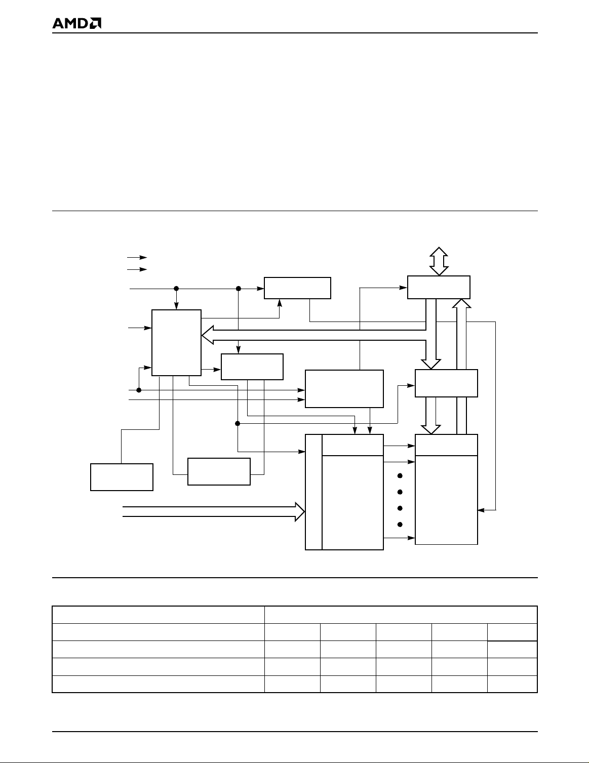
BLOCK DIAGRAM
V
CC
V
SS
V
PP
Erase Voltage
ing edge of WE# or CE# whichever occurs first. To
simplify the following discussion, the WE# pin is used
as the write cycle control pin throughout the rest of
this text. All se tup an d hold times are w ith res pect to
the WE# signal.
AMD’s Flash technology combines years of EPROM
and EEPROM ex perience to produce the highest le vels
of quality, reliability, and cost effectiveness. The
Am28F0 10 electri cally eras es all bits simultane ously
using Fowler-Nordheim tunneling. The bytes are programmed one byte at a time using the EPROM programming mechanism of hot electron injection.
DQ0–DQ7
Input/Output
Switch
Buffers
WE
CE
OE
Low V
Detector
A0–A16
#
#
#
CC
State
Control
Command
Register
Program/Erase
Pulse Timer
PRODUCT SELECTOR GUIDE
Program
Voltage Switch
To Array
Chip Enable
Output Enable
Logic
Y-Decoder
X-Decoder
Address Latch
Data
Latch
Y-Gating
1,048,576 Bit
Cell Matrix
11559H-1
Family Part Number
Speed Options (V
Max Access Time (ns) 70 90 120 150 200
(E#) Access (ns) 70 90 120 150 200
CE
#
(G#) Access (ns) 35 35 50 55 55
OE
#
= 5.0 V ± 10%)
CC
-70 -90 -120 -150 -200
Am28F010
2 Am28F010
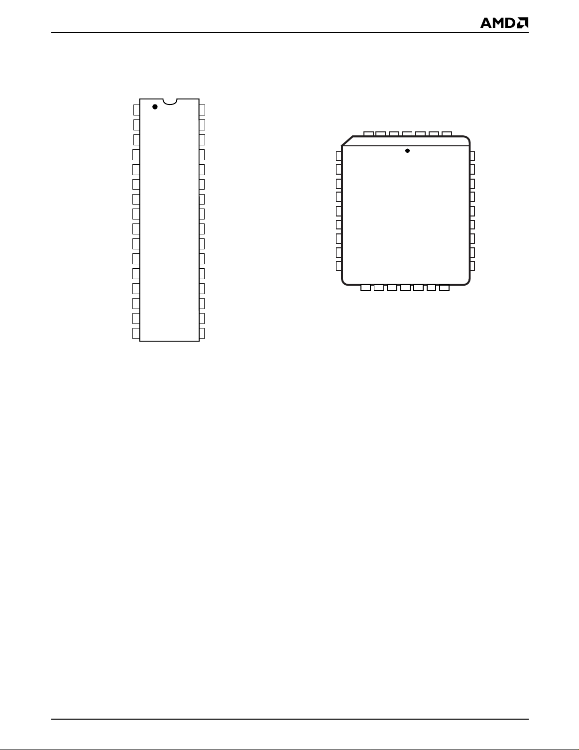
CONNECTION DIAGRAMS
V
PP
A16
A15
A12
A7
A6
A5
A4
A3
A2
A1
A0
DQ0
DQ1
DQ2
V
SS
1
2
3
4
5
6
7
8
9
10
11
12
13
14
15
16
PDIP
32
31
30
29
28
27
26
25
24
23
22
21
20
19
18
17
V
CC
WE# (W#)
NC
A14
A13
A8
A9
A11
OE# (G#)
A10
CE# (E#)
DQ7
DQ6
DQ5
DQ4
DQ3
A7
A6
A5
A4
A3
A2
A1
A0
DQ0
5
6
7
8
9
10
11
12
13
14
A12
4
DQ1
15
A15
3
DQ2
PLCC
A16
2
17
SS
V
NC
VCCWE# (W#)
31 30
1
32
19 2016
18
DQ4
DQ3
DQ5
NC
29
28
27
26
25
24
23
22
21
DQ6
A14
A13
A8
A9
A11
OE# (G#)
A10
CE# (E#)
DQ7
Note: Pin 1 is marked for orientation.
11559H-2
11559H-3
Am28F010 3
CONNECTION DIAGRAMS (continued)
A9
A8
CC
A7
A6
A5
A4
SS
1
2
3
4
5
6
7
#
8
9
10
11
12
13
14
15
16
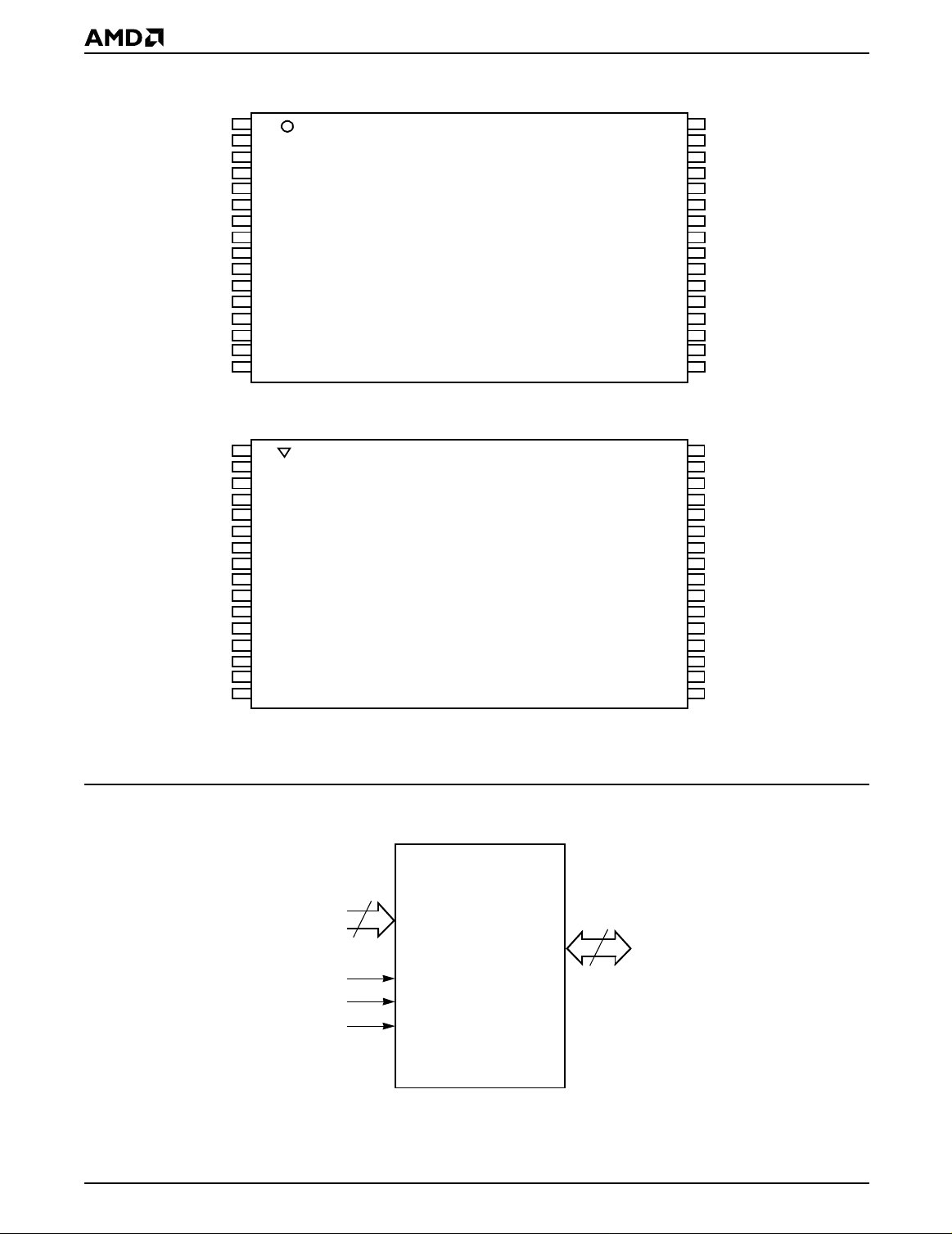
32-Pin TSOP—Sta ndard Pinout
#
1
2
#
3
4
5
6
7
8
9
10
11
12
13
14
15
16
A11
A13
A14
NC
WE
V
NC
A16
A15
A12
OE
A10
CE
D7
D6
D5
D4
D3
V
D2
D1
D0
A0
A1
A2
A3
TSOP
32
31
30
29
28
27
26
25
24
23
22
21
20
19
18
17
32
31
30
29
28
27
26
25
24
23
22
21
20
19
18
17
OE
A10
CE
D7
D6
D5
D4
D3
V
SS
D2
D1
D0
A0
A1
A2
A3
A11
A9
A8
A13
A14
NC
WE
V
CC
NC
A16
A15
A12
A7
A6
A5
A4
#
#
#
32-Pin TSOP—Reverse Pinout
LOGIC SYMBOL
17
A0–A16
DQ0–DQ7
CE
(E#)
#
OE# (G#)
WE# (W#)
4 Am28F010
11559H-4
8
11559H-5
ORDERING INFORMATION
Standard Products
AMD standard pro ducts are av ailab le i n several packages and op erating r ange s. The or der n umber (Valid Combination) is f ormed
by a combination of:
AM28F010 -70 J C
DEVICE NUMBER/DESCRIPTION
Am28F010
1 Megabit (128 K x 8-Bit) CMOS Flash Memory
B
OPTIONAL PROCESSING
Blank = Standard Processing
B=Burn-In
Contact an AMD representative for more information.
TEMP ERATURE RANGE
C = Commercial (0°C to +70°C)
I = Industrial (–40°C to +85°C)
E = Extended (–55°C to +125°C)
PACKA GE TYPE
P = 32-Pin Plastic DIP (PD 032)
J = 32-Pin Rectangular Plastic Leaded Chip
Carrier (PL 032)
E = 32-Pin Thin Small Outline Package (TSOP)
Standard Pinout (TS 032)
F = 32-Pin Thin Small Outline Package (TSOP)
Reverse Pinout (TSR032)
SPEED OPTION
See Product Selector Guide and Valid Combinations
AM28F010-70
AM28F010-90
AM28F010-120
AM28F010-150
AM28F010-200
Valid Combinations
PC, PI, PE,
JC, JI, JE,
EC, EI, EE,
FC, FI, FE
Valid Combinations
Valid Combinations list configurations planned to be supported in volume for this device. Consult the local AMD sales
office to confirm availability of specific valid combinations and
to check on newly released combinations.
Am28F010 5

PIN DESCRIPTION
A0–A16
A
ddress Inputs for memory locations. Internal latches
hold addresses during write cycles.
CE# (E#)
Chip Enable active low input activates the chip’s control logic and input buffers. Chip Enable high will deselect the device and operates the chip in stand-by mode.
DQ0–DQ7
Data Inputs during memory write cycles. Internal
latches hold data during write cycles. Data Outputs
during memory read cycles.
NC
No Connect-co rresponding pin is not connecte d
internally to the die.
OE# (G#)
Output Enable active lo w input gates the outputs of the
device through the data buffers dur ing memo ry rea d
cycles. Output Enable is high during command
sequencing and program/erase operations.
V
CC
Po wer supply f or de vice operation. (5.0 V ± 5% or 10%)
V
PP
Program voltage input. VPP must be at high voltage in
order to write to the command register. The command
register controls all functions required to alter the memory array contents . Memory contents cannot be alter ed
≤ V
when V
V
SS
Ground
PP
CC
+2 V.
WE# (W#)
Write Enable active l ow input controls the write function
of the command register to the memory array. The target address is latched on the falling edge of the Write
Enable pulse and the appropriate data is la tched on the
rising edge of the pulse. Write E nable high inhibits
writing to the device.
6 Am28F010

BASIC PRINCIPLES
The device use s 100% TTL-l evel control inputs to
manage the command register. Erase and reprogramming operations use a fixed 12.0 V ± 5% high
voltage input.
Read Only Memory
Without high VPP voltage, the device functions as a
read only memor y and operate s like a standar d
EPROM. The control inputs still manage traditional
read, standby, output disable, and Auto select modes.
Command Register
The command register is enabled only when high voltage is applied to the V
gramming operat ions are only acce ssed via the
register. In addition, two-cycle commands are required
for erase and reprogramming operations. The traditional read, standby, output disable, and Auto select
modes are available via the register.
The device’s command register is writ ten using standard microp rocessor w rite timin gs. The re gister controls an internal state machine that manages all device
operations. For syst em desig n simplificat ion, the de vice is designed to support either WE# or CE# controlled writes. During a system write cycle, addresses
are latched on the falling edge of WE# or CE# whichever occurs last. Data is latched on the rising edge of
WE# or CE# whichever occur first. To simplify the following discussion, the WE# pin is used as the write
cycle control pin throughout the rest of this text. All
setup and hold times are with respect to the WE# signal.
pin. The erase and repro-
PP
Overview of Er as e/Progr am Ope ra ti on s
Flasherase™ Sequence
A multiple step command seq uence is require d to
erase the Flash device (a two-cyc le Erase command
and repeated one cycle verify commands).
Note: The Flash memory array must be completely
programmed to 0’s prior to erasure. Refer to the
Flashrite™ Programming Algorithm.
1. Erase Setup: Write the Setup Erase command to
the command register.
2. Erase: Write the Erase command (same as Setup
Erase comman d) to t he comman d register again.
The second command initiates the er ase operation.
The system software routine s must now time-ou t
the erase pulse wid th (10 ms) prior t o issuing the
Erase-verify command. An integrated stop timer
prevents any possibility of overerasure.
3. Erase-Verify: Wr ite the Erase-verify command to
the command register. This command terminates
the erase ope ration. After the erase op eration,
each byte of the array must be verified. Address in-
formation must be supplied with the Erase-verify
command. This command verifies the mar gin and
outputs the addressed byte in order to compare the
array data with FFh data (Byte erased).
After successful data verification the Erase-verify
command is written again with new address information. Each byte of t he a rray is sequentially verified in this manner.
If data of the addressed location is not verified, the
Erase sequence is repeated until the entire array is
successfully verified or the sequence is repeated
1000 times.
Flashrite
A three step command sequence (a two- cycle Progr am
command and one cycle Verify command) is required
to program a byte of the Flash arra y. Refer to the Flashrite
1. Program Setup: Write the Setup Program com-
2. Program: Write the Program command to the com-
3. Program-Verify: Write the Program-verify com-
If data is not verified successfully, the Program sequence is repeat ed until a success ful comp arison is
verified or the sequence is repeated 25 times.
Programming Sequence
Algorithm.
mand to the command register.
mand register with the appropriate Address and
Data. The system software routines m ust no w timeout the program pulse width (10 µs) prior to issuing
the Progr am-verify co mmand. An in tegrated sto p
timer prevents any possibility of overprogramming.
mand to the command register. This command terminates the programming operation. In addition,
this command verifies the margin and ou tputs the
byte just progr ammed in or der to compare the arr a y
data with the original data programmed. After successful data verification, the programming sequence is initiated again f or the ne xt b yte address to
be programmed.
Data Protection
The device is designed to off er protection against accidental erasure or programming caused by spurious
system lev el signals that ma y exist during power transitions. The de vic e power s up i n its read only s tate. A lso,
with its co ntrol reg ister ar chitectu re, alteration of the
memory contents only occurs after successful completion of specific command sequences.
The device also incorporates several features to prevent inadv ertent write cycles resulting fromV
up and power-down transitions or system noise.
power-
CC
Low VCC Write Inhibit
To avoid initiation of a write cycle during VCC power-up
and power-down, the device locks out write cycles for
Am28F010 7
VCC < V
voltages). When V
disabled, al l internal pro gram/erase circuits are
disabled, and the device resets to the read mode. The
device ignores all writes until V
must ensure that the control pins are in the correct logic
state when V
Write Pulse “Glitch” Protection
Noise pulses of less than 10 ns (typical) on OE#, CE#
or WE# will not initiate a write cycle.
(see DC C haracteristics section for
LKO
CC
> V
CC
< V
LKO
, the command register is
LKO
> V
CC
to prev ent uni nitentional writes.
LKO
. The user
Logical Inhibit
Writing i s inhibi ted by holding any one of OE# = VIL, CE#
or WE# = VIH. To initiate a write cycle CE# and
= V
IH
WE# must be a logical zero while OE# is a logical one.
Power-Up Write Inhibit
Power-up of the device with WE# = CE# = VIL and
OE# = V
edge of WE # . The in te rn al st at e ma chine is a ut oma tically reset to the read mode on power-up.
will not accept commands on the rising
IH
FUNCTIONAL DESCRIPTION
Description of User Modes
Table 1. Am28F010 Device Bus Operations
Operation CE# (E#)OE# (G#)WE# (W#)
V
PP
(Note 1) A0 A9 I/O
Read-Only
Read/Write
Read V
Standby V
Outp ut Disable V
Auto-Select Manufacturer
Code (Note 2)
Auto-Select Device Code
(Note 2)
Read V
Standby (Note 5) V
Outp ut Disable V
Write V
IL
IH
IL
V
IL
V
IL
IL
IH
IL
IL
V
IL
XXV
V
IH
V
IL
V
IL
V
IL
XXV
V
IH
V
IH
XV
V
IH
V
IH
V
IH
V
IH
V
IH
V
IL
V
V
V
V
V
V
PPL
PPL
PPL
PPL
PPL
PPH
PPH
PPH
PPH
A0 A9 D
XXHIGH Z
XXHIGH Z
V
IL
V
IH
VID
(Note 3)
VID
(Note 3)
A0 A9
XXHIGH Z
XXHIGH Z
A0 A9
Legend:
X = Don’t care, where Don’t Care is either V
of V
. 0 V < An < VCC + 2 V, (normal TTL or CMOS input levels, where n = 0 or 9).
PPH
or VIH levels. V
IL
= VPP ≤ VCC + 2 V. See DC Characteristics for voltage levels
PPL
Notes:
1. V
may be grounded, connect e d with a resistor to gr ound, or < VCC + 2.0 V. V
PPL
the device. Refer to the DC characteristics. When V
PP
= V
, memory contents can be read but not written or erased.
PPL
is the programming v oltage specified for
PPH
2. Manufacturer and device codes may also be accessed via a command register write sequence. Refer to Table 2.
3. 11.5 < VID < 13.0 V. Minimum VID rise time and fall time (between 0 and VID voltages) is 500 ns.
4. Read operation with V
5. With V
at high voltage, the standby current is ICC + IPP (standby).
PP
6. Refer to Table 3 for vali d D
7. All inputs are Don’t Care unless otherwise stated, where Don’t Care is either V
addresses except A9 and A0 must be held at V
8. If V
≤
1.0 Volt, the voltage difference between VPP and VCC should not exceed 10.0 volts. Also, the Am28F010 has a VPP
CC
= V
PP
may access array data or the Auto select codes.
PPH
during a write operation.
IN
or VIH levels. In the Auto select mode all
.
IL
IL
rise time and fall time specification of 500 ns minimum.
OUT
CODE
(01h)
CODE
(A7h)
D
OUT
(Note 4)
D
IN
(Note 6)
8 Am28F010
READ ONLY MODE
When VPP is less than V
is inactive. The device can either read array or autoselect data, or be standby mode.
+ 2 V, the command regist er
CC
Read
The devic e functi ons as a read only memory when V
< V
+ 2 V. The device has two control functions. Both
CC
must be satisfied in order to output data. CE# controls
power to the device. This pin should be used for specific device selection. OE# controls the device outputs
and should be used to gate data to the output pins if a
device is selected.
Address acce ss time t
is equal to the de lay from
ACC
stable addresses to valid output data. The chip enable
access time t
is the delay from stable addresses and
CE
stable CE# to valid data at the output pins. The output
enable access time is the del a y from the falling edge of
OE# to valid data at the output pins (assuming the addresses have been stable at least t
ACC–tOE
).
PP
Standby Mode
The device has two standby mo des. The CMOS
standby mode (CE # inp ut held a t V
sumes less than 100 µA of current. TTL standby mode
(CE# is held at V
) reduces the current requirements
IH
to less than 1mA. When in the sta ndby mode the outputs are in a high impedance state, independent of the
OE# input.
If the d evice is de select ed dur ing er asure, pr ogramming, or program/erase verification, the device will
draw active current until the operation is terminated.
CC
±
0.5 V), con-
Auto Select
Flash memories can be programmed in-system or in a
standard PROM programmer. The device may be soldered to the circuit board upon recei pt of shipment and
programmed in-system. Alternatively, the device may
initially be programmed in a PROM programmer prior
to soldering the device to the board.
The Auto select mode allows the reading out of a binary
code from the device that will identify its manufacturer
and type. This mode is intended for the purpose
of automatically matching the device to be programmed with its corresponding programming algorithm. Th is mode is functional over the entire
temperature range of the device.
Programming In A PROM Programmer
To activate this mode, the programming equipment
must force V
identifier bytes may then be sequenced from the de vice
outputs by toggling addr ess A
address lin es must be held at V
less than or equal to V
select mode. Byte 0 (A0 = V
turer code and byte 1 (A0 = V
code. For the de vi ce these tw o by tes are giv en in Table
2 below. All identifiers for manufacturer and device
codes will exhibit odd parit y with the MSB (D Q7) defined as the parity bit.
(11.5 V to 13.0 V) on address A9. Two
ID
from VIL to VIH. All other
0
, and VPP must be
+ 2.0 V while using this Auto
CC
IL
) represents the manuf ac-
IL
) the device identifier
IH
Output Disable
Output from th e device is disabled when OE# is at a
logic high level. When disa bled, output pins are in a
high impedance state.
Table 2. Am28F010 Auto Select Code
Type A0 Code (HEX)
Manufactur er Code V
Device Code V
IL
IH
01
A7
Am28F010 9
ERASE, PROGRAM, AND READ MODE
When VPP is equal to 12.0 V ± 5%, the command register is active. All functions are available. That is, the
device can program, erase, rea d array or a utoselec t
data, or be standby mode.
Write Operations
High voltage must be applied to the VPP pin in order to
activate the command register. Data written to the register serves as input to the internal state machine. The
output of the state machine determines the operational
function of the device.
Refer to AC Write Characteri stics and the Erase/Programming Waveforms for specific timing parameters.
Command Definitions
The contents of th e command register default to 00 h
(Read Mode) in the absence of high voltage applied to
the V
ory. High voltage on the V
register . D e vic e operations are selected by writing specific data codes into the command register. Table 3 defines these register commands.
pin. The device operates as a read only mem-
PP
pin enables the command
PP
The co mma nd r eg is ter does no t o cc upy an addressab le
memory location. The register is a latch that stores the
comman d, al on g wi th th e addr e ss and da ta in form at io n
needed to execute the command. The register is written
by bringing WE# and CE# to V
, while OE# is at VIH.
IL
Addres ses ar e latc hed on th e fa lli ng edge of WE#, while
data is latch ed on the ri sing edge of the WE# pulse.
Standard microprocessor write timings are used.
The device requires the OE# pin to be V
for write op-
IH
erations. This condition eliminates the possibility for
bus contentio n during programmi ng operations. I n
order to write, OE# must be V
must be V
. If any pin is not in the correct state a write
IL
, and CE# and WE#
IH
command will not be executed.
Read Command
Memory contents can be accessed via the read command when V
00h into the command register . Standard micr oprocessor read cycles access data from the memory. The device will remain in th e read mode until t he command
register contents are altered.
The command register defaults to 00h (read mode)
upon V
PP
fault helps ensure that inadvertent alteration of the
memory contents does not occur during the V
transition. Refer to the AC Read Characteristics and
Waveforms for the specific timing parameters.
is high. To read from the device, write
PP
power-up . The 00h (Read Mode) register de-
power
PP
Ta ble 3. Am28F010 Command Definitions
First Bus Cycle Second Bus Cycle
Operation
Command (Note 4)
Read Memory Write X 00h/FFh Read RA RD
Read Auto select Write X 80h or 90h Read 00h/01h 01h/A7h
Erase Setup/Erase Write Write X 20h Write X 20h
(Note 1)
Address
(Note 2)
Data
(Note 3)
Operation
(Note 1)
Address
(Note 2)
Data
(Note 3)
Erase-Verify Write EA A0h Read X EVD
Program Setup/Program Write X 40h Write PA PD
Program-Verify Write X C0h Read X PVD
Reset Write X FFh Write X FFh
Notes:
1. Bus operations are defined in Table 1.
2. RA = Address of the memory location to be read.
EA = Address of the memory location to be read during erase-verify.
PA = Address of the memory location to be programmed.
X = Don ’t care.
#
Addresses are latched on the falling edge of the WE
3. RD = Data read from location RA during read operation.
EVD = Data Read from location EA during erase-verify.
PD = Data to be programmed at location PA. Data latched on the rising edge of WE
PVD = Data read from location PA during program-verify. PA is latched on the Program command.
4. Refer to the appropriate section for algorithms and timing diagrams.
pulse.
#
.
10 Am28F010

FLASHERASE ERASE SEQUENCE
Erase Setup
Erase Setup is the first of a two-cycle erase command.
It is a command-only operation that stages the device
for bulk chip erase. The array contents are not altered
with this command. 20h is written to the command register in order to perform the Erase Setup operation.
Erase
The second two-cycle erase command initiates the
bulk erase operation. You must write the Erase command (20h) again to the register. The erase operation
begins with the rising edge of the WE# pulse. The
erase operation must be termina ted by writing a new
command (Erase-verify) to the register.
This two step sequence of the Setup and Erase commands helps to ensure that memory contents are not
accidentally erased. Also, chip erasure can only occur
when high vol tage is applied to the V
trol pins are in their proper state . In absence of this high
voltage, memory contents cannot be altered. Refer to
AC Erase Characteristics and Waveforms for specific
timing parameters.
pin and all con-
PP
Note: The Flash memory device must be fully
programmed to 00h data prior to erasure. This
equalizes the charge on all memory cells ensuring
reliable erasure.
Erase-Verify Command
The erase operation erases all bytes of the array
in parallel. After the erase operation, all bytes must be
sequentially verified. The E rase- verify operation is initi -
ated by writing A0h to the register . The byte address to
be verified mus t be supp lied with t he comman d. Addresses are latched on the falling edge of the WE#
pulse or CE# pulse, whichever occurs later. The rising
edge of the WE# pulse terminates the erase operation.
Margin Verify
During the Erase-verify operation, the device applies
an internally generated margin voltage to the
addressed byte. Reading FFh from the addressed byte
indicates that all bits in the byte are properly erased.
Verify Next Address
You must write the Erase-verify command with the appropriate address to the register prior to verification of
each address. Each new address is latched on the falling edge of WE# or CE# pulse, whichev er occurs later.
The process continues for each byte in the memory
array until a byte does n ot retur n FFh dat a or all the
bytes in the array are accessed and verified.
If an address is not verified to FFh data, the entire chip
is erased again (refe r to Erase Setup/Erase). Erase
verification then resumes at the address that failed to
verify. Erase is complet e when all bytes in the array
have been verified. The device is now ready to be programmed. At this point, the v erific ation operation is terminated by writing a valid command (e.g. Program
Setup) to the command register. Figure 1 and Table 4,
the Flasherase
commands and bus operations are com bined to perform electrical erasure . Refer to AC Er ase Char acteristics and Waveforms for specific timing parameters.
electrical erase algorithm, illustr ate how
Am28F010 11

FLASHERASE ELECTRICAL ERASE ALGORITHM
This Flash memory device erases the entire array in
parallel. The erase time depends on V
, temperature,
PP
and number of erase/program cycles on the device. In
general, reprogramming time increases as the number
of erase/program cycles increases.
The Flasherase electrical erase algorithm employs an
interactive closed loop flow to simultaneously erase all
bits in the array. Erasure begins with a read of the memory contents. The device is erased when shipped from
the factory. Reading FFh data from th e device would
immediately be follo wed by ex ecuting the Flashrite programming algorithm with the appropriate data pattern.
Should the dev ice be currentl y programmed, data other
than FF h will be r eturned from addre ss locatio ns.
Follow the Flasherase algorithm. Uniform and reliable
erasure is ensured by first programming all bits in the
device to their charged state (Data = 00 h). This is
accomplished us ing the Flashr ite Programming
Table 4. Flasherase Electrical Erase Algorithm
Bus Operations Command Comments
Standby
algorithm. Erasure then continues with an initial erase
operation. Erase verification (Data = FFh) begins at
address 0000h and continues through the array to the
last address, or until data other than FFh is
encountered. If a byte fails to verify, the device is
erased again. With each erase operation, an
increasing number of bytes verify to the erased state.
Typically, devices are erased in less than 10 0 pulses
(one second). Erase efficiency may be improved by
storing the address of the last byte that fails to verify in
a register. Following the next erase operation,
verification may start at the stored address location. A
total of 1000 erase pulses are allowed per reprogram
cycle, which cor responds to approximately 10 seconds
of cumulativ e erase time. The enti re sequenc e of erase
and byte verification is performed with high voltage
applied to the V
pin. Figure 1 illustrates the electrical
PP
erase algorithm.
Entire memory must = 00h before erasure (Note 3)
Note: Use Flashrite
programming.
Wait for V
Initialize:
Addresses
PLSCNT (Pulse count)
PP
Ramp to V
programming algorithm (Figure 3) for
(Note 1)
PPH
Write
Standby Duration of Erase Operation (t
Write Erase-Verify (Note 2)
Standby Write Recovery Time before Read = 6 µs
Read Read byte to verify erasure
Standby
Write Reset Data = FFh, reset the register for read operations
Standby Wait for V
Notes:
1. See AC and DC Characteristics for values of V
switchable. When V
2. Erase V erify is perf ormed only after chip er asure. A final read compare ma y be performed (op tional) after the reg ister is written
with the read command.
3. The erase algorithm Must Be Followed to ensure proper and reliable operation of the device.
Erase Setup Data = 20h
Erase Data = 20h
parameters. The V
is switched, V
PP
PPL
PP
may be ground, no connect with a resistor tied to ground, or less than VCC + 2.0 V.
)
WHWH2
Address = Byte to Verify
Data = A0h
Stops Erase Operation
Compare output to FFh
Increment pulse count
Ramp to V
PP
power supply can be hard-wired to the device or
PP
PPL
(Note 1)
12 Am28F010

Start
Yes
Data = 00h
No
Program All Bytes to 00h
Apply V
PPH
Address = 00h
PLSCNT = 0
Write Erase Setup Command
Write Erase Command
Time out 10 ms
Write Erase Verify
Time out 6 µs
Read Data from Device
No
PLSCNT =
Apply V
Erase Error
No
1000
Increment
PLSCNT
Yes
PPL
Data = FFh
Yes
Last Address
Yes
Write Reset Command
Apply V
PPL
Erasure Completed
Figure 1. Flasherase Electrical Erase Algorithm
No
Increment Address
11559G-6
Am28F010 13

Section
Addresses
CE
OE
WE
AB DEFCG
#
#
#
Data
Out
Compare
Data
Erase
Verification
Proceed per
Erase-
Verify
A0h
Transition
(6 µs)
Data
V
CC
V
PP
AB DEFCG
Bus Cycle Write Write Time-out Write Time-out Read Standby
Command 20h 20h N/A A0h N/A
Function
Erase
Setup
20h
Erase
20h
Erase
(10 ms)
Figure 2. AC Waveforms For Erase Operations
Analysis of Erase Timing Wavef orm
Note: This analysis does not include the requirement
to program the entire array to 00h data prior to erasure.
Refer to the Flashrite
Programming algorithm.
Erase Setup/Erase
This analysis illustrates the use of two-cycle erase
commands (section A and B). The first erase command (20h) is a Setup command and does not affect
the array data (section A). The second erase command (20h) initiates the erase operation (section B)
on the risi ng ed ge o f thi s W E # pu lse. A ll bytes of t he
memory array are erased in parallel. No address information is required.
The erase pulse occurs in section C.
Time-Out
A software timing routine (10 ms duration) must be initiated on the rising edge of the WE# pulse of section B.
Note: An integrated stop timer prevents any possibility of overerasure by limiting each time-out period of
10 ms.
Erase-Verify
Upon completion of the erase software timing routine,
the micropro cessor must wr ite the Erase- verify command (A0h). This command terminates the erase operation on the rising edge of the WE# pulse (section D).
The Erase-verify command also stages the device for
data verification (section F).
After each erase operation each byte must be verified.
The byte address to be verified must be supplied with
11559G-7
N/A
Erase
Algorithm
14 Am28F010

the Erase-verify command (section D). Addresses are
latched on the falling edge of the WE# pulse.
Another software timing routine (6 µs duration) mus t be
ex ecuted to allow f or generati on of internal voltages f or
margin checking and read operation (section E).
During Erase-verification (section F) eac h address that
returns FFh data is successfully erased. Each address
of the array is sequentially verified in this manner by repeating sections D thru F until the entire array is verified or an address fails to verify. Should an address
FLASHRITE PROGRAMMING SEQUENCE
Program Setup
The device is programmed byte by byte. Bytes may be
programmed sequential ly or at random. Program Setup
is the first of a two-cycle program command. It stages
the device for byte programming. The Program Setup
operation is performed by writing 40h to the command
register.
Program
Only after the program S etup operation is complete d
will the next WE # pulse initiate the active programming
operation. The appropr iate address and data for programming must be av ailab le on the second WE# pulse.
Addresses and data are internally latched on the falling
and rising edge of the WE# pulse respectively. The rising edge of WE# also begins the programming operation. You must write the Program-verify command to
terminate the programming operation. This two step
sequence of the Setup and Program commands helps
to ensure that memor y contents are not accid entally
written. Also, programming can only occur when high
voltage is applied to the V
in their prope r state. In abse nce of this high voltage,
memory contents cannot be programmed.
Refer to AC Char acteristics and Wav ef orms for specific
timing parameters.
pin and all control pins are
PP
Program Verify Command
Following each programmin g operation, t he byte just
programmed must be verified.
Write C0h into the command register in order to initiate
the Program-ver ify operation. The rising edge of th is
WE pulse terminates the programming operation. The
location fail to verify to FFh data, erase the device
again. Repeat sect ions A thru F. Re sume verification
(section D) with the failed address.
Each data change sequence allows the device to use
up to 1,000 erase pulses to completely erase . Typically
100 erase pulses are required.
Note: All address locations must be programmed to
00h prior to erase. This equalizes the charge on all
memory cells and ensures reliable erasure.
Program-v erify oper ation stages the de vi ce for v erification of the last byte programmed. Addresses were previously latched. No new information is required.
Margin Verify
During the Program-verify operation, the dev ice applies
an internally generated margin voltage to the addressed byte . A normal mi croprocessor read c ycle outputs the data . A successful comp arison betwee n the
programmed byte and the true data indicates that the
byte was successfully programmed. The original programmed data should be stored for comparison. Programmin g then proceeds to the next desired byte
location. Should the byte fail to verify, reprogram (refer
to Program Setup/Program). Figure 3 and Table 5 indicate how instructions are combined with the bus operations to perform byte programming. Refer to AC
Programming Characteristics and Waveforms for specific timing parameters.
Flashrite Programming Algorithm
The device Flashrite Programming algorithm employs
an interactive closed loop flow to program data byte by
byte. Bytes ma y be pr ogrammed sequentiall y or at random. The Flashrite
programming pulses. Each operation is followed by a
byte veri fication to determine when the addressed b yte
has been successfully programmed. The pro gram algorithm allows f or up to 25 progr amming oper ations per
byte per reprogramming cycle. Most bytes verify after
the first or second pulse. The entire sequence of programming and byte verification is performed with high
voltage applied to the V
lustrate the programming algorithm.
Programming algorithm uses 10 µs
pin. Figure 3 and Table 5 il-
PP
Am28F010 15

Increment Address
Start
Apply V
PPH
PLSCNT = 0
Write Program Setup Command
Write Program C omma nd ( A/D)
Time out 10 µs
Write Progra m Verify Command
Time out 6 µs
Read Data from Device
Verify Byte
No
Yes
No
Last Address
Yes
Write Reset Command
Increment PLSCNT
No
PLSC NT =
25?
Yes
Apply V
PPL
Programming Completed
Figure 3. Flashrite Programming Algorithm
Apply V
PPL
Device Failed
11559G -8
16 Am28F010

Table 5. Flashrite Programming Algorithm
Bus Operations Command Comments
Standby
Wait for V
Initialize Pulse counter
Ramp to V
PP
PPH
(Note 1)
Program Setup Data = 40h
Write
Program Valid Address/Data
Standby Duration of Programming Operation (t
WHWH1
)
Write Program-Verify (Note 2) Data = C0h Stops Program Operation
Standby Write Recovery Time before Read = 6 µs
Read Read Byte to Verify Programming
Standby Compare Data Output to Data Expected
Write Reset Data = FFh, resets the register for read operations.
Standby Wait for V
Ramp to V
PP
PPL
(Note 1)
Notes:
1. See AC and DC Characteristics for values of V
switchable. When V
is switched, V
PP
may be ground, no connect with a resistor tied to ground, or less than VCC + 2.0 V.
PPL
parameters. The V
PP
power supply can be hard-wired to the device or
PP
2. Program Verify is perf ormed only afte r by te p rogram ming. A fin al read/c ompare may be pe rf ormed (opti onal) afte r the r egiste r
is written with the read command.
Am28F010 17

Section
Addresses
CE
OE
WE
A
B
DE FCG
#
#
#
Data
V
CC
V
PP
AB DEFCG
Bus Cycle Write Write Time-out Write Time-out Read Standby
Command 40h
Function
Program
Setup
20h
Program
Address,
Program Data
Program
Command
Latch
Address and
Data
Data
In
N/A
Program
(10 µs)
A0h
C0h
(Stops
Program)
Program
Verify
N/A
Transition
(6 µs)
Data
Out
Compare
Data
Program
Verification
11559G - 9
N/A
Proceed per
Programming
Algorithm
Figure 4. AC Waveforms for Programming Operations
ANALYSIS OF PROGRAM TIMING WAVEFORMS
Program Setup/Program
Two-c ycle wr ite comm ands are required for program
operations (section A and B). The first program command (40h) is a Setup command and does not affect
the array data (section A). The second program co mmand latches address and data required for programming on the f al ling and rising edge of WE# respectiv ely
(section B). The rising edge of this WE# pulse (section
B) also initiates the programming pulse. The device is
programmed on a by te by b yte basis either sequenti ally
or randomly.
The program pulse occurs in section C.
18 Am28F010
Time-Out
A software timing routine (10 µs durati on) must be initiated on the rising edge of the WE# pulse of section B.
Note: An integrated stop timer pre v ents any possibility
of overprogramming by limiting each time-out period of
10 µs.
Program-Verify
Upon completion of the program timing routine, the microprocessor must write the program-verify command
(C0h). This command terminates the programming operation on the rising edge of the WE# pulse (section D).
The program-verify comma nd also stages the d evice
for data verification (section F). Another software timing

routine (6 µs duration) must be executed to allow for
generation of internal v ol tages for margin checking and
read operations (section E).
During program-verification (section F) each byte just
programmed is read to compare arra y data with original
program data. When successfully verified, the next desired address is progr ammed. Should a byte f ail to v erify, reprogram the byte (repeat section A thru F). Each
data change sequence allows the device to use up to
25 program pulses per byte . Typically , bytes are v erified
within one or two pulses.
Algorithm Timing Delays
There are four different timing delays associated with
the Flasherase
1. The first delay is associated with the V
when V
bus cause an RC ramp. A fter switching on the VPP,
the delay required is proportional to the number of
devices being erased and the 0.1 mF/device. V
must reach its final value 100 ns before commands
are executed.
2. The second dela y time is the erase time pulse width
(10 ms). A software timing routine should be run by
the local microprocessor to time out the delay. The
erase operation must be terminated at the conclusion of the timing routine or prior to executing any
system interrupts that may occur during the erase
operation. To ensure proper device operation, write
the Erase-verify operation after each pulse.
3. A third delay time is required for each programming
pulse width (10 ms). The programming algorithm is
interactive and verifies ea ch byte afte r a progra m
pulse. The program oper ation m ust be terminated at
the conclusion of the timing routine or prior to executing any system interrupts that may occur during
the programming operation.
4. A fourth timing delay associated with both the
Flasherase and Flashrite algorithms is the write recovery time (6 ms). During this time internal circuitry
is changing voltage levels from the erase/ program
level to those used for margin verify and read operations. An attempt to read the device during this period will result in possible false data (it may appear
the device is not properly erased or programmed).
Note: Software timing routines should be written in
machine language for each of the delays . Code written
in machine language requires knowledge of the appropriat e microproce ssor clock spe ed in order to accu rately time each delay.
and Flashrite algorithms:
rise-time
first turns on. The capacitors on the V
PP
PP
PP
PP
Parallel Device Erasure
Many applications will use more than one Flash
memory device. Total erase time may be minimized by
implementing a parallel erase algorithm. Flash
memories may erase at different rates. Therefore each
device must be verified separately. When a device is
completely erased and ver ified use a masking code to
prev ent further erasure. The other devic es will continue
to erase until verified. The masking code applied could
be the read command (00h).
Power-Up/Power-Down Sequence
The device powers-up in the Read only mode. Power
supply sequencing is not required. Note that if V
1.0 Volt, the voltage difference between V
PP
should not exceed 10.0 Volts. Also, the device has V
CC
and V
≤
CC
PP
rise time and fall time specification of 500 ns minimum.
Reset Command
The Reset command initializes the Flash memory device to the Read mode. In addition, it also provides the
user with a safe method to abort any device operation
(including program or erase).
The Reset command must be wr itten two consecutive
times after the setup Program command (40h). This will
reset the device to the Read mode.
Following any oth er Flash co mmand wr ite th e Reset
command once to the device. This will safely abort any
previous operation and initialize the device to the
Read mode.
The Setup Program command (40h) is the only command that r equires a two s equence res et cycle. The
first Rese t comma nd is inter prete d as program d ata.
However, FFh data is considered null data during programming operations (memory cells are only programmed from a logical “1” to “0”). The second Reset
command safely aborts the programming operation
and resets the device to the Read mode.
Memory contents are not altered in any case.
This detailed information is for your reference. It may
prove easier to always issue the Reset command two
consecutive times. This eliminates the need to determine if you are in the setup Program state or not.
Programming In-System
Flash memories can be programmed in-system or in a
standard PROM programmer. The device may be soldered to the circuit board upon recei pt of shipment and
programmed in-system. Alternatively, the device may
initially be programmed in a PROM programmer prior
to soldering the device to the board.
Am28F010 19

Auto Select Command
AMD’s Flash memories are designed for use in applications where the local CPU alters memory contents. Accordingly, ma nufacturer and device codes must be
accessible while the device resides in the target system. PROM programmers typically access the signature codes by raisin g A9 to a hig h voltage. However,
multiplexing high voltage onto address lines is not a
generally desired system design practice.
The device contains an Auto Select operation to supplement traditional PROM programming methodology.
The operation is initiated by writing 80h or 90h into the
command register. Following this command, a read
cycle address 0000h retrieves the manufacturer code
of 01h. A read cycle from address 0001h returns the
device c ode. To terminate the operation, it is necessary
to write another valid command, such as Reset (FFh),
into the register.
20 Am28F010

ABSOLUTE MAXIMUM RATINGS
Storage Temperature
Plastic Packages . . . . . . . . . . . . . . . –65°C to +125°C
Ambient Temperature
with Power Applied. . . . . . . . . . . . . .–55°C to + 125°C
Voltage with Respect To Ground
All pins except A9 and V
V
(Note 1). . . . . . . . . . . . . . . . . . . .–2.0 V to +7.0 V
CC
A9 (Note 2). . . . . . . . . . . . . . . . . . . .–2.0 V to +14.0 V
V
(Note 2). . . . . . . . . . . . . . . . . . .–2.0 V to +14.0 V
PP
Output Short Circuit Current (Note 3) . . . . . . 200 mA
Notes:
1. Minimum DC v ol tage on i np ut o r I/O pins is –0.5 V. During
voltag e transit ions, inpu ts may ov ershoot V
periods of up to 20 ns. Maxim um DC volt age on input and
I/O pins is V
and I/O pins may overshoot to V
to 20ns.
2. Minimum DC input voltage on A9 and V
During volta ge transitions, A 9 and V
to –2.0 V for periods of up to 20 ns. Maximum DC
V
SS
input voltage on A9 and V
overshoot to 14.0 V for periods up to 20 ns.
3. No more than one output shorted to ground at a time.
Duration of the short circuit should not be greater than
one second.
Stresses above those listed under “Absolute Maximum Ratings” may cause permanent damage to the device. This is a
stress rating only; functional operation of the device at these
or any other conditions above those indicated in the operational se ctions of this specif icatio n is not impli ed. Expo sure of
the device to absolute maximum rating conditions for
extended periods may affect device reliability.
+ 0.5 V. During voltage transitions, input
CC
(Note 1) .–2.0 V to +7.0 V
PP
to –2.0 V for
SS
+ 2.0 V for periods up
CC
pins is -0.5 V.
PP
may overshoot
PP
is +13.0 V which may
PP
OPERATING RANGES
Commercial (C) Devices
Ambient Temperature (T
Industrial (I) Devices
Ambient Temperature (T
Extended (E) Devices
Ambient Temperature (T
V
Supply Voltages
CC
V
. . . . . . . . . . . . . . . . . . . . . . . . +4.50 V to +5.50 V
CC
V
Voltages
PP
Read . . . . . . . . . . . . . . . . . . . . . . . . –0.5 V to +12.6 V
Program, Erase, and Verify. . . . . . +11.4 V to +12.6 V
Operating ranges define those limits between which the
functionality of the device is guaranteed.
). . . . . . . . . . . .0°C to +70°C
A
). . . . . . . . . .–40°C to +85°C
A
). . . . . . . . .–55°C to +125°C
A
Am28F010 21

MAXIMUM OVERSHOO T
V
CC
+0.8 V
–0.5 V
+ 0.5 V
2.0 V
V
CC
20 ns
–2.0 V
20 ns
Maximum Negative Input Overshoot
20 ns
+ 2.0 V
20 ns 20 ns
20 ns
11559H-10
V
CC
11559H-11
Maximum Positive Input Overshoot
20 ns
14.0 V
13.5 V
+ 0.5 V
20 ns 20 ns
11559H-12
Maximum VPP Overshoot
22 Am28F010

DC CHARACTERISTICS over operating range unless otherwise specified
TTL/NMOS Compatible
Parameter
Symbol Parameter Description Test Conditions Min Typ Max Unit
I
I
I
I
I
I
I
I
V
V
V
V
I
LI
I
LO
CCS
CC1
CC2
CC3
PPS
PP1
PP2
PP3
V
IL
V
IH
OL
OH1
V
ID
I
ID
PPL
PPH
Input Leakage Current V
Output Leakage Current VCC = VCC Max, V
CC
= V
CC
Max, VIN = V
OUT
= VCC or V
VCC Standby Current VCC = VCC Max, CE# = V
VCC Active Read Current
VCC Programming Current
V
I
OUT
CE
(Note 4)
VCC Erase Current CE
V
Standby Current V
PP
V
V
Read Current
PP
V
Programming Current
PP
V
Erase Current
PP
V
V
Programming in Progress (Note 4)
V
Erasure in Progress (Note 4)
CC = VCC
PP
PP
PP
PP
PP
Max, CE# = V
= 0 mA, at 6 MHz
Programming in Progress
= VIL
Erasure in Progress (Note 4) 20 30 mA
#
= VIL
= V
PPL
= V
PPH
= V
PPL
= V
PPH
= V
PPH
CC
IH
IL,
or V
SS
OE# = V
SS
0.2 1.0 mA
IH
20 30 mA
20 30 mA
70 200
10 30 mA
10 30 mA
1.0 µA
±
1.0 µA
±
1.0 µA
±
1.0
±
µA
Input Low Voltage –0.5 0.8 V
Input High Voltage 2.0 VCC + 0.5 V
Output Low Voltage IOL = 5.8 mA, VCC = VCC Min 0.45 V
Output High Voltage IOH = –2.5 mA, VCC = VCC Min 2.4 V
A9 Auto Select Voltage A9 = V
ID
11.5 13.0 V
A9 Auto Select Current A9 = VID Max, VCC = VCC Max 5 50 µA
V
during Re ad-Onl y
PP
Operations
V
during Read/Write
PP
Operations
Note: Erase/Program are inhibited
when V
PP
= V
PPL
0.0 VCC +2.0 V
11.4 12.6 V
V
LKO
Low VCC Lock-out Voltage 3.2 3.7 V
Notes:
1. Caution: The Am28 F010 m ust not be remo v ed from (or i nserted int o ) a socket when V
the voltage difference between V
and VCC should not exceed 10.0 Volts. Also, the Am28F010 has a VPP rise time and fall
PP
time specification of 500 ns minimum.
is tested with OE# = VIH to simulate open outputs.
2. I
CC1
3. Maximum active power usage is the sum of I
and IPP.
CC
4. Not 100% tested.
Am28F010 23
or VPP is applied. If VCC ≤ 1.0 V o lt,
CC

DC CHARACTERISTICS
CMOS Compatible
Parameter
Symbol Paramet er Descr i ptio n Test Conditions Min T yp Max Unit
I
I
I
I
I
I
I
I
V
V
V
V
V
I
LI
I
LO
CCS
CC1
CC2
CC3
PPS
PP1
PP2
PP3
V
IL
V
IH
OL
OH1
OH2
V
ID
I
ID
PPL
PPH
Input Leakage Current V
CC
= V
CC
Max, VIN = V
Output Leakage Current VCC = VCC Max, V
VCC Standby Current VCC = VCC Max, CE
V
= V
V
Active Read Current
CC
VCC Programming Current
VCC Erase Current
V
Standby Current V
PP
V
Read Current V
PP
V
Programming Current
PP
V
Erase Current
PP
CC
I
OUT
CE
#
(Note 4)
CE
#
(Note 4)
PP
PP
V
PP
Programming in Progress (Note 4)
V
PP
Erasure in Progress (Note 4)
Max, CE# = V
CC
= 0 mA, at 6 MHz
= VILProgramming in Progress
= VILErasure in Progress
= V
PPL
= V
PPH
= V
PPH
= V
PPH
or V
CC
SS
= VCC or V
OUT
= VCC + 0.5 V 15 100 µA
#
IL,
SS
OE# = V
IH
20 30 mA
20 30 mA
20 30 mA
70 200 µA
10 30 mA
10 30 mA
1.0 µA
±
1.0 µA
±
1.0 µA
±
Input Low Voltage –0.5 0.8 V
Input High Voltage 0.7 V
CC
V
+ 0.5 V
CC
Output Low Voltage IOL = 5.8 mA, VCC = VCC Min 0.45 V
Output High Voltage
IOH = –2.5 mA, VCC = VCC Min 0.85 V
IOH = –100 µA, V
A9 Auto Select Voltage A9 = V
= VCC Min VCC –0.4
CC
ID
CC
11.5 13.0 V
V
A9 Auto Select Current A9 = VID Max, VCC = VCC Max 5 50 µA
V
during Read-Only
PPL
Operations
V
during Read/Write
PP
Operations
Note: Erase/Program are inhibited
when V
PP
= V
PPL
0.0 VCC + 2.0 V
11.4 12.6 V
V
LKO
Low VCC Lock-out Voltage 3.2 3.7 V
Notes:
1. Caution: T he A m28F 010 mu st not be remov ed from (or inse rted into) a socket when V
the voltage difference between V
and VCC should not exceed 10. 0 volt s . Al so, the Am28F010 has a VPP rise time and fall
PP
time specification of 500 ns minimum.
is tested with OE# = VIH to simulate open outputs.
2. I
CC1
3. Maximum active power usage is the sum of I
and IPP.
CC
4. Not 100% tested.
24 Am28F010
or VPP is applied. If VCC ≤ 1.0 volt ,
CC

25
20
15
Active in mA
10
CC
I
5
0
0123456789101112
Frequency in MHz
55°C
0°C
25°C
70°C
125°C
11559G-13
Figure 5. Am28F010—Average ICC Active vs. Frequency
TEST CONDITIONS
Device
Under
Test
C
L
Note: Diodes are IN3064 or equivalent
6.2 k
V
= 5.5 V, Addressing Pattern = Minmax
CC
Data Pattern = Checkerboar
5.0 V
2.7 k
Ω
Ω
11559H-14
Output Load 1 TTL gate
Output Load Cap acitance, C
(including jig capacitance)
Input Rise and Fall Times
Input Pulse Levels 0.0–3.0 0.45–2.4 V
Input timing measurement
reference levels
Output timing measurement
reference levels
Table 6. Test Specifications
Test Condition -70 All others Unit
L
30 100 pF
10 ns
≤
1.5 0.8, 2.0 V
1.5 0.8, 2.0 V
Am28F010 25

SWITCHING TEST WAVEFORMS
s
2.4 V
0.45 V
2.0 V
Test Points
Input Output
2.0 V
0.8 V0.8 V
AC Testing (all speed opt ions e xcept -70): Inp uts are driven at
2.4 V f or a logic “ 1” a nd 0.45 V f o r a l ogic “0”. Input pulse rise
≤
and fall times are
10 ns.
3 V
1.5 V
0 V
Input Output
Test Poin ts
1.5 V
AC Testing for -70 devices: Inputs are driven at 3.0 V for a
logic “1” and 0 V for a l ogic “0”. I nput pulse rise and f all ti me
are ≤10 ns.
11559H-15
SWITCHING CHARACTERISTICS over operating range unless otherwise specified
AC Characteristics—Read Only Operation
Parameter
Symbols Am28F010 Speed Options
JEDEC Standard Parameter Description -70 -90 -120 -150 -200 Unit
t
AVAV
t
ELQV
t
AVQV
t
GLQVtOE
t
ELQX
t
EHQZtDF
t
GLQXtOLZ
t
GHQZtDF
t
AXQXtOH
t
RC
t
CE
t
ACC
t
LZ
Read Cycle Time (Note 2) Min 70 90 120 150 200 ns
Chip Enable AccessTime Max 70 90 120 150 200 ns
Address Access Time Max 70 90 120 150 200 ns
Output Enable Access Time Max3535505555ns
Chip Enable to Output in Low Z (Note 2)Min00000ns
Chip Disable to Output in High Z (Note 1) Max 20 20 30 35 35 ns
Output Enable to Output in Low Z (Note 2)Min00000ns
Output Disable to Output in High Z (Note 2) Ma x 20 20 30 35 35 ns
Output Hold from first of Address, CE#, or
OE# Change (Note 2)
Min00000ns
t
WHGL
t
VCS
Write Recovery Time before Read Min66666µs
VCC Setup Time to Valid Read (Note 2) Min 50 50 50 50 50 µs
Notes:
1. Guaranteed by design; not tested.
2. Not 100% tested.
26 Am28F010

AC CHARACTERISTICS—Write/Erase/Program Operations
Parameter Symbols Am28F010 Speed Options
JEDEC Standard Description -70 -90 -120 -150 -200 Unit
t
AVAV
t
AVWLtAS
t
WLAXtAH
t
DVWHtDS
t
WHDXtDH
t
WHGLtWR
t
GHWL
t
ELWLtCS
t
WHEHtCH
t
WLWHtWP
t
WHWLtWPH
t
WHWH1
t
WHWH2
t
VPEL
t
VCS
t
VPPR
t
VPPF
t
LKO
t
WC
Write Cycle Time (Note 4) Min 70 90 120 150 200 ns
Address Setup Time Min 0 0 0 0 0 ns
Address Hold Time Min4545506075ns
Data Setup Time Min 45 45 50 50 50 ns
Data Hold Time Min 10 10 10 10 10 ns
Write Recovery Time Before Read Min 6 6 6 6 6 µs
Read Recovery TIme Before Write Min 0 0 0 0 0 µs
CE# Setup TIme Min0 0 0 0 0ns
CE# Hold TIme Min 0 0 0 0 0 ns
Write Pulse Width Min 45 45 50 60 60 ns
Write Pulse Width High Min 20 20 20 20 20 ns
Duration of Programming Operation
(Note 2)
Min1010101010µs
Duration of Erase Operation (Note 2) Min 9.5 9.5 9.5 9.5 9.5 ms
VPP Setup Time to Chip Enable Low (Note 4) Min 100 100 100 100 100 ns
VCC Setup Time to Chip Enable Low (Note 4) Min 50 50 50 50 50 µs
VPP Rise Time (Note 4) 90% V
VPP Fall Time (Note 4) 10% V
VCC < V
to Reset (Note 4) Min 100 100 100 100 100 ns
LKO
PPH
PPL
Min 500 500 500 500 500 ns
Min 500 500 500 500 500 ns
Notes:
1. Read timing characteristics during read/write operations are the same as during read-only operations. Refer to AC
Characteristics for Read Only operations.
2. Maximum pulse widths not required because the on-chip program/erase stop timer will terminate the pulse widths internally
on the device.
3. Chip-Enable Controlled Writes: Write operations are driven by the valid combination of Chip-Enable and Write-Enable. In
systems where Chip-E nable defi nes the Write Pulse Width (within a longer Write-Ena ble timing wa vef orm) all set-up , hold and
inactive Write-Enable times should be measured relative to the Chip-Enable waveform.
4. Not 100% tested.
Am28F010 27

KEY TO SWITCHING WAVEFORMS
WAVEFORM INPUTS OUTPUTS
Don’t Care, Any Change Permitted Changing, State Unknown
Does Not Apply Center Line is High Impedance State (High Z)
SWITCHING WAVEFORMS
Steady
Changing from H to L
Changing from L to H
Addresses
CE# (E#)
OE# (G#)
(W#)
WE
#
Data (DQ)
5.0 V
V
CC
0 V
Power-up, Standby
t
VCS
High Z High Z
Device and
Address Selection
Addresses Stable
t
WHGL
t
GLQV
t
(tCE)
ELQV
t
(tLZ)
ELQX
t
(t
AVQV
ACC
)
Outputs
Enabled
t
AVAV
(tOE)
t
GLQX
(tRC)
(t
OLZ
Data
Valid
)
Output Valid
t
AXQX (tOH
Standby, Powe r-do wn
t
EHQZ
(t
)
DF
t
GHQZ
(t
)
DF
)
Figure 7. AC Waveforms for Read Operations
28 Am28F010
11559H-16

SWITCHING WAVEFORMS
Addresses
CE# (E#)
OE
(G#)
#
WE# (W#)
Data (DQ)
5.0 V
V
CC
0 V
V
PPH
V
PP
V
PPL
Pow er-up,
Standby
t
ELWL (tCS
t
WLWH (tWP
HIGH Z
Setup Eras e
Comman d
t
AVAV (tWC
)
)
t
DVWH (tDS
)
t
VCS
t
VPEL
)
t
DAT A IN
= 20h
Comman d
t
WHEH (tCH
GHWL (tOES
t
WHWL (tWPH
Erase
t
AVWL (tAS
)
t
WHDX (tDH
)
)
DATA IN
= 20h
Erasure
)
)
Erase-Verify
Command
t
WHWH2
t
WLAX (tAH
t
DATA IN
= A0h
t
ELQX (tLZ
t
ELQV
t
WHGL
t
GLQV (tOE
)
(tCE)
Erase
Verification
t
AVAV (tRC
)
t
EHQZ (tDF
GHQZ (tDF
)
t
AXQX (tOH
Standby,
Power-down
)
)
)
t
)
VALID
DA TA
OUT
GLQX (tOLZ
)
Figure 8. AC Waveforms for Erase Operations
11559G-17
Am28F010 29

SWITCHING WAVEFORMS
Setup Prog ram
Command
t
AVAV (tWC
t
AVWL (tAS
Addresses
CE
(E#)
#
Power-up,
Standby
)
)
Program
Command
Latch Address
and Data
Programming
t
WLAX (tAH
)
Verify
Command
Progra mm i ng
V erification
t
AVAV (tRC
)
Standby,
Pow er-d ow n
OE
(G#)
#
WE# (W#)
Data (DQ)
5.0 V
V
CC
0 V
V
PPH
V
PP
V
PPL
t
ELWL (tCS
t
WLWH (tWP
HIGH Z
)
)
t
DVWH (tDS
)
t
VCS
t
t
GHWL (tOES
DAT A IN
= 40h
VPEL
t
WHEH (tCH
t
WHWL (tWPH
)
)
t
WHDX (tDH
DATA IN
)
t
WHWH1
)
Figure 9. AC Waveforms for Programming Operations
t
DATA IN =
C0h
t
ELQX (tLZ
t
ELQV
t
WHGL
t
GLQV (tOE
)
(tCE)
t
GHQZ (tDF
GHQZ (tDF
)
t
AXQX (tOH
)
)
)
t
GLQX (tOLZ
VALID
DA TA
OUT
)
11559G-18
30 Am28F010

ERASE AND PROGRAMMING PERFORMANCE
Limits
Typ
Parameter
Chip Erase Time 1 10 sec Excludes 00h programming prior to erasure
Chip Programming Time 2 12.5 sec Excludes system-level overhead
Write/Erase Cycles 10,000 Cycles
(Note 1)
Max
(Note 2) Unit
CommentsMin
Notes:
°
C, 12 V VPP.
1. 25
2. Maximum time specified is lower than worst case. Worst case is derived from the Flasherase/Flashrite pulse count
(Flashera se = 1000 max and Flashrite = 25 max). Typical worst case for progra m and erase is signific antly less than the actua l
device limit.
LATCHUP CHARACTERISTICS
Parameter Min Max
Input Voltage with respect to V
Input Voltage with respect to V
Current –100 mA +100 mA
Includes all pins except V
on all pins except I/O pins (Including A9 and VPP) –1.0 V 13. 5 V
SS
on all pins I/O pins –1.0 V VCC + 1.0 V
SS
. Test conditions: VCC = 5.0 V, one pin at a time.
CC
PIN CAPACITANCE
Parameter
Symbol Parameter Description Test Conditions Typ M ax Unit
C
IN
C
OUT
C
IN2
Note: Sampled, not 100% tested. Test conditions T
Input Capacitanc e VIN = 0 8 10 pF
Out put Ca pacitance V
VPP Input Capacitance VPP = 0 8 12 pF
= 25°C, f = 1.0 MHz.
A
= 0 8 12 pF
OUT
DATA RETENTION
Parameter Test Conditions Min Unit
Minimum Pattern Data Retention Time
150°C10Years
125°C20Years
Am28F010 31

PHYSICAL DIMENSIONS
PD032—32-Pin Plastic DIP (measured in inches)
1.640
1.670
.120
.160
32
.140
.225
Pin 1 I.D.
.045
.065
.005 MIN
.090
.110
.016
.022
17
.530
.580
16
0°
10°
SEATING PLANE
.015
.060
PL032—32-Pin Plastic Leaded Chip Carrier (measured in inches)
.600
.625
.009
.015
.630
.700
16-038-S_AG
PD 032
EC75
5-28-97 lv
.585
.595
.547
.553
.026
.032
.447
.453
Pin 1 I.D.
TOP VIEW
.485
.495
.050 REF.
SEATING
PLANE
.125
.140
.080
.095
.009
.015
.013
.021
.400
REF.
SIDE VIEW
.042
.056
.490
.530
16-038FPO-5
PL 032
DA79
6-28-94 ae
32 Am28F010

PHYSICAL DIMENSIONS
TS032—32-Pin Standard Thin Small Outline Package (measured in millimeters)
0.95
1.05
Pin 1 I.D.
1
7.90
8.10
0.50 BSC
1.20
MAX
18.30
18.50
19.80
20.20
0.05
0.15
0.08
0.20
0.10
0°
5°
0.50
0.70
0.21
16-038-TSOP-2
TS 032
DA95
3-25-97 lv
Am28F010 33

PHYSICAL DIMENSIONS
TSR032—32-Pin Reversed Thin Small Outline Package (measured in millimeters)
0.95
1.05
Pin 1 I.D.
1
7.90
8.10
0.50 BSC
1.20
MAX
18.30
18.50
19.80
20.20
0.05
0.15
0.08
0.20
0.10
0°
5°
0.50
0.70
0.21
16-038-TSOP-2
TSR032
DA95
3-25-97 lv
34 Am28F010

REVISION SUMMARY FOR AM28F010
Revision G+1
Distinctive Characteristics:
High Performance:
is now 70 ns.
General Description:
Paragraph 2: Changed fastest speed option to 70 ns.
Product Selector Guide:
Added -70, deleted -95 and -250 speed options.
Ordering Information, Standard Products:
The -70 speed option is now listed in the example.
Valid Combinations:
combinations.
Operating Ranges:
VCC Supply Voltages:
speed options.
AC Characteristics:
Read Only Operations Characteristics:
column and test conditions.
Deleted -95 and -250 speed options.
The fastest speed option available
Added -70, deleted -95 and -250
Added -70, deleted -95 and -250
Added the -70
AC Characteristics:
Write/Er ase/Program Op erations:
umn. Delet ed -95 and -250 sp eed opti ons. Change d
speed option in Note 2 to -70.
Switching Test Waveforms:
In the 3.0 V waveform caption, changed -95 to -70.
Added the -70 col-
Revision H
Matched formatting to other current data sheets.
Revision H+1
Figure 3, Flashrite Programming Al gorithm:
of arrow originating from Increment Address box so
that it points to the PLSCNT = 0 bo x, not the Write Program Ver ify Command box. This is a correction to the
diagram on page 6-189 of the 1998 Flash Memory
Data Book.
Moved end
Revision H+2
Programming In A PROM Programmer:
Deleted the para graph “(Refer to the AUTO SELECT
paragraph in the ERASE, PROGRAM, and READ
MODE section for programming the Flash memory device in-system).”
Trademarks
Copyright © 1998 Advanced Micro Devices, Inc. All rights reserved.
ExpressFlash is a trademark of Advanced Micro Devices, Inc.
AMD, the AMD logo, and combinations thereof are registered trademarks of Advanced Micro Devices, Inc.
Product names used in this publication are for identification purposes only and may be trademarks of their respective companies.
Am28F010 35
 Loading...