

AMD Advanced Micro Devices AM27X1024-200JI, AM27X1024-200JC, AM27X1024-150PI, AM27X1024-150PC, AM27X1024-150JI Datasheet
...
FINAL
Publication# 12079 Rev: F Amendment/0
Issue Date: May 1998
Am27X1024
1 Megabit (64 K x 16-Bit) CMOS ExpressROM Device
DISTINCTIVE CHARACTERISTICS
■ As an OTP EPROM alternative:
— Factory optimized programming
— Fully tested and guaranteed
■ As a Mask ROM alternative:
— Shorter leadtime
— Lower volume per code
■ Fast access time
— 70 ns
■ Single +5 V power supply
■ Compatible wit h JEDEC-approved EPROM
pinout
■ ±10% power supply tolerance
■ High noise immunity
■ Low power dissipation
— 20 µA maximum CMOS standby current
■ Av ailable in Plastic Dual-In-line Pac kage (PDIP)
and Plastic Leaded Chip Carrier (PLCC)
■ Latch-up protected to 100 mA from –1 V to
V
CC
+ 1 V
■ Versatile features for simpl e interfacing
— Both CMOS and TTL input/output compatibility
— Two line control functions
GENERAL DESCRIPTION
The Am27X1024 is a factory programmed and tested
OTP EPROM. It is progra mmed after pac kaging prior to
final test. Every device is rigorously tested under AC
and DC operating conditions to your stable code. It is
organized as 64 Kwords by 16 bits per word and is
available in plastic dual in- line packages (PDIP), as
well as plastic leaded chip carrier (PLCC) packages.
ExpressROM devices provide a board-ready memory
solution for medium to high volume codes with short
leadtimes. This offers manufacturers a cost-effective
and flexible alternativ e to O TP EPROMs and mask programmed ROMs.
Data can be accessed as fast as 70 ns, allowing
high-performance microprocessors to operate with reduced WAIT states. The device offers separate Output
Enable (OE#) and Chip Enable (CE#) controls, thus
eliminating bus contention in a multiple bus microprocessor system.
AMD’s CMOS process technology provides high
speed, low power, and high noise immunity. Typical
power consumption is only 125 mW in active mode,
and 100 µW in standby mode.
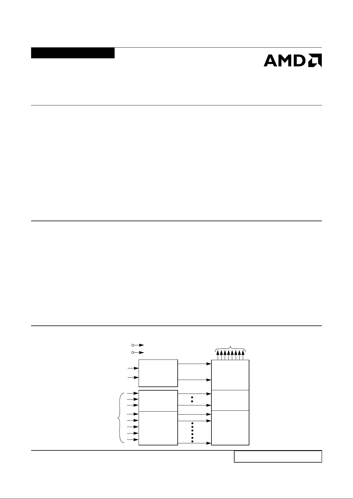
BLOCK DIAGRAM
12079F-1
A0–A15
Address
Inputs
CE#
OE#
V
CC
V
SS
Data Outputs DQ0–DQ15
Output
Buffers
Y
Gating
1,048,576
Bit Cell
Matrix
X
Decoder
Y
Decoder
Output Enable
Chip Enable
and
Prog Logic
2 Am27X1024
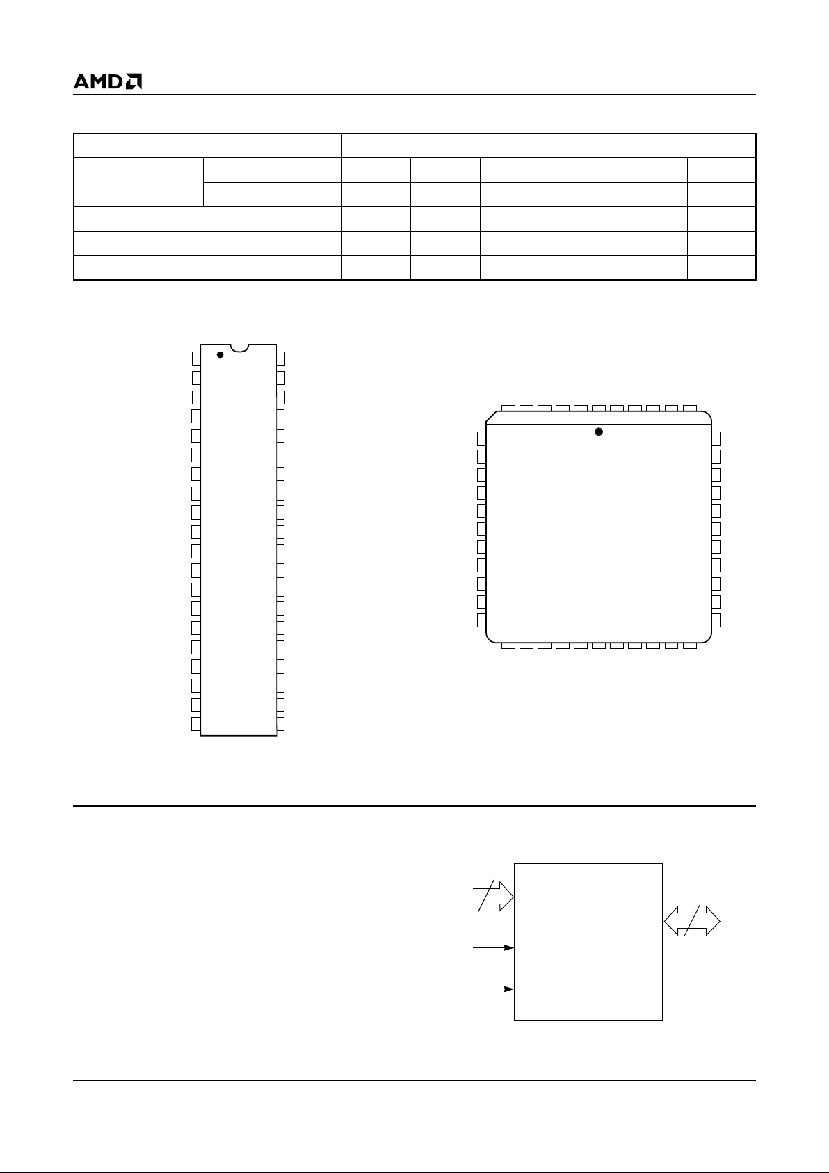
PRODUCT SELECTOR GUIDE
CONNECTION DIAGRAMS
DIP PLCC
Notes:
1. JEDEC nomenclature is in parenthesis.
2. Don’t use (DU) for PLCC.
PIN DESIGNATIONS
A0–A15 = Address Inputs
CE# (E#) = Chip Enable Input
DQ0–DQ15 = Data Input/Outputs
OE# (G#) = Output Enable Input
PGM# (P#) = Program Enable Input
V
CC
=VCC Supply Voltage
V
PP
= Program Voltage Input
V
SS
= Ground
NC = No Internal Connection
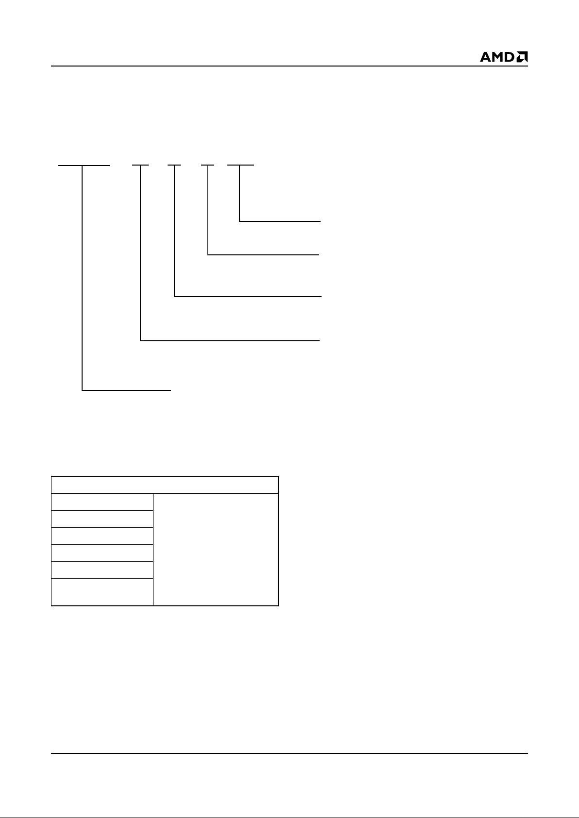
LOGIC SYMBOL
Family Part Number Am27X1024
Speed Options
V
CC
= 5.0 V ± 5% -255
V
CC
= 5.0 V ± 10% -70 -90 -120 -150 -200
Max Access Time (ns) 70 90 120 150 200 250
CE# (E#) Access (ns) 70 90 120 150 200 250
OE# (G#) Access (ns) 70 45 50 65 75 75
1
2
3
4
5
6
7
8
9
10
11
12
13
14
15
16
17
18
19
20
40
39
38
37
36
35
34
33
32
31
30
29
28
27
26
25
24
23
22
21
V
CC
PGM# (P#)
NC
A15
A14
A13
A12
A11
A10
A9
V
SS
A8
A7
A6
A5
A4
A3
A2
A1
A0
V
PP
CE# (E#)
DQ15
DQ14
DQ13
DQ12
DQ11
DQ10
DQ9
DQ8
V
SS
DQ7
DQ6
DQ5
DQ4
DQ3
DQ2
DQ1
DQ0
OE# (G#)
12079F-2
1 444342543264140
7
8
9
10
11
12
13
14
15
16
17
A13
A12
A11
A10
A9
V
SS
NC
A8
A7
A6
A5
DQ13
DQ14
DQ15
CE (E)
VPPDU (Note 2)
VCCPGM# (P#)NCA15
A14
39
38
37
36
35
34
33
32
31
30
29
DQ12
DQ11
DQ10
DQ9
DQ8
V
SS
NC
DQ7
DQ6
DQ5
DQ4
DQ3
DQ2
DQ1
DQ0
OE# (G#)
DU (Note 2)
A0A1A2A3A4
23 24 25 2619 20 21 2218 27 28
12079F-3
16
16
DQ0–DQ15
A0–A15
CE# (E#)
OE# (G#)
12079F-4
Am27X1024 3
ORDERING INFORMATION
Standard Pr od ucts
AMD standard products are available in several packages and operating ranges. The order number (Valid Combination) is formed
by a combination of the following:
Valid Combinations
Valid Combinations list configurations planned to be supported in volume for this device. Consult the local AMD sales
office to confirm availability of specific valid combinations and
to check on newly released combinations.
DEVICE NUMBER/DESCRIPTION
Am27X1024
1 Megabit (64 K x 16-Bit) CMOS ExpressROM Device
AM27X1024
-70 J C
CODE DESIGNATION
Assigned by AMD
TEMPERATURE RANGE
C = Commercial (0°C to +70
°C)
I=Industrial (–40
°C to +85°C)
PACKAGE TYPE
P = 40-Pin Plastic Dual In-Line Package (PD 040)
J = 44-Pin Plastic Leaded Chip Carrier (PL 044)
SPEED OPTION
See Product Selector Guide and Valid Combinations
XXXXX
Valid Combinations
AM27X1024-70
PC, JC, PI, JI
AM27X1024-90
AM27X1024-120
AM27X1024-150
AM27X1024-200
AM27X1024-255
V
CC
= 5.0 V ± 5%
4 Am27X1024
FUNCTIONAL DESCRIPTION
Read Mode
T o obtain dat a at the device outputs, Chip Enable ( CE#)
and Output Enable (OE#) must be driv en low . CE# controls the power to the de vice and is typically used t o select the device . OE# en ables th e de v ice to out put dat a,
independent of device selection. Addresses must be
stable for at least t
ACC–tOE.
Refer to the Switching
Waveforms section for the timing diagr am.
Standby Mode
The device enters the CMOS standby mode when CE#
is at V
CC
± 0.3 V. Maximum V
CC
current is reduced to
100 µA. The device enters the TTL-standby mode
when CE# is at V
IH
. Maximum V
CC
current is reduced
to 1.0 mA. When in either standby mode, the device
places its outputs in a high-impedance state, independent of the OE# input.
Output OR-Tieing
To accommodate multiple memory connections, a
two-line control function provides:
■ Low memory power dissipation, and
■ Assurance that output bus contention will not occur.
CE# should be decoded and used as the primary device-selecting function, while OE# be made a common
connection to all devices in the array and connected to
the READ line from the system control bus. This assures that all deselected memory devices are in their
low-power standby mode and that the output pins are
only active when data is desired from a particular memory device.
System Applications
During the switch between active and standby conditions, transient current peaks are produced on the rising and falling edges of Chip Enab le . The magnitude of
these transient current peaks is dependent on the output capacitance loading of the de vi ce. At a minim um, a
0.1 µF ceramic capacitor (high frequency, low inherent
inductance) sho uld be used on each device between
V
CC
and VSS to minimize transient effects. In addition,
to overcome the voltage drop caused by the inductive
effects of the printed circuit board traces on ExpressROM device arrays, a 4.7 µF bulk electrolytic capacitor
should be used between V
CC
and VSS for each eight
devices. The location of the capacitor should be close
to where the power supply is connected to the array.
MODE SELECT TABLE
Note:
X = Either V
IH
or VIL.
Mode CE# OE# PGM# V
PP
Outputs
Read V
IL
V
IL
XXD
OUT
Output Disable X V
IH
X X High Z
Standby (TTL) V
IH
X X X High Z
Standby (CMOS) V
CC
± 0.3 V X X X High Z

Am27X1024 5
ABSOLUTE MAXIMUM RATINGS
Storage Temperature
OTP Products. . . . . . . . . . . . . . . . . . –65°C to +125°C
Ambient Temperature
with Power Applied. . . . . . . . . . . . . . –55°C to +125°C
Voltage with Respect to V
SS
All pins except VCC . . . . . . . . . –0.6 V to VCC + 0.6 V
V
CC
(Note 1). . . . . . . . . . . . . . . . . . . . .–0.6 V to 7.0 V
Note:
1. Minimum DC voltage on inpu t or I/O pins – 0.5 V. D uring
voltage transitions, the input may overshoot V
SS
to –2.0 V
for periods of up to 20 ns. Max imum DC voltage o n inp ut
and I/O pins is V
CC
+ 5 V . During voltage transitions, input
and I/O pins may overshoot to V
CC
+ 2.0 V for periods up
to 20 ns.
Stresses above those listed under “Abso lute Maximum Ratings” may cause per mane nt dam age to the device. This is a
stress rating only; fun ctio nal ope ration of t he d evice at these
or any other condition s above those indicated in the operational sections of this specification is not implied. Exposure of
the device to absolute maximum ratings for extended periods
may affect device reliability.
OPERATING RANGES
Commercial (C) Devices
Ambient Temperature (T
A
) . . . . . . . . . . .0°C to +70°C
Industrial (I) Devices
Ambient Temperature (T
A
) . . . . . . . . .–40°C to +85°C
Supply Read Voltages
V
CC
for ± 5% devices . . . . . . . . . . +4.75 V to +5.25 V
V
CC
for ± 10% devices . . . . . . . . . +4.50 V to +5.50 V
Operating ranges define those limits between which the functionality of the device is guaranteed.

6 Am27X1024
DC CHARACTERISTICS over operating range (unless otherwise specified)
Caution: The device must not be removed from (or inserted into) a socket when VCC or VPP is applied.
Notes:
1. V
CC
must be applied simultaneously or before VPP, and removed simultaneously or after VPP..
2. I
CC1
is tested with OE# = V
IH
to simulate open outputs.
3. Minimum DC Input Voltage is –0.5 V. During transitions, the inputs may overshoot to –2.0 V for periods less than 20 ns.
Maximum DC Voltage on output pins is V
CC
+ 0.5 V, which may overshoot to VCC + 2.0 V for periods less than 20 ns.
Figure 1. Typical Supply Current vs. Frequency
V
CC
= 5.5 V, T = 25°C
Figure 2. Typical Supply Current vs. Temperature
V
CC
= 5.5 V, f = 10 MHz
Parameter
Symbol Parameter Description Test Conditions Min Max Unit
V
OH
Output HIGH Voltage IOH = –400 µA 2.4 V
V
OL
Output LOW Voltage IOL = 2.1 mA 0.45 V
V
IH
Input HIGH Voltage 2.0 VCC + 0.5 V
V
IL
Input LOW Voltage –0.5 +0.8 V
I
LI
Input Load Current VIN = 0 V to V
CC
1.0 µA
I
LO
Output Leakage Current V
OUT
= 0 V to V
CC
1.0 µA
I
CC1
VCC Active Current (Note 2) CE# = VIL, f = 10 MHz,
I
OUT
= 0 mA
50 mA
I
CC2
VCC TTL Standby Current CE# = V
IH
1.0 mA
I
CC3
VCC CMOS Standby Current CE# = VCC ± 0.3 V 100 µA
12079F-5
12345678910
40
35
30
25
20
Frequency in MHz
Supply Current
in mA
12079F-6
–75 –50 –55 0 25 50 75 100 125 150
40
35
30
25
20
Temperature in °C
Supply Current
in mA
Am27X1024 7
TEST CONDITIONS
Table 1. Test Specifications
SWITCHING TEST WAVEFORM
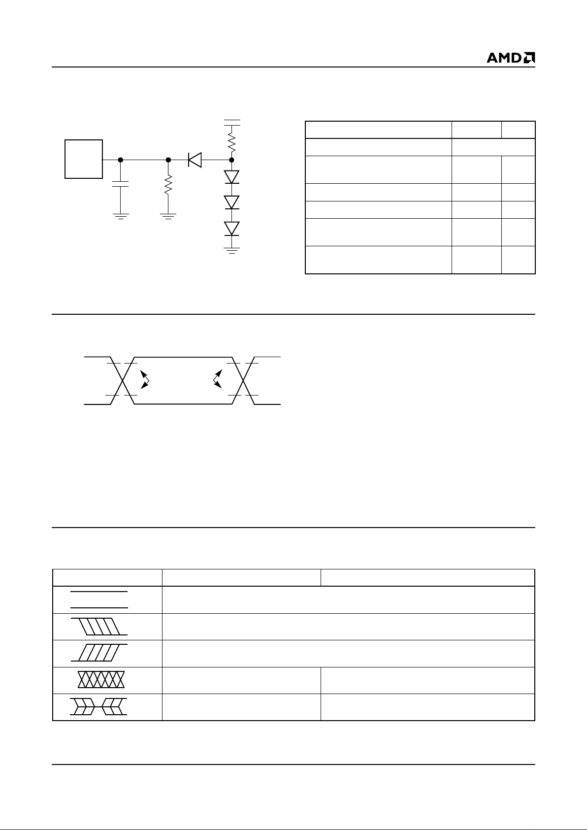
KEY TO SWITCHING WAVEFORMS
2.7 kΩ
C
L
6.2 kΩ
5.0 V
Device
Under
Test
12079F-7
Figure 3. Test Setup
Note:
Diodes are IN3064 or equivalents.
Test Condition All Unit
Output Load 1 TTL gate
Output Load Capacitance, C
L
(including jig capacitance)
100 pF
Input Rise and Fall Times ≤ 20 ns
Input Pulse Levels 0.45–2.4 V
Input timing measurement reference
levels
0.8, 2.0 V
Output timing measurement
reference levels
0.8, 2.0 V
2.4 V
0.45 V
Input
Output
Test Points
2.0 V
2.0 V
0.8 V
0.8 V
12079F-8
Note: For CL = 100 pF.
KS000010-PAL
WAVEFORM INPUTS OUTPUTS
Steady
Changing from H to L
Changing from L to H
Don’t Care, Any Change Permitted Changing, State Unknown
Does Not Apply Center Line is High Impedance State (High Z)
8 Am27X1024
AC CHARACTERISTICS
Caution: Do not remove the device from (or insert it into) a socket or board that has VPP or V
CC
applied.
Notes:
1. VCC must be applied simultaneously or before VPP, and removed simultaneously or after VPP.
2. This parameter is sampled and not 100% tested.
3. Switching characteristics are over operating range, unless otherwise specified.
4. See Figure 3 and Table 1 for test specifications.
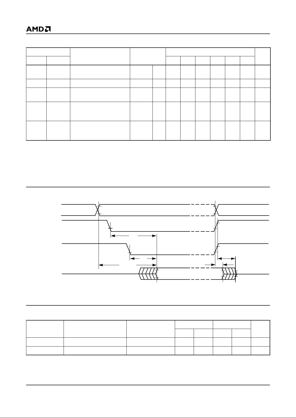
SWITCHING WAVEFORMS
Notes:
1. OE# may be delayed up to t
ACC
– tOE after the falling edge of the addresses without impact on t
ACC
.
2. t
DF
is specified from OE# or CE#, whichever occurs first.
PACKAGE CAPACITANCE
Notes:
1. This parameter is only sampled and not 100% tested.
2. T
A
= +25°C, f = 1 MHz.
Parameter Symbols
Description Test Setup
Am27X1024
UnitJEDEC Standard -70 -90 -120 -150 -200 -255
t
AVQV
t
ACC
Address to Output Delay
CE#,
OE# = V
IL
Max 70 90 120 150 200 250 ns
t
ELQV
t
CE
Chip Enable to Output Delay OE# = VILMax 70 90 120 150 200 250 ns
t
GLQV
t
OE
Output Enable to Output
Delay
CE# = V
IL
Max404550657575ns
t
EHQZ
t
GHQZ
t
DF
(Note 2)
Chip Enable High or Output
Enable High to Output High Z,
Whichever Occurs First
Max304050505050ns
t
AXQX
t
OH
Output Hold Time from
Addresses, CE# or OE#,
Whichever Occurs First
Min000000ns
Addresses
CE#
OE#
Output
12079F-9
Addresses Valid
High Z
High Z
t
CE
Valid Output
2.4
0.45
2.0
0.8
2.0
0.8
t
ACC
(Note 1)
t
OE
tDF (Note 2)
t
OH
Parameter
Symbol Parameter Description Test Conditions
PD 040 PL 044
UnitTyp Max Typ Max
C
IN
Input Capacitance VIN = 0 7 12 8 10 pF
C
OUT
Output Capacitance V
OUT
= 0 11 14 11 14 pF

Am27X1024 9
PHYSICAL DIMENSIONS
PD 040—40-Pin Plastic Dual In-Line Package (measured in inches)
PL 044—44-Pin Plastic Leaded Chip Carrier (measured in inches)
Pin 1 I.D.
2.040
2.080
.530
.580
.005 MIN
.045
.065
.090
.110
.140
.225
.120
.160
.014
.022
SEATING PLANE
.015
.060
16-038-SC_AF
PD 040
DG76
2-28-95 ae
40
21
20
.630
.700
0°
10°
.600
.625
.008
.015
TOP VIEW
SEATING PLANE
.685
.695
.650
.656
Pin 1 I.D.
.685
.695
.650
.656
.026
.032
.050 REF
.042
.056
.062
.083
.013
.021
.590
.630
.500
REF
.009
.015
.165
.180
.090
.120
16-038-SQ
PL 044
EC80
11.3.97 lv
SIDE VIEW

10 Am27X1024
REVISION SUMMARY FOR AM27X1024
Revision F
Global
Changed formatting to match current data sheets.
Trademarks
Copyright © 1998 Advanced Micro D evices, Inc. All r ights reserved.
AMD, the AMD logo, and combinations thereof are trademarks of Advanced Micro Devices, Inc.
Flashrite is a trademark of Advanced Micro Devices, Inc.
Product names used in this publication are for identification purposes only and may be trademarks of their respective companies.
 Loading...