

查询S3062供应商
3
S3067MULTIRATE (OC-48/24/12/3/GBE/FC) SONET/SDH/ATM TRANSCEIVER w/ FEC
September 17, 2002/ Revision A
S3067 OVERVIEW
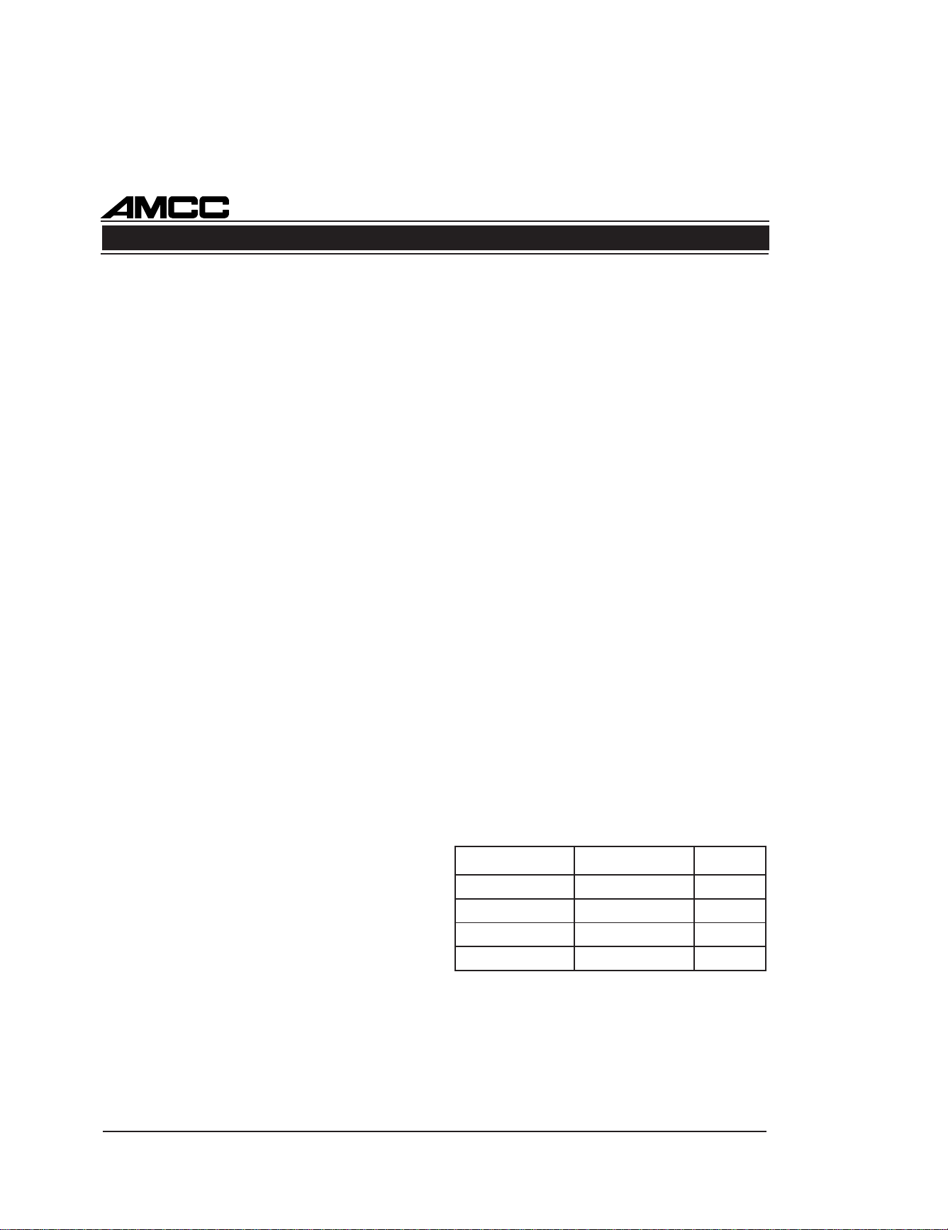
The S3067 transceiver implements SONET/SDH
and WDM serialization/deserialization, and transmission functions. The block diagram in Figure 4 shows
the basic operation of the chip. This chip can be
used to implement the front end of WDM equipment,
which consists primarily of the serial transmit interface and the serial receive interface. The chip
handles all the functions of these two elements, including parallel-to-serial and serial-to-parallel
conversion, clock generation, and system timing.
The system timing circuitry consists of management
of the data stream and clock distribution throughout
the front end.
S3067 has the ability to bypass the internal VCO
with an external source and also with the receive
clock. The device generates 14/15, 15/14, 16/17 and
17/16 clocks based upon the received clock and an
external clock to incorporate the FEC capability. The
dividers support the first two rates shown in Table 4.
The S3067 is divided into a transmitter section and a
receiver section. The sequence of operations is as
follows:
0LESETAR1LESETARedoMgnitarepO
00 3-CO
01 21-CO
10 CF/EBG/42-CO
11 84-CO
Table 2. Data Rate Select
Transmitter Operations:
1. 16-bit parallel input
2. Parallel-to-serial conversion
3. Serial output
Receiver Operations:
1. Serial input
2. Serial-to-parallel conversion
3. 16-bit parallel output
Internal clocking and control functions are transparent to the user. S3067 Supports six different code
rates, besides the normal rate, for each of the four
operating modes.
ytilibapaCgnitcerroCrorrE
gniwohsetaRedoC
eudnoisnapxEhtdiwdnaB
BSF&sdrowedocot
kcolctupnidesaercnifoelpmaxE
)zHM(61-MTS/84-STSrofycneuqerf
kcolbetyb-552repsetyb8esaercni%41.7=832/552 36.661=41/51*25.551=832/552*25.551
kcolbetyb-552repsetyb7esaercni%52.6=042/552 42.561=61/71*25.551=042/552*25.551
kcolbetyb-552repsetyb6esaercni%73.5=242/55278.361=242/552*25.551
kcolbetyb-552repsetyb5esaercni%15.4=442/55235.261=442/552*25.551
kcolbetyb-552repsetyb4esaercni%66.3=642/552 12.161=28/58*25.551=642/552*25.551
kcolbetyb-552repsetyb3esaercni%28.2=842/55219.951=842/552*25.551
Table 4. FEC Modes
Table 3. FEC Select
0CEF12
OCV
rediviD
KLCSR
rediviD
001 7161
101 6171
011 5141
111 4151
000 71X
100 61X
010 51X
110 41X
CCMA6703SeciveDyrevoceRkcolC84-CO
CCMA2603SrotinoMecnamrofreP84-CO
Suggested Interface Devices
4
S3067
MULTIRATE (OC-48/24/12/3/GBE/FC) SONET/SDH/ATM TRANSCEIVER w/ FEC
September 17, 2002/ Revision A
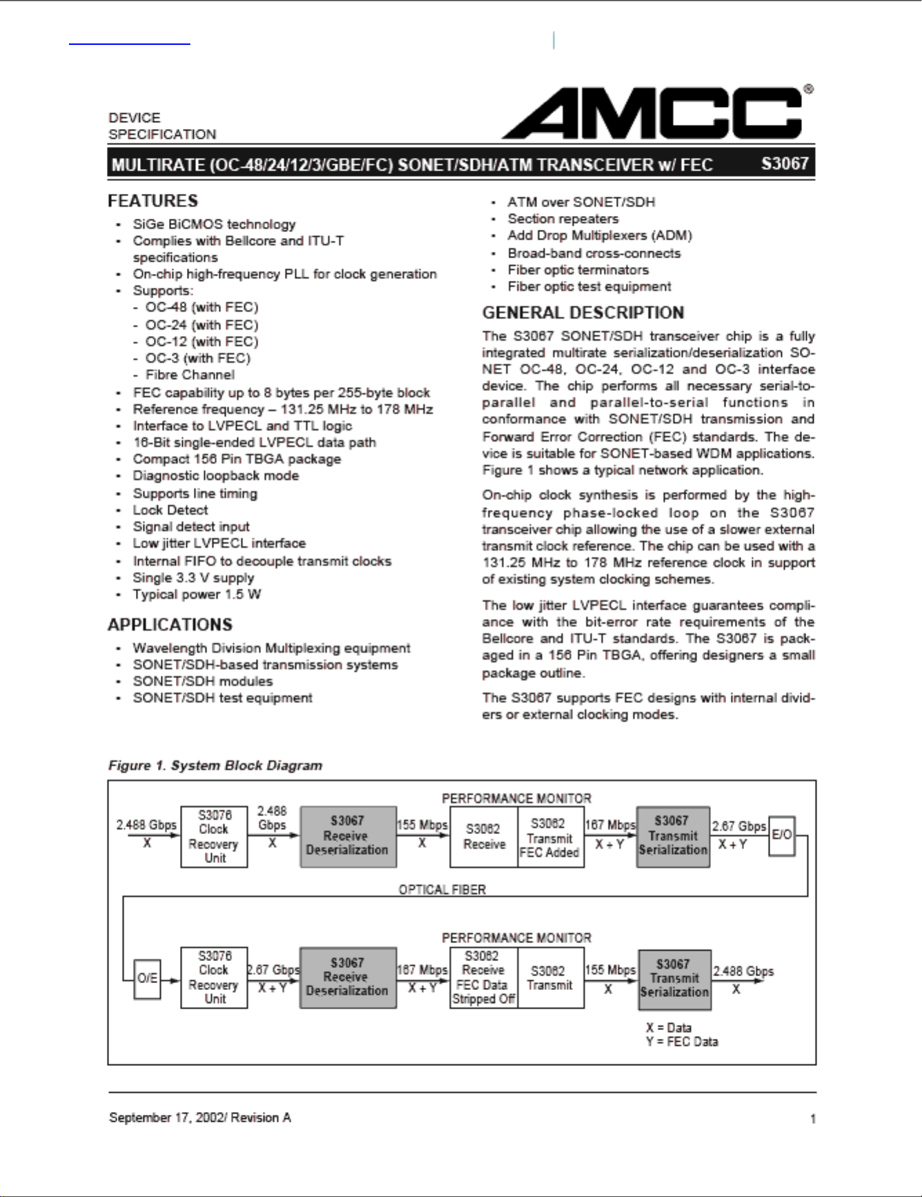
Figure 4. S3067 Transceiver Functional Block Diagram
CLOCKS
LOCKDET
155MCKP/N
19MCK
PCLKP/N
PHERR
TSDP/N
TSCLKP/N
OVREF
POUT[15:0]
POCLKP/N
TIMGEN
16:1
PARALLEL
TO SERIAL
CLOCK
SYNTHESIZER
D
TXDP/N
TXCLKP/N
POCLK (Internal)
REFCLKP/N
PICLKP/N
TXDP/N
(Internal)
TXCLKP/N
(Internal)
RSCLKP/N
DLEB
SQUELCH
IVREF
RSTB
SDLVPECL
SDTTL
RSDP/N
KILLRXCLK
LLEB
PIN[15:0]
BYPASS
TESTEN
CAP2
CAP1
RLPTIME
FECSEL2
PHINIT
D
D
D
1:16
SERIAL TO
PARALLEL
TIMGEN
R
3
16
16
RATESEL[0:1]
FECSEL[2:0]
BYPASSCLKP/N
N
SLPTIME
VCO CLOCK
TX
RX
2

5
S3067MULTIRATE (OC-48/24/12/3/GBE/FC) SONET/SDH/ATM TRANSCEIVER w/ FEC
September 17, 2002/ Revision A
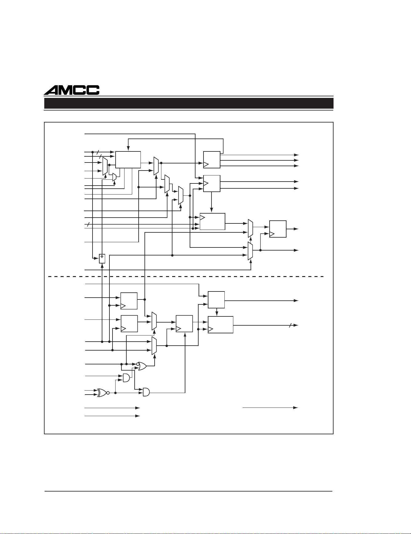
Figure 5. Clock Synthesizer
M
N
PD
LPF
VCO
VCOCLK
REFCLK
FECSEL (0-1)
FECSEL 2
RSCLK
Where N = 14/15/16/17
M = 14/15/16/17
RSCLK N
VCOCLK M
RSCLK Divider
VCO Divider
=
A high on FECSEL2 selects RSCLK divided by N. A
low on FECSEL2 selects the REFCLK. The REFCLK
or RSCLK divided by N is divided by 1/M (multiplied
by M) in the loop. The value of M and N can be
selected by FECSEL0 and FECSEL1.
When FECSEL2 = 0, VCOCLK = REFCLK * M. The
user must select the proper value of REFCLK and M
to get the desired VCOCLK frequency. When
FECSEL2 = 1, VCOCLK = (RSCLK * M) ÷ N. The
user must select the proper M/N ratio (with
FECSEL0 and FECSEL1) to get the desired
VCOCLK value. (See Tables 3 and 4.)
Example: OC-48 FEC capability of 8 bytes per
255-byte block. Required VCOCLK = 2.6656 GHz.
Method 1:
Required VCOCLK = 2.6656 GHz
FECSEL2 = 0, selects REFCLK
FECSEL0 = 1 and FECSEL1 = 0, selects VCO
divider(M) = 16
REFCLK = 2.6656 GHz ÷ 16 = 166.60 MHz
VCOCLK = REFCLK ÷ (1/M) = 166.60 * 16 = 2.6656
GHz
Method 2:
Required VCOCLK = 2.6656 GHz
FECSEL2 = 1, selects RSCLK
FECSEL0 = 0 and FECSEL1 = 0, selects VCO
divider(M) = 17 and RSCLK divider(N) = 16
RSCLK = (2.6656 * 16) ÷ 17 = 2.5088 GHz
VCOCLK = RSCLK ÷ N ÷ (1/M) = 2.5088 GHz ÷ 16 *
17 = 2.6656 GHz.
6
S3067
MULTIRATE (OC-48/24/12/3/GBE/FC) SONET/SDH/ATM TRANSCEIVER w/ FEC
September 17, 2002/ Revision A
S3067 TRANSCEIVER
FUNCTIONAL DESCRIPTION
Transmitter Operation
The S3067 transceiver chip performs the serialization
stage in the processing of a transmit SONET STS-48/
STS-24/STS-12/STS-3/GBE/FC data stream depending on the data rate selected. It converts 16-bit
parallel data to bit serial format.
A high-frequency bit clock can be generated from a
131.25 MHz to 178 MHz frequency reference by using an integral frequency synthesizer consisting of a
phase-locked loop circuit with a divider in the loop.
Diagnostic loopback (transmitter to receiver) and line
loopback (receiver to transmitter) is provided. See
Other Operating Modes
.
The bypass signal selects between the BYPASSCLK
and the VCO clock. BYPASSCLK can be used to provide an alternative clock to the internal VCO when the
user selects an error correcting capability which is not
provided by the S3067 dividers. The user must provide the required frequency for the BYPASSCLK
when error-correcting capability of 6/5/4/3 bytes per
255-byte block is selected.
Clock Synthesizer
The clock synthesizer, shown in the block diagrams
of Figures 4 and 5, is a monolithic PLL that generates the serial output clock frequency locked to the
input Reference Clock (REFCLKP/N).
The REFCLKP/N input must be generated from a
crystal oscillator that has a frequency accuracy better than the value stated in Table 10 in order for the
TSCLK frequency to have the accuracy required for
operation in a SONET system. Lower-accuracy crystal oscillators may be used in applications less
demanding than SONET/SDH.
The on-chip PLL consists of a phase detector, which
compares the phase relationship between the VCO
output and the REFCLKP/N input, a loop filter which
converts the phase detector output into a smooth DC
voltage, and a VCO, whose frequency is varied by
this voltage.
The divide by ‘N’ and divide by ‘M’ provide the
counters required to support error correcting capability. The values of ‘N’ and ‘M’ can be selected by
FECSEL lines.
The loop filter generates a VCO control voltage
based on the average DC level of the phase discriminator output pulses. A single external clean-up
capacitor is utilized as part of the loop filter. The loop
filter’s corner frequency is optimized to minimize output phase jitter.
Timing Generator
The timing generation function, seen in Figure 4,
provides a divide-by-16 version of the transmit serial
clock. This circuitry also provides an internally generated load signal, which transfers the PIN[15:0]
data from the parallel input register to the serial shift
register.
The PCLK output is a divide-by-16 rate version of
transmit serial clock (divide-by-16). PCLK is intended for use as a divide-by-16 clock for upstream
multiplexing and overhead processing circuits. Using
PCLK for upstream circuits will ensure a stable frequency and phase relationship between the data
coming into and leaving the S3067 device.
The timing generator also produces a feedback reference clock to the clock synthesizer. A counter
divides the synthesized clock down to the same frequency as the reference clock REFCLK. The PLL in
the clock synthesizer maintains the stability of the
synthesized clock by comparing the phase of the
internal clock with that of the Reference Clock
(REFCLK).
Table 5. Reference Jitter Limits
edoMgnitarepOhtdiWdnaBrettiJSMR
84-STSzHM02otzHk21cBd1642-STSzHM01otzHk21sp2
21-STSzHM5otzHk21sp4
3-STSzHM1otzHk21sp61

7
S3067MULTIRATE (OC-48/24/12/3/GBE/FC) SONET/SDH/ATM TRANSCEIVER w/ FEC
September 17, 2002/ Revision A
Parallel-to-Serial Converter
The parallel-to-serial converter shown in Figure 4 is
comprised of a FIFO and a parallel-to-serial register.
The FIFO input latches the data from the PIN[15:0]
bus on the rising edge of PICLK. The parallel-toserial register is a loadable shift register which takes
its parallel input from the FIFO output.
An internally generated divide-by-16 clock, which is
phase aligned to the transmit serial clock as described in the
Timing Generator
description, activates
the parallel data transfer between registers. The serial
data is shifted out of the parallel-to-serial register at
the TSCLK rate
.
FIFO
A FIFO is added to decouple the internal and external (PICLK) clocks. The internally generated
divide-by-16 clock is used to clock out data from the
FIFO. PHINIT and LOCKDET are used to center or
reset the FIFO. The PHINIT and LOCKDET signals
will center the FIFO after the third PICLK pulse. This
is to insure that PICLK is stable. This scheme allows
the user to have an infinite PCLK-to-PICLK delay
through the ASIC. Once the FIFO is centered, the
PCLK-to-PICLK delay can have a maximum drift as
specified in Table 20.
FIFO Initialization
The FIFO can be initialized in one of the following
three ways:
1. During power up, once the PLL has locked to
the reference clock provided on the REFCLK
pins, the LOCKDET will go active and initialize
the FIFO.
2. When RSTB goes active, the entire chip is reset.
This causes the PLL to go out of lock and thus
the LOCKDET goes inactive. When the PLL reacquires the lock, the LOCKDET goes active
and initializes the FIFO. Note: PCLK is held reset when RSTB is active.
3. The user can also initialize the FIFO by raising
PHINIT.
During the normal running operation, the incoming
data is passed from the PICLK timing domain to the
internally generated, divide-by-16 clock timing domain. Although the frequency of PICLK and the
internally generated clock is the same, their phase
relationship is arbitrary. To prevent errors caused by
short setup or hold times between the two timing
domains, the timing generator circuitry monitors the
phase relationship between PICLK and the internally
generated clock. When a potential setup or hold time
violation is detected, the phase error goes high.
When PHERR conditions occur, PHINIT should be
activated to recenter the FIFO (at least 2 PCLK periods). This can be done by connecting PHERR to
PHINIT. When realignment occurs, up to 10 bytes of
data will be lost. The user can also take in the
PHERR signal, process it and send an output to
PHINIT in such a way that idle bytes are lost during
the realignment process. PHERR will go inactive
when the realignment is complete.
Receiver Operation
The S3067 receiver chip provides the first stage of
digital processing of a receive SONET STS-48/STS24/STS-12/STS-3/GBE/FC bit-serial stream. The
bit-serial data stream is then converted into a 16-bit
half-word data format. A loopback mode is provided
for diagnostic loopback (transmitter to receiver). A line
loopback (receiver to transmitter) is also provided.
Both line and local loopback modes can be active at
the same time.
Serial-to-Parallel Converter
The serial-to-parallel converter consists of two 16-bit
registers. The first is a serial-in, parallel-out shift register, which performs the serial-to-parallel conversion
clocked by the clock recovery block. On the falling
edge of the POCLK, the data in the parallel register
is transferred to an output parallel register which
drives POUT[15:0].
OTHER OPERATING MODES
Diagnostic Loopback
When the Diagnostic Loopback Enable (DLEB) input
is low, a loopback from the transmitter to the receiver at the serial data rate can be set up for
diagnostic purposes. The differential serial output
data from the transmitter is routed to the serial-toparallel block in place of the normal data stream
(RSD). TSD/TSCLK outputs are active. DLEB takes
precedence over SDPECL and SDTTL.

8
S3067
MULTIRATE (OC-48/24/12/3/GBE/FC) SONET/SDH/ATM TRANSCEIVER w/ FEC
September 17, 2002/ Revision A
Line Loopback
The line loopback circuitry selects the source of the
data and clock which is output on TSD and TSCLK.
When the Line Loopback Enable input (LLEB) is
high, it selects data and clock from the parallel-toserial converter block. When LLEB is low, it forces
the output data multiplexer to select the data and
clock from the RSD and RSCLK inputs, and a receive-to-transmit loopback can be established at the
serial data rate. Diagnostic loopback and line
loopback can be active at the same time.
Loop Timing
In Serial Loop Timing mode (SLPTIME), the clock
synthesizer PLL of the S3067 is bypassed, and the
timing of the entire transmitter section is controlled
by the Receive Serial Clock, RSCLKP/N. This mode
is entered by setting the SLPTIME input to a TTL
high level.
In this mode, the REFCLKP/N input is not used, and
the RATESEL input is ignored for all transmit functions. It should be carefully noted that the internal
PLL continues to operate in this mode and continues
as the source for the 19MCK and 155MCK. Therefore these signals are being used (e.g. as the
reference for an external S3076 clock recovery device), the REFCLKP/N and RATESEL inputs must
be properly driven.
In Reference Loop Timing mode (RLPTIME), the
Parallel Clock from the receiver (POCLK) is used as
the reference clock to the transmitter. In this mode,
the REFCLKP/N input is not used. The 19MCK and
155MCK are generated from the POCLK in this operating mode. When operating the S3067 in
RLPTIME mode, the 19MCK and 155MCK outputs
should not be used as the back-up reference clock
for a clock and data recovery device (S3066,
S3040). When performing loopback testing (DLEB),
the S3067 must not be in RLPTIME.
Squelched Clock
Operation
Some integrated optical receiver/clock recovery
modules force their recovered serial receive clock
output to the logic zero state if the optical signal is
removed or reduced below a fixed threshold. This
condition is accompanied by the expected
deassertion of the Signal Detect (SD) output.
The S3067 has been designed for operation with
clock recovery devices that provide continuous serial
clock for seamless downstream clocking in the event
of optical signal loss.
For operation with an optical transceiver that provides the
Squelched Clock
behavior as described
above, the S3067 can be operated in the
Squelched
Clock
mode by activating the SQUELCH pin.
In this condition, the Receive Serial Clock (RSCLKP/N)
is used for all receiver timing when the SDLVPECL/
SDTTL inputs are in the active state. When the
SDLVPECL/SDTTL inputs are placed in the inactive
state (usually by the deassertion of LOCKDET or Signal Detect from the optical transceiver/clock recovery
unit), the transmitter serial clock will be used to maintain timing in the receiver section. This will allow the
POCLK to continue to run and the parallel outputs to
flush out the last received characters and then assume
the all-zero state imposed at the serial data input.
It is important to note that in this mode there will be
a one-time shortening or lengthening of the POCLK
cycle, resulting in an apparent phase shift in the
POCLK at the deassertion of the SD condition. Another similar phase shift will occur when the SD
condition is reasserted.
In the normal operating mode, with SQUELCH inactive, there will be no phase discontinuities at the
POCLK output during signal loss or reacquisition
(assuming operation with continuous clocking from
the CRU device such as the AMCC S3076).

9
S3067MULTIRATE (OC-48/24/12/3/GBE/FC) SONET/SDH/ATM TRANSCEIVER w/ FEC
September 17, 2002/ Revision A
Table 6. S3067 Transmitter Pin Assignment and Descriptions
emaNniPleveLO/I#niPnoitpircseD
0NIP
1NIP
2NIP
3NIP
4NIP
5NIP
6NIP
7NIP
8NIP
9NIP
01NIP
11NIP
21NIP
31NIP
41NIP
51NIP
elgniS
dednE
LCEPVL
I2A
3B
2B
3C
1A
2C
1B
2D
3E
1C
2E
3F
2F
1E
1F
3G
lellarap,KLCIPehtotdengila,61-yb-edividA.tupnIataDlellaraP
otgnidnopserroc(tibtnacifingistsomehtsi]51[NIP.kcolctupni
ehtsi]0[NIP.)dettimsnarttibtsrifeht,drowMCPhcaefo1tib
,drowMCPhcaefo61tibotgnidnopserroc(tibtnacifingistsael
egdegnisirehtnodelpmassi]0:51[NIP.)dettimsnarttibtsaleht
.KLCIPfo
PKLCIP
NKLCIP
yllanretnI
desaiB
.ffiD
LCEPVL
I4A
3A
elcycytud%05yllanimon,61-yb-edividA.kcolCtupnIlellaraP
otdesusiKLCIP.dengilasi]0:51[NIPhcihwot,kcolctupni
ehtniretsigergnidlohaotnistupniNIPehtnoatadehtrefsnart
selpmasKLCIPfoegdegnisirehT.retrevnoclaires-ot-lellarap
.]0:51[NIP
1PAC
2PAC
golanAI5R
5T
dnaroticapacretlifpoollanretxeehT.roticapaCretliFpooL
.62erugiFeeS.snipesehtotdetcennocerasrotsiser
FERVICDI 4C.egatlovecnerefertupniLCEPVLdedne-elgniS
TINIHPelgniS
dednE
LCEPVL
I2G.gnimitlanretningilaerlliwegdegnisiR.noitazilaitinIesahP
PDST
NDST
.ffiD
LMC
O11R
21R
,slangismaertsatadlairesLMClaitnereffiD.ataDlaireStimsnarT
.eludomrettimsnartlacitponaotdetcennocyllamron
PKLCST
NKLCST
.ffiD
LMC
O8R
9R
desuebnacN/PKLCSTLMClaitnereffiD.kcolClaireStimsnarT
detceleseblliwycneuqerfkcolcsihT.langisDSTehtemiterot
.LESCEFdnaLESETARyb
PKLCP
NKLCP
.ffiD
LCEPVL
O6C
6B
ybkcolctiblanretniehtgnidividybdetarenegkcolcecnereferA
neewtebsrefsnartediw-drowetanidroocotdesuyllamronsitI.61
.ecived7603Sehtdnacigolmaertspu
RREHPelgniS
dednE
LCEPVL
O5AerehthcihwrofelcycKLCPhcaegnirudhgiHsesluP.rorrEesahP
lanretniehtneewtebnoitaloivgnimitdloh/pu-teslaitnetopasi
ehtnodetadpusiRREHP.sniamodgnimitKLCIPdnakcolcetyb
.stuptuoKLCPehtfoegdegnillaf
 Loading...