

AMCC NPe405L DATA SHEET

查询IBM25NPE405L-3FA133C供应商
AMCC NPe405L
PowerNP
Data Sheet
PowerNP NPe405L Data Sheet
Document Issue 1.00
September 2004
C
OVER

AMCC reserves the right to make changes to its products, its datasheets, or related
documentation, without notice and warrants its products solely pursuant to its
terms and conditions of sale, only to substantially comply with the latest available
datasheet. Please consult AMCC’s Term and Conditions of Sale for its warranties
and other terms, conditions and limitations. AMCC may discontinue any
semiconductor product or service without notice, and advises its customers to
obtain the latest version of relevant information to verify, before placing orders,
that the information is current. AMCC does not assume any liability arising out of
the application or use of any product or circuit described herein, neither does it
convey any license under its patent rights nor the rights of others. AMCC reserves
the right to ship devices of higher grade in place of those of lower grade.
AMCC SEMICONDUCTOR PRODUCTS ARE NOT DESIGNED, INTENDED,
AUTHORIZED, OR WARRANTED TO BE SUITABLE FOR USE IN LIFESUPPOR T APPLICATIONS, DEVICES OR SYSTEMS OR OTHER CRITICAL
APPLICATIONS.
AMCC is a registered Trademark of Applied Micro Circuits Corporation.
Copyright © 2004 Applied Micro Circuits Corporation.

Preliminary
PowerNP NPe405L Embedded Processor Data Sheet
Features
•PowerNP technology using an IBM PowerPC
405 32-bit RISC processor core operating up to
266 MHz
• PC-133 synchronous DRAM (SDRAM) interf ace
- 32-bit interface for non-ECC applications
- 40-bit interface serves 32 bits of data plus 8
check bits for ECC applications
• External bus for peripheral devices
- Flash and ROM interface
- Direct support for 8-, or 16-bit SRAM and
external peripherals
- Up to 4 devices
• DMA support for external peripherals, internal
UARTs and memory
- Scatter-gather chaining supported
- Four channels
• Two 10/100 Ethernet MACs supporting up to
two external PHYs via MII, RMII, or SMII
interfaces
• HDLC interface with 32 channels through two
ports at up to 4.096 Mbps each or 8.192 Mbps
for a single port
• Programmable interrupt controller
- Seven external and 29 internal
- Edge triggered or level-sensitive
- Positive or negative active
- Non-critical or critical interrupt to processor
core
- Programmable critical interrupt priority
ordering
- Programmable critical interrupt vector
• Programmable timers
• Two serial ports (16550 compatible UART)
• One IIC interface
• General Purpose I/O (GPIO) available
• Supports JTAG for board level testing
• Internal processor local bus (PLB) runs at
SDRAM interface frequency
Description
Designed specifically to address embedded
applications, the NPe405L provides a highperformance, low-power solution that interfaces to a
wide range of peripherals by incorporating on-chip
power management features and lower power
dissipation requirements.
This chip contains a high-perfo rmanc e RISC
processor core, SDRAM controller, Ethernet
EMACs, HDLC controller, external bus controller for
While the information contained herein is believed to be accurate, such information is preliminary, and should not be
relied upon for accuracy or completeness, and no representations or warranties of accuracy or completeness are made.
ROM, Flash, and peripherals, DMA with scattergather support, serial ports, IIC interface, and
general purpose I/O.
Technology: IBM CMOS SA-12E 0.25
µm L
(0.18
Package: 23mm, 324-ball enhanced plastic ball grid
array (E-PBGA)
Power (typical): 1.3W at 133MHz, 1.7W at
200MHz, 1.8W at 266MHz
eff
)
µm
1

Preliminary
PowerNP NPe405L Embedded Processor Data Sheet
Contents
Ordering, PVR, and JTAG Information . . . . . . . . . . . . . . . . . . . . . . . . . . . . . . . . . . . . . . . . . . . . . . . . . . . . . . 4
Address Map Support . . . . . . . . . . . . . . . . . . . . . . . . . . . . . . . . . . . . . . . . . . . . . . . . . . . . . . . . . . . . . . . . . . . 5
SDRAM Memory Controller . . . . . . . . . . . . . . . . . . . . . . . . . . . . . . . . . . . . . . . . . . . . . . . . . . . . . . . . . . . . . . 8
External Bus Controller (EBC) . . . . . . . . . . . . . . . . . . . . . . . . . . . . . . . . . . . . . . . . . . . . . . . . . . . . . . . . . . . . 8
DMA Controller . . . . . . . . . . . . . . . . . . . . . . . . . . . . . . . . . . . . . . . . . . . . . . . . . . . . . . . . . . . . . . . . . . . . . . . . 9
Serial Interface . . . . . . . . . . . . . . . . . . . . . . . . . . . . . . . . . . . . . . . . . . . . . . . . . . . . . . . . . . . . . . . . . . . . . . . . 9
IIC Bus Interface . . . . . . . . . . . . . . . . . . . . . . . . . . . . . . . . . . . . . . . . . . . . . . . . . . . . . . . . . . . . . . . . . . . . . . 10
HDLCEX Interface . . . . . . . . . . . . . . . . . . . . . . . . . . . . . . . . . . . . . . . . . . . . . . . . . . . . . . . . . . . . . . . . . . . . 10
General Purpose IO (GPIO) Controller . . . . . . . . . . . . . . . . . . . . . . . . . . . . . . . . . . . . . . . . . . . . . . . . . . . . . 10
Universal Interrupt Controller (UIC) . . . . . . . . . . . . . . . . . . . . . . . . . . . . . . . . . . . . . . . . . . . . . . . . . . . . . . . 10
10/100 Mbps Ethernet MAC . . . . . . . . . . . . . . . . . . . . . . . . . . . . . . . . . . . . . . . . . . . . . . . . . . . . . . . . . . . . . 11
JTAG . . . . . . . . . . . . . . . . . . . . . . . . . . . . . . . . . . . . . . . . . . . . . . . . . . . . . . . . . . . . . . . . . . . . . . . . . . . . . . . 11
Signal Lists . . . . . . . . . . . . . . . . . . . . . . . . . . . . . . . . . . . . . . . . . . . . . . . . . . . . . . . . . . . . . . . . . . . . . . . . . . 13
Signal Description . . . . . . . . . . . . . . . . . . . . . . . . . . . . . . . . . . . . . . . . . . . . . . . . . . . . . . . . . . . . . . . . . . . . . 30
Test Conditions . . . . . . . . . . . . . . . . . . . . . . . . . . . . . . . . . . . . . . . . . . . . . . . . . . . . . . . . . . . . . . . . . . . . . . . 41
Spread Spectrum Clocking . . . . . . . . . . . . . . . . . . . . . . . . . . . . . . . . . . . . . . . . . . . . . . . . . . . . . . . . . . . . . . 43
Initialization . . . . . . . . . . . . . . . . . . . . . . . . . . . . . . . . . . . . . . . . . . . . . . . . . . . . . . . . . . . . . . . . . . . . . . . . . . 51
2

Preliminary
PowerNP NPe405L Embedded Processor Data Sheet
Tables
System Address Map . . . . . . . . . . . . . . . . . . . . . . . . . . . . . . . . . . . . . . . . . . . . . . . . . . . . . . . . . . . . . . . . . . . 6
DCR Address Map . . . . . . . . . . . . . . . . . . . . . . . . . . . . . . . . . . . . . . . . . . . . . . . . . . . . . . . . . . . . . . . . . . . . . 7
Signals Listed Alphabetically . . . . . . . . . . . . . . . . . . . . . . . . . . . . . . . . . . . . . . . . . . . . . . . . . . . . . . . . . . . . 13
Signals Listed by Ball Assignment . . . . . . . . . . . . . . . . . . . . . . . . . . . . . . . . . . . . . . . . . . . . . . . . . . . . . . . . 24
Pin Summary . . . . . . . . . . . . . . . . . . . . . . . . . . . . . . . . . . . . . . . . . . . . . . . . . . . . . . . . . . . . . . . . . . . . . . . . 30
Signal Functional Description . . . . . . . . . . . . . . . . . . . . . . . . . . . . . . . . . . . . . . . . . . . . . . . . . . . . . . . . . . . . 32
Absolute Maximum Ratings . . . . . . . . . . . . . . . . . . . . . . . . . . . . . . . . . . . . . . . . . . . . . . . . . . . . . . . . . . . . . 38
Package Thermal Specifications . . . . . . . . . . . . . . . . . . . . . . . . . . . . . . . . . . . . . . . . . . . . . . . . . . . . . . . . . 38
Recommended DC Operating Conditions . . . . . . . . . . . . . . . . . . . . . . . . . . . . . . . . . . . . . . . . . . . . . . . . . . 39
Input Capacitance . . . . . . . . . . . . . . . . . . . . . . . . . . . . . . . . . . . . . . . . . . . . . . . . . . . . . . . . . . . . . . . . . . . . . 40
DC Electrical Characteristics . . . . . . . . . . . . . . . . . . . . . . . . . . . . . . . . . . . . . . . . . . . . . . . . . . . . . . . . . . . . 41
Clocking Specifications . . . . . . . . . . . . . . . . . . . . . . . . . . . . . . . . . . . . . . . . . . . . . . . . . . . . . . . . . . . . . . . . . 42
Peripheral Interface Clock Timings . . . . . . . . . . . . . . . . . . . . . . . . . . . . . . . . . . . . . . . . . . . . . . . . . . . . . . . . 44
I/O Specifications—All . . . . . . . . . . . . . . . . . . . . . . . . . . . . . . . . . . . . . . . . . . . . . . . . . . . . . . . . . . . . . . . . . 46
I/O Specifications—133 and 200MHz . . . . . . . . . . . . . . . . . . . . . . . . . . . . . . . . . . . . . . . . . . . . . . . . . . . . . 47
I/O Specifications—266MHz . . . . . . . . . . . . . . . . . . . . . . . . . . . . . . . . . . . . . . . . . . . . . . . . . . . . . . . . . . . . 49
Figures
NPe405L Embedded Controller Functional Block Diagram . . . . . . . . . . . . . . . . . . . . . . . . . . . . . . . . . . . . . . 5
23mm, 324-Ball E-PBGA Package . . . . . . . . . . . . . . . . . . . . . . . . . . . . . . . . . . . . . . . . . . . . . . . . . . . . . . . . 12
Input Setup and Hold Waveform . . . . . . . . . . . . . . . . . . . . . . . . . . . . . . . . . . . . . . . . . . . . . . . . . . . . . . . . . 45
Output Delay and Float Timing Waveform . . . . . . . . . . . . . . . . . . . . . . . . . . . . . . . . . . . . . . . . . . . . . . . . . . 45
3

Preliminary
PowerNP NPe405L Embedded Processor Data Sheet
Ordering, PVR, and JTAG Information
Product Name
NPe405L IBM25NPe405L-3FA133C 133M H z 23mm, 324 E-PBGA A 0x416100C0 0x04247409
NPe405L IBM25NPe405L-3FA133CZ 133M H z 23mm, 324 E-PBGA A 0x416100C0 0x04247409
NPe405L IBM25NPe405L-3FA200C 200M H z 23mm, 324 E-PBGA A 0x416100C0 0x04247409
NPe405L IBM25NPe405L-3FA200CZ 200M H z 23mm, 324 E-PBGA A 0x416100C0 0x04247409
NPe405L IBM25NPe405L-3FA266C 266M H z 23mm, 324 E-PBGA A 0x416100C0 0x04247409
NPe405L IBM25NPe405L-3FA266CZ 266M H z 23mm, 324 E-PBGA A 0x416100C0 0x04247409
Note 1: Z at the end of the Order Part Number indicates a tape and reel shipping package. Otherwise, the chips are shipped in a tray.
Order Part Number
1
Processor
Frequency
Package
Rev
Level
PVR Value JTAG ID
This section provides the part numbering nomenclature for the NPe405L. For availability, contact your local
IBM sales office.
The part number contains a part modifier. This modifier provides for identification of future enhancements (for
example, higher performance).
Each part number also contains a revision code. This refers to the die mask revision number and is specified
in the part numbering scheme for identification purposes only.
The PVR (Processor Version Register) is software accessible and contains additional information about the
revision level of the part. Refer to the NPe405L User’s Manual for details on the register content.
IBM Part Number Key
IBM25NPe405L-3FA200Cx
Shipping Package
Blank = Tray
Z = Tape and reel
IBM Part Number
Grade 3 Reliability
Package (E-PBGA)
4
Operational Case Temperature Range
(-40°C to +85°C)
Processor Speed
133MHz
200MHz
266MHz
Revision Level

PowerNP NPe405L Embedded Processor Data Sheet
NPe405L Embedded Controller Functional Block Diagram
Preliminary
Universal
Interrupt
Controller
x2
8KB
D-Cache
Clock
Control
Reset
PPC405
Processor Core
JTAG
DCU
SDRAM
Controller
Timers
MMU
Power
Mgmt
DCRs
DCR Bus
Trace
ICU
Processor Local Bus (PLB)
External
Bus
Controller
16KB
I-Cache
Arb
DMA
Controller
(4-Channel)
MAL1
See Peripheral Interface
Clock Timing table
GPIO
IIC
On-chip Peripheral Bus (OPB)
OPB
Bridge
MAL0
HDLCEX
UART
x2
Ethernet
x2
ZMII
13-bit addr
32-bit data
28-bit addr
16-bit data
Two
32-channel
ports
MII,
RMII,
SMII
The NPe405L is designed using the IBM Microelectronics Blue Logic methodology in which major functional
blocks are integrated to create an application-specific ASIC product. This approach provides a consistent way
to generate complex ASICs using IBM CoreConnect
Bus Architecture.
Address Map Support
The NPe405L incorporates two separate address maps. The first is a fixed processor address map that
serves the PowerPC family of processors. This address map defines the possible contents of various address
regions which the processor can access. The second address map is for Device Configuration Registers
(DCRs). The DCRs are accessed by software running on the NPe405L processor through the use of mtdcr
and mfdcr commands.
5

Preliminary
PowerNP NPe405L Embedded Processor Data Sheet
System Address Map 4GB Total System Memory
Function Subfunction Start Address End Address Size
0x00000000 0xE7FFFFFF 3712MB
SDRAM, External peripherals
General use
Boot-up
Internal peripherals
Notes:
1. When external peripheral bus boot is selected, peripheral bank 0 is automatically configured at reset to the address range listed
above.
2. After the boot process, software may reassign the boot memory regions for other uses.
3. All address ranges not listed above are reserved.
Note: Any of the address ranges listed at
right may be use for any of the above
functions.
External peripheral bus boot
UART0 0xEF600300 0xEF600307 8B
UART1 0xEF600400 0xEF600407 8B
IIC0 0xEF600500 0xEF60051F 32B
OPB Arbiter 0xEF600600 0xEF60063F 64B
GPIO0 controller registers 0xEF600700 0xEF60077F 128B
GPIO1 controller registers 0xEF600780 0xEF6007FF 128B
Ethernet MAC 0 registers 0xEF600800 0xEF6008FF 256B
Ethernet MAC 1 registers 0xEF600900 0xEF6009FF 256B
ZMII control registers 0xEF600C10 0xEF600C1F 16B
HDLCEX 0xEF610000 0xEF61FFFF 64KB
1
0xE8010000 0xE87FFFFF 8MB
0xEC000000 0xEEBFFFFF 44MB
0xEEE00000 0xEF3FFFFF 6MB
0xEF500000 0xEF5FFFFF 1MB
0xEF900000 0xFFFFFFFF 263MB
0xFFE00000 0xFFFFFFFF 2MB
6

Preliminary
PowerNP NPe405L Embedded Processor Data Sheet
DCR Address Map 4KB Device Configuration Register
Function Start End Size
DCR address space
Reserved 0x000 0x00F 16W
Memory controller registers 0x010 0x011 2W
External bus controller registers 0x012 0x013 2W
Reserved 0x014 0x07F 108W
PLB registers 0x080 0x08F 16W
Reserved 0x090 0x09F 16W
OPB bridge-out registers 0x0A0 0x0A7 8W
Reserved 0x0A8 0x0AF 8W
Clock, control and reset 0x0B0 0x0B7 8W
Power management 0x0B8 0x0BF 8W
Interrupt controller 0 0x0C0 0x0CF 16W
Interrupt controller 1 0x0D0 0x0DF 16W
Reserved 0x0E0 0x0EF 16 W
Miscellaneous 0x0F0 0x0FF 16W
DMA controller registers 0x100 0x13F 64W
Reserved 0x140 0x17F 64W
MAL0 registers (Ethernet) 0x180 0x1FF 128W
MAL1 registers (HDLCEX) 0x200 0x27F 128W
Reserved 0x280 0x3FF 384W
Notes:
1. DCR address space is addressable with up to 10 bits (1024 or 1K unique addresses). Each unique address represents a single
32-bit (word) register, or 1 kiloword (KW) (which equals 4 KB).
1
0x000 0x3FF
1KW (4KB)
1
7

Preliminary
PowerNP NPe405L Embedded Processor Data Sheet
SDRAM Memory Controller
The NPe405L Memory Controller provides a low latency access path to SDRAM memory. The memory
controller supports four logical banks. Up to 256MB per bank are supported, for a maximum of 1GB total.
Memory access and refresh timing, address and bank sizes, and memory addressing modes are
programmable.
Features include:
• 11x8 to 13x11 row-column address modes (2- and 4-bank devices supported)
• Memory bus operates at same frequency as PLB
• 32-bit memory interface support
• Programmable address range for each bank of memory
- 4GB address space
• Industry standard 168-pin DIMMS are supported (some configurations)
• 200 MHz NPe405H supports up to 100 MHz memory with PC100 support
• 266 MHz NPe405H supports up to 133 MHz memory with PC133 support
• 4MB to 256MB per bank
• Programmable timing
• Auto refresh
• Page Mode Accesses with up to 4 open pages
• Power Management (self-refresh)
• Error Checking and Correction (ECC) support
- Standard single error correct, double error detect coverage
- Aligned nibble error detect
- Address error logging
External Bus Controller (EBC)
• Supports four ROM, EPROM, SRAM, Flash, and Slave Peripheral I/O banks supported
• Up to 66.66MHz operation
• Burst and non-burst devices
• 8-, 16-bit byte-addressable data bus width support
• Latch data on Ready, Synchronous or Asynchronous
• Programmable 2K clock-cycle time-out counter with disable for R eady
8

PowerNP NPe405L Embedded Processor Data Sheet
• Programmable access timing per device
- 0–255 wait states for non-bursting devices
- 0 –31 Burst Wait States for first access and up to 7 Wait States for subsequent accesses
- Programmable chip select assertion/negation relative to driving address bus
- Programmable output and write-enable assertion/negation relative to assertion of chip select
• Programmable address mapping
• Peripheral device wait via “Ready”
DMA Controller
• Supports the following transfers:
- Memory-to-memory transfers
- Buffered peripheral to memory transfers
- Buffered memory to peripheral transfers
Preliminary
• Four channels
• Scatter/Gather capability for programming multiple DMA operations
• 8-, 16-, 32-bit peripheral support (OPB and external bus attached)
• 32-bit addressing
• Address increment or decrement
• Internal 32-byte data buffering capability
• Supports internal and external peripherals
• Support for memory mapped peripherals
• Support for peripherals running on slower frequency buses
Serial Interface
• Two 8-pin UART interfaces provided
• Selectable internal or external serial clock to allow wide range of baud rates
• Register compatibility with NS16550 register set
• Complete status reporting capability
• Transmitter and receiver are each buffered with 16-byte FIFOs when in FIFO mode
• Fully programmable serial-interface characteristics
• Supports DMA using internal DMA engine
9

Preliminary
PowerNP NPe405L Embedded Processor Data Sheet
IIC Bus Interface
• Compliant with Phillips® Semiconductors I2C Specification, dated 1995
• Operation at 100kHz or 400kHz
• 8-bit data
• 10- or 7-bit address
• Slave transmitter and receiver
• Master transmitter and receiver
• Multiple bus masters
• Supports fixed V
• Two independent 4 x 1 byte data buffers
• One programmable interrupt request signal
• Provides full management of all IIC bus protocol
• Programmable error recovery
IIC interface
DD
HDLCEX Interface
• 32-channel HDLC controller
• Two full-duplex Pulse Code Modulation (PCM) Highway ports at speeds up to 4.096 Mbps per port or
8.192 Mbps when using a single port
• Supports HDLC protocol as well as a Transparent mode
• For a single channel per port, autonomous management of I-Frames and S-Frames of the Normal
Response mode (NRM) pr otocol on one channel per port. U-frames are handled by software.
• Supports software emulation of NRM on all channels
General Purpose IO (GPIO) Controller
• Most GPIOs are pin-shared with other functions. Configuration registers are provided to determine
whether a particular pin that has GPIO capabilities acts as a GPIO or is used for another purpose. The
GPIO function has 32 I/Os.
• Each GPIO output is separately programmable to emulate an open-drain driver (drives to zero, threestated if output bit is 1)
Universal Interrupt Controller (UIC)
Two cascaded Universal Interrupt Controllers (UICs) provide the control, status, and communications
necessary for the interrupt sources and the PowerPC processor.
Features include:
10

Preliminary
PowerNP NPe405L Embedded Processor Data Sheet
• Seven external and 29 internal interrupts
• Edge triggered or level-sensitive
• Positive or negative active
• Selectable non-critical or critical interrupt requests to the PPC405 processor core
• Programmable critical interrupt priority ordering
• Programmable critical interrupt vector generation for reduced latency interrupt handling
10/100 Mbps Ethernet MAC
• Two units capable of full- and half-duplex, 10 Mbps or 100 Mbps operation
• Integrated ZMII Bridge supports use of MII, SMII or RMII connections to external PHYs (PHYs not
included on chip)
- Reduced Media Independent Interface (RMII) or Serial Media Independent Interface (SMII) for one to
two PHY applications
- Media Independent Interface (MII) for single or dual PHY applications
• Dedicated media access layer (MAL) provides DMA support
JTAG
• IEEE 1149.1 Test Access Port
• Debugger support
• JT AG boundary scan support (BSDL file available)
11
Preliminary
PowerNP NPe405L Embedded Processor Data Sheet
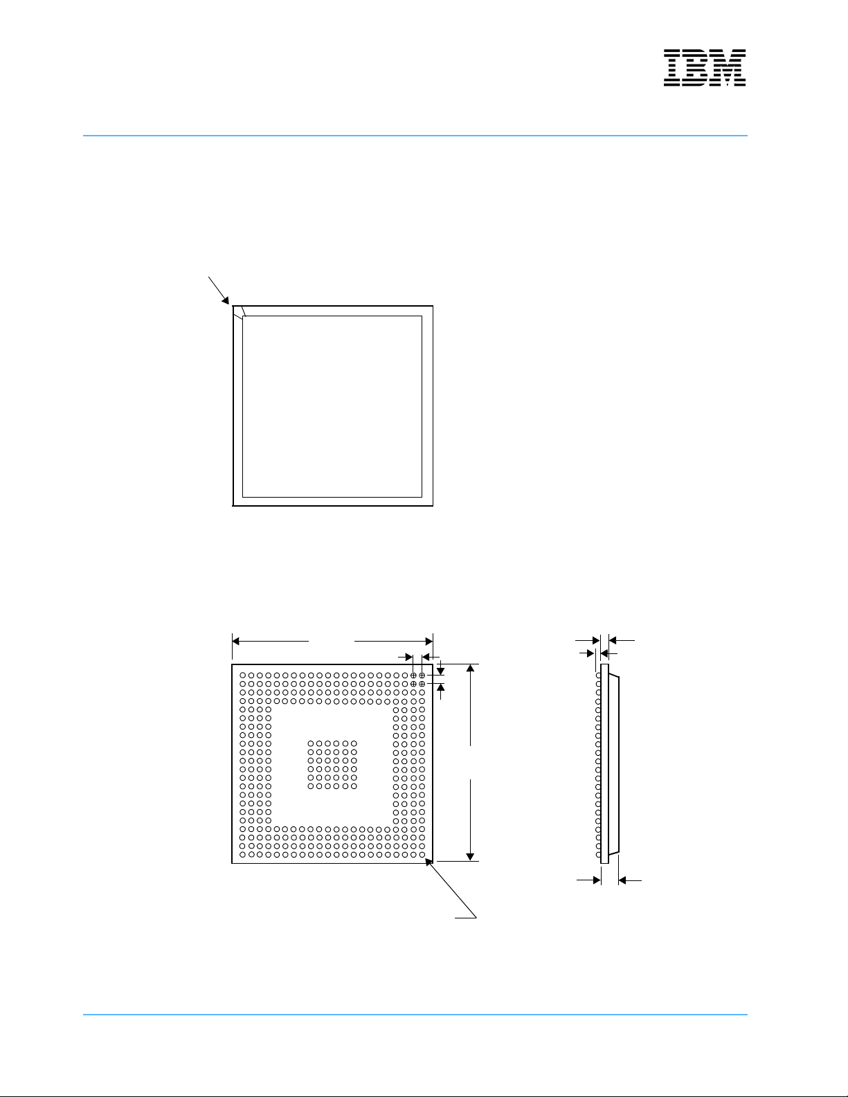
23mm, 324-Ball E-PBGA Package
Top View
Gold gate release
corresponds to
A01 ball location
Bottom View
AB
Y
V
T
P
M
K
H
F
D
B
Note:
All dimensions are in mm.
AA
W
U
R
N
L
J
G
E
C
A
01 03 050709 11 13 15 17
02 04
Thermal balls
0810
06
23.0
12 14
1.0
19
21
20
22
16 18
0.60 Solder Ball
0.60 nom
0.30 nom
1.0
23.0
2.65 max
12

Preliminary
PowerNP NPe405L Embedded Processor Data Sheet
Signal Lists
The following table lists all the external signals in alphabetical order and shows the ball number on which the
signal appears. Multiplexed signals are shown with the default signal (following reset) not in brackets and the
alternate signal or signals in brackets. Multiplexed signals appear alphabetically multiple times in the list—
once for each signal name on the ball. The page number listed gives the page in “Signal Functional
Description” on page 32 where the signals in the indicated interface group begin.
Signals Listed Alphabetically (Part 1 of 11)
Signal Name Ball Interface Group Page
AV
DD
BA0 AB15
BA1 Y14
BankSel0
BankSel1
BankSel2
BankSel3
CAS
ClkEn0 Y13
ClkEn1 AA13
[DMAAck0
[DMAAck1
[DMAAck2
[DMAAck3
[DMAReq0
[DMAReq1
[[DMAReq2
[DMAReq3
DQM0 U03
DQM1 U01
DQM2 R02
DQM3 L01
DQMCB AA04 SDRAM 33
ECC0 AA05
ECC1 Y06
ECC2 AB04
ECC3 AA03
ECC4 Y05
ECC5 AB03
ECC6 Y04
ECC7 W06
EMC0MDClk AB16 Ethernet 32
EMC0MDIO AA16 Ethernet 32
[EMC0Sync]EMC0TxEn[EMC0Tx0En] AB21 Ethernet 32
]GPIO13 U22
]GPIO14 U21
]GPIO15 T20
]GPIO16 D17
]GPIO09 P19
]GPIO10 T22
]GPIO11 T21
]GPIO12 R20
H21 Power 37
SDRAM 33
AA07
Y08
AB06
AA06
AA12 SDRAM 33
SDRAM 33
SDRAM 33
External Peripheral Bus 34
External Peripheral Bus 34
SDRAM 33
SDRAM 33
13

Preliminary
PowerNP NPe405L Embedded Processor Data Sheet
Signals Listed Alphabetically (Part 2 of 11)
Signal Name Ball Interface Group Page
EMC0TxD0[EMC0Tx0D0][EMC0Tx0D] AA22
EMC0TxD1[EMC0Tx0D1][EMC0Tx1D] U19
EMC0TxD2[EMC0Tx1D0] W20
EMC0TxD3[EMC0Tx1D1] Y22
EMC0TxEn[EMC0Tx0En][EMC0Sync] AB21 Ethernet 32
EMC0TxErr[EMC0Tx1En] AB20 Ethernet 32
[EMC0Tx0En]EMC0TxEn[EMC0S ync] AB21
[EMC0Tx1En]EMC0TxErr AB20
[EOT0
/TC0]GPIO24 B19
/TC1]GPIO25 B18
[EOT1
[EOT2
/TC2]GPIO26 C16
/TC3]GPIO27 B17
[EOT3
GND A01
GND A05
GND A09
GND A14
GND A18
GND A22
GND B02
GND B21
GND C03
GND C20
GND D04
GND D08
GND D11
GND D12
GND D15
GND D19
GND E01
GND E22
GND H04
GND H19
GND J01
GND J09-J14
GND J22
GND K09-K14
GND L04
GND L09-L14
GND L19
Ethernet 32
Ethernet 32
External Peripheral Bus 34
Power
Note: J09-J14, K09-K14, L09-L14, M09-M14, N09-
N14, and P09-P14 are also thermal balls.
37
14

PowerNP NPe405L Embedded Processor Data Sheet
Signals Listed Alphabetically (Part 3 of 11)
Signal Name Ball Interface Group Page
GND M04
GND M09-M14
GND M19
GND N09-N14
GND P01
GND P09-P14
GND P22
GND R04
GND R19
GND V01
GND V22
GND W04
GND W08
GND W11
GND W12
GND W15
GND W19
GND Y03
GND Y20
GND AA02
GND AA21
GND AB01
GND AB05
GND AB09
GND AB14
GND AB18
GND AB22
Power
Note: J09-J14, K09-K14, L09-L14, M09-M14, N09-
N14, and P09-P14 are also thermal balls.
Preliminary
37
15
 Loading...