

Page 1

Page 2

CONTENT
1. INTRODUCTION .....................................................................................................1
2.TECHNICAL SPECIFICATION...................................................................................2
3. BLOCK DIAGRAM ..................................................................................................3
4. SCHEMATIC DIAGRAM ...........................................................................................4
5. WIRING DIAGRAM ..................................................................................................6
6. PCB LAYOUT ..........................................................................................................7
7. TEST PROCEDURE .................................................................................................9
8. EXPLODED VIEW & MECHANICAL PARTS LIST ......................................................11
9. BOM ......................................................................................................................13
Page 3

1. INTRODUCTION
- 1 MIC Input channel with gold plated XLR and balanced line inputs
- 2 Stereo input channel with balanced TRS jacks
- Extremely high headroom-offering dynamic range
- Balanced inputs for highest signal interity
- Warm, natural 2-Band EQ on mono channel.
- Warm, natural 2-Band EQ on mono channel.
- Balanced TRS and Headphone Outputs
- 2-track inputs assignable to main mix, headphone output
- Highly accurate 4 segment bar graph meters
- Performance and excellent noise figures
- Manufactures under ISO 9001 certified management system
- 1 -
Page 4
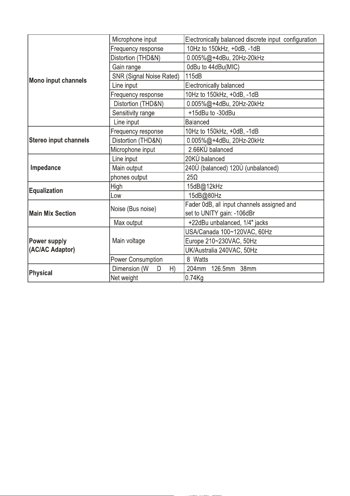
2.TECHNICAL SPECIFICATION
X
XX
X
- 2 -
Page 5
3. BLOCK DIAGRAM
- 3 -
Page 6
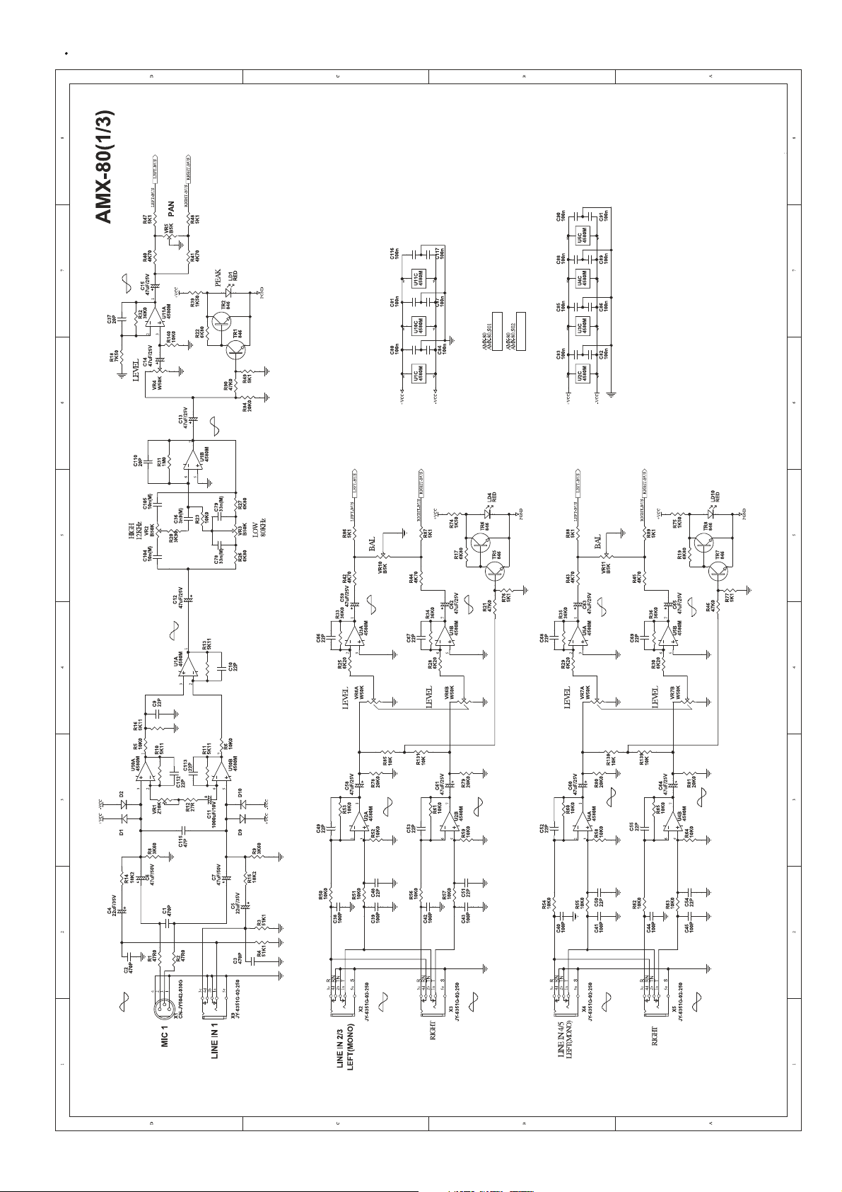
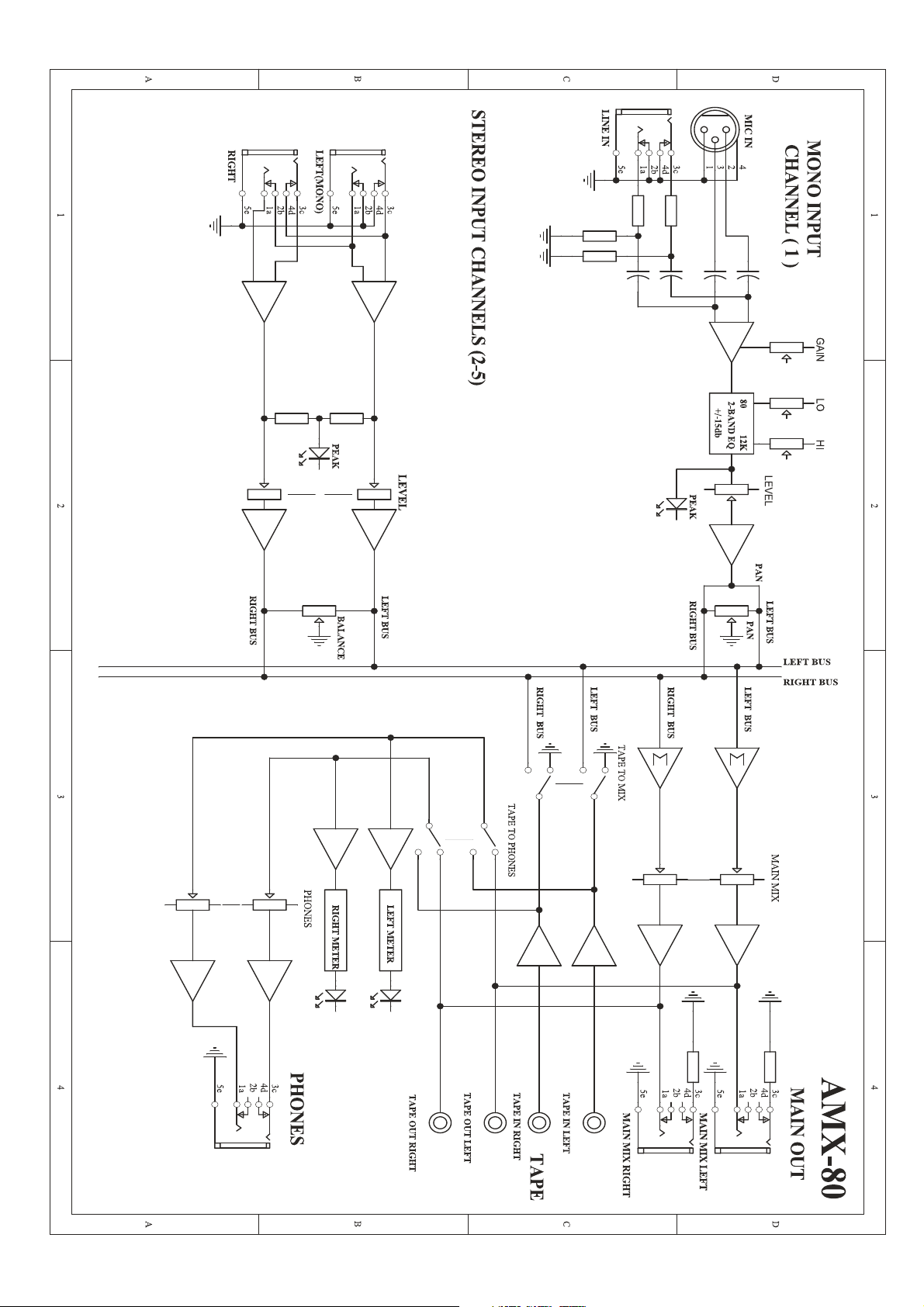
4. SCHEMATIC DIAGRAM
- 4 -
Page 7

- 5 -
Page 8

- 5 -
Page 9

5. WIRING DIAGRAM
- 6 -
Page 10
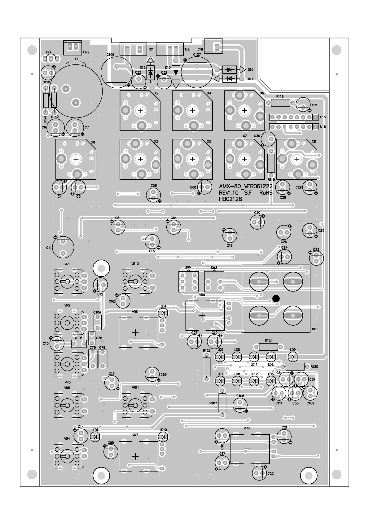
6. PCB LAYOUT
HB02128-AMX-80 TOP LAYER TOP OVERLAY
- 7 -
Page 11

HB02128-AMX-80 BOTTOM LAYER BOTTOM OVERLAY
- 8 -
Page 12

7. AMX-80 TEST PROCEDURE
1. Test instruments:
1). AP ( Audio precision )
2).Dual track oscilloscope
3. Volt meter
2. Instrument setting:
1). AP output : 0dBu 1Khz SINE wave, Load out 40ȍ Bal-Float or Load out 600ȍBNC-Unbal.
2). AP input : Load 100KȍBNC-Unbal or Load 100KȍBal-Float BWΚ22Hz~22KHz. FltrΚ
A-Weighting(1207)
3. Visual Check:
1). Check the AMX-80 surface; and be sure no fri ction of all pots.
4. Functions Test:
1). Set all knob to 0 position, TRIM to minimum , and MAIN MIX LEVEL to middle position.
2). Set AP output to -30 dBu, connecting unbalanced input to LINE IN 1, unbalanced output
to MAIN OUTPUT, then the output LEVEL should be -45dBu(±3dBu)
Set TRIM to maximum, output LEVEL should be 0dBu(±3dBu)
(After test set TRIM back to minimum)
3). Set AP output to +15dBu, connecting unbalanced input to LINE IN 1, unbalanced output to
MAIN OUTPUT, then the output LEVEL should be 0dBu(±3dBu) THD+N<0.005%.
Rotate CH LEVEL to maximum, output LEVEL should be +15dBu (±3dBu)
THD+N<0.005%.
(After test set CH LEVEL back to middle position)
Rotate MAIN MIX LEVEL to maximum, the output LEVEL should be +15dBu (±3dBu)
THD+N<0.008%.
(After test set MAIN MIX LEVEL back to middle position, and CH LEVEL to minimum.)
4). Set AP input to 0dBu, connecting unbalanced input with LINE2/3~LINE4/5, unbalanced
output to MAIN OUTPUT, then the output LEVEL should be 0dBu (±3dBu) THD+N<0.005%.
Rotate CH LEVEL to maximum, the output should be +15dBu (±3dBu) THD+N<0.005%.
(After test set CH LEVEL back to middle position)
5). Set AP input to 0dBu, connecting balanced input to MIC1, and the unbalanced output to
MAIN OUTPUT, then the level should be 0 dBu (±3dBu), THD+N<0.005%. (After test set CH
LEVEL back to middle position)
Set the MAIN MIX LEVEL knob to maximum, the output level should be +15dBu (±3dBu),
THD+N<0.008%. (After test set MAIN MIX LEVEL back to middle position. And set the CH
LEVEL to minimum. )
6). Set AP input to +15dBu, connecting unbalanced input to LINE IN1, and the unbalanced
output to PHONES, the output level should be 0dBu(±3dBu) THD+N<0.01%.
Rotate the CH LEVEL to maximum, output level should be +15dBu (±3dBu),
THD+N<0.006%.( After test set the knob to central position )
Set the MAIN MIX LEVEL to maximum, the output level should be+15dBu (±3dBu),
THD+N<0.01%.( After test set the knob to central position)
- 9 -
Page 13

Set the PHONES to maximum, the output level should be+10dBu (±3dBu), THD+N<0.006%.
( Af ter test set the knob to central position and CH LEVEL to minimum. )
7). Set AP input to 0dBu, connecting unbalanced input at LINE IN2/3~ LINE IN4/5, and the
unbalanced output to PHONES, the output level should be 0dBu(±3dBu) THD+N<0.01%.
Rotate the CH LEVEL to maximum, output level should be +15dBu (±3dBu),
THD+N<0.006%.( After test set the knob to central position )
Set the MAIN MIX LEVEL to maximum, the output level should be+15dBu (±3dBu),
THD+N<0.01%.( After test set the knob to central position)
Set the PHONES to maximum, the output level should be+10dBu (±3dBu), THD+N<0.006%.
( Af ter test set the knob to central position and CH LEVEL to minimum. )
8). Set AP input to +15dBu, connecting u nbalanced input at LINE IN1, and the unbalanced ou tput
to TAPE OUT, the output level should be 0dBu(±3dBu) THD+N<0.005%.
Rotate the CH LEVEL to maximum, output level should be +15dBu (±3dBu),
THD+N<0.005%.( After test set the knob to central position )
Set the MAIN MIX LEVEL to maximum, the output level should be+15dBu (±3dBu),
THD+N<0.008%.
( Af ter test set the knob to central position and CH LEVEL to minimum. )
9). Set AP input to 0dBu, connecting unbalanced input at LINE IN2/3~ LINE IN4/5, and the
unbalanced output to TAPE OUT, the output level should be 0dBu(±3dBu) THD+N<0.005%.
Rotate the CH LEVEL to maximum, output level should be +15dBu (±3dBu),
THD+N<0.005%.( After test set the knob to central position )
Set the MAIN MIX LEVEL to maximum, the output level should be+15dBu (±3dBu),
THD+N<0.008%.
( Af ter test set the knob to central position and CH LEVEL to minimum. )
10). Set AP input to 0dBu, connecting unbalanced input to TAPE IN and the unbalanced output to
MAIN OUTPUT, then press the TAPE TO MIX key ,the output level should be 0dBu(±3dBu)
THD+N<0.005%.
Set the MAIN MIX LEVEL to maximum, the output level should be+15dBu (±3dBu),
THD+N<0.009%. ( After test repeat press the key once )
11). Set AP input to 0dBu, connecting unbalanced input to TAPE IN and the unbalanced output to
TAPE OUT, then press the TAPE T O MIX key ,the output level should be 0dBu(±3dBu)
THD+N<0.005%.
Set the MAIN MIX LEVEL to maximum, the output level should be+15dBu (±3dBu),
THD+N<0.009%. ( After test repeat press the key once )
12). Set AP input to 0dBu, connecting unbalanced input to TAPE IN and the unbalanced output to
PHONES, then press the TAPE TO PHONES key ,the output level should be 0dBu(±3dBu)
THD+N<0.005%.
Set the PHONES control to maximum, the output level should be 10dBu (±3dBu),
THD+N<0.009%. ( After test repeat press the key once )
- 10-
Page 14
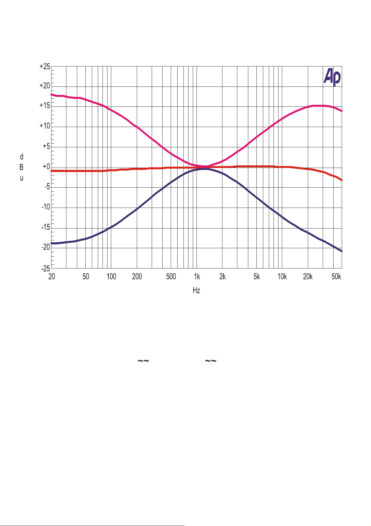
5. Frequency Response test
With unbalance input connecting LINE IN of the AMX-80, set the high EQ knob to maximum & low EQ knob to
minimum(the mid EQ to middle position),and use unbalanced output to connect MAIN OUT. The frequency
response diagram should be as following:
6. Random check
Connect AMX-80 to high quality amplifier and speaker, to check if the sound is normally.
7. The shipment setting of the AMX-80
Set all the volumes knobs to minimum, all the other knobs to middle position, and all the switches
to off position.
Test Complete
- 11 -
Page 15

8. EXPLODED VIEW & MECHANICAL PARTS LIST
- 12-
Page 16

- 12 -
Page 17

9.BOM
Class Part No. Part Name Specification
PF03243
ѥ0001
ѥ0002
ѥ0003
ѥ0004
ѥ0005
ѥ0006
ѥ0007
ѥ0008
ѥ0009
ѥ0010
ѥ0011
ѥ0012
ѥ0013
ѥ0014
ѥ0015
ѥ0016
ѥ0017
ѥ0018
ѥ0019
Ѩ Ѭ0001
ѥ0020
Ѩ Ѭ0001
ѥ0021
Ѩ ѥ0001
Ѩ Ѭ0002
ѥ0022
Ѩ ѥ0001
Ѩ Ѭ0002
ѥ0023
ѥ0024
Ѩ Ѭ0001
ѥ0025
Ѩ Ѭ0001
ѥ0026
ѥ0027
ѥ0028
Ѩ Ѭ0001
ѥ0029
ѥ0030
ѥ0031
ѥ0032
Ѩ ѥ0001
Ѩ ѥ0002
Ѩ ѥ0003
Ѩ ѥ0004
Ѩ ѥ0005
Ѩ ѥ0006
MA06128
MB04892
HI00171
NI02084
NI02817
NI02082
NI02083
NI00826
NI02837
NI02377
MG00041
MG00061
ME00060
MF00061
NA00121
NB04908
NB04909
NF00061
NE05004
NH00334
NF02625
NH00149
NE16344
NI00014
NH00012
NE02717
NH00038
NI00028
TG00212
NI00245
NI00243
NI00261
NI00258
HC00839
NI00378
NC00037
NC01110
NI00498
HA00040
HA01551
HK07192
CB00073
HC00076
SD00077
SD00079
RC00358
RC00465
MIXER AMX-80_ALTO_230V 1
panle-RS AMX-80 ALTO_V1.3 1
chassis-RS AMX-80 ALTO_V1.2 1
power switch-RS R612KKAT0F1 1
knob ij10.5*18mm 1
knob ij10.5*18mm 1
knob ij10.5*18mm 3
knob ij10.5*18mm 2
knob ij12*18mm double color 3
knob ij35*11mm 534C 1
knob-RS ij5.5*7.5(3.3*3.3mm)_V1.2 2
screw
M3*6 13
screw-RS M3*10 3
MIC jack JY-6351G-02-250 8
MIC jack ij9.6*ij13*0.5t 9
PE bag
0.04t*280*220mm 1
gift carton-RS AMX-80 ALTO_V1.1 1
barrier-RS AMX-80_V1.2 1
assurance card
ALTO 1
label ALTO 4
cone paper 0.040*1m 1
user manual-RS AMX-80 ALTO_V1.0 1
paper 889*640mm
lable-RS AMX-80_V1.0 4
membrane
bond paper
0.035*1M 1
0.04*1M 1
label MADE IN CHINA 2
paper 0.115*1M 1
membrane
adaptor-RS
sleeve
sleeve
sleeve
sleeve
0.110*1M 1
230V/50Hz_AC18V/500mA_EI-41_CE
ij3*10mm 3
ij3*1000mm 10
ij5*20mm 2
ij5*1000mm 20
DC power jack-RS SCD554CCS103BB4G 1
plastic washer 9*13 used to PU socket 1
cushion-RS-ACT 1t*ij8*ij12.5mm XM1602_V1.1 1
insulator 1.0t*65mm(+0.1)*60M 0.3
self-adhere foot cushion 12.7*7*6mm(SF-005) 4
wire-RS 60mm yellow L5R5 1
wire-RS 2P 80mm UL1007 26AWG 1
PC board-RS P-AMX-80-DIP 1
electrolytic capacitor 1000uF/35V ij13*20mm 2 C106,C107
connector(male) 2P 2.5mm 180° 1 CN1
integrated circuit-RS L7815CV(TO220)/(ST/MOROCCO) 1 IC1
integrated circuit L7915CV(TO220)/(ST) 1 IC2
potentiometer
potentiometer
B50Kȍ-RD09F113A223-50K2BT(SAS1);30F-C
B5Kȍ RD09F113A225-5K2BT(SAS1);30F-C
QTY
Remark
0.75
1
2 VR2,VR3
3 VR5,VR10,VR11
-13 -
Page 18

Class Part No. Part Name Specification
,
,
Ѩ ѥ0007
Ѩ ѥ0008
Ѩ ѥ0009
Ѩ ѥ0010
Ѩ ѥ0011
Ѩ ѥ0012
Ѩ ѥ0013
Ѩ ѥ0014
Ѩ ѥ0015
Ѩ ѥ0016
Ѩ ѥ0017
Ѩ ѥ0018
Ѩ ѥ0019
Ѩ ѥ0020
Ѩ Ѩ Ѭ0001
Ѩ ѥ0021
Ѩ ѥ0022
Ѩ ѥ0023
Ѩ ѥ0024
Ѩ ѥ0025
Ѩ ѥ0026
Ѩ ѥ0027
Ѩ ѥ0028
Ѩ Ѩ ѥ0001
Ѩ Ѩ ѥ0002
Ѩ Ѩ ѥ0003
Ѩ Ѩ ѥ0004
SD00007
HC00126
SA00052
HC00125
HI00236
SA00053
HC00528
RC00359
RC00361
RC00617
SA00054
RC00356
NI01782
MI02702
MJ00055
ME00015
MF00037
MG00162
NI02249
NC00005
ND00155
AC00179
HK07193
SE00011
RD00224
CI00059
CI00075
integrated circuit
balance MIC jack-RS JY-5042-030G female plug 180° 1 X1
L.E.D ij3 round(green)long foot 26 5 LD5,LD6,LD7,LD8,LD9
MIC jack-RS JY-6351G-02-250 8 X2,X3,X4,X5,X6,X7,X8,X9
push-button switch-RS 2 6P PS-92 26A(SELF-LOCK) 2 SW3,SW4
L.E.D ij3 round(red)long foot 26mm 5 LD1,LD2,LD3,LD4,LD10
RCA jack SCP6873NS3232T1 4P red white 1 X10
potentiometer
potentiometer
potentiometer(dual unit)-RS
L.E.D
potentiometer
LED spacer support LEDS-11 11mm 12
bady-RS-ACT MIX50 2t*29*35*39_V1.0 1
AL plate 2*2000*1000 10.88kg 1
color nut 3m/m 2
washer ij3.2*ij5.5*1t 2
screw
plastic washer TW-1(TO-220) 2
mica SB-9500DSP 18*13*0.1t_V1.0 2
EV foam 25*20*5 1
tin without lead-RS M705E Sn 3Ag-0.5Cu
PC board-RS P-AMX-80-SMD 1
SMD rectifier diode
SMD precise resistor 1/10W
SMD ceramic capacitor 0603
SMD ceramic capacitor 0603
BA15218N(use M5218Linstead )(SIP8)/(ROHM)
W50Kȍ RD09F113A224-50K4BT(SAS1);30F-C
W50Kȍ RD12L12CA60B-50K4BT*2(SAS1);30F-C
W50Kȍ RD12L12CA606-50KBT*2(SAS);20F-C
3m/m round(yellow)long foot 26
Z10Kȍ RD09F1130042-10KZ(SAS1);30F
M3*8 2
RLS4148 0.5A (LL-34) 8
100Kȍ ±1% 0603 4 R132,R133,R134,R135
100PF/50V NPO ±5% 10
0.1uF/50V Y5V +80,-20%
QTY
Remark
2 U15,U16
1 VR4
3 VR6,VR7,VR9
1 VR8
2 LD11,LD12
1 VR1
9.5148
D1,D2,D3,D4,D5,D6,D9,D10
C38,C39,C40,C41,C42,
C43
C44,C45,C46,C47
C80,C81,C82,C83,C84,
C85,C86,C87,C88,C89,
C90,C91,C92,C93,C94,
27
C95,C96,C97,C98,C99,
C100,C101,C102,C103,
Ѩ Ѩ ѥ0005
Ѩ Ѩ ѥ0006
Ѩ Ѩ ѥ0007
Ѩ Ѩ ѥ0008
Ѩ Ѩ ѥ0009
Ѩ Ѩ ѥ0010
Ѩ Ѩ ѥ0011
Ѩ Ѩ ѥ0012
Ѩ Ѩ ѥ0013
Ѩ Ѩ ѥ0014
RD00214
RD00272
RD00275
RD00069
RD00200
RD00282
RD00201
RD00292
RD00219
CI00109
SMD precise resistor 1/10W
SMD precise resistor 1/10W
SMD precise resistor 1/10W
10.0Kȍ ±1% 0603 37
10.0ȍ ±1% 0603 1 R125
110ȍ ±1% 0603 1 R126
SMD fixed resistor 1/10W 120ȍ ±5% 0603 8
SMD precise resistor 1/10W
SMD precise resistor 1/10W
SMD precise resistor 1/10W
SMD precise resistor 1/10W
SMD precise resistor 1/10W
SMD ceramic capacitor 0603
150ȍ ±1% 0603 1 R127
1.00Kȍ ±1% 0603 3 R110,R111,R128
1.50Kȍ ±1% 0603 3 R39,R74,R75
1.00Mȍ ±1% 0603 1 R31
20.0Kȍ ±1% 0603 9
20PF/50V C0G±5%(C1608C0G1H200JT)/TDK
- 14 -
R5,R6,R7,R23,R50,R51,R52,
R53,R54,R55,R56,R57,R58,
R59,R60,R61,R62,R63,R64,
R65,R66,R67,R68,R69,R70,
R71,R72,R73,
R136,R137,R140,R85,R131,
R138,R139,R14,R15
R99,R100,R101,R102,
R103
R104,R105,R106
R78,R79,R80,R81,R82,R8
3,R84,R91,R92
2 C37,C110
Page 19

Class Part No. Part Name Specification
,
Ѩ Ѩ ѥ0015
Ѩ Ѩ ѥ0016
Ѩ Ѩ ѥ0017
Ѩ Ѩ ѥ0018
Ѩ Ѩ ѥ0019
Ѩ Ѩ ѥ0020
Ѩ Ѩ ѥ0021
Ѩ Ѩ ѥ0022
Ѩ Ѩ ѥ0023
Ѩ Ѩ ѥ0024
Ѩ Ѩ ѥ0025
Ѩ Ѩ ѥ0026
Ѩ Ѩ ѥ0027
Ѩ Ѩ ѥ0028
Ѩ Ѩ ѥ0029
Ѩ Ѩ ѥ0030
Ѩ Ѩ ѥ0031
Ѩ Ѩ ѥ0032
Ѩ Ѩ ѥ0033
Ѩ Ѩ ѥ0034
Ѩ Ѩ ѥ0035
Ѩ Ѩ ѥ0036
Ѩ Ѩ ѥ0037
Ѩ Ѩ ѥ0038
Ѩ Ѩ ѥ0039
Ѩ Ѩ ѥ0040
Ѩ Ѩ ѥ0041
Ѩ Ѩ ѥ0042
Ѩ Ѩ ѥ0043
Ѩ Ѩ Ѩ ѥ0001
Ѩ Ѩ Ѩ ѥ0002
Ѩ Ѩ Ѩ ѥ0003
Ѩ Ѩ Ѩ ѥ0004
Ѩ Ѩ Ѩ ѥ0005
Ѩ Ѩ Ѩ ѥ0006
Ѩ Ѩ Ѩ ѥ0007
Ѩ Ѩ Ѩ ѥ0008
Ѩ Ѩ Ѩ ѥ0009
Ѩ Ѩ Ѩ ѥ0010
Ѩ Ѩ Ѩ ѥ0011
Ѩ Ѩ Ѩ ѥ0012
Ѩ Ѩ Ѩ Ѭ0013
CI00051
RD00106
RD00265
RD00203
RD00329
RD00370
RD00407
SF00053
RD00406
RD00414
CI00063
RD00078
RD00339
CI00055
RD00298
RD00341
RD00371
RD00094
RD00210
RD00211
RD00510
RD00326
RD00082
SF00033
RD00327
SE00008
SG00116
RD00213
HK07170
HB02128
CC00074
RA01260
SA00159
SA00328
CB00242
CC00059
CC00063
RA01259
CB00194
CB00334
HA01933
RA01413
SMD ceramic capacitor 0603
SMD fixed resistor 1/10W 27Kȍ ±5% 0603 2 R116,R117
SMD fixed resistor 1/10W 27ȍ ±5% 0603 1 R12
SMD precise resistor 1/10W
SMD precise resistor 1/10W
SMD precise resistor 1/10W
SMD precise resistor 1/10W
transistor MMBT3906(SOT23)/(PHI) 2 TR3,TR4
SMD precise resistor 1/10W
SMD precise resistor 1/10W
SMD ceramic capacitor 0603
SMD fixed resistor 1/10W 470ȍ ±5% 0603 2 R123,R124
SMD precise resistor 1/10W
SMD ceramic capacitor 0603
SMD precise resistor 1/10W
SMD precise resistor 1/10W
SMD precise resistor 1/10W
SMD fixed resistor 1/10W 5.1Kȍ ±5% 0603 9
SMD precise resistor 1/10W
SMD precise resistor 1/10W
SMD precise resistor 1/10W
SMD precise resistor 1/10W
SMD fixed resistor 1/10W 820ȍ ±5% 0603 1 R129
SMD transistor-RS-ACT BC846B(SOT23)/(PHI) 6
SMD precise resistor 1/10W
SMD rectifier diode
SMD integrated circuit
SMD precise resistor 1/10W
PC board-RS P-AMX-80-AI 1
PCB-RS AMX-80_VER061222 1
mylar capacitor-RS-ACT 0.01uF/100V 3% 2 C104,C105
fixed resistor 1/4W 120ȍ 2 R107,R122
rectifier diode 1A/1000V IN4007 2 D14,D15
Schottky barrier diode-RS 1N5817(DO-41) 2 D12,D13
electrolytic capacitor 22uF/35V ij5*11mm 2 C4,C5
mylar capacitor 0.033uF/100V 3% 2 C78,C79
mylar capacitor-RS 0.0039uF/100V 10% 1 C36
fixed resistor 1/4W 47ȍ 4 R118,R119,R120,R121
electrolytic capacitor 47uF/25V ij5*11mm 36
electrolytic capacitor-RS 47uF/50V ij6.3*11mm 2 C6,C7
jump 2.5mm 1 CN2
fixed resistor 1/4W 2.7Kȍ 2 R141,R142
22PF/50V C0G±5%(C1608C0G1H220JT)/TDK
2.00Kȍ ±1% 0603 1 R130
30.0Kȍ ±1% 0603 4 R93,R94,R95,R96
33.2Kȍ ±1% 0603 2 R37,R38
36.0Kȍ ±1% 0603 5 R32,R33,R34,R35,R36
3.60Kȍ ±1% 0603 4 R8,R9,R97,R98
3.90Kȍ ±1% 0603 1 R20
470PF/50V NPO ±5н
47.0Kȍ ±1% 0603 3 R21,R46,R90
47PF/50V C0G±5%(C1608C0G1H470JT)/TDK
47.0ȍ ±1% 0603 2 R1,R2
4.70Kȍ ±1% 0603 6
51.1Kȍ ±1% 0603 2 R3,R4
5.11Kȍ ±1% 0603 6
5.49Kȍ ±1% 0603 2 R112,R113
6.20Kȍ ±1% 0603 4 R25,R28,R29,R30
6.80Kȍ ±1% 0603 5 R17,R19,R22,R26,R27
8.20Kȍ ±1% 0603 2 R108,R109
DA204K/T-146 1 D7
BA10339FV E2(SSOP-B14)/(ROHM)
7.50Kȍ ±1% 0603 1 R18
QTY
Remark
C9,C10,C48,C49,C50,C51,
C52,C53,C54,C55,C56,C57,
C66,C67,C68,C69,C70,C71,
26
C72,C73,C74,C75,C76,C77,
C112,C113
3 C1,C2,C3
1 C115
R40,R41,R42,R43,R44,R45
R47,R48,R49,R76,R77,
R86
R87,R88,R89
R10,R11,R13,R16,R114,R115
TR1,TR2,TR5,TR6,TR7,TR8
2 U13,U14
C8,C12,C13,C14,C15,C16,C17,C
18,C19,C20,C21,C22,C23,
C24,C25,C26,C27,C28,C29,
C30,C31,C32,C33,C34,C35,
C58,C59,C60,C61,C62,C63,
C64,C65,C108,C109,C111
- 15 -
Page 20

Class Part No. Part Name Specification
,U9,
Ѩ Ѩ Ѭ0044
Ѩ ѥ0029
Ѩ Ѭ0030
ѥ0033
Ѭ0034
SG00558
CB00255
SD00238
HJ00002
NB04919
integrated circuit-RS 4580M(SOP8)/(YW) 12
electrolytic capacitor 1000uF/10V ij8*11mm 5mm 1 C11
integrated circuit MC78L18ACP(TO92)/(ON) 1 IC3
dessicant 10g 1
carton-RS AMX-80 ALTO_V1.1 1
QTY
Remark
U1,U2,U3,U4,U5,U6,U7,U
8
U10,U11,U12
- 16 -
 Loading...