

Page 1

Service Manual
Model: αCOMP
24x32 Bit Digital Compressor Module
www.altoproaudio.com
Version: 1.1
Page 2

CONTENTS
1. Specification
2. Block Diagram
3. Schematic Diagram
4. Printed Circuit Board
5. Wiring Diagram
6. Test Procedure
7. Electrical Parts List
8. Exploded Views & Mechanical Parts List
9. Notes
Page 3

1. SPECIFICATION (aCOMP)
Electrical
Frequency Response: +0.5 / -1.5 dB from 20Hz to 20 kHz
S/N Ratio (process) 80 dB "A" wtg, 20 Hz-22kHz
S/N Ratio (bypass) >90 dB "A" wtg, 20 Hz-22kHz
THD+Noise: <0.008% @ 1kHz (0dBV, bypass)
Input
Number of Channels: 2
Format: 1/4" unbalanced
Maximum Level (bypass): +9 dBu
Impedance: >500 Kohms
A/D - D/A Conversions
A/D converter: 1 bit Sigma-Delta
D/A converter: 1 bit Sigma-Delta
Output
Number of Channels: 2
Format: 1/4" unbalanced
Maximum Level (bypass): +9 dBu
Output Impedance: <500 ohms
Front Panel
Controls Input/Output Levels (ANALOG)
PROGRAM selections (2 knobs)
Indicators Power, Signal clip LED
Rear Panel
IN/OUT levels (ANALOG) 1/4" 2-conductor (mono)
Output (LEFT, RIGHT) 1/4" 2-conductor (mono)
BYPASS 1/4" 2-conductor (auto-sense pedal type)
for momentary footswitches
Power 9 Volt AC Power Transformer
Processing and Memory
Processor Speed: 12 MIPs (million instructions per second)
Internal DSP resolution: 52 bit MPY accumulator
Main Preset Programs 16
Preset Total Combinations 256
Internal digital audio memory: 3000 milliseconds
Physical
Net Weight: 1kg(2.20lb)
Dimension(WxDxH): 200(mm) 150(mm) 45(mm)
(7.87" x 5.91"x 1.77")
Page 4
D
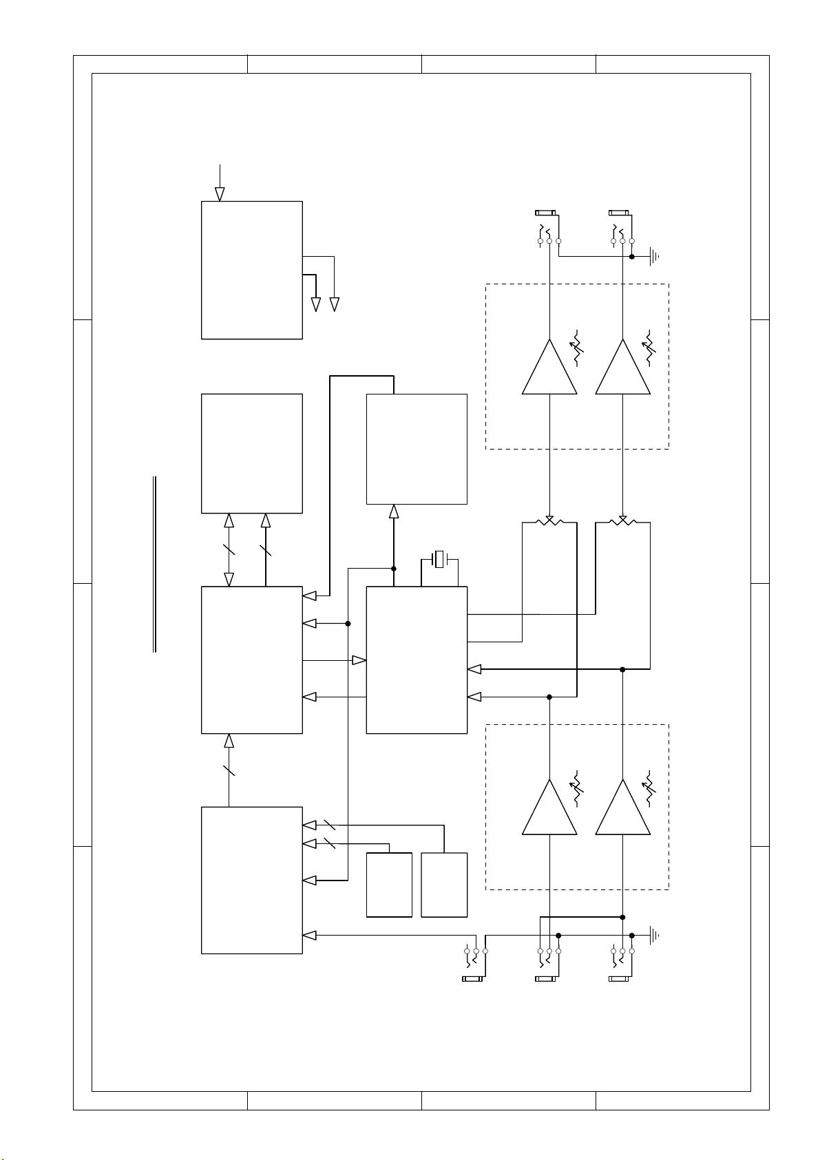
2. Block Diagram
AC 9V
INPUT
C
B
A
4
PJ3
OUTPUT R
OUTPUT L
PJ4
POWER SU PPLY
VOLTAG E REGULATOR
-5V
+5V
LRCKIN=43.20KHZ
BCK=1.382MHZ
OUTPUT LEVEL
OUTPUT LEVEL
OUTPUT AMPLIF IER
321
( U10,U11 )
MEMORY (DRAM)
ED0-ED7
EA0-EA9
CLOCK DIVIDE
( U7 74HC393 )
Q1
11.0592MHZ
11.0592MHZ
MIX CONTROL
alphaverb BLOCK DIAG RA M
( U8 TMS57002DPHA )
( U9 P87C54UBAA )
SO0SI0
( U6 PCM3001E )
STEREO AUD IO C O D EC
A/D and D/A CO N VERT ER
IN-R IN-L OUT-R OUT-L
INPUT LEVEL
INPUT LEVEL
INPUT BUFF ER & AM PLIFIER
PROG RAM
ENCODER A
CONTROL
FOOTSWITCH
ENCODER B
VARIATIONS
PJ5
FOOT
PJ1
SWITCH
INPUT R
PJ2
INPUT L
(MONO INPUT)
1 2 34
DSP
AD0-AD7
MPU
D
C
B
A
Page 5
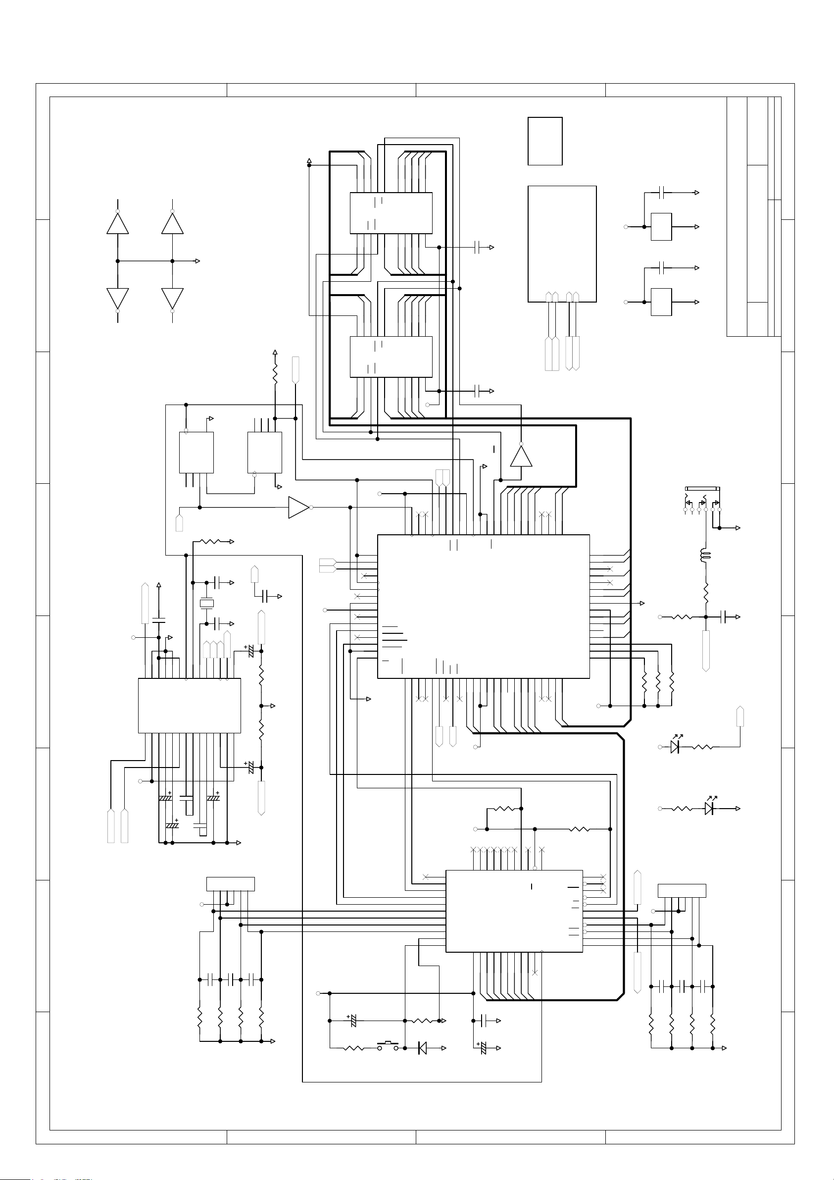
D
3. Schematic Diagram
C
B
A
2002/01/06
8
DGND
ED6
ED7
23
22
25
26
EA8
18
EA7
EA6
EA5
EA4
LINK
LINK.SCH
C99
100nF
KEVIN LIN.
89
U10
U11C
74HC04D
5 6
7654321
U11E
74HC04D
10 11
U11D
74HC04D
DGND
U11F
74HC04D
12 13
DGND
GM71C4256BJ60
ED4
26
U9
R18
100R
LRCKIN
GM71C4256BJ60
ED0
1
CLK
U6A
74HC393D
Q03Q14Q25Q3
BCK
DGND
Q1
C95 100nF
RS-CODEC
+5V
28
11.0592MHz
DGND
22
24
23
VDD
FMT225FMT126FMT027RSTB
CLKIO
DGND
U5
PCM3001E
VINL1VCC12AGND13VREFL4VREFR5VINR6CINPR7CINNR8CINLN9CINPL10VCOM11VOUTR12AGND213VCC2
2
DGND
MR
U6B
6
CLK-Q3
R17
4K7
DGND
22P
C33
DGNDDGND
C32
22P
VOUTL
LRCKIN
SI0
BCK
SO0
19
17
21
20
XTI
XTO
15
18
DIN
DOUT
LRCIN16BCKIN
VOUTL
14
Q011Q110Q29Q3
74HC393D
CLK
13
SO0
OUTPUTLOUTPUTR
C31
1uF
R29
100K
R30
100K
8
LRCKIN
MR
12
DGND
12
U11A
C45
82P
DGND
AGND
74HC04D
+5V
BCKI
SI1
SI0
STRB
CLOAD
PLOAD
OE
I/0224I/03
CAS
DGND
I/001I/012WE3RAS4A95A09A110A211A312+5V
ED5
EA9
EA0
ED2
ED3
25
DGND
I/001I/012WE3RAS4A95A09A110A211A312+5V
ED1
EA8
23
22
18
OE
I/0224I/03
CAS
EA0
EA9
+5V
SYNC
80
SI1
79
SI0
78
NC
77
LRCKI
76
BCKI
75
NC
74
VSS
73
VCC
72
NC
71
STRB
70
69
68
67
R/W
66
CS
65
DGND
VOUTR
+5V
C30
1uF
A414A515A616A717A8
147
C96
100nF
13
EA1
EA2
EA3
EA4
EA5
EA6
EA7
A414A515A616A717A8
13
+5V
EA1
EA2
EA3
CAS
SO0
SO1
7
9
S006S01
OVM
10
CAS8RAS
CLKSEL
AD7
BIO
1
5
4
2
NC3NC
BCK0
LRCK0
SYPOL
CLOAD
DREADY
PLOAD
64
MUTE
EMPTY
RS
11
AD6
+5V
C97
CLKIN
U7
100nF
13
VSS12VSS
TMS57002
DGND
14
WE
AD5
DGNDDGND
a-verbIO.SCH
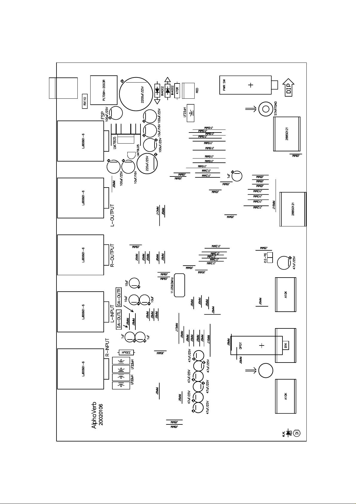
Analog Stage & Power supply
WE
WE
U11B
74HC04D
3 4
ED2
ED3
ED4
ED5
ED6
ED7
ED715ED616ED517ED418ED319ED220ED1
AD3
AD4
NC21NC
AD0
AD1
AD2
INPUTR
INPUTL
OUTPUTR
OUTPUTL
+5V +5V
INPUTL
INPUTR
OUTPUTL
OUTPUTR
ED0
ED1
23
24
22
ED0
EA0
25
EA9
EA8
EA1
NC
EA2
NC
EA3
EA4
VSS
VCC
EA5
EA6
NC
EA7
TEST0
TEST1
TEST2
EA841EA942NC43NC44D045D146D247D348NC49D450D551VCC52VCC53D654D755PC056BIO57OVFA58OVFM59RS60NC61NC62EMPTY63MUTE
+5V
EA0
26
EA1
27
28
EA2
29
30
EA3
31
EA4
32
33
EA5
34
35
EA6
36
37
EA7
38
39
40
U6C
74HC393D
C98
100nF
147
U11G
74HC04D
PJ5
DGND
+5V
R40 0R0
R39 0R0
R38 0R0
+5V
DL1
LJB0661-6
213
R2
10K
RED
(OVER-LOAD)
221133
L9
DGNDDGND
DGND DGND
A-VERBMAIN.SCH
Number RevisionSize
MODEL:ALTO AlphaVERB
Title
FSP
BLM21A102
R3
1K
C7
100nF
Footswitch live
R1
220R
A3
Date: 8-Jan-2002 Sheet of
File: D:\shung\PC27\ALTO\Digital\AlfaVerb\ SCHPCB\alphaverb.ddbDrawn By:
AGND2
DGND
OVM
C38 10uF
C36 470P
C37
C35
10uF
INPUTL
INPUTR
470P
+5V
ENCODERA4
C34
D3
D2
12345
ENCODERA3
C39
100nF
R28
4K7
10uF
COM
C40
R27
D1
COM
ENCODERA2
100nF
4K7
R37
+5V
AGND
D0
6
ENCA
288S0121
ENCODERA1
C41
R26
100nF
4K7
R25
4K7
DGND
+5V
C27
R31
47uF/25V
100R
JP2
2P-2.5
U8
P87C54UBAA
(AlphaComp:P87C52UBAA)
1
2
3
4
5
6
7
8
9
22
10
RST
R24
100K
25
NC
P 1.0
P 1.1
P 2.0/A824P 2.1/A9
P 1.2
P 1.3
P 1.4
P 1.5
P 1.6
P 1.7
VSS
RST
VDD
43
44
AD0
C28
100nF
DGND
C29
1uF
DGND
D4
1N4148
10K
P 2.2/A1026P 2.3/A1127P 2.4/A1228P 2.5/A1329P 2.6/A1430P 2.7/A15
AD1
AD2
AD3
AD4
DGND DGND
A15
35
34
31
NC23NC
EA/VPP
P 0.7/AD736P 0.6/AD637P 0.5/AD538P 0.4/AD439P 0.3/AD340P 0.2/AD241P 0.1/AD142P 0.0/AD0
XTAL121XTAL2
20
AD5
AD6
AD7
R36
ALE
PSEN
NC
RD/P3.7
WR/P3.6
T1/P3.5
T0/P3.4
INT1/P3.3
INT0/P3.2
TXD/P3.1
RXD/P3.0
10K
33
32
12
19
18
17
16
15
14
13
11
F11.0592M
+VCC
DL2
1/4W
470R
D1
COM
ENCODERB2
100nF
4K7
D0
6
C44
R33
RED
ENCB
ENCODERB1
100nF
4K7
R44
D3
D2
COM
12345
RS-CODEC
+5V
ENCODERB4
C42
R35
ENCODERB3
100nF
4K7
C43
R34
Footswitch live
(PWR ON)
288S0121
R32
DGND
4K7
DGND
1 2 3 4 5 6 78
D
C
B
A
Page 6
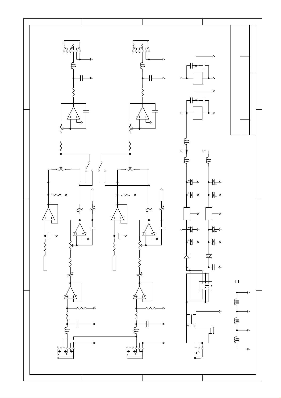
D
C
B
A
R-OUT
PJ3
LJB0661-6
213
221133
C14
AGND
10nF
2
AGND2
AGND
C48
47P
SW2
DPDT
UP=compressor effect
DOWN=bypass
4
VR3A
321
U4A
A10K
R11
AS4
TL074CD
OUTPUT-A
4K7
L1
LF22uH
R20
270R
1
3
2
B1K
VR2A
MIXER-A
PJ4
AS3
U4B
TL074CD
VR3B
A10K
OUTPUT-B
R19
4K7
LJB0661-6
213
VR2B
221133
L6
R23
LF22uH
6
B1K
270R
7
MIXER-B
L-OUT
2002/01/06
KEVIN LIN.
330uH
C21
C19
AGND
100nF
AGND
100nF
-5V -5V
MODEL:ALTO AlphaVERB
Title
A-VERBIO.SCH
Number RevisionSize
AlphaVerb Analog Stage/Power Supply (Included AlphaComp)
A4
Date: 8-Jan-2002 Sheet of
File: D:\shung\PC27\ALTO\Digital\AlfaVerb\SCHPC B\alphaverb.ddbDrawn By:
C20
411
C18
411
+5VA +5VA
L7
BLM21A102
+5V
L2
LF22uH
100nF
U4E
100nF
U1E
TL074CD
TL074CD
-5VSGND
L3
AGND2
AGND
C26
10nF
C49
47P
AGND
5
R21
U4C
R6
10K
(opt alfacomp)
TL074CD
10
AS5
2K2
OUTPUTR
8
9
C23
PJ1
680P
LJB0661-6
U1D
AGND
VR1A
A10K
R7
1K
U1A
TL074CD
3
R4
1K
L4
LF22uH
2132211
33
AGND
C13
TL074CD
INTPUT-A
1
2
47uF/25V
13
C12
C9
14
12
47uF/25V
AS2
R5
220P
1
354
6
C5
10uF/16V
C3
100uF/25V
C15
47uF/25V
47P
U2 LM7805
C1
+VCC
C47
C10
2200uF/25V
D2
IN4002
AGND
AGNDAGND2
61
L10
PLT09H-2003R
INPUTR
C8
47uF/25V
C46
47P
AGND
AGND
1M
AGNDAGND2
R14
U4D
2K2
14
TL074CD
12
AS6
OUTPUTL
13
C24
PJ2
680P
LJB0661-6
R22
10K
(opt. alfacomp)
U1C
AGND
VR1B
A10K
INTPUT-B
R15
1K
U1B
TL074CD
5
R12
1K
L5
LF22uH
2132211
33
AGND
C17
47uF/25V
TL074CD
7
6
INPUTL
8
9
C25
C16
10
47uF/25V
AS1
R13
220P
AGND
1M
3 4
100uF/25V
-5VO
SGNDSGNDSGND
C6
10uF/16V
C4
100uF/25V
U3 LM79L05
C2
SGND
SGND
100uF/25V
C11
SGND SGND SGND SGND
220uF/25V
D3
IN4002
C22
100nF
SGND
1
3
2
SW1
PWR SW
456
P1
STARTGND
AGND2AGND
L8
BLM21A102
SGND
L12
BLM21A102
PS1
RX110
SGND
1 2 3 4
L11
BLM21A102
J1
DGND
R-INPUT
D
C
L-INPUT
(MONO IN)
B
AC 9V INPUT
A
Page 7
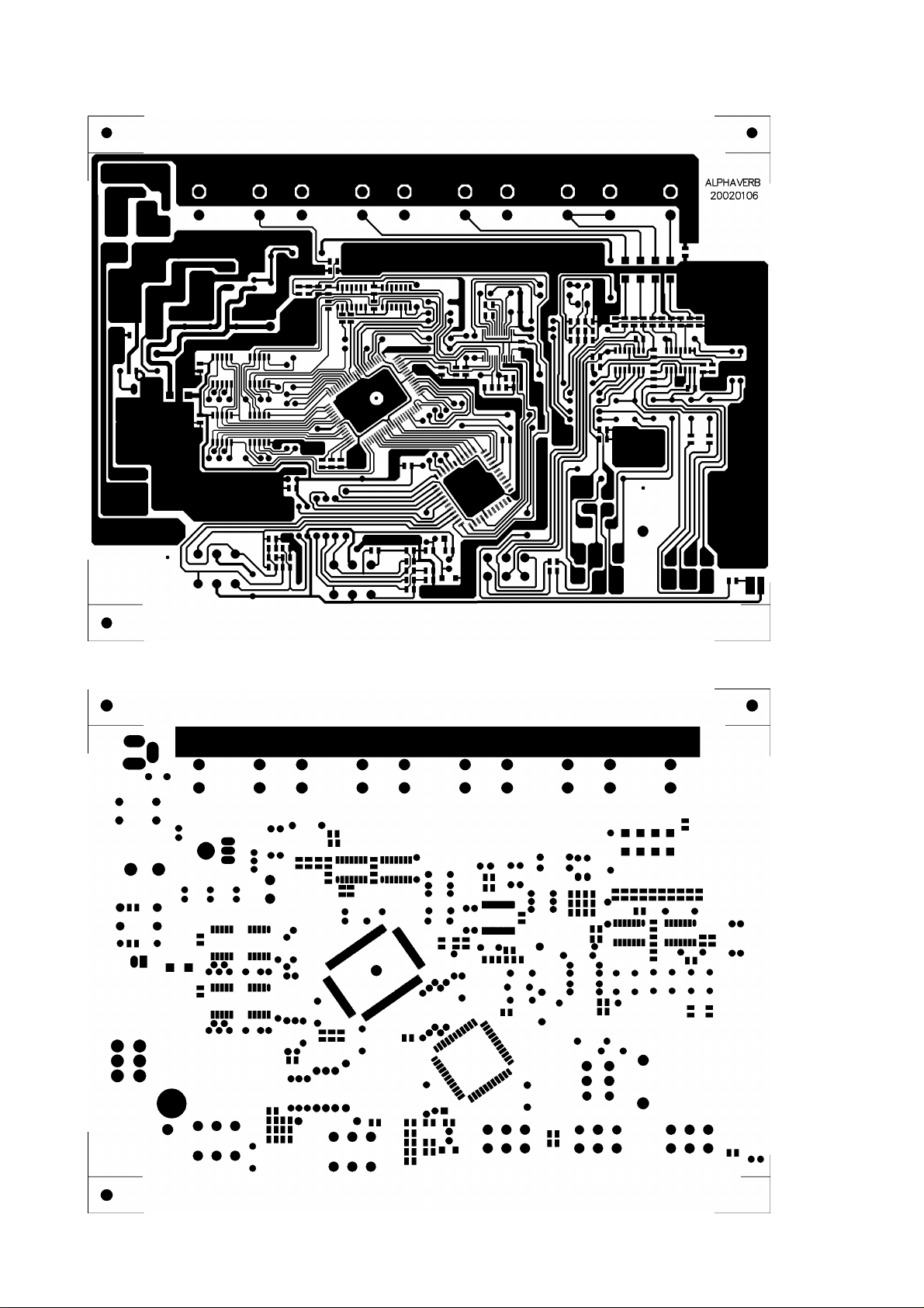
BOTTOM LAYER
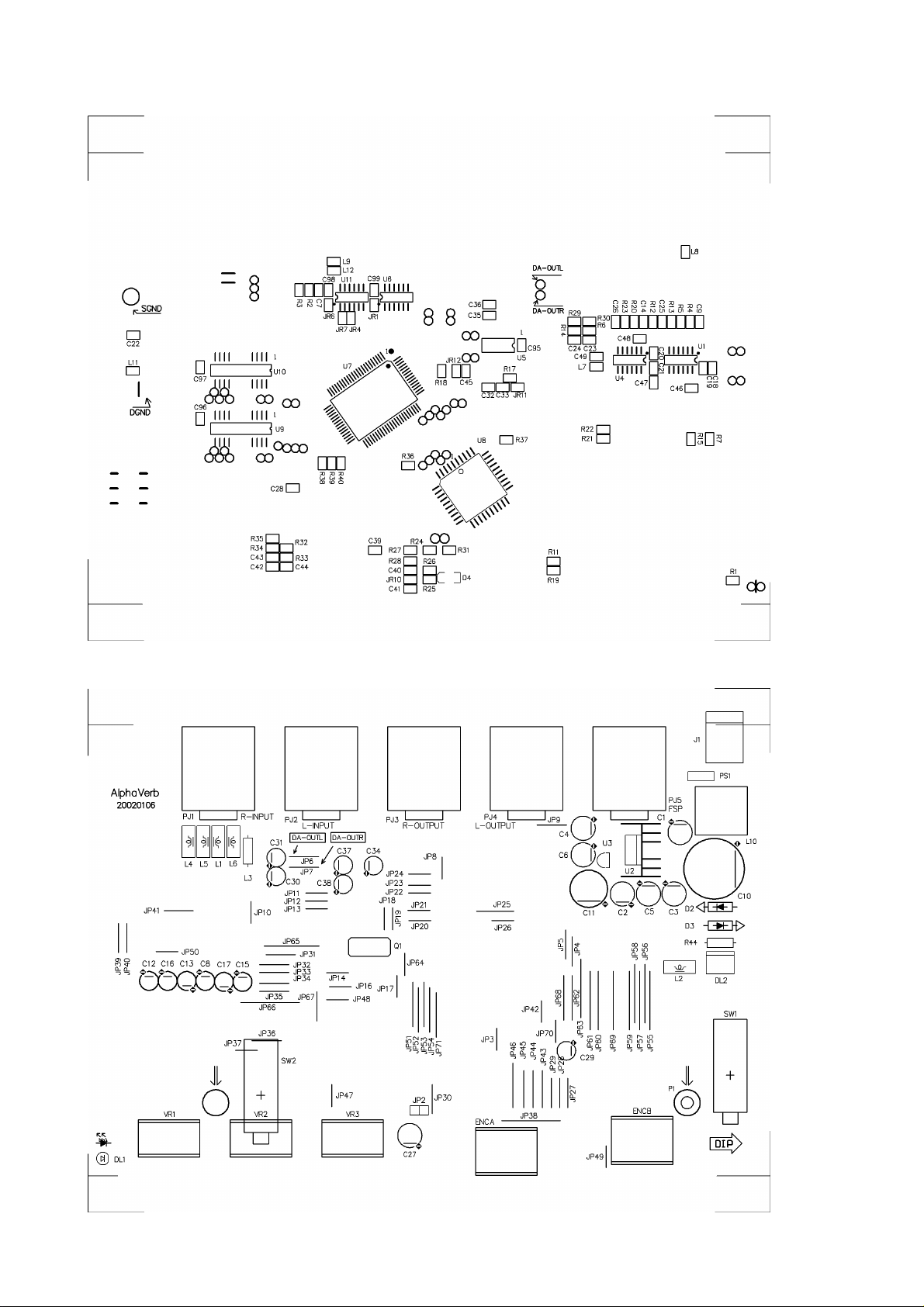
4. Print Circuit Board
BOTTOM SOLDER MASK
Page 8
BOTTOM SILKSCREEN
TOP SILKSCREEN
Page 9
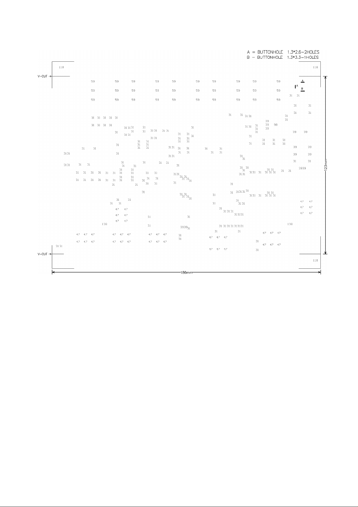
DRILL DRAWING
Tool Hole Size Hole Count Plated
--------------------------------------------------------------------------T1 31mil (0.80mm) 203
T2 39mil (1.00mm) 13
T3 47mil (1.20mm) 42
T4 59mil (1.50mm) 30
T5 98mil (2.50mm) 1
T6 118mil (3.00mm) 3
T7 138mil (3.50mm) 2
--------------------------------------------------------------------------Totals 294
Page 10
Page 11

Page 12

G1 Test Procedures (aCOMP)
Required Equipment
Audio Precision System 2 with APWin software
100 Mhz oscilloscope connected to APS2 Analyzer Signal Monitor outputs (Ch. A and Ch. B)
Connection Mode
Use Audio Precision System 2 analog unbalanced (BNC) inputs/outputs.
Page 13
Test Procedures for AlphaComp
Amplitude response test
On PC:
-Load file: alfacomp_amplitude (APWin File menu / Open / Test )
Test Connections:
-Output A of Audio Precision System Two --> LEFT input of the device under test.
-LEFT output of the device under test --> A input of Audio Precision System Two
-RIGHT output of the device under test --> B input of Audio Precision System Two
On the Alphacomp:
-Turn on the power switch.
-Set INPUT volume to maximum.
-Set OUTPUT volume to maximum.
-Set PROGRAM to AGC PURE.
-Set VARIATION to 1.
Start the sweep (F9) and control the results (Page3 – Graph) in the following conditions:
-hardware bypass switch pressed.
-hardware bypass switch released.
Audio Precision 05/22/02 14:07:53
+10
+7.5
+5
+2.5
d
+0
B
V
-2.5
-5
-7.5
-10
20 20k50 100 200 500 1k 2k 5k 10k
Hz
Color Line Style Thick Data Axis
Cyan Solid 1 Anlr.Level A Left
Gree n Solid 1 Anlr.Level B Right
Yellow Solid 1 Anl r .Am p l Left
+10
+7.5
+5
+2.5
+0
-2.5
-5
-7.5
-10
d
B
V
alfacomp_amplitude.at2c
Page 14

THD test
On PC:
-Load file: alfacomp_THD (APWin File menu / Open / Test )
Test Connections:
-Output A of Audio Precision System Two --> LEFT input of the device under test.
On the Alphacomp:
-Turn on the power switch.
-Set INPUT volume to maximum.
-Set OUTPUT volume to maximum.
-Set PROGRAM to AGC PURE.
-Set VARIATION to 1.
Start the sweep (F9) and control the results (Page3 – Graph) in the following conditions:
-LEFT output of the device under test --> A input of Audio Precision System Two / hardware
bypass switch released.
-RIGHT output of the device under test --> B input of Audio Precision System Two /
hardware bypass switch released.
Audio Precision 05/22/02 14:10:23
1
0.9
0.8
0.7
0.6
0.5
%
0.4
0.3
0.2
0.1
20 6k50 100 200 500 1k 2k
Hz
Color Line Style Th ick Data Axi s
Cyan Solid 1 Anlr.THD+N Ratio Left
Gree n Solid 1 Anlr.THD+N Ratio Left
alfacomp_THD.at2c
Page 15

S/N test
On PC:
-Load file: alfacomp_SN (APWin File menu / Open / Test )
Test Connections:
-Output A of Audio Precision System Two --> LEFT input of the device under test.
On the Alphacomp:
-Turn on the power switch.
- With hardware bypass switch in COMP position and both outputs connected to the Audio
Precision, increase the INPUT level until the device`s outputs clip, and after reduce the INPUT
level itself until the outputs exit from clipping state.
-Set OUTPUT volume to maximum.
-Set PROGRAM to AGC PURE.
-Set VARIATION to 1.
Start the sweep (F9) and control the results (Page3 – Graph) in the following conditions:
-LEFT output of the device under test --> A input of Audio Precision System Two / hardware
bypass switch pressed.
-RIGHT output of the device under test --> B input of Audio Precision System Two /
hardware bypass switch pressed.
Audio Precision 05/22/02 14:13:55
+20
+0
-20
-40
d
B
V
-60
-80
-100
-120
-1000.000 +0-900 -800 -700 -600 -500 -400 -300 -2 00 -10 0
PROCESSBYPASS
dBV
Color Line Style Th ick Data Axi s
Cyan Solid 1 An lr .Am p l Left
Gree n Solid 1 An l r. Am pl Left
alfacomp_SN.at2c
Page 16

Dynamics test
On PC:
-Load file: alfacomp_dyn (APWin File menu / Open / Test )
Test Connections:
-Output A of Audio Precision System Two --> LEFT input of the device under test.
On the Alphacomp:
-Turn on the power switch.
-Set INPUT volume to maximum.
-Set OUTPUT volume to maximum.
-Set PROGRAM to AGC PURE.
-Set VARIATION to 1.
Start the sweep (F9) and control the results (Page3 – Graph) in the following conditions:
-LEFT output of the device under test --> A input of Audio Precision System Two / hardware
bypass switch pressed.
-RIGHT output of the device under test --> B input of Audio Precision System Two /
hardware bypass switch pressed.
Audio Precision 05/22/02 14:17:59
16
14
12
10
%
8
6
4
2
-0
Color Line Style Thi ck Data Axi s
Cyan Solid 1 Anlr.THD+N Ratio Left
Gree n Solid 1 Anlr.Level A Right
Gree n Solid 1 Anlr.THD+N Ratio Left
Yellow Solid 1 Anlr.Level A Right
-26 -14-24 -22 -20 -18 -16
PROCESS
dBu
BYPASS
BYPASS
+10
+7.5
+5
+2.5
+0
-2.5
-5
-7.5
B
d
u
alfacom p_ dyn.a t2c
Page 17

Stability test
On PC:
-Load file: alfacomp_stability (APWin File menu / Open / Test )
Test Connections:
-Output A of Audio Precision System Two --> LEFT input of the device under test.
-LEFT output of the device under test --> A input of Audio Precision System Two
-RIGHT output of the device under test --> B input of Audio Precision System Two
On the Alphacomp:
-Turn on the power switch.
-Set OUTPUT volume to maximum.
-Set PROGRAM to AGC PURE.
-Set hardware bypass switch to BYPASS (released).
-Set VARIATION to 1.
Test:
Move the input level knob from 0 to maximum 3 times and control the output waveforms:
NO PERMANENT SINE WAVEFORMS should be visible. IF PERMANENT
WAVEFORMS WITH FREQUENCY > 20 kHz should become visible on whatever output
channel, THE UNIT IS TO BE INSPECTED.
Page 18

SEKAKU ELECTRON INDUSTRY CO.,LTD
O
e
IEBO_P02 IEBO_P02
Multi-Level BOM Structure Listing
Report No.: IEBO_P02 Date 2003/08/20
Prepared by 000011[YAFEN] Page No.: 1/9
Item No. PF00076 Version UNIT: PCS
DESCRIPTI
aCOMP Date: 2002/04/16
aCOMP_ALTO_230V_歐規_無
Version Item No Loss % Ver. Unit Cardinal Effective Date
Item Description Usage Rat
@:Phantom Layer
Component Remark Attrition Rate
├0001---------------------------------
││
││
├0002---------------------------------
││
││
├0003---------------------------------
││
││
├0004---------------------------------
││
││
├0005---------------------------------
│
│
├0006---------------------------------
│
│
├0007---------------------------------
│
│
├0008---------------------------------
│
│
├0009---------------------------------
│
│
├0010---------------------------------
│
│
├0011---------------------------------
│
│
├0012---------------------------------
│
│
├0013---------------------------------
│
│
├0014---------------------------------
│
│
├0015---------------------------------
│
│
MA02918 1.0000 2002/04/16
panel(white) PCS 1 N
αComp ▲LTO
0.00 %
MB01615 1.0000 2002/04/16
bottom board PCS 1 N
a verb 0.00 %
MC00371 1.0000 2002/04/16
top cover PCS 1 N
aVERB 0.00 %
MB01957 1.0000 2002/04/16
rear board PCS 1 N
a verb 0.00 %
NI00363 1.0000 2002/04/16
plastic knob PCS 1 N
φ21*16
0.00 %
NI00362 3.0000 2002/04/16
plastic knob PCS 1 N
(COOL GRAY 8C/white) 0.00 %
NI00896 3.0000 2002/04/16
knob cover-ABS PCS 1 N
φ8.5*4 bule 072C
0.00 %
NI00307 1.0000 2002/04/16
power sw bottom PCS 1 N
φ15*12
0.00 %
NI01160 1.0000 2002/04/16
power switch cap PCS 1 N
φ14.5*10 YELLOW C
0.00 %
NI00314 1.0000 2002/04/16
power sw bottom PCS 1 N
φ6.5*16(inner 3.3*3.3)black
0.00 %
MG00025 10.0000 2002/04/16
screw PCS 1 N
M3*6 0.00 %
MG00163 2.0000 2002/04/16
Ni-screw PCS 1 N
M3*8 0.00 %
MG00045 4.0000 2002/04/16
screw PCS 1 N
M3*7 0.00 %
NI00002 5.0000 2002/04/16
nut of plastic-HC00108 Appendix PCS 1 N
φ7/16"*G20/15*4.8(hexagon)
0.00 %
MF00014 2.0000 2002/04/16
outter gear washer PCS 1 N
φ3*φ6.5*0.5t
0.00 %
Page 19

SEKAKU ELECTRON INDUSTRY CO.,LTD
O
e
IEBO_P02 IEBO_P02
Multi-Level BOM Structure Listing
Report No.: IEBO_P02 Date 2003/08/20
Prepared by 000011[YAFEN] Page No.: 2/9
Item No. PF00076 Version UNIT: PCS
DESCRIPTI
aCOMP Date: 2002/04/16
aCOMP_ALTO_230V_歐規_無
Version Item No Loss % Ver. Unit Cardinal Effective Date
Item Description Usage Rat
@:Phantom Layer
Component Remark Attrition Rate
├0016---------------------------------
│
│
├0017---------------------------------
│
│
├0018---------------------------------
│
│
├0019---------------------------------
││
││
├0020---------------------------------
│
│
├0021---------------------------------
││
││
├0022---------------------------------
│
│
├0023---------------------------------
│
│
├0024---------------------------------
│
│
├0025---------------------------------
││
││
├0026---------------------------------
│
│
├0027---------------------------------
│
│
├0028---------------------------------
│
│
├0029---------------------------------
││
││
├0030---------------------------------
│
│
HA01388 1.0000 2002/04/16
row-wire connector wiring PCS 1 N
2P 100 0.00 %
NC00131 5.0000 2002/05/05
washer PCS 1 N
1*φ11.3*φ15.3 red
0.00 %
SA00065 1.0000 2002/05/05
L.E.D PCS 1 N
LG2043 green 0.00 %
NI00240 2.0000 2002/05/05
sleeving flame retardant PCS 1 N
φ2.5*10mm
0.00 %
TG00023 1.0000 2002/05/05
voltage transformer PCS 1 N
230V/50Hz_AC9V/300mA_ET-35_CE 0.00 %
NF00124 1.0000 2002/05/05
instruction PCS 1 N
aCOMP 0.00 %
HJ00002 1.0000 2002/05/05
desiccant PCS 1 N
10g 0.00 %
NA00122 1.0000 2002/05/05
PE bag PCS 1 N
0.04t*350*230mm KG 0.00 %
NA00137 1.0000 2002/05/05
clip-chain bag PCS 1 N
5*7 0.00 %
NI01825 1.0000 2002/05/05
ZD-cushion-aVERB-10 PCS 1 N
0.5*φ3.3*φ8.3 aVERB
0.00 %
NA00146 1.0000 2002/05/05
bubble bag PCS 1 N
13*16 0.00 %
NI00501 4.0000 2002/05/05
foot cushion PCS 1 N
12.7*9*3t(SF-004) 0.00 %
NI02085 1.0000 2002/07/19
power switch fixed sleeve PCS 1 N
φ22*9.69 072C blue
0.00 %
NE03118 1.0000 2002/07/19
program adhesive paper 12*9mm PCS 1 N
aCOMP CKS:C47F 0.00 %
NB01480 1.0000 2002/07/19
colour box PCS 1 N
aCOMP ALTO 0.00 %
Page 20

SEKAKU ELECTRON INDUSTRY CO.,LTD
O
e
m
m
IEBO_P02 IEBO_P02
Multi-Level BOM Structure Listing
Report No.: IEBO_P02 Date 2003/08/20
Prepared by 000011[YAFEN] Page No.: 3/9
Item No. PF00076 Version UNIT: PCS
DESCRIPTI
aCOMP Date: 2002/04/16
aCOMP_ALTO_230V_歐規_無
Version Item No Loss % Ver. Unit Cardinal Effective Date
Item Description Usage Rat
@:Phantom Layer
Component Remark Attrition Rate
├0031---------------------------------
│
│
├0032---------------------------------
││
││
├0033---------------------------------
││
││
├0034---------------------------------
│
│
├0035---------------------------------
││
││
│├0001-------------------------------
││
││
NB02141 1.0000 2002/12/05
outter carton 8 hole PCS 8 N
aVERB aCOMP aMICTUBE ALTO 0.00 %
MI00408 1.0000 2002/07/19
conduct electricity board PCS 1 N
aVERB 0.00 %
NE05008 4.0000 2002/07/19
ZC-bar shape code abhesive paper 30*11
PCS 1 N
ACOMP 0.00 %
NE05004 4.0000 2002/07/19
number bar shape adhevise paper 30*11m
PCS 1 N
ALTO PF 0.00 %
HK00337 1.0000 2002/07/19
PC board PCS 1 N
P-aCOMP-DIP 0.00 %
RA00204 1.0000 2002/04/16
fixed resistor 1/4W PCS 1 N
470Ω M type
0.00 %
R44
│├0002-------------------------------
││
││
CB00009 3.0000 2002/04/16
electrolytic capacitor PCS 1 N
1uF/50V ψ4*7mm
0.00 %
C29 C30 C31
│├0003-------------------------------
││
││
CB00024 5.0000 2002/04/16
electrotytic capacitor PCS 1 N
10uF/16V ψ4*7mm
0.00 %
R34 R37 R38 R5 R6
│├0004-------------------------------
││
││
CB00040 6.0000 2002/04/16
electrotytic capacitor PCS 1 N
47uF/25V φ5*11mm
0.00 %
C12 C13 C15 C16 C17 C8
│├0005-------------------------------
││
││
CB00039 1.0000 2002/04/16
electrotytic capacitor PCS 1 N
47uF/25V φ5*11mm
0.00 %
C27
│├0006-------------------------------
││
││
CB00047 4.0000 2002/04/16
electrotytic capacitor PCS 1 N
100uF/25V φ6*11mm
0.00 %
C1 C2 C3 C4
│├0007-------------------------------
││
││
CB00056 1.0000 2002/04/16
electrolytic capacitor PCS 1 N
220uF/25V φ8*11mm
0.00 %
C11
│├0008-------------------------------
││
││
CB00080 1.0000 2002/04/16
electrotytic capacitor PCS 1 N
2200uF/25V φ16*25mm
0.00 %
Page 21

SEKAKU ELECTRON INDUSTRY CO.,LTD
O
e
IEBO_P02 IEBO_P02
Multi-Level BOM Structure Listing
Report No.: IEBO_P02 Date 2003/08/20
Prepared by 000011[YAFEN] Page No.: 4/9
Item No. PF00076 Version UNIT: PCS
DESCRIPTI
aCOMP Date: 2002/04/16
aCOMP_ALTO_230V_歐規_無
Version Item No Loss % Ver. Unit Cardinal Effective Date
Item Description Usage Rat
@:Phantom Layer
Component Remark Attrition Rate
C10
│├0009-------------------------------
││
││
SA00094 2.0000 2002/04/16
rectifier diode PCS 1 N
1N4002/100V 0.00 %
D2 D3
│├0010-------------------------------
││
││
SD00074 1.0000 2002/04/16
integrated circuit PCS 1 N
7805(TO-220) 0.00 %
U2
│├0011-------------------------------
││
││
SB00083 1.0000 2002/04/16
voltage stabilized transistor PCS 1 N
79L05(TO-92) 0.00 %
U3
│├0012-------------------------------
││
││
SC00002 1.0000 2002/04/16
quartz crystalloid PCS 1 N
11.0592MHZ HC-49/US ±20PPM 0.00 %
Q1
│├0013-------------------------------
││
││
CN00026 1.0000 2002/04/16
indutor PCS 1 N
330uH(LGA0307-331K) 0.00 %
L3
│├0014-------------------------------
││
││
CG00018 5.0000 2002/04/16
filter-EMI FILTER PCS 1 N
LF-22UH(WAH TAYI) 0.00 %
L1 L2 L4 L5 L6
│├0015-------------------------------
││
││
│├0016-------------------------------
││
││
HI00073 2.0000 2002/04/16
waveband switch PCS 1 N
288S0121 0.00 %
HI00047 1.0000 2002/04/16
button SW(double link-action)) PCS 1 N
PS-9AN-022-18B long foot 0.00 %
SW1
│├0017-------------------------------
││
││
HI00051 1.0000 2002/04/16
key swith (double-link) PCS 1 N
PS-9AN-022-18A 0.00 %
SW2
│├0018-------------------------------
││
││
RC00086 2.0000 2002/04/16
potentiometer PCS 1 N
A10KΩ*2 RV16A01-20-20F-A14-301
0.00 %
VR1 VR3
│├0019-------------------------------
││
││
HC00108 5.0000 2002/04/16
MIC jack PCS 1 N
φ6.3 stereo LJB0661-6
0.00 %
PJ1 PJ2 PJ3 PJ4 PJ5
│├0020-------------------------------
││
HC00183 1.0000 2002/04/16
DC jack PCS 1 N
Page 22

SEKAKU ELECTRON INDUSTRY CO.,LTD
O
e
IEBO_P02 IEBO_P02
Multi-Level BOM Structure Listing
Report No.: IEBO_P02 Date 2003/08/20
Prepared by 000011[YAFEN] Page No.: 5/9
Item No. PF00076 Version UNIT: PCS
DESCRIPTI
aCOMP Date: 2002/04/16
aCOMP_ALTO_230V_歐規_無
Version Item No Loss % Ver. Unit Cardinal Effective Date
Item Description Usage Rat
@:Phantom Layer
Component Remark Attrition Rate
││
DJ-005A 0.00 %
J1
│├0021-------------------------------
││
││
SA00053 1.0000 2002/04/16
L.E.D high intensity PCS 1 N
3m/m round(red)long foot 26mm 0.00 %
DL1
│├0022-------------------------------
││
││
│├0023-------------------------------
││
││
NI01776 1.0000 2002/04/16
LED separating pillar PCS 1 N
LED-3 3mm 0.00 %
HC00076 1.0000 2002/04/16
row-wire header PCS 1 N
2P 2.5mm 180° 0.00 %
DL2
│├0024-------------------------------
││
││
HC00134 1.0000 2002/04/16
row-pin(single)#1100 PCS 1 N
2.54 180° 2P(gold-plated) 6/11.6mm 0.00 %
JP2
│├0025-------------------------------
││
││
CG00024 1.0000 2002/04/16
filter-EMI FITER PCS 1 N
PLT09H-2003R 0.00 %
L10
│├0026------------------------------││
││
│├0027------------------------------││
││
│├0028------------------------------││
││
│├0029------------------------------││
││
│├0030------------------------------│││
│││
│└0031------------------------------│ │
│ │
│ ├0001-----------------------------│ ││
│ ││
MI00256 1.0000 2002/04/16
heat-sink PCS 1 N
25*15*10.6-1PIN SCL-2020 0.00 %
MG00160 1.0000 2002/04/16
Ni-screw PCS 1 N
M3*6 P0.5 0.00 %
MF00037 1.0000 2002/04/16
spring washer PCS 1 N
φ3*φ5*1t
0.00 %
NC00005 1.0000 2002/04/16
silicone insulator PCS 1 N
TO-220 square type 0.00 %
NE03118 1.0000 2002/04/16
ZC-program adhesive paper 12*9mm PCS 1 N
aCOMP CKS:C47F 0.00 %
HK01577 1.0000 2003/07/29
PC board PCS 1
P-aCOMP-AI 0.00 %
HA01920 25.0000 2003/07/14
jumper wire PCS 1 N
6mm 0.00 %
JP10 JP11 JP12 JP13 JP14 JP16 JP17 JP18 JP19 JP20 JP21JP22 JP23 JP24
│ ││
│ ├0002-----------------------------│ ││
JP26 JP3 JP37 JP42 JP47 JP48 JP49 JP50 JP64 JP70 JP8
HA01922 19.0000 2003/07/14
jumper wire PCS 1 N
Page 23

SEKAKU ELECTRON INDUSTRY CO.,LTD
O
e
IEBO_P02 IEBO_P02
Multi-Level BOM Structure Listing
Report No.: IEBO_P02 Date 2003/08/20
Prepared by 000011[YAFEN] Page No.: 6/9
Item No. PF00076 Version UNIT: PCS
DESCRIPTI
aCOMP Date: 2002/04/16
aCOMP_ALTO_230V_歐規_無
Version Item No Loss % Ver. Unit Cardinal Effective Date
Item Description Usage Rat
@:Phantom Layer
Component Remark Attrition Rate
│ ││
8mm 0.00 %
JP27 JP28 JP29 JP30 JP31 JP32 JP33 JP34 JP35 JP36 JP39 JP4 JP40 JP41
│ ││
│ ├0003-----------------------------│ ││
│ ││
JP5 JP6 JP67 JP7 JP9
HA01925 4.0000 2003/07/14
jumper wire PCS 1 N
10mm 0.00 %
JP25 JP43 JP44 JP45
│ ├0004-----------------------------│ ││
│ ││
HA01928 8.0000 2003/07/14
jumper wire PCS 1 N
12mm 0.00 %
JP46 JP51 JP52 JP53 JP54 JP62 JP68 JP71
│ ├0005-----------------------------│ ││
│ ││
HA01930 1.0000 2003/07/14
jumper wire PCS 1 N
15mm 0.00 %
J65
│ ├0006-----------------------------│ ││
│ ││
HA01931 11.0000 2003/07/14
jumper wire PCS 1 N
16mm 0.00 %
JP38 JP55 JP56 JP57 JP58 JP59 JP60 JP61 JP63 JP66 JP69
│ └0007-----------------------------│ │
│ │
│ ├0001----------------------------│ │
│ │
│ ├0002----------------------------│ │
│ │ 0Ω ±5% 0805
│ │
│ ├0003----------------------------│ │
│ │ 100Ω ±5% 0805
HK00338 1.0000 2003/07/14
PC board PCS 1 Y
P-aCOMP-SMD 0.00 %
HB00007 1.0000 2002/04/16
PCB-CEM-1 PCS 1 N
ALPHAVERB_VER030517 0.00 %
RD00002 10.0000 2002/04/16
SMDfixed resistor 1/10W PCS 1 N
0.00 %
JR1 JR10 JR11 JR12 JR4 JR6 JR7 JR38 JR39 JR40
RD00006 2.0000 2002/04/16
SMDfixed resistor 1/10W PCS 1 N
0.00 %
R18 R31
│ ├0004----------------------------│ │
│ │ 220Ω ±5% 0805
RD00009 1.0000 2002/04/16
SMDfixed resistor 1/10W PCS 1 N
0.00 %
R1
│ ├0005----------------------------│ │
│ │ 270Ω ±5% 0805
RD00010 2.0000 2002/04/16
SMDfixed resistor 1/10W PCS 1 N
0.00 %
R20 R23
│ ├0006----------------------------│ │
│ │ 1.0KΩ ±5% 0805
RD00018 5.0000 2002/04/16
SMDfixed resistor 1/10W PCS 1 N
0.00 %
R12 R15 R3 R4 R7
│ ├0007-----------------------------
RD00023 2.0000 2002/04/16
Page 24

SEKAKU ELECTRON INDUSTRY CO.,LTD
O
e
IEBO_P02 IEBO_P02
Multi-Level BOM Structure Listing
Report No.: IEBO_P02 Date 2003/08/20
Prepared by 000011[YAFEN] Page No.: 7/9
Item No. PF00076 Version UNIT: PCS
DESCRIPTI
aCOMP Date: 2002/04/16
aCOMP_ALTO_230V_歐規_無
Version Item No Loss % Ver. Unit Cardinal Effective Date
Item Description Usage Rat
@:Phantom Layer
Component Remark Attrition Rate
│ │
│ │ 2.2KΩ ±5% 0805
SMDfixed resistor 1/10W PCS 1 N
0.00 %
R14 R6
│ ├0008----------------------------│ │
│ │ 4.7KΩ ±5% 0805
RD00027 11.0000 2002/04/16
SMDfixed resistor 1/10W PCS 1 N
0.00 %
R11 R17 R19 R25 R26 R27 R28 R32 R33 R34 R35
│ ├0009----------------------------│ │
│ │ 10KΩ ±5% 0805
RD00032 5.0000 2002/04/16
SMDfixed resistor 1/10W PCS 1 N
0.00 %
R2 R21 R22 R36 R37
│ ├0010----------------------------│ │
│ │ 100KΩ ±5% 0805
RD00049 3.0000 2002/04/16
SMDfixed resistor 1/10W PCS 1 N
0.00 %
R24 R29 R30
│ ├0011----------------------------│ │
│ │ 1.0MΩ ±5% 0805
RD00056 2.0000 2002/04/16
SMDfixed resistor 1/10W PCS 1 N
0.00 %
R13 R5
│ ├0012----------------------------│ │
│ │
CI00007 2.0000 2002/04/16
SMDceramic capacitor0805 PCS 1 N
22PF/50V NPO 0.00 %
C32 C33
│ ├0013----------------------------│ │
│ │
CI00012 4.0000 2002/04/16
SMDceramic capacitor0805 PCS 1 N
47PF/50V NPO 0.00 %
C46 C47 C48 C49
│ ├0014----------------------------│ │
│ │
CI00015 1.0000 2002/04/16
SMD ceramic capacitor0805 PCS 1 N
82PF/50V NPO 0.00 %
C45
│ ├0015----------------------------│ │
│ │
CI00018 2.0000 2002/04/16
SMDceramic capacitor0805 PCS 1 N
220PF/50V NPO ±5% 0.00 %
C25 C9
│ ├0016----------------------------│ │
│ │
CI00019 2.0000 2002/04/16
SMDceramic capacitor0805 PCS 1 N
470PF/50V NPO ±5% 0.00 %
C35 C36
│ ├0017----------------------------│ │
│ │
CI00020 2.0000 2002/04/16
SMDceramic capacitor0805 PCS 1 N
680PF/50V NPO 0.00 %
C23 C24
│ ├0018----------------------------│ │
│ │
CI00028 2.0000 2002/04/16
SMDceramic capacitor0805 PCS 1 N
0.01uF/50V Y5V 0.00 %
Page 25

SEKAKU ELECTRON INDUSTRY CO.,LTD
O
e
IEBO_P02 IEBO_P02
Multi-Level BOM Structure Listing
Report No.: IEBO_P02 Date 2003/08/20
Prepared by 000011[YAFEN] Page No.: 8/9
Item No. PF00076 Version UNIT: PCS
DESCRIPTI
aCOMP Date: 2002/04/16
aCOMP_ALTO_230V_歐規_無
Version Item No Loss % Ver. Unit Cardinal Effective Date
Item Description Usage Rat
@:Phantom Layer
Component Remark Attrition Rate
C14 C26
│ ├0019----------------------------│ │
│ │
CI00029 18.0000 2002/04/16
SMDceramic capacitor0805 PCS 1 N
0.1uF/50V Y5V 0.00 %
C18 C19 C20 C21 C22 C28 C39 C40 C41 C42 C43 C44 C7 C95 C96 C97
│ │
│ ├0020----------------------------│ │
│ │
C98 C99
SE00011 1.0000 2002/04/16
SMD rectifier diode PCS 1 N
RLS4148 0.5A (LL-34) 0.00 %
D4
│ ├0021----------------------------│ │
│ │
SG00067 1.0000 2002/04/16
SMD integraded circuit PCS 1 N
74HC04DT 0.00 %
U11
│ ├0022----------------------------│ │
│ │
SG00070 1.0000 2002/04/16
SMD integratd circuit PCS 1 N
74HC393DT 0.00 %
U6
│ ├0023----------------------------│ │
│ │
SG00001 2.0000 2002/04/16
SMD integrated circuit PCS 1 N
TL074CDT 0.00 %
U1 U4
│ ├0024----------------------------│ │
│ │
SG00036 1.0000 2002/04/16
SMD integratd circuit PCS 1 N
PCM3001E 0.00 %
U5
│ ├0025----------------------------│ │
│ │
SG00088 1.0000 2002/04/16
SMD integratd circuit PCS 1 N
P87C52SBAA(UBAA) 0.00 %
U8
│ ├0026----------------------------│ │
│ │
SG00114 1.0000 2002/04/16
smd integrated circut PCS 1 N
TMS57002DPHA 0.00 %
U7
│ ├0027----------------------------│ │
│ │
SG00115 2.0000 2002/04/16
smd integrated circut PCS 1 N
MB81C4256A-60PJ 0.00 %
U10 U9
│ └0028-----------------------------
│
│
CO00006 5.0000 2002/04/16
SMD inductor PCS 1 N
BLM21A102SPT 0.00 %
L11 L12 L7 L8 L9
├0036---------------------------------
││
││
├0037---------------------------------
NE05249 1.0000 2002/12/24
ZC- program adhesive paper 30*11mm PCS 1
aCOMP 0.00 %
NI02408 3.0000 2003/03/05
Page 26

SEKAKU ELECTRON INDUSTRY CO.,LTD
O
e
IEBO_P02 IEBO_P02
Multi-Level BOM Structure Listing
Report No.: IEBO_P02 Date 2003/08/20
Prepared by 000011[YAFEN] Page No.: 9/9
Item No. PF00076 Version UNIT: PCS
DESCRIPTI
Version Item No Loss % Ver. Unit Cardinal Effective Date
Component Remark Attrition Rate
│
│
├0038---------------------------------
│
│
└0039---------------------------------
aCOMP Date: 2002/04/16
aCOMP_ALTO_230V_歐規_無
Item Description Usage Rat
fixed piece-ABS PCS 1
φ15*2.7mm white CONTROL30
NI02409 1.0000 2003/03/05
fixed piece-ABS PCS 1
φ25*2.5mm aVERB
NF00061 1.0000 2003/05/15
assurance card PCS 1
ALTO 0.00 %
@:Phantom Layer
0.00 %
0.00 %
Page 27

8. Exploded Views
 Loading...