

Page 1

V-Series Avalon-MM DMA Interface for PCIe Solutions
User Guide
Last updated for Altera Complete Design Suite: 14.1
Subscribe
Send Feedback
UG-01154
2014.12.18
101 Innovation Drive
San Jose, CA 95134
www.altera.com
Page 2
2014.12.18
Bridge
and DMA
Engine
PCIe Hard IP
Block
PIPE
Interface
PHY IP Core
for PCIe
(PCS/PMA)
Serial Data
Transmission
Application
Layer
(User Logic)
Avalon-MM with
DMA Interface
www.altera.com
101 Innovation Drive, San Jose, CA 95134
Datasheet
1
UG-01154
Subscribe
Send Feedback
V-Series Avalon-MM DMA Interface for PCIe Datasheet
Altera® V-Series FPGAs include a configurable, hardened protocol stack for PCI Express
compliant with PCI Express Base Specification 2.1 or 3.0.
The V-Series Avalon ® Memory-Mapped (Avalon-MM) DMA for PCI Express removes some of the
complexities associated with the PCIe protocol. For example, the IP core handles TLP encoding and
decoding. In addition, it includes Read DMA and Write DMA engines. If you have already architected
your own DMA system with the Avalon-MM interface, you may want to continue to use it. However, you
will probably benefit from the simplicity of having the DMA engines already implemented. Altera
recommends this variant for new users. Depending of the device you select, this variant is available in
Qsys for 128- and 256-bit interfaces to the Application Layer. The Avalon-MM interface and DMA
engines are implemented in FPGA soft logic.
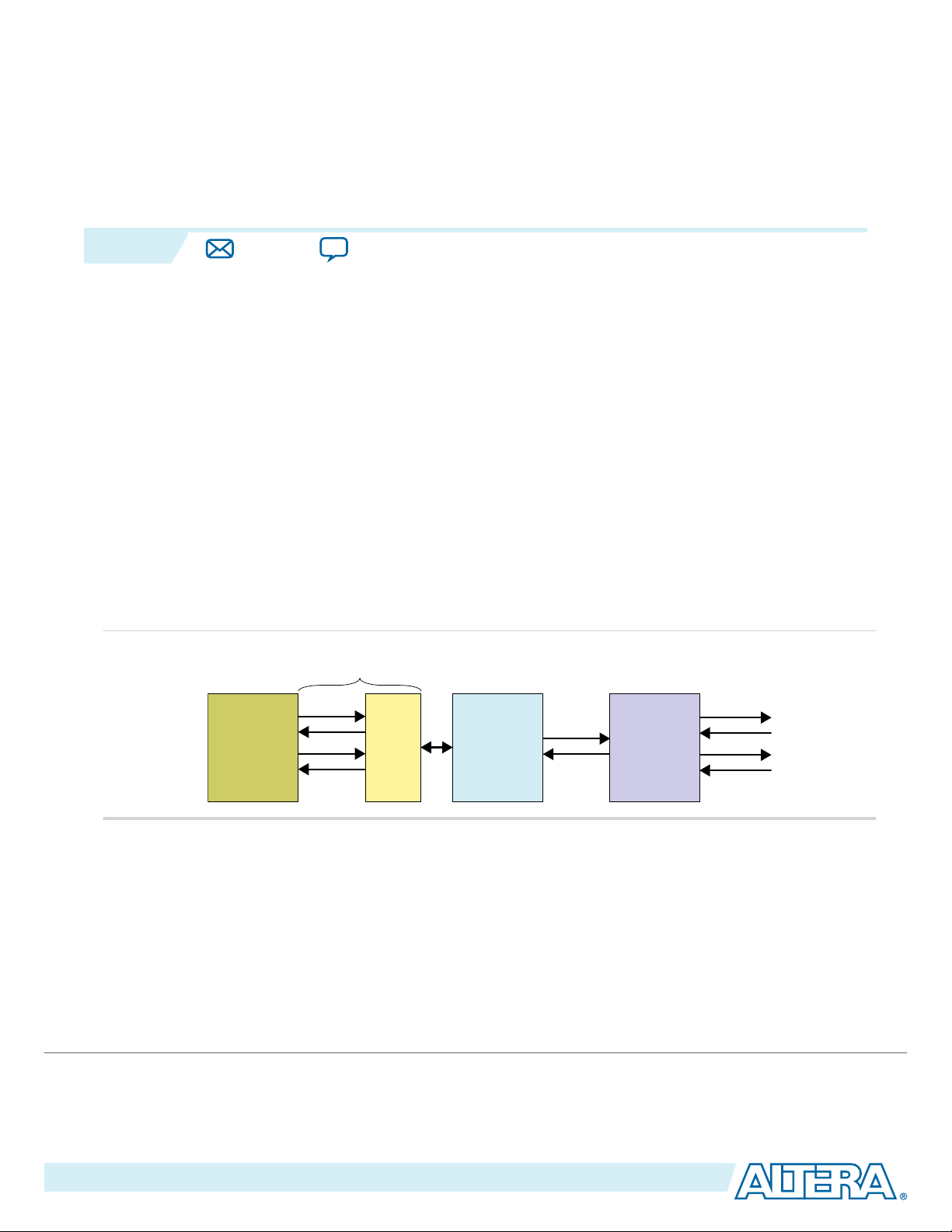
Figure 1-1: V-Series PCIe Variant with Avalon-MM DMA Interface
The following figure shows the high-level modules and connecting interfaces for this variant.
®
that is
Note:
©
2014 Altera Corporation. All rights reserved. ALTERA, ARRIA, CYCLONE, ENPIRION, MAX, MEGACORE, NIOS, QUARTUS and STRATIX words and logos are
trademarks of Altera Corporation and registered in the U.S. Patent and Trademark Office and in other countries. All other words and logos identified as
trademarks or service marks are the property of their respective holders as described at www.altera.com/common/legal.html. Altera warrants performance
of its semiconductor products to current specifications in accordance with Altera's standard warranty, but reserves the right to make changes to any
products and services at any time without notice. Altera assumes no responsibility or liability arising out of the application or use of any information,
product, or service described herein except as expressly agreed to in writing by Altera. Altera customers are advised to obtain the latest version of device
specifications before relying on any published information and before placing orders for products or services.
This variant was renamed in the Quartus® II 14.0 release. The name in the Quartus II 13.1 release
was Avalon-MM 256-bit Hard IP for PCI Express IP Core.
ISO
9001:2008
Registered
Page 3

1-2
Features
UG-01154
2014.12.18
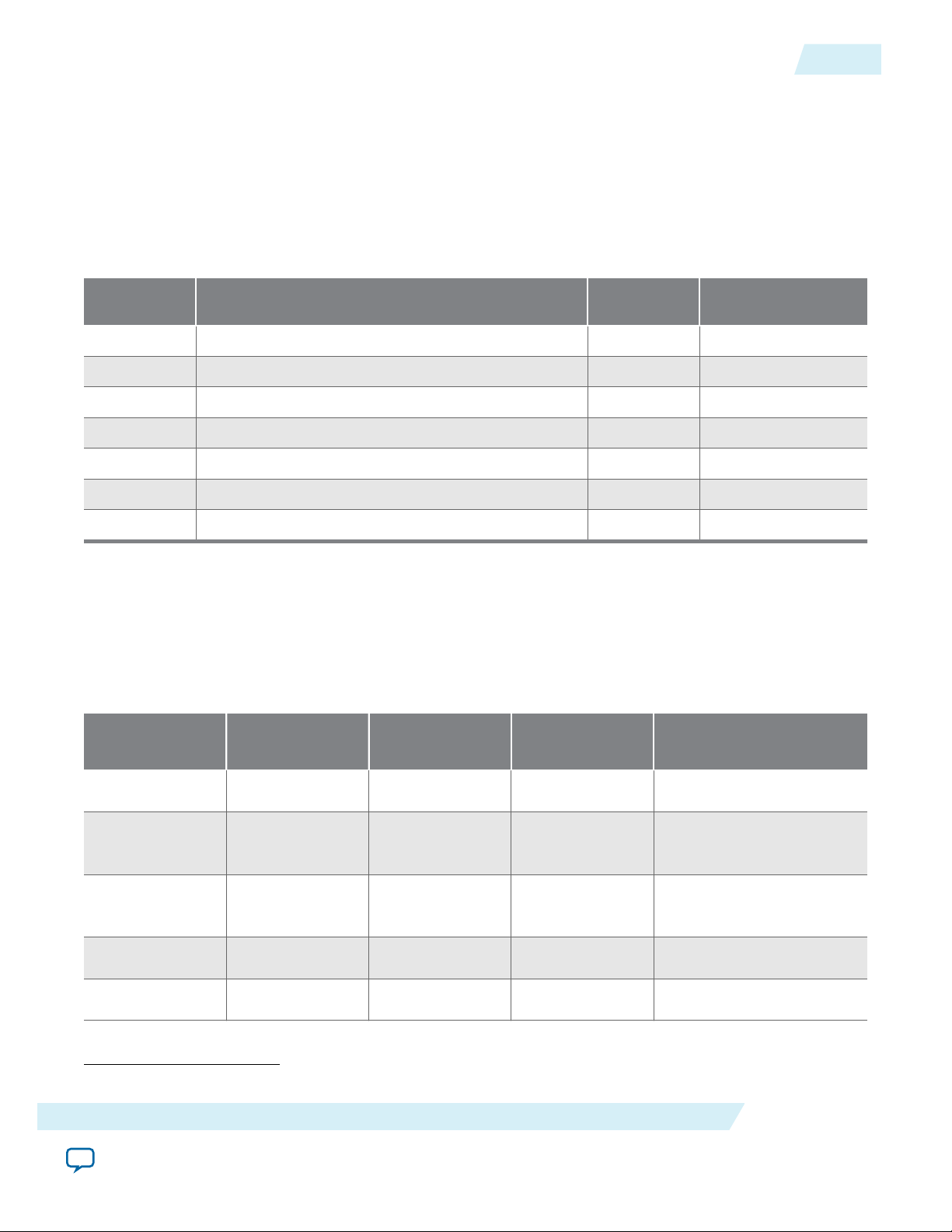
Table 1-1: PCI Express Data Throughput
The following table shows the aggregate bandwidth of a PCI Express link for Gen1, Gen2, and Gen3 for 2, 4, and 8
lanes. The protocol specifies 2.5 giga-transfers per second for Gen1, 5.0 giga-transfers per second for Gen2, and
8.0 giga-transfers per second for Gen3. This table provides bandwidths for a single transmit (TX) or receive (RX)
channel. The numbers double for duplex operation. Gen1 and Gen2 use 8B/10B encoding which introduces a 20%
overhead. In contrast, Gen3 uses 128b/130b encoding which reduces the data throughput lost to encoding to less
than 1%.
Link Width in Gigabits Per Second (Gbps)
×2 ×4 ×8
PCI Express Gen1 (2.5 Gbps)
N/A N/A
PCI Express Gen2 (5.0 Gbps) 8 16 32
PCI Express Gen3 (8.0 Gbps) 15.75 31.51 63
Related Information
• PCI Express Base Specification 2.1 or 3.0
• PCI Express DMA Reference Design for Stratix V Devices
• Creating a System with Qsys
Features
New features in the Quartus® II 14.1 software release:
• New PCI Express Multi-Channel DMA Interface IP Core to demonstrate multi-channel operation.
This component is available in the Qsys IP Catalog under Interface Protocols > PCI Express > Qsys
Example Designs
• New Avalon-MM DMA FIFO Mode IP Core for PCI Express to provide a FIFO interface to the Data
Mover included in the Avalon-MM bridge. This component is available in the Qsys IP Catalog under
Interface Protocols > PCI Express > Qsys Example Designs
• Support for 128-Bit Avalon-MM RX master.
• Reduced Quartus II compilation warnings by 50%.
16
The V-Series Avalon-MM DMA for PCI Express supports the following features:
• Complete protocol stack including the Transaction, Data Link, and Physical Layers implemented as
• Native support for Gen1 x8, Gen2 x4, Gen2 x8, Gen3 x4, Gen3 x8 for Endpoints. The variant
• Dedicated 16 KByte receive buffer.
• Optional hard reset controller for Gen2.
• Support for 128- or 256-bit Avalon-MM interface to Application Layer with embedded DMA up to
• Support for 32- or 64-bit addressing for the Avalon-MM interface to the Application Layer.
• Qsys example designs demonstrating parameterization, design modules, and connectivity.
Altera Corporation
hard IP.
downtrains when plugged into a lesser link width or changes to a different maximum link rate.
Gen3 ×8 data rate.
Datasheet
Send Feedback
Page 4
UG-01154
2014.12.18
Features
• Extended credit allocation settings to better optimize the RX buffer space based on application type.
• Optional end-to-end cyclic redundancy code (ECRC) generation and checking and advanced error
reporting (AER) for high reliability applications.
• Support for Configuration Space Bypass Mode, allowing you to design a custom Configuration Space
and support multiple functions.
• Support for Gen3 PIPE simulation.
• Support for V-Series Avalon-MM DMA for PCI Express with either a 128- or 256-bit interface to the
Application Layer. This variant includes an embedded DMA controller for data transfers. The
following table shows the available configurations.
Configuration Available Devices Interface
Width
Application Layer
Clock Frequency
Gen1 x8 Arria® V, Arria V GZ, Stratix® V 128 bits 125 MHz
Gen2 x4 Arria V, Arria V GZ, Cyclone, ® V Stratix V 128 bits 125 MHz
Gen2 x8 Arria V GZ, Stratix V 128 bits 250 MHz
Gen2 x8 Arria V GZ, Stratix V 256 bits 125 MHz
Gen3 x4 Arria V GZ, Stratix V 128 bits 250 MHz
Gen3 x4 Arria V GZ, Stratix V 256 bits 125 MHz
1-3
Gen3 x8 Arria V GZ, Stratix V 256 bits 250 MHz
• Easy to use:
• Flexible configuration.
• No license requirement.
• Example designs to get started.
Table 1-2: Feature Comparison for all Hard IP for PCI Express IP Cores
The table compares the features of the four Hard IP for PCI Express IP Cores.
Feature Avalon‑ST Interface Avalon‑MM
Interface
Avalon‑MM DMA Avalon‑ST Interface with SR-
IOV
IP Core License Free Free Free Free
Native
Supported Supported Supported Supported
Endpoint
Legacy
Endpoint
(1)
Supported Not Supported Not Supported Not Supported
Root port Supported Supported Not Supported Not Supported
(1)
Datasheet
Gen1 ×1, ×2, ×4, ×8 ×1, ×2, ×4, ×8 Not Supported
Not recommended for new designs.
Send Feedback
×8
Altera Corporation
Page 5

1-4
Features
UG-01154
2014.12.18
Feature Avalon‑ST Interface Avalon‑MM
Interface
Avalon‑MM DMA Avalon‑ST Interface with SR-
Gen2 ×1, ×2, ×4, ×8 ×1, ×2, ×4, ×8 ×4, ×8
Gen3 ×1, ×2, ×4, ×8 ×1, ×2, ×4 ×4, ×8
64-bit Applica‐
Supported Supported Not supported Not supported
tion Layer
interface
128-bit
Supported Supported Supported Supported
Application
Layer interface
256-bit
Supported Not Supported Supported Supported
Application
Layer interface
IOV
×4, ×8
×2, ×4, ×8
Altera Corporation
Datasheet
Send Feedback
Page 6

UG-01154
2014.12.18
Features
1-5
Feature Avalon‑ST Interface Avalon‑MM
Interface
Transaction
Layer Packet
type (TLP)
• Memory Read
Request
• Memory Read
RequestLocked
• Memory Write
Request
• I/O Read
Request
• I/O Write
Request
• Configuration
Read Request
(Root Port)
• Configuration
Write Request
(Root Port)
• Message
Request
• Message
Request with
Data Payload
• Completion
Message
• Completion
with Data
• Memory Read
Request
• Memory Write
Request
• I/O Read
Request—Root
Port only
• I/O Write
Request—Root
Port only
• Configuration
Read Request
(Root Port)
• Configuration
Write Request
(Root Port)
• Completion
Message
• Completion
with Data
• Memory Read
Request (single
dword)
• Memory Write
Request (single
dword)
• Completion for
Locked Read
without Data
Avalon‑MM DMA Avalon‑ST Interface with SR-
IOV
• Memory Read
Request
• Memory Write
Request
• Completion
Message
• Completion
with Data
• Memory Read Request
• Memory Write
Request
• Configuration Read
Request (from Root
Port)
• Configuration Write
Request (from Root
Port)
• Message Request
• Completion Message
• Completion with Data
Datasheet
Payload size
Number of tags
128–2048 bytes 128–256 bytes 128, 256, 512 bytes 128–256 bytes
256 8 16 256
supported for
non-posted
requests
62.5 MHz clock Supported Supported Not Supported Not Supported
Send Feedback
Altera Corporation
Page 7

1-6
Features
UG-01154
2014.12.18
Feature Avalon‑ST Interface Avalon‑MM
Interface
Out-of-order
Not supported Supported Supported Not supported
completions
(transparent to
the Application
Layer)
Requests that
Not supported Supported Supported Supported
cross 4 KByte
address
boundary
(transparent to
the Application
Layer)
Polarity
Supported Supported Supported Supported
Inversion of
PIPE interface
signals
Avalon‑MM DMA Avalon‑ST Interface with SR-
IOV
ECRC
Supported Not supported Not supported Not supported
forwarding on
RX and TX
Number of MSI
requests
1, 2, 4, 8, 16, or 32 1, 2, 4, 8, 16, or 32 1, 2, 4, 8, 16, or 32 1, 2, 4, 8, 16, or 32 (for
Physical Functions)
MSI-X Supported Supported Supported Supported
Legacy
Supported Supported Supported Supported
interrupts
Expansion
Supported Not supported Not supported Not supported
ROM
The V-Series Avalon-MM DMA Interface for PCIe Solutions User Guide explains how to use this IP core
and not the PCI Express protocol. Although there is inevitable overlap between these two purposes, use
this document only in conjunction with an understanding of the PCI Express Base Specification.
Altera Corporation
Datasheet
Send Feedback
Page 8

UG-01154
2014.12.18
Release Information
Table 1-3: Hard IP for PCI Express Release Information
Item Description
Version 14.1
Release Date December 2014
Ordering Codes No ordering code is required
Release Information
1-7
Product IDs
Vendor ID
The Product ID and Vendor ID are not required
because this IP core does not require a license.
V-Series Device Family Support
Table 1-4: Device Family Support
Device Family Support
Arria V, Arria V GZ, Cyclone V, Stratix V
Other device families Refer to the Related Information below for other
Related Information
• PCI Express Multi-Channel DMA Interface Example Design User Guide
• Avalon-MM DMA FIFO Example Design User Guide
• Arria V Avalon-MM Interface for PCIe Solutions User Guide
• Arria V Avalon-ST Interface for PCIe Solutions User Guide
• Arria V GZ Avalon-MM Interface for PCIe Solutions User Guide
• Arria V GZ Avalon-ST Interface for PCIe Solutions User Guide
• Arria 10 Avalon-MM Interface for PCIe Solutions User Guide
• Arria 10 Avalon-MM DMA Interface for PCIe Solutions User Guide
• Arria 10 Avalon-ST Interface for PCIe Solutions User Guide
• Cyclone V Avalon-MM Interface for PCIe Solutions User Guide
• Cyclone V Avalon-ST Interface for PCIe Solutions User Guide
• IP Compiler for PCI Express User Guide
• Stratix V Avalon-MM Interface for PCIe Solutions User Guide
Final. The IP core is verified with final timing
models. The IP core meets all functional and timing
requirements for the device family and can be used
in production designs.
device families:
Datasheet
Altera Corporation
Send Feedback
Page 9

1-8
Example Designs
• Stratix V Avalon-ST Interface for PCIe Solutions User Guide
• Stratix V Avalon-ST Interface with SR-IOV for PCIe Solutions User Guide
Example Designs
The following Qsys example designs are available for the V-Series Avalon-MM DMA for PCI Express IP
Core. You can download them from the <install_dir>/ip/altera/altera_pcie/altera_pcie_hip_256_avmm/
example_design/<dev> directory:
• pcie_de_ep_dma_g3x8_integrated.qsys—Arria V GZ and Stratix V
• pcie_de_ep_dma_g3x8. qsys—Arria V GZ and Stratix V
• pcie_de_ep_dma_g1x8_av_integrated. qsys—Arria V
• pcie_de_ep_g2x4_cv. qsys—Cyclone V
Related Information
Getting Started with the Avalon-MM DMA on page 2-1
Debug Features
UG-01154
2014.12.18
Debug features allow observation and control of the Hard IP for faster debugging of system-level
problems.
IP Core Verification
To ensure compliance with the PCI Express specification, Altera performs extensive verification. The
simulation environment uses multiple testbenches that consist of industry-standard bus functional
models (BFMs) driving the PCI Express link interface. Altera performs the following tests in the
simulation environment:
• Directed and pseudorandom stimuli are applied to test the Application Layer interface, Configuration
Space, and all types and sizes of TLPs
• Error injection tests that inject errors in the link, TLPs, and Data Link Layer Packets (DLLPs), and
check for the proper responses
• PCI-SIG® Compliance Checklist tests that specifically test the items in the checklist
• Random tests that test a wide range of traffic patterns
Altera provides the following two example designs that you can leverage to test your PCBs and complete
compliance base board testing (CBB testing) at PCI-SIG.
Related Information
• PCI SIG Gen3 x8 Merged Design - Stratix V
• PCI SIG Gen2 x8 Merged Design - Stratix V
Altera Corporation
Datasheet
Send Feedback
Page 10

UG-01154
2014.12.18
Compatibility Testing Environment
Compatibility Testing Environment
Altera has performed significant hardware testing to ensure a reliable solution. In addition, Altera
internally tests every release with motherboards and PCI Express switches from a variety of manufac‐
turers. All PCI-SIG compliance tests are run with each IP core release.
Performance and Resource Utilization
Because the PCIe protocol stack is implemented in hardened logic, it uses less than 1% of device
resources.
The V-Series variants include a soft logic bridge that functions as a front end to the hardened protocol
stack. The following table shows the typical expected device resource utilization for selected configura‐
tions using the current version of the Quartus II software targeting a V-Series device. With the exception
of M20K memory blocks, the numbers of ALMs and logic registers are rounded up to the nearest 50.
Table 1-5: Performance and Resource Utilization V-Series Avalon-MM DMA for PCI Express
Interface Width ALMs M20K Memory Blocks Logic Registers
1-9
128 1100 14 1650
256 1750 19 2600
Note: Soft calibration of the transceiver module requires additional logic. The amount of logic required
depends upon the configuration.
Related Information
Fitter Resources Reports
V-Series Recommended Speed Grades
Altera recommends setting the Quartus II Analysis & Synthesis Settings Optimization Technique to
Speed when the Application Layer clock frequency is 250 MHz. For information about optimizing
synthesis, refer to Setting Up and Running Analysis and Synthesis in Quartus II Help. For more informa‐
tion about how to effect the Optimization Technique settings, refer to Area and Timing Optimization in
volume 2 of the Quartus II Handbook. .
Datasheet
Altera Corporation
Send Feedback
Page 11

1-10
V-Series Recommended Speed Grades
Table 1-6: Arria V Recommended Speed Grades for All Link Widths, Link Widths, and Application Layer
Clock Frequencies
UG-01154
2014.12.18
Link Rate Link Width Interface
Width
×1 64 bits 62.5
Application Clock
Frequency (MHz)
(2)
,125 –4,–5,–6
Recommended Speed Grades
×2 64 bits 125 –4,–5,–6
Gen1
×4 64 bits 125 –4,–5,–6
×8 128 bits 125 –4,–5,–6
125
–4,–5
Gen2
×1 64 bits
×2 64 bits 125 –4,–5
×4 128 bits 125 –4,–5
Table 1-7: Arria V GZ Recommended Speed Grades for All Widths, Link Widths, and Application Layer Clock
Frequencies
Link Rate Link Width Interface
Width
Application Clock
Frequency (MHz)
Recommended Speed Grades
x1 64 bits 62.5
(3)
,125 –1, –2, –3, –4
x2 64 bits 125 –1, –2, –3, –4
Gen1
x4 64 bits 125 –1, –2, –3, –4
x8 64 bits 250 –1, –2, –3
x8 128 Bits 125 –1, –2, –3, –4
(2)
This is a power-saving mode of operation
(3)
This is a power-saving mode of operation
(4)
The -4 speed grade is also possible for this configuration; however, it requires significant effort by the end
user to close timing.
Altera Corporation
Datasheet
Send Feedback
Page 12

UG-01154
2014.12.18
V-Series Recommended Speed Grades
1-11
Link Rate Link Width Interface
Width
x1 64 bits
x2 64 bits 125 –1, –2, –3, –4
x4 64 bits 250 –1, –2, –3
Gen2
x4 128 bits 125 –1, –2, –3, –4
x8 128 bits 250 –1, –2, –3
x8 256 bits 125 –1, –2, –3, –4
x1 64 bits 125 –1, –2, –3, –4
x2 64 bits 250 –1, –2, –3, –4
x2 128 bits 125 –1, –2, –3, –4
Gen3
x4 128 bits 250 –1, –2, –3
Application Clock
Frequency (MHz)
125
Recommended Speed Grades
–1, –2, –3, –4
x4 256 bits 125 –1, –2, –3,–4
x8 256 bits 250 –1, –2, –3
Table 1-8: Cyclone V Recommended Speed Grades for All Link Widths, Link Widths, and Application Layer
Clock Frequencies
The Gen2 data rate requires Cyclone V GT devices.
Link Rate Link Width Interface
Width
×1 64 bits 62.5
Gen1
×2 64 bits 125 –6, –7,–8
Application Clock
Frequency (MHz)
(5)
,125 –6, –7,–8
Recommended Speed Grades
×4 64 bits 125 –6, –7,–8
125
–7
Gen2
×1 64 bits
×2 64 bits 125 –7
×4 128 bits 125 –7
(5)
Datasheet
This is a power-saving mode of operation
Altera Corporation
Send Feedback
Page 13

1-12
V-Series Recommended Speed Grades
2014.12.18
Table 1-9: Stratix V Recommended Speed Grades for All Widths, Link Widths, and Application Layer Clock
Frequencies
UG-01154
Link Rate Link Width Interface
Width
x1 64 bits 62.5
x2 64 bits 125 –1, –2, –3, –4
Gen1
x4 64 bits 125 –1, –2, –3, –4
x8 64 bits 250 –1, –2, –3
x8 128 Bits 125 –1, –2, –3, –4
x1 64 bits
x2 64 bits 125 –1, –2, –3, –4
x4 64 bits 250 –1, –2, –3
Gen2
x4 128 bits 125 –1, –2, –3, –4
x8 128 bits 250 –1, –2, –3
Application Clock
Frequency (MHz)
(6)
,125 –1, –2, –3, –4
125
Recommended Speed Grades
(7)
–1, –2, –3, –4
x8 256 bits 125 –1, –2, –3, –4
x1 64 bits 125 –1, –2, –3, –4
x2 64 bits 250 –1, –2, –3, –4
x2 128 bits 125 –1, –2, –3, –4
Gen3
x4 128 bits 250 –1, –2, –3
x4 256 bits 125 –1, –2, –3,–4
x8 256 bits 250 –1, –2, –3
Related Information
• Area and Timing Optimization
• Altera Software Installation and Licensing Manual
(6)
This is a power-saving mode of operation
(7)
The -4 speed grade is also possible for this configuration; however, it requires significant effort by the end
user to close timing.
Altera Corporation
Datasheet
Send Feedback
Page 14

UG-01154
2014.12.18
• Setting up and Running Analysis and Synthesis
Steps in Creating a Design for PCI Express
Before you begin
Select the PCIe variant that best meets your design requirements.
• Is your design an Endpoint or Root Port?
• What Generation do you intend to implement?
• What link width do you intend to implement?
• What bandwidth does your application require?
• Does your design require CvP?
1. Select parameters for that variant.
2. Simulate using an Altera-provided example design. All of Altera's PCI Express example designs are
available under <install_dir>/ip/altera/altera_pcie/. Alternatively, create a simulation model and use your
own custom or third-party BFM. The Qsys Generate menu generates simulation models. Altera
supports ModelSim-Altera for all IP. The PCIe cores support the Aldec RivieraPro, Cadence NCsim,
Mentor Graphics ModelSim, and Synopsys VCS and VCS-MX simulators.
3. Compile your design using the Quartus II software. If the versions of your design and the Quartus II
software you are running do not match, regenerate your PCIe design.
4. Download your design to an Altera development board or your own PCB. Click on the All Develop‐
ment Kits link below for a list of Altera's development boards.
5. Test the hardware. You can use Altera's SignalTap® II Logic Analyzer or a third-party protocol
analyzer to observe behavior.
6. Substitute your Application Layer logic for the Application Layer logic in Altera's testbench. Then
repeat Steps 3–6. In Altera's testbenches, the PCIe core is typically called the DUT (device under test).
The Application Layer logic is typically called APPS.
Steps in Creating a Design for PCI Express
1-13
Datasheet
Related Information
• Parameter Settings on page 3-1
• Getting Started with the Avalon-MM DMA on page 2-1
• All Development Kits
Altera Corporation
Send Feedback
Page 15

2014.12.18
www.altera.com
101 Innovation Drive, San Jose, CA 95134
Getting Started with the Avalon-MM DMA
2
UG-01154
Subscribe
Send Feedback
You can download the Qsys design example, pcie_de_ep_dma_g3x8_integrated.qsys, from the
<install_dir>/ ip/altera/altera_pcie/altera_pcie_hip_256_avmm/example_design/<dev> directory.
The design example includes the following components:
Avalon-MM DMA for PCI Express
This IP core includes highly efficient DMA Read and DMA Write modules. The DMA Read and Write
modules effectively move large blocks of data between the PCI Express address domain and the AvalonMM address domain using burst data transfers. Depending on the configuration you select, the DMA
Read and DMA Write modules use either a 128- or 256-bit Avalon-MM datapath.
In addition to high performance data transfer, the DMA Read and DMA Write modules ensure that the
requests on the PCI link adhere to the PCI Express Base Specification, 3.0. The DMA Read and Write
engines also perform the following functions:
• Divide the original request into multiple requests to avoid crossing 4KByte boundaries.
• Divide the original request into multiple requests to ensure that the maximum payload size is equal to
or smaller than the maximum payload size for write requests and maximum read request size for read
requests.
• Supports out-of-order completions when the original request is divided into multiple requests to
adhere to the read request size.
Using the DMA Read and DMA Write modules, you can specify descriptor entry table entries with large
payloads.
On-Chip Memory IP core
This IP core stores the DMA data. This 32-KByte memory has a 256-bit data width.
Descriptor Controller
The Descriptor Controller manages the Read DMA and Write DMA modules. Host software programs
the Descriptor Controller internal registers with the location of the descriptor table. The Descriptor
Controller instructs the Read DMA module to copy the entire table to its internal FIFO. It then pushes the
table entries to DMA Read or DMA Write modules to transfer data. The Descriptor Controller also sends
DMA status upstream via an Avalon-MM TX slave port.
In this example design the Descriptor Controller parameter, Instantiate internal descriptor controller, is
on. Consequently, the Descriptor Controller is integrated into the Avalon-MM bridge as shown in the
figure below. Embedding the Descriptor Controller in Avalon-MM bridge simplifies the design. If you
©
2014 Altera Corporation. All rights reserved. ALTERA, ARRIA, CYCLONE, ENPIRION, MAX, MEGACORE, NIOS, QUARTUS and STRATIX words and logos are
trademarks of Altera Corporation and registered in the U.S. Patent and Trademark Office and in other countries. All other words and logos identified as
trademarks or service marks are the property of their respective holders as described at www.altera.com/common/legal.html. Altera warrants performance
of its semiconductor products to current specifications in accordance with Altera's standard warranty, but reserves the right to make changes to any
products and services at any time without notice. Altera assumes no responsibility or liability arising out of the application or use of any information,
product, or service described herein except as expressly agreed to in writing by Altera. Altera customers are advised to obtain the latest version of device
specifications before relying on any published information and before placing orders for products or services.
ISO
9001:2008
Registered
Page 16
Transaction,
Data Link,
and PHY
Layers
On-Chip
Memory
DMA Data
Descriptor
Controller
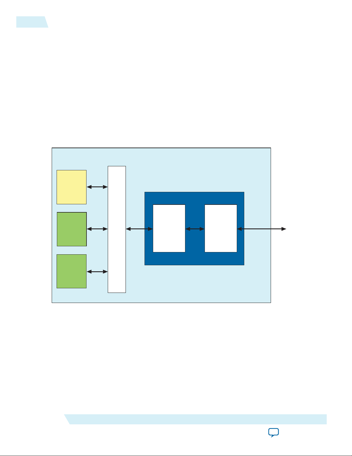
Qsys System Design V-Series Avalon-MM DMA for PCI Express
PCIe Link
Gen3 x8
DMA Engine
Avalon-MM to
PCIe TLP
Bridge
V-Series Avalon-MM DMA for PCI Express
Altera PCIe
Reconfig
Driver
Transceiver
Reconfiguration
Controller
Interconnect
2-2
Generating the Testbench
plan to replace the Descriptor Controller IP core with your own implementation, do not turn on the
Instantiate internal descriptor controller in the parameter editor when parameterizing the IP core.
Transceiver Reconfiguration Controller IP Core
The Transceiver Reconfiguration Controller performs offset cancellation to compensate for variations due
to process, voltage, and temperature (PVT).
The following provides a high-level block diagram of the V-Series Avalon-MM DMA for PCI Express
Design Example.
Altera PCIe Reconfig Driver IP Core
The PCIe Reconfig Driver drives the Transceiver Reconfiguration Controller. This driver is a plain text
Verilog HDL file that you can modify if necessary to meet your system requirements.
Block Diagram of the Avalon-MM DMA for PCI Express Example Design
UG-01154
2014.12.18
Related Information
Generating the Testbench
Altera Corporation
• V-Series Avalon-MM DMA for PCI Express on page 8-8
• DMA Descriptor Controller Registers on page 5-15
1. Copy the example design, pcie_de_ep_dma_g3x8_integrated.qsys, from the installation directory:
<install_dir>/ip/altera/altera_pcie/altera_pcie_hip_256_avmm/example_design/ to your working directory.
2. Start Qsys, by typing the following command:
Getting Started with the Avalon-MM DMA
Send Feedback
Page 17
UG-01154
2014.12.18
Generating the Testbench
qsys-edit
3. Open pcie_de_ep_dma_g3x8_integrated.qsys.
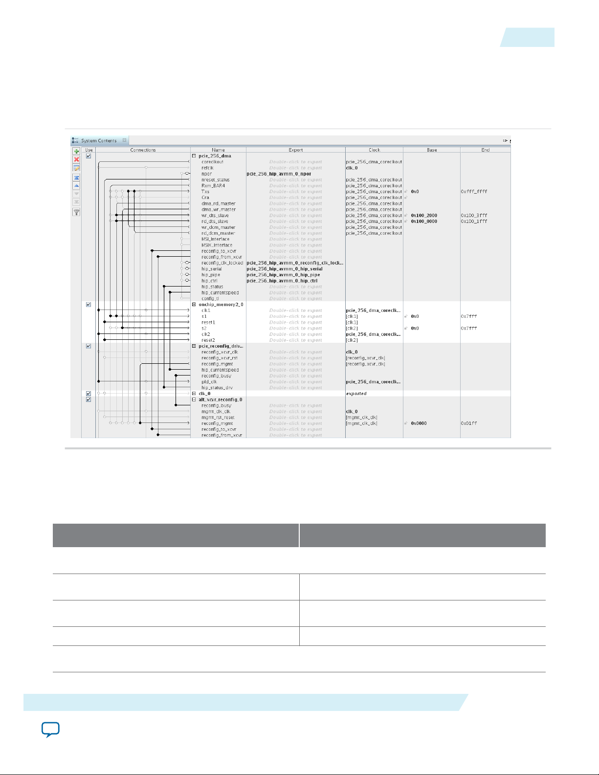
The following figure shows the Qsys system.
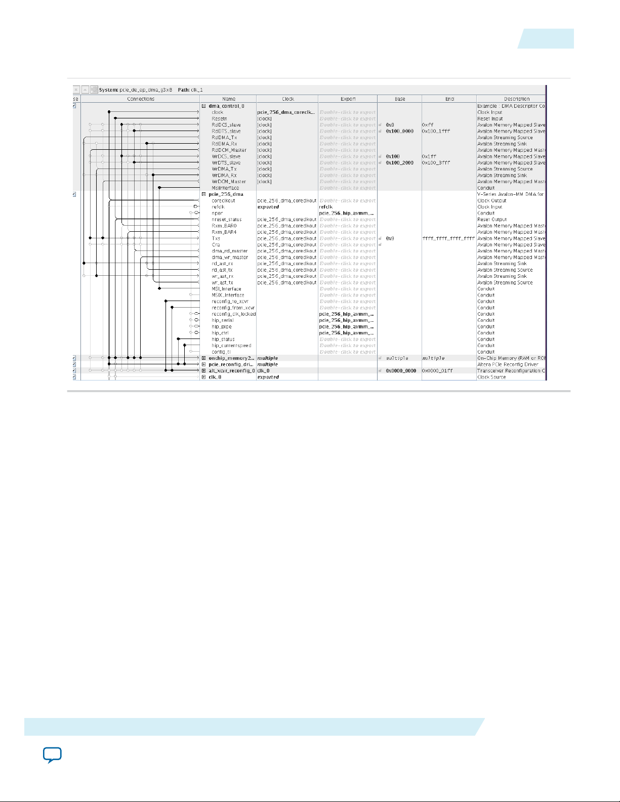
Figure 2-1: V-Series Avalon-MM DMA for PCI Express Qsys System Design
2-3
4. Click Generate > Generate Testbench System.
The Generation dialog box appears.
5. Specify the following parameters:
Table 2-1: Parameters to Specify in the Generation Dialog Box
Parameter Value
Testbench System
Create testbench Qsys system Standard, BFMs for standard Qsys interfaces
Create testbench simulation model Verilog
Allow mixed-language simulation You can leave this option off.
Output Directory
Getting Started with the Avalon-MM DMA
Send Feedback
Altera Corporation
Page 18

2-4
Understanding the Simulation Generated Files
Parameter Value
UG-01154
2014.12.18
Path
<working_dir>//pcie_de_ep_dma_g3x8_integrated
6. Click Generate.
Qsys generates the testbench.
Understanding the Simulation Generated Files
Table 2-2: Qsys Generation Output Files
Directory Description
<testbench_dir>/<variant_name>/testbench
Includes testbench subdirectories for the Aldec,
Cadence, Mentor, and Synopsys simulation tools
with the required libraries and simulation scripts.
<testbench_dir>/<variant_name>/testbench/<cad_
vendor>
<testbench_dir>/<variant_name>/testbench/<variant_
namer>_tb
Includes the HDL source files and scripts for the
simulation testbench.
Includes HDL design files
Understanding Simulation Log File Generation
Starting with the Quartus II 14.0 software release, simulation automatically creates a log file, altpcie_
monitor_<dev>_dlhip_tlp_file_log.log in your simulation directory.
Table 2-3: Sample Simulation Log File Entries
Time TLP Type Payload
(Bytes)
17989 RX CfgRd0 0004 04000001_0000000F_01080008
17989 RX MRd 0000 00000000_00000000_01080000
18021 RX CfgRd0 0004 04000001_0000010F_0108002C
18053 RX CfgRd0 0004 04000001_0000030F_0108003C
18085 RX MRd 0000 00000000_00000000_0108000C
Simulating the Example Design in ModelSim
1. In a terminal window, change directory to <workingdir>/pcie_de_ep_dma_g3x8_integrated/testbench/
mentor/ .
2. Start the ModelSim® simulator.
3. To run the simulation, type the following commands in a terminal window:
a. do msim_setup.tcl
b. ld_debug
TLP Header
Altera Corporation
Getting Started with the Avalon-MM DMA
Send Feedback
Page 19

UG-01154
2014.12.18
The ld_debug command compiles all design files and elaborates the top-level design without any
optimization.
c. run -all
The simulation performs the following operations:
• Various configuration accesses after the link is initialized
• Setup of the DMA controller to read data from the Transaction Layer Direct BFM’s shared memory
• Setup of the DMA controller to write the same data back to the Transaction Layer Direct BFM’s shared
memory
• Data comparison and report of any mismatch
Running a Gate-Level Simulation
The PCI Express testbenches run simulations at the register transfer level (RTL). However, it is possible to
create you own gate-level simulations. Contact your Altera Sales Representative for instructions and an
example that illustrate how to create a gate-level simulation from the RTL testbench.
Generating Quartus II Synthesis Files
Running a Gate-Level Simulation
2-5
1. On the Generate menu, select Generate HDL.
2. For Create HDL design files for synthesis, select Verilog.
You can leave the default settings for all other items.
3. Click Generate to generate files for Quartus II synthesis.
4. Click Finish when the generation completes.
Creating a Quartus II Project
You can create a new Quartus II project with the New Project Wizard, which helps you specify the
working directory for the project, assign the project name, and designate the name of the top-level design
entity.
1. On the Quartus II File menu, click then New Project Wizard, then Next.
2. Click Next in the New Project Wizard: Introduction (The introduction does not appear if you
previously turned it off.)
3. On the Directory, Name, Top-Level Entity page, enter the following information:
a. For What is the working directory for this project, browse to <project_dir>/pcie_de_ep_dma_g3x8_
integrated/.
b. For What is the name of this project? browse to the <project_dir>/pcie_de_ep_dma_g3x8_integrated/
synthesis directory and select pcie_de_ep_dma_g3x8_integrated.v.
c. Click Next.
4. For Project Type select Empty project.
5. Click Next.
6. On the Add Files page, add <project_dir>/pcie_de_ep_dma_g3x8_integrated/synthesis/ep_g3x8_avmm256_
integrated.qip to your Quartus II project.
7. Click Next to display the Family & Device Settings page.
Getting Started with the Avalon-MM DMA
Send Feedback
Altera Corporation
Page 20

2-6
Adding Virtual Pin Assignment to the Quartus II Settings File (.qsf)
8. On the Device page, choose the following target device family and options:
a. In the Family list, select Stratix V (GS/GT/GX/E).
b. In the Devices list, select Stratix V GX PCIe.
c. In the Available devices list, select 5SGXEA7K2F40C2.
9. Click Next to close this page and display the EDA Tool Settings page.
10.From the Simulation list, select ModelSim. From the Format list, select the HDL language you intend
to use for simulation.
11.Click Next to display the Summary page.
12.Check the Summary page to ensure that you have entered all the information correctly.
13.Click Finish.
14.Save your project.
Adding Virtual Pin Assignment to the Quartus II Settings File (.qsf)
To compile successfully you must add a virtual pin assignment statement for the PIPE interface to
your .qsf file. The PIPE interface is useful for debugging, but is not a top-level interface of the IP core.
1. Browse to the synthesis directory that includes the .qsf for your project, <project_dir>.
2. Open pcie_de_ep_dma_g3x8_integrated.qsf.
3. Add the following assignment statement:
set_instance_assignment -name VIRTUAL_PIN ON -to pcie_256_hip_avmm_0_hip_pipe_*
4. Save the .qsf file.
UG-01154
2014.12.18
Compiling the Design
1. On the Quartus II Processing menu, click Start Compilation.
2. After compilation, expand the TimeQuest Timing Analyzer folder in the Compilation Report. Note
whether the timing constraints are achieved in the Compilation Report.
If your design does not initially meet the timing constraints, you can find the optimal Fitter settings for
your design by using the Design Space Explorer. To use the Design Space Explorer, click Launch Design
Space Explorer on the Tools menu.
Descriptor Controller Connectivity when Instantiated Separately
This Qsys design example block diagram shows how to connect the external Descriptor Controller to the
Hard IP for PCI Expess with Avalon-MM DMA interface. This design example is available in <install_dir>/
ip/altera/altera_pcie/altera_pcie_hip_256_avmm/example_design/<dev>.
Altera Corporation
Getting Started with the Avalon-MM DMA
Send Feedback
Page 21
UG-01154
2014.12.18
Descriptor Controller Connectivity when Instantiated Separately
Figure 2-2: External Descriptor Controller Connectivity
2-7
Getting Started with the Avalon-MM DMA
Send Feedback
Altera Corporation
Page 22

2014.12.18
www.altera.com
101 Innovation Drive, San Jose, CA 95134
Parameter Settings
3
UG-01154
Subscribe
Send Feedback
System Settings
Table 3-1: System Settings for PCI Express
Parameter Value Description
Number of Lanes x1, x2, ×4, ×8 Specifies the maximum number of lanes supported. Avalon-
MM Interface with DMA does not support x1 configurations.
Lane Rate Gen1 (2.5 Gbps)
Gen2 (2.5/5.0 Gbps)
Gen3 (2.5/5.0/8.0
Gbps)
Application
interface width
128-bit
256-bit
Specifies the maximum data rate at which the link can operate.
Specifies the width of the interface to the Application Layer.
The following table indicates the possible combinations.
Application
Interface Width
Configuration Application Layer
Clock Frequency
128 bits Gen1 x8 125 MHz
128 bits Gen2 x4 125 MHz
128 bits Gen2 x8 250 MHz
256 bits Gen2 x8 125 MHz
128 bits Gen3 x4 250 MHz
256 bits Gen3 x4 125 MHz
256 bits Gen3 x8 250 MHz
RX Buffer credit
allocation -
©
2014 Altera Corporation. All rights reserved. ALTERA, ARRIA, CYCLONE, ENPIRION, MAX, MEGACORE, NIOS, QUARTUS and STRATIX words and logos are
trademarks of Altera Corporation and registered in the U.S. Patent and Trademark Office and in other countries. All other words and logos identified as
trademarks or service marks are the property of their respective holders as described at www.altera.com/common/legal.html. Altera warrants performance
of its semiconductor products to current specifications in accordance with Altera's standard warranty, but reserves the right to make changes to any
products and services at any time without notice. Altera assumes no responsibility or liability arising out of the application or use of any information,
product, or service described herein except as expressly agreed to in writing by Altera. Altera customers are advised to obtain the latest version of device
specifications before relying on any published information and before placing orders for products or services.
Minimum
Low
Determines the allocation of posted header credits, posted
data credits, non-posted header credits, completion header
ISO
9001:2008
Registered
Page 23

3-2
System Settings
Parameter Value Description
UG-01154
2014.12.18
performance for
received requests
Balanced
High
Maximum
credits, and completion data credits in the 16 KByte RX buffer.
The 5 settings allow you to adjust the credit allocation to
optimize your system. The credit allocation for the selected
setting displays in the message pane.
The Message window dynamically updates the number of
credits for Posted, Non-Posted Headers and Data, and
Completion Headers and Data as you change this selection.
Altera Corporation
Parameter Settings
Send Feedback
Page 24

UG-01154
2014.12.18
Parameter Value Description
• Minimum RX Buffer credit allocation -performance for
received requests )—configures the minimum PCIe
specification allowed for non-posted and posted request
credits, leaving most of the RX Buffer space for received
completion header and data. Select this option for
variations where application logic generates many read
requests and only infrequently receives single requests
from the PCIe link.
• Low—configures a slightly larger amount of RX Buffer
space for non-posted and posted request credits, but still
dedicates most of the space for received completion header
and data. Select this option for variations for which
application logic generates many read requests and
infrequently receives small bursts of requests from the
PCIe link. This option is recommended for typical
endpoint applications in which most of the PCIe traffic is
generated by a DMA engine that is located in the endpoint
application layer logic.
• Balanced—configures approximately half the RX Buffer
space to received requests and the other half of the RX
Buffer space to received completions. Select this option for
applications in which the received requests and received
completions are roughly equal.
• High—configures most of the RX Buffer space for received
requests and allocates a slightly larger than minimum
amount of space for received completions. Select this
option if most of the PCIe requests are generated by the
other end of the PCIe link and the local application layer
logic only infrequently generates a small burst of read
requests. This option is recommended for typical Root Port
applications in which most of the PCIe traffic is generated
by DMA engines located in the endpoints.
• Maximum—configures the minimum PCIe specification
allowed amount of completion space, leaving most of the
RX Buffer space for received requests. Select this option
when most of the PCIe requests are generated by the other
end of the PCIe link and the local application layer logic
never or only infrequently generates single read requests.
This option is recommended for control and status
Endpoint applications that don't generate any PCIe
requests of their own and are the target only of write and
read requests from the root complex.
System Settings
3-3
Parameter Settings
Send Feedback
Altera Corporation
Page 25

3-4
System Settings
Parameter Value Description
UG-01154
2014.12.18
Reference clock
frequency
Instantiate
internal
descriptor
controller
100 MHz
125 MHz
On/Off
The PCI Express Base Specification 3.0 requires a
100 MHz ±300 ppm reference clock. The 125 MHz reference
clock is provided as a convenience for systems that include a
125 MHz clock source. For more information about Gen3
operation, refer to 4.3.8 Refclk Specifications for 8.0 GT/s in the
specification.
For Gen3 operation, Altera recommends using a common
reference clock (0 ppm) because when using separate
reference clocks (non 0 ppm), the PCS occasionally must
insert SKP symbols, potentially causes the PCIe link to go to
recovery. Gen1 or Gen2 modes are not affected by this issue.
Systems using the common reference clock (0 ppm) are not
affected by this issue. The primary repercussion of this is a
slight decrease in bandwidth. On Gen3 x8 systems, this
bandwidth impact is negligible. If non 0 ppm mode is
required, so that separate reference clocks are being used,
please contact Altera for further information and guidance.
When you turn this option on, the descriptor controller is
included in the Avalon-MM bridge. When you turn this
option off, the descriptor controller should be included as a
separate external component. Turn this option on, if you plan
to use the Altera-provided descriptor controller in your
design. Turn this option off if you plan to modify or replace
the descriptor controller logic in your design.
Enable AvalonMM CRA Slave
hard IP status
port
Enable burst
capabilities for
RXM BAR2 port
Enable configu‐
ration via the
PCIe link
On/Off
Allows read and write access to bridge registers from the
interconnect fabric using a specialized slave port. This option
is required for Requester/Completer variants and optional for
Completer Only variants. Enabling this option allows read
and write access to bridge registers, except in the CompleterOnly single dword variations.
On/Off
When you turn on this option, the BAR2 RX Avalon-MM
masters is burst capable. If BAR2 is 32 bits and Burst capable,
then BAR3 is not available for other use. If BAR2 is 64 bits, the
BAR3 register holds the upper 32 bits of the address.
On/Off On, the Quartus II software places the Endpoint in the
location required for configuration via protocol (CvP). For
more information about CvP, click the Configuration via
Protocol (CvP) link below
Altera Corporation
Parameter Settings
Send Feedback
Page 26

UG-01154
2014.12.18
Base Address Register (BAR) Settings
Parameter Value Description
3-5
Use ATX PLL
On/Off When you turn on this option, the Hard IP for PCI Express
uses the ATX PLL instead of the CMU PLL. For other configu‐
rations, using the ATX PLL instead of the CMU PLL reduces
the number of transceiver channels that are necessary. This
option requires the use of the soft reset controller and does not
support the CvP flow.
Enable Hard IP
reset pulse at
power-up when
using the soft
reset controller
On/Off
When you turn on this option, the soft reset controller
generates a pulse at power up to reset the Hard IP. This pulse
ensures that the Hard IP is reset after programming the
device, regardless of the behavior of the dedicated PCI Express
reset pin, perstn. This option is available for Gen2 and Gen3
designs that use a soft reset controller.
Base Address Register (BAR) Settings
The type and size of BARs available depend on port type.
Table 3-2: BAR Registers
Parameter Value Description
Type Disabled
64-bit prefetchable memory
32-bit non-prefetchable memory
32-bit prefetchable memory
I/O address space
Size
N/A Qsys automatically calculates the required size after
If you select 64-bit prefetchable memory, 2
contiguous BARs are combined to form a 64-bit
prefetchable BAR; you must set the higher numbered
BAR to Disabled.
Defining memory as prefetchable allows contiguous
data to be fetched ahead. Prefetching memory is
advantageous when the requestor may require more
data from the same region than was originally
requested. If you specify that a memory is prefetch‐
able, it must have the following 2 attributes:
• Reads do not have side effects
• Write merging is allowed
The 32-bit prefetchable memory and I/O address
space BARs are only available for the Legacy
Endpoint.
you connect your components.
Parameter Settings
Send Feedback
Altera Corporation
Page 27

3-6
Device Identification Registers
UG-01154
2014.12.18
Device Identification Registers
Table 3-3: Device ID Registers
The following table lists the default values of the read-only Device ID registers. You can use the parameter editor
to change the values of these registers. Refer to Type 0 Configuration Space Registers for the layout of the Device
Identification registers.
Register Name Range Default Value Description
Vendor ID 16 bits 0x00000000
Sets the read-only value of the Vendor ID register. This
parameter can not be set to 0xFFFF per the PCI Express
Specification.
Address offset: 0x000.
Device ID 16 bits 0x00000001 Sets the read-only value of the Device ID register.
Address offset: 0x000.
Revision ID 8 bits 0x00000001 Sets the read-only value of the Revision ID register.
Address offset: 0x008.
Class code 24 bits 0x00000000 Sets the read-only value of the Class Code register.
Address offset: 0x008.
Subsystem
Vendor ID
16 bits 0x00000000 Sets the read-only value of the Subsystem Vendor ID
register in the PCI Type 0 Configuration Space. This
parameter cannot be set to 0xFFFF per the PCI Express
Base Specification. This value is assigned by PCI-SIG to
the device manufacturer.
Address offset: 0x02C.
Subsystem
Device ID
16 bits 0x00000000 Sets the read-only value of the Subsystem Device ID
register in the PCI Type 0 Configuration Space.
Address offset: 0x02C
Related Information
PCI Express Base Specification 2.1 or 3.0
PCI Express and PCI Capabilities Parameters
This group of parameters defines various capability properties of the IP core. Some of these parameters
are stored in the PCI Configuration Space - PCI Compatible Configuration Space. The byte offset
indicates the parameter address.
Altera Corporation
Parameter Settings
Send Feedback
Page 28

UG-01154
2014.12.18
Device Capabilities
Table 3-4: Capabilities Registers
Parameter Possible Values Default Value Description
Device Capabilities
3-7
Maximum
payload size
128 bytes
256 bytes
128 bytes Specifies the maximum payload size supported. This
parameter sets the read-only value of the max payload
size supported field of the Device Capabilities register
(0x084[2:0]). Address: 0x084.
Implement
completion
timeout
disable
On/Off On For Endpoints using PCI Express version 2.1 or 3.0, this
option must be On. The timeout range is selectable.
When On, the core supports the completion timeout
disable mechanism via the PCI Express Device
Control Register 2. The Application Layer logic must
implement the actual completion timeout mechanism
for the required ranges.
Error Reporting
Table 3-5: Error Reporting
Parameter Value Default Value Description
Advanced
error
reporting
(AER)
On/Off Off When On, enables the Advanced Error Reporting (AER)
capability.
ECRC
checking
ECRC
generation
Note:
1. Throughout this user guide, the terms word, dword and qword have the same meaning that they have
in the PCI Express Base Specification. A word is 16 bits, a dword is 32 bits, and a qword is 64 bits.
Related Information
PCI Express Base Specification Revision 2.1 or 3.0
Parameter Settings
Send Feedback
On/Off Off When On, enables ECRC checking. Sets the read-only
value of the ECRC check capable bit in the Advanced
Error Capabilities and Control Register. This
parameter requires you to enable the AER capability.
On/Off Off
When On, enables ECRC generation capability. Sets the
read-only value of the ECRC generation capable bit in
the Advanced Error Capabilities and Control
Register. This parameter requires you to enable the
AER capability.
Altera Corporation
Page 29

3-8
Link Capabilities
Link Capabilities
Table 3-6: Link Capabilities
Parameter Value Description
UG-01154
2014.12.18
Link port
number
Slot clock
configuration
0x01 Sets the read-only value of the port number field in the Link
Capabilities register.
On/Off When On, indicates that the Endpoint or Root Port uses the
same physical reference clock that the system provides on the
connector. When Off, the IP core uses an independent clock
regardless of the presence of a reference clock on the
connector.
MSI and MSI-X Capabilities
Table 3-7: MSI and MSI-X Capabilities
Parameter Value Description
MSI messages
requested
Implement MSI-X On/Off When On, enables the MSI-X functionality.
1, 2, 4, 8, 16 Specifies the number of messages the Application Layer can
request. Sets the value of the Multiple Message Capable
field of the Message Control register, 0x050[31:16].
MSI-X Capabilities
Table size [10:0] System software reads this field to determine the MSI-X Table
Table Offset [31:0] Points to the base of the MSI-X Table. The lower 3 bits of the
Table BAR
Indicator
Altera Corporation
Bit Range
size <n>, which is encoded as <n–1>. For example, a returned
value of 2047 indicates a table size of 2048. This field is readonly. Legal range is 0–2047 (211).
Address offset: 0x068[26:16]
table BAR indicator (BIR) are set to zero by software to form a
32-bit qword-aligned offset. This field is read-only.
[2:0] Specifies which one of a function’s BARs, located beginning at
0x10 in Configuration Space, is used to map the MSI-X table
into memory space. This field is read-only. Legal range is 0–5.
Parameter Settings
Send Feedback
Page 30

UG-01154
2014.12.18
Parameter Value Description
Power Management
3-9
Pending Bit Array
(PBA) Offset
[31:0] Used as an offset from the address contained in one of the
function’s Base Address registers to point to the base of the
MSI-X PBA. The lower 3 bits of the PBA BIR are set to zero by
software to form a 32-bit qword-aligned offset. This field is
read-only.
PBA BAR Indicator
[2:0] Specifies the function Base Address registers, located
beginning at 0x10 in Configuration Space, that maps the MSIX PBA into memory space. This field is read-only. Legal range
is 0–5.
Related Information
PCI Express Base Specification Revision 2.1 or 3.0
Power Management
Table 3-8: Power Management Parameters
Parameter Value Description
Endpoint L0s
acceptable
latency
Maximum of 64 ns
Maximum of 128 ns
Maximum of 256 ns
Maximum of 512 ns
Maximum of 1 us
Maximum of 2 us
Maximum of 4 us
No limit
This design parameter specifies the maximum acceptable
latency that the device can tolerate to exit the L0s state for any
links between the device and the root complex. It sets the
read-only value of the Endpoint L0s acceptable latency field of
the Device Capabilities Register (0x084).
This Endpoint does not support the L0s or L1 states. However,
in a switched system there may be links connected to switches
that have L0s and L1 enabled. This parameter is set to allow
system configuration software to read the acceptable latencies
for all devices in the system and the exit latencies for each link
to determine which links can enable Active State Power
Management (ASPM). This setting is disabled for Root Ports.
Parameter Settings
Send Feedback
The default value of this parameter is 64 ns. This is the safest
setting for most designs.
Altera Corporation
Page 31

3-10
PCIe Address Space Settings
Parameter Value Description
UG-01154
2014.12.18
Endpoint L1
Maximum of 1 us
acceptable
latency
Maximum of 2 us
Maximum of 4 us
Maximum of 8 us
Maximum of 16 us
Maximum of 32 us
No limit
PCIe Address Space Settings
Table 3-9: PCIe Address Space Settings
This value indicates the acceptable latency that an Endpoint
can withstand in the transition from the L1 to L0 state. It is an
indirect measure of the Endpoint’s internal buffering. It sets
the read-only value of the Endpoint L1 acceptable latency field
of the Device Capabilities Register.
This Endpoint does not support the L0s or L1 states. However,
a switched system may include links connected to switches
that have L0s and L1 enabled. This parameter is set to allow
system configuration software to read the acceptable latencies
for all devices in the system and the exit latencies for each link
to determine which links can enable Active State Power
Management (ASPM). This setting is disabled for Root Ports.
The default value of this parameter is 1 µs. This is the safest
setting for most designs.
Parameter Value Default Value Description
Address
width of
accessible
20–64
32
Specifies the width of the TX Slave Module Avalon-MM
address. This address is used unchanged as the PCIe
address.
PCIe
Memory
space
Altera Corporation
Parameter Settings
Send Feedback
Page 32

2014.12.18
www.altera.com
101 Innovation Drive, San Jose, CA 95134
Interfaces and Signal Descriptions
4
UG-01154
Subscribe
Send Feedback
This chapter describes the top-level signals of V-Series the Avalon-MM DMA for PCI Express IP Core.
The Avalon-MM bridge includes high-performance, burst-capable Read DMA and Write DMA modules.
You can include the DMA Descriptor Controller that controls the Read DMA and Write DMA modules
in the Avalon-MM bridge or instantiate it separately. This variant is available for the following configura‐
tions:
• Gen1 x8
• Gen2 x4
• Gen2 x8
• Gen3 x4
• Gen3 x8
V-Series DMA Avalon-MM DMA Interface to the Application Layer
The following figures illustrate the signals in the variant that includes the high-performance, burst capable
Read DMA and Write DMA modules. The first figure illustrates this variant when the DMA Descriptor
Controller is embedded in the Avalon-MM bridge. The second figure illustrates this variant when the
DMA Descriptor Controller is instantiated separately. Depending on the device, the interface to the
Application Layer can be 128 or 256 bits.
©
2014 Altera Corporation. All rights reserved. ALTERA, ARRIA, CYCLONE, ENPIRION, MAX, MEGACORE, NIOS, QUARTUS and STRATIX words and logos are
trademarks of Altera Corporation and registered in the U.S. Patent and Trademark Office and in other countries. All other words and logos identified as
trademarks or service marks are the property of their respective holders as described at www.altera.com/common/legal.html. Altera warrants performance
of its semiconductor products to current specifications in accordance with Altera's standard warranty, but reserves the right to make changes to any
products and services at any time without notice. Altera assumes no responsibility or liability arising out of the application or use of any information,
product, or service described herein except as expressly agreed to in writing by Altera. Altera customers are advised to obtain the latest version of device
specifications before relying on any published information and before placing orders for products or services.
ISO
9001:2008
Registered
Page 33
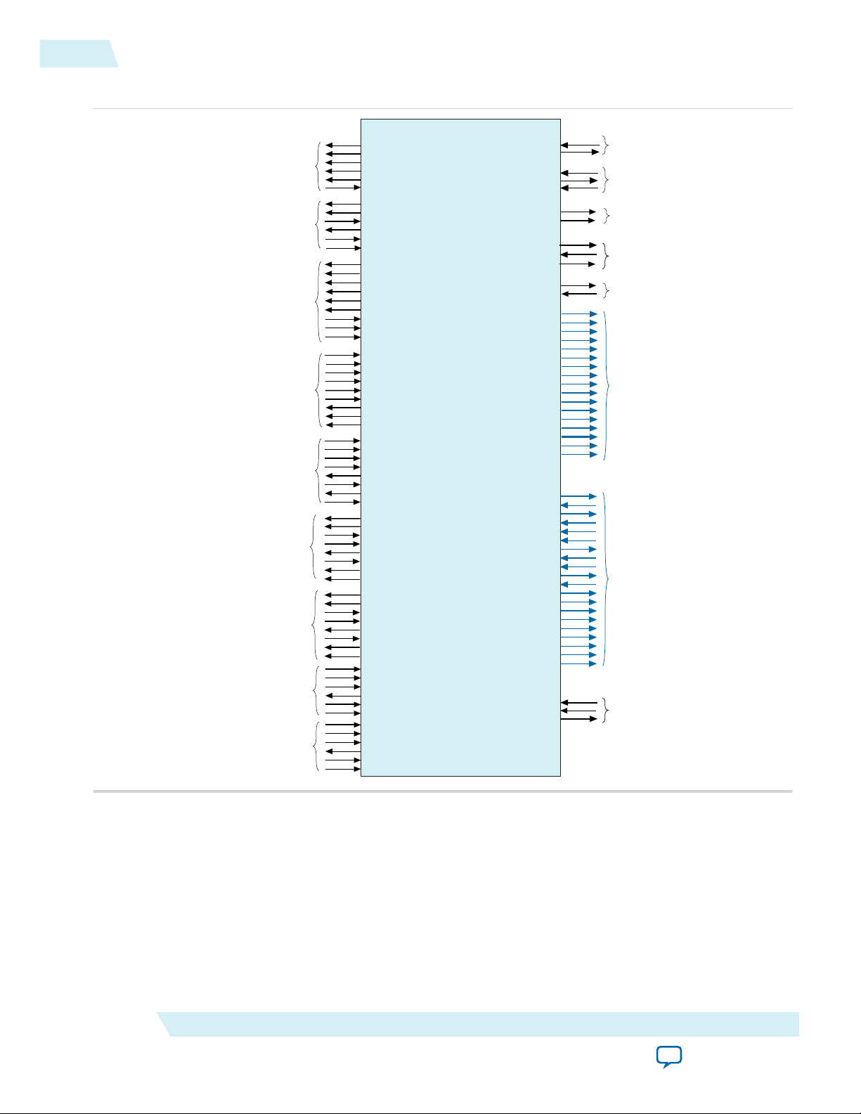
tx_out0[<n>-1:0]
rx_in0[<n>-1:0]
Hard IP Serial
Hard IP for PCI Express Using Avalon-MM with DMA
TxsWriteData_i[31:0]
TxsRead_i
TxsWrite_i
TxsChipSelect_i
TxsAddress_i[<w>-1:0]
TxsByteEnable[3:0]
TxsReadData_o[31:0]
TxsReadDataValid_o
TxsWaitRequest_o
TX Slave:
Allows FPGA to Send Single
DWord Reads or Writes
from FPGA to Root Port
RxmRead_o
RdDCMAddress_0[63:0]
RdDCMByteEnable_o[3:0]
RdDCMReadDataValid_i
RdDCMRead Data_i[31:0]
RdDCMRead_o
RdDCMWaitRequest_i
RdDCMWriteData_o[31:0]
RdDCMWrite_o
RxmWrite_o
RxmAddress_o[<w>-1:0]
RxmBurstCount_o[5:0]
RxmByteEnable_o[3:0]
RxmWriteData_o[31:0]
RxmReadData_i[31:0]
RxmReadDataValid_i
RxmWaitRequest_i
CraWriteData_o[31:0]
CraWaitRequest_o
CraChipSelect_i
CraByteEnable_i[3:0]
CraAddress_i[13:0]
CraRead
CraWrite
CraReadData[31:0]
Host Access to
Control/Status Regs
of Avalon-MM Bridge
MsiIntfc_o[81:0]
MsixIntfc_o[15:0]
RdDmaWrite_o
RdDmaAddress_o[63:0]
RdDmaWriteData[<w>-1:0]
RdDmaBurstCount_o[4:0]
RdDmaWriteEnable_o[<w>-1:0]
RdDmaWaitRequest_i
Read DMA Avalon-MM :
Writes data from Host
memory to FPGA memory.
WrDmaRead_o
WrDmaAddress_o[63:0]
WrDmaReadData_i[<w>-1:0]
WrDmaBurstCount_o[<w>-1:0]
WrDmaWaitRequest_i
WrDmaReadDataValid_i
Write DMA Avalon-MM :
Fetch data from FPGA memory
before sending to Host memory.
MSI Inter face
npor
nreset_status
pin_perst
Reset &
Lock Status
Clocks
refclk
coreclkout
<w> = 32 or 64
Avalon-MM Master
Rd Descriptor Controller
Avalon-MM Master
Drives TX Slave to
Perform Single DWord
Transactions
to the Hard IP for PCIe
for Host to Access
Registers and Memory
1 RX Master for Each
BAR
cfg_par_err
derr_cor_ext_rcv
derr_cor_ext_rpl
derr_rpl
dlup
dlup_exit
ev128ns
ev1us
hotrst_exit
int_status[3:0]
ko_clp_spc_data[11:0]
ko_cpl_spc_header[7:0]
l2_exit
lane_act[3:0]
ltssmstate[4:0]
rx_par_err
tx_par_err
Hard IP Status
Hard IP Control &
Current Speed
Interfaces
test_in[31:0]
simu_mode_pipe
current_speed[1:0]
PIPE
(simulation
only)
reconfig_from_xcvr[<n>46-1:0]
reconfig_to_xcvr[<n>70-1:0]
reconfig_clk_locked
Transceiver
Reconfiguration
not required for
Arria 10
eidleinfersel[2:0]
phystatus0
powerdown0[1:0]
rxdata0[31:0]
rxdatak0
rxelecidle0
rxpolarity
rxstatus0[2:0]
rxvalid0
sim_ltssmstate[4:0]
sim_pipe_pclk_in
sim_pipe_rate[1:0]
txcompl0
txdata[<w>-1:0]
txdatak0
txdeemph0
txdetectrx0
txelecidle0
txmargin0
txswing
WrDCMAddress_0[63:0]
WrDCMByteEnable_o[3:0]
WrDCMReadDataValid_i
WrDCMRead Data_i[31:0]
WrDCMRead_o
WrDCMWaitRequest_i
WrDCMWriteData_o[31:0]
WrDCMWrite_o
WrDTSAddress_i[7:0]
WrDTSBurstCount_i[4:0]
WrDTSChipSelect_i
WrDTXWaitRequest_o
WrDTSWriteData_i[255:0]
WrDTSWrite_i
Wr Descriptor Controller
Avalon-MM Master
Drives TX Slave to
Perform Single DWord
Transactions
to the Hard IP for PCIe
Descriptor Controller
Avalon-MM Slave
Receives Requested
Write Descriptors from the
DMA Read Master
Descriptor Controller
Avalon-MM Slave
Receives Requested
Read Descriptors from the
DMA Read Master
RdDTSAddress_i[7:0]
RdDTSBurstCount_i[4:0]
RdDTSChipSelect_i
RdDTXWaitRequest_o
RdDTSWriteData_o[255:0]
RdDTSWrite_i
4-2
V-Series DMA Avalon-MM DMA Interface to the Application Layer
Figure 4-1: Signals When Descriptor Controller Is Embedded in the Avalon-MM Bridge
UG-01154
2014.12.18
Altera Corporation
Interfaces and Signal Descriptions
Send Feedback
Page 34

tx_out0[<n>-1:0]
rx_in0[<n>-1:0]
Hard IP Serial
Hard IP for PCI Express Using Avalon-MM with DMA
TxsWriteData_i[31:0]
TxsRead_i
TxsWrite_i
TxsChipSelect_i
TxsAddress_i[<w>-1:0]
TxsByteEnable[3:0]
TxsReadData_o[31:0]
TxsReadDataValid_o
TxsWaitRequest_o
TX Slave:
Allows FPGA to send single
dword reads or writes
from FPGA to Root Port
RxmRead_o
RxmWrite_o
RxmAddress_o[<w>-1:0]
RxmBurstCount_o[5:0]
RxmByteEnable_o[3:0]
RxmWriteData_o[31:0]
RxmReadData_i[31:0]
RxmReadDataValid_i
RxmWaitRequest_i
CraWriteData_o[31:0]
CraWaitRequest_o
CraChipSelect_i
CraByteEnable_i[3:0]
CraAddress_i[13:0]
CraRead
CraWrite
CraReadData[31:0]
Local Avalon-MM or
Host Access to
Control/Status Regs
of Avalon-MM Bridge
MsiIntfc_o[81:0]
MSIxIntfc_o[15:0]
RdDmaWrite_o
RdDmaAddress_o[63:0]
RdDmaWriteData[<w>-1:0]
RdDmaBurstCount_o[<w>-1:0]
RdDmaWriteEnable_o[<w>-1:0]
RdDmaWaitRequest_i
DMA Read Avalon-MM :
Writes data from Host
memory to FPGA memory.
WrDmaRead_o
WrDmaAddress_o[63:0]
WrDmaReadData_i[<w>-1:0]
WrDmaBurstCount_o[<w>-1:0]
WrDmaWaitRequest_i
WrDmaReadDataValid_i
DMA Write Avalon-MM :
Fetch data from FPGA memory
before sending to Host memory.
MSI and MSI-X
Interface
npor
reset_status
pin_perst
Reset &
Lock Status
Clocks
refclk
coreclkout
<w> = 32 or 64
Avalon-MM Master
for Host to access
registers and memory
1 RX Master for each
BAR
cfg_par_err
derr_cor_ext_rcv
derr_cor_ext_rpl
derr_rpl
dlup
dlup_exit
ev128ns
ev1us
hotrst_exit
int_status[3:0]
ko_cpl_spc_data[11:0]
ko_cpl_spc_header[7:0]
l2_exit
lane_act[3:0]
ltssmstate[4:0]
rx_par_err
tx_par_err
Hard IP Reset,
Status and
Link Training
Hard IP Control &
Current Speed
Interfaces
test_in[31:0]
simu_mode_pipe
current_speed[1:0]
tl_cfg_add[3:0]
tl_cfg_ctl[31:0]
tl_cfg_sts[52:0]
PIPE
(simulation
only)
reconfig_from_xcvr[<n>46-1:0]
reconfig_to_xcvr[<n>70-1:0]
reconfig_clk_locked
Transaction Layer
Transceiver
Reconfiguration
Configuration
eidleinfersel0[2:0]
phystatus0
powerdown0[1:0]
rxdata0[31:0]
rxdatak0
rxelecidle0
rxpolarity
rxstatus0[2:0]
rxvalid0
sim_ltssmstate[4:0]
sim_pipe_pclk_in
sim_pipe_rate[1:0]
txcompl0
txdata[<w>-1:0]
txdatak0
txdeemph0
txdetectrx0
txelecidle0
txmargin0
txswing
Host or
RdDmaRxData_i[159:0]
RdDmaRxValid_i
RdDmaRxReady_o
WrDmaRxData_i[159:0]
WrDmaRxValid_i
WrDmaRxReady_o
WrDmaTxData_o[31:0]
WrDmaTxValid_o
Descriptor Instructions
from
Descriptor Controller
to DMA Engine
RdDmaTxData_o[31:0]
RdDmaTxValid_o
UG-01154
2014.12.18
Read DMA Avalon-MM Master Port
Figure 4-2: Signals When DMA Descriptor Controller Is Instantiated Externally
4-3
Read DMA Avalon-MM Master Port
Interfaces and Signal Descriptions
The Read DMA module sends memory read TLPs upstream. It writes the completion data to an external
Avalon-MM interface through the high throughput Read Master port. This port operates on descriptors
the IP core receives from the DMA Descriptor Controller.
Send Feedback
Altera Corporation
Page 35
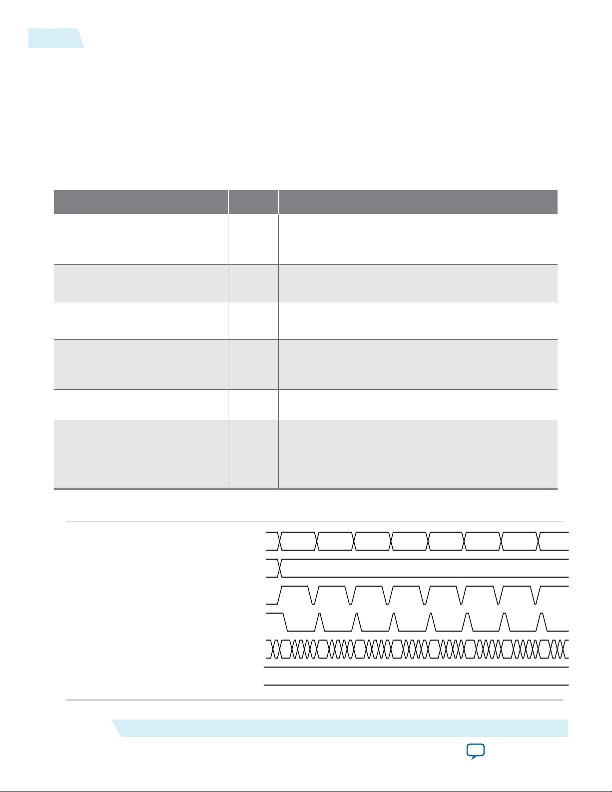
read_data_mover\.RdDmaAddress_o[63:0]
read_data_mover\.RdDmaBurstCount_o[4:0]
read_data_mover\.RdDmaWrite_o
read_data_mover\.RdDmaWaitRequest_i
read_data_mover\.RdDmaWriteData_o[255:0]
read_data_mover\.RdDmaByteEnable_o[31:0]
100 080 100 180 200 280 300 380
. . . . . . . .
4-4
Read DMA Avalon-MM Master Port
The Read DMA Avalon-MM Master Port interface performs two functions:
• Provides the descriptor table to the Descriptor Controller: This module sends memory read requests to
fetch the descriptor table from host memory using upstream memory read requests on the Avalon-ST
read interface. This module writes the descriptor entries in to the Descriptor Controller FIFO using
this 128- or 256- bit Avalon-MM interface.
• Writes data to memory located in Avalon-MM space: After a DMA Read finishes fetching data from
the source address in host memory via normal DMA-Read operation, the Read DMA module writes
the data to the destination address in Avalon-MM address space via this interface.
Table 4-1: Read DMA 256-Bit Avalon-MM Master Interface
Signal Name Direction Description
UG-01154
2014.12.18
RdDmaWrite_o
Output When asserted, indicates that the Read DMA module is
ready to write read completion data to a memory
component in the Avalon-MM address space.
RdDmaAddress_o[63:0]
Output Specifies the write address in the Avalon-MM address
space for the read completion data.
RdDmaWriteData_o[127 or
255:0]
RdDmaBurstCount_o[4:0] or
[5:0]
Output The read completion data to be written to the
Avalon-MM address space.
Output Specifies the burst count in 128- or 256-bit words. This
bus is 5 bits for the 256-bit interface. It is 6 bits for the
128-bit interface.
RdDmaByteEnable_o[15 or
31:0]
RdDmaWaitRequest_i
Output Specifies which bytes of a 128- or 256-bit word are valid.
Input When asserted, indicates that the memory is not ready to
receive data.
Frequent assertion may incoming packet processing to
stop until RdDmaWaitRequest_i deasserts.
Figure 4-3: Read DMA Avalon-MM Master Writes Data to FPGA Memory
Altera Corporation
Interfaces and Signal Descriptions
Send Feedback
Page 36
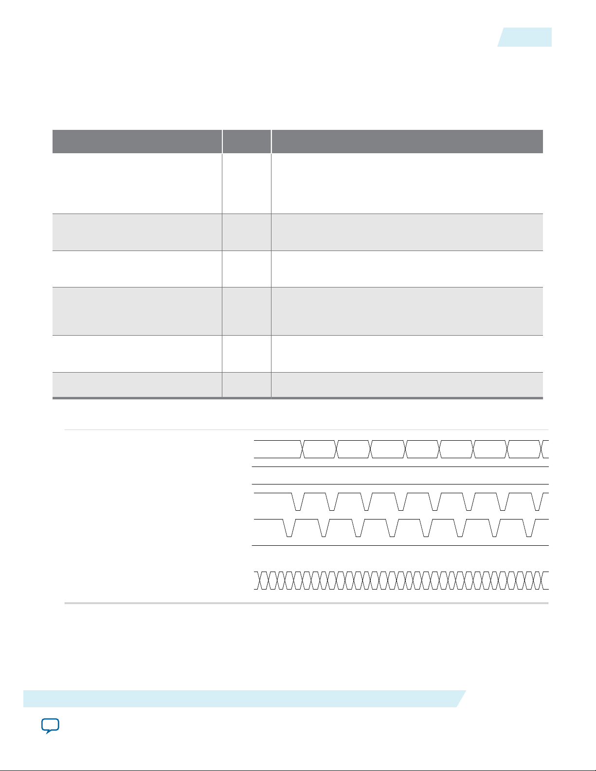
\write_data_mover.\WrDmaAddress_o[63:0]
\write_data_mover\WrDmaBurstCount_o[4:0]
\write_data_mover.\WrDmaRead_o
\write_data_mover.\WrDmaWaitRequest_i
\write_data_mover\.WrDmaReadDataValid_i
\write_data_mover.\WrDmaReadData_i[255:0]
100 180 200 280 300 380 400 480 500
UG-01154
2014.12.18
Write DMA Avalon-MM Master Port
The Write DMA module fetches data from the Avalon-MM address space using this interface before
issuing memory write requests to transfer data to host memory.
Table 4-2: DMA Read 256-Bit Avalon-MM Master Interface
Signal Name Direction Description
Write DMA Avalon-MM Master Port
4-5
WrDmaRead_o
Output When asserted, indicates that the Write DMA module
reading data from a memory component in the
Avalon-MM address space to write to the PCIe address
space.
WrDmaAddress_o[63:0]
Output Specifies the address for the data to be read from a
memory component in the Avalon-MM address space .
WrDmaReadData_i[127 or
255:0]
WrDmaBurstCount_
o[4:0]or[5:0]
Input Specifies the completion data that will be written to the
PCIe address space by the Write DMA module.
Output Specifies the burst count in 128- or 256-bit words. This
bus is 5 bits for the 256-bit interface. It is 6 bits for the
128-bit interface
WrDmaWaitRequest_i
Input When asserted, indicates that the memory is not ready to
be read.
WrDmaReadDataValid_i
Input When asserted, indicates that WrDmaReadData_i is valid.
Figure 4-4: Write DMA Avalon-MM Master Reads Data from FPGA Memory
RX Master Module
The RX Master module translates read and write TLPs received from the PCIe link to Avalon-MM
requests for Qsys components connected to the interconnect. This module allows other PCIe
components, including host software, to access other Avalon-MM slaves connected in the Qsys system.
Interfaces and Signal Descriptions
Send Feedback
Altera Corporation
Page 37

4-6
RX Master Module
If burst mode is not enabled, the RX Master module only supports 32-bit read or write request. All other
requests received from the PCIe link are considered a violation of this device’s programming model, and
are therefore handled with the PCIe Completer Abort status. You can enable burst mode for BAR2 using
32-bit addressing or BAR2 and BAR3 using 64-bit addressing. When enabled, the module supports
dword, burst read or write requests. When the Descriptor Controller is internally instantiated, the RX
Master for BAR0 is used internally and not available for other uses.
Table 4-3: RX Master Control Interface Ports for BAR Access
Each BAR has one corresponding RX Master Control interface. In this table, <n> is the BAR number.
Signal Name Direction Description
UG-01154
2014.12.18
RxmRead_<n>_o
RxmWrite_<n>_o
RxmAddress_<n>_o[<w>1:0]
RxmBurstCount_<n>_
o[5:0]
RxmByteEnable_<n>_
o[<w>:0]
RxmDataWrite_<n>_
o[<w>:0]
Output When asserted, indicates an Avalon-MM read request.
Output When asserted, indicates an Avalon-MM write request.
Output Specifies the Avalon-MM byte address. Because all addresses are
byte addresses, the meaningful bits of this address are [<w>-1:2].
Bits 1 and 0 have a value of 0. <w> can be 32 or 64.
Output Specifies the burst count in dwords (32 bits). This optional signal
is available for BAR2 when you turn on Enable burst capabili‐
ties for RXM BAR2 ports.
Output Specifies the valid bytes of data to be written. <w> has the
following values:
• 4: for the non-bursting RX Master
• 32: for the bursting 128-bit Avalon-MM interface
• 64: for the bursting 256-bit Avalon-MM interface
Output Specifies the Avalon-MM write data. <w> has the following
values:
• 32: for the non-bursting RX Master
• 128: for the bursting 128-bit Avalon-MM interface
• 256: for the bursting 256-bit Avalon-MM interface
RxmReadData_<n>_i[<w>
:0]
RxmReadDataValid_<n>_
i[31:0]
RxmWaitRequest_<n>_i
Altera Corporation
Input Specifies the Avalon-MM read data. <w> has the following
values:
• 32: for the non-bursting RX Master
• 128: for the bursting 128-bit Avalon-MM interface
• 256: for the bursting 256-bit Avalon-MM interface
Input
When asserted, indicates that RxmReadData_i[31:0]is
valid.
Input When asserted indicates that the control register access Avalon-
MM slave port is not ready to respond.
Interfaces and Signal Descriptions
Send Feedback
Page 38

AvRxmAddress_<n>_o[63:0]
AvRxmWrite_<n>_o
AvRxmWriteData_<n>_o[31:0]
AvRxmByteEnable_<n>_o[3:0]
AvRxmWaitRequest_<n>_i
AvRxmRead_<n>_o
AvRxmReadDataValid_<n>_i
AvRxmReadData_<n>_i[31:0]
800041080
00001010 00000000 00000001 00003800 00000000
8000410C 80004110 80004114 80004118 80004100
128: for the bursting 128-bit Avalon-MM interface
UG-01154
2014.12.18
Figure 4-5: RXM Master Writes To Memory in the Avalon-MM Address Space
TX Slave Module
4-7
TX Slave Module
The TX Slave module translates Avalon-MM master read and write requests to PCI Express TLPs for the
Root Port. The TX Slave Control module supports a single outstanding non-bursting request. It typically
sends status updates to the host. This is a 32-bit Avalon-MM slave bus.
Table 4-4: TX Slave Control
Signal Name Direction Description
TxsChipSelect_i
TxsRead_i
TxsWrite_i
TxsWriteData_i[<w>1:0]
TxsAddress_i[<w>-1:0]
TxsByteEnable_i[3:0]
TxsReadData_o[<w>1:0]
TxsReadDataValid_o
Input When asserted, indicates that this slave interface is selected.
Input When asserted, specifies an TX Avalon-MM slave read request
from the Root Complex or Root Port.
Input When asserted, specifies an TX Avalon-MM slave write request
to the Root Complex or Root Port.
Input Specifies the Avalon-MM data for a write command.
Input Specifies the Avalon-MM byte address for the read or write
command. The width of this address bus is specified by the
parameter Address width of accessible PCIe memory space.
Input Specifies the valid bytes for a write command.
Output Specifies the read completion data.
Output
When asserted, indicates that TxsReadData_o[31:0] is valid.
Interfaces and Signal Descriptions
Send Feedback
Altera Corporation
Page 39

AvTxsChipSelect_i
AvTxsWrite_i
AvTxsAddress_i[27:0]
AvTxsByteEnable_i[3:0]
AvTxsWriteData_i[31:0]
AvTxsWaitRequest_o
AvTxsRead_i
AvTxsReadData_o[31:0]
AvTxsReadDataValid_o
1
4-8
32-Bit Non-Bursting Avalon-MM Control Register Access (CRA) Slave Signals
Signal Name Direction Description
UG-01154
2014.12.18
TxsWaitRequest_o
Output When asserted, indicates that the Avalon-MM slave port is not
ready to respond to a read or write request.
Figure 4-6: TX Slave Interface Sends Status to Host
32-Bit Non-Bursting Avalon-MM Control Register Access (CRA) Slave Signals
Table 4-5: Avalon-MM CRA Slave Interface Signals
The CRA port provides host access to the status registers of the Avalon-MM Bridge.
Signal Name Directio
CraRead_i
CraWrite_i
CraAddress_i[13:0]
n
Input Read enable
Input Write request
Input An address space of 16 KBytes is allocated for the control
Description
registers. Avalon-MM slave addresses provide address
resolution down to the width of the slave data bus.
CraWriteData_i[31:0]
CraReadData_o[31:0]
Input Write data
Output Read data lines
Altera Corporation
Interfaces and Signal Descriptions
Send Feedback
Page 40

UG-01154
2014.12.18
Avalon-ST Descriptor Control Interface when Instantiated Separately
4-9
Signal Name Directio
CraByteEnable_i[3:0]
CraWaitRequest_o
CraChipSelect_i
CraIrq_o
Related Information
n
Input Byte enable
Output Wait request to hold off additional requests
Input Chip select signal to this slave
Output Interrupt request. A port request for an Avalon-MM interrupt.
Description
DMA Descriptor Controller Registers on page 5-15
Avalon-ST Descriptor Control Interface when Instantiated Separately
After fetching multiple descriptor entries from the Descriptor Table in the host memory, the Descriptor
Controller forms a single, 160-bit Descriptor Instruction and sends it to the Read DMA or Write DMA
engine.
Table 4-6: Descriptor Instruction Interface from Descriptor Controller to Read DMA Engine
Signal Name Direction Description
RdAstRxData_i[159:0]
Input Specifies the descriptors for the Read DMA module. Refer to
DMA Descriptor Format table below for bit definitions.
RdAstRxValid_i
RdAstRxReady_o
Input When asserted, indicates that RdAstRxData_i[159:0] is valid.
Output When asserted, indicates that the Read DMA read module is
ready to receive a new descriptor.
Table 4-7: Descriptor Instruction Interface from Descriptor Controller to Write DMA Engine
Signal Name Direction Description
WrAstRxData_i[159:0]
Input Specifies the descriptors for the Write DMA module. Refer to
DMA Descriptor Format table below for bit definitions.
WrAstRxValid_i
WrAstRxReady_o
Input When asserted, indicates that WrAstRxData_i[159:0] is valid.
Output When asserted, indicates that the Write DMA module engine is
ready to receive a new descriptor.
Interfaces and Signal Descriptions
Send Feedback
Altera Corporation
Page 41

4-10
Avalon-ST Descriptor Status Interface when Instantiated Separately
Avalon-ST Descriptor Status Interface when Instantiated Separately
When DMA module completes the processing for one Descriptor Instruction, it returns DMA Status to
the Descriptor Controller via the following interfaces.
Table 4-8: Read DMA Status Interface from Read DMA Engine to Descriptor Controller
Signal Name Direction Description
UG-01154
2014.12.18
RdAstTxData_o[31:0]
Output Drives status information to the Descriptor Controller
component. Refer to DMA Status Bus table below for more
information
RdAstTxValid_o
Output When asserted, indicates that RdAstTxData_o[31:0] is valid.
Table 4-9: Write DMA Status Interface from Write DMA Engine to Descriptor Controller
Signal Name Direction Description
WrAstTxData_o[31:0]
Output Drives status information to the Descriptor Controller
component. Refer to DMA Status Bus table below for more
information about this bus.
WwAstTxValid_o
Output When asserted, indicates that WrAstTxData_o[31:0] is valid.
Table 4-10: DMA Descriptor Format
Bits Name Description
[31:0]
Source Low Address
Low-order 32 bits of the DMA source address. The address
boundary must align to the 32 bits so that the 2 least significant
bits are 2'b00. For the Read DMA module the source address is
the PCIe domain address. For the Write DMA module the source
address is the Avalon-MM domain address. You must program
the low-order 32 bits of the address after you program the highorder 32 bits.
[63:32]
[95:64]
[127:96]
[145:12
8]
Altera Corporation
Source High Address
Destination Low Address
Destination High
Address
DMA Length
High-order 32 bits of the source address.
Low-order 32 bits of the DMA destination address. The address
boundary must align to the 32 bits so that the 2 least significant
bits have the value of 2'b00. For the Read DMA module, the
destination address is the Avalon-MM domain address. For the
Write DMA module the destination address is the PCIe domain
address.
High-order 32 bits of the destination address.
Specifies DMA length in DWords. The length must be greater
than 0. The maximum length is 1 MByte - 4 bytes.
Interfaces and Signal Descriptions
Send Feedback
Page 42

UG-01154
2014.12.18
DMA Descriptor Status Bus when Instantiated Separately
Bits Name Description
4-11
[153:14
DMA Descriptor ID
Specifies up to 128 descriptors.
6]
[159:15
Reserved
—
4]
DMA Descriptor Status Bus when Instantiated Separately
Read DMA and Write DMA modules report status to the Descriptor Controller on the RdDmaTx-
Data_o[31:0] or WrDmaTxData_o[31:0] bus when one of the following trigger events occurs:
• A descriptor is activated
• A descriptor completes successfully
The following table shows the mappings of the triggering events to the DMA descriptor status bus:
Table 4-11: DMA Status Bus
Bits Name Description
[31:9] Reserved. —
[8]
Done
When asserted, a single DMA descriptor has completed success‐
fully.
[7:0] Descriptor ID The ID of the descriptor whose status is being reported.
Descriptor Controller Interfaces when Instantiated Internally
Read Descriptor Controller Avalon-MM Master Port
The Read Descriptor Controller Avalon-MM master port drives the TX Avalon-MM slave port. This port
drives single dword transactions to the V-Series Avalon-MM DMA for PCIe. The Read Descriptor
Controller uses this port to write descriptor status to the PCIe domain and possibly to MSI when MSI
messages are enabled.
Table 4-12: Read Descriptor Controller Avalon-MM Master Interface
Signal Name Direction Description
RdDCMAddress_o[63:0]
RdDCMByteEnable_
o[3:0]
RdDCMReadDataValid_i
RdDCMReadData_o[31:0]
Output Specifies the address for the read data.
Output Specifies which data bytes are valid.
Input When asserted, indicates that the read data is valid.
Output
Drives the single dword read data.
Interfaces and Signal Descriptions
Send Feedback
Altera Corporation
Page 43

4-12
Write Descriptor Controller Avalon-MM Master Port
Signal Name Direction Description
UG-01154
2014.12.18
RdDCMRead_o
RdDCMWaitRequest_i
Output When asserted, indicates a read transaction.
Input When asserted, indicates that the Avalon-MM slave devices is
not ready to respond.
RdDCMWriteData_
o[31:0]
RdDCMWrite_o
Output Drives the single dword write data to the connected slave port.
Output
When asserted, indicates a write transaction.
Write Descriptor Controller Avalon-MM Master Port
Table 4-13: Write Descriptor Controller Avalon-MM Master Interface
The Avalon-MM Descriptor Controller Master interface is a 32-bit single-dword master with wait request
support. The Write Descriptor Controller uses this port to write status back to the PCI-Express domain and
possibly MSI when MSI messages are enabled.
Signal Name Direction Description
WrDCMAddress_o[63:0]
WrDCMByteEnable_
o[3:0]
Output Specifies the address for the write data.
Output Specifies which data bytes are valid.
WrDCMReadDataValid_i
WrRdDCMReadData_
o[31:0]
WrDCMRead_o
WrDCMWaitRequest_i
Input When asserted, indicates that the read data is valid.
Output
Holds the single dword read data.
Output When asserted, indicates a read transaction.
Input When asserted, indicates that the Avalon-MM slave device is not
ready to respond.
WrDCMWriteData_
o[31:0]
WrDCMWrite_o
Output Drives the single dword write data.
Output
When asserted, indicates a write transaction.
Read Descriptor Table Avalon-MM Slave Port
This port is available when you select the internal Descriptor Controller. It receives the Read DMA
descriptors which are fetched by Read DMA. . Connect the port to the Read DMA Avalon-MM master
port.
Altera Corporation
Interfaces and Signal Descriptions
Send Feedback
Page 44

UG-01154
2014.12.18
Table 4-14: Read Descriptor Controller Avalon-MM Master Interface
Signal Name Direction Description
Write Descriptor Table Avalon-MM Slave Port
4-13
RdDTSAddress_i[7:0]
RdDTSBurstCount_
i[4:0] or [5:0]
RdDTSChipSelect_i
RdDTSWaitRequest_o
Input Specifies the descriptor address.
Input Specifies the burst count in 128- or 256-bit words.
Input When asserted, indicates that the read targets this slave port.
Output When asserted, indicates that the Avalon-MM slave device is not
ready to respond.
RdDTSWriteData_
i[255:0] or [127:0]
RdDTSWrite_i
Input Drives the 128- or 256-bit write data.
Input
When asserted, indicates a write transaction.
Write Descriptor Table Avalon-MM Slave Port
Table 4-15: Write Descriptor Controller Avalon-MM Master Interface
Host software writes descriptors to the Avalon-MM slave port of the descriptor table. This port connects to a
bursting DMA write master interface.
Signal Name Direction Description
WrDTSAddress_i[7:0]
Input Specifies the descriptor address for the write data.
WrDTSBurstCount_
i[4:0] or [5:0]
WrDTSChipSelect_i
WrDTSWaitRequest_o
WrDTSWriteData_
i[255:0] or [127:0]
WrDTSWrite_i
Input Specifies the burst count in 128- or 256-bit words.
Input When asserted, indicates that the write is for this slave port.
Output When asserted, indicates that the Avalon-MM slave device is not
ready to respond.
Input Drives the 128- or 256-bit write data.
Input
When asserted, indicates a write transaction.
Interfaces and Signal Descriptions
Send Feedback
Altera Corporation
Page 45

4-14
Clock Signals
Clock Signals
Table 4-16: Clock Signals
Signal Direction Description
UG-01154
2014.12.18
refclk
coreclkout
Input Reference clock for the IP core. It must have the frequency
specified under the System Settings heading in the parameter
editor. This is a dedicated free running input clock to the
dedicated REFCLK pin.
If your design meets the following criteria:
• Enables CvP
• Includes an additional transceiver PHY connected to the same
Transceiver Reconfiguration Controller
then you must connect refclk to the mgmt_clk_clk signal of the
Transceiver Reconfiguration Controller and the additional
transceiver PHY. In addition, if your design includes more than
one Transceiver Reconfiguration Controller on the same side of
the FPGA, they all must share the mgmt_clk_clk signal.
Output This is a fixed frequency clock used by the Data Link and
Transaction Layers. To meet PCI Express link bandwidth
constraints, this clock has minimum frequency requirements as
listed in Application Layer Clock Frequency for All Combination
of Link Width, Data Rate and Application Layer Interface Width
in the Reset and Clocks chapter .
Related Information
Clocks on page 6-5
Reset, Status, and Link Training Signals
Refer to Reset and Clocks for more information about the reset sequence and a block diagram of the reset
logic.
Altera Corporation
Interfaces and Signal Descriptions
Send Feedback
Page 46

UG-01154
2014.12.18
Table 4-17: Reset Signals
Signal Direction Description
Reset, Status, and Link Training Signals
4-15
npor
nreset_status
pin_perst
Input Active low reset signal. In the Altera hardware example designs,
npor is the OR of pin_perst and local_rstn coming from the
software Application Layer. If you do not drive a soft reset signal
from the Application Layer, this signal must be derived from
pin_perst. You cannot disable this signal. Resets the entire IP
Core and transceiver. Asynchronous.
In systems that use the hard reset controller, this signal is edge,
not level sensitive; consequently, you cannot use a low value on
this signal to hold custom logic in reset. For more information
about the hard and soft reset controllers, refer to Reset.
Output
Active low reset signal. It is derived from npor or pin_perstn.
You can use this signal to reset the Application Layer.
Input Active low reset from the PCIe reset pin of the device. pin_perst
resets the datapath and control registers. Configuration via
Protocol (CvP) requires this signal. For more information about
CvP refer to Configuration via Protocol (CvP).
V-Series devices can have up to 4 instances of the Hard IP for
PCI Express. Each instance has its own pin_perst signal. You
must connect the pin_perst of each Hard IP instance to the
corresponding nPERST pin of the device. These pins have the
following locations:
Interfaces and Signal Descriptions
• NPERSTL0: bottom left Hard IP and CvP blocks
• NPERSTL1: top left Hard IP block
• NPERSTR0: bottom right Hard IP block
• NPERSTR1: top right Hard IP block
For example, if you are using the Hard IP instance in the bottom
left corner of the device, you must connect pin_perst to
NPERSL0.
For maximum use of the V-Series device, Altera recommends
that you use the bottom left Hard IP first. This is the only
location that supports CvP over a PCIe link. If your design does
not require CvP, you may select other Hard IP blocks.
Refer to the appropriate device pinout for correct pin assignment
for more detailed information about these pins. The PCI Express
Card Electromechanical Specification 2.0 specifies this pin
requires 3.3 V. You can drive this 3.3V signal to the nPERST*
Altera Corporation
Send Feedback
Page 47
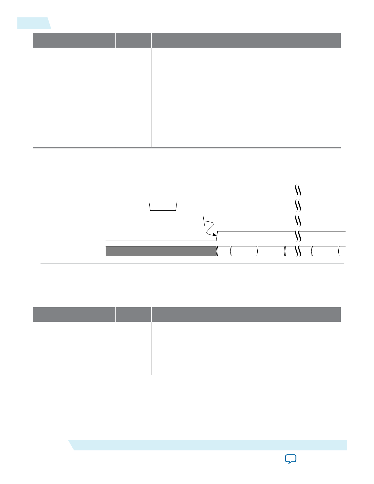
npor
IO_POF_Load
PCIe_LinkTraining_Enumeration
dl_ltssm[4:0]
detect
detect.active polling.active
L0
4-16
Reset, Status, and Link Training Signals
Signal Direction Description
UG-01154
2014.12.18
even if the V
VCCPGM
of the bank is not 3.3V if the following 2
conditions are met:
• The input signal meets the VIH and VIL specification for
LVTTL.
• The input signal meets the overshoot specification for 100°C
operation as specified by the “Maximum Allowed Overshoot
and Undershoot Voltage” section in volume 3 of the Stratix V
Device Handbook.
• The input signal meets the overshoot specification for 100°C
operation as defined in the device handbook.
Figure 4-7: Reset and Link Training Timing Relationships
The following figure illustrates the timing relationship between npor and the LTSSM L0 state.
Note: To meet the 100 ms system configuration time, you must use the fast passive parallel configuration
Table 4-18: Status and Link Training Signals
cfg_par_err
Altera Corporation
scheme with CvP and a 32-bit data width (FPP x32) or use the CvP in autonomous mode.
Signal Direction Description
Output Indicates that a parity error in a TLP routed to the internal
Configuration Space. This error is also logged in the Vendor
Specific Extended Capability internal error register. You must
reset the Hard IP if this error occurs.
The signal is not available for Arria V and Cyclone V devices.
Interfaces and Signal Descriptions
Send Feedback
Page 48

UG-01154
2014.12.18
Reset, Status, and Link Training Signals
Signal Direction Description
derr_cor_ext_rcv Output Indicates a corrected error in the RX buffer. This signal is for
debug only. It is not valid until the RX buffer is filled with data.
This is a pulse, not a level, signal. Internally, the pulse is
generated with the 500 MHz clock. A pulse extender extends the
signal so that the FPGA fabric running at 250 MHz can capture
it. Because the error was corrected by the IP core, no Application
Layer intervention is required.
derr_cor_ext_rpl Output Indicates a corrected ECC error in the retry buffer. This signal is
(8)
for debug only. Because the error was corrected by the IP core,
no Application Layer intervention is required.
(8)
4-17
derr_rpl Output Indicates an uncorrectable error in the retry buffer. This signal is
for debug only.
(8)
The signal is not available for Arria V and Cyclone V devices.
dlup
Output When asserted, indicates that the Hard IP block is in the Data
Link Control and Management State Machine (DLCMSM) DL_
Up state.
dlup_exit
Output This signal is asserted low for one pld_clk cycle when the IP
core exits the DLCMSM DL_Up state, indicating that the Data
Link Layer has lost communication with the other end of the
PCIe link and left the Up state. When this pulse is asserted, the
Application Layer should generate an internal reset signal that is
asserted for at least 32 cycles.
ev128ns
ev1us
hotrst_exit
Output Asserted every 128 ns to create a time base aligned activity.
Output Asserted every 1µs to create a time base aligned activity.
Output Hot reset exit. This signal is asserted for 1 clock cycle when the
LTSSM exits the hot reset state. This signal should cause the
Application Layer to be reset. This signal is active low. When this
pulse is asserted, the Application Layer should generate an
internal reset signal that is asserted for at least 32 cycles.
(8)
Altera does not rigorously test or verify debug signals. Only use debug signals to observe behavior. Do
not use debug signals to drive custom logic.
Interfaces and Signal Descriptions
Send Feedback
Altera Corporation
Page 49

4-18
Reset, Status, and Link Training Signals
Signal Direction Description
UG-01154
2014.12.18
int_status[3:0]
ko_cpl_spc_data[11:0]
ko_cpl_spc_
header[7:0]
l2_exit
Output These signals drive legacy interrupts to the Application Layer as
follows:
• int_status[0]: interrupt signal A
• int_status[1]: interrupt signal B
• int_status[2]: interrupt signal C
• int_status[3]: interrupt signal D
Output The Application Layer can use this signal to build circuitry to
prevent RX buffer overflow for completion data. Endpoints must
advertise infinite space for completion data; however, RX buffer
space is finite. ko_cpl_spc_data is a static signal that reflects the
total number of 16 byte completion data units that can be stored
in the completion RX buffer.
Output The Application Layer can use this signal to build circuitry to
prevent RX buffer overflow for completion headers. Endpoints
must advertise infinite space for completion headers; however,
RX buffer space is finite. ko_cpl_spc_header is a static signal
that indicates the total number of completion headers that can be
stored in the RX buffer.
Output L2 exit. This signal is active low and otherwise remains high. It is
asserted for one cycle (changing value from 1 to 0 and back to 1)
after the LTSSM transitions from l2.idle to detect. When this
pulse is asserted, the Application Layer should generate an
internal reset signal that is asserted for at least 32 cycles.
lane_act[3:0] Output Lane Active Mode: This signal indicates the number of lanes that
ltssmstate[4:0]
Altera Corporation
configured during link training. The following encodings are
defined:
• 4’b0001: 1 lane
• 4’b0010: 2 lanes
• 4’b0100: 4 lanes
• 4’b1000: 8 lanes
Output LTSSM state: The LTSSM state machine encoding defines the
following states:
• 00000: Detect.Quiet
• 00001: Detect.Active
• 00010: Polling.Active
• 00011: Polling.Compliance
• 00100: Polling.Configuration
• 00101: Polling.Speed
Interfaces and Signal Descriptions
Send Feedback
Page 50

UG-01154
2014.12.18
Reset, Status, and Link Training Signals
Signal Direction Description
• 00110: config.Linkwidthstart
• 00111: Config.Linkaccept
• 01000: Config.Lanenumaccept
• 01001: Config.Lanenumwait
• 01010: Config.Complete
• 01011: Config.Idle
• 01100: Recovery.Rcvlock
• 01101: Recovery.Rcvconfig
• 01110: Recovery.Idle
• 01111: L0
• 10000: Disable
• 10001: Loopback.Entry
• 10010: Loopback.Active
• 10011: Loopback.Exit
• 10100: Hot.Reset
• 10101: L0s
• 11001: L2.transmit.Wake
• 11010: Speed.Recovery
• 11011: Recovery.Equalization, Phase 0
• 11100: Recovery.Equalization, Phase 1
• 11101: Recovery.Equalization, Phase 2
• 11110: recovery.Equalization, Phase 3
4-19
rx_par_err
tx_par_err[1:0]
Output When asserted for a single cycle, indicates that a parity error was
detected in a TLP at the input of the RX buffer. This error is
logged as an uncorrectable internal error in the VSEC registers.
For more information, refer to Uncorrectable Internal Error
Status Register. You must reset the Hard IP if this error occurs
because parity errors can leave the Hard IP in an unknown state.
The signal is not available for Arria V and Cyclone V devices.
Output When asserted for a single cycle, indicates a parity error during
TX TLP transmission. These errors are logged in the VSEC
register. The following encodings are defined:
• 2’b10: A parity error was detected by the TX Transaction
Layer. The TLP is nullified and logged as an uncorrectable
internal error in the VSEC registers. For more information,
refer to Uncorrectable Internal Error Status Register.
• 2’b01: Some time later, the parity error is detected by the TX
Data Link Layer which drives 2’b01 to indicate the error.
Reset the IP core when this error is detected. Contact Altera
technical support if resetting becomes unworkable.
Interfaces and Signal Descriptions
Send Feedback
Altera Corporation
Page 51

4-20
MSI Interrupts for Endpoints
Signal Direction Description
Related Information
• Reset and Clocks on page 6-1
• Clocks on page 6-5
• PCI Express Card Electromechanical Specification 2.0
• Configuration via Protocol (CvP) Implementation in Altera FPGAs User Guide
MSI Interrupts for Endpoints
The MSI interrupt notifies the host when a DMA operation has completed. After the host receives this
interrupt, it can poll the DMA read or write status table to determine which entry or entries have the done
bit set. This mechanism allows host software to avoid continuous polling of the status table done bits.
UG-01154
2014.12.18
Note that not all simulation models assert the Transaction Layer
error bit in conjunction with the Data Link Layer error bit.
The signal is not available for Arria V and Cyclone V devices.
Table 4-19: MSI Interrupt
Signal Direction Description
MSIIntfc_o[81:0]
MSIXIntfc_o[15:0]
Output This bus provides the following MSI address, data, and enabled
signals:
• MSIIntfc_o[81]: Master enable
• MSIIntfc_o[80}: MSI enable
• MSIIntfc_o[79:64]: MSI data
• MSIIntfc_o[63:0]: MSI address
Output Provides for system software control of MSI-X as defined in
Section 6.8.2.3 Message Control for MSI-X in the PCI Local Bus
Specification, Rev. 3.0. The following fields are defined:
• MSIXIntfc_o[15]: Enable
• MSIXIntfc_o[14]: Mask
• MSIXIntfc_o[13:11]: Reserved
• MSIXIntfc_o[10:0]: Table size
Altera Corporation
Interfaces and Signal Descriptions
Send Feedback
Page 52

UG-01154
2014.12.18
Physical Layer Interface Signals
Signal Direction Description
4-21
MSIControl_o[15:0]
Output Provides system software control of the MSI messages as defined
in Section 6.8.1.3 Message Control for MSI in the PCI Local Bus
Specification, Rev. 3.0. The following fields are defined:
• MSIControl_o[15:9]: Reserved
• MSIControl_o[8]: Per-Vector Masking Capable
• MSIControl_o[7]: 64-Bit Address Capable
• MSIControl_o[6:4]: Multiple Message Enable
• MSIControl_o[3:1]: MSI Message Capable
• MSIControl_o[0]: MSI Enable
Physical Layer Interface Signals
Altera provides an integrated solution with the Transaction, Data Link and Physical Layers. The IP
Parameter Editor generates a SERDES variation file, <variation>_serdes.v or .vhd , in addition to the Hard
IP variation file, <variation>.v or .vhd. The SERDES entity is included in the library files for PCI Express.
Transceiver Reconfiguration
Dynamic reconfiguration compensates for variations due to process, voltage and temperature (PVT).
Among the analog settings that you can reconfigure are VOD, pre-emphasis, and equalization.
You can use the Altera Transceiver Reconfiguration Controller to dynamically reconfigure analog
settings. For more information about instantiating the Altera Transceiver Reconfiguration Controller IP
core refer to Hard IP Reconfiguration .
Table 4-20: Transceiver Control Signals
In this table, <n> is the number of interfaces required.
Signal Name Direction Description
reconfig_from_
xcvr[(<n>46)-1:0]
reconfig_to_xcvr[(<n>
70)-1:0]
reconfig_clk_locked
Output Reconfiguration signals to the Transceiver Reconfiguration
Controller.
Input Reconfiguration signals from the Transceiver Reconfiguration
Controller.
Output When asserted, indicates that the PLL that provides the fixed
clock required for transceiver initialization is locked. The
Application Layer should be held in reset until reconfig_clk_
locked is asserted.
The following table shows the number of logical reconfiguration and physical interfaces required for
various configurations. The Quartus II Fitter merges logical interfaces to minimize the number of physical
interfaces configured in the hardware. Typically, one logical interface is required for each channel and one
Interfaces and Signal Descriptions
Send Feedback
Altera Corporation
Page 53

4-22
Serial Data Signals
for each PLL. The ×8 variants require an extra channel for PCS clock routing and control. The ×8 variants
use channel 4 for clocking.
Table 4-21: Number of Logical and Physical Reconfiguration Interfaces
Variant Logical Interfaces
Gen2 ×4 5
Gen1 and Gen2 ×8 10
Gen3 ×4 6
Gen3 ×8 11
For more information about the Transceiver Reconfiguration Controller, refer to the Transceiver Reconfi‐
guration Controller chapter in the Altera Transceiver PHY IP Core User Guide .
Related Information
Altera Transceiver PHY IP Core User Guide
UG-01154
2014.12.18
Serial Data Signals
Table 4-22: 1-Bit Interface Signals
Signal Direction Description
(1)
(1)
Output Transmit output. These signals are the serial outputs of lanes 7–0.
Input Receive input. These signals are the serial inputs of lanes 7–0.
tx_out[7:0]
rx_in[7:0]
Note:
1. The x1 IP core only has lane 0. The x2 IP core only has lanes 1–0. The x4 IP core only has lanes 3–0.
Refer to Pin-out Files for Altera Devices for pin-out tables for all Altera devices in .pdf, .txt, and .xls
formats.
Transceiver channels are arranged in groups of six. For GX devices, the lowest six channels on the left side
of the device are labeled GXB_L0, the next group is GXB_L1, and so on. Channels on the right side of the
device are labeled GXB_R0, GXB_R1, and so on. Be sure to connect the Hard IP for PCI Express on the
left side of the device to appropriate channels on the left side of the device, as specified in the Pin-out Files
for Altera Devices.
Related Information
Pin-out Files for Altera Devices
Altera Corporation
Interfaces and Signal Descriptions
Send Feedback
Page 54

Ch5
Ch4
Ch3
Ch2
Ch1
Ch0
Ch5
Ch4
Ch3
Ch2
Ch1
Ch0
Ch5
Ch4
Ch3
Ch2
Ch1
Ch0
Ch5
Ch4
Ch3
Ch2
Ch1
Ch0
Ch5
Ch4
Ch3
Ch2
Ch1
Ch0
Ch5
Ch4
Ch3
Ch2
Ch1
Ch0
9 Ch 18 Ch
36 Ch
24 Ch
GXB_L2
GXB_L1
GXB_L0
GXB_R2
GXB_R1
GXB_R0
PCIe
Hard IP
with
CvP
PCIe
Hard
IP
Notes:
1. Green blocks are 10-Gbps channels.
2. Blue blocks are 6-Gbps channels.
UG-01154
2014.12.18
Physical Layout of Hard IP In Arria V GX/GX/SX/ST Devices
Physical Layout of Hard IP In Arria V GX/GX/SX/ST Devices
Arria V devices include one or two Hard IP for PCI Express IP cores. The following figures illustrate the
placement of the PCIe IP core, transceiver banks, and channels.
Transceiver channels are arranged in groups of six. For GX devices, the lowest six channels on the left side
of the device are labeled GXB_L0, the next group is GXB_L1, and so on. Channels on the right side of the
device are labeled GXB_R0, GXB_R1, and so on. Be sure to connect the Hard IP for PCI Express on the
left side of the device to appropriate channels on the left side of the device, as specified in the Pin-out Files
for Altera Devices.
Arria V devices include one or two Hard IP for PCI Express IP Cores. The following figures illustrates the
placement of the Hard IP for PCIe IP cores, transceiver banks and channels for the largest Arria V
devices. Note that the bottom left IP core includes the CvP functionality. Devices with a single Hard IP for
PCIe IP Core only include the bottom left core.
Figure 4-8: Transceiver Bank and Hard IP for PCI Express IP Core Locations in Arria GX and GT Devices
4-23
Interfaces and Signal Descriptions
Send Feedback
Altera Corporation
Page 55

Ch5
Ch4
Ch3
Ch2
Ch1
Ch0
Ch5
Ch4
Ch3
Ch2
Ch1
Ch0
Ch5
Ch4
Ch3
Ch2
Ch1
Ch0
Ch2
Ch1
Ch0
9 Ch
F896
9 Ch
F1152
9 Ch
F1517
GXB_L2
GXB_L1
GXB_L0
GXB_R0
Note: Blue blocks are 6 Gbps channels.
4-24
Physical Layout of Hard IP In Arria V GX/GX/SX/ST Devices
Figure 4-9: Transceiver Bank and Hard IP for PCI Express IP Core Locations in Arria SX Devices
UG-01154
2014.12.18
Altera Corporation
Interfaces and Signal Descriptions
Send Feedback
Page 56
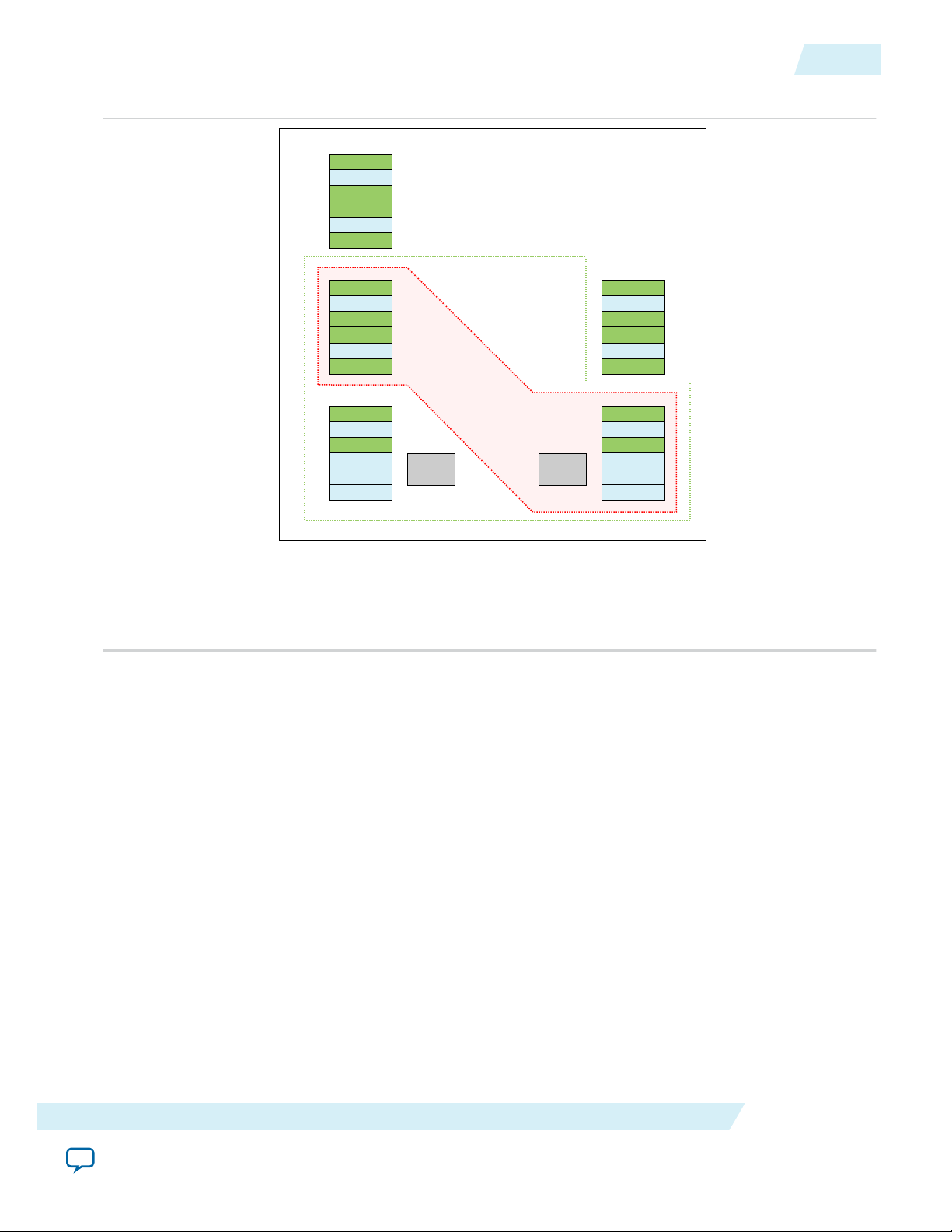
Ch5
Ch4
Ch3
Ch2
Ch1
Ch0
Ch5
Ch4
Ch3
Ch2
Ch1
Ch0
Ch5
Ch4
Ch3
Ch2
Ch1
Ch0
Ch5
Ch4
Ch3
Ch2
Ch1
Ch0
Ch5
Ch4
Ch3
Ch2
Ch1
Ch0
12 Ch
18 Ch
30 Ch
GXB_L2
GXB_L1
GXB_L0
GXB_R1
GXB_R0
HIP (1) HIP
Notes:
1. PCIe HIP availability varies with device variants.
2. Green blocks are 10-Gbps channels.
3. Blue blocks are 6-Gbps channels. With the exception of Ch0 to Ch2 in GXB_L0 and GXB_R0,
the 6-Gbps channels can be used for TX-only or RX-only 10-Gbps channels.
UG-01154
2014.12.18
Physical Layout of Hard IP In Arria V GX/GX/SX/ST Devices
Figure 4-10: Transceiver Bank and Hard IP for PCI Express IP Core Locations in Arria ST Devices
4-25
Refer to Transceiver Architecture in Arria V Devices for comprehensive information on the number of
Hard IP for PCIe IP cores available in various Arria V packages.
Related Information
• Transceiver Architecture in Arria V Devices
• Pin-Out Files for Altera Devices
Interfaces and Signal Descriptions
Altera Corporation
Send Feedback
Page 57

Ch5
Ch3
Ch2
Ch1
Ch0
CMU PLL
PCIe Hard IP
Ch0
Ch1
Ch5
Ch3
Ch2
Ch1
Ch0
CMU PLL
PCIe Hard IP
Ch0
Ch1
Ch2
Ch3
Ch5
Ch3
Ch2
Ch1
Ch0
CMU PLL
Ch0
Ch1
Ch2
Ch3
Ch11
Ch9
Ch8
Ch7
Ch6
Ch10
PCIe Hard IP
Ch5
Ch6
Ch7
Ch4
Ch5
Ch3
Ch2
CMU PLL
Ch0
Ch4
PCIe Hard IP
x1
x8
x2
x4
Ch0
4-26
Channel Placement in Arria V Devices
Channel Placement in Arria V Devices
Figure 4-11: Arria V Gen1 and Gen2 Channel Placement Using the CMU PLL
In the following figures the channels shaded in blue provide the transmit CMU PLL generating the highspeed serial clock.
UG-01154
2014.12.18
Altera Corporation
You can assign other protocols to unused channels the if data rate and clock specification exactly match
the PCIe configuration.
Physical Layout of Hard IP in Cyclone V Devices
Cyclone V devices include one or two Hard IP for PCI Express IP cores. The following figures illustrate
the placement of the PCIe IP cores, transceiver banks, and channels. Note that the bottom left IP core
includes the CvP functionality. The other Hard IP blocks do not include the CvP functionality.
Transceiver banks include six channels. Within a bank, channels are arranged in 3-packs. GXB_L0
contains channels 0–2, GXB_L1 includes channels 3–5, and so on.
Interfaces and Signal Descriptions
Send Feedback
Page 58

GXB_L0
PCIe
Hard IP
Ch 2
Ch 1
Ch 0
Ch 2
Ch 1
Ch 0
5CGXC9
GXB_L1
PCIe
Hard IP
Devices Available
Number of Channels Per Bank
Transceiver Bank Names
Ch 2
Ch 1
Ch 0
Ch 2
Ch 1
Ch 0
GXB_L2
GXB_L3
GXB_L0
PCIe
Hard IP
Ch 5
Ch 4
Ch 3
Ch 2
Ch 1
Ch 0
5CGXC4
5CGXC5
PCIe
Hard IP
Devices Available
Number of Channels Per Bank
Transceiver Bank Names
GXB_L1
UG-01154
2014.12.18
Physical Layout of Hard IP in Cyclone V Devices
Figure 4-12: Cyclone V GX/GT/ST/ST Devices with 9 or 12 Transceiver Channels and 2 PCIe Cores
In the following figure, the Hard IP for PCI Express uses channel 1 and channel 2 of GXB_L0 and channel
1 and channel 1 of GXB_L2.
4-27
Figure 4-13: Cyclone V GX/GT/ST/ST Devices with 6 Transceiver Channels and 2 PCIe Cores
For more comprehensive information about Cyclone V transceivers, refer to the Transceiver Banks
Interfaces and Signal Descriptions
Send Feedback
section in the Transceiver Architecture in Cyclone V Devices.
Related Information
Transceiver Architecture in Cyclone V Devices
Altera Corporation
Page 59

Ch5
Ch3
Ch2
Ch1
Ch0
CMU PLL
PCIe Hard IP
Ch0
Ch1
Ch5
Ch3
Ch2
Ch1
Ch0
CMU PLL
PCIe Hard IP
Ch0
Ch1
Ch2
Ch3
Ch5
Ch3
Ch2
CMU PLL
Ch0
Ch4
PCIe Hard IP
x1
x2
x4
Ch0
4-28
Channel Placement in Cyclone V Devices
Channel Placement in Cyclone V Devices
Figure 4-14: Cyclone V Gen1 and Gen2 Channel Placement Using the CMU PLL
In the following figures the channels shaded in blue provide the transmit CMU PLL generating the highspeed serial clock.
UG-01154
2014.12.18
Altera Corporation
You can assign other protocols to unused channels the if data rate and clock specification exactly match
the PCIe configuration.
Physical Layout of Hard IP in Arria V GZ Devices
Arria V GZ devices include one Hard IP for PCI Express IP core. The following figures illustrate the
placement of the PCIe IP core, transceiver banks, and channels.
Interfaces and Signal Descriptions
Send Feedback
Page 60

6 Ch
6 Ch
PCIe
Hard
IP
GXB_R2
GXB_L2
GXB_L1
GXB_L0
Ch5
Ch4
Ch3
Ch2
Ch1
Ch0
6 Ch
6 Ch
GXB_R1
GXB_R0
24
Channels
6 Ch
6 Ch
36 Channels
Notes:
1. 12-channel devices use banks L0 and L1.
2. All channels capable of backplane support up to 12.5 Gbps.
UG-01154
2014.12.18
Physical Layout of Hard IP in Stratix V GX/GT/GS Devices
Figure 4-15: Physical Layout of Hard IP in Arria V GZ Devices
4-29
Refer to Transceiver Architecture in Arria V Devices for comprehensive information on the number of
Hard IP for PCIe IP cores available in various Arria V GZ packages.
Refer to Channel Utilization for Data and Clock Routing in Arria V GZ and Stratix V Devices for
additional information about channel and PLL utilization.
Related Information
• Channel Placement in Arria V GZ and Stratix V GX/GT/GS Devices on page 4-31
• Transceiver Architecture in Arria V Devices
• Pin-Out Files for Altera Devices
Physical Layout of Hard IP in Stratix V GX/GT/GS Devices
Stratix V devices include one, two, or four Hard IP for PCI Express IP cores. The following figures
illustrate the placement of the PCIe IP cores, transceiver banks, and channels for the largest Stratix V
devices. Note that the bottom left hard IP block includes the CvP functionality for flip chip packages. For
other package types, the CvP functionality is in the bottom right block. All other Hard IP blocks do not
include the CvP functionality.
Interfaces and Signal Descriptions
Send Feedback
Altera Corporation
Page 61

3 Ch
6 Ch
6 Ch
6 Ch
6 Ch
6 Ch
3 Ch
6 Ch
6 Ch
6 Ch
6 Ch
6 Ch
PCIe
Hard
IP
PCIe
Hard
IP
PCIe
Hard
IP
IOBANK_B5R
IOBANK_B4R
IOBANK_B3R
IOBANK_B2R
IOBANK_B1R
IOBANK_B0R
IOBANK_B5L
IOBANK_B4L
IOBANK_B3L
IOBANK_B2L
IOBANK_B1L
IOBANK_B0L
Number of Channels
Per Bank
Transceiver
Bank Names
Number of Channels
Per Bank
Transceiver
Bank Names
Ch 5
Ch 4
Ch 3
Ch 2
Ch 1
Ch 0
PCIe
Hard
IP
with
CvP
4-30
Physical Layout of Hard IP in Stratix V GX/GT/GS Devices
Figure 4-16: Stratix V GX/GT/GS Devices with Four PCIe Hard IP Blocks
UG-01154
2014.12.18
Altera Corporation
Smaller devices include the following PCIe Hard IP Cores:
• One Hard IP for PCIe IP core - bottom left IP core with CvP, located at GX banks L0 and L1
• Two Hard IP for PCIe IP cores - bottom left IP core with CvP and bottom right IP Core, located at
banks L0 and L1, and banks R0 and R1
Refer to Stratix V GX/GT Channel and PCIe Hard IP (HIP) Layout for comprehensive information on the
number of Hard IP for PCIe IP cores available in various Stratix V packages.
Related Information
• Transceiver Architecture in Stratix V Devices
• Pin-Out Files for Altera Devices
Interfaces and Signal Descriptions
Send Feedback
Page 62

Ch5
Ch3
Ch2
Ch1
Ch0
ATX PLL0
CMU PLLATX PLL1
PCIe Hard IP
Ch0
Ch1
Ch5
Ch3
Ch2
Ch1
Ch0
ATX PLL0
CMU PLL
PCIe Hard IP
ATX PLL1
Ch0
Ch1
Ch2
Ch3
Ch5
Ch3
Ch2
Ch1
Ch0
ATX PLL0
CMU PLL
ATX PLL1
Ch0
Ch1
Ch2
Ch3
Ch11
Ch9
Ch8
Ch7
Ch6
Ch10
PCIe Hard IP
Ch5
Ch6
Ch7
Ch4
Ch5
Ch3
Ch2
CMU PLL
Ch0
ATX PLL0
Ch4ATX PLL1
PCIe Hard IP
x1
x8
x2
x4
Ch0
UG-01154
2014.12.18
Channel Placement in Arria V GZ and Stratix V GX/GT/GS Devices
Channel Placement in Arria V GZ and Stratix V GX/GT/GS Devices
Figure 4-17: Arria V GZ and Stratix V GX/GT/GS Gen1 and Gen2 Channel Placement Using the CMU PLL
In the following figures the channels shaded in blue provide the transmit CMU PLL generating the highspeed serial clock.
4-31
Interfaces and Signal Descriptions
Send Feedback
Altera Corporation
Page 63

Ch5
Ch3
Ch2
CMU PLL
Ch0
ATX PLL0 Gen3
Ch4
PCIe Hard IP
Ch0
Ch5
Ch3
Ch2
PCIe Hard IP
Ch0
Ch1
Ch0
Ch5
Ch3
Ch2
Ch1
Ch1
Ch0
PCIe Hard IP
Ch0
Ch1
Ch2
Ch3
ATX PLL1 Gen3
ATX PLL0
ATX PLL1 Gen3
ATX PLL0
Ch5
Ch3
Ch2
Ch1
Ch0 Ch0
Ch1
Ch2
Ch3
Ch11
Ch9
Ch8
Ch7
Ch6
Ch10
PCIe Hard IP
Ch5
Ch6
Ch7
Ch4
ATX PLL0
ATX PLL1 Gen3
ATX PLL0
CMU PLL
ATX PLL1
x1
x8
x2
x4
CMU PLL
CMU PLL
ATX PLL1
4-32
Channel Placement in Arria V GZ and Stratix V GX/GT/GS Devices
Figure 4-18: Arria V GZ and Stratix V GX/GT/GS Gen3 Channel Placement Using the CMU and ATX PLLs
Gen3 requires two PLLs to facilitate rate switching between the Gen1, Gen2, and Gen3 data rates.
Channels shaded in blue provide the transmit CMU PLL generating the high-speed serial clock. The ATX
PLL shaded in blue is the ATX PLL used in these configurations.
UG-01154
2014.12.18
Altera Corporation
Interfaces and Signal Descriptions
Send Feedback
Page 64

ATX PLL0
Ch5
Ch3
Ch2
Ch1
Ch0
ATX PLL0
Ch4
PCIe Hard IP
ATX PLL1
Ch0
Ch5
Ch3
Ch2
Ch1
Ch0
ATX PLL0
Ch4ATX PLL1
PCIe Hard IP
Ch0
Ch1
Ch5
Ch3
Ch2
Ch1
Ch0
ATX PLL0
ATX PLL0
Ch4
PCIe Hard IP
ATX PLL1
Ch0
Ch1
Ch2
Ch3
Ch5
Ch3
Ch2
Ch1
Ch0
ATX PLL0
ATX PLL1 Ch4
ATX PLL1
Ch0
Ch1
Ch2
Ch3
Ch11
Ch9
Ch8
Ch7
Ch6
Ch10
PCIe Hard IP
Ch5
Ch6
Ch7
Ch4
x1
x8
x2
x4
UG-01154
2014.12.18
PIPE Interface Signals
4-33
Figure 4-19: Arria V GZ and Stratix V GX/GT/GS Gen1 and Gen2 Channel Placement Using the ATX PLL
Selecting the ATX PLL has the following advantages over selecting the CMU PLL:
• The ATX PLL saves one channel in Gen1 and Gen2 ×1, ×2, and ×4 configurations.
• The ATX PLL has better jitter performance than the CMU PLL.
Note: You must use the soft reset controller when you select the ATX PLL and you cannot use CvP.
PIPE Interface Signals
These PIPE signals are available for Gen1, Gen2, and Gen3 variants so that you can simulate using either
the serial or the PIPE interface. Simulation is faster using the PIPE interface because the PIPE simulation
bypasses the serdes model. By default, the PIPE interface is 8 bits for Gen1 and Gen2 and 32 bits for Gen3.
You can use the PIPE interface for simulation even though your actual design includes a serial interface to
the internal transceivers. However, it is not possible to use the Hard IP PIPE interface in hardware,
including probing these signals using SignalTap® II Embedded Logic Analyzer. These signals are not toplevel signals of the Hard IP. They are listed here to assist in debugging link training issues.
Note:
Interfaces and Signal Descriptions
Send Feedback
The Altera Root Port BFM bypasses Gen3 Phase 2 and Phase 3 Equalization. However, Gen3
variants can perform Phase 2 and Phase 3 equalization if instructed by a third-party BFM.
Altera Corporation
Page 65

4-34
PIPE Interface Signals
UG-01154
2014.12.18
Table 4-23: PIPE Interface Signals
In the following table, signals that include lane number 0 also exist for lanes 1-7. These signals are for simulation
only. For Quartus II software compilation, these pipe signals can be left floating. In Qsys, the signals that are part
of the PIPE interface have the prefix, hip_pipe. The signals which are included to simulate the PIPE interface have
the prefix, hip_pipe_sim_pipe
Signal Direction Description
eidleinfersel0[2:0]
Output Electrical idle entry inference mechanism selection. The
following encodings are defined:
• 3'b0xx: Electrical Idle Inference not required in current
LTSSM state
• 3'b100: Absence of COM/SKP Ordered Set the in 128 us
window for Gen1 or Gen2
• 3'b101: Absence of TS1/TS2 Ordered Set in a 1280 UI interval
for Gen1 or Gen2
• 3'b110: Absence of Electrical Idle Exit in 2000 UI interval for
Gen1 and 16000 UI interval for Gen2
• 3'b111: Absence of Electrical idle exit in 128 us window for
Gen1
phystatus0
Input PHY status <n>. This signal communicates completion of several
PHY requests.
powerdown0[1:0] Output Power down <n>. This signal requests the PHY to change its
power state to the specified state (P0, P0s, P1, or P2).
rxdata0[31:0] Input Receive data. This bus receives data on lane <n>.
rxdatak0[3:0]
rxelecidle0 Input Receive electrical idle <n>. When asserted, indicates detection of
rxpolarity0 Output Receive polarity <n>. This signal instructs the PHY layer to
rxstatus0[2:0] Input Receive status <n>. This signal encodes receive status and error
rxvalid0 Input Receive valid <n>. This symbol indicates symbol lock and valid
Altera Corporation
Input Data/Control bits for the symbols of receive data. Bit 0
corresponds to the lowest-order byte of rxdata, and so on. A
value of 0 indicates a data byte. A value of 1 indicates a control
byte. For Gen1 and Gen2 only.
an electrical idle.
invert the polarity of the 8B/10B receiver decoding block.
codes for the receive data stream and receiver detection.
data on rxdata<n> and rxdatak <n>.
Interfaces and Signal Descriptions
Send Feedback
Page 66

UG-01154
2014.12.18
Signal Direction Description
PIPE Interface Signals
4-35
sim_pipe_
ltssmstate0[4:0]
Input and
Output
LTSSM state: The LTSSM state machine encoding defines the
following states:
• 5’b00000: Detect.Quiet
• 5’b 00001: Detect.Active
• 5’b00010: Polling.Active
• 5’b 00011: Polling.Compliance
• 5’b 00100: Polling.Configuration
• 5’b00101: Polling.Speed
• 5’b00110: config.LinkwidthsStart
• 5’b 00111: Config.Linkaccept
• 5’b 01000: Config.Lanenumaccept
• 5’b01001: Config.Lanenumwait
• 5’b01010: Config.Complete
• 5’b 01011: Config.Idle
• 5’b01100: Recovery.Rcvlock
• 5’b01101: Recovery.Rcvconfig
• 5’b01110: Recovery.Idle
• 5’b 01111: L0
• 5’b10000: Disable
• 5’b10001: Loopback.Entry
• 5’b10010: Loopback.Active
• 5’b10011: Loopback.Exit
• 5’b10100: Hot.Reset
• 5’b10101: L0s
• 5’b11001: L2.transmit.Wake
• 5’b11010: Speed.Recovery
• 5’b11011: Recovery.Equalization, Phase 0
• 5’b11100: Recovery.Equalization, Phase 1
• 5’b11101: Recovery.Equalization, Phase 2
• 5’b11110: Recovery.Equalization, Phase 3
• 5’b11111: Recovery.Equalization, Done
sim_pipe_pclk_in
sim_pipe_rate[1:0]
Interfaces and Signal Descriptions
Send Feedback
Input This clock is used for PIPE simulation only, and is derived from
the refclk. It is the PIPE interface clock used for PIPE mode
simulation.
Input Specifies the data rate. The 2-bit encodings have the following
meanings:
• 2’b00: Gen1 rate (2.5 Gbps)
• 2’b01: Gen2 rate (5.0 Gbps)
• 2’b1X: Gen3 rate (8.0 Gbps)
Altera Corporation
Page 67

4-36
PIPE Interface Signals
Signal Direction Description
txcompl0 Output Transmit compliance <n>. This signal forces the running
disparity to negative in compliance mode (negative COM
character).
UG-01154
2014.12.18
txdata0[31:0]
txdatak0[3:0]
Output Transmit data. This bus transmits data on lane <n>.
Output Transmit data control <n>. This signal serves as the control bit
for txdata <n>. Bit 0 corresponds to the lowest-order byte of
rxdata, and so on. A value of 0 indicates a data byte. A value of 1
indicates a control byte. For Gen1 and Gen2 only.
txdataskip0
Output For Gen3 operation. Allows the MAC to instruct the TX interface
to ignore the TX data interface for one clock cycle. The following
encodings are defined:
• 1’b0: TX data is invalid
• 1’b1: TX data is valid
txdeemph0
Output Transmit de-emphasis selection. The value for this signal is set
based on the indication received from the other end of the link
during the Training Sequences (TS). You do not need to change
this value.
txdetectrx0 Output Transmit detect receive <n>. This signal tells the PHY layer to
start a receive detection operation or to begin loopback.
txelecidle0 Output Transmit electrical idle <n>. This signal forces the TX output to
electrical idle.
tx_margin0[2:0] Output Transmit V
margin selection. The value for this signal is based
OD
on the value from the Link Control 2 Register. Available for
simulation only.
txswing0
Output When asserted, indicates full swing for the transmitter voltage.
When deasserted indicates half swing.
txsynchd0[1:0]
Output For Gen3 operation, specifies the block type. The following
encodings are defined:
• 2'b01: Ordered Set Block
• 2'b10: Data Block
Altera Corporation
Interfaces and Signal Descriptions
Send Feedback
Page 68

UG-01154
2014.12.18
Test Signals
Table 4-24: Test Interface Signals
The test_in bus provides run-time control and monitoring of the internal state of the IP core.
Signal Direction Description
Test Signals
4-37
test_in[31:0]
Input The bits of the test_in bus have the following definitions:
• [0]: Simulation mode. This signal can be set to 1 to accelerate
initialization by reducing the value of many initialization
counters.
• [1]: Reserved. Must be set to 1’b0
• [2]: Descramble mode disable. This signal must be set to 1
during initialization in order to disable data scrambling. You
can use this bit in simulation for both Endpoints and Root
Ports to observe descrambled data on the link. Descrambled
data cannot be used in open systems because the link partner
typically scrambles the data.
• [4:3]: Reserved. Must be set to 4’b01.
• [5]: Compliance test mode. Disable/force compliance mode.
When set, prevents the LTSSM from entering compliance
mode. Toggling this bit controls the entry and exit from the
compliance state, enabling the transmission of Gen1, Gen2
and Gen3 compliance patterns.
• [6]: Forces entry to compliance mode when a timeout is
reached in the polling.active state and not all lanes have
detected their exit condition.
• [7]: Disable low power state negotiation. Altera recommends
setting thist bit.
• [31:8]: Reserved. Set to all 0s.
currentspeed[1:0]
hpg_ctrler[4:0]
Interfaces and Signal Descriptions
Send Feedback
For more information about using the test_in to debug, refer to
the Knowledge Base Solution How can I observe the Hard IP for
PCI Express PIPE interface signals for Arria V GZ and Stratix V
devices? in the Related Links below.
Output Indicates the current speed of the PCIe link. The following
encodings are defined:
• 2b’00: Undefined
• 2b’01: Gen1
• 2b’10: Gen2
• 2b’11: Gen3
Input This signal is only available in Root Port mode and when the Slot
capability register is enabled. For Endpoint variations the hpg_
ctrler input should be hardwired to 0s.
Altera Corporation
Page 69

4-38
Test Signals
UG-01154
2014.12.18
Related Information
• PIPE Interface Signals on page 4-33
• How can I observe the Hard IP for PCI Express PIPE interface signals for Arria V GZ and Stratix V
devices?
Altera Corporation
Interfaces and Signal Descriptions
Send Feedback
Page 70

2014.12.18
www.altera.com
101 Innovation Drive, San Jose, CA 95134
Registers
5
UG-01154
Subscribe
Send Feedback
Correspondence between Configuration Space Registers and the PCIe
Specification
Table 5-1: Correspondence between Configuration Space Capability Structures and PCIe Base
Specification Description
For the Type 0 and Type 1 Configuration Space Headers, the first line of each entry lists Type 0 values and the
second line lists Type 1 values when the values differ.
Byte Address Hard IP Configuration Space Register Corresponding Section in PCIe Specification
0x000:0x03C PCI Header Type 0 Configuration Registers Type 0 Configuration Space Header
0x000:0x03C PCI Header Type 1 Configuration Registers Type 1 Configuration Space Header
The Type 1 Configuration Space is not
available for the Avalon-MM with DMA
interface
0x040:0x04C Reserved N/A
0x050:0x05C MSI Capability Structure MSI Capability Structure
0x068:0x070 MSI-X Capability Structure MSI-X Capability Structure
0x070:0x074 Reserved N/A
0x078:0x07C Power Management Capability Structure PCI Power Management Capability
Structure
0x080:0x0B8 PCI Express Capability Structure PCI Express Capability Structure
0x0B8:0x0FC Reserved N/A
0x094:0x0FF Root Port N/A
©
2014 Altera Corporation. All rights reserved. ALTERA, ARRIA, CYCLONE, ENPIRION, MAX, MEGACORE, NIOS, QUARTUS and STRATIX words and logos are
trademarks of Altera Corporation and registered in the U.S. Patent and Trademark Office and in other countries. All other words and logos identified as
trademarks or service marks are the property of their respective holders as described at www.altera.com/common/legal.html. Altera warrants performance
of its semiconductor products to current specifications in accordance with Altera's standard warranty, but reserves the right to make changes to any
products and services at any time without notice. Altera assumes no responsibility or liability arising out of the application or use of any information,
product, or service described herein except as expressly agreed to in writing by Altera. Altera customers are advised to obtain the latest version of device
specifications before relying on any published information and before placing orders for products or services.
ISO
9001:2008
Registered
Page 71

5-2
Correspondence between Configuration Space Registers and the PCIe Specification
Byte Address Hard IP Configuration Space Register Corresponding Section in PCIe Specification
UG-01154
2014.12.18
0x100:0x16C Virtual Channel Capability Structure
Virtual Channel Capability
(Reserved)
0x170:0x17C Reserved N/A
0x180:0x1FC Virtual channel arbitration table (Reserved) VC Arbitration Table
0x200:0x23C Port VC0 arbitration table (Reserved) Port Arbitration Table
0x240:0x27C Port VC1 arbitration table (Reserved) Port Arbitration Table
0x280:0x2BC Port VC2 arbitration table (Reserved) Port Arbitration Table
0x2C0:0x2FC Port VC3 arbitration table (Reserved) Port Arbitration Table
0x300:0x33C Port VC4 arbitration table (Reserved) Port Arbitration Table
0x340:0x37C Port VC5 arbitration table (Reserved) Port Arbitration Table
0x380:0x3BC Port VC6 arbitration table (Reserved) Port Arbitration Table
0x3C0:0x3FC Port VC7 arbitration table (Reserved) Port Arbitration Table
0x400:0x7FC Reserved PCIe spec corresponding section name
0x800:0x834 Advanced Error Reporting AER (optional) Advanced Error Reporting Capability
0x838:0xFFF Reserved N/A
0x000 Device ID, Vendor ID Type 0 Configuration Space Header
Type 1 Configuration Space Header
The Type 1 Configuration Space is not
available for the Avalon-MM with DMA
interface
0x004 Status, Command Type 0 Configuration Space Header
Type 1 Configuration Space Header
The Type 1 Configuration Space is not
available for the Avalon-MM with DMA
interface
Altera Corporation
Registers
Send Feedback
Page 72

UG-01154
2014.12.18
Correspondence between Configuration Space Registers and the PCIe Specification
Byte Address Hard IP Configuration Space Register Corresponding Section in PCIe Specification
5-3
0x008 Class Code, Revision ID Type 0 Configuration Space Header
Type 1 Configuration Space Header
The Type 1 Configuration Space is not
available for the Avalon-MM with DMA
interface
0x00C BIST, Header Type, Primary Latency Timer,
Cache Line Size
Type 0 Configuration Space Header
Type 1 Configuration Space Header
The Type 1 Configuration Space is not
available for the Avalon-MM with DMA
interface
0x010 Base Address 0 Base Address Registers
0x014 Base Address 1 Base Address Registers
0x018 Base Address 2
Secondary Latency Timer, Subordinate Bus
Number, Secondary Bus Number, Primary
Bus Number
0x01C Base Address 3
Secondary Status, I/O Limit, I/O Base
Base Address Registers
Secondary Latency Timer, Type 1
Configuration Space Header, Primary
Bus Number
Base Address Registers
Secondary Status Register ,Type 1
Configuration Space Header
0x020 Base Address 4
Base Address Registers
Registers
Memory Limit, Memory Base
0x024 Base Address 5
Prefetchable Memory Limit, Prefetchable
Memory Base
0x028 Reserved
Prefetchable Base Upper 32 Bits
0x02C Subsystem ID, Subsystem Vendor ID
Prefetchable Limit Upper 32 Bits
0x030 I/O Limit Upper 16 Bits, I/O Base Upper 16
Bits
Send Feedback
Type 1 Configuration Space Header
Base Address Registers
Prefetchable Memory Limit, Prefetchable
Memory Base
N/A
Type 1 Configuration Space Header
Type 0 Configuration Space Header
Type 1 Configuration Space Header
Type 0 Configuration Space Header
Type 1 Configuration Space Header
Altera Corporation
Page 73

5-4
Correspondence between Configuration Space Registers and the PCIe Specification
Byte Address Hard IP Configuration Space Register Corresponding Section in PCIe Specification
0x034 Reserved, Capabilities PTR Type 0 Configuration Space Header
Type 1 Configuration Space Header
0x038 Reserved N/A
UG-01154
2014.12.18
0x03C Interrupt Pin, Interrupt Line
Bridge Control, Interrupt Pin, Interrupt Line
0x050 MSI-Message Control Next Cap Ptr
Type 0 Configuration Space Header
Type 1 Configuration Space Header
MSI and MSI-X Capability Structures
Capability ID
0x054 Message Address MSI and MSI-X Capability Structures
0x058 Message Upper Address MSI and MSI-X Capability Structures
0x05C Reserved Message Data MSI and MSI-X Capability Structures
0x068 MSI-X Message Control Next Cap Ptr
MSI and MSI-X Capability Structures
Capability ID
0x06C MSI-X Table Offset BIR MSI and MSI-X Capability Structures
0x070 Pending Bit Array (PBA) Offset BIR MSI and MSI-X Capability Structures
0x078 Capabilities Register Next Cap PTR Cap ID PCI Power Management Capability
Structure
0x07C Data PM Control/Status Bridge Extensions
0x800 PCI Express Enhanced Capability Header Advanced Error Reporting Enhanced
0x804 Uncorrectable Error Status Register Uncorrectable Error Status Register
0x808 Uncorrectable Error Mask Register Uncorrectable Error Mask Register
0x80C Uncorrectable Error Severity Register Uncorrectable Error Severity Register
0x810 Correctable Error Status Register Correctable Error Status Register
0x814 Correctable Error Mask Register Correctable Error Mask Register
Altera Corporation
Power Management Status & Control
PCI Power Management Capability
Structure
Capability Header
Registers
Send Feedback
Page 74

0x000
0x004
0x008
0x00C
0x010
0x014
0x018
0x01C
0x020
0x024
0x028
0x02C
0x030
0x034
0x038
0x03C
Device ID Vendor ID
Status
Command
Class Code Revision ID
0x00 Header Type 0x00 Cache Line Size
BAR Registers
BAR Registers
BAR Registers
BAR Registers
BAR Registers
BAR Registers
Reserved
Subsystem Device ID Subsystem Vendor ID
Expansion ROM Base Address
Reserved
Reserved
Capabilities Pointer
0x00 Interrupt Pin Interrupt Line
31
24
23
16
15
8
7
0
UG-01154
2014.12.18
Type 0 Configuration Space Registers
Byte Address Hard IP Configuration Space Register Corresponding Section in PCIe Specification
5-5
0x818 Advanced Error Capabilities and Control
Register
Advanced Error Capabilities and Control
Register
0x81C Header Log Register Header Log Register
0x82C Root Error Command Root Error Command Register
0x830 Root Error Status Root Error Status Register
0x834 Error Source Identification Register Correct‐
Error Source Identification Register
able Error Source ID Register
Related Information
PCI Express Base Specification 2.1 or 3.0
Type 0 Configuration Space Registers
Figure 5-1: Type 0 Configuration Space Registers - Byte Address Offsets and Layout
Endpoints store configuration data in the Type 0 Configuration Space. The Correspondence between
Configuration Space Registers and the PCIe Specification on page 5-1 lists the appropriate section of
the PCI Express Base Specification that describes these registers.
Registers
Send Feedback
Altera Corporation
Page 75

0x050
0x054
0x058
Message Control
Configuration MSI Control Status
Register Field Descriptions
Next Cap Ptr
Message Address
Message Upper Address
Reserved Message Data
31
24
23
16
15
8
7
0
0x05C
Capability ID
0x068
0x06C
0x070
Message Control Next Cap Ptr
MSI-X Table Offset
MSI-X Pending Bit Array (PBA) Offset
31 24 23 16 15 8 7 0
Capability ID
3 2
MSI-X
Table BAR
Indicator
MSI-X
Pending
Bit Array
- BAR
Indicator
0x078
0x07C
Capabilities Register Next Cap Ptr
Data
31 24 23 16 15 8 7 0
Capability ID
Power Management Status and Control
PM Control/Status
Bridge Extensions
5-6
PCI Express Capability Structures
PCI Express Capability Structures
Figure 5-2: MSI Capability Structure
Figure 5-3: MSI-X Capability Structure
UG-01154
2014.12.18
Figure 5-4: Power Management Capability Structure - Byte Address Offsets and Layout
Altera Corporation
Registers
Send Feedback
Page 76

Byte Offs et 31:24 23:16 15:8 7:0
0x800
0x804 Uncorrectable Error Status Register
PCI Express Enhanced Capability Register
Uncorrectable Error Severity Register
Uncorrectable Error Mask Register0x808
0x80C
0x810
0x814
0x818
0x81C
0x82C
0x830
0x834
Correctable Error Status Register
Correctable Error Mask Register
Advanced Error Capabilities and Control Register
Header Log Register
Root Error Command Register
Root Error Status Register
Error Source Identification Register Correctable Error Source Identification Register
0x080
0x084
0x088
0x08C
0x090
0x094
0x098
0x09C
0x0A0
0x0A4
0x0A8
0x0AC
0x0B0
0x0B4
0x0B8
PCI Express Capabilities Register Next Cap Pointer
Device Capabilities
Device Status Device Control
Slot Capabilities
Root Status
Device Compatibilities 2
Link Capabilities 2
Link Status 2
Link Control 2
Slot Capabilities 2
Slot Status 2
Slot Control 2
31
24
23
16
15
8
7
0
PCI Express
Capabilities ID
Link Capabilities
Link Status Link Control
Slot Status
Slot Control
Device Status 2 Device Control 2
Root Capabilities
Root Control
UG-01154
2014.12.18
PCI Express Capability Structures
Figure 5-5: PCI Express AER Extended Capability Structure
Figure 5-6: PCI Express Capability Structure - Byte Address Offsets and Layout
5-7
In the following table showing the PCI Express Capability Structure, registers that are not applicable to a
device are reserved.
Note:
Registers
Send Feedback
The Avalon-MM with DMA interface does not support Root Ports.
Altera Corporation
Page 77
0x200
0x204
Next Capability Offset Version
VSEC Length
31
20
19
16
15
8
7
0
Altera-Defined VSEC Capability Header
VSEC ID
Altera-Defined, Vendor-Specific Header
VSEC
Revision
Altera Marker
0x208
JTAG Silicon ID DW0 JTAG Silicon ID0x20C
JTAG Silicon ID DW1 JTAG Silicon ID
0x210
JTAG Silicon ID DW2 JTAG Silicon ID
0x214
JTAG Silicon ID DW3 JTAG Silicon ID
0x218
CvP Status0x21C
CvP Mode Control0x220
CvP Data2 Register0x224
CvP Data Register0x228
CvP Programming Control Register
0x22C
Reserved
0x230
Uncorrectable Internal Error Status Register0x234
Uncorrectable Internal Error Mask Register0x238
Correctable Internal Error Status Register0x23C
User Device or Board Type ID
Correctable Internal Error Mask Register0x240
5-8
Altera-Defined VSEC Registers
Altera-Defined VSEC Registers
Figure 5-7: VSEC Registers
This extended capability structure supports Configuration via Protocol (CvP) programming and detailed
internal error reporting.
UG-01154
2014.12.18
Altera Corporation
Table 5-2: Altera‑Defined VSEC Capability Register, 0x200
The Altera-Defined Vendor Specific Extended Capability. This extended capability structure supports
Configuration via Protocol (CvP) programming and detailed internal error reporting.
Bits Register Description Value Access
[15:0] PCI Express Extended Capability ID. Altera-defined value for
[19:16] Version. Altera-defined value for VSEC version. 0x1 RO
VSEC Capability ID.
0x000B RO
[31:20] Next Capability Offset. Starting address of the next Capability
Structure implemented, if any.
Variable RO
Registers
Send Feedback
Page 78

UG-01154
2014.12.18
CvP Registers
Table 5-3: Altera‑Defined Vendor Specific Header
You can specify these values when you instantiate the Hard IP. These registers are read-only at run-time.
Bits Register Description Value Access
[15:0] VSEC ID. A user configurable VSEC ID. User entered RO
[19:16] VSEC Revision. A user configurable VSEC revision. Variable RO
[31:20] VSEC Length. Total length of this structure in bytes. 0x044 RO
Table 5-4: Altera Marker Register
Bits Register Description Value Access
5-9
[31:0] Altera Marker. This read only register is an additional marker. If
you use the standard Altera Programmer software to configure
A Device
Value
the device with CvP, this marker provides a value that the
programming software reads to ensure that it is operating with
the correct VSEC.
Table 5-5: JTAG Silicon ID Register
Bits Register Description Value Access
[127:96]
JTAG Silicon ID DW3
Application
Specific
[95:64]
JTAG Silicon ID DW2
Application
Specific
[63:32]
JTAG Silicon ID DW1
Application
Specific
[31:0] JTAG Silicon ID DW0. This is the JTAG Silicon ID that CvP
programming software reads to determine that the correct SRAM
Application
Specific
object file (.sof) is being used.
RO
RO
RO
RO
RO
Table 5-6: User Device or Board Type ID Register
Bits Register Description Value Access
[15:0] Configurable device or board type ID to specify to CvP the
correct .sof.
CvP Registers
Registers
Send Feedback
Variable RO
Altera Corporation
Page 79

5-10
CvP Registers
Table 5-7: CvP Status
The CvP Status register allows software to monitor the CvP status signals.
Bits Register Description Reset Value Access
[31:26] Reserved 0x00 RO
UG-01154
2014.12.18
[25] PLD_CORE_READY. From FPGA fabric. This status bit is
Variable RO
provided for debug.
[24] PLD_CLK_IN_USE. From clock switch module to fabric. This
Variable RO
status bit is provided for debug.
[23] CVP_CONFIG_DONE. Indicates that the FPGA control block has
Variable RO
completed the device configuration via CvP and there were
no errors.
[22] Reserved Variable RO
[21] USERMODE. Indicates if the configurable FPGA fabric is in user
Variable RO
mode.
[20] CVP_EN. Indicates if the FPGA control block has enabled CvP
Variable RO
mode.
[19] CVP_CONFIG_ERROR. Reflects the value of this signal from the
Variable RO
FPGA control block, checked by software to determine if
there was an error during configuration.
[18] CVP_CONFIG_READY. Reflects the value of this signal from the
Variable RO
FPGA control block, checked by software during
programming algorithm.
[17:0] Reserved Variable RO
Table 5-8: CvP Mode Control
The CvP Mode Control register provides global control of the CvP operation.
Bits Register Description Reset Value Access
[31:16] Reserved. 0x0000 RO
[15:8] CVP_NUMCLKS.
0x00 RW
This is the number of clocks to send for every CvP data write. Set
this field to one of the values below depending on your configura‐
tion image:
• 0x01 for uncompressed and unencrypted images
• 0x04 for uncompressed and encrypted images
• 0x08 for all compressed images
[7:3] Reserved. 0x0 RO
[2] CVP_FULLCONFIG. Request that the FPGA control block
1’b0 RW
reconfigure the entire FPGA including the V-Series Hard IP for
PCI Express, bring the PCIe link down.
Altera Corporation
Registers
Send Feedback
Page 80

UG-01154
2014.12.18
CvP Registers
Bits Register Description Reset Value Access
5-11
[1] HIP_CLK_SEL. Selects between PMA and fabric clock when USER_
MODE = 1 and PLD_CORE_READY = 1. The following encodings are
defined:
• 1: Selects internal clock from PMA which is required for CVP_
MODE.
• 0: Selects the clock from soft logic fabric. This setting should
only be used when the fabric is configured in USER_MODE with
a configuration file that connects the correct clock.
To ensure that there is no clock switching during CvP, you should
only change this value when the Hard IP for PCI Express has been
idle for 10 µs and wait 10 µs after changing this value before
resuming activity.
[0] CVP_MODE. Controls whether the IP core is in CVP_MODE or normal
mode. The following encodings are defined:
• 1:CVP_MODE is active. Signals to the FPGA control block active
and all TLPs are routed to the Configuration Space. This CVP_
MODE cannot be enabled if CVP_EN = 0.
• 0: The IP core is in normal mode and TLPs are routed to the
FPGA fabric.
Table 5-9: CvP Data Registers
1’b0 RW
1’b0 RW
The following table defines the CvP Data registers. For 64-bit data, the optional CvP Data2 stores the upper 32
bits of data. Programming software should write the configuration data to these registers. If you Every write to
these register sets the data output to the FPGA control block and generates <n> clock cycles to the FPGA control
block as specified by the CVP_NUM_CLKS field in the CvP Mode Control register. Software must ensure that all bytes
in the memory write dword are enabled. You can access this register using configuration writes, alternatively,
when in CvP mode, these registers can also be written by a memory write to any address defined by a memory
space BAR for this device. Using memory writes should allow for higher throughput than configuration writes.
Bits Register Description Reset Value Access
[31:0] Upper 32 bits of configuration data to be transferred to the FPGA
0x00000000 RW
control block to configure the device. You can choose 32- or 64bit data.
[31:0] Lower 32 bits of configuration data to be transferred to the FPGA
0x00000000 RW
control block to configure the device.
Table 5-10: CvP Programming Control Register
This register is written by the programming software to control CvP programming.
Bits Register Description Reset Value Access
[31:2] Reserved. 0x0000 RO
Registers
Altera Corporation
Send Feedback
Page 81

5-12
Uncorrectable Internal Error Mask Register
Bits Register Description Reset Value Access
UG-01154
2014.12.18
[1] START_XFER. Sets the CvP output to the FPGA control block
1’b0 RW
indicating the start of a transfer.
[0] CVP_CONFIG. When asserted, instructs that the FPGA control
1’b0 RW
block begin a transfer via CvP.
Uncorrectable Internal Error Mask Register
Table 5-11: Uncorrectable Internal Error Mask Register
The Uncorrectable Internal Error Mask register controls which errors are forwarded as internal
uncorrectable errors. With the exception of the configuration error detected in CvP mode, all of the errors are
severe and may place the device or PCIe link in an inconsistent state. The configuration error detected in CvP
mode may be correctable depending on the design of the programming software. The access code RWS stands for
Read Write Sticky meaning the value is retained after a soft reset of the IP core.
Bits Register Description Reset Value Access
[31:12] Reserved. 1b’0 RO
[11] Mask for RX buffer posted and completion overflow error. 1b’1 RWS
[10] Reserved 1b’0 RO
[9] Mask for parity error detected on Configuration Space to TX bus
1b’1 RWS
interface.
[8] Mask for parity error detected on the TX to Configuration Space
1b’1 RWS
bus interface.
[7] Mask for parity error detected at TX Transaction Layer error. 1b’1 RWS
[6] Reserved 1b’0 RO
[5] Mask for configuration errors detected in CvP mode. 1b’0 RWS
[4] Mask for data parity errors detected during TX Data Link LCRC
1b’1 RWS
generation.
[3] Mask for data parity errors detected on the RX to Configuration
1b’1 RWS
Space Bus interface.
[2] Mask for data parity error detected at the input to the RX Buffer. 1b’1 RWS
[1] Mask for the retry buffer uncorrectable ECC error. 1b’1 RWS
Altera Corporation
Registers
Send Feedback
Page 82

UG-01154
2014.12.18
Bits Register Description Reset Value Access
Uncorrectable Internal Error Status Register
[0] Mask for the RX buffer uncorrectable ECC error. 1b’1 RWS
Uncorrectable Internal Error Status Register
Table 5-12: Uncorrectable Internal Error Status Register
This register reports the status of the internally checked errors that are uncorrectable. When specific errors are
enabled by the Uncorrectable Internal Error Mask register, they are handled as Uncorrectable Internal
Errors as defined in the PCI Express Base Specification 3.0. This register is for debug only. It should only be used to
observe behavior, not to drive custom logic. The access code RW1CS represents Read Write 1 to Clear Sticky.
Bits Register Description
Reset
Value
Access
5-13
[31:12] Reserved.
[11] When set, indicates an RX buffer overflow condition in a
posted request or Completion
[10] Reserved.
[9] When set, indicates a parity error was detected on the Configu‐
ration Space to TX bus interface
[8] When set, indicates a parity error was detected on the TX to
Configuration Space bus interface
[7] When set, indicates a parity error was detected in a TX TLP and
the TLP is not sent.
[6] When set, indicates that the Application Layer has detected an
uncorrectable internal error.
[5] When set, indicates a configuration error has been detected in
CvP mode which is reported as uncorrectable. This bit is set
whenever a CVP_CONFIG_ERROR rises while in CVP_MODE.
0
0
0
0
0
0
0
0
RO
RW1CS
RO
RW1CS
RW1CS
RW1CS
RW1CS
RW1CS
Registers
[4] When set, indicates a parity error was detected by the TX Data
Link Layer.
[3] When set, indicates a parity error has been detected on the RX
to Configuration Space bus interface.
[2] When set, indicates a parity error was detected at input to the
RX Buffer.
Send Feedback
0
0
0
RW1CS
RW1CS
RW1CS
Altera Corporation
Page 83

5-14
Correctable Internal Error Mask Register
UG-01154
2014.12.18
Bits Register Description
[1] When set, indicates a retry buffer uncorrectable ECC error.
[0] When set, indicates a RX buffer uncorrectable ECC error.
Related Information
Reset
Value
0
0
Access
RW1CS
RW1CS
PCI Express Base Specification 2.1 or 3.0
Correctable Internal Error Mask Register
Table 5-13: Correctable Internal Error Mask Register
The Correctab le Internal Error Mask register controls which errors are forwarded as Internal Correctable
Errors. This register is for debug only.
Bits Register Description Reset Value Access
[31:7] Reserved. 0 RO
[6] Mask for Corrected Internal Error reported by the Application
Layer.
1 RWS
[5] Mask for configuration error detected in CvP mode. 0 RWS
[4:2] Reserved. 0 RO
[1] Mask for retry buffer correctable ECC error. 1 RWS
[0] Mask for RX Buffer correctable ECC error. 1 RWS
Correctable Internal Error Status Register
Table 5-14: Correctable Internal Error Status Register
The Correctable Internal Error Status register reports the status of the internally checked errors that are
correctable. When these specific errors are enabled by the Correctable Internal Error Mask register, they are
forwarded as Correctable Internal Errors as defined in the PCI Express Base Specification 3.0. This register is for
debug only. It should only be used to observe behavior, not to drive logic custom logic.
Bits Register Description Reset Value Access
[31:6] Reserved. 0 RO
Altera Corporation
Registers
Send Feedback
Page 84

PCIe Avalon-MM Bridge
Hard IP for PCIe Using Avalon-MM Interface
Altera FPGA
Qsys System
with Internal Descriptor Controller
Memory
Read DMA
Write DMA
Hard IP
for PCIe
RX Master
TX Slave
DMA
Descriptor
Controller
Avalon-MM Burst
Master 256 Bits
Avalon-MM Burst
Master 256 Bits
Avalon-MM Master
Avalon-MM Slave Single DWORD
Avalon-ST Control/Status
Avalon-ST
256 Bits
FIFO
Internal Conduit
UG-01154
2014.12.18
DMA Descriptor Controller Registers
Bits Register Description Reset Value Access
5-15
[5] When set, indicates a configuration error has been detected in
0 RW1CS
CvP mode which is reported as correctable. This bit is set
whenever a CVP_CONFIG_ERROR occurs while in CVP_MODE.
[4:2] Reserved. 0 RO
[1] When set, the retry buffer correctable ECC error status indicates
0 RW1CS
an error.
[0] When set, the RX buffer correctable ECC error status indicates an
0 RW1CS
error.
Related Information
PCI Express Base Specification 2.1 or 3.0
DMA Descriptor Controller Registers
The DMA Descriptor Controller manages Read and Write DMA operations. The Descriptor Controller
supports up to 128 descriptors for read and write DMAs. Host software running on an embedded CPU
programs the Descriptor Controller internal registers with the location and size of the descriptor table
residing in the PCI Express main memory. The DMA Descriptor Controller instructs the Read DMA to
copy the table to its own internal FIFO. When the DMA Descriptor Controller is instantiated as a separate
component, it drives table entries on the RdDmaRxData_i[159:0] and WrDmaRxData_i[159:0] buses.
When the DMA Descriptor Controller is embedded in the Avalon-MM bridge, it drives this information
on an internal conduit interface.
Registers
Figure 5-8: Block Diagram for Internal Descriptor Controller
Send Feedback
Altera Corporation
Page 85

Altera FPGA
Memory
Read DMA
Write DMA
Hard IP
for PCIe
RX Master
TX Slave
DMA
Descriptor
Controller
Avalon-MM Burst Master 256 Bits
Avalon-MM Master 256 Bits
Avalon-MM Master Single DWORD
Avalon-MM Slave Single DWORD
Avalon-ST Control/Status
Avalon-ST
256 Bits
PCIe Avalon-MM
Bridge
Hard IP for PCIe Using Avalon-MM Interface
with External Descriptor Controller
Qsys System
5-16
DMA Descriptor Controller Registers
Figure 5-9: Block Diagram for External Descriptor Controller
UG-01154
2014.12.18
Altera Corporation
The Read DMA transfers data from the PCIe address space to Avalon-MM address space. It issues
memory read TLPs on the PCIe link. It writes the data returned to a memory in the Avalon-MM address
space. The source address is the address for the data in the PCIe address space. The destination address is
in the Avalon-MM address space.
The Write DMA reads data from the Avalon-MM address space and writes to the PCIe address space. It
issues memory write TLPs on the PCIe link. The source address is in the Avalon-MM address space. The
destination address is in the PCIe address space.
The DMA Descriptor Controller records the completion status for read and write descriptors in separate
status tables. Each table has 128 dword entries that correspond to the 128 descriptors. The Descriptor
Controller writes a 1 to the done bit of the status dword to indicate successful completion. The Descriptor
Controller also sends an MSI interrupt for the final descriptor. After receiving this MSI, host software can
poll the done bit to determine status. The status table precedes the descriptor table in memory. The
Descriptor Controller does not write the done bit nor send an MSI as each descriptor completes. It only
writes the done bit or sends an MSI for the descriptor whose ID is stored in the RD_DMA_LAST PTR or
WR_DMA_LAST_PTR registers. The Descriptor Controller supports out-of-order completions. Consequently,
it is possible for the done bit to be set before all descriptors have completed.
The status entries for the 128 descriptors are stored in the 128 consecutive dwords specified by the values
programmed into the RC Read Descriptor Base and RC Write Descriptor Base registers. The actual
descriptors are stored immediately after the status entries at offset 0x200 from the values programmed
into the RC Read Descriptor Base and RC Write Descriptor Base registers. The status and
descriptor table must be located on a 32-byte boundary in Root Complex memory.
Note:
For example, if 128 descriptors are specified and all of them execute, then 127 is written to the
RD_DMA_LAST_PTR or WR_DMA_LAST_PTR register to start the DMA. The DMA Descriptor
Controller only writes the done bit when descriptor 127 completes. To get intermediate status
updates, host software should write multiple IDs into the last pointer register. For example, to get
an intermediate status update when half of the 128 read descriptors have completed, host software
should complete the following sequence:
Registers
Send Feedback
Page 86

UG-01154
2014.12.18
DMA Descriptor Controller Registers
1. Program the RD_DMA_LAST_PTR = 63.
2. Program the RD_DMA_LAST_PTR = 127.
3. Poll the status dword for read descriptor 63.
4. Poll the status dword for read descriptor 127.
In systems that support out-of-order Read Completions the Descriptor Controller may complete
descriptors out of order. Consequently, the done status stored for descriptor <n> does not necessarily
mean that descriptors <n-1> and <n -2> have also completed. You must request the completion status for
every descriptor by writing the descriptor ID for every descriptor to RD_DMA_LAST_PTR or
WR_DMA_LAST_PTR. Many commercial system Root Ports do return out-of-order Read Completions based
on optimized accesses to host memory channels.
Table 5-15: DMA Descriptor Controller Registers for Read DMAs
The following tables describes the registers in the internal DMA Descriptor Controller. When the DMA
Descriptor Controller is externally instantiated, these registers are accessed through a BAR. The offsets must be
added to the base address for the read and write controllers. When the Descriptor Controller is internally
instantiated these registers are accessed through BAR0. The read controller is at offset 0x0000. The write
controller is at offset 0x0100 when instantiated internally.
5-17
Address
Offset
0x000
0
0x000
4
0x000
8
Register Access Description
RC Read Status and Descriptor Base
(Low)
RC Read Status and Descriptor Base
(High)
EP Read Descriptor FIFO Base (Low)
R/W Specifies the lower 32-bits of the base
address of the read status and descriptor
table in the Root Complex memory. This
address must be on a 32-byte boundary.
Internal software must program this
register after programming the upper 32
bits at offset 0x4.
R/W Specifies the upper 32-bits of the base
address of the read status and descriptor
table in the Root Complex memory.
Software must program this register
before programming the lower 32 bits of
this register.
RW Specifies the lower 32 bits of the base
address of the read descriptor FIFO in
Endpoint memory. The Read DMA
fetches the descriptors from Root
Complex memory. The address must be
the Avalon-MM address of the Descriptor
Controller's Read Descriptor Table
Avalon-MM Slave Port as seen by the
Read DMA Avalon-MM Master Port. You
must program this register after program‐
ming the upper 32 bits at offset 0x8.
Registers
Altera Corporation
Send Feedback
Page 87

5-18
DMA Descriptor Controller Registers
UG-01154
2014.12.18
Address
Offset
0x000
C
0x001
0
Register Access Description
EP Read Descriptor FIFO Base
(High)
RD_DMA_LAST_PTR
RW Specifies the upper 32 bits of the base
address of the read descriptor table in
Endpoint Avalon-MM memory. The Read
DMA fetches the descriptors from Root
Complex memory and writes the descrip‐
tors to the FIFO at this location and writes
the descriptors to the FIFO at this
location. This must be the Avalon-MM
address of the descriptor controller's Read
Descriptor Table Avalon-MM Slave Port
as seen by the Read DMA Avalon-MM
Master Port. You must program this
register before programming the lower 32
bits of this register.
RW When read, returns the ID of the last
descriptor requested. If no DMA request
is outstanding or the DMA is in reset,
returns a value 0xFF.
When written, specifies the ID of the last
descriptor requested. The difference
between the value read and the value
written is the number of descriptors to be
processed.
0x001
4
RD_TABLE_SIZE
RW
For example, if the value reads 4, the last
descriptor requested is 4. To specify 5
more descriptors, software should write a
9 into the RD_DMA_LAST_PTR register. The
DMA executes 5 more descriptors.
The descriptor ID loops back to 0 after
reaching RD_TABLE_SIZE. For example, if
the RD_TABLE_SIZE value read is 126 and
you want to execute three more descrip‐
tors, software must write 127, and then 1
into the RD_DMA_LAST_PTRregister.
Specifies the size of the Read descriptor
table. Set to the number of descriptors - 1.
By default, RD_TABLE_SIZE is set to
127.This value specifies the last
Descriptor ID.
Altera Corporation
Registers
Send Feedback
Page 88

UG-01154
2014.12.18
DMA Descriptor Controller Registers
5-19
Address
Offset
0x001
RD_CONTROL
Register Access Description
RW
8
Table 5-16: DMA Descriptor Controller Registers for Write DMAs
Address
Offset
0x010
0
RC Write Status and Descriptor
Base (Low)
Register Access Description
R/W Specifies the lower 32-bits of the base
[31:1] Reserved.
[0]Done. When set, the Descriptor
Controller writes the Done bit for each
descriptor in the status table. The
Descriptor Controller sends a single MSI
interrupt after the final descriptor
completes.
address of the write status and descriptor
table in the Root Complex memory. This
address must be on a 32-byte boundary.
Software must program this register after
programming the upper 32-bit register at
offset 0x104.
0x010
4
0x010
8
RC Write Status and Descriptor
Base (High)
EP Write Status and Descriptor
FIFO Base (Low)
R/W Specifies the upper 32-bits of the base
address of the write status and descriptor
table in the Root Complex memory.
Software must program this register
before programming the lower 32-bit
register at offset 0x100.
RW Specifies the lower 32 bits of the base
address of the write descriptor table in
Endpoint memory. The Write Descriptor
Controller requests descriptors from Root
Complex memory and writes the descrip‐
tors to this location. The address is the
Avalon-MM address of the Descriptor
Controller's Write Descriptor Table
Avalon-MM Slave Port as seen by the
Read DMA Avalon-MM Master Port.
Software must program this register after
programming the upper 32-bit register at
offset 0x10C.
Registers
Altera Corporation
Send Feedback
Page 89

5-20
DMA Descriptor Controller Registers
UG-01154
2014.12.18
Address
Offset
0x010
C
0x011
0
Register Access Description
EP Write Status and Descriptor
FIFO Base (High)
WR_DMA_LAST_PTR
RW Specifies the upper 32 bits of the base
address of the write descriptor table in
Endpoint memory. The read DMA fetches
the table from Root Complex memory and
writes the table to this location. Software
must program this register before
programming the lower 32-bit register at
offset 0x108.
RW When read, returns the ID of the last
descriptor requested. If no DMA request
is outstanding or the DMA is in reset,
returns a value 0xFF.
When written, specifies the ID of the last
descriptor requested. The difference
between the value read and the value
written is the number of descriptors to be
processed.
For example, if the value reads 4, the last
descriptor requested is 4. To specify 5
more descriptors, software should write a
9 into the RD_DMA_LAST_PTR register. The
DMA executes 5 more descriptors.
0x011
4
0x011
8
WR_TABLE_SIZE
WR_CONTROL
RW
RW
The Descriptor ID loops back to 0 after
reaching WR_TABLE_SIZE.
For example, if the WR_TABLE_SIZE value
read is 126 and you want to execute three
more descriptors, software must write 127,
and then 1 into the WR_DMA_LAST_PTR
register.
Specifies the size of the Read descriptor
table. Set to the number of descriptors - 1.
By default, WR_TABLE_SIZE is set to 127.
This value specifies the last Descriptor
ID.
[31:1] Reserved.
[0]Done. When set, the Descriptor
Controller writes the Done bit for each
descriptor in the status table. The
Descriptor Controller sends a single MSI
interrupt after the final descriptor
completes.
Altera Corporation
Registers
Send Feedback
Page 90

UG-01154
2014.12.18
Read DMA and Write DMA Descriptor Format
Read and write descriptors are stored in separate descriptor tables. Each table can store up to 128 descrip‐
tors. Each descriptor is 8 dwords, or 32 bytes. The Read DMA and Write DMA descriptor tables start at a
0x200 byte offset from the addresses programmed into the RC Read Descriptor Base and RC Write
Descriptor Base address registers.
Table 5-17: Read Descriptor Format
Read DMA and Write DMA Descriptor Format
5-21
Address
Offset
0x00
RD_RC_LOW_SRC_ADDR
Register Name
Description
Lower dword of the read DMA source address. Specifies
the address in Root Complex memory from which the
Read DMA fetches data.
0x04
RD_RC_HIGH_SRC_ADDR
Upper dword of the read DMA source address. Specifies
the address in Root Complex memory from which the
Read DMA fetches data.
0x08
RD_CTLR_LOW_DEST_ADDR
Lower dword of the read DMA destination address.
Specifies the address in the Avalon-MM domain to
which the Read DMA writes data.
0x0C
RD_CTRL_HIGH_DEST_ADDR
Upper dword of the read DMA destination address.
Specifies the address in the Avalon-MM domain to
which the Read DMA writes data.
0x10 CONTROL Specifies the following information:
• [31:25] Reserved must be 0.
• [24:18] ID. Specifies the Descriptor ID. Descriptor
ID 0 is at the beginning of the table. Descriptor ID
is at the end of the table.
• [17:0] SIZE. The transfer size in dwords. Must be
non-zero. The maximum transfer size in 1 MBytes 4 bytes.
0x14 -
Reserved N/A
0x1C
Table 5-18: Write Descriptor Format
Register Name
Registers
Address
Offset
0x00
Send Feedback
WR_RC_LOW_SRC_ADDR
Description
Lower dword of the write DMA source address.
Specifies the address in the Avalon-MM domain from
which the Write DMA fetches data.
Altera Corporation
Page 91

256 KB
512 KB
1 MB
Addr 0x1_2000_0000
Addr 0x2000_0000
Addr 0x1000_0000
PCIe System Memory
1 MB
256 KB
512 KB
Addr 0x5000_0000
Addr 0x1000_0000
Addr 0x0001_0000
Avalon-MM Memory
5-22
Read DMA Example
UG-01154
2014.12.18
Address
Offset
0x04
WR_RC_HIGH_SRC_ADDR
Register Name
Description
Upper dword of the write DMA source address.
Specifies the address in the Avalon-MM domain from
which the Write DMA fetches data.
0x08
WR_CTLR_LOW_DEST_ADDR
Lower dword of the write DMA destination address.
Specifies the address in Root Complex memory to which
the Write DMA writes data.
0x0C
WR_CTRL_HIGH_DEST_ADDR
Upper dword of the write DMA destination address.
Specifies the address in Root Complex memory to which
the Write DMA writes data.
0x10 CONTROL Specifies the following information:
• [31:25]: Reserved must be 0.
• [24:18]:ID: Specifies the Descriptor ID. Descriptor
ID 0 is at the beginning of the table. Descriptor ID
is at the end of the table.
• [17:0] :SIZE: The transfer size in dwords. Must be
non-zero. The maximum transfer size in 1 MBytes 4 bytes.
0x14 -
Reserved N/A
0x1C
Read DMA Example
The following example moves three data blocks from the PCIe address space to the Avalon-MM address
space. Host software running on an embedded CPU allocates the memory and programs creates the
descriptor table in PCIe address space. The following figures illustrate the location and size of the data
blocks in the PCIe and Avalon-MM address spaces and the descriptor table format. In this example, the
value of RD_TABLE_SIZE is 127.
Figure 5-10: Data Blocks to Transfer from PCIe to Avalon-MM Address Space Using Read DMA
Altera Corporation
Registers
Send Feedback
Page 92
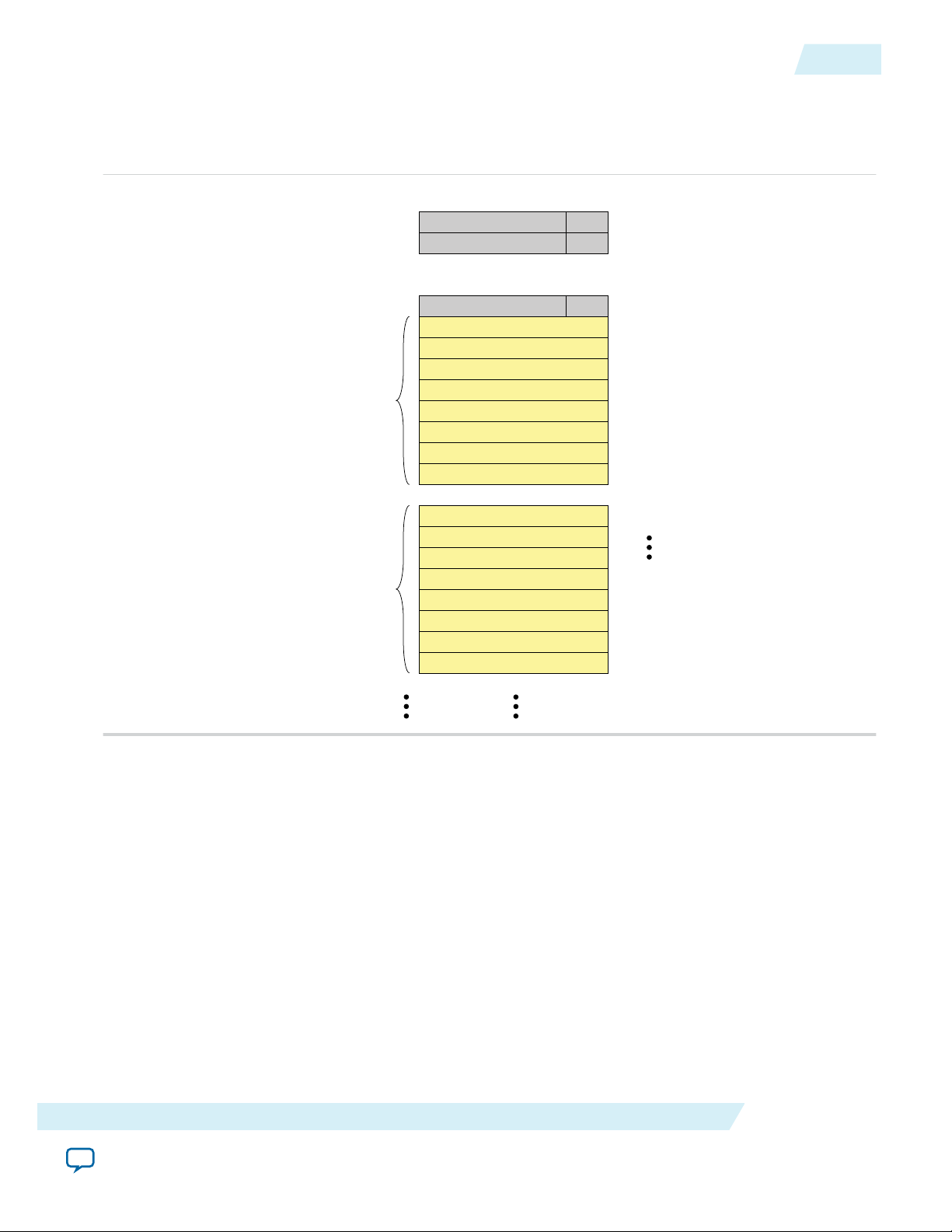
Reserved Done
0xF000_0000
0xF000_0200
0xF000_0204
0xF000_0208
0xF000_020C
0xF000_0210
Reserved Done
Reserved
Addresss
Done
SRC_ADDR_LOW
DESCRIPTOR_ID + DMA_LENGTH
SRC_ADDR_HIGH
DEST_ADDR_LOW
DEST_ADDR_HIGH
Descriptor 0
Descriptor 1
Descriptor 0 Status
Descriptor 1 Status
Descriptor 127 Status
127 0
Bits
RESERVED
RESERVED
RESERVED
UG-01154
2014.12.18
Read DMA Example
Figure 5-11: Descriptor Table Format
Assume the descriptor table includes 128 entries. The status table precedes a variable number of
descriptors in memory. The Read and Write Status and Descriptor Tables are at the address specified in
the RC Read Descriptor Base Register and RC Write Descriptor Base Register, respectively.
5-23
Registers
1. Calculate the memory allocation required:
a. Each descriptor is 32 bytes. The three descriptors require 96 bytes of memory
b. Each entry in the status table is 4 bytes. The 128 entries require 512 bytes of memory.
The total memory allocation for the status and descriptor tables is 608 bytes.
2. Allocate 608 bytes of memory.
Assume that the start address of the allocated memory is 0xF000_0000.
3. Create the descriptor table in the PCI Express address space. Because the status table is stored before
the descriptors, the first descriptor is stored at 0xF000_0000 + 0x200 = 0xF000_0200.
a. Program 0x1000_0000 to source address 0xF000_02004.
This is the upper 32 bits of the source address.
b. Program 0x0000_0000 to source address 0xF000_0200.
This is the lower 32 bits of the source address.
c. Program 0x5000_0000 to destination address 0xF000_020C.
Altera Corporation
Send Feedback
Page 93

5-24
Read DMA Example
UG-01154
2014.12.18
This is the upper 32 bits of the destination address.
d. Program 0 to destination address 0xF000_0208.
This is the lower 32 bits of the destination address.
e. Program 0x0003_FFFF to 0xF000_0210 to transfer 1 MByte of data for descriptor ID 0.
4. Repeat this procedure for the second data block:
a. Program 0x2000_0000 to source address 0xF000_0224.
b. Program 0x0000_0000 to source address 0xF000_0220.
c. Program 0x0001_0000 to destination address 0xF000_022C.
d. Program 0x0000_0000 to destination address 0xF000_0228.
e. Program 0x0005_FFFF to 0xF000_0230 to transfer 512 KBytes of data for descriptor ID 1.
5. Repeat this procedure for the third data block:
a. Program 0x2000_0000 to source address 0xF000_024C.
b. Program 0x0000_0001 to source address 0xF000_0248.
c. Program 0x1000_0000 to destination address 0xF000_0254.
d. Program 0x0000_0000 to destination address 0xF000_0250.
e. Program 0x0005_FFFF to 0xF000_0250 to transfer 256 KBytes of data for descriptor ID 2.
6. Program the DMA Descriptor Controller with the address of the status and descriptor table in the PCI
Express address space. The Read DMA registers start at offset 0.
a. Program 0x0 to offset 0x4.
This is the upper 32 bits of the PCIe memory where the status and descriptor table is stored.
b. Program 0xF000_0000 to offset 0x0.
This is the lower 32 bits of the address in PCIe memory that stores the status and descriptor tables.
The Read DMA automatically adds an offset of 0x200 to this value to start the copy after the status
table.
7. Program the DMA Descriptor Controller with the on-chip FIFO address. This is the address to which
the Descriptor Controller will copy the status and descriptor table.
a. Program 0x0 to offset 0xC
This is the upper 32 bits of the on-chip FIFO address in the Avalon-MM address domain.
b. Program 0xc000_0000 to offset 0x8.
This is the lower 32 bits of the on-chip FIFO address. This is address of the internal on-chip FIFO
that is a part of the Descriptor Controller as seen by the RX Master.
8. Program the Descriptor Controller RD_DMA_LAST_PTR register.
This step starts the DMA. It also specifies the status dword to be updated when the three descriptors
complete.
Altera Corporation
• To update a single done bit for the final descriptor, program 0x2 to offset 0x10. The Descriptor
Controller processes all three descriptors and writes the done bit to 0xF000_0008 of the status table.
• To update the done bits for all three descriptors, program 0x10 three times with the values 0, 1, and
2. The Descriptor Controller sets the done bits for addresses 0xF000_0000, 0xF000_0004, and
0xF000_0008. If the system supports out-of-order Read Completions, the Descriptor Controller
may complete descriptors out of order. In such systems, you must use this method of requesting
done status for each descriptor. Software must check for done status for every descriptor.
Registers
Send Feedback
Page 94

UG-01154
2014.12.18
Software Program for Simultaneous Read and Write DMA
Software Program for Simultaneous Read and Write DMA
Program the following steps to implement a simultaneous DMA transfer:
1. Allocate Root Port memory for the Read and Write DMA descriptor tables. Assume the table includes
up to 128, eight-dword descriptors and 128, one-dword status entries for a total of 1152 dwords. Total
memory for the Read and Write DMA descriptor tables is 2304 dwords.
2. Allocate Root Port memory and initialize it with data for the Read DMA to read.
3. Allocate Root Port memory for the Write DMA to write.
4. Create all the descriptors for the read DMA descriptor table. Assign the DMA Descriptor IDs
sequentially, starting with 0 to a maximum of 127. For the read DMA, the source address is the
memory space allocated in Step 2. The destination address is the Avalon-MM address that the Read
DMA module writes. Specify the DMA length in dwords. Each descriptor transfers contiguous
memory. Assuming a base address of 0, for the Read DMA, the following assignments illustrate
construction of a read descriptor:
a. RD_RC_LOW_SRC_ADDR = 0x0000 (The base address for the read descriptor table in
the Root Port
b. RD_RC_HIGH_SRC_ADDR = 0x0004
c. RD_CTLR_LOW_DEST_ADDR 0x0008
d. RD_CTLR_HIGH_DEST_ADDR = 0x000C
e. RD_DMA_LAST_PTR = 0x0010
Writing the RD_DMA_LAST_PTR register starts operation.
5. For the Write DMA, the source address is the Avalon-MM address that the Write DMA module
should read. The destination address is the Root Port memory space allocated in Step 3. Specify the
DMA length in dwords. Assuming a base address of 0x100, for the Write DMA, the following
assignments illustrate construction of a write descriptor:
a. RD_RC_LOW_SRC_ADDR = 0x0100 (The base address for the read descriptor table in
the Root Port
b. WD_RC_HIGH_SRC_ADDR = 0x0104
c. WD_CTLR_LOW_DEST_ADDR 0x0108
d. WD_CTLR_HIGH_DEST_ADDR = 0x010C
e. WD_DMA_LAST_PTR = 0x0110
Writing the WD_DMA_LAST_PTR register starts operation.
6. To improve throughput, the Read DMA module copies the descriptor table to the Avalon-MM
memory before beginning operation. Specify the memory address by writing to the EP Descriptor
Table Base (Low) and (High) registers.
7. An MSI interrupt is sent for each WD_DMA_LAST_PTR or RD_DMA_LAST_PTR that completes. These
completions result in updates to the done status bits. Host software can then read status bits to
determine which DMA operations are complete.
5-25
Registers
Note:
Send Feedback
Out-of-order completions are supported for Read DMA requests. If the transfer size of the read
DMA is greater than the maximum read request size, the Read DMA creates multiple read
requests. For example, if Maximum Read Request Size is 512 bytes, the Read DMA breaks a
4 KByte read request into 8 requests with 8 different tags. The Read Completions can come back in
any order. The Read DMA Avalon-MM master port writes the Read Completions to the correct
locations, based on the tags.
Altera Corporation
Page 95

5-26
Control Register Access (CRA) Avalon-MM Slave Port
Control Register Access (CRA) Avalon-MM Slave Port
Table 5-19: Configuration Space Register Descriptions
The optional CRA Avalon-MM slave port provides host access to selected Configuration Space and status
registers. These registers are read only. For registers that are less than 32 bits, the upper bits are unused.
Byte Offset
Register Dir Description
UG-01154
2014.12.18
14'h0000 cfg_dev_ctrl[15:0]
14'h0004 cfg_dev_ctrl2[15:0]
14'h0008 cfg_link_ctrl[15:0]
14'h000C cfg_link_ctrl2[15:0]
O cfg_devctrl[15:0] is device control for the PCI
Express capability structure.
O cfg_dev2ctrl[15:0] is device control 2 for the
PCI Express capability structure.
O cfg_link_ctrl[15:0]is the primary Link Control
of the PCI Express capability structure.
For Gen2 or Gen3 operation, you must write a 1’b1
to Retrain Link bit (Bit[5] of the cfg_link_ctrl) of
the Root Port to initiate retraining to a higher data
rate after the initial link training to Gen1 L0 state.
Retraining directs the LTSSM to the Recovery state.
Retraining to a higher data rate is not automatic
even if both devices on the link are capable of a
higher data rate.
O cfg_link_ctrl2[31:16] is the secondary Link
Control register of the PCI Express capability
structure for Gen2 operation.
When tl_cfg_addr=2, tl_cfg_ctl returns the
primary and secondary Link Control registers,
{cfg_link_ctrl[15:0], cfg_link_
ctrl2[15:0]}, the primary Link Status register
contents is available on tl_cfg_sts[46:31].
14'h0010 cfg_prm_cmd[15:0]
14'h0014 cfg_root_ctrl[7:0]
Altera Corporation
For Gen1 variants, the link bandwidth notification
bit is always set to 0.For Gen2 variants, this bit is set
to 1.
O Base/Primary Command register for the PCI
Configuration Space.
O Root control and status register of the PCI-Express
capability. This register is only available in Root
Port mode.
Registers
Send Feedback
Page 96

UG-01154
2014.12.18
Control Register Access (CRA) Avalon-MM Slave Port
5-27
Byte Offset
Register Dir Description
14'h0018 cfg_sec_ctrl[15:0]
14'h001C cfg_secbus[7:0]
14'h0020 cfg_subbus[7:0]
14'h0024 cfg_msi_addr_low[31:0]
14'h0028 cfg_msi_addr_hi[63:32]
14'h002C cfg_io_bas[19:0]
14'h0030 cfg_io_lim[19:0]
O Secondary bus Control and Status register of the
PCI-Express capability. This register is only
available in Root Port mode.
O Secondary bus number. Available in Root Port
mode.
O Subordinate bus number. Available in Root Port
mode.
O cfg_msi_add[31:0] is the MSI message address.
O cfg_msi_add[63:32] is the MSI upper message
address.
O The IO base register of the Type1 Configuration
Space. This register is only available in Root Port
mode.
O The IO limit register of the Type1 Configuration
Space. This register is only available in Root Port
mode.
14'h0034 cfg_np_bas[11:0]
14'h0038 cfg_np_lim[11:0]
14'h003C cfg_pr_bas_low[31:0]
14'h0040 cfg_pr_bas_hi[43:32]
14'h0044 cfg_pr_lim_low[31:0]
O The non-prefetchable memory base register of the
Type1 Configuration Space. This register is only
available in Root Port mode.
O The non-prefetchable memory limit register of the
Type1 Configuration Space. This register is only
available in Root Port mode.
O The lower 32 bits of the prefetchable base register of
the Type1 Configuration Space. This register is only
available in Root Port mode.
O The upper 12 bits of the prefetchable base registers
of the Type1 Configuration Space. This register is
only available in Root Port mode.
O The lower 32 bits of the prefetchable limit registers
of the Type1 Configuration Space. This register is
only available in Root Port mode.
Registers
Altera Corporation
Send Feedback
Page 97

5-28
Control Register Access (CRA) Avalon-MM Slave Port
UG-01154
2014.12.18
Byte Offset
Register Dir Description
14'h0048 cfg_pr_lim_hi[43:32]
14'h004C cfg_pmcsr[31:0]
14'h0050 cfg_msixcsr[15:0]
14'h0054 cfg_msicsr[15:0]
14'h0058 cfg_tcvcmap[23:0]
O The upper 12 bits of the prefetchable limit registers
of the Type1 Configuration Space. This register is
only available in Root Port mode.
O cfg_pmcsr[31:16] is Power Management Control
and cfg_pmcsr[15:0]is the Power Management
Status register.
O MSI-X message control register.
O MSI message control.
O Configuration traffic class (TC)/virtual channel
(VC) mapping. The Application Layer uses this
signal to generate a TLP mapped to the appropriate
channel based on the traffic class of the packet.
The following encodings are defined:
• cfg_tcvcmap[2:0]: Mapping for TC0 (always 0)
.
• cfg_tcvcmap[5:3]: Mapping for TC1.
• cfg_tcvcmap[8:6]: Mapping for TC2.
• cfg_tcvcmap[11:9]: Mapping for TC3.
• cfg_tcvcmap[14:12]: Mapping for TC4.
• cfg_tcvcmap[17:15]: Mapping for TC5.
• cfg_tcvcmap[20:18]: Mapping for TC6.
• cfg_tcvcmap[23:21]: Mapping for TC7.
14'h005C cfg_msi_data[15:0]
14'h0060 cfg_busdev[12:0]
Altera Corporation
O cfg_msi_data[15:0] is message data for MSI.
O Bus/Device Number captured by or programmed in
the Hard IP.
Registers
Send Feedback
Page 98

UG-01154
2014.12.18
Control Register Access (CRA) Avalon-MM Slave Port
5-29
Byte Offset
Register Dir Description
14'h0064 ltssm_reg[4:0]
Specifies the current LTSSM state. The LTSSM state
O
machine encoding defines the following states: :
• 5'b: 00000: Detect.Quiet
• 5'b: 00001: Detect.Active
• 5'b: 00010: Polling.Active
• 5'b: 00011: Polling.Compliance
• 5'b: 00100: Polling.Configuration
• 5'b: 00101: Polling.Speed
• 5'b: 00110: config.Linkwidthstart
• 5'b: 00111: Config.Linkaccept
• 5'b: 01000: Config.Lanenumaccept
• 5'b: 01001: Config.Lanenumwait
• 5'b: 01010: Config.Complete
• 5'b: 01011: Config.Idle
• 5'b: 01100: Recovery.Rcvlock
• 5'b: 01101: Recovery.Rcvconfig
• 5'b: 01110: Recovery.Idle
• 5'b: 01111: L0
• 5'b: 10000: Disable
• 5'b: 10001: Loopback.Entry
• 5'b: 10010: Loopback.Active
• 5'b: 10011: Loopback.Exit
• 5'b: 10100: Hot.Reset
• 5'b: 10101: LOs
• 5'b: 11001: L2.transmit.Wake
• 5'b: 11010: Speed.Recovery
• 5'b: 11011: Recovery.Equalization, Phase 0
• 5'b: 11100: Recovery.Equalization, Phase 1
• 5'b: 11101: Recovery.Equalization, Phase 2
• 5'b: 11110: recovery.Equalization, Phase 3
Registers
14'h0068
Send Feedback
current_speed_reg[1:0]
O Indicates the current speed of the PCIe link. The
following encodings are defined:
• 2b’00: Undefined
• 2b’01: Gen1
• 2b’10: Gen2
• 2b’11: Gen3
Altera Corporation
Page 99

5-30
Control Register Access (CRA) Avalon-MM Slave Port
UG-01154
2014.12.18
Byte Offset
Register Dir Description
14'h006C lane_act_reg[3:0]
Related Information
• PCI Express Base Specification 2.1 or 3.0
• PCI Local Bus Specification, Rev. 3.0
O Lane Active Mode: This signal indicates the number
of lanes that configured during link training. The
following encodings are defined:
• 4’b0001: 1 lane
• 4’b0010: 2 lanes
• 4’b0100: 4 lanes
• 4’b1000: 8 lanes
Altera Corporation
Registers
Send Feedback
Page 100

2014.12.18
www.altera.com
101 Innovation Drive, San Jose, CA 95134
Reset and Clocks
6
UG-01154
Subscribe
Send Feedback
V-Series Hard IP for PCI Express IP Core includes both a soft reset controller and a hard reset controller.
Software selects the appropriate reset controller depending on the configuration you specify. Both reset
controllers reset the IP core and provide sample reset logic in the example design. The figure below
provides a simplified view of the logic that implements both reset controllers.
The pin_perst signal from the input pin of the FPGA resets the Hard IP for PCI Express IP Core.
app_rstn which resets the Application Layer logic is derived from reset_status and pld_clk_inuse,
which are outputs of the core. This reset controller is implemented in hardened logic. The figure below
provides a simplified view of the logic that implements the reset controller.
Table 6-1: Use of Hard and Soft Reset Controllers
Reset Controller Used Description
Hard Reset Controller pin_perst from the input pin of the FPGA resets the Hard IP for PCI Express
IP Core. app_rstn which resets the Application Layer logic is derived from
reset_status and pld_clk_inuse, which are outputs of the core. This reset
controller is supported for Gen 1 production devices.
Soft Reset Controller Either pin_perst from the input pin of the FPGA or npor which is derived
from pin_perst or local_rstn can reset the Hard IP for PCI Express IP
Core. Application Layer logic generates the optional local_rstn signal. app_
rstn which resets the Application Layer logic is derived from npor.
©
2014 Altera Corporation. All rights reserved. ALTERA, ARRIA, CYCLONE, ENPIRION, MAX, MEGACORE, NIOS, QUARTUS and STRATIX words and logos are
trademarks of Altera Corporation and registered in the U.S. Patent and Trademark Office and in other countries. All other words and logos identified as
trademarks or service marks are the property of their respective holders as described at www.altera.com/common/legal.html. Altera warrants performance
of its semiconductor products to current specifications in accordance with Altera's standard warranty, but reserves the right to make changes to any
products and services at any time without notice. Altera assumes no responsibility or liability arising out of the application or use of any information,
product, or service described herein except as expressly agreed to in writing by Altera. Altera customers are advised to obtain the latest version of device
specifications before relying on any published information and before placing orders for products or services.
This reset controller is supported for Gen2 and Gen3 production devices.
ISO
9001:2008
Registered
 Loading...