

Page 1

Viterbi IP Core User Guide
Subscribe
Send Feedback
UG-VITERBI
2014.12.15
101 Innovation Drive
San Jose, CA 95134
www.altera.com
Page 2

TOC-2
Contents
About the Viterbi IP Core...................................................................................1-1
Viterbi IP Core Getting Started..........................................................................2-1
Altera DSP IP Core Features...................................................................................................................... 1-1
Viterbi II IP Core Features......................................................................................................................... 1-1
DSP IP Core Device Family Support.........................................................................................................1-2
DSP IP Core Verification............................................................................................................................1-2
Viterbi IP Core Release Information.........................................................................................................1-2
Viterbi IP Core Performance and Resource Utilization.........................................................................1-3
Installing and Licensing IP Cores..............................................................................................................2-1
OpenCore Plus IP Evaluation........................................................................................................ 2-1
Viterbi IP Core OpenCore Plus Timeout Behavior.................................................................... 2-2
IP Catalog and Parameter Editor...............................................................................................................2-2
Specifying IP Core Parameters and Options............................................................................................2-3
Files Generated for Altera IP Cores...............................................................................................2-4
Simulating Altera IP Cores in other EDA Tools..................................................................................... 2-7
DSP Builder Design Flow............................................................................................................................2-8
Viterbi IP Core Functional Description.............................................................3-1
Decoder......................................................................................................................................................... 3-1
Convolutional Encoder...............................................................................................................................3-1
Trellis Coded Modulation...........................................................................................................................3-2
Half-Rate Convolutional Codes.....................................................................................................3-2
Trellis Decoder.................................................................................................................................3-4
About Converting Received Signals..............................................................................................3-5
Trellis Termination..........................................................................................................................3-7
Trellis Initialization .........................................................................................................................3-7
Viterbi IP Core Parameters........................................................................................................................ 3-7
Architecture......................................................................................................................................3-7
Code Sets...........................................................................................................................................3-9
Viterbi Parameters.........................................................................................................................3-10
Test Data......................................................................................................................................... 3-12
Viterbi IP Core Interfaces and Signals....................................................................................................3-14
Avalon-ST Interfaces in DSP IP Cores....................................................................................... 3-14
Global Signals.................................................................................................................................3-14
Avalon-ST Sink Signals.................................................................................................................3-14
Avalon Source-ST Signals.............................................................................................................3-16
Configuration Signals....................................................................................................................3-17
Status Signals.................................................................................................................................. 3-18
Viterbi IP Core Timing Diagrams...............................................................................................3-18
Altera Corporation
Page 3

TOC-3
Document Revision History................................................................................4-1
Altera Corporation
Page 4

2014.12.15
www.altera.com
101 Innovation Drive, San Jose, CA 95134
About the Viterbi IP Core
1
UG-VITERBI
Subscribe
Altera DSP IP Core Features
• Avalon® Streaming (Avalon-ST) interfaces
• DSP Builder ready
• Testbenches to verify the IP core
• IP functional simulation models for use in Altera-supported VHDL and Verilog HDL simulators
Viterbi II IP Core Features
• High-speed parallel architecture:
• Performance of over 250 megabits per second (Mbps)
• Fully parallel operation
• Optimized block decoding and continuous decoding
• Low to medium-speed, hybrid architecture:
Send Feedback
• Configurable number of add compare and select (ACS) units
• Memory-based architecture
• Wide range of performance; wide range of logic area
• Fully parameterized Viterbi decoder, including:
• Number of coded bits
• Constraint length
• Number of soft bits
• Traceback length
• Polynomial for each coded bit
• Variable constraint length
• Trellis coded modulation (TCM) option
©
2015 Altera Corporation. All rights reserved. ALTERA, ARRIA, CYCLONE, ENPIRION, MAX, MEGACORE, NIOS, QUARTUS and STRATIX words and logos are
trademarks of Altera Corporation and registered in the U.S. Patent and Trademark Office and in other countries. All other words and logos identified as
trademarks or service marks are the property of their respective holders as described at www.altera.com/common/legal.html. Altera warrants performance
of its semiconductor products to current specifications in accordance with Altera's standard warranty, but reserves the right to make changes to any
products and services at any time without notice. Altera assumes no responsibility or liability arising out of the application or use of any information,
product, or service described herein except as expressly agreed to in writing by Altera. Altera customers are advised to obtain the latest version of device
specifications before relying on any published information and before placing orders for products or services.
ISO
9001:2008
Registered
Page 5

1-2
DSP IP Core Device Family Support
DSP IP Core Device Family Support
Altera® offers the following device support levels for Altera IP cores:
• Preliminary support—Altera verifies the IP core with preliminary timing models for this device family.
The IP core meets all functional requirements, but might still be undergoing timing analysis for the
device family. You can use it in production designs with caution.
• Final support—Altera verifies the IP core with final timing models for this device family. The IP core
meets all functional and timing requirements for the device family. You can use it in production
designs.
Table 1-1: DSP IP Core Device Family Support
Device Family Support
Arria® II GX Final
Arria II GZ Final
Arria V Final
Arria 10 Final
UG-VITERBI
2014.12.15
Cyclone® IV Final
Cyclone V Final
MAX® 10 FPGA Final
Stratix® IV GT Final
Stratix IV GX/E Final
Stratix V Final
Other device families No support
DSP IP Core Verification
Before releasing a version of an IP core, Altera runs comprehensive regression tests to verify its quality
and correctness. Altera generates custom variations of the IP core to exercise the various parameter
options and thoroughly simulates the resulting simulation models with the results verified against master
simulation models.
Viterbi IP Core Release Information
Use the release information when licensing the IP core.
Table 1-2: Release Information
Version 14.1
Altera Corporation
Item Description
About the Viterbi IP Core
Send Feedback
Page 6

UG-VITERBI
2014.12.15
Item Description
Viterbi IP Core Performance and Resource Utilization
Release Date December 2014
Ordering Code IP-VITERBI/HS (parallel architecture) IP-VITERBI/SS (hybrid
Product ID 0037 (parallel architecture) 0038 (hybrid architecture)
Vendor ID 6AF7
Altera verifies that the current version of the Quartus II software compiles the previous version of each IP
core. Altera does not verify that the Quartus II software compiles IP core versions older than the previous
version. The Altera IP Release Notes lists any exceptions.
Related Information
• Altera IP Release Notes
• Errata for Viterbi IP core in the Knowledge Base
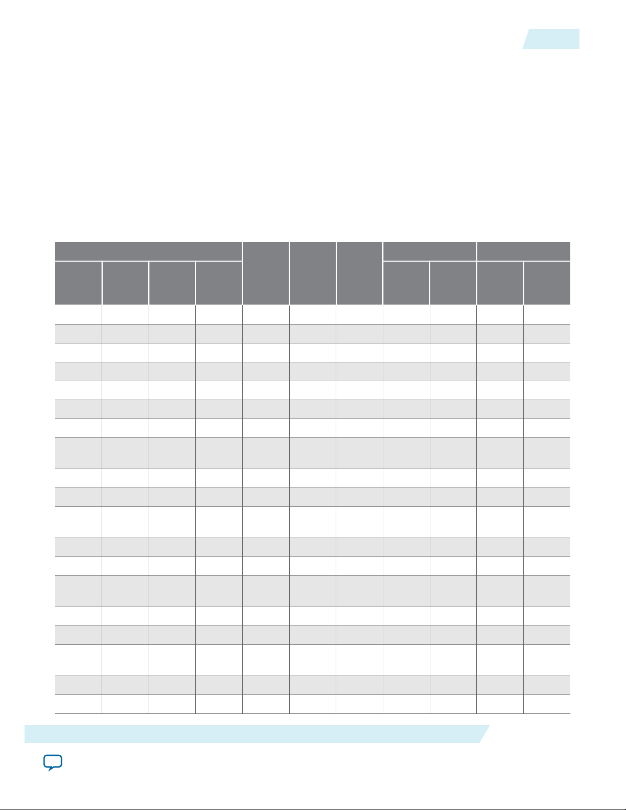
Viterbi IP Core Performance and Resource Utilization
This typical expected performance uses different architectures and constraint length, L, combinations,
and ACS units, A, and the Quartus II software. Performance largely depends on constraint length, L.
1-3
architecture)
Hybrid Architecture
The typical expected performance for a hybrid Viterbi IP core uses the Quartus II software with the Arria
V (5AGXFB3H4F40C4), Cyclone V (5CGXFC7D6F31C6), and Stratix V (5SGSMD4H2F35C2) devices
and the following parameters:
• v = 6 × L
• softbits = 3
• N = 2
where:
• v is the traceback length
• L is the constraint length
• N is the number of coded bits
• A is the number of ACS units
Table 1-3: Typical Performance
Parameters
L A M10K M20K Primary Secondary
Device ALM f
MAX
(MHz)
Memory Registers
5 1 Arria 10 401 383 -- 3 422 40
5 1 Arria V 323 201 5 -- 390 60
5 1 Cyclone V 324 172 5 -- 390 53
5 1 Stratix V 316 432 -- 5 388 44
7 1 Arria 10 521 370 -- 4 559 50
About the Viterbi IP Core
Send Feedback
Altera Corporation
Page 7

1-4
Viterbi IP Core Performance and Resource Utilization
UG-VITERBI
2014.12.15
Parameters
L A M10K M20K Primary Secondary
Device ALM f
MAX
(MHz)
Memory Registers
7 1 Arria V 427 207 6 -- 507 58
7 1 Cyclone V 427 185 6 -- 507 74
7 1 Stratix V 417 438 -- 6 506 51
7 2 Arria 10 622 363 -- 4 670 51
7 2 Arria V 529 215 6 -- 625 71
7 2 Cyclone V 532 180 6 -- 625 74
7 2 Stratix V 502 408 -- 6 625 56
7 4 Arria 10 835 366 -- 4 885 101
7 4 Arria V 744 204 6 -- 856 99
7 4 Cyclone V 746 173 6 -- 856 100
7 4 Stratix V 652 382 -- 6 856 82
9 1 Arria 10 932 343 -- 9 970 88
1 Arria V 792 190 11 -- 927 90
9 1 Cyclone V 794 176 11 -- 926 96
9 1 Stratix V 777 393 -- 11 924 94
9 16 Arria V 2,118 188 17 -- 2,743 309
9 16 Cyclone V 2,119 163 17 -- 2,744 275
9 16 Stratix V 1,887 348 -- 17 2,738 198
9 2 Arria 10 1,029 363 -- 9 1,091 74
9 2 Arria V 889 205 11 -- 1,053 98
9 2 Cyclone V 889 180 11 -- 1,053 96
9 2 Stratix V 883 377 -- 11 1,053 115
9 4 Arria 10 1,240 298 -- 9 1,321 87
9 4 Arria V 1,097 201 11 -- 1,302 137
9 4 Cyclone V 1,096 159 11 -- 1,302 126
9 4 Stratix V 1,021 390 -- 11 1,302 119
9 8 Arria V 1,465 197 13 -- 1,788 193
9 8 Cyclone V 1,465 163 13 -- 1,789 191
9 8 Stratix V 1,398 351 -- 13 1,790 154
Altera Corporation
About the Viterbi IP Core
Send Feedback
Page 8
UG-VITERBI
2014.12.15
Parallel Architecture
The typical expected performance for a parallel Viterbi IP core uses the Quartus II software with the Arria
V (5AGXFB3H4F40C4), Cyclone V (5CGXFC7D6F31C6), and Stratix V (5SGSMD4H2F35C2) devices.
The following parameters apply:
• v = 6 ×L
• N = 2
where:
• v is the traceback length
• L is the constraint length
• N is the number of coded bits
Table 1-4: Typical Performance
Viterbi IP Core Performance and Resource Utilization
1-5
Parameters
softbits L Optimiz
ation
Best
State
Finder
Device ALMs
fMAX
(MHz)
Memory Registers
M10K M20K Primary Seconda
5 3 — On Arria 10 420 400 -- 5 500 63
7 3 — On Arria 10 453 351 -- 5 534 75
3 3 — Off Arria 10 396 423 -- 5 473 39
5 3 — Off Arria 10 420 400 -- 5 500 63
7 3 — Off Arria 10 453 351 -- 5 534 75
3 7 Block Off Arria 10 1,454 354 -- 3 817 154
3 7 Block Off Arria V 1,537 201 5 -- 1,166 168
3 7 Block Off CycloneV1,544 149 5 -- 1,167 88
3 7 Block Off Stratix V 1,521 352 -- 3 1,167 154
3 3 — Off Arria V 378 237 5 -- 456 67
3 3 — Off CycloneV378 200 5 -- 456 84
3 3 — Off Stratix V 378 405 -- 5 455 45
ry
5 3 — Off Arria V 397 210 5 -- 483 68
5 3 — Off CycloneV397 188 5 -- 484 81
5 3 — Off Stratix V 396 406 -- 5 482 92
3 3 — On Arria V 378 237 5 -- 456 67
3 3 — On CycloneV378 200 5 -- 456 84
3 3 — On Stratix V 378 405 -- 5 455 45
5 3 — On Arria V 397 210 5 -- 483 68
About the Viterbi IP Core
Send Feedback
Altera Corporation
Page 9

1-6
Viterbi IP Core Performance and Resource Utilization
UG-VITERBI
2014.12.15
Parameters
softbits L Optimiz
ation
Best
State
Finder
Device ALMs
fMAX
(MHz)
Memory Registers
M10K M20K Primary Seconda
5 3 — On CycloneV397 188 5 -- 484 81
5 3 — On Stratix V 396 406 -- 5 482 92
7 3 — On Arria V 424 219 5 -- 518 82
7 3 — On CycloneV424 185 5 -- 519 76
7 3 — On Stratix V 424 408 -- 5 517 69
7 3 — Off Arria V 424 219 5 -- 518 82
7 3 — Off CycloneV424 185 5 -- 519 76
7 3 — Off Stratix V 424 408 -- 5 517 69
7 4 — Off Arria V 424 219 5 -- 518 82
7 4 — Off CycloneV424 185 5 -- 519 76
ry
7 4 — Off Stratix V 424 408 -- 5 517 69
3 7 Continu
Off Arria 10 1,180 365 -- 5 829 178
ous
3 7 Continu
Off Arria V 1,222 187 9 -- 1,137 250
ous
3 7 Continu
Off CycloneV1,223 157 9 -- 1,137 187
ous
3 7 Continu
Off Stratix V 1,220 325 -- 5 1,137 168
ous
Altera Corporation
About the Viterbi IP Core
Send Feedback
Page 10

2014.12.15
acds
quartus - Contains the Quartus II software
ip - Contains the Altera IP Library and third-party IP cores
altera - Contains the Altera IP Library source code
<IP core name> - Contains the IP core source files
www.altera.com
101 Innovation Drive, San Jose, CA 95134
Viterbi IP Core Getting Started
2
UG-VITERBI
Subscribe
Send Feedback
1.
Installing and Licensing IP Cores
The Altera IP Library provides many useful IP core functions for your production use without purchasing
an additional license. Some Altera MegaCore® IP functions require that you purchase a separate license
for production use. However, the OpenCore® feature allows evaluation of any Altera IP core in simulation
and compilation in the Quartus® II software. After you are satisfied with functionality and perfformance,
visit the Self Service Licensing Center to obtain a license number for any Altera product.
Figure 2-1: IP Core Installation Path
Note:
The default IP installation directory on Windows is <drive>:\altera\<version number>; on Linux it is
<home directory>/altera/ <version number>.
Related Information
• Altera Licensing Site
• Altera Software Installation and Licensing Manual
OpenCore Plus IP Evaluation
Altera's free OpenCore Plus feature allows you to evaluate licensed MegaCore IP cores in simulation and
hardware before purchase. You need only purchase a license for MegaCore IP cores if you decide to take
your design to production. OpenCore Plus supports the following evaluations:
©
2015 Altera Corporation. All rights reserved. ALTERA, ARRIA, CYCLONE, ENPIRION, MAX, MEGACORE, NIOS, QUARTUS and STRATIX words and logos are
trademarks of Altera Corporation and registered in the U.S. Patent and Trademark Office and in other countries. All other words and logos identified as
trademarks or service marks are the property of their respective holders as described at www.altera.com/common/legal.html. Altera warrants performance
of its semiconductor products to current specifications in accordance with Altera's standard warranty, but reserves the right to make changes to any
products and services at any time without notice. Altera assumes no responsibility or liability arising out of the application or use of any information,
product, or service described herein except as expressly agreed to in writing by Altera. Altera customers are advised to obtain the latest version of device
specifications before relying on any published information and before placing orders for products or services.
ISO
9001:2008
Registered
Page 11

2-2
Viterbi IP Core OpenCore Plus Timeout Behavior
• Simulate the behavior of a licensed IP core in your system.
• Verify the functionality, size, and speed of the IP core quickly and easily.
• Generate time-limited device programming files for designs that include IP cores.
• Program a device with your IP core and verify your design in hardware.
OpenCore Plus evaluation supports the following two operation modes:
• Untethered—run the design containing the licensed IP for a limited time.
• Tethered—run the design containing the licensed IP for a longer time or indefinitely. This requires a
connection between your board and the host computer.
Note: All IP cores that use OpenCore Plus time out simultaneously when any IP core in the design times
out.
Viterbi IP Core OpenCore Plus Timeout Behavior
All IP cores in a device time out simultaneously when the most restrictive evaluation time is reached. If
there is more than one IP core in a design, the time-out behavior of the other IP cores may mask the timeout behavior of a specific IP core .
For IP cores, the untethered time-out is 1 hour; the tethered time-out value is indefinite. Your design
stops working after the hardware evaluation time expires. The Quartus II software uses OpenCore Plus
Files (.ocp) in your project directory to identify your use of the OpenCore Plus evaluation program. After
you activate the feature, do not delete these files..
UG-VITERBI
2014.12.15
When the evaluation time expires the decbit signal goes low .
Related Information
• AN 320: OpenCore Plus Evaluation of Megafunctions
IP Catalog and Parameter Editor
The Quartus II IP Catalog (Tools > IP Catalog) and parameter editor help you easily customize and
integrate IP cores into your project. You can use the IP Catalog and parameter editor to select, customize,
and generate files representing your custom IP variation.
Note:
The IP Catalog (Tools > IP Catalog) and parameter editor replace the MegaWizard™ Plug-In
Manager for IP selection and parameterization, beginning in Quartus II software version 14.0. Use
the IP Catalog and parameter editor to locate and paramaterize Altera IP cores.
The IP Catalog lists installed IP cores available for your design. Double-click any IP core to launch the
parameter editor and generate files representing your IP variation. The parameter editor prompts you to
specify an IP variation name, optional ports, and output file generation options. The parameter editor
generates a top-level Qsys system file (.qsys) or Quartus II IP file (.qip) representing the IP core in your
project. You can also parameterize an IP variation without an open project.
Use the following features to help you quickly locate and select an IP core:
• Filter IP Catalog to Show IP for active device family or Show IP for all device families. If you have no
project open, select the Device Family in IP Catalog.
• Type in the Search field to locate any full or partial IP core name in IP Catalog.
• Right-click an IP core name in IP Catalog to display details about supported devices, open the IP core's
installation folder, and view links to documentation.
• Click Search for Partner IP, to access partner IP information on the Altera website.
Altera Corporation
Viterbi IP Core Getting Started
Send Feedback
Page 12
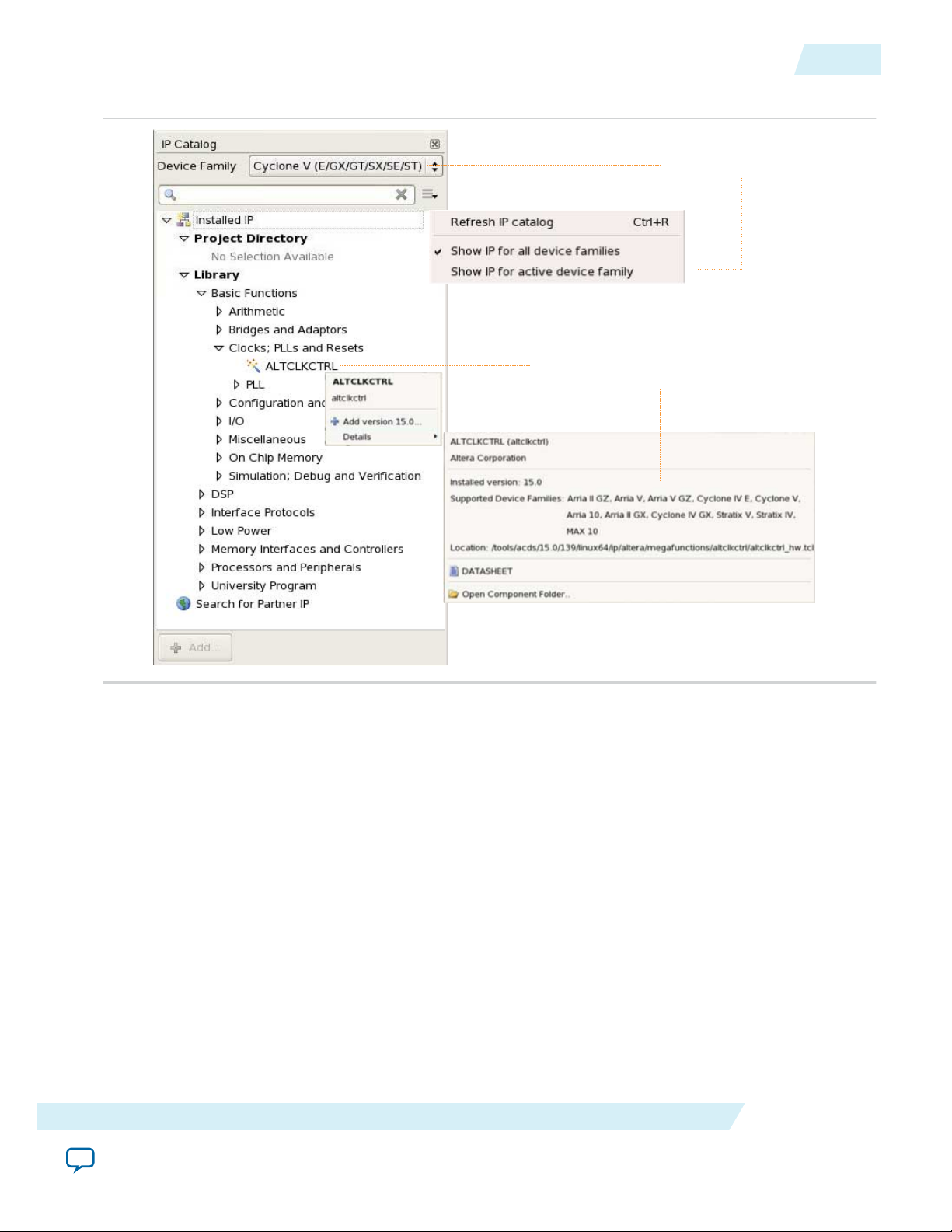
Search for installed IP cores
Double-click to customize, right-click for
detailed information
Show IP only for target device
UG-VITERBI
2014.12.15
Figure 2-2: Quartus II IP Catalog
Specifying IP Core Parameters and Options
2-3
Note: The IP Catalog is also available in Qsys (View > IP Catalog). The Qsys IP Catalog includes
exclusive system interconnect, video and image processing, and other system-level IP that are not
available in the Quartus II IP Catalog. For more information about using the Qsys IP Catalog, refer
to Creating a System with Qsys in the Quartus II Handbook.
Specifying IP Core Parameters and Options
You can quickly configure a custom IP variation in the parameter editor. Use the following steps to
specify IP core options and parameters in the parameter editor. Refer to Specifying IP Core Parameters
and Options (Legacy Parameter Editors) for configuration of IP cores using the legacy parameter editor.
1. In the IP Catalog (Tools > IP Catalog), locate and double-click the name of the IP core to customize.
The parameter editor appears.
2. Specify a top-level name for your custom IP variation. The parameter editor saves the IP variation
settings in a file named <your_ip>.qsys. Click OK.
3. Specify the parameters and options for your IP variation in the parameter editor, including one or
more of the following. Refer to your IP core user guide for information about specific IP core
parameters.
Viterbi IP Core Getting Started
Send Feedback
Altera Corporation
Page 13

View IP port
and parameter
details
Apply preset parameters for
specific applications
Specify your IP variation name
and target device
2-4
Files Generated for Altera IP Cores
• Optionally select preset parameter values if provided for your IP core. Presets specify initial
parameter values for specific applications.
• Specify parameters defining the IP core functionality, port configurations, and device-specific
features.
• Specify options for processing the IP core files in other EDA tools.
4. Click Generate HDL, the Generation dialog box appears.
5. Specify output file generation options, and then click Generate. The IP variation files generate
according to your specifications.
6. To generate a simulation testbench, click Generate > Generate Testbench System.
7. To generate an HDL instantiation template that you can copy and paste into your text editor, click
Generate > HDL Example.
8. Click Finish. The parameter editor adds the top-level .qsys file to the current project automatically. If
you are prompted to manually add the .qsys file to the project, click Project > Add/Remove Files in
Project to add the file.
9. After generating and instantiating your IP variation, make appropriate pin assignments to connect
ports.
Figure 2-3: IP Parameter Editor
UG-VITERBI
2014.12.15
Files Generated for Altera IP Cores
The Quartus II software generates the following IP core output file structure:
Altera Corporation
Viterbi IP Core Getting Started
Send Feedback
Page 14

<your_testbench>_tb.csv
<your_testbench>_tb.spd
<your_ip>.cmp - VHDL component declaration file
<your_ip>.ppf - XML I/O pin information file
<your_ip>.qip - Lists IP synthesis files
<your_ip>.sip - Contains assingments for IP simulation files
<your_ip>.v or .vhd
Top-level IP synthesis file
<your_ip>.v or .vhd
Top-level simulation file
<simulator_setup_scripts>
<your_ip>.qsys - System or IP integration file
<your_ip>_bb.v - Verilog HDL black box EDA synthesis file
<your_ip>_inst.v or .vhd - Sample instantiation template
<your_ip>_generation.rpt - IP generation report
<your_ip>.debuginfo - Contains post-generation information
<your_ip>.html - Connection and memory map data
<your_ip>.bsf - Block symbol schematic
<your_ip>.spd - Combines simulation scripts for multiple cores
<your_ip>_tb.qsys
Testbench system file
<your_ip>.sopcinfo - Software tool-chain integration file
<project directory>
<EDA tool setup
scripts>
<your_ip>
IP variation files
<testbench>_tb
testbench system
sim
Simulation files
synth
IP synthesis files
sim
simulation files
<EDA tool name>
Simulator scripts
<testbench>_tb
<ip subcores> n
Subcore libraries
sim
Subcore
Simulation files
synth
Subcore
synthesis files
<HDL files>
<HDL files>
<your_ip> n
IP variation files
testbench files
UG-VITERBI
2014.12.15
Figure 2-4: IP Core Generated Files
Files Generated for Altera IP Cores
2-5
Table 2-1: IP Core Generated Files
<my_ip>.qsys
<system>.sopcinfo Describes the connections and IP component parameterizations in
Viterbi IP Core Getting Started
Send Feedback
File Name Description
The Qsys system or top-level IP variation file. <my_ip> is the name
that you give your IP variation.
your Qsys system. You can parse its contents to get requirements
when you develop software drivers for IP components.
Downstream tools such as the Nios II tool chain use this file.
The .sopcinfo file and the system.h file generated for the Nios II tool
chain include address map information for each slave relative to each
master that accesses the slave. Different masters may have a different
address map to access a particular slave component.
Altera Corporation
Page 15

2-6
Files Generated for Altera IP Cores
File Name Description
<my_ip>.cmp The VHDL Component Declaration (.cmp) file is a text file that
contains local generic and port definitions that you can use in VHDL
design files.
UG-VITERBI
2014.12.15
<my_ip>.html
A report that contains connection information, a memory map
showing the address of each slave with respect to each master to
which it is connected, and parameter assignments.
<my_ip>_generation.rpt IP or Qsys generation log file. A summary of the messages during IP
generation.
<my_ip>.debuginfo Contains post-generation information. Used to pass System Console
and Bus Analyzer Toolkit information about the Qsys interconnect.
The Bus Analysis Toolkit uses this file to identify debug components
in the Qsys interconnect.
<my_ip>.qip
Contains all the required information about the IP component to
integrate and compile the IP component in the Quartus II software.
<my_ip>.csv Contains information about the upgrade status of the IP component.
<my_ip>.bsf A Block Symbol File (.bsf) representation of the IP variation for use
in Quartus II Block Diagram Files (.bdf).
<my_ip>.spd
Required input file for ip-make-simscript to generate simulation
scripts for supported simulators. The .spd file contains a list of files
generated for simulation, along with information about memories
that you can initialize.
<my_ip>.ppf The Pin Planner File (.ppf) stores the port and node assignments for
IP components created for use with the Pin Planner.
<my_ip>_bb.v You can use the Verilog black-box (_bb.v) file as an empty module
declaration for use as a black box.
<my_ip>.sip Contains information required for NativeLink simulation of IP
components. You must add the .sip file to your Quartus project.
<my_ip>_inst.v or _inst.vhd HDL example instantiation template. You can copy and paste the
contents of this file into your HDL file to instantiate the IP variation.
<my_ip>.regmap If the IP contains register information, the .regmap file generates.
The .regmap file describes the register map information of master
and slave interfaces. This file complements the .sopcinfo file by
providing more detailed register information about the system. This
enables register display views and user customizable statistics in
System Console.
Altera Corporation
Viterbi IP Core Getting Started
Send Feedback
Page 16

UG-VITERBI
2014.12.15
Simulating Altera IP Cores in other EDA Tools
File Name Description
2-7
<my_ip>.svd
<my_ip>.v
or
<my_ip>.vhd
mentor/
aldec/
/synopsys/vcs
/synopsys/vcsmx
Allows HPS System Debug tools to view the register maps of
peripherals connected to HPS within a Qsys system.
During synthesis, the .svd files for slave interfaces visible to System
Console masters are stored in the .sof file in the debug section.
System Console reads this section, which Qsys can query for register
map information. For system slaves, Qsys can access the registers by
name.
HDL files that instantiate each submodule or child IP core for
synthesis or simulation.
Contains a ModelSim® script msim_setup.tcl to set up and run a
simulation.
Contains a Riviera-PRO script rivierapro_setup.tcl to setup and run a
simulation.
Contains a shell script vcs_setup.sh to set up and run a VCS
®
simulation.
Contains a shell script vcsmx_setup.sh and synopsys_ sim.setup file to
set up and run a VCS MX® simulation.
/cadence
Contains a shell script ncsim_setup.sh and other setup files to set up
and run an NCSIM simulation.
/submodules Contains HDL files for the IP core submodule.
<child IP cores>/ For each generated child IP core directory, Qsys generates /synth and /
sim sub-directories.
Simulating Altera IP Cores in other EDA Tools
The Quartus II software supports RTL and gate-level design simulation of Altera IP cores in supported
EDA simulators. Simulation involves setting up your simulator working environment, compiling
simulation model libraries, and running your simulation.
You can use the functional simulation model and the testbench or example design generated with your IP
core for simulation. The functional simulation model and testbench files are generated in a project
subdirectory. This directory may also include scripts to compile and run the testbench. For a complete list
of models or libraries required to simulate your IP core, refer to the scripts generated with the testbench.
You can use the Quartus II NativeLink feature to automatically generate simulation files and scripts.
NativeLink launches your preferred simulator from within the Quartus II software.
Viterbi IP Core Getting Started
Send Feedback
Altera Corporation
Page 17

Post-fit timing
simulation netlist
Post-fit timing
simulation (3)
Post-fit functional
simulation netlist
Post-fit functional
simulation
Analysis & Synthesis
Fitter
(place-and-route)
TimeQuest Timing Analyzer
Device Programmer
Quartus II
Design Flow
Gate-Level Simulation
Post-synthesis
functional
simulation
Post-synthesis functional
simulation netlist
(Optional) Post-fit
timing simulation
RTL Simulation
Design Entry
(HDL, Qsys, DSP Builder)
Altera Simulation
Models
EDA
Netlist
Writer
2-8
DSP Builder Design Flow
Figure 2-5: Simulation in Quartus II Design Flow
UG-VITERBI
2014.12.15
Note: Post-fit timing simulation is supported only for Stratix IV and Cyclone IV devices in the current
version of the Quartus II software. Altera IP supports a variety of simulation models, including
simulation-specific IP functional simulation models and encrypted RTL models, and plain text
RTL models. These are all cycle-accurate models. The models support fast functional simulation of
your IP core instance using industry-standard VHDL or Verilog HDL simulators. For some cores,
only the plain text RTL model is generated, and you can simulate that model. Use the simulation
models only for simulation and not for synthesis or any other purposes. Using these models for
synthesis creates a nonfunctional design.
Related Information
Simulating Altera Designs
DSP Builder Design Flow
DSP Builder shortens digital signal processing (DSP) design cycles by helping you create the hardware
representation of a DSP design in an algorithm-friendly development environment.
This IP core supports DSP Builder. Use the DSP Builder flow if you want to create a DSP Builder model
that includes an IP core variation; use IP Catalog if you want to create an IP core variation that you can
instantiate manually in your design. For more information about the DSP Builder flow, refer to the
Altera Corporation
Viterbi IP Core Getting Started
Send Feedback
Page 18

UG-VITERBI
2014.12.15
Related Information
Using MegaCore Functions chapter in the DSP Builder Handbook.
DSP Builder Design Flow
2-9
Viterbi IP Core Getting Started
Send Feedback
Altera Corporation
Page 19

2014.12.15
RR
Port
MSB
LSB
ga_xor
gb_xor
www.altera.com
101 Innovation Drive, San Jose, CA 95134
Viterbi IP Core Functional Description
3
UG-VITERBI
Subscribe
Decoder
The Viterbi decoder can be a continuous or block decoder.
The continuous decoder processes a number of symbols greater than the traceback length. When the
decoder traces back the number of bits (traceback length), it delivers output bits. This behavior changes
when you assert the end of packet (EOP) signal. The decoder then switches to block decoding, starting
traceback from the last symbol or state. The tr_init_state signal indicates the end state that starts the
traceback operation. For block decoding Altera recommends you indicate the end state of the tail bits
(usually zero) and set the tb_type signal to 1.
Convolutional Encoder
The viterbi IP core convolutional encoder.
Figure 3-1: Convolutional Encoder
L = 5, N = 2 and polynomials GA = 19 and GB = 29. GA in decimal is 19, which is equal to 10011 in
binary. The most significant bit of the binary representation is the connection at the input data bit; the
least significant bit (LSB) represents the connection at the end of the shift register chain. The XOR
function implements the modulo-2 adding operation
Send Feedback
©
2015 Altera Corporation. All rights reserved. ALTERA, ARRIA, CYCLONE, ENPIRION, MAX, MEGACORE, NIOS, QUARTUS and STRATIX words and logos are
trademarks of Altera Corporation and registered in the U.S. Patent and Trademark Office and in other countries. All other words and logos identified as
trademarks or service marks are the property of their respective holders as described at www.altera.com/common/legal.html. Altera warrants performance
of its semiconductor products to current specifications in accordance with Altera's standard warranty, but reserves the right to make changes to any
products and services at any time without notice. Altera assumes no responsibility or liability arising out of the application or use of any information,
product, or service described herein except as expressly agreed to in writing by Altera. Altera customers are advised to obtain the latest version of device
specifications before relying on any published information and before placing orders for products or services.
ISO
9001:2008
Registered
Page 20

Uncoded Bit
Input
c
2
c
0
GB
GA
c
1
3-2
Trellis Coded Modulation
Trellis Coded Modulation
Trellis coded modulation (TCM) combines modulation and encoding processes to achieve better
efficiency without increasing the bandwidth.
Bandwidth-constrained channels operate in the region R/W > 1, where R = data rate and W = bandwidth
available. For such channels, digital communication systems use bandwidth efficient multilevel phase
modulation. For example, phase shift keying (PSK), phase amplitude modulation (PAM), or quadrature
amplitude modulation (QAM).
When you apply TCM to a bandwidth-constrained channel, you see a performance gain without
expanding the signal bandwidth. An increase in the number of signal phases from four to eight requires
approximately 4dB in additional signal power to maintain the same error rate. Hence, if TCM is to
provide a benefit, the performance gain of the rate 2/3 code must overcome this 4dB penalty. If the
modulation is an integral part of the encoding process and is designed in conjunction with the code to
increase the minimum Euclidian distance between the pairs of coded signals, the loss from the expansion
of the signal set is easily overcome and significant coding gain is achieved with relatively simple codes.
Any bandwidth-constrained system benefits from this technique, for example, satellite modem systems.
The TCM Viterbi decoder only supports N = 2 (only mother code rates of 1/2).
UG-VITERBI
2014.12.15
Half-Rate Convolutional Codes
A 1/2 rate convolutional code encodes one information bit and leaves the second information bit
uncoded.
Figure 3-2: Half-Rate Convolutional Code
With an eight-point signal constellation (e.g. eight-PSK), the two bits select one of the four subsets in the
signal constellation. The remaining information bit selects one of the two points within each subset.
Altera Corporation
Viterbi IP Core Functional Description
Send Feedback
Page 21

011
001
000
110
111
101
100
010
0
1
2
3
4
5
6
7
UG-VITERBI
2014.12.15
Half-Rate Convolutional Codes
Figure 3-3: Mapping of Coded Bits and Sector Numbers
The specific mapping is not important. You can derive other mappings by permutating subsets in a way
that preserves the main property of increased minimum distance among the subsets. However, you can
create any other mapping, including symbol mappings for 8-PSK, 16-PSK and others.
If you create another mapping, you must correctly connect the branch metrics created outside the IP core
to the input ports and correctly configure the polynomials GA and GB for the trellis generation.
3-3
Viterbi IP Core Functional Description
Send Feedback
Altera Corporation
Page 22

00
01
10
11
101
001
110
010
000 = (c2 c1 c0)
011
111
111
011
100
000
100
001
101
010
110
3-4
Trellis Decoder
Figure 3-4: Four-State Trellis
The four-state trellis is the trellis for the 1/2 rate convolution encoder with the addition of parallel paths in
each transition to accommodate the uncoded bit c2. The decoder uses the coded bits (c1, c0) to select one
of the four subsets that contain two signal points each It uses the uncoded bit to select one of the two
signal points within each subset.
UG-VITERBI
2014.12.15
Altera Corporation
Trellis Decoder
The decoder processes an arriving symbol to obtain four branch metric values and a sector number. The
branch metrics enter the Viterbi decoder in trellis mode and it obtains the encoded bit.
The encoder re-encodes this bit stream and the decoder uses the output of this encoder with the sector
number information to retrieve the uncoded bit. The testbench implements all the logic. The wizard
generates the branch metric values and sector number values, so you need no logic to create these values.
The testbench reads the sector number when it needs it. It has no delay functionality nor rotation. The
wizard-created data introduces has no phase error so the phase is aligned. In a real system, you must
calculate the phase. For a TCM code the BER block does not produce a meaningful output (numerr),
because the BER block does not compute errors at the input for TCM codes.
Viterbi IP Core Functional Description
Send Feedback
Page 23

decdat0
Viterbi
Decoder
Trellis Mode
Rate 1/2
Convolutional
Encoder
Trellis
Output
Demapper
decdat1
Branch
Metric
Rotate
Delay
Sector
Number
ROM
(I, Q)
to
Branch
Metric
and
Sector
Number
Rotate
Sector
Number
I
Q
UG-VITERBI
2014.12.15
Figure 3-5: Implementation of the Viterbi Decoder as a Trellis Decoder
About Converting Received Signals
The Viterbi decoder calculates the distances to the nearest four symbol points as an unsigned number in
the range 0...00 to 1...11 (number of softbits).
About Converting Received Signals
3-5
Where the range is equal to the radius of the symbol map. The decoder works with accumulative metrics
(not Euclidean metrics), so the decoder inverts these distances (000 becomes 111; 001 becomes110).
Viterbi IP Core Functional Description
Send Feedback
Altera Corporation
Page 24

Branch Metric 1
Branch Metric 3
Branch Metric 2
Branch Metric 0
Received Symbol
011
001
000
110
111
101
100
010
2
3-6
About Converting Received Signals
Figure 3-6: Conversion of Received Symbol into Four Branch Metrics and a Sector Number
UG-VITERBI
2014.12.15
For example, consider a received symbol that lands in sector number 2 with the following distances to the
four nearest symbol map points:
• 1111
• 1101
• 1011
• 0001
Where the distance of the radius for 4 softbits is 1111. The distances are inverted to obtain the following
branch metrics:
• Branch metric 0 = 0000
• Branch metric 1 = 0010
• Branch metric 2 = 0100
• Branch metric 3 = 1110
The decoder uses the coded bits (c1, c0) to select the branch metric number, which it uses to decide where
to connect the branch metrics to the rr input of the Viterbi decoder. Branch metric 3 goes to the most
significant bits (MSB) of rr; branch metric 0 goes to the least significant bits (LSB) of rr.
Altera Corporation
Viterbi IP Core Functional Description
Send Feedback
Page 25

UG-VITERBI
2014.12.15
Trellis Termination
Block decoders must properly decode the last bits of the block and adapt to the convolutional encoder.
Tail-biting feeds the convolutional encoder with a block and terminates it with (L – 1) unknown bits
taken from the end of the block. Tail-biting sets the initial state of the convolutional encoder with the last
(L – 1) information bits. Tail-biting is decoded by replicating the block at the decoder or double feeding
the block into the decoder. By decoding in the middle point, the trellis is forced into the state that is both
the initial state and the end state. From the first decoding block, you can take the last half of the block;
from the second decoded block (or second pass through the decoder), you can obtain the first half of the
bits of the block.
Note: In tail-biting, the block size must be large enough to train the decoder, otherwise you may see BER
Alternatively, if you initialize the convolutional encoder to zero, the initial state of the trellis is zero. The
decoder knows the last (L – 1) bits to the convolutional encoder. They bring the convolutional encoder to
a known end state. The decoder then uses this information to set the end state of the trellis with
tr_init_state, which is derived from the last (L – 1) bits of the block in reverse order. For example, for a
block that ends in: ...000101 If L = 5 and the decoder knows the last (L – 1) = 4 bits, it sets tr_init_state
as 0101, which reversed and in binary is 1010, or 10 in decimal. The wizard generates tr_init_state as if
it knows the last (L – 1) bits of each block.
loss.
Trellis Termination
3-7
Trellis Initialization
The parallel decoder always starts its trellis from state zero for a new block.
However, the hybrid decoder allows you to set the initial state (usually zero) with bm_init_state. This
signal ranges from 0 to 2 (L – 1) – 1, which are the trellis states. The bm_init_value signal initializes the
state metric of the state indicated by bm_init_state. The decoder initializes all other states with zero. The
appropriate value for this port is approximately 2
1)
. Continuous decoders never reset the state metrics, which creates a possible difference if the same block
of data is sent several times. Initially, the decoder sets the state metrics so that the state metric for state 0 is
0, and all others infinity. For any subsequent blocks, the state metrics contain whatever they have when
the previous block ends.
Viterbi IP Core Parameters
Architecture
Table 3-1: Architecture Parameters
Parameter Value Description
(bmgwide – 2)
or any value between 2
(N + softbits)
to 2
(bmgwide –
Viterbi architecure Hybrid or Parallel Selects the hybrid or parallel
Viterbi IP Core Functional Description
Send Feedback
architecture.
Altera Corporation
Page 26

Viterbi
Decoder
Input Symbols
Delay
Compare
and Count
BER Output
(numerr)
Convolutional
Encoder
3-8
BER Estimator
Parameter Value Description
BER On or Off Specifies the BER estimator
option, refer to “BER Estimator”
on page 3–7.
Node Sync On or Off Specifies the node synchroniza‐
tion option (only available when
BER option is on).
Optimizations None, Continuous, or Block Specifies the optimization for the
parallel decoder. if you select
None you can turn on Best State
Finder. However, to use less
logic, turn off Best State Finder.
BER Estimator
The BER estimator option uses a re-encode and compare approach for estimating the number of errors in
the input data.
Figure 3-7: BER Block Diagram
UG-VITERBI
2014.12.15
In cases where the signal-to-noise ratio is sufficiently high to allow the decoder to decode an error-free
output, the BER estimation is very close to the actual channel BER. When the decoder is not decoding an
error-free output, the estimated BER is higher and more random than the actual channel BER, which
introduces a degree of uncertainty directly proportional to the output errors.
Note:
For a TCM code, the BER block does not produce a meaningful output (numerr) because the BER
block does not compute errors at the input for TCM codes.
Altera Corporation
Viterbi IP Core Functional Description
Send Feedback
Page 27

3.00 3.50 4.00 4.50 5.00
5.50 6.00
Signal-to-Noise Ratio
BER
Actual BER
Estimated BER
1.00e-03
1.00e-02
1.00e-01
state_node_sync
Barrel
Rotator
rr(1)
rr(2)
...
RR(1)
RR(2)
...
rr(N) RR(N)
UG-VITERBI
2014.12.15
Figure 3-8: Graph Comparing Actual BER with Estimated BER
Node Synchronization
3-9
Node Synchronization
If you are not using external synchronization, you may not know the order of your N bits. The node
synchronization option allows you to rotate the rr inputs until the decoder is in synchronization. To use
node synchronization, you observe the BER and keep changing state_node_sync to rotate the rr inputs
until you get the correct value for the BER.
Figure 3-9: Node Synchronization Block Diagram
The following equation represents node synchronization:
RR[i] = rr[((state_node_sync + i – 1) mod N) + 1]
where i is 1 to N.
Viterbi IP Core Functional Description
RR and rr are treated as an array of width N of busses softbits wide. The range of valid values for
state_node_sync is 0 to (N – 1).
Code Sets
Send Feedback
Altera Corporation
Page 28

3-10
Viterbi Parameters
Table 3-2: Code Sets Parameters
Parameter Value Description
UG-VITERBI
2014.12.15
Number of
Code Sets
1 to 8 The Viterbi IP core supports multiple code definitions. The multiple
code set option allows up to eight code sets, where a code set comprises
a code rate and associated generating polynomials.
Number of
coded bits.
(N)
2 to 7 (hybrid)
2 to 4 (parallel)
For every bit to be encoded, N bits are output. With the multiple code
set option there are up to 5 different N parameters, which can be in any
order. Valid only for Viterbi mode. For TCM mode only N = 2 is
supported
Constraint
length (L)
3 to 9 The constraint length. Defines the number of states in the convolu‐
tional encoder, where number of states = 2(L – 1). You can choose
different values of L for each code set.
Decimal or
Octal
– Decimal or octal base representation for the generator polynomials.
The design file representation is decimal, but you have the option of
entering in either decimal or octal base.
Mode V or T Viterbi (V) or TCM mode (T).
GA, GB, GC,
GD, GE, GF,
GG
– The generator polynomials. If you use the multiple code set option, the
wizard enters a different set of polynomials in the respective gi group.
The wizard provides default values that you can overwritte by any valid
polynomial. (The wizard does not check whether the entered values are
valid.) The parallel architecture uses only GA, GB, GC, and GD.
For multiple code sets, the first code definition corresponds to the first line and is selected with sel_code
input = 0; the second line is selected with sel_code = 1; the third with sel_code = 2 and so on. For each
code definition you can select N, the polynomials, the constraint length L, and the mode (Viterbi or
TCM). You can mix different constraint lengths with different TCM and Viterbi modes. The test data,
which the wizardr creates, tests each of the code definitions. You can see these tests in the simulation with
the testbench or if you look at the block_period_stim.txt file.
In hybrid mode, for constraint lengths of 3 and 4, the bitwidth of tr_init_state is 4, but the MegaCore
function ignores the redundant higher bits.
For multiple constraint lengths, some of the last decoded bits may be incorrect, becauset of the Viterbi
algorithm. To avoid this effect, give a lower BER, and reduce the probability of being on the wrong trellis
path, set Optimization to None and turn on Best State Finder.
Viterbi Parameters
Maximum constraint length
(L
)
MAX
Altera Corporation
Parameter Value Description
5 to 9 (hybrid)
The maximum constraint length
L
. .
MAX
3 to 9 (parallel)
Viterbi IP Core Functional Description
Send Feedback
Page 29

UG-VITERBI
2014.12.15
Soft Symbol Input
Parameter Value Description
3-11
ACS Units (A) 1, 2, 4, 8, or 16 The number of ACS units, which
adds a degree of parallelism
(hybrid architecture only). The
range of values available depends
upon the value of maximum
constraint length L
MAX
.
Traceback (v) 8 (minimum) The traceback length, which is
the number of stages in the trellis
that are traced back to obtain a
decoded bit. It is typically set to 6
× L for unpunctured codes, and
up to 15 × L for highly
punctured codes.
Softbits (softbits) 1 to 16 The number of soft decision bits
per symbol. When softbits is set
to 1 bit, the decoder acts as a
hard decision decoder, and still
allows for erased symbols to be
entered using the eras_sym
input.
Bmgwide – The precision of the state metric
accumulation. The parameter
editor selects and displays the
optimum value, which depends
on N
MAX
, L
MAX
and, softbits.
Soft Symbol Input
The number of soft decision bits per symbol, softbits, represent 2
input values represent received signal amplitudes. If the input is in log-likelihood format, a transforma‐
tion is required and you must use extra softbits to retain signal integrity. The decoder marks depunctured
values separately. The decoder allows a hard-decision input when softbits = 1.
Table 3-3: Soft Symbol Input Representation
softbits = 3
Soft Symbol Meaning
011 Strongest '0'
010 Strong '0'
001 Weak '0'
000 Weakest '0'
softbits – 1
soft 0s and 2
softbits – 1
soft 1s. The
111 Weakest '1'
110 Weak '1'
101 Strong '1'
Viterbi IP Core Functional Description
Send Feedback
Altera Corporation
Page 30

3-12
State Metrics
Soft Symbol Meaning
100 Strongest '1'
State Metrics
The Viterbi decoder state metrics are accumulative not Euclidean and are based on maximum metrics
rather than minimum metrics.
UG-VITERBI
2014.12.15
As the metrics grow, normalize them to avoid overflow. When a normalization occurs the decoder
subtracts 2
(bmgwide – 1)
value for the best path = (number of normalizations) × (2
the best path, the number of symbols processed, and the number of errors in the BER block indicate the
quality of the channel and whether you have a suitable value for softbits. The output bestadd indicates the
state that has the best metric.
Throughput Calculator
The throughput calculator uses the following equation:
Hybrid throughput = f
where:
• • Z = 10, if log2C = 3
• Z= 2log2C, if log2C > 3
• log2C = L
• L
MAX
MAX
is the maximum constraint length
• A is ACS units
• Parallel throughput = f
Latency Calculator
The latency calculator gives you an approximate indication of the latency of your Viterbi decoder.
from all metrics and increases the normalization register by +1. The total metric
MAX
(bmgwide – 1)
/Z
) + bestmet. The total metric value for
– 2 – log2A
MAX
Latency is the number of clock cycles it takes the decoder to process r the data and output it. Latency is
from the first symbol to enter the IP core (sink_sop) up to the first symbol to leave (source_sop). The
latency depends on the parameters. For the precise latency, perform simulation. The latency calculator
uses the following formula for the hybrid architecture:
Number of clock cycles = Z × V
where:
• • V is the traceback length value that is in the input tb_length
For the parallel architecture the number of clock cycles is approximately 4V.
Test Data
Altera Corporation
• Z = 10, if log2C = 3
• Z = 2log2C, if log2C > 3
• log2C = L
– 2 – log2A, where A is ACS units
MAX
Viterbi IP Core Functional Description
Send Feedback
Page 31

UG-VITERBI
2014.12.15
Parameter Description
External Puncturing
3-13
Number of bits per block
The number of bits per block.
The number of bits per block × the number of blocks must be less than
50,000,000.
Signal to noise ratio (dB) The signal to noise ratio, which must be between 1 and 100.
Number of blocks
The number of blocks.
The number of bits per block × the number of blocks must be less than
50,000,000.
Pattern A Enter the puncturing pattern A.
Pattern B Enter the puncturing pattern B.
External Puncturing
Both parallel and hybrid architectures support external puncturing.
All punctured codes are based on a mother code of rate 1/2. For external depuncturing you must
depuncture the received data stream external to the decoder and input the data into the decoder n
symbols at a time.
Table 3-4: Puncturing Schemes
You can define these schemes and their rate. CA refers to the most significant (first transmitted bit, first received
symbol); CB refers to the least significant (last transmitted bit, last received symbol)
Punctured
Rate
Bit Multiplier
Puncturing Scheme
2/3
3/4
4/5
5/6
6/7
7/8
CA 1 0
CB 1 1
CA 1 0 1
CB 1 1 0
CA 1 0 0 0
CB 1 1 1 1
CA 1 0 1 0 1
CB 1 1 0 1 0
CA 1 0 0 1 0 1
CB 1 1 1 0 1 0
CA 1 1 1 1 0 1 0
CB 1 0 0 0 1 0 1
Viterbi IP Core Functional Description
Send Feedback
Altera Corporation
Page 32

3-14
Viterbi IP Core Interfaces and Signals
Viterbi IP Core Interfaces and Signals
The Viterbi Avalon-ST interface supports backpressure, which is a flow control mechanism, where a sink
can indicate to a source to stop sending data.
The ready latency on the Avalon-ST input interface is 1.
You may achieve a higher clock rate by driving the source ready signal source_rdy of the Viterbi high,
and not connecting the sink ready signal sink_rdy.
Avalon-ST Interfaces in DSP IP Cores
Avalon-ST interfaces define a standard, flexible, and modular protocol for data transfers from a source
interface to a sink interface.
The input interface is an Avalon-ST sink and the output interface is an Avalon-ST source. The Avalon-ST
interface supports packet transfers with packets interleaved across multiple channels.
Avalon-ST interface signals can describe traditional streaming interfaces supporting a single stream of
data without knowledge of channels or packet boundaries. Such interfaces typically contain data, ready,
and valid signals. Avalon-ST interfaces can also support more complex protocols for burst and packet
transfers with packets interleaved across multiple channels. The Avalon-ST interface inherently synchro‐
nizes multichannel designs, which allows you to achieve efficient, time-multiplexed implementations
without having to implement complex control logic.
UG-VITERBI
2014.12.15
Avalon-ST interfaces support backpressure, which is a flow control mechanism where a sink can signal to
a source to stop sending data. The sink typically uses backpressure to stop the flow of data when its FIFO
buffers are full or when it has congestion on its output.
Related Information
• Avalon Interface Specifications
Global Signals
Signal Name Description
clk The main system clock. The whole MegaCore
function operates on the rising edge of clk.
reset Reset. The entire decoder is asynchronously reset
when reset is asserted high. The reset signal resets
the entire system. You must deassert the reset signal
synchronously with respect to the rising edge of
clk.
Avalon-ST Sink Signals
Altera Corporation
Viterbi IP Core Functional Description
Send Feedback
Page 33

UG-VITERBI
2014.12.15
Avalon-ST Sink Signals
3-15
Signal Name
eras_
sym[Nmax
Avalon-ST
Name
dat Input When asserted, eras_sym Indicates an erased symbol. Both
Direction Description
rr and eras_sym are Avalon-ST dat inputs
:1]
rr dat Input Data input, which takes in n symbols, each softbits wide per
clock. In TCM mode the rr width is (2N × softbits:1); in
Viterbi mode the rr width is (nmax × softbits:1).Both rr
and eras_sym are Avalon-ST dat inputs
sink_eop eop Input End of packet (block) signal. sink_eop delineates the packet
boundaries on the rr bus. When sink_eop is high, the end
of the packet is present on the dat bus. sink_eop is asserted
on the last transfer of every packet. This signal applies to
block decoding only.
sink_rdy ready Output Data transfer enable signal.The interface sink drives sink_
rdy and controls the flow of data across the interface. sink_
rdy behaves as a read enable from sink to source. When the
source observes sink_rdy asserted on the clk rising edge, it
can drive the Avalon-ST data interface signals and assert
sink_val as early as the next clock cycle, if data is available.
In the hybrid architecture, sink_rdy is asserted for one
clock cycle at a time. If data is not available at the time, you
have to wait for the next sink_rdy pulse.
sink_sop sop Input Start of packet (block) signal. sop delineates the packet
boundaries on the rr bus. When sink_sop is high, the start
of the packet is present on the rr bus. sink_sop is asserted
on the first transfer of every packet This signal applies to
block decoding only.
sink_val val Input Data valid signal. sink_val indicates the validity of the data
signals. sink_val is updated on every clock edge where
sink_rdy is sampled asserted, and holds its current value
along with the dat bus where sink_rdy is sampled
deasserted. When sink_val is asserted, the Avalon-ST data
interface signals are valid. When sink_val is deasserted, the
Avalon-ST data interface signals are invalid and you must
disregard them. To determine whether new data has been
received, the sink qualifies the sink_val signal with the
previous state of the sink_rdy signal.
Viterbi IP Core Functional Description
Send Feedback
Altera Corporation
Page 34

3-16
Avalon Source-ST Signals
UG-VITERBI
2014.12.15
Signal Name
Avalon-ST
Name
sink_data data Input
Avalon Source-ST Signals
Direction Description
In Qsys systems, this Avalon-ST-compliant data bus
includes all the Avalon-ST input data and configuration
signals. The signals are in the following order from MSB to
LSB:
• In
• State_node_sync
• Ber_clear
• Sel_code
• Tb_type
• Tb_length
• Tr_init_state
• Bm_init_state
• Bm_init_value
• Eras_symRr
Signal
Avalon-ST
Name
Direction Description
decbit dat Output The decbit signal contains output bits when source_val is
asserted.
source_eop eop Output End of packet (block) signal. if you select continuous
optimization, this signal is left open and you must remove it
from the testbench.
source_rdy ready Input Data transfer enable signal. The sink interface drives
source_rdy and uses it to control the flow of data across the
interface. ena behaves as a read enable from sink to source.
When the source observes source_rdy asserted on the clk
rising edge it drives, on the following clk rising edge, the
Avalon-ST data interface signals and asserts source_val.
The sink captures the data interface signals on the following
clk rising edge. If the source is unable to provide new data,
it deasserts source_val for one or more clock cycles until it
is prepared to drive valid data interface signals.
source_sop sop Output Start of packet (block) signal. if you select continuous
optimization, this signal is left open and you must remove it
from the testbench.
source_val val Output Data valid signal. The IP core assers source_val high for
one clock cycle, whenever there is a valid output on the
decbit signal.
Altera Corporation
Viterbi IP Core Functional Description
Send Feedback
Page 35

UG-VITERBI
2014.12.15
Configuration Signals
3-17
Signal
Avalon-ST
Name
out_data data Output
Direction Description
In Qsys systems, this Avalon-ST-compliant data bus
includes all the Avalon-ST output data and configuration
signals. The signals are in the following order from MSB to
LSB:
• Numerr
• BestAdd
• BestMet
• Normalizations
• Decbit
Configuration Signals
Signal Name Description
ber_clear Reset for the BER counter. Only for the BER block option.
bm_init_state[(L-1):1] Specifies the state in which to initialize with the value from the bm_
init_value[] bus. All other state metrics are set to zero. the IP core
latches bm_init_state when sink_sop is asserted. Hybrid architec‐
ture only
bm_init_value[(L-1):1]
Specifies the value of the metric that initializes the start state. All other
metrics are set to 0. bm_init_value must be larger than (L × 2
1)
). the IP core latches bm_init_value when sink_sop is asserted.
(softbits –
Hybrid architecture only
sel_code[log2(Ncodes):1] Selects the codeword. ’0’ selects the first codeword, ‘1’ selects the
second, and so on. The bus size increases according to the number of
codes specified. The IP core latches sel_code when sink_sop is
asserted.
state_node_sync[log2(Nmax):1]
Specifies the node synchronization rotation to rr.
The IP core latches state_node_sync signal when sink_sop is
asserted. Available only when you turn on Node Sync.
tb_length[] Traceback length. The maximum width of tb_length is equal to the
maximum value of parameter v. The IP core latches tb_length input
when sink_sop is asserted. This IP core disables this signal if you select
the continuous optimization: you must then remove it from the
testbench.
Viterbi IP Core Functional Description
Send Feedback
Altera Corporation
Page 36

3-18
Status Signals
Signal Name Description
tb_type Altera recommends that you set tb_type high always for future
compatibility. In block decoding when tb_type is low, the decoder
starts from state 0; when tb_type is high, the decoder uses the state
specified in tr_init_state[(L-1):1]. For block decoding set tb_
type high. The IP core latches tb_type when sink_eop is asserted. If
you select None or Continuous optimization, the IP core connects this
input to zero.
tr_init_state[(L-1):1] Specifies the state to start the traceback from, when tb_type is asserted
high. The IP core latches tr_init_state when sink_eop is asserted. If
you select continuous optimization, this input is removed from the top
level design and connected to zero in the inner core.
Status Signals
Signal Description
bestadd[(L-1):1] The best address state. The address corresponding to the best metric as
it is being found by the best state finder. The metric of this state if
shown in bestmet. If you select Continuous or None optimization and
turn off best state finder, the IP core leaves this signal open. For parallel
decoders, the IP core removes this signal.
UG-VITERBI
2014.12.15
bestmet[bmgwide:1] The best metric. The bestmet signal shows the best state metric for
every trellis step as the best state finder finds it. The state that contains
this best metric is shown in bestadd. If you select Continuous or
None for optimization and turn off best state finder, the IP core leave
this signal open, For parallel decoders, the IP core removes this signal.
normalizations[8:1] The normalizations bus indicates in real time the number of normali‐
zations that occur since you activated sink_sop.
numerr[] The numerr bus contains the number of errors detected during a block.
The iP core updates it each time it detects an error, so you can see the
location of individual errors. It is reset when source_sop asserted; it is
valid two-clock cycles after source_sop. The wizard automatically sets
the width of this bus. If you do not select a BER block, the IP cores
leaves this signal open. Only available when you select the BER
estimator option
Viterbi IP Core Timing Diagrams
Altera Corporation
Viterbi IP Core Functional Description
Send Feedback
Page 37

clk
sink_rdy
sink_val
sink_sop
sink_eop
rr[8:1]
77
88
88
clk
sink_rdy
sink_val
sink_sop
sink_eop
rr[8:1]
valid data valid data
clk
source_sop
source_eop
source_rdy
source_val
decbit
UG-VITERBI
2014.12.15
Viterbi IP Core Timing Diagrams
Figure 3-10: Hybrid Decoder Input Timing Diagram
The sink_rdy signal is asserted for one clock cycle in every Z clock cycles. If the decoder becomes full
because data is not being collected on the source side, it may deassert sink_rdy until it can accept new
data. The decoder only accepts data, if sink_rdy is asserted.
Figure 3-11: Parallel Decoder Input Timing Diagram
3-19
Figure 3-12: Output Timing - Example 1
The source_val signal is asserted initially for 8 or 16 clock cycles. It is then asserted for the number of
clock cycles corresponding to the amount of remaining data, if source_rdy remains asserted. The typical
ending of a block or packet in the Avalon-ST interface is on the source (Viterbi) to the sink (user) side
connection.
Viterbi IP Core Functional Description
Send Feedback
Altera Corporation
Page 38

clk
source_sop
source_eop
source_rdy
source_val
decbit
clk
ena
val
sop
rr[8:5]
rr[4:1]
eras_sym[2]
eras_sym[1]
B X 7 A X 7
8 7 X D 9 X
3-20
Viterbi IP Core Timing Diagrams
Figure 3-13: Output Timing - Example 2
With a different ending.
Figure 3-14: Depuncturing Timing Diagram
This depuncturing timing diagram shows eras_sym for the pattern 110110 (puncturing rate 3/4). By
changing the eras_sym pattern you can implement virtually any depuncturing pattern you require.
UG-VITERBI
2014.12.15
Altera Corporation
Viterbi IP Core Functional Description
Send Feedback
Page 39

2014.12.15
www.altera.com
101 Innovation Drive, San Jose, CA 95134
Document Revision History
4
UG-VITERBI
Subscribe
Send Feedback
Viterbi IP Core User Guide revision history.
Date Version Changes Made
2014.12.15 14.1
August 2014 14.0 Arria 10 Edition
June 2014 14.0
November 2013 13.1
• Removed Arria 10 specific wizard comments
• Added final support for Arria 10 and MAX 10
devices
• Added support for Arria 10 devices.
• Added new sink_data and out_data bus
description.
• Added Arria 10 generated files description.
• Removed table with generated file descriptions
.
• Removed support for Cyclone III and Stratix III
devices.
• Added support for MAX 10 FPGAs
• Added instructions for using IP Catalog
• Removed support for the following devices:
• • Arria
• Cyclone II
• HardCopy® II
• HardCopy III
• HardCopy IV
• Stratix
• Stratix II
• Stratix GX
• Stratix II GX
• Added full support for the following devices:
• • Arria V
• Stratix V
November 2012
©
2015 Altera Corporation. All rights reserved. ALTERA, ARRIA, CYCLONE, ENPIRION, MAX, MEGACORE, NIOS, QUARTUS and STRATIX words and logos are
trademarks of Altera Corporation and registered in the U.S. Patent and Trademark Office and in other countries. All other words and logos identified as
trademarks or service marks are the property of their respective holders as described at www.altera.com/common/legal.html. Altera warrants performance
of its semiconductor products to current specifications in accordance with Altera's standard warranty, but reserves the right to make changes to any
products and services at any time without notice. Altera assumes no responsibility or liability arising out of the application or use of any information,
product, or service described herein except as expressly agreed to in writing by Altera. Altera customers are advised to obtain the latest version of device
specifications before relying on any published information and before placing orders for products or services.
12.1 Added support for Arria V GZ devices.
ISO
9001:2008
Registered
Page 40

4-2
Document Revision History
Date Version Changes Made
UG-VITERBI
2014.12.15
May 2011 11.0
• Updated support level to final support for Arria
II GX, Arria II GZ, Cyclone III LS, and Cyclone
IV GX devices.
• Updated support level to HardCopy Compila‐
tion for HardCopy III, HardCopy IV E, and
HardCopy IV GX devices
.
December 2010 10.1
• Added preliminary support for Arria II GZ
devices.
• Updated support level to final support for Stratix
IV GT devices.
July 2010 10.0 Added preliminary support for Stratix V devices.
Altera Corporation
Document Revision History
Send Feedback
 Loading...