

Page 1

2014.03.19
www.altera.com
101 Innovation Drive, San Jose, CA 95134
Virtual JTAG Megafunction (sld_virtual_jtag)
UG-SLDVRTL
The Virtual JTAG (SLD_VIRTUAL_JTAG) megafunction is an Altera®-provided megafunction IP core
optimized for Altera device architectures. Using megafunctions in place of coding your own logic saves
valuable design time, and offers more efficient logic synthesis and device implementation. You can scale the
megafunction's size by setting parameters.
Introduction
The Virtual JTAG megafunction provides access to the PLD source through the JTAG interface.
The Quartus®II software or JTAG control host identifies each instance of this megafunction by a unique
index. Each megafunction instance functions in a flow that resembles the JTAG operation of a device. The
logic that uses this interface must maintain the continuity of the JTAG chain on behalf the PLD device when
this instance becomes active. The Virtual JTAG megafunction) allows you to create your own software
solution for monitoring, updating, and debugging designs through the JTAG port without using I/O pins
on the device, and is one feature in the On-Chip Debugging Tool Suite.
Note:
With the SLD Virtual JTAG megafunction you can build your design for efficient, fast, and productive
debugging solutions.Debugging solutions can bepart of an evaluation testwhere you use other logicanalyzers
to debug your design, or as part of a production test where you do not have a host running an embedded
logic analyzer. In addition to debugging features, you can use the Virtual JTAG megafunction to provide a
single channel or multiple serial channels through the JTAG port of the device. You can use serial channels
in applications to capture data or to force data to various parts of your logic.
When you create your megafunction, you can use the MegaWizard Plug-In Manager to generate a
netlist for third-party synthesis tools.
Subscribe
Send Feedback
Each feature in the On-Chip Debugging Tool Suite leverageson-chip resources to achieve real time visibility
to the logic under test. During runtime, each tool shares the JTAG connection to transmit collected test data
to the Quartus II software for analysis. The tool set consists of a set of GUIs, megafunction intellectual
property (IP) cores, and Tcl applicationprogramming interfaces (APIs). TheGUIs provide the configuration
of test signals and the visualization of data captured during debugging. The Tcl scripting interface provides
automation during runtime.
The Virtual JTAG megafunction provides you direct access to the JTAG control signals routed to the FPGA
core logic, which gives you a fine granularity of control over the JTAG resource and opens up the JTAG
resource as a general-purpose serial communication interface. A complete Tcl API is available for sending
and receiving transactions into your device during runtime. Because the JTAG pins are readily accessible
during runtime, this megafunction enables an easy way to customize a JTAG scan chain internal to the
device, which you can then use to create debugging applications.
©
2014 Altera Corporation. All rights reserved. ALTERA, ARRIA, CYCLONE, ENPIRION, MAX, MEGACORE, NIOS, QUARTUS and STRATIX words
and logos are trademarks of Altera Corporation and registered in the U.S. Patent and Trademark Office and in other countries. All other
words and logos identified as trademarks or service marks are the property of their respective holders as described at
www.altera.com/common/legal.html. Altera warrants performance of its semiconductor products to current specifications in accordance with
Altera's standard warranty, but reserves the right to make changes to any products and services at any time without notice. Altera assumes
no responsibility or liability arising out of the application or use of any information, product, or service described herein except as expressly
agreed to in writing by Altera. Altera customers are advised to obtain the latest version of device specifications before relying on any published
information and before placing orders for products or services.
ISO
9001:2008
Registered
Page 2

2
Device Family Support
Examples of debugging applications include induced trigger conditions evaluated by a SignalTap®II Logic
Analyzer by exercising test signals connected to theanalyzer instance, areplacement for afront panel interface
during the prototyping phase of the design, or inserted test vectors for exercising the design under test.
The SLD infrastructure is an extension of the JTAG protocol for use with Altera-specific applications and
user applications, such as the SignalTap II Logic Analyzer.
Device Family Support
The Virtual JTAG megafunction supports the following Altera device families:
• Arria®series
• Stratix®series
• Cyclone®series
• HardCopy®series
• APEX™II, APEX 20KE, APEX 20KC
On-Chip Debugging Tool Suite
The On-Chip Debugging Tool Suite enables real time verification of a design and includes the following
tools:
UG-SLDVRTL
2014.03.19
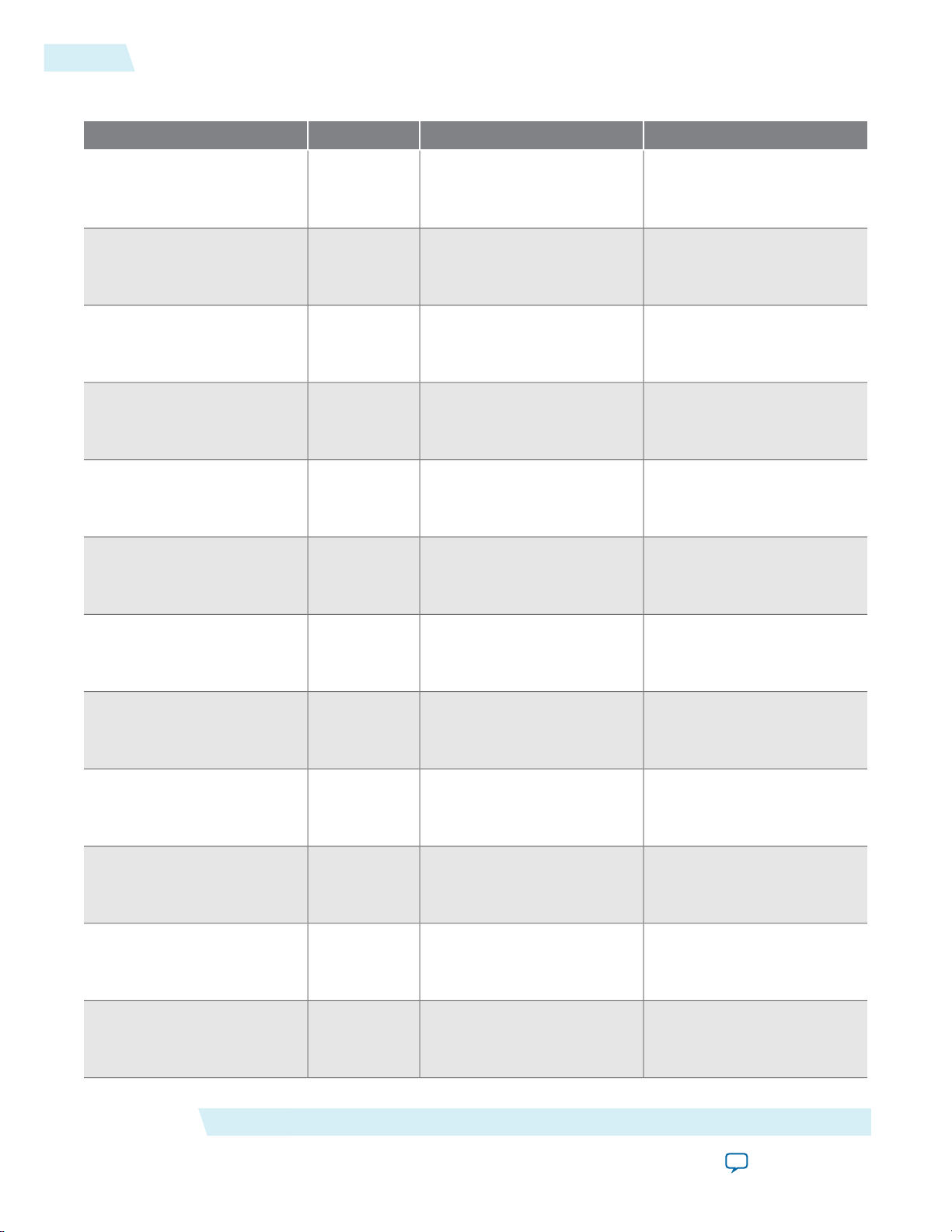
Table 1: On-Chip Debugging Tool Suite
SignalTap II Logic Analyzer
SignalProbe
Logic Analyzer Interface (LAI)
Uses FPGA resources to sample tests
nodes andoutputs the information to
the Quartus II software for display
and analysis.
Incrementally routes internal signals
to I/O pins while preserving the
results from your last place-androute.
Multiplexes a larger set of signals to
a smaller number of spare I/O pins.
LAI allows you to selectwhich signals
are switched onto the I/O pins over a
JTAG connection.
Typical Circumstances for UseDescriptionTool
You have spare on-chip memory
and want functional verification
of your design running in
hardware.
You have spare I/O pins and want
to check the operation of a small
set of control pins using either an
external logic analyzer or an
oscilloscope.
You havelimited on-chip memory
and have a large set of internal
data buses that you want to verify
using an external logic analyzer.
Logic analyzer vendors, such as
Tektronics and Agilent, provide
integration with the tool to
improve usability.
Altera Corporation
Virtual JTAG Megafunction (sld_virtual_jtag)
Send Feedback
Page 3
Logic
Logic
JTAG
sld_virtual_jtag
sld_virtual_jtag
tck
tms
trst
tdi
tdo
UG-SLDVRTL
2014.03.19
Applications of the Virtual JTAG Megafunction
Typical Circumstances for UseDescriptionTool
3
In-System Memory Content
Editor
In-System Sources and Probes
Displays and allows you to edit onchip memory.
Provides a way to drive and sample
logic values to and from internal
nodes using the JTAG interface.
Virtual JTAG Interface
Opens the JTAGinterface so that you
can develop your own custom
applications.
Related Information
System Debugging Tools Overview
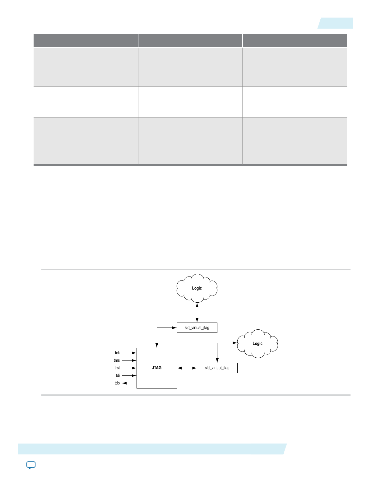
Applications of the Virtual JTAG Megafunction
You caninstantiate single ormultiple instances of theVirtual JTAG megafunctionin your HDL code.During
synthesis, the Quartus II software assigns unique IDs to each instance, so that each instance is accessed
individually. You can instantiate up to 128 instances of the Virtual JTAG megafunction. The figure below
shows a typical application in a design with multiple instances of the megafunction.
You want to view and edit the
contents of either the instruction
cache or data cache of a Nios®II
processor application.
You want to prototype a front
panel withvirtual buttons foryour
FPGA design.
You want to generate a large set
of test vectors and send them to
your deviceover the JTAG port to
functionally verify your design
running in hardware.
Figure 1: Application Example
The SLD hub automatically arbitrates between multiple applications that share a single JTAG resource.
Therefore, you can use the megafunction in tandem with other on-chip debugging applications, such as the
SignalTap II Logic Analyzer, to increase debugging visibility. You can also use the megafunction to provide
Virtual JTAG Megafunction (sld_virtual_jtag)
Send Feedback
Altera Corporation
Page 4
Serial
Data In
JTAG Device 1 JTAG Device 2
Serial
Data Out
Core
Logic
Core
Logic
Boundary-Scan Cell
IC Pin Signal
Interconnection
to be Tested
4
JTAG Protocol
simple stimulus patterns to solicit a response from the design under test during run-time, including the
following applications:
• To diagnose, sample, and update the values of internal parts of your logic. With this megafunction, you
can easily sample and update the values of the internal counters and state machines in your hardware
device.
• To build your own customsoftware debugging IP using the Tcl commands to debug your hardware. This
IP communicates with the instances of the Virtual JTAG megafunction inside your design.
• To construct your design to achieve virtual inputs and outputs.
• If youare building a debuggingsolution for a systemin which a microprocessor controls the JTAG chain,
you cannotuse the SignalTap IILogic Analyzer because theJTAG control must be withthe microprocessor.
You can use low-level controls for the JTAG port from the Tcl commands to direct microprocessors to
communicate with the Virtual JTAG megafunction inside the device core.
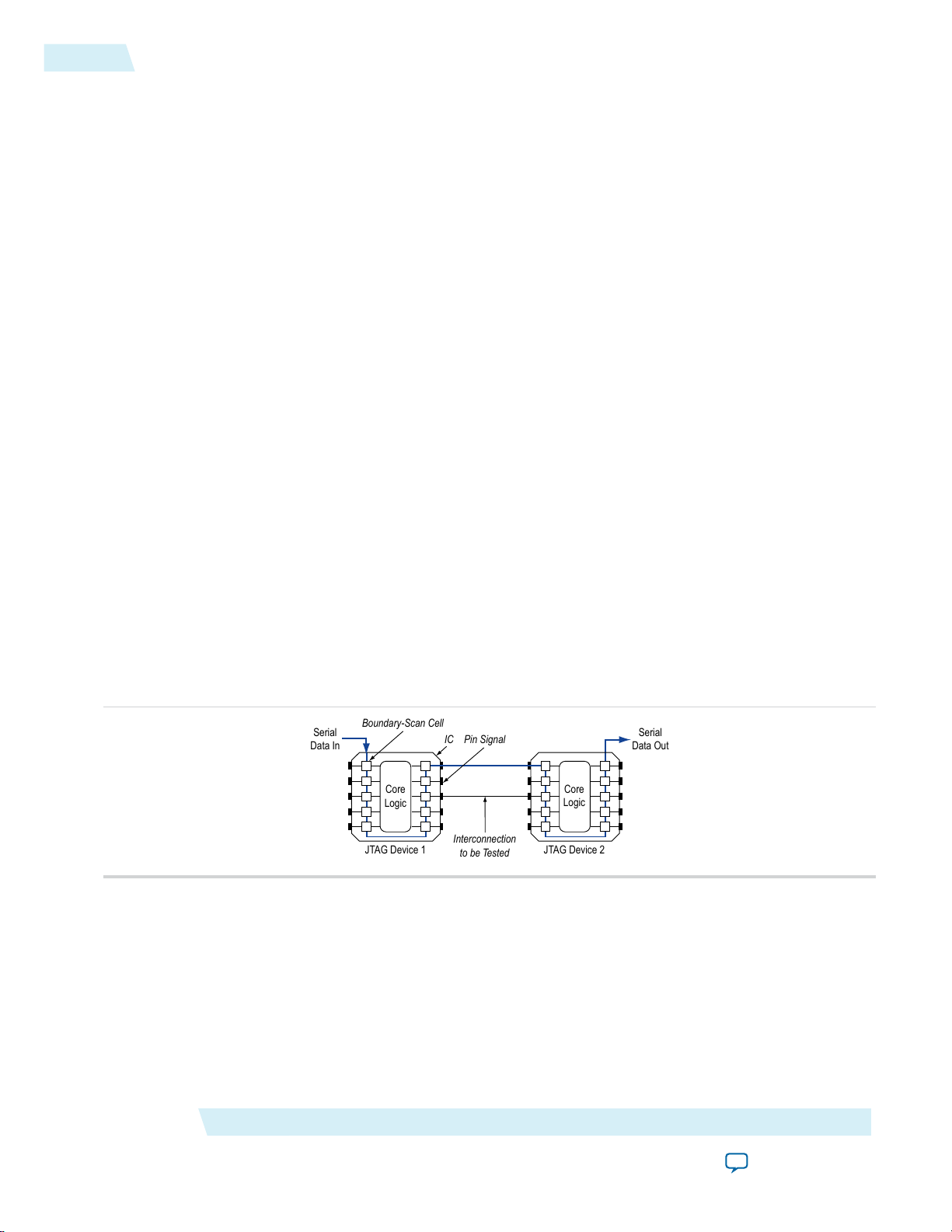
JTAG Protocol
The original intent of theJTAG protocol (standardized as IEEE 1149.1) wasto simplify PCBinterconnectivity
testing during the manufacturing stage. As access to integrated circuit (IC) pins became more limited due
to tighter lead spacing and FPGA packages, testing through traditional probing techniques, such as
“bed-of-nails” test fixtures, became infeasible. The JTAG protocol alleviates the need for physical access to
IC pins via a shift register chain placed near the I/O ring. This set of registers near the I/O ring, also known
as boundary scan cells (BSCs), samples and forces values out onto the I/O pins. The BSCs from
JTAG-compliant ICs are daisy-chained into a serial-shift chain and driven via a serial interface.
UG-SLDVRTL
2014.03.19
During boundary scan testing, software shifts out test data over the serial interface to the BSCs of select ICs.
This test data forces a known pattern to the pins connected to the affected BSCs. If the adjacent IC at the
other end of the PCB trace is JTAG-compliant, the BSC of the adjacent IC samples the test pattern and feeds
the BSCs back to the software for analysis. The figure below illustrates the boundary-scan testing concept.
Figure 2: IEEE Std. 1149.1 Boundary-Scan Testing
Because the JTAG interface shifts in any information to the device, leaves a low footprint, and is available
on all Altera devices, it is considered a general purpose communication interface. In addition to boundary
scan applications, Altera devices use the JTAG port for other applications, such as device configuration and
on-chip debugging features available in the Quartus II software.
Related Information
IEEE 1149.1 JTAG Boundary-Scan Testing
Altera Corporation
Virtual JTAG Megafunction (sld_virtual_jtag)
Send Feedback
Page 5

UG-SLDVRTL
2014.03.19
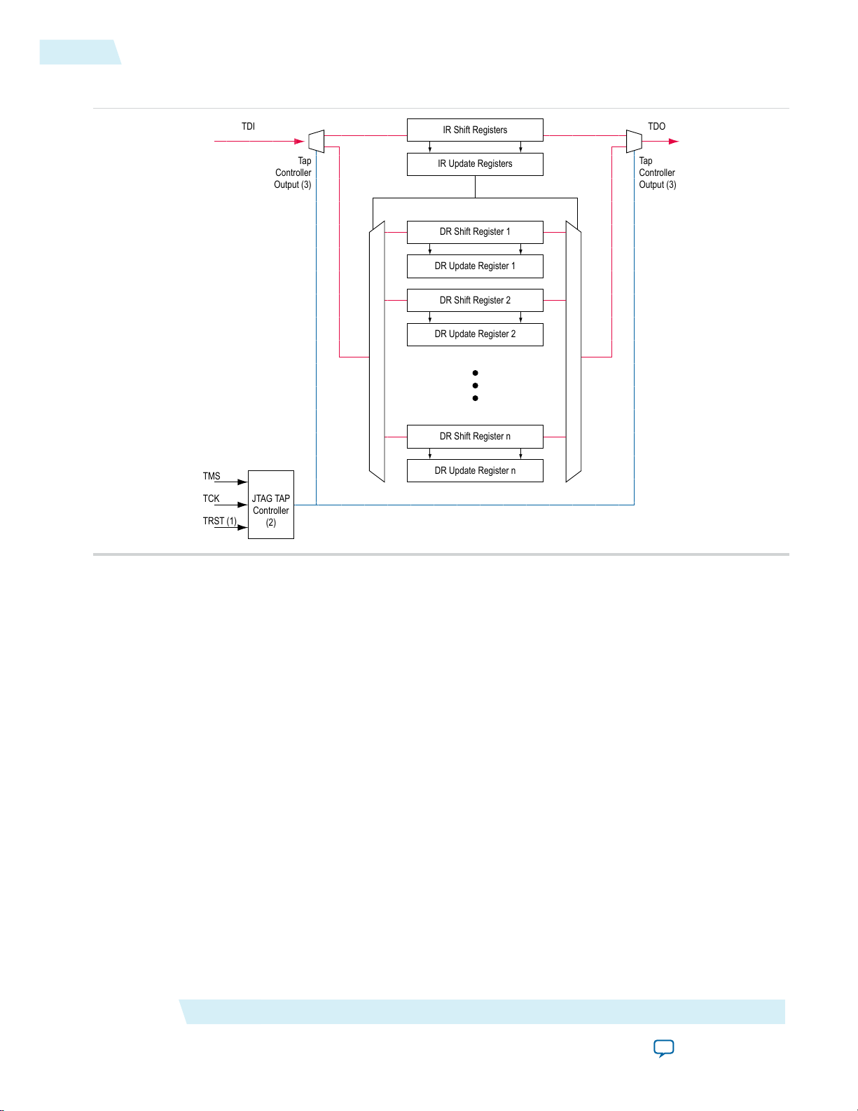
JTAG Circuitry Architecture
The basic architecture of the JTAG circuitry consists of the following components:
• A set of Data Registers (DRs)
• An Instruction Register (IR)
• A state machine to arbitrate data (known as the Test Access Port (TAP) controller)
• A four- or five-pin serial interface, consisting of the following pins:
• Test data in (TDI), used to shift data into the IR and DR shift register chains
• Test data out (TDO), used to shift data out of the IR and DR shift register chains
• Test mode select (TMS), used as an input into the TAP controller
• TCK, used as the clock source for the JTAG circuitry
• TRST resets the TAP controller. This is an optional input pin defined by the 1149.1 standard.
The TRST pin is not present in the Cyclone device family.Note:
The bank of DRs is the primary data path of the JTAG circuitry. It carries the payload data for all JTAG
transactions. Each DRchain is dedicated to serving a specific function. Boundaryscan cells form the primary
DR chain. The other DR chains are used for identification, bypassing the IC during boundary scan tests, or
a custom set of register chains with functions defined by the IC vendor. Altera uses two of the DR chains
with user-defined IP that requires the JTAG chain as a communication resource, such as the on-chip
debugging applications. The Virtual JTAG megafunction, in particular, allows you to extend the two DR
chains to a user-defined custom application.
JTAG Circuitry Architecture
5
You use the instruction register to select the bank of Data Registers to which the TDI and TDO must connect.
It functions as an address register for the bank of Data Registers. Each IR instruction maps to a specific DR
chain.
All shift registers that area part of the JTAG circuitry (IR and DR register chains) are composedof two kinds
of registers: shift registers, which capture new serial shift input from the TDI pin, and parallel hold registers,
which connect to each shift register to hold the current input in place when shifting. The parallel hold
registers ensure stability in the output when new data is shifted.
The figure below shows a functional model of the JTAG circuitry. The TRST pin is an optional pin in the
1149.1 standard and not available in Cyclone devices. The TAP controller is a hard controller; it is not created
using programmable resources. The major function of the TAP controller is to route test data between the
IR and DR register chains.
Virtual JTAG Megafunction (sld_virtual_jtag)
Send Feedback
Altera Corporation
Page 6
IR Shift Registers
IR Update Registers
DR Shift Register 1
DR Update Register 1
DR Shift Register 2
DR Update Register 2
DR Shift Register n
DR Update Register n
JTAG TAP
Controller
(2)
TDI TDO
Tap
Controller
Output (3)
Tap
Controller
Output (3)
TRST (1)
TCK
TMS
6
System-Level Debugging Infrastructure
Figure 3: Functional Model of the JTAG Circuitry
UG-SLDVRTL
2014.03.19
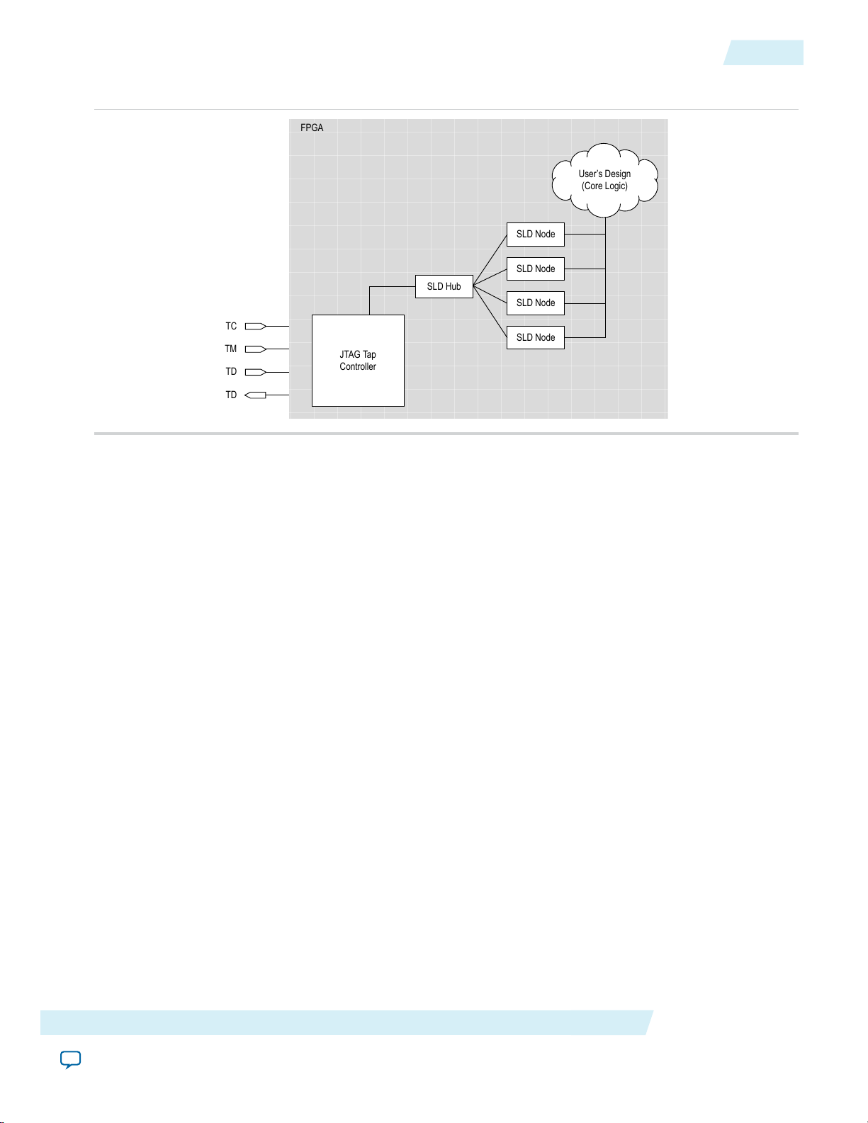
System-Level Debugging Infrastructure
On-chip debugging tools that require the JTAG resources share two Data Register chain paths; USER1 and
USER0 instructions select the Data Register chain paths. The datapaths are anextension of theJTAG circuitry
for use with the programmable logic elements in Altera devices.
Altera Corporation
Because the JTAG resource is shared among multiple on-chip applications, an arbitration scheme must
define how the USER0 and USER1 scan chains are allocated between the different applications. The systemlevel debugging (SLD) infrastructure defines the signaling convention and the arbitration logic for all
programmable logic applications using a JTAG resource. The figure below shows the SLD infrastructure
architecture.
Virtual JTAG Megafunction (sld_virtual_jtag)
Send Feedback
Page 7
JTAG Tap
Controller
TC
TM
TD
TD
FPGA
SLD Node
SLD Node
SLD Node
SLD Node
SLD Hub
User’s Design
(Core Logic)
UG-SLDVRTL
2014.03.19
Transaction Model of the SLD Infrastructure
Figure 4: System Level Debugging Infrastructure Functional Model
7
Transaction Model of the SLD Infrastructure
In the presence of an application that requires the JTAG resource, the Quartus II software automatically
implements the SLD infrastructure to handle the arbitration of the JTAG resource. The communication
interface between JTAG and any IP cores is transparent to the designer. All components of the SLD
infrastructure, except for the JTAG TAP controller, are built using programmable logic resources.
The SLD infrastructure mimics the IR/DR paradigm defined by the JTAG protocol. Each application
implements an Instruction Register, and a set of Data Registers that operate similarly to the Instruction
Register and Data Registers in the JTAG standard. Note that the Instruction Register and the Data Register
banks implemented by each application are a subset of the USER1 and USER0 Data Register chains. The SLD
infrastructure consists of three subsystems: the JTAG TAP controller, the SLD hub, and the SLD nodes.
The SLD hub acts as the arbiter that routes the TDI pin connection between each SLD node, and is a state
machine that mirrors the JTAG TAP controller state machine.
The SLDnodes represent thecommunication channels for theend applications. Each instanceof IP requiring
a JTAGcommunication resource, such as theSignalTap II Logic Analyzer, wouldhave its own communication
channel in the form of a SLD node interface to the SLD hub. Each SLD node instance has its own Instruction
Register and bank of DR chains. Up to 255 SLD nodes can be instantiated, depending on resources available
in your device.
Together, the sld_hub and the SLD nodes form a virtual JTAG scan chain within the JTAG protocol. It is
virtual in the sense that both the Instruction Register and DR transactions for each SLD node instance are
encapsulated within a standard DR scan shift of the JTAG protocol.
The Instruction Register and Data Registers for the SLD nodes are a subset of the USER1 and USER0 Data
Registers. Because the SLD Node IR/DR register set is not directly part of the IR/DR register set of the JTAG
protocol, the SLD node Instruction Register and Data Register chains are known as Virtual IR (VIR) and
Virtual DR (VDR) chains. The figure below shows the transaction model of the SLD infrastructure.
Virtual JTAG Megafunction (sld_virtual_jtag)
Send Feedback
Altera Corporation
Page 8
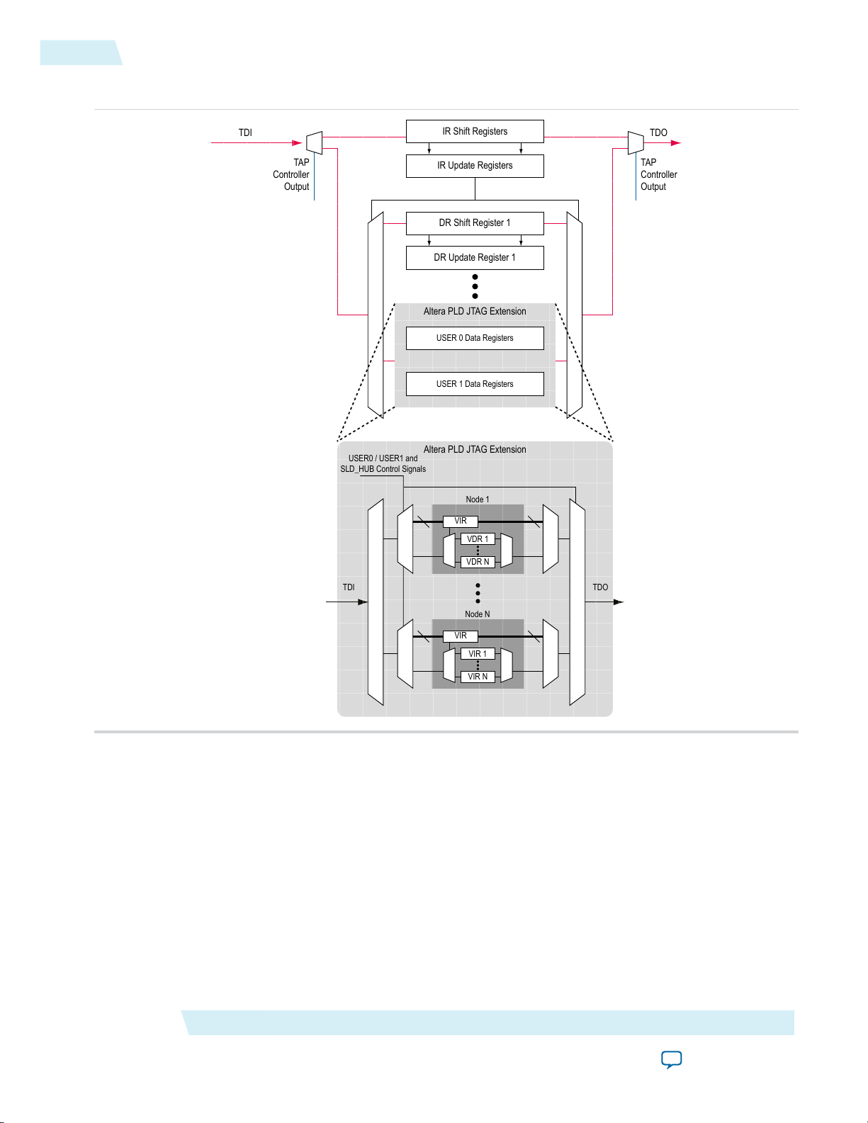
IR Shift Registers
IR Update Registers
DR Shift Register 1
DR Update Register 1
USER 0 Data Registers
USER 1 Data Registers
TDI TDO
TAP
Controller
Output
TAP
Controller
Output
Altera PLD JTAG Extension
Altera PLD JTAG Extension
Node 1
Node N
USER0 / USER1 and
SLD_HUB Control Signals
TDI TDO
VIR
VDR 1
VDR N
VIR
VIR 1
VIR N
8
SLD Hub Finite State Machine
Figure 5: Extension of the JTAG Protocol for PLD Applications
UG-SLDVRTL
2014.03.19
SLD Hub Finite State Machine
The SLDhub decodes TMS independently from the hard JTAGTAP controller state machineand implements
an equivalent state machine (calledthe “SLD hubfinite state machine”) for the internal JTAG path. The SLD
hub performs a similar function for the VIR and VDR chains that the TAP controller performs for the JTAG
IR and DR chains. It enables an SLD node as the active path for the TDI pin, selects the TDI data between
the VIR and VDR registers, controls the start and stop of any shift transactions, and controls the data flow
between the parallel hold registers and the parallel shift registers of the VIR and VDR.
Because all shifts to VIR and VDR are encapsulated within a DR shift transaction, an additional control
signal is necessary to select between the VIR and VDR data paths. The SLD hub uses the USER1 command
to select the VIR data path and the USER0 command to select the VDR data path.
Altera Corporation
Virtual JTAG Megafunction (sld_virtual_jtag)
Send Feedback
Page 9
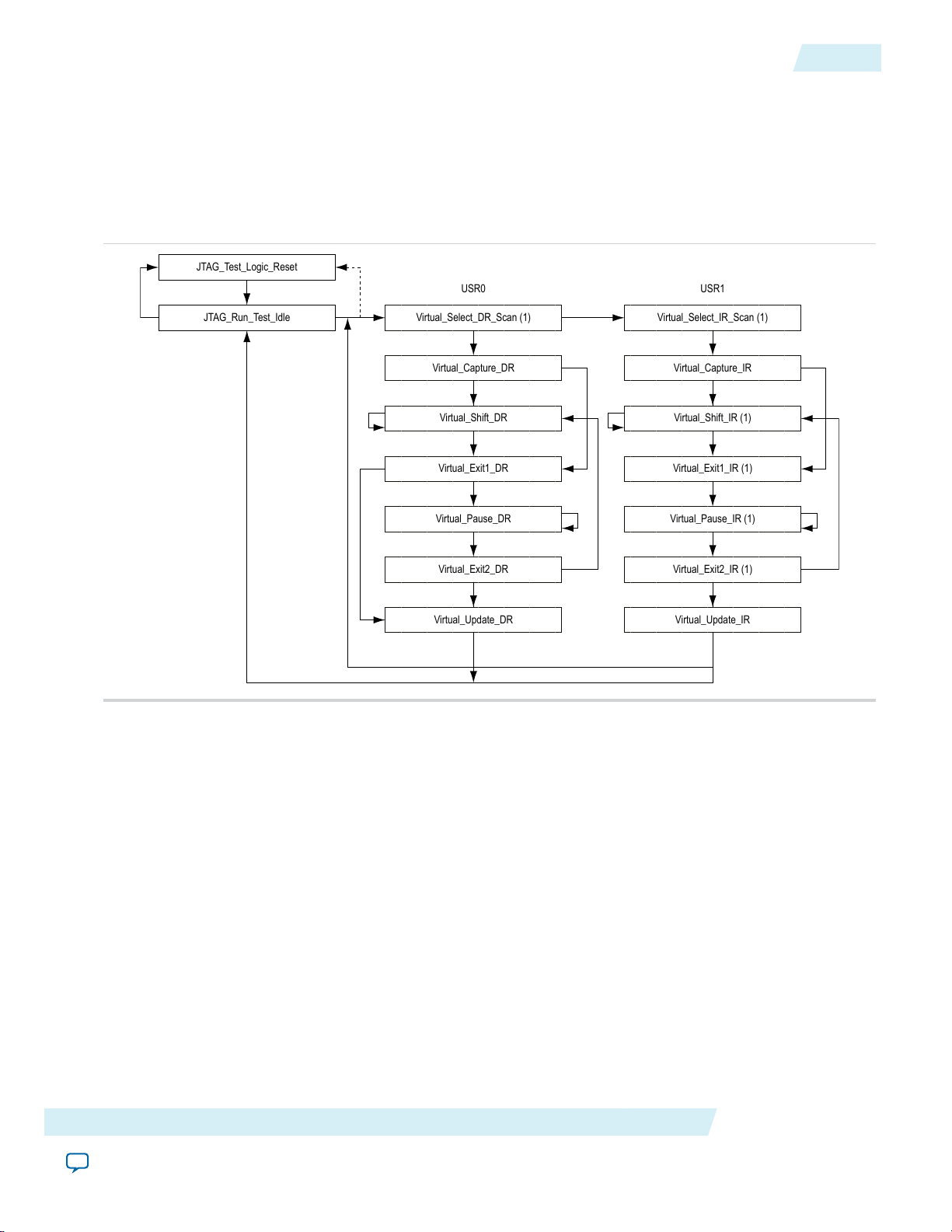
USR0 USR1
JTAG_Test_Logic_Reset
JTAG_Run_Test_Idle Virtual_Select_DR_Scan (1) Virtual_Select_IR_Scan (1)
Virtual_Capture_DR
Virtual_Shift_DR
Virtual_Exit1_DR
Virtual_Pause_DR
Virtual_Exit2_DR
Virtual_Update_DR
Virtual_Capture_IR
Virtual_Shift_IR (1)
Virtual_Exit1_IR (1)
Virtual_Pause_IR (1)
Virtual_Exit2_IR (1)
Virtual_Update_IR
UG-SLDVRTL
2014.03.19
Description of the Virtual JTAG Interface
This state information, including a bank of enable signals, is forwarded to each of the SLD nodes. The SLD
nodes perform the updates to the VIR and VDR according to the control states provided by the sld_hub.
The SLD nodes are responsible for maintaining continuity between the TDI and TDO pins.
The figure below shows the SLD hub finite state machine. There is no direct state signal available to use for
application design.
Figure 6: sld_hub Finite State Machine
9
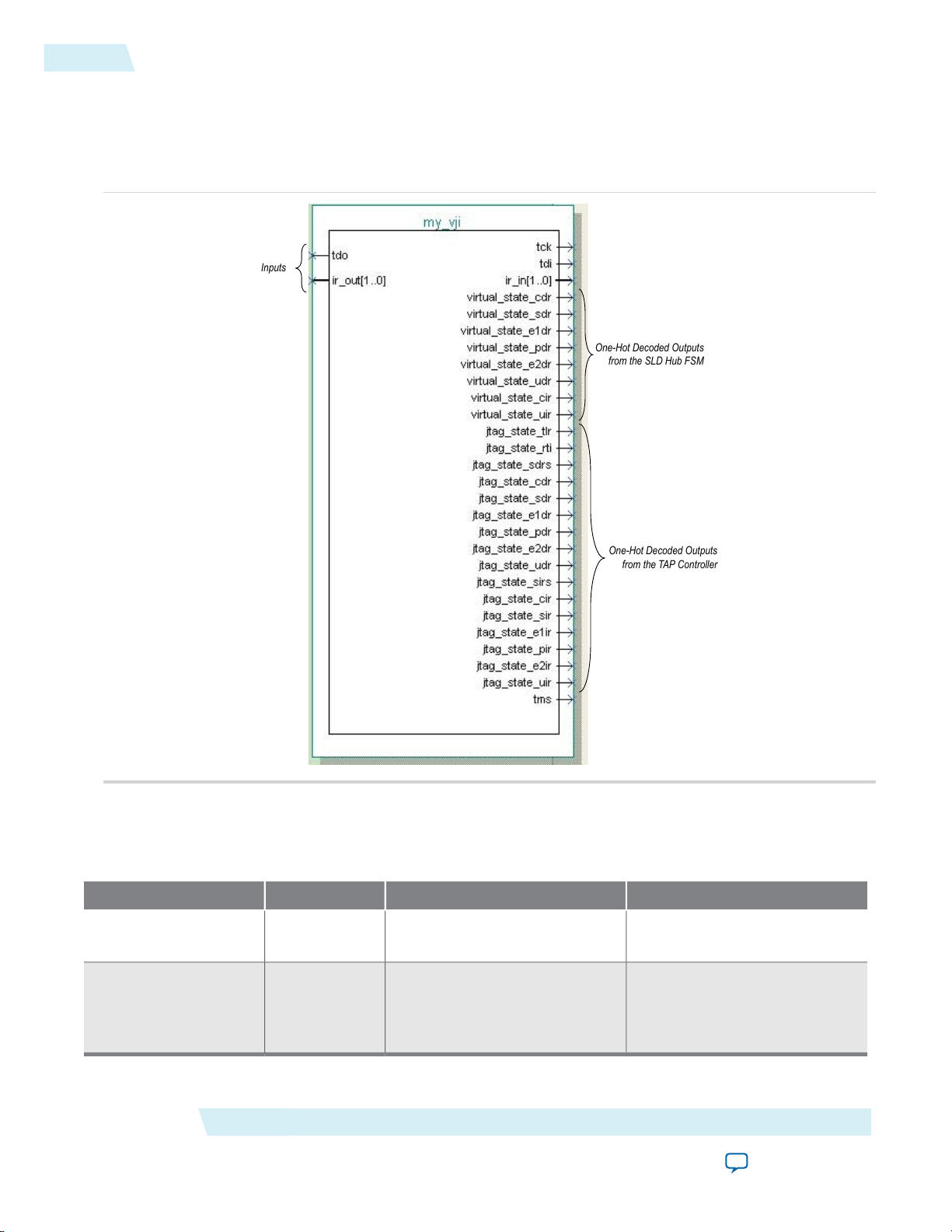
Description of the Virtual JTAG Interface
The Virtual JTAG Interface implements an SLD node interface, which provides a communication interface
Virtual JTAG Megafunction (sld_virtual_jtag)
to the JTAG port. The megafunction exposes control signals that are part of the SLD hub; namely, JTAG
port signals, all finite state machine controller states of the TAP controller, and the SLD hub finite state
machine. Additionally, each instance of the Virtual JTAG megafunctions contain the virtual Instruction
Register for the SLD node. Instantiation of this megafunction automatically infers the SLD infrastructure,
and one SLD node is added for each instantiation.
The Virtual JTAG megafunction provides a port interface that mirrors the actual JTAG ports. The interface
contains the JTAG port pins, a one-hot decoded output of all JTAG states, and a one-hot decoded output
of all the virtual JTAG states. Virtual JTAG states are the states decoded from the SLD hub finite state
machine. The ir_in and ir_out ports are the parallel input and output to and from the VIR. The VIR ports
are used toselect theactive VDR datapath. The JTAG states and TMSoutput ports are provided for debugging
purposes only. Only the virtual JTAG, TDI, TDO, and the IR signals are functional elements of the
megafunction. When configuring this megafunction using the MegaWizard™Plug-In Manager, you can
hide TMS and the decoded JTAG states.
Send Feedback
Altera Corporation
Page 10
Inputs
One-Hot Decoded Outputs
from the SLD Hub FSM
One-Hot Decoded Outputs
from the TAP Controller
10
Input Ports
The figure below shows the input and output ports of the virtual JTAG megafunction. The JTAG TAP
controller outputs and TMS signals are used for informational purposes only. These signals can be exposed
using the Create primitive JTAG state signal ports option on page 3 of the MegaWizard Plug-In Manager.
Figure 7: Input and Output Ports of the Virtual JTAG Megafunction
UG-SLDVRTL
2014.03.19
Input Ports
Table 2: Input Ports for the Virtual JTAG Megafunction
Yestdo
Writes to the TDO pin on the
device.
Noir_out[]
Virtual JTAG instruction register
output. The value is captured
whenever virtual_state_cir is
high.
Altera Corporation
CommentsDescriptionRequiredPort name
Input port [SLD_IR_WIDTH-
1..0] wide. Specify the width
of this bus with the SLD_IR_
WIDTH parameter.
Virtual JTAG Megafunction (sld_virtual_jtag)
Send Feedback
Page 11
UG-SLDVRTL
2014.03.19
Output Ports
Table 3: Output Ports for the Virtual JTAG Megafunction
Output Ports
CommentsDescriptionRequiredPort Name
11
JTAG test clock.Yestck
Yestdi
TDI inputdata on the device.Used
when virtual_state_sdr is high.
Noir_in[]
Virtual JTAG instruction register
data. The value is available and
latched when virtual_state_uir
is high.
Table 4: High-Level Virtual JTAG State Signals
Novirtual_state_cdr
Yesvirtual_state_sdr
Novirtual_state_e1dr
Indicates thatvirtual JTAG is in
Capture_DR state.
Indicates thatvirtual JTAG is in
Shift_DR state.
Indicates thatvirtual JTAG is in
Exit1_DR state.
Connected directly to the TCK
device pin. Shared among all
virtual JTAG instances.
Shared amongall virtual JTAG
instances.
Output port [SLD_IR_WIDTH-
1..0] wide. Specify the width
of this bus with the SLD_IR_
WIDTH parameter.
CommentsDescriptionRequiredPort Name
In this state, this instance is
required to establish the
JTAG chain for this device.
Virtual JTAG Megafunction (sld_virtual_jtag)
Novirtual_state pdr
Indicates thatvirtual JTAG is in
Pause_DR state.
The QuartusII software does
not cycle through this state
using the Tcl command.
Novirtual_state_e2dr
Indicates thatvirtual JTAG is in
Exit2_DR state.
The QuartusII software does
not cycle through this state
using the Tcl command.
Novirtual_state_udr
Indicates thatvirtual JTAG is in
Update_DR state.
Novirtual_state_cir
Indicates thatvirtual JTAG is in
Capture_IR state.
Novirtual_state_uir
Indicates thatvirtual JTAG is in
Update_IR state.
Altera Corporation
Send Feedback
Page 12
12
Output Ports
Table 5: Low-Level Virtual JTAG State Signals
UG-SLDVRTL
2014.03.19
CommentsDescriptionRequiredPort Name
Nojtag_state_tlr
Indicates that the device JTAG
controller is in the Test_Logic_
Shared among all virtual
JTAG instances.
Reset state.
Nojtag_state_rti
Indicates that the device JTAG
controller is in the Run_Test/
Shared among all virtual
JTAG instances.
Idle state.
Nojtag_state_sdrs
Indicates that the device JTAG
controller is in the Select_DR_
Shared among all virtual
JTAG instances.
Scan state.
Nojtag_state_cdr
Indicates that the device JTAG
controller is in the Capture_DR
Shared among all virtual
JTAG instances.
state.
Nojtag_state_sdr
Indicates that the device JTAG
controller is in the Shift_DR
Shared among all virtual
JTAG instances.
state.
Nojtag_state_e1dr
Indicates that the device JTAG
controller is in the Exit1_DR
Shared among all virtual
JTAG instances.
state.
Nojtag_state_pdr
Indicates that the device JTAG
controller is in the Pause_DR
Shared among all virtual
JTAG instances.
state.
Nojtag_state_e2dr
Indicates that the device JTAG
controller is in the Exit2_DR
Shared among all virtual
JTAG instances.
state.
Nojtag_state_udr
Indicates that the device JTAG
controller is in the Update_DR
Shared among all virtual
JTAG instances.
state.
Nojtag_state_sirs
Indicates that the device JTAG
controller is in the Select_IR_
Shared among all virtual
JTAG instances.
Scan state.
Nojtag_state_cir
Indicates that the device JTAG
controller is in the Capture_IR
Shared among all virtual
JTAG instances.
state.
Nojtag_state_sir
Indicates that the device JTAG
controller is in the Shift_IR
Shared among all virtual
JTAG instances.
state.
Altera Corporation
Virtual JTAG Megafunction (sld_virtual_jtag)
Send Feedback
Page 13
UG-SLDVRTL
2014.03.19
Parameters
CommentsDescriptionRequiredPort Name
13
Nojtag_state_e1ir
Indicates that the device JTAG
controller is in the Exit1_IR
state.
Nojtag_state_pir
Indicates that the device JTAG
controller is in the Pause_IR
state.
Nojtag_state_e2ir
Indicates that the device JTAG
controller is in the Exit2_IR
state.
jtag_state_uir
Indicates that the device JTAG
controller is in the Update_IR
state.
TMS input pin on the device.tms
Parameters
Table 6: Parameters for the Virtual JTAG Megafunction
Shared among all virtual
JTAG instances.
Shared among all virtual
JTAG instances.
Shared among all virtual
JTAG instances.
Shared among all virtual
JTAG instances.
Shared among all virtual
JTAG instances.
DescriptionRequiredTypeParameter
YesStringSLD_AUTO_INSTANCE_INDEX
Specifies whether the Compiler automatically
assigns an index to the Virtual JTAG instance.
Values are YES or NO. When you specify NO,
you can find the auto assigned value of
INSTANCE_ID in the quartus_map file. When
you specify NO, you must define INSTANCE_
INDEX. If the index specified is not unique in a
design, the Compiler automatically reassigns
an index to the instance. The default value is
YES.
NoIntegerSLD_INSTANCE_INDEX
Specifies a unique identifier for every instance
of alt_virtual_jtag when AUTO_INSTANCE_
ID is specified to YES. Otherwise, this value is
ignored.
YesIntegerSLD_IR_WIDTH
Specifies the width of the instruction register
ir_in[] of this virtual JTAG between 1 and 24.
If omitted, the default is 1.
Virtual JTAG Megafunction (sld_virtual_jtag)
Send Feedback
Altera Corporation
Page 14

14
Design Flow of the Virtual JTAG Megafunction
Design Flow of the Virtual JTAG Megafunction
Designing with the Virtual JTAG megafunction includes the following processes:
• Configuring theVirtual JTAG megafunctionwith the desired InstructionRegister length and instantiating
the megafunction.
• Building the glue logic for interfacing with your application.
• Communicating with the Virtual JTAG instance during runtime.
In additionto the JTAG datapath andcontrol signals, the Virtual JTAGmegafunction encompasses the VIR.
The Instruction Register size is configured in the MegaWizard Plug-In Manager. The Instruction Register
port on the Virtual JTAG megafunction is the parallel output of the VIR. Any updated VIR information can
be read from this port after the virtual_state_uir signal is asserted.
After instantiating the megafunction, you must create the VDR chains that interface with your application.
To do this, you use the virtual instruction output to determine which VDR chain is the active datapath, and
then create the following:
• Decode logic for the VIR
• VDR chains to which each VIR maps
• Interface logic between your VDR chains and your application logic
Your glue logic uses the decoded one-hot outputs from the megafunction to determine when to shift and
when to update the VDR. Your application logic interfaces with the VDR chains during any one of the nonshift virtual JTAG states.
UG-SLDVRTL
2014.03.19
For example, your application logic can parallel read an updated value that was shifted in from the JTAG
port after the virtual_state_uir signal is asserted. If you load a value to be shifted out of the JTAG port,
you would do so when the virtual_state_cdr signal is asserted. Finally, if you enable the shift register to
clock out information to TDO, you would do so during the assertion of virtual_state_sdr.
Maintaining TDI-to-TDOconnectivity is important.Ensure that allpossible instruction codesmap to an active
register chain to maintain connectivity in the TDI-to-TDO datapath. Altera recommends including a bypass
register as the active register for all unmapped IR values.
Note that TCK(a maximum 10-MHz clock, if using an Altera programming cable) provides the clock for the
entire SLD infrastructure. Be sure to follow best practices for proper clock domain crossing between the
JTAG clock domain and the rest of your application logic to avoid metastability issues. The decoded virtual
JTAG state signals can help determine a stable output in the VIR and VDR chains.
After compiling and downloading your design into the device, you can perform shift operations directly to
the VIR and VDR chains using the Tcl commands from the quartus_stp executable and an Altera
programming cable (for example, a USB-Blaster™, a MasterBlaster™, or a ByteBlaster™II cable). The
quartus_stp executable is a command-line executable that contains Tcl commands for all on-chip debug
features available in the Quartus II software.
The figure below shows the components of a design containing one instance of the Virtual JTAG
megafunction. The TDI-to-TDO datapath for the virtual JTAG chain, shown in red, consists of a bank of DR
registers. Input to the application logic is the parallel output of the VDR chains. Decoded state signals are
used to signal start and stop of shift transactions and signals when the VDR output is ready.
The IR_out port, not shown, is an optional input port you can use to parallel load the VIR from the FPGA
core logic.
Altera Corporation
Virtual JTAG Megafunction (sld_virtual_jtag)
Send Feedback
Page 15

Inferred by Instantiation
of Megafunction
Glue Logic between VJI and User Design
(Created by Designer)
Original Design
Application
Logic
SLD
Hub
VJI Megafunction
Instance
IR
JTAG TAP
Controller
TDI
TDO
TMS
TCK
TRST
TMS & Decoded
State Signals
IR_in
TDI
TDO
Input Vector 1
Input Vector 2
Input Vector n
VDR Chain 1
VDR Chain 2
VDR Chain n
UG-SLDVRTL
2014.03.19
Figure 8: Block Diagram of a Design with a Single Virtual JTAG Instantiation
Simulation Model
15
Virtual JTAG Megafunction (sld_virtual_jtag)
Simulation Model
The virtual JTAG megafunction contains a functional simulation model that provides stimuli that mimic
VIR and VDR shifts. You can configure the stimuli using the MegaWizard Plug-In Manager. You can use
this simulation model for functional verification only, and the operation of the SLD hub and the SLD
node-to-hub interface is not provided in this simulation model.
Run-Time Communication with the Virtual JTAG Megafunction
The Tcl API for the Virtual JTAG megafunction consists of a set of commands for accessing the VIR and
VDR of each virtual JTAG instance.
These commands contain the underlying drivers for accessing an Altera programming cable and for issuing
shift transactions to each VIR and VDR. The table below provides the Tcl commands in the quartus_stp
executable that you can use with the Virtual JTAG megafunction, and are intended for designs that use a
custom controller to drive the JTAG chain.
Each instantiationof the VirtualJTAG megafunction includes aninstance index. Allinstances are sequentially
numbered and are automatically provided by the Quartus II software. The instance index starts at instance
index 0. The VIR and VDR shift commands described in the table decode the instance index and provide
an address to the SLD hub for each megafunction instance. You can override the default index provided by
the Quartus II software during configuration of the megafunction.
Send Feedback
The table below provides the Tcl commands in the quartus_stp executable that you can use with the Virtual
JTAG megafunction, and are intended for designs that use a custom controller to drive the JTAG chain.
Altera Corporation
Page 16

16
Run-Time Communication with the Virtual JTAG Megafunction
Table 7: Tcl Commands Used with the Virtual JTAG Megafunction
UG-SLDVRTL
2014.03.19
DescriptionArgumentsCommand
Device virtual ir shift
Device virtual dr shift
Open device
-instance_index <instance_index>
-ir_value <numeric_ir_value>
-no_captured_ir_value
-show_equivalent_device_ir_dr_shift
-instance_index <instance_index>
-dr_value <dr_value>
-length <data_register_length>
-no_captured_dr_value
-show_equivalent_device_ir_dr_shift
-value_in_hex
(1)
(1)
(1)
NONEGet hardware names
-device_name <device_name>
-hardware_name <hardware_name>
NONEClose device
Perform an IR shift operationto the
virtual JTAG instance specified by
the instance_index. Note that ir_
value takes a numerical argument.
(1)
Perform a DR shift operation to the
virtual JTAG instance.
Queries for all available programming cables.
Selects the active device on the
JTAG chain.
Ends communicationwith the active
JTAG device.
-timeout <timeout>Device lock
Obtains exclusive communication
to the JTAG chain.
Releases device_lock.NONEDevice unlock
Device ir shift
-no_captured_ir_value
Device dr shift
-length <data register length>
-no_captured_dr_value
-value_in_hex
Performs a IR shift operation.-ir_value <ir_value>
Performs a DR shift operation.-dr_value <dr_value>
Central to virtual JTAG megafunctionare the device_virtual_ir_shift and device_virtual_dr_shift
commands. These commands perform the shift operation to each VIR/VDR and provide the address to the
SLD hub for the active JTAG datapath.
(1)
This argument is optional.
Altera Corporation
Virtual JTAG Megafunction (sld_virtual_jtag)
Send Feedback
Page 17

UG-SLDVRTL
2014.03.19
Running a DR Shift Operation Through a Virtual JTAG Chain
17
Each device_virtual_ir_shift command issues a USER1 instruction to the JTAG Instruction Register
followed by a DR shift containing the VIR value provided by the ir_value argument prepended by address
bits to target the correct SLD node instance.
Note:
Use the -no_captured_ir_valueargument if you do not care about shifting out the contents of the
current VIR value. Enabling this argument increases the speed of the VIR shift transaction by
eliminating a command cycle within the underlying transaction.
Similarly, each device_virtual_dr_shift command issues a USER0 instruction to the JTAG Instruction
Register followed by a DR shift containing the VDR value provided by the dr_value argument. These
commands return the underlying JTAG transactions with the show_equivalent_device_ir_dr_shift
option set.
Note:
The device_virtual_ir_shift takes the ir_value argument as a numeric value. The
device_virtual_dr_shift takes the dr_value argument by either a binary string or a hexadecimal
string. Do not use numeric values for the device_virtual_dr_shift.
Running a DR Shift Operation Through a Virtual JTAG Chain
A simple DR shift operation through a virtual JTAG chain using an Altera download cable consists of the
following steps:
1. Query for the Altera programming cable and select the active cable.
2. Target the desired device in the JTAG chain.
3. Obtain a device lock for exclusive communication to the device.
4. Perform a VIR shift.
5. Perform a VDR shift.
6. Release exclusive link with the device with the device_unlock command.
7. Close communication with the device with the close_device command.
Run-Time Communication without Using an Altera Programming Cable
The Virtual JTAG megafunction Tcl API requires an Altera programming cable. Designs that use a custom
controller to drive the JTAG chain directly must issue the correct JTAG IR/DR transactions to target the
Virtual JTAG megafunction instances. The address values and register length information for each Virtual
JTAG megafunction instance are provided in the compilation reports.
The following figureshows the compilation report for aVirtual JTAG megafunction Instance. The following
table describes each column in the Virtual JTAG Settings compilation report.
Virtual JTAG Megafunction (sld_virtual_jtag)
Send Feedback
Altera Corporation
Page 18

18
Run-Time Communication without Using an Altera Programming Cable
Figure 9: Compilation Report
UG-SLDVRTL
2014.03.19
Table 8: Virtual JTAG Settings Description
Instance Index
IR Width
Address
USER1 DR Length
VIR Capture Instruction
The Tcl API provides a way to return the JTAG IR/DR transactions by using the
show_equivalent_device_ir_dr_shift argument with the device_virtual_ir_shift and
device_virtual_dr_shift commands. The following examples use returned values of a virtual IR/DR shift
to illustrate the format of the underlying transactions.
DescriptionSetting
Instance index of the virtual JTAG megafunction. Assigned
at compile time.
Details whether the index was auto-assigned.Auto Index
Details whether the index was user-assigned.Index Re-Assigned
Length of the Virtual IR register for this megafunction
instance; defined in the MegaWizard Plug-In Manager.
The address value assigned to the megafunction by the
compiler.
The length of the USER1 DR register. The USER1 DR register
encapsulates the VIR for all SLD nodes.
Instruction value to capture the VIR of this megafunction
instance.
Altera Corporation
Virtual JTAG Megafunction (sld_virtual_jtag)
Send Feedback
Page 19

UG-SLDVRTL
2014.03.19
Virtual IR/DR Shift Transaction without Returning Captured IR/DR Values
To use the Tcl API to query for the bit pattern in your design, use the
show_equivalent_device_ir_dr_shift argument with the device_virtual_ir_shift and
device_virtual_dr_shift commands.
Both examplesare from thesame design, with asingle Virtual JTAG instance.The VIR lengthfor the reference
Virtual JTAG instance is configured to 3 bits in length.
Virtual IR/DR Shift Transaction without Returning Captured IR/DR Values
VIR shifts consist of a USER1 (0x0E) IR shift followed by a DR shift to the virtual Instruction Register. The
DR Scan shift consists of the value passed by the - dr_value argument. The length and value of the DR shift
is dependent on the number of SLD nodes in your design. This value consists of address bits to the SLD
node instance concatenated with thedesired value ofthe virtual Instruction Register. The addressing scheme
is determined by the Quartus II software during design compilation.
The Tcl command examples below show a VIR/VDR transaction with the no_captured_value option set.
The commands return the underlying JTAG shift transactions that occur.
Virtual IR Shift with the no_captured_value Option
device_virtual_ir_shift -instance_index 0 -ir_value 1 \
-no_captured_ir_value -show_equivalent_device_ir_dr_shift
19
Returns:
Info: Equivalent device ir and dr shift commands
Info: device_ir_shift -ir_value 14
Info: device_dr_shift -length 5 -dr_value 11 -value_in_hex
Virtual DR Shift with the no_captured_value Option
device_virtual_dr_shift -instance_index 0 -length 8 -dr_value \
04 -value_in_hex -no_captured_dr_value \
-show_equivalent_device_ir_dr_shift
Returns:
Info: Equivalent device ir and dr shift commands
Info: device_ir_shift -ir_value 12
Info: device_dr_shift -length 8 -dr_value 04 -value_in_hex
The VIR value field in the figure below is four bits long, even though the VIR length is configured to be three
bits long, and shows the bit values and fields associated with the VIR/VDR scans. The Instruction Register
length for all Altera FPGAs and CPLDs is 10-bits long. The USER1 value is 0x0E and USER0 value is 0x0C for
all Altera FPGAs and CPLDs. The Address bits contained in the DR scan shift of a VIR scan are determined
by the Quartus II software.
All USER1 DR chains must be of uniform length. The length of the VIR value field length is determined by
length of the longest VIR register for all SLD nodes instantiated in the design. Because the SLD hub VIR is
Virtual JTAG Megafunction (sld_virtual_jtag)
Send Feedback
Altera Corporation
Page 20

Virtual IR Scan
Virtual DR Scan
IR Scan Shift
IR Scan Shift
DR Scan Shift
DR Scan Shift
USER1
USER0
VIR Value
VDR Value
Addr
0 0 0 0 0 0 0 0 0
0 0 0 0 0 0 0 0 0 00 0 0
1 1
1 1
0 0
1
1 1 1
0
20
Virtual IR/DR Shift Transaction that Captures Current VIR/VDR Values
four bits long, the minimum length for the VIR value field for all SLD nodes in the design is at least four bits
in length. The Quartus II Tcl API automatically sizes the shift transaction to the correct length. The length
of the VIR register is provided in the Virtual JTAG settings compilation report. If you are driving the JTAG
interface with a custom controller, you must pay attention to size of the USER1 DR chain.
Figure 10: Equivalent Bit Pattern Shifted into Device by VIR/VDR Shift Commands
Virtual IR/DR Shift Transaction that Captures Current VIR/VDR Values
The Tcl command examples below show that the no_captured_value option is not set in the Virtual IR/DR
shift commands and the underlying JTAG shift commands associated with each. In the VIR shift command,
the command returns two device_dr_shift commands.
Virtual IR Shift
UG-SLDVRTL
2014.03.19
device_virtual_ir_shift -instance_index 0 -ir_value 1 \
-no_captured_ir_value -show_equivalent_device_ir_dr_shift
Returns:
Info: Equivalent device ir and dr shift commands
Info: device_ir_shift -ir_value 14
Info: device_dr_shift –length 5 –dr_value 0B –value_in_hex
Info: device_dr_shift -length 5 -dr_value 11 -value_in_hex
Virtual DR Shift
device_virtual_dr_shift -instance_index 0 -length 8 -dr_value \
04 -value_in_hex -show_equivalent_device_ir_dr_shift
Returns:
Info: Equivalent device ir and dr shift commands
Info: device_ir_shift -ir_value 12
Info: device_dr_shift -length 8 -dr_value 04 -value_in_hex
The figure below shows an example of VIR/VDR Shift Commands with captured IR values. DR Scan Shift
1 is the VIR_CAPTURE command, as shown in the figure below. It targets the VIR of the sld_hub. This
Altera Corporation
command is an address cycle to select the active VIR chain to shift after jtag_state_cir is asserted. The
Virtual JTAG Megafunction (sld_virtual_jtag)
Send Feedback
Page 21

Virtual IR Scan
Virtual DR Scan
IR Scan Shift
IR Scan Shift
DR Scan Shift 1
DR Scan Shift
USER1
USER0
VIR Value
VDR Value
Addr
0 0 0 0 0 0 1 0 1
0 0 0 0 0 0 0 0 0 00 0 0
1 1
1 1
0 0
1
1 0 1
0
DR Scan Shift 2
VIR ValueAddr
0 0 0
1 1
UG-SLDVRTL
2014.03.19
Reset Considerations when Using a Custom JTAG Controller
HUB_FORCE_IR capture must be issued whenever you capture theVIR from a target SLD node thatis different
21
than the current active node. DR Scan Shift 1 targets the SLD hub VIR to force a captured value from Virtual
JTAG instance 1 and is shown as the VIR_CAPTURE command. DR Scan Shift 2 targets the VIR of Virtual
JTAG instance.
Figure 11: Equivalent Bit Pattern Shifted into Device by VIR/VDR Shift Commands with Captured IR Values
Note:
If you use an embedded processor as a controller for the JTAG chain and your Virtual JTAG
megafunction instances,consider using the JAM StandardTest and Programming Language (STAPL).
JAM STAPLis an industry-standard flow-control-based language thatsupports JTAG communication
transactions. JAM STAPL is open source, with software downloads and source code available from
the Altera website.
Related Information
• ISP & the Jam STAPL
• Embedded Programming With Jam STAPL
Reset Considerations when Using a Custom JTAG Controller
The SLD hub decodes TMS independently to determine the JTAG controller state. Under normal operation,
the SLD hub mirrors all of the JTAG TAP controller states accurately. The JTAG pins (TCK, TMS, TDI, and
TDO) are accessible to thecore programmable logic; however, the JTAG TAP controller outputs arenot visible
to the core programmable logic. In addition, the hard JTAG TAP controller does not use any reset signals
as inputs from the core programmable logic.
This can cause the following two situations in which control states of the SLD hub and the JTAG TAP
controller are not in lock-step:
• An assertion of the device wide global reset signal (DEV_CLRn)
• An assertion of the TRST signal, if available on the device
DEV_CLRn resets the SLD hub but does not reset the hard TAP controller block. The TAP controller is meant
to be decoupled from USER mode device operation to run boundary scan operations. Asserting the global
reset signal does not disrupt boundary-scan test (BST) operation.
Conversely, the TRST signal, if available, resets the JTAG TAP controller but does not reset the SLD hub.
The TRST signal does not route into the core programmable logic of the PLD.
To guarantee that the states of the JTAG TAP controller and the SLD hub state machine are properly
Virtual JTAG Megafunction (sld_virtual_jtag)
synchronized, TMS should be held high for at least five clock cycles after any intentional reset of either the
Send Feedback
Altera Corporation
Page 22

22
Creating the SLD Virtual JTAG Megafunction
TAP controller orthe systemlogic. Both the JTAG TAP controller and thesld_hub controller are guaranteed
to be in the Test Logic Reset state after five clock cycles of TMS held high.
Creating the SLD Virtual JTAG Megafunction
To create the Virtual JTAG megafunction in a Quartus II design requires the following system and software
requirements:
• The Quartus II software beginning with version 6.0
• MegaWizard Plug-In Manager within the Quartus II software
• An Altera download cable, such as a USB-Blaster cable
The download cable is required to communicate with the Virtual JTAG megafunction from a host running
the quartus_stp executable.
Using the MegaWizard Plug-In Manager
The stimuli specified on Page 4 of the MegaWizard Plug-In Manager are written to the variation file. If you
want to change a stimulus after creating the megafunction, you can either edit the variation file or create the
megafunction again with a new stimulus. The wizard provides an easy way to generate your stimuli. If you
do not want to generate the stimuli, you can skip this step. However, the stimuli are necessary if you are
performing simulation of your design.
UG-SLDVRTL
2014.03.19
Perform the following steps to generate the megafunction:
1. On the Tools menu, click MegaWizard Plug-In Manager. The MegaWizard Plug-In Manager dialog
box appears.
2. Select Create a new custom megafunction variation.
3. Click Next. Page 2a of the MegaWizard Plug-In Manager appears.
4. In the list of megafunctions, click the “+” icon to expand the JTAG-accessible Extensions folder, and
then click Virtual JTAG.
5. Select the device family.
6. Select the type of output file you want to create, for example Verilog HDL, VHDL, or AHDL.
7. Specify the name of the output file and its location.
8. Click Next. Page 3 of the MegaWizard Plug-In Manager appears.
9. Select the width (number of bits) of your Instruction Register.
10. Assign a unique ID to the instance of your Virtual JTAG megafunction. The wizard can assign an ID
automatically (recommended), or you can enter one manually.
11. Click Next. Page 4 of the MegaWizard Plug-In Manager appears as shown below.
Altera Corporation
Virtual JTAG Megafunction (sld_virtual_jtag)
Send Feedback
Page 23

UG-SLDVRTL
2014.03.19
Instantiating the Virtual JTAG Megafunction in Your Design
23
Page 4 defines the stimuli that are used during the simulation of your megafunction. A stimulus is either
a Data Register shift (DR shift) or an Instruction Register shift (IR shift). Each stimulus requires a time
at which that shift occurs, the number of bits you want to shift in or out, and the data value you want to
shift in during a shift-in operation. You can add multiple stimuli by clicking the Add Stimulus button.
12. Click Next. Page 5of the MegaWizard Plug-InManager appears, which showsthat you need thealtera_mf
library to simulate the Virtual JTAG megafunction in your design.
13. Click Next. Page 6 of the MegaWizard Plug-In Manager appears.
14. Select any other files that you need in addition to the megafunction variation file and the megafunction
black box file.
15. Click Finish to create the Virtual JTAG megafunction and the files that you need in your project.
Related Information
Configuring the JTAG User Code Setting on page 41
Instantiating the Virtual JTAG Megafunction in Your Design
To properly connect the Virtual JTAG megafunction in your design, follow these basic connection rules:
• The tck output from the Virtual JTAG megafunction is the clock used for shifting the data in and out
on the TDI and TDO pins.
• The TMS output of the Virtual JTAG megafunction reflects the TMS input to the main JTAG circuit.
Virtual JTAG Megafunction (sld_virtual_jtag)
Send Feedback
Altera Corporation
Page 24

24
Instantiating the Virtual JTAG Megafunction in Your Design
UG-SLDVRTL
2014.03.19
• The ir_in output port of the Virtual JTAG megafunction is the parallel output of the contents that get
shifted into the virtual IR of the Virtual JTAG instance. This port is used for decoding logic to select the
active virtual DR chain.
The purpose of instantiating a Virtual JTAG instance in this example is to load my_counter through the
JTAG port using a software application built with Tcl commands and the quartus_stp executable. In this
design, the Virtual JTAG instance is called my_vji. Whenever a Virtual JTAG megafunction is instantiated
in a design, three logic blocks are usually needed: a decode logic block, a TDOlogic block, and a Data Register
block. The example below combines the Virtual JTAG instance, the decode logic, the TDO logic and the Data
Register blocks.
You can use the following Verilog HDL template as a guide for instantiating and connecting various signals
of the megafunctions in your design.
module counter (clock, my_counter);
input clock;
output [3:0] my_counter;
reg [3:0] my_counter;
always @ (posedge clock)
if (load && e1dr) // decode logic: used to load the counter my_counter
my_counter <= tmp_reg;
else
my_counter <= my_counter + 1;
// Signals and registers declared for VJI instance
wire tck, tdi;
reg tdo;
wire cdr, eldr, e2dr, pdr, sdr, udr, uir, cir;
wire [1:0] ir_in;
// Instantiation of VJI
my_vji VJI_INST(
.tdo (tdo),
.tck (tck),
.tdi (tdi),
.tms(),
.ir_in(ir_in),
.ir_out(),
.virtual_state_cdr (cdr),
.virtual_state_e1dr(e1dr),
.virtual_state_e2dr(e2dr),
.virtual_state_pdr (pdr),
.virtual_state_sdr (sdr),
.virtual_state_udr (udr),
.virtual_state_uir (uir),
.virtual_state_cir (cir)
);
// Declaration of data register
reg [3:0] tmp_reg;
// Deocde Logic Block
// Making some decode logic from ir_in output port of VJI
wire load = ir_in[1] && ~ir_in[0];
// Bypass used to maintain the scan chain continuity for
// tdi and tdo ports
bypass_reg <= tdi;
// Data Register Block
always @ (posedge tck)
if ( load && sdr )
tmp_reg <= {tdi, tmp_reg[3:1]};
// tdo Logic Block
always @ (tmp_reg[0] or bypass_reg)
if(load)
tdo <= tmp_reg[0]
Altera Corporation
Virtual JTAG Megafunction (sld_virtual_jtag)
Send Feedback
Page 25

UG-SLDVRTL
2014.03.19
Simulation Support
else
tdo <= bypass_reg;
endmodule
25
The decode logic is produced by defining a wire load to be active high whenever the IR of the Virtual JTAG
megafunction is 01. The IR scan shift is used to load the data into the IR of the Virtual JTAG megafunction.
The ir_in output port reflects the IR contents.
The Data Register logic contains a 4-bit shift register named tmp_reg. The always blocks shown for the
Data Register logic also contain the decode logic consisting of the load and sdr signals. The sdr signal is
the output of the Virtual JTAG megafunction that is asserted high during a DR scan shift operation. The
time during which the sdr output is asserted high is the time in which the data on tdi is valid. During that
time period, the data is shifted into the tmp_reg shift register. Therefore, tmp_reg gets the data from the
Virtual JTAG megafunction on the tdi output port during a DR scan operation.
There is a 1-bit register named bypass_reg whose output is connected with tdo logic to maintain the
continuity of the scan chain during idle or IR scan shift operation of the Virtual JTAG megafunction. The
tdo logic consists of outputs coming from tmp_reg and bypass_reg and connecting to the tdo input of the
Virtual JTAG megafunction. The tdo logic passes the data from tmp_reg to the Virtual JTAG megafunction
during DR scan shift operations.
The always block of a 4-bit counter also consists of some decode logic. This decode logic uses the load
signal and e1dr output signal of the Virtual JTAG megafunction to load the counter with the contents of
tmp_reg. The Virtual JTAG output signal e1dr is asserted high during a DR scan shift operation when all
the data is completely shifted into the tmp_reg and sdr has been de-asserted. In addition to sdr and e1dr,
there are other outputs from the Virtual JTAG megafunction that are asserted high to show various states
of the TAP controller and internal states of the Virtual JTAG megafunction. All of these signals can be used
to perform different logic operations as needed in your design.
Simulation Support
Virtual JTAG interface operations can be simulated using all Altera-supported simulators. The simulation
support is for DR and IR scan shift operations. For simulation purposes, a behavioral simulation model of
the megafunction is provided in both VHDL and Verilog HDL in the altera_mf libraries. The I/O structure
of the model is the same as the megafunction.
In its implementation, the Virtual JTAG megafunction connects to your design on one side and to the JTAG
port through the JTAG hub on the other side. However, a simulation model connects only to your design.
There is no simulation model for the JTAG circuit. Therefore, no stimuli can be provided from the JTAG
ports of the device to imitate the scan shift operations of the Virtual JTAG megafunction in simulation.
The scan operations in simulation are realized using the simulation model. The simulation model consists
of a signalgenerator, a model of the SLDhub, and the Virtual JTAG model.The stimuli defined in the wizard
are passed as parameters to this simulation model from the variation file. The simulation parameters are
listed in the table below. The signal generator then produces the necessary signals for Virtual JTAG
megafunction outputs such as tck, tdi, tms, and so forth.
The model is parameterized to allow the simulation of an unlimited number of Virtual JTAG instances. The
parameter sld_sim_actiondefines the stringsused for IR and DR scan shifts. Each Virtual JTAG’svariation
file passes these parameters to the Virtual JTAG component. The Virtual JTAG’s variation file can always
Virtual JTAG Megafunction (sld_virtual_jtag)
Altera Corporation
Send Feedback
Page 26

26
Simulation Support
UG-SLDVRTL
2014.03.19
be edited for generating different stimuli, though the preferred way to specify stimuli for DR and IR scan
shifts is to use the MegaWizard Plug-In Manager.
Note:
To perform functional and timing simulations, you must use the altera_mf.v library located in the
<Quartus II installation directory>\eda\sim_lib directory. For VHDL, you must use the
altera_mf.vhd library locatedin the <Quartus II installation directory>\eda\sim_lib directory. The
VHDL component declaration file is located in the altera_mf_components.vhd library in the
<Quartus II installation directory>\eda\sim_lib directory.
Table 9: Description of Simulation Parameters
Specifies the number of shifts in the simulation model.SLD_SIM_N_SCAN
SLD_SIM_TOTAL_LENGTH
The total number of bits to be shifted in either an IR shift or a DR
shift. This value should be equal to the sum of all the length values
specified in the SLD_SIM_ACTION string.
SLD_SIM_ACTION
Specifies the strings used for instruction register (IR) and data
register (DR) scan shifts. The string has the following format:
((time,type,value,length),
(time,type,value,length),
...
(time,type,value,length))
CommentsParameter
where:
• time—A 32-bit value in milliseconds that represents the start
time of the shift relative to the completion of the previous shift.
• type—A 4-bit value that determines whether the shift is a DR
shift or an IR shift.
• value—The data associated with the shift. For IR shifts, it is a 32bit value. For DR shifts, the length is determined by length.
• length—A 32-bit value that specifies the length of the data being
shifted. This value should be equal to SLD_NODE_IR_WIDTH;
otherwise, the value field may be padded or truncated. 0 is invalid.
Entries are in hexadecimal format.
Simulation has the following limitations:
• Scan shifts (IR or DR) must be at least 1 ms apart in simulation time.
• Only behavioral or functional level simulation support is present for this megafunction. There is no gate
level or timing level simulation support.
• For behavioral simulation, the stimuli tell the signal generator model in the Virtual JTAG model to
generate the sequence of signals needed to produce the necessary outputs for tck, tms, tdi, and so forth.
You cannot provide the stimulus at the JTAG pins of the device.
• The tck clock period used in simulation is 10 MHz with a 50% duty cycle. In hardware, the period of the
tck clock cycle may vary.
Altera Corporation
Virtual JTAG Megafunction (sld_virtual_jtag)
Send Feedback
Page 27

UG-SLDVRTL
2014.03.19
Simulation Support
• In a real system, each instance of the Virtual JTAG megafunction works independently. In simulation,
multiple instances can work at the same time. For example, if you define a scan shift for Virtual JTAG
instance number 1 to happen at 3 ms and a scan shift for Virtual JTAG instance number 2 to happen at
the same time, the simulation works correctly.
If you are using the ModelSim-Altera simulator, the altera_mf.v and altera_mf.vhd libraries are provided
in precompiled form with the simulator.
The inputsand outputs of the VirtualJTAG megafunction during a typicalIR scan shift operation areshown
in the figure below.
Figure 12: IR Shift Waveform
27
The figure below shows the inputs and outputs of the Virtual JTAG megafunction during a typical DR scan
shift operation.
Figure 13: DR Shift Waveform
Virtual JTAG Megafunction (sld_virtual_jtag)
Send Feedback
Altera Corporation
Page 28

ID of sid_virtual_jtag
instances
28
Compiling the Design
Compiling the Design
You can instantiate a maximum of 128 instances of the Virtual JTAG megafunction in a design. After
compilation, each instance has a unique ID, as shown on the Virtual JTAG Settings page of the Analysis &
Synthesis section of the Compilation Report, as shown in the figure below.
Figure 14: IDs of Virtual JTAG Instances
UG-SLDVRTL
2014.03.19
These unique IDs are necessaryfor Quartus IITcl API to properly address each instanceof the megafunction.
The addition of Virtual JTAGmegafunctions uses logic resources in your design.The Fitter Resource Section
in the Compilation Report shows the logic resource utilization, as shown in the figure below.
Altera Corporation
Virtual JTAG Megafunction (sld_virtual_jtag)
Send Feedback
Page 29

sld_virtual_jtag
instances
UG-SLDVRTL
2014.03.19
Figure 15: Logic Resources Utilized
Third-Party Synthesis Support
29
Related Information
• Design Implementation and Optimization
• Verification
Third-Party Synthesis Support
In addition to the variation file, the MegaWizard Plug-In Manager creates a black box file for the Virtual
JTAG megafunction you created.
For example, if you create a my_vji.v file, a my_vji_bb.v file is also created. In third-party synthesis, you
include this black box file with your design files to synthesize your project. A VQM file is usually produced
by third-party synthesis tools. This VQM netlist and the Virtual JTAG megafunction’s variation files are
input to the Quartus II software for further compilation.
SLD_NODE Discovery and Enumeration
You can use a custom JTAG controller to discover transactions necessary to enumerate all Virtual JTAG
megafunction instances from your designat runtime. All SLD nodes and the virtual JTAG registers that they
contain are targeted by two Instruction Register values, USER0 and USER1, which are shown in the table
below.
Virtual JTAG Megafunction (sld_virtual_jtag)
Send Feedback
Altera Corporation
Page 30

30
Issuing the HUB_INFO Instruction
Table 10: USER1 and USER2 Instruction Values
The USER1 instruction targets the virtual IR of either the sld_hub or a SLD node. That is, when the USER1
instruction is issued to the device, the subsequent DR scans target a specific virtual IR chain based on an
address field contained within the DR scan. The table below shows how the virtual IR, the DR target of the
USER1 instruction is interpreted.
The VIR_VALUE in the table below is the virtual IR value for the target SLD node. The width of this field is m
bits in length, where m is the length of the largest VIR for all of the SLD nodes in the design. All SLD nodes
with VIR lengths of fewer than m bits must pad VIR_VALUE with zeros up to a length of m.
Table 11: USER1 DR
UG-SLDVRTL
2014.03.19
Binary PatternInstruction
00 0000 1100USER0
00 0000 1110USER1
– 1
m
mm+n
VIR_VALUE [(m – 1)..0]ADDR [(n – 1)..0]
– 1
0
The ADDR bits act as address values to signal the active SLD node that the virtual IR shift targets. ADDR is n
bits in length, where n bits must be long enough to encode all SLD nodes within the design, as shown below.
n = CEIL(log2(Number of SLD_nodes +1))
The SLD hub is always 0 in the address map, as shown below.
ADDR[(n -1)..0] = 0
Discovery and enumeration of the SLD instances within a design requires interrogation of the sld_hub to
determine the dimensions of the USER1 DR (m and n) and associating each SLD instance, specifically the
Virtual JTAG megafunction instances, with an address value contained within the ADDR bits of the USER1
DR.
The discovery and enumeration process consists of the following steps:
1. Interrogate the SLD hub with the HUB_INFO instruction.
2. Shift out the 32-bit HUB IP Configuration Register to determine the number of SLD nodes in the design
and the dimensions of the USER1 DR.
3. Associate the Virtual JTAG instance index to an ADDR value by shifting out the 32-bit SLD node info
register for each SLD node in the design.
Issuing the HUB_INFO Instruction
The SLD hub contains the HUB IP Configuration Register and SLD_NODE_INFO register for each SLD node
in the design. The HUB IP configuration register provides information needed to determine the dimensions
of the USER1 DR chain.
Altera Corporation
Virtual JTAG Megafunction (sld_virtual_jtag)
Send Feedback
Page 31

UG-SLDVRTL
2014.03.19
The SLD_NODE_INFO register is used to determine the address mapping for Virtual JTAG instance in your
design. This register set is shifted out by issuing the HUB_INFO instruction. Both the ADDR bits for the SLD
hub and the HUB_INFO instruction is 0 × 0.
Because m and n are unknown at this point, the DR register (ADDR bits + VIR_VALUE) must be filled with
zeros. Shifting a sequence of 64 zeroes into the USER1 DR is sufficient to cover the most conservative case
for m and n.
HUB IP Configuration Register
When the USER1 and HUB_INFO instruction sequence is issued, the USER0 instruction must be applied to
enable the target register of the HUB_INFO instruction.
The HUB IP configuration register is shifted out using eight four-bit nibble scans of the DR register. Each
four-bit scan must pass through the UPDATE_DR state before the next four-bit scan. The 8 scans are
assembled into a 32-bit value with the definitions shown in the table below.
Table 12: Hub IP Configuration Register
HUB IP Configuration Register
31
Nibble
Nibble
7
6
Nibble
The dimensions of the USER1 DR chain can be determined from the SUM (m, n) and N (number of nodes
in the design). The equations below shows the values of m and n.
n = CEIL(log2(N+1))
m = SUM(m,n) – n
SLD_NODE Info Register
When the number of SLD nodes is known, the nodes on the hub can be enumerated by repeating the 8
four-bit nibble scans, once for each Node, to yield the SLD_NODE_INFO register of each node.
The DR nibble shifts are a continuation of the HUB_INFO DR shift used to shift out the Hub IP Configuration
register.
The order of the Nodes as they are shifted out determines the ADDR values for the Nodes, beginning with,
for the first Node SLD_NODE_INFO shifted out, up to and including, for the last node on the hub. The tables
below show the SLD_NODE_INFO register and their functional descriptions.
Table 13: SLD_NODE_INFO Register
Nibble
5
4
Nibble
3
Nibble
2
Nibble
1
Nibble
0
0781819262731
mALTERA_MFG_ID (0 × 06E)NHUB IP version
Virtual JTAG Megafunction (sld_virtual_jtag)
Send Feedback
0781819262731
NODE_INST_IDNODE MFG_IDNODE IDNode Version
Altera Corporation
Page 32

32
Capturing the Virtual IR Instruction Register
Table 14: SLD_NODE_INFO Register Descriptions
Identifies the version of the SLD nodeNode Version
Identifies the type of NODE IP (0x8 for the Virtual JTAG megafunction)NODE ID
SLD Node Manufacturer ID (0x6E for Virtual JTAG megafunction)NODE MFG_ID
UG-SLDVRTL
2014.03.19
FunctionField
NODE_INST_ID
Used to distinguish multiple instances of the same IP. Corresponds to
the instance index assigned in the MegaWizard Plug-In Manager.
You can identify each Virtual JTAG instance within the design by decoding NODE ID and NODE_INST_ID.
The Virtual JTAGmegafunction uses a NODE ID of 8. The NODE_INST_IDcorresponds to the instance index
that you configured within the MegaWizard Plug-In Manager. The ADDR bits for each Virtual JTAG node
is then determined by matching each Virtual JTAG instance to the sequence number in which the
SLD_NODE_INFO register is shifted out.
Capturing the Virtual IR Instruction Register
In applications that contain multiple SLD nodes, capturing the value of the VIR may require issuing an
instruction to the SLD hubto target aSLD node. You can query for a VIR using theVIR_CAPTURE instruction.
Each SLD NODE VIR register acts as a parallel hold rank register to the USER1 DR chain. The sld_hub uses
the bits prepended to the VIR shift value to target the correct SLD NODE VIR register. After the
SLD_state_machine asserts virtual_update_IR, the active SLD node latches VIR_VALUE of the USER1 DR
register.
The figure below shows a functional model of the interaction of the USER1 DR register and the SLD node
VIR. The ADDR bits target the selection muxes in the figure after the sld_hub FSM has exited the
virtual_update_IR state. Upon the next USER1 DR transaction, the USER1 DR chain will latch the VIR
of the last active SLD_NODE to shift out of TDO. Thus, if you need to capture the VIR of an SLD node that
is different than the one addressed in the previous shift cycle, you must issue the VIR_CAPTURE instruction.
The VIR_CAPTURE instruction to the sld_hub acts as an address cycle to force an update to the muxes.
Altera Corporation
Virtual JTAG Megafunction (sld_virtual_jtag)
Send Feedback
Page 33

TDI TDOADDR[n - 1..0] VIR_value
msb lsb
ADDR[n - 1..0]
ADDR[n - 1..0]
SLD NODE
1
VIR
SLD NODE
2
VIR
SLD NODE
N
VIR
USER1 DR
SLD Nodes
UG-SLDVRTL
2014.03.19
AHDL Function Prototype
Figure 16: Functional Model Interaction between USER1 DR CHAIN and SLD Node VIRs
33
To form the VIR_CAPTURE instruction, use the following instruction format:
VIR_CAPTURE = ZERO [ (m – 4)..0] ## ADDR [(n – 1)..0] ## 011
In this format, ZERO[] is an array of zeros, ## is the concatenation operator, m is the width of VIR_VALUE,
and n is the width of the ADDR bit.
AHDL Function Prototype
The following AHDL function prototype is located in the sld_virtual_jtag.inc file in the <Quartus II
installation directory> \libraries\megafunctions directory.
Port name and order also apply to Verilog HDL.Note:
FUNCTION sld_virtual_jtag(
ir_out[sld_ir_width-1..0],
tdo
)
WITH(
lpm_hint,
lpm_type,
sld_auto_instance_index,
sld_instance_index,
sld_ir_width,
sld_sim_action,
sld_sim_n_scan,
sld_sim_total_length
)
RETURNS(
ir_in[sld_ir_width-1..0],
jtag_state_cdr,
Virtual JTAG Megafunction (sld_virtual_jtag)
Send Feedback
Altera Corporation
Page 34

34
VHDL Component Declaration
jtag_state_cir,
jtag_state_e1dr,
jtag_state_e1ir,
jtag_state_e2dr,
jtag_state_e2ir,
jtag_state_pdr,
jtag_state_pir,
jtag_state_rti,
jtag_state_sdr,
jtag_state_sdrs,
jtag_state_sir,
jtag_state_sirs,
jtag_state_tlr,
jtag_state_udr,
jtag_state_uir,
tck,
tdi,
tms,
virtual_state_cdr,
virtual_state_cir,
virtual_state_e1dr,
virtual_state_e2dr,
virtual_state_pdr,
virtual_state_sdr,
virtual_state_udr,
virtual_state_uir
);
UG-SLDVRTL
2014.03.19
VHDL Component Declaration
The following VHDL component declaration is located in the ALTERA_MF_COMPONENTS.vhd file
located in the <Quartus II installation directory>\libraries\vhdl\altera_mf directory.
component sld_virtual_jtag
generic (
lpm_hint : string := "UNUSED";
lpm_type : string := "sld_virtual_jtag";
sld_auto_instance_index : string := "NO";
sld_instance_index : natural := 0;
sld_ir_width : natural := 1;
sld_sim_action : string := "UNUSED";
sld_sim_n_scan : natural := 0;
sld_sim_total_length : natural := 0 );
port(
ir_in : out std_logic_vector(sld_ir_width-1 downto 0);
ir_out: in std_logic_vector(sld_ir_width-1 downto 0);
jtag_state_cdr : out std_logic;
jtag_state_cir : out std_logic;
jtag_state_e1dr : out std_logic;
jtag_state_e1ir : out std_logic;
jtag_state_e2dr : out std_logic;
jtag_state_e2ir : out std_logic;
jtag_state_pdr : out std_logic;
jtag_state_pir : out std_logic;
jtag_state_rti : out std_logic;
jtag_state_sdr : out std_logic;
jtag_state_sdrs : out std_logic;
jtag_state_sir : out std_logic;
jtag_state_sirs : out std_logic;
jtag_state_tlr : out std_logic;
jtag_state_udr : out std_logic;
Altera Corporation
Virtual JTAG Megafunction (sld_virtual_jtag)
Send Feedback
Page 35

UG-SLDVRTL
2014.03.19
jtag_state_uir : out std_logic;
tck : out std_logic;
tdi : out std_logic;
tdo : in std_logic;
tms : out std_logic;
virtual_state_cdr : out std_logic;
virtual_state_cir : out std_logic;
virtual_state_e1dr : out std_logic;
virtual_state_e2dr : out std_logic;
virtual_state_pdr : out std_logic;
virtual_state_sdr : out std_logic;
virtual_state_udr : out std_logic;
virtual_state_uir : out std_logic
);
end component;
VHDL LIBRARY-USE Declaration
The VHDL LIBRARY-USE declaration is not required if you use the VHDL Component Declaration.
LIBRARY altera_mf;
USE altera_mf.altera_mf_components.all;
VHDL LIBRARY-USE Declaration
35
Design Example: TAP Controller State Machine
The TAP controller is astate machine witha set ofcontrol signals thatroutes TDI databetween the Instruction
Register and the bank of DR chains. It controls the start and stop of any shift transactions, and controls the
data flow between the parallel hold registers and the shift registers of the Instruction Register and the Data
Register. The TAP controller is controlled by the TMS pin.
The figure below shows the TAP controller state machine. The table that follows provides a description of
each of the states.
Virtual JTAG Megafunction (sld_virtual_jtag)
Send Feedback
Altera Corporation
Page 36

CAPTURE_DR
SHIFT_DR
EXIT1_DR
PAUSE_DR
EXIT2_DR
UPDATE_DR
CAPTURE_IR
SHIFT_IR
EXIT1_IR
PAUSE_IR
EXIT2_IR
UPDATE_IR
RUN_TEST/
IDLE
TEST_LOGIC/
RESET
TMS = 1
TMS = 0
TMS = 1
TMS = 0 TMS = 1
TMS = 1
TMS = 0 TMS = 0
TMS = 0
TMS = 1
TMS = 1
TMS = 1
TMS = 0
TMS = 0 TMS = 0
TMS = 1
TMS = 1
TMS = 1
TMS = 0
TMS = 0 TMS = 0
TMS = 1
TMS = 1
TMS = 0
TMS = 1
TMS = 0
TMS = 1
TMS = 1
TMS = 0 TMS = 0
TMS = 0
TMS = 1
SELECT_
DR_SCAN
SELECT_
IR_SCAN
36
Design Example: TAP Controller State Machine
Figure 17: JTAG TAP Controller State Machine
UG-SLDVRTL
2014.03.19
Table 15: Functional Description for the TAP Controller States
The test logic of the JTAG scan chain is disabled.Test-Logic-Reset
Altera Corporation
Functional DescriptionTAP Controller State
Virtual JTAG Megafunction (sld_virtual_jtag)
Send Feedback
Page 37

UG-SLDVRTL
2014.03.19
Design Example: Modifying the DCFIFO Contents at Runtime
Functional DescriptionTAP Controller State
37
Run-Test/Idle
Select DR-Scan/Select IR Scan
Capture DR/Capture IR
Exit1 DR/Exit1 IR
Pause DR/Pause IR
Exit2 DR/Exit2 IR
Update DR/Update IR
This is a hold state. Once entered, the controller remains in
this state as long as TMS is held low.
These are temporary controller states.A decision ismade here
whether to enter the DR states or the IR states.
These states enable a parallel load of the shift registers from
the hold registers on the rising edge of TCK.
These states enable shifting of the DR and IR chains.Shift DR/Shift IR
Temporary hold states. A decision is made in these states to
either advance to the Update states or the Pause states.
This controller state allows shifting of the Instruction Register
and Data Register to be temporarily halted.
Temporary hold states. A decision is made in these states to
advance to the Update states.
These states enable a parallel load of the hold registers from
the shift registers. Update happens on the falling edge of TCK.
Design Example: Modifying the DCFIFO Contents at Runtime
This design example demonstrates the use of the Virtual JTAG megafunction and a command-line script
to dynamically modify the contents of a DCFIFO at runtime.
The Tcl API that ships with the Virtual JTAG megafunction makes it an ideal solution for developing
command-line scripts that can be used to either update data values or toggle control bits at run time. This
visibility into the FPGA canhelp expedite debugclosure during theprototyping phase ofthe design, especially
when external equipment is not available to provide a stimulus.
This design example consists of a Quartus II project file that implements a DCFIFO and a command-line
script that is used to modify the contents of the FIFO at runtime.
The RTLconsists of a singleinstantiation of the VirtualJTAG megafunction to communicate with the JTAG
circuitry. Both read and write ports of the DCFIFO are clocked at 50 MHz. A SignalTap II Logic Analyzer
instance tapsthe data output busof the DCFIFO to read burst transactions from the DCFIFO. The following
sections discuss the RTL implementation and the runtime control of the DCFIFO using the Tcl API.
Write Logic
The RTL uses a single instance of the Virtual JTAG megafunction to decode both the instructions for the
write side and read side logic. The IR register is three bits wide, with the three instructions decoded in the
RTL, as shown in the table below.
Virtual JTAG Megafunction (sld_virtual_jtag)
Send Feedback
Altera Corporation
Page 38

DCFIFO
IR Decode/State
Decode Logic
IR_register
State
Information
TDI
TDO
Write_req
Data[7:0]
Write_clock
Read_req
Read_clock
Q[7:0]
Rd_empty
Data_out
Virtual_DR
(Push_in)
VJI Instance
38
Read Logic
Table 16: Instruction Register Values
UG-SLDVRTL
2014.03.19
FunctionInstruction Register Value
Instruction to write a single value to the write side logic of the DCFIFO.PUSH
Instruction to read a single value from the read side logic of the DCFIFOPOP
FLUSH
Instruction to perform a burst read transaction from the FIFO until
empty.
The IR decode logic shifts the Push_in virtual DR chain when the PUSH instruction is on the IR port and
virtual_state_sdr is asserted. A write enable pulse, synchronized to the write_clock, asserts after the
virtual_state_udr signal goes high. The virtual_state_udr signal guarantees stability from the virtual
DR chain. The figure below shows the write side logic for the DCFIFO.
Figure 18: Write Side Logic for DCFIFO
Read Logic
Two runtime instructions read the contents out ofthe FIFO. TheIR decode logicselects the Push_out virtual
DR chain and generates asingle read pulseto the read logic when the POP instruction is active.The Push_out
DR chain is parallel loaded upon the assertion of virtual_state_cdr and shifted out to TDO upon the
assertion of virtual_state_sdr.
When the FLUSH instruction is shifted into the Virtual JTAG instance, the IR decode logic asserts the
read_req line until the FIFO is empty. The bypass register is selected when the FLUSH instruction is active
to maintain TDI-to-TDO connectivity. The figure below shows the read side logic for the DCFIFO.
Altera Corporation
Virtual JTAG Megafunction (sld_virtual_jtag)
Send Feedback
Page 39

IR Decode/State
Decode Logic
IR_register
State
Information
TDO
TDO
Write_req
Data[7:0]
Write_clock
Read_req
Read_clock
Q[7:0]
Rd_empty
Data_out
VJI Instance
Virtual DR
(Push_out)
SignalTap II
Embedded Logic
Analyzer
UG-SLDVRTL
2014.03.19
Figure 19: Read Side Logic for DCFIFO Design Example
Runtime Communication
The Tclscript, dc_fifo_vji.tcl, contains threeprocedures, each corresponding to one of the virtual JTAG
instructions. The table below describes each of the procedures.
Runtime Communication
39
Table 17: Run-Time Communication Tcl Procedures
push [value]
IR shift the PUSH instruction, followed by a DR shift of the value
argument. Value must be an integer less than 256.
IR shift the POP instruction, followed by a DR shift of 8 bits.pop
IR shift the FLUSH instruction.flushfifo
The figure below shows runtime execution of eight values pushed into the DCFIFO and a flushfifo
command, and a SignalTap II Logic Analyzer capture triggering on a flush operation.
DescriptionProcedure
Virtual JTAG Megafunction (sld_virtual_jtag)
Send Feedback
Altera Corporation
Page 40

40
Runtime Communication
Figure 20: Runtime Execution
UG-SLDVRTL
2014.03.19
Figure 21: SignalTap II Logic Analyzer Capture Triggering on a Flush Operation
Altera Corporation
Virtual JTAG Megafunction (sld_virtual_jtag)
Send Feedback
Page 41

Top-Level Design
JTAG
Version
Control
Information
VJI
USERCODE
UG-SLDVRTL
2014.03.19
Design Example: Offloading Hardwired Revision Information
Design Example: Offloading Hardwired Revision Information
This example demonstrates how you can use a GUI to offload revision information that is hardwired into
a design. The GUI offloads the time that the design was compiled, the USERCODE from the device, and
compile number that tracks the number of compile iterations that have been performed.
Because the Quartus II software ships with an installation of Tcl/Tk, you can use the Tk package to build a
custom GUI to interact with your design. In many cases, the JTAG port is a convenient interface to use,
since it is present in most designs for debug purposes. By leveraging Tk and the virtual JTAG interface, you
perform rapid prototyping such as creating virtual front panels or creating simple software applications.
The figure below shows the organization of the design.
Figure 22: Design Organization Example
41
A Tcl script creates and updates the verilog file containing the hardcoded version control information every
time theproject goes through a fullcompile. The Tcl script is executedautomatically by adding the following
assignment to the project’s .qsf file.
The USERCODE value shifted out by this design example is a user-configurable 32-bit JTAG register. This
value is configured in the Quartus II software using the Device and Pin Options dialog box.
Configuring the JTAG User Code Setting
The following steps describe how to configure the JTAG User Code setting. A separate script generates the
GUI and is executed with the quartus_stp command line executable. During runtime, the GUI queries the
device for the version information and formats it for display within the message box.
1. On the Assignment menu, click Settings.
2. On the Settings page, in the Category list, click Device.
3. The Device dialog box appears. Click Device and Pin Options.
4. In the Device and Pin Options dialog box, on the General tab, the JTAG user code appears. Type the
user code in 32-bit hexadecimal format.
5. Click OK.
Related Information
• Using the MegaWizard Plug-In Manager on page 22
• Tcl Example Scripts: Automatic Version Number
Virtual JTAG Megafunction (sld_virtual_jtag)
Send Feedback
Altera Corporation
Page 42

42
Document Revision History
Document Revision History
Table 18: Document Revision History
UG-SLDVRTL
2014.03.19
ChangesVersionDate
2014.03.19March 2014
Updated the description of the SLD_IR_WIDTH parameter in
the "Parameters for the Virtual JTAG Megafunction" table.
2014.02.25February 2014
• Added Document Revision History table.
• Updated "Hub IP Configuration Register" figure.
Altera Corporation
Virtual JTAG Megafunction (sld_virtual_jtag)
Send Feedback
 Loading...