

Page 1

101 Innovation Drive
San Jose, CA 95134
(408) 544-7000
www.altera.com
P25-36005-00
Transceiver SI Development Kit,
Stratix II GX Edition
Getting Started User Guide
Development Board Version: 1.0.0
Document Version: 1.0.0
Document Date: June 2006
Page 2

Copyright © 2006 Altera Corporation. All rights reserved. Altera, The Programmable Solutions Company, the stylized Altera logo, specific device designations, and all other words and logos that are identified as trademarks and/or service marks are, unless noted otherwise, the trademarks and
service marks of Altera Corporation in the U.S. and other countries. All other product or service names are the property of their respective holders. Altera products are protected under numerous U.S. and foreign patents and pending applications, maskwork rights, and copyrights. Altera warrants
performance of its semiconductor products to current specifications in accordance with Altera's standard warranty, but reserves the right to make
changes to any products and services at any time without notice. Altera assumes no responsibility or liability arising out of the application or use of any information, product, or service described herein except as expressly agreed to in writing by Altera
Corporation. Altera customers are advised to obtain the latest version of device specifications before relying on any published information and before placing orders for products or services.
Part Number UG-SIDS2GX-1.0
ii Development Board Version 1.0.0 Altera Corporation
Transceiver SI Development Kit, Stratix II GX Edition Getting Started User GuidePreliminary June 2006
Page 3

Contents
About this User Guide
Revision History ......................................................................................................................................... v
How to Contact Altera ............................................................................................................................... v
Typographic Conventions....................................................................................................................... vi
Chapter 1. About This Kit
Introduction............................................................................................................................................. 1-1
Kit Features.............................................................................................................................................. 1-1
Documentation........................................................................................................................................ 1-2
Chapter 2. Getting Started
Introduction............................................................................................................................................. 2-1
Before You Begin .................................................................................................................................... 2-1
Check the Kit’s Contents .................................................................................................................. 2-2
Inspect the Board............................................................................................................................... 2-2
Hardware Requirements.................................................................................................................. 2-3
Software Requirements .................................................................................................................... 2-3
Quartus II System Requirements .................................................................................................... 2-4
Software Installation ......................................................................................................................... 2-4
Installing the Transceiver SI Development Kit, Stratix II GX Edition CD-ROM Contents 2-4
Installing the Transceiver SI Development Kit, Stratix II GX Edition Demo Application and
Drivers ........................................................................................................................................... 2-6
Installing the Quartus II Software and MegaCore Functions................................................ 2-7
Licensing Considerations ...................................................................................................................... 2-7
Connect the Cables to the Board and Computer ............................................................................... 2-8
USB-Blaster Cable.............................................................................................................................. 2-8
SMA Cable.......................................................................................................................................... 2-8
Power Supply Cable.......................................................................................................................... 2-8
Setting the Clock Circuit Switches ....................................................................................................... 2-9
Test the Transceiver Performance Using Pre-Defined Designs....................................................... 2-9
Pre-Defined Test Design Results................................................................................................... 2-10
Demo Application GUI Tutorial ................................................................................................... 2-10
Analog Settings .......................................................................................................................... 2-12
Communication Settings........................................................................................................... 2-13
Data Pattern Settings ................................................................................................................. 2-14
Serial Loopback Settings ........................................................................................................... 2-14
Reset Settings.............................................................................................................................. 2-15
RX CRU Rx_Freqlocked Lock to Settings ............................................................................... 2-15
Link Control Settings................................................................................................................. 2-15
Measuring Signal Eye Diagrams of Transmitted Data.................................................................... 2-16
Set Up The Testing Environment.................................................................................................. 2-17
Altera Corporation 3
Preliminary
Page 4

Contents Stratix Device Handbook, Volume 1
Appendix A. Non-GUI Based Example Design
Design Features...................................................................................................................................... A-1
General User Interfaces......................................................................................................................... A-2
LED Display ...................................................................................................................................... A-2
7-Segment Display ........................................................................................................................... A-3
DIP Switches ..................................................................................................................................... A-3
Push Button Switches ...................................................................................................................... A-5
Write and Read PMA values................................................................................................................ A-6
Write PMA Values ........................................................................................................................... A-6
Read PMA Values ............................................................................................................................ A-6
Design Walkthrough With Troubleshooting and Debugging Solutions....................................... A-7
Design Walkthrough ........................................................................................................................ A-7
Troubleshooting................................................................................................................................ A-7
Signal TAP II File.............................................................................................................................. A-8
Creating Your Custom Data Generators and Checkers ................................................................... A-9
4 Altera Corporation
Preliminary
Page 5
About this User Guide
Revision History
Chapter Date Version Changes Made
All June 2006 1.0.0 First publication
How to Contact Altera
Information Type USA & Canada All Other Locations
Technical support www.altera.com/mysupport/ www.altera.com/mysupport/
Product literature www.altera.com www.altera.com
Altera literature services literature@altera.com literature@altera.com
Non-technical customer
service
FTP site ftp.altera.com ftp.altera.com
The table below displays the revision history for the chapters in this user
guide.
This user guide provides getting started information about the Altera
Stratix®II GX EP2SGX90 signal integrity development board.
For the most up-to-date information about Altera products, go to the
Altera world-wide web site at www.altera.com. For technical support on
this product, go to www.altera.com/mysupport. For additional
information about Altera products, consult the sources shown below.
(800) 800-EPLD (3753)
(7:00 a.m. to 5:00 p.m. Pacific Time)
(800) 767-3753 + 1 408-544-7000
+1 408-544-8767
7:00 a.m. to 5:00 p.m. (GMT -8:00)
Pacific Time
7:00 a.m. to 5:00 p.m. (GMT -8:00)
Pacific Time
®
Altera Corporation 5
June 2006 Preliminary
Page 6
Typographic Conventions
Typographic
This document uses the typographic conventions shown below.
Conventions
Visual Cue Meaning
Bold Type with Initial
Capital Letters
bold type External timing parameters, directory names, project names, disk drive names,
Italic Type with Initial Capital
Letters
Italic type Internal timing parameters and variables are shown in italic type.
Initial Capital Letters Keyboard ke ys and menu names are shown with initial capital letters. Examples:
“Subheading Title” References to sections within a document and titles of on-line help topics are
Courier type Signal and port names are shown in lowercase Courier type. Examples: data1,
1., 2., 3., and
a., b., c., etc.
● • Bullets are used in a list of items when the sequence of the items is not important.
■
v The checkmark indicates a procedure that consists of one step only.
1 The hand points to information that requires special attention.
c
w
r The angled arrow indicates you should press the Enter key.
f The feet direct you to more information on a particular topic.
Command names, dialog box titles, chec kbox options, and dialog bo x options are
shown in bold, initial capital letters. Example: Save As dialog box.
filenames, filename extensions, and software utility names are shown in bold
type. Examples: f
Document titles are shown in italic type with initial capital letters. Example: AN 75:
High-Speed Board Design.
Examples: t
Variable names are enclosed in angle brackets (< >) and shown in italic type.
Example: <file name>, <project name>.pof file.
Delete key, the Options menu.
shown in quotation marks. Example: “Typographic Conventions.”
PIA
, \qdesigns directory, d: drive, chiptrip.gdf file.
MAX
, n + 1.
tdi, input. Active-low signals are denoted by suffix n, e.g., resetn.
Anything that must be typed exactly as it appears is shown in Courier type. For
example:
actual file, such as a Report File, references to parts of files (e.g., the AHDL
keyword
Courier.
Numbered steps are used in a list of items when the sequence of the items is
important, such as the steps listed in a procedure.
The caution indicates required information that needs special consideration and
understanding and should be read prior to starting or continuing with the
procedure or process.
The warning indicates information that should be read prior to starting or
continuing the procedure or processes
c:\qdesigns\tutorial\chiptrip.gdf. Also, sections of an
SUBDESIGN), as well as logic function names (e.g., TRI) are shown in
6 Altera Corporation
Preliminary June 2006
Page 7

1. About This Kit
Introduction
Kit Features
The Transceiver SI Development Kit, Stratix®II GX Edition provides
everything you need to develop and test a complete signal integrity
system based on the Stratix II GX EP2SGX90 device.
This chapter briefly describes the kit’s features and documentation
including:
■ The Stratix II GX EP2SGX90 signal integrity development board
■ Quartus
■ Reference design
■ MegaCore
®
II Software, Development Kit Edition (DKE)
®
IP Library CD-ROM
The Transceiver SI Development Kit, Stratix II GX Edition features:
■ The Stratix II GX EP2SGX90 Signal Integrity Development Board—a
prototyping platform that allows you to develop and prototype
high-speed bus interfaces as well as evaluate Stratix II GX
transceiver performance.
f For specific information about board components and interfaces, refer to
the Stratix II GX Signal Integrity Development Board Reference Manual.
■ Reference Design—The reference design is useful for a variety of
hardware applications and lets you quickly begin board prototyping
and device verification.
■ Transceiver SI Development Kit Application & Drivers—The kit’s
application and drivers allow you to customize board designs by
choosing transceiver settings from a wide list of categories.
■ Quartus II Software, Development Kit Edition (DKE)—The Quartus II
software provides a comprehensive environment for system-on-aprogrammable-chip (SOPC) design. The Quartus II software
integrates into nearly any design environment, with interfaces to
industry-standard EDA tools. The kit includes:
● The SOPC Builder system development tool
● A one-year Quartus II software license, Windows platform only
Altera Corporation Getting Started User Guide 1–1
June 2006 Transceiver Signal Integrity Development Kit, Stratix II GX Edition
Page 8

Documentation
1 The Quartus II DKE software license allows you to use the
product for 12 months. After 12 months, you must purchase
a renewal subscription to continue using the software. For
more information, refer to the Altera
www.altera.com.
■ MegaCore IP Library CD-ROM, version 5.0—This CD-ROM contains
Altera IP MegaCore functions. You can evaluate the MegaCore
®
functions using the OpenCore
Plus feature, which allows you to do
the following:
● Simulate the behavior of a MegaCore function within your
system
● Verify the functionality of your design, as well as quickly and
easily evaluate its size and speed
● Generate time-limited device programming files for designs that
include MegaCore functions
● Program a device and verify your design in hardware
You only need to purchase a license for a MegaCore function when you
are completely satisfied with its functionality and performance, and want
to take your design to production.
1 The OpenCore Plus hardware evaluation feature is an
evaluation tool for prototyping only. You must purchase a
license to use an Altera IP function in production designs.
®
website at
Documentation
The Transceiver SI Development Kit, Stratix II GX Edition contains the
following documents:
■ Readme file—Contains special instructions and points to the kit’s
documentation.
■ Transceiver SI Development Kit, Stratix II GX Edition Getting Started
User Guide—Describes how to start using the kit (this document).
■ Stratix II GX EP2SGX90 Signal Integrity Development Board Reference
Manual—Provides specific information about the board’s
components and interfaces, steps for using the board, and pin-outs
and signal specifications.
1–2 Getting Started User Guide Altera Corporation
Transceiver Signal Integrity Development Kit, Stratix II GX Edition June 2006
Page 9

2. Getting Started
Introduction
The Transceiver SI Development Kit, Stratix®II GX Edition is a complete
signal integrity prototyping and testing kit based on the
Stratix II GX device. With this kit, you can perform device qualification
testing, transceiver performance testing at data rates ranging from
622 Mbps to 6.375 Gbps, and characterization testing of high-speed serial
interfaces. You can also configure the FPGA with one of the kit’s
pre-defined designs.
In addition to providing a signal integrity development board, the kit also
includes all of the hardware and software development tools, as well as
the documentation and accessories you need to begin developing signal
integrity systems using the Stratix II GX device.
This user guide will familiarize you with the contents of the kit and walk
you through setting up a signal integrity development environment.
In this guide, you will do the following:
■ Inspect the contents of the kit
■ Install the development tools software
■ Set up licensing
■ Connect the cables to the board and your computer
■ Setting the clock circuit switches
■ Test transceiver performance using pre-defined designs
■ Use the demo application to change transceiver parameters and
observe performance
■ Measure signal eye diagrams on differential data streams
Before You Begin
Altera Corporation Getting Started User Guide 2–1
June 2006 Transceiver Signal Integrity Development Kit, Stratix II GX Edition
Before using the kit or installing the software, be sure to check the kit’s
contents and inspect the board to verify that you received all of the items
listed in this section. If any of the items are missing, contact Altera
you proceed. You should also verify that your computer’s hardware and
software meet the kit’s system requirements.
®
before
Page 10

Before You Begin
Check the Kit’s Contents
The Transceiver SI Development Kit, Stratix II GX Edition contains the
following items:
■ Stratix II GX transceiver signal integrity development board with an
EP2SGX90EF1152C3NES Stratix II GX device (ordering code:
DK-SI-2SGX90N)
■ Transceiver SI Development Kit, Stratix II GX Edition CD-ROM, version
1.0.0, which includes:
● Reference design
● Stratix II GX signal integrity development kit application and
device driver
■ One-year license of Quartus
(DKE), Windows only platform
■ MegaCore
■ On-line training module, offering signal integrity and board layout
®
IP Library CD-ROM
guidelines
■ USB-Blaster
■ Power supply and adapters for North America, Europe, the United
™
download cable
Kingdom, and Japan
■ Complete documentation
● Transceiver SI Development Kit, Stratix II GX Edition Getting
Started User Guide (this document)
● Stratix II GX EP2SGX90 Transceiver Signal Integrity Development
Board Reference Manual
®
II Software Development Kit Edition
Inspect the Board
Place the board on an anti-static surface and inspect it to ensure that it has
not been damaged during shipment. Verify that all components are on the
board and appear intact.
w Without proper anti-static handling, the Stratix II GX
transceiver signal integrity development board can be damaged.
2–2 Getting Started User Guide Altera Corporation
Transceiver Signal Integrity Development Kit, Stratix II GX Edition June 2006
Page 11
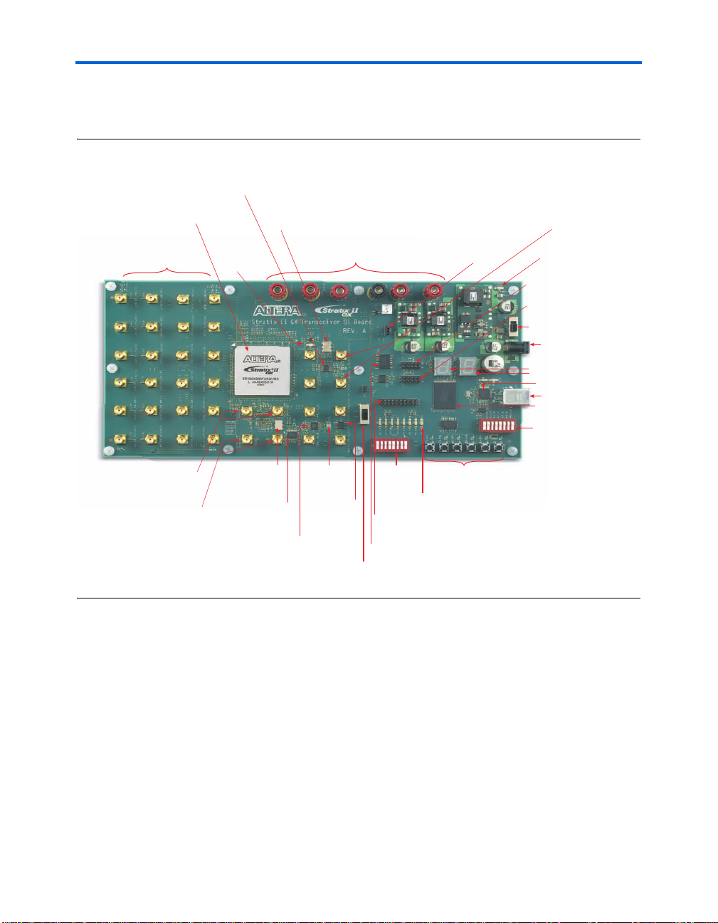
Figure 2–1 shows the Stratix II GX EP2SGX90 transceiver signal integrity
development board.
Figure 2–1. Stratix II GX Transceiver Signal Integrity Development Board
Temperature Sensor
with Alarm (U17)
Stratix II GX Device (U20)
SMA Transmit &
Receive Connectors
(J26 through J49)
SMA Output Clock Connectors
Reference Clock for Quad 1
Transceivers (J7, J8)
SMA Output Clock Connectors
Reference Clock for Quad 3
Transceivers (J9, J10)
Configuration
Done LED (D14)
156.25-MHz
Oscillator (U9)
50-MHz Oscillator
Used for System Clock (U10)
Optional Power Input
Connection Jacks (J15, J17-21)
25-MHz
Crystal (U6)
Differential
Fan-out
Buffer (U8)
Differential to
Single-Ended
Buffer (U7)
Clock
Generator (U5)
Switch (S9)
Clock
Setting
DIP Switch
Bank (S8)
Debug
Header (J1)
EPCS64 Device (U22)
Slide
Jumper Header for
VCCH Voltage (J50)
User Push-Button
Switches (S1 through S6)
User LEDs
(D1 through D8)
Getting Started
SMA Input Clock
Connectors for FPGA (J12, J14)
Power LED (D13)
10-pin Configuration Header
for EPCS64 Device (J23)
10-pin JTAG Configuration
Header for FPGA (J24)
Power Switch (S10)
Power Supply Input
Dual 7-Segment
Displays (D9, D10)
USB Interface (U2)
USB Connector (J2)
16 Mbytes Flash
Memory (U19)
User DIP Switch
Bank (S7)
f Refer to the Stratix II GX EP2SGX90 Transceiver Signal Integrity
Development Board Reference Manual (available on the Transceiver SI
Development Kit, Stratix II GX Edition CD-ROM) for information on the
board’s components.
Hardware Requirements
All of the hardware that you need to use the board is provided with the
Transceiver Signal Integrity Development Kit, Stratix II GX Edition.
Altera Corporation Getting Started User Guide 2–3
June 2006 Transceiver Signal Integrity Development Kit, Stratix II GX Edition
Page 12

Before You Begin
Software Requirements
To use the kit’s demo application, you must be running Windows XP.
Install the following software before you begin developing designs for
the kit:
■ The Quartus II software version 6.0. See “Installing the Quartus II
Software and MegaCore Functions” on page 2–7.
■ Internet Explorer 4.01 with Service Pack 2 or later to use Quartus II
Help. You need a web browser to register the Quartus II software and
request license files.
To license the Quartus II software, you will need:
■ Your network identification card (NIC) ID.
■ The kit’s serial number, which is adhered to both the outside of the
development kit’s box and the CD-ROM.
1 Your NIC ID is a 12-digit hexadecimal number that identifies
your computer. Networked (or floating-node) licensing requires
a NIC ID or server host ID. When obtaining a license file for
network licensing, you should use the NIC ID from the
computer that will issue the Quartus II licenses to distributed
users over a network. You can find the NIC ID for your card by
typing "ipconfig /all" at a command prompt. Your NIC ID
is the number on the physical address line, without the dashes.
Quartus II System Requirements
To use the Transceiver SI Development Kit, Stratix II GX Edition CD-ROM
with the Quartus II software provided with the kit, your system must
meet the Quartus II software minimum requirements.
f For system requirements, refer to the Quartus II Installation & Licensing
for PCs at www.altera.com.
2–4 Getting Started User Guide Altera Corporation
Transceiver Signal Integrity Development Kit, Stratix II GX Edition June 2006
Page 13

Getting Started
Software Installation
The instructions in this section explain how to install the following:
■ Transceiver SI Development Kit, Stratix II GX Edition CD-ROM
■ Transceiver SI Development Kit, Stratix II GX Edition demo
application and drivers
■ The Quartus II Software, Development Kit Edition, including
MegaCore functions from the MegaCore IP Library CD-ROM
Installing the Transceiver SI Development Kit, Stratix II GX Edition CD-ROM Contents
The Transceiver SI Development Kit, Stratix II GX Edition CD-ROM contains
the following items:
■ Transceiver SI Development Kit, Stratix II GX Edition GUI
application and drivers
■ Example design programming files
■ Transceiver SI Development Kit, Stratix II GX Edition Getting Started
User Guide (this document)
■ Stratix II GX EP2SGX90 Transceiver Signal Integrity Development Board
Reference Manual
1 Before you can compile the reference design, you must install
the MegaCore IP Library CD-ROM.
To ins t all t h e Transceiver SI Development Kit, Stratix II GX Edition
CD-ROM, perform the following steps:
Insert the Transceiver SI Development Kit, Stratix II GX Edition CD-ROM
into your CD-ROM drive and double click the SIIGX_SI_Kit-v1.0.0 file.
Follow the online instructions to complete the installation process.
The installation program copies the Transceiver SI Development Kit,
Stratix II GX Edition files to your hard-disk, installs the software driver
and application, and creates an icon in Programs > Altera > Stratix II GX
Signal Integrity Kit v1.0.0 (Windows Start menu), which you can use to
launch the Windows development kit GUI.
When the installation is complete, the Transceiver SI Development Kit,
Stratix II GX Edition installation program creates the directory structure
shown in Figure 2–2, where <path> is the Transceiver SI Development Kit,
Stratix II GX Edition installation directory.
Altera Corporation Getting Started User Guide 2–5
June 2006 Transceiver Signal Integrity Development Kit, Stratix II GX Edition
Page 14

Software Installation
Figure 2–2. Transceiver SI Development Kit Installed Directory Structure
<path>
The default Windows installation directory is C:\Altera\kits.
SIIGX_SI_ Kit-v1.0.0
Board_Design_Files
Docs
Examples
Table 2–1 lists the file directory names and a description of their
contents.
Table 2–1. Installed File Directory Names and Description of Contents
Directory Name Description of Contents
Board_Design_Files Contains the board design and production test files. You can use the board design
files as a starting point for creating your own prototype board.
Docs Contains the documentation related to the development kit.
Examples Contains the example design files including open-source HDL, Quartus II synthesis
and simulation files for the Transceiver SI Development Kit, Stratix II GX Edition.
Installing the Transceiver SI Development Kit, Stratix II GX Edition Demo Application and Drivers
This section explains how to download and install the kit’s demo
application and drivers.
1 If you receive an “Application Error” message when
launching the demo application, please install version 1.1 or
later versions of the .NET framework. Some Windows versions
do not have runtime DLL for the .NET application. The .NET
framework application can be downloaded from the following
link:
http://www.microsoft.com/downloads/details.aspx?FamilyId
=262D25E3-F589-4842-8157-034D1E7CF3A3&displaylang=en
■ Demo Application — Download the demo application,
StratixIIGX_GUI.exe, to a location on your hard drive.
■ Virtual COM Port (VCP) Driver — For VCP driver installation
instructions, go to the Future Technology Devices International
(FTDI) web site (www.ftdichip.com) and search for the appropriate
version of either the FT2232C or FT2232L device driver. The
2–6 Getting Started User Guide Altera Corporation
Transceiver Signal Integrity Development Kit, Stratix II GX Edition June 2006
Page 15

Getting Started
appropriate version depends on the operating system that you are
using. For example, Windows XP users need either the 1.0.2176 or the
latest version.
■ Demo Driver — For demo driver installation instructions, go to the
FTDI web site (www.ftdichip.com) and search for the appropriate
instructions based on the operating system that you are using.
Installing the Quartus II Software and MegaCore Functions
Refer to Installing the Quartus II Software in the Quartus II Installation &
Licensing Manual for PCs for software installation instructions. After
installing the software, request and install a license to enable it.
f For information on obtaining a license file, refer to “Licensing
Considerations”.
To use the Quartus II software included with the kit, you must first obtain
a license file. A one year Quartus II DKE software license is included with
the kit.
1 During the installation of the Quartus II software, you are given
the option to install the MegaCore IP Library. When prompted
to do so, choose to install the MegaCore IP Library and follow
the on-screen instructions.
Licensing Considerations
Altera Corporation Getting Started User Guide 2–7
June 2006 Transceiver Signal Integrity Development Kit, Stratix II GX Edition
Before using the Quartus II software, you must request a license file from
the Altera web site at www.altera.com/licensing and install it on your
computer. When you request a license file, Altera emails you a license.dat
file that enables the software.
To obtain a license, perform the following steps.
1. Point your web browser to the Altera web site at
www.altera.com/licensing.
2. In the Development Kit Licensing list, select Licensing for RoHS
Compliant Development Kits.
3. Follow the on-line instructions to request your license. A license file
is emailed to you.
1 Before installing your license, close the following software if it is
running on your computer:
● The Quartus II software
● The MAX+PLUS
®
II software
Page 16

Connect the Cables to the Board and Computer
Connect the
Cables to the
Board and
Computer
● The LeonardoSpectrum
● The Synplify software
● The ModelSim
● The Precision RTL Synthesis Software
4. To install your license, refer to Specifying the License File in the
Quartus II Installation & Licensing Manual for PCs, which is included
with the kit.
The instructions in this section explain how to set up the following
hardware:
■ USB-Blaster download cable
■ SMA cable
■ Power supply cable
®
simulator
™
synthesis tool
USB-Blaster Cable
Connect the USB-Blaster cable’s 10-pin female plug to the Stratix II GX
device’s JTAG header on the Stratix II GX EP2SGX90 transceiver signal
integrity development board (J24), and connect the other end to the USB
port on your computer. This approach allows you to directly configure
the Stratix II GX device using an SRAM Object File (.sof). The kit’s
reference design includes a SOF for directly configuring the Stratix II GX
device.
When connecting the JTAG side of the USB-Blaster cable, connect the
marker line on the cable to pin 1 of the header (J24). Pin 1 of J24 is
numbered on the board.
1 The USB-Blaster download cable driver must be installed before
the USB-Blaster download cable can be used.
f For information about installing the USB-Blaster download cable driver
included with the Quartus II software, refer to the USB-Blaster Download
Cable User Guide. The driver files are installed at <quartus-install-dir>
\drivers\usb-blaster.
SMA Cable
The ends of the SMA cable can be connected to the SMA clock input
connector.
2–8 Getting Started User Guide Altera Corporation
Transceiver Signal Integrity Development Kit, Stratix II GX Edition June 2006
Page 17

Getting Started
Power Supply Cable
Connect the power cable to the board and plug the other end into a power
outlet. To power up the board, place the power switch (S10) in the ON
position. When power is supplied to the board, the LED (D13)
illuminates.
After the board powers up, the on-board flash memory, which ships
pre-programmed with the factory design, automatically configures the
Stratix II GX device. The CONF DONE LED (D14) illuminates, signaling
that the Stratix II GX device is configured.
1 If the board does not power up after the power cable is
connected, make sure that the power switch (S10) is in the ON
position.
Setting the Clock
Set the DIP switch S8 and slide switch S9 per the instructions listed in
Table 2–2.
Circuit Switches
Table 2–2. Setting the Clock Circuit Switches, Note (1)
S8-1, S8-2, and PCIe Clk S8-3, S8-4 and PCIe Clk S8-5 and PCIe Clk S8-6 and Basic Clk
S8-1 S8-2
Low Low 25 MHz Low Low ±25% High Enable High Enable
High Low 100 MHz High Low -0.5% Low Disable Low Disable
Low High 125 MHz Low High -0.75% ————
High Low 200 MHz High High No
Note to Ta b le 2 –2 :
(1) When using the clock speed DIP switch bank (S8), set switches 1-5, 7, and 8 in the closed position, and switch 6 in
the open position.
PCIe Clk
(U5)
S8-3 S8-4
1 To use the on board oscillator, the slide switch (S9) needs to be in the OSC
position. However, to use the SMA connectors J5 and J6, the slide switch
needs to be in the SMA position. The I/O standard of the pattern generator
should be set to LVPECL, LVDS, LVHSTL, SSTL, or the HCSL level.
PCIe Clk
(U5)
spread
S8-5
————
PCIe Clk
(U5)
S8-6
Basic Clk
(U8)
Altera Corporation Getting Started User Guide 2–9
June 2006 Transceiver Signal Integrity Development Kit, Stratix II GX Edition
Page 18

Test the Transceiver Performance Using Pre-Defined Designs
Test the
Transcei ver
Performance
Using
Pre-Defined
Designs
The kit provides pre-defined test designs and an easy-to-use demo
application with a custom graphical user interface (GUI). The demo
application’s GUI allows extensive transceiver channel testing at various
data rates and clocking schemes.
This section provides:
■ Pre-defined test design results
■ Demo application GUI tutorial
Pre-Defined Test Designs
Altera engineers created a set of pre-defined test designs for you to
evaluate Stratix II GX device transceiver performance and board features.
As you can tell from the data listed in Table 2–3, the results can vary
dramatically when choosing from various clocking schemes and data
rates.
Table 2–3 lists the default transceiver settings.
Table 2–3. Transceiver Test Design Results
File Name
gxbguictrl_top1.sof 6.25 3.125 6.25 Clock from
gxbguictrl_top2.sof 5 2.5 5 Clock from
Note to Ta b le 2 –3 :
(1) The clock input can also be given from an external source. The frequency of the clock should be selected such that
the data rate in Quads 1 and 3 should be within the 6.375 Gbps - 3.126 Gbps range. For Quad2 the data rate should
be within the 3.125 Gbps-622 Mbps range. See Ta b le 2 –4 .
Quad 1 Channel 1
Data Rate (Gbps)
Quad 2 Channel 1
Data Rate (Gbps)
Quad 3 Channel 1
Data Rate (Gbps)
Clocking Scheme
Note (1)
156.25-MHz
oscillator
156.25-MHz
oscillator
f Refer to the section “Connect the Cables to the Board and Computer” on
page 2–8 for information on using the JTAG interface when configuring
the Stratix II GX device with one of the pre-defined designs. The
CONF DONE LED (D14) illuminates upon successful device
configuration. Also, the 7-segment display shows the programmed
SOF/POF number. For example, for the gxbguictrl_top1.sof the
7-segment display indicates the SOF with 01, and with the
gxbguictrl_top2.sof the 7-segment display indicates the SOF with 02.
2–10 Getting Started User Guide Altera Corporation
Transceiver Signal Integrity Development Kit, Stratix II GX Edition June 2006
Page 19

Getting Started
Table 2–4 lists the allowed input clock frequency range for the various
GUI channels.
Table 2–4. Input Clock Frequency Range for GUI Channels
GUI Channel
Number
Ch0, Ch5 6.375 Gbps – 3.126 Gbps 159.375 MHz – 78.15 MHz
Ch1..Ch4 3.125 Gbps – 622 Mbps 156.25 MHz – 62 MHz
Data Rate Range Clock Frequency Range
Demo Application GUI Tutorial
The demo application’s GUI provides an easy-to-use control panel where
you can select various transceiver settings and observe the results. This
feature allows you to customize your board design by choosing
transceiver settings from the following categories (see Figure 2–3):
■ Analog
■ Communication cable
■ Data patterns
■ Serial loopback
■ Resets
■ Clock recovery unit (CRU)
■ Link control
To execute the demo application’s GUI, double-click the
StratixIIGX_GUI.exe file, which is available on the Transceiver SI
Development Kit, Stratix II GX Edition CD-ROM.
Altera Corporation Getting Started User Guide 2–11
June 2006 Transceiver Signal Integrity Development Kit, Stratix II GX Edition
Page 20

Test the Transceiver Performance Using Pre-Defined Designs
Figure 2–3. Demo Application Control Panel WIndow
1 Before walking through the GUI tutorial, you should configure
the Stratix II GX device with one of the pre-defined SOFs listed
in Ta bl e 2 – 3.
Analog Settings
The left side of the control panel window provides the physical media
attachment sublayer (PMA) setting values that represent the different
transceiver Quads and are based on the VCCHTX setting. The VCCHTX
setting should correspond with jumper header (J50) settings. See
Table 2–5.
Table 2–5. Jumper Header (J50) Connections and VCCHTX Values
Jumper Header (J50) Connection VCCHTX
Pins 1 and 2 1.5 V
Pins 2 and 3 1.2 V
2–12 Getting Started User Guide Altera Corporation
Transceiver Signal Integrity Development Kit, Stratix II GX Edition June 2006
Page 21

Figure 2–4 shows the jumper header connections and corresponding
VCCHTX values.
Figure 2–4. Jumper Header Connections and Corresponding VCCHTX Values
3V3
C52
10µF 0805
U15
7
IN
8
S/D
1
ADJ
GND02
GND01
BIAS
BACK
94
5
5V
3
2
OUT
8
NC
LP38842MR-ADJ
R46
10K
(1%)
C44
0.1µF
R45
16.9K
(1%)
C54
130pF
J50
CONN_3
123
R44
11.5K
(1%)
VCCHTX
F6
C53
200pF
Getting Started
J20
BANANA_JACK_RED
Red
+
C49
4.7µF Tantalum
1 Before powering up the board, the VCCHTX jumper settings
should be specified.
The following list defines the analog setting parameters in the control
panel window:
■ VOD = output driver voltage
■ EQ = equalization
■ Gain = DC gain
■ PE = pre-emphasis
● In the PE setting list, Pre, 1
st
Post, and 2nd Post settings represent
different taps.
■ PDN = Setting the PDN performs a power down on the Quad.
Communication Settings
The top right-hand side of the control panel window provides the
following Communication settings:
■ Communication Cable—This list displays the different physical
interconnect options to communicate with the board. Currently, USB
Serial is supported.
Altera Corporation Getting Started User Guide 2–13
June 2006 Transceiver Signal Integrity Development Kit, Stratix II GX Edition
Page 22

Test the Transceiver Performance Using Pre-Defined Designs
■ COM Port #—When the driver is installed, the COM Port values are
listed under Ports (COM and LPT) in the Windows Device Manager
window (go to Start > Control Panel > Administrative Tools >
Computer Management > Device Manager). See Figure 2–5. The
highest COM port number listed under Ports (COM and LPT) is
required to be used in the COM Port # box.
■ Open Link and Close Link—When you click Open Link or Close
Link, the link with the board and the status of the connection is
shown under Display Adapters in the Device Manager window (see
Figure 2–5).
Figure 2–5. Device Manager Window
1 When the SOF is downloaded to the hardware, the link from the
GUI to the board should be closed.
Data Pattern Settings
The top center of the control panel window provides the following Data
Pattern settings:
■ Ch0 Pattern
■ Ch1., Ch4 Pattern
■ Ch5 Pattern
2–14 Getting Started User Guide Altera Corporation
Transceiver Signal Integrity Development Kit, Stratix II GX Edition June 2006
Page 23

Getting Started
Three different data pattern generators—PRBS7, PRBS23, and high
frequency alternate 1s and 0s—are available for all channels. Data
checking is only available for the PRBS7 and PRBS23 pattern generators.
Error statistics are reported to the demo application by the checkers.
Serial Loopback Settings
Immediately to the right of the Data Pattern settings are the Serial
Loopback settings. Serial loopback is available for all the channels and
can be controlled during run time.
1 After the serial loopback status in the GUI is changed, the Data
Chk Status box may indicate Unsync’d for some channels due
to the asynchronous nature of the serial loopback signal. In this
scenario, the Data Pat Rst should be asserted to synchronize the
error checker with the transmitted data.
Reset Settings
Immediately to the right of the Serial Loopback settings are the Reset
settings, which are defined below:
■ System Rst—Reset for the transceiver
1 After System Rst is asserted, the Data Chk Status box may
show Unsync’d for some channels due to the asynchronous
nature of the reset. In this scenario, the Data Pat Rst should be
asserted to synchronize the error checker with the transmitted
data.
■ Error Cnt Rst—Reset for all the error counters to zero
■ SIIGX Temp—This field shows the Stratix II GX device’s junction
temperature.
1 Also, when the you change the data patterns in the Data
Patterns field (depending on the specified channel), the error
counters will be reset. For example, in the Ch1.,Ch4 Pattern
field, if you change PRBS7 to PRBS23, the error counters are
reset for all four channels.
RX CRU Rx_Freqlocked Lock to Settings
The middle center of the control panel window is the RX CRU
rx_freqlocked Lock to: settings. This field shows whether the
transceiver’s CRU is locked to the reference clock or to the data. When the
Altera Corporation Getting Started User Guide 2–15
June 2006 Transceiver Signal Integrity Development Kit, Stratix II GX Edition
Page 24

Test the Transceiver Performance Using Pre-Defined Designs
transceiver locks to the incoming data, the RX CRU rx_freqlocked Lock
to: field displays Data indicating that the receiving PLL has recovered the
clock from the incoming data.
Link Control Settings
The bottom center of the control panel window provides the Link
Control settings. The Link Control settings include the following options:
■ Using SMA Clock—When the Using SMA Clock field is selected,
the serial data rate is shown as a multiplication factor of the clock
frequency for all channels. The multiplication factor is based on the
channel width used in the test design. When the external clock is
used to run the transceiver, the P and N differential outputs of the
clock source should be connected to SMA connectors J5 and J6
respectively and switch S9 should be set to the SMA position.
■ What statistic to display?—This list displays the bit error rate,
number of bits received, number of errors received, and error rate
slope. The error rate slope provides an approximate indication of the
increasing and decreasing trend of the number of errors received.
■ Inject Error—This button injects errors in the channels. Every time
this button is asserted, a one bit error is introduced.
■ Data Pat Rst—Reset for the data pattern generators and checkers.
■ Data Rate—Based on the selected test design, the Data Rate box
displays the serial data rate of the transceiver channels.
■ GXB Encoding—The GXB Encoding box displays whether the data
sent by the test design is 8B/10B encoded.
Data Chk Status—Before transmitting the data patterns, the pattern
generators transmit a pre-defined header byte to enable the error
checkers. Upon receiving the pre-defined header byte, the error checker
monitors for errors in the received pattern. The Data Chk Status box
displays the following:
● Sync’d status displayed in green indicates that the error checker
has received the pre-defined header byte and no errors are
detected.
● Unsync’d status displayed in gray indicates that the error
checker has not received the pre-defined header byte. When this
situation occurs, you should ensure that the transmitter of the
channel showing Unsync’d is connected to the receiver channel
by external cable or by internal serial loopback. Still, when
2–16 Getting Started User Guide Altera Corporation
Transceiver Signal Integrity Development Kit, Stratix II GX Edition June 2006
Page 25

Getting Started
sending a high frequency data pattern, the Data Chk Status box
will also show Unsync’d. This is because the error checker does
not monitor for high frequency error data patterns.
● Error status indicates that the error checker is detecting errors in
the received pattern.
■ Freeze Display—When the Freeze Display button is pressed, the
display field is not changed. However the counting is not stopped.
When the Unfreeze Display is pressed, the current running values
are shown.
Measuring Signal Eye Diagrams of Transmitted Data
f For information on using Altera megafunctions to customize transceiver
The on-board EP2SGX90E device’s embedded transceivers support up to
12 transceiver channels. Each transceiver channel has a transmitter and a
receiver. Designers can preset Stratix II GX transceiver functions using
the Quartus II software.
Stratix II GX devices are designed with superior pre-emphasis and
equalization. Pre-emphasis conditions the signal prior to transmission
resulting in an open eye at the far end, while equalization opens the eye
in the receiver. Pre-emphasis and equalization ensure optimal signal
integrity.
In this section, you will walk through the process of measuring signal eye
diagrams of transmitted data.
The following lists the required test equipment:
■ Sampling oscilloscope with Infinite Persistence display capability,
such as Tektronix TDS8000
■ Two length matched 50-Ω SMA cables for transmission data out
(TX_Px and TX_Nx) with at least 18GHZ bandwidth.
■ One 50-ohm SMA cable for the Trigger input to the oscilloscope.
channels, refer to the Stratix II GX alt2gxb Megafunction User Guide
chapter of the Stratix II GX Device Handbook, Volume 2.
Set Up The Testing Environment
This section provides the steps in setting up a testing environment.
Depending on the design running on the development board, one or
more of the six transmitter channels will transmit serial data.
Assuming the design is successfully running on the Stratix II GX
transceiver signal integrity board, the following steps walk you through
the process of measuring eye-diagrams of transmitted data.
Altera Corporation Getting Started User Guide 2–17
June 2006 Transceiver Signal Integrity Development Kit, Stratix II GX Edition
Page 26

Measuring Signal Eye Diagrams of Transmitted Data
1. Connect a 50-Ω SMA cable between the TX_P0 through TX_P5
connectors on the board (depending on the channel for which the
eye-diagram needs to be measured) and Ch1 on the TDS8000
sampling module.
1 The TX_P5 channel has a 40 inch trace between the FPGA
serial data output pin and the SMA connector.
2. Connect an equal length 50-Ω SMA cable between the TX_N0 and
TX_N5 connectors on the board and Ch2 on the TDS8000 sampling
module.
1 The TX_N5 channel has a 40 inch trace between the FPGA
serial data output pin and the SMA connector.
3. Connect a 50-Ω SMA cable between the clock trigger output (J3 or J4
depending on which clock is specified as the design’s refclk) and
the direct trigger input on the TDS8000 front panel.
4. Customize the TDS8000 to measure the eye diagram on differential
data streams. You can do this by using the math utility provided on
the sampling oscilloscope. Setting up the math utility to measure
eye diagrams on Ch1-Ch2 effectively gives a differential eye
measurement (See Figure 2–6).
1 Use the DC block for high-speed signals going into the
oscilloscope, e.g., TX_P0, and TX_N0. For the trigger clock
output from the Stratix II GX transceiver signal integrity board,
use the DC block. Also use the attenuator depending on the
allowable input voltage range of the oscilloscope.
2–18 Getting Started User Guide Altera Corporation
Transceiver Signal Integrity Development Kit, Stratix II GX Edition June 2006
Page 27

Figure 2–6. Connecting the TDS8000 Sampling Oscilloscope
TX_P0
TX_N0
Getting Started
TDS 8000 Sampling Scope
Basic_trig_clock
f For more information, please refer to the Tektronix TDS8000 User Guide or
reference manual of the sampling oscilloscope used.
Altera Corporation Getting Started User Guide 2–19
June 2006 Transceiver Signal Integrity Development Kit, Stratix II GX Edition
Page 28

Measuring Signal Eye Diagrams of Transmitted Data
2–20 Getting Started User Guide Altera Corporation
Transceiver Signal Integrity Development Kit, Stratix II GX Edition June 2006
Page 29

Appendix A. Non-GUI Based
Example Design
Design Features
This manually-controlled (non-GUI based) example is a one channel
design using the microstrip transceiver quad at 6.25 Gbps. The input
clock frequency is 156.25 MHz and the interface is 40 bits wide. The
TX_P0 is connected to A4 and RX_P0 to C1. The other transceiver quads
that are not used are powered off. Data patterns supported are PRBS23,
PRBS7, and the high frequency pattern (1010).
1 The checkers are only available for the PRBS23 and PRBS7 data
patterns.
The following parameters can be controlled during run-time:
■ Preemphasis—Main tap (The other tap controls are not available.)
■ Equalization
■ DC gain
■ VOD
■ Data pattern select
■ Serial loopback
The parameters are controlled using a combination of DIP switches and
push-button switches. See Tab l e A –1 . The on-board frequency rate used
for the design is 156.25 MHz. Please set switch 6 in the clock setting DIP
switch bank (S8) to OPEN. Figure A–1 shows all the switches in the closed
position.
Figure A–1. Clock Setting DIP Switch Bank (All Switches In Closed Position)
Altera Corporation Getting Started User Guide A–1
June 2006 Transceiver Signal Integrity Development Kit, Stratix II GX Edition
Page 30

General User Interfaces
General User
This section describes the following general user interfaces, which
provide direct feedback regarding board, clocking, and signal activity:
Interfaces
■ LED display
■ 7-segment display
■ DIP switches
■ Push buttons
LED Display
Signals propagating to LEDs indicate board status. Ta bl e A – 1 lists the
signal name, description, width, board reference number, and the FPGA
pin in which the signal is connected.
Table A–1. LED Display (Part 1 of 2)
Number Signal Name Description Width
1 Tx_pll_locked Shows whether the TX phase-locked
loop (PLL) is locked to the input clock
2 Rx_syncstatus When ON, indicates that the receiver
has acquired synchronization with the
input data.
3 Checker_synced Indicates that the checker is checking
for errors on the received data.
4 Error_flag The LED is ON for one second when
an error is detected by the pattern
checker. Shows the running error
status.
5 Error
status_first_digit
(1)
6 Error
status_second_digit
(1)
7 Error
status_third_digit
(1)
The LED is ON if the LSB[7:0] of the
error counter reaches 0xFF. The LED
is reset when
clear_error_counter_switch is
asserted.
The LED is ON if the LSB[15:8]of
the error counter reaches 0xFF. The
LED is reset when
clear_error_counter_switch is
asserted.
The LED is on if the LSB[23:16] of
the error counter reaches 0xFF. The
LED is reset when
clear_error_counter_switch is
asserted.
1D1 AE33
1D2 AE32
1D3 AD26
1D4 AD25
1D5 AD34
1D6 AE34
1D7 AC29
Board
Reference
Number
Connected
to FPGA Pin
Number
A–2 Getting Started User Guide Altera Corporation
Transceiver Signal Integrity Development Kit, Stratix II GX Edition June 2006
Page 31

Table A–1. LED Display (Part 2 of 2)
Number Signal Name Description Width
8 Serial_loopback The LED is ON when serial loopback
is enabled
Note to Ta b le A –1 :
(1) The first, second, and third digits display the approximate error count range.
1D8 AC28
7-Segment Display
The 7-segment displays are used to:
■ Display the VOD, pre-emphasis, DC gain, and equalization values
when reading or writing the PMA settings.
f Refer to the “Write and Read PMA values” on page A–6 for more
information.
■ Display the design file name when the system_reset push button
switch is asserted.
■ Display the error count when show_error_count push button
switch is asserted.
1 The VOD values shown by the 7-segment display indicates the
value in mV when multiplied by 100. For example, to show a
VOD of 200mV the 7-segment display shows 02. The display
setting is for a VCCHTX of 1.5 V.
Board
Reference
Number
Connected
to FPGA Pin
Number
DIP Switches
The DIP switch S7 is used for controlling the different transceiver
parameters. Ta bl e A –2 lists the DIP switch names and describes the
individual switch functions. The DIP switch numbers are shown on the
board’s silkscreen.
Altera Corporation Getting Started User Guide A–3
June 2006 Transceiver Signal Integrity Development Kit, Stratix II GX Edition
Page 32

General User Interfaces
1 To set a DIP switch in the open position, press the switch
towards the OPEN side of the user DIP switch bank. To set a DIP
switch in the closed position, press the switch towards the
number side of the DIP switch bank.
Table A–2. DIP Switch Signal Names and Descriptions Note (1)
Board
DIP Switch Name Description Width
Reference
Number
Read and write PMA
control
PMA controls Silkscreen number:
Data pattern select The switch selects the data patterns.
Serial loopback The switch dynamically controls serial
Reserved — 1 8 AG28
The switch is used to display or set the
controllable parameters. The values are
displayed in the 7-segment display, i.e.,
O = read VOD, preemphasis from the
transceiver
C = write VOD, preemphasis into the
transceiver
4 3 2
O O O – preemphasis (only main tap)
O O C – VOD
O C C – DC gain
C C C – equalization
The other silkscreen numbers are reserved.
After this combination is set,
push_button_PMA_control has to be
pressed to set the values.
Switch position-silkscreen number:
6 5
C O – PRBS23
O C – PRBS7
O O – high frequency
C C – reserved
loopback.
O = serial loopback ON
C = serial loopback OFF
11 AH33
3 2, 3, 4 AH32,
25, 6 AJ34,
17 AG29
Connected
to FPGA Pin
Number
AF28,
AF27
AJ33
Note to Table A-2:
(1) The C refers to the DIP switch in the closed position, and the O refers to the DIP switch in the open position.
A–4 Getting Started User Guide Altera Corporation
Transceiver Signal Integrity Development Kit, Stratix II GX Edition June 2006
Page 33

Push Button Switches
Ta bl e A –3 lists the push button switch signal names, describes the
functionality, lists the board reference numbers, and FPGA pin
connection.
Table A–3. Push Button Switches
Board
Push Button Switch Name Description
Reference
Number
resetn (system reset) Performs a reset on the transceiver and
also the entire design.
generator_checker_reset_switch Performs a reset on the data generators
and error checkers. The push button will
also reset the error counters.
change_PMA_switch Based on the selection of the PMA
Controls DIP switch, the push button sets
the value for either VOD, preemphasis,
DC gain or equalization.
Every time the push button is pressed, the
value is incremented. When the
maximum value is reached, the value
starts from zero.
insert_error_switch Inserts one bit error in the transmit data. S4 AE30
clear_error_counter_switch The push button resets the error
counters.
show error count Displays the most significant byte of the
error. For example if the error count is
02FF, when the push button is asserted
02 is displayed until the button is
de-asserted. Refer to Table A–1 on
page A–2 for additional information.
S1 AD28
S2 AF34
S3 AF33
S5 AE29
S6 AH20
Connected
to FPGA
Number
Pin
Altera Corporation Getting Started User Guide A–5
June 2006 Transceiver Signal Integrity Development Kit, Stratix II GX Edition
Page 34

Write and Read PMA Values
Write and Read
PMA Values
f Refer to “DIP Switches” on page A–3 for the values.
f Refer to the “Push Button Switches” on page A–5 for more information.
This section walks you through setting up the example design’s write and
read PMA values.
Write PMA Values
Use the following steps to set up the example design:
1. Set read_write_PMA_control (DIP_sw[0]) to the closed
position.
2. Set PMA_controls (DIP_sw[3,2,1]) DIP switch to preemphasis,
VOD, equalization, or DC gain settings.
3. Assert Change_PMA_switch push button switch (S3) to change the
value of selected PMA_control.
4. Observe the values in the 7-segment display. The value written in
the transceiver is displayed.
1 The VOD values shown by the 7-segment display indicates the
value in mV when multiplied by 100. For example to show a
VOD of 200mV, the 7-segment display shows 02. This display
setting is for a VCCHTX of 1.5 V.
Read PMA Values
Use the following steps to set up the example design:
1. Set read_write_PMA_control (DIP_sw[0]) to the open position.
2. Set PMA_controls (DIP_sw[3,2,1]) DIP switch to preemphasis,
VOD, equalization, or DC gain settings.
f Refer to “DIP Switches” on page A–3 for the values.
3. Observe the values in the 7-segment display. The value read from
the transceiver is displayed.
A–6 Getting Started User Guide Altera Corporation
Transceiver Signal Integrity Development Kit, Stratix II GX Edition June 2006
Page 35

Design Walkthrough
This section walks you through a design example and also provides
troubleshooting and debugging solutions.
With
Troubleshooting
and Debugging
Solutions
f Refer to “Write PMA Values” on page A–6.
Design Walkthrough
The following steps walk you through an example sequence to run a
PRBS23 with the values of VOD = 2, preemphasis = 1, DC gain = 1, and
equalization = 3.
1 Please refer to “Stratix II GX Transceiver Signal Integrity
Development Board” on page 2–3 for all component number
references.
1. Power up the board.
2. If the on-board clock is used, ensure that the slide switch (S9) is in
the oscillator position (OSC).
3. Set switch 6 of the clock setting DIP switch bank (S8) to OPEN.
4. Set switch 7 of the user DIP switch bank (S7) to OPEN for serial
loopback.
5. To set the pattern generator to PRBS23, set switch 6 of the user DIP
switch bank (S7) to closed and switch 5 to OPEN.
6. Set the VOD, preemphasis, DC gain, and equalization values.
7. This is an optional step. Refer to “Read PMA Values” on page A–6
to confirm whether the intended settings are written.
8. Assert the push button switch S2 to reset the data generators and
checkers.
9. Check the status of LED’s D1, D2, and D3. When all three LEDs are
illuminated, the transaction is successful.
Altera Corporation Getting Started User Guide A–7
June 2006 Transceiver Signal Integrity Development Kit, Stratix II GX Edition
Page 36

Design Walkthrough With Troubleshooting and Debugging Solutions
Troubleshooting Solutions
This section provides troubleshooting solutions. If your transaction is not
successful, review the following troubleshooting suggestions:
■ If the LED D1 is not illuminated, the system may not be receiving the
clock cycles. Ensure that the slide switch (S9) is in the oscillator
position (OSC). Also, ensure that switch 6 of the clock setting DIP
switch bank (S8) is set to OPEN.
■ If the LED D2 is not illuminated, the receiver cannot sync to the
transmitted data. To remedy this problem:
● Ensure that serial loopback is ON if external loopback is not
completed.
● If external loopback is completed, check the quality of the cables
used.
● Assert the system_reset push button switch.
■ If the LED D3 is not ON, the data checker did not receive the
expected data. To remedy this problem:
● Ensure that the data pattern of the DIP switch is set to PRBS7 or
PRBS23.
1 High frequency data patterns do not have a data checker.
Therefore, the LED D3 will be off when high frequency patterns
are used.
■ If the display shows EE, the DIP switch selection for PMA_controls
is not correct.
Debugging Using the SignalTap® II Embedded Logic Analyzer
In the kit’s Examples\SII_GX_SI_NonGUI_Design directory there is a
Quartus®II archive (.qar) file containing the example design project. The
design1.stp file is part of the .qar file and contains a variety of debugging
signals. The available signals are:
■ All resets going into the transceivers
■ Status signals from transceivers: rx_freqlocked,
rx_syncstatus
■ Input push button and DIP switch values
■ Reconfiguration block signals
● Inputs and outputs of VOD, preemphasis, equalization and DC
gain values
● Read, write, busy, and data valid signals
■ Data generator and checker signals
● Parallel data output to the transceiver
A–8 Getting Started User Guide Altera Corporation
Transceiver Signal Integrity Development Kit, Stratix II GX Edition June 2006
Page 37

● Data pattern selected by the DIP switch, which have the
following values:
• 01: PRBS23
• 10: PRBS7
• High frequency pattern (1010)
● Receive side data to PRBS23 and PRBS7 checkers.
● Error count values for PRBS23 and PRBS7 checkers
● Lock signals for PRBS23 and PRBS7 checkers. This indicates that
the checker matched the receive pattern with the expected data
pattern.
Creating Your Custom Data Generators and Checkers
The data_gen_checker_top_40bits.v is the top level for the data
generators and checkers. If you would like to create your own data
generators and checkers, replace this module with your own module. The
data output of this module should be connected to the tx_datain port
of the transceiver instantiation (alt2gxb_6G_6250.v) in the top-level
design_s2gx_top_level.v.
Altera Corporation Getting Started User Guide A–9
June 2006 Transceiver Signal Integrity Development Kit, Stratix II GX Edition
Page 38

Creating Your Custom Data Generators and Checkers
A–10 Getting Started User Guide Altera Corporation
Transceiver Signal Integrity Development Kit, Stratix II GX Edition June 2006
 Loading...