

Page 1

Altera Transceiver PHY IP Core User
Guide
Subscribe
Send Feedback
UG-01080
2015.01.12
101 Innovation Drive
San Jose, CA 95134
www.altera.com
Page 2

TOC-2
Altera Transceiver PHY IP Core User Guide
Contents
Introduction to the Protocol-Specific and Native Transceiver PHYs............... 1-1
Getting Started Overview....................................................................................2-1
Protocol-Specific Transceiver PHYs.........................................................................................................1-1
Native Transceiver PHYs ...........................................................................................................................1-2
Non-Protocol-Specific Transceiver PHYs................................................................................................1-4
Transceiver PHY Modules..........................................................................................................................1-4
Transceiver Reconfiguration Controller...................................................................................................1-5
Resetting the Transceiver PHY..................................................................................................................1-5
Running a Simulation Testbench.............................................................................................................. 1-6
Unsupported Features.................................................................................................................................1-9
Installation and Licensing of IP Cores......................................................................................................2-1
Design Flows.................................................................................................................................................2-2
MegaWizard Plug-In Manager Flow.........................................................................................................2-3
Specifying Parameters..................................................................................................................... 2-3
Simulate the IP Core........................................................................................................................2-4
10GBASE-R PHY IP Core...................................................................................3-1
10GBASE-R PHY Release Information.................................................................................................... 3-6
10GBASE-R PHY Device Family Support................................................................................................3-6
10GBASE-R PHY Performance and Resource Utilization for Stratix IV Devices..............................3-7
10GBASE-R PHY Performance and Resource Utilization for Arria V GT Devices.......................... 3-7
10GBASE-R PHY Performance and Resource Utilization for Arria V GZ and Stratix V
Devices.....................................................................................................................................................3-8
Parameterizing the 10GBASE-R PHY.......................................................................................................3-8
General Option Parameters........................................................................................................................3-9
Analog Parameters for Stratix IV Devices..............................................................................................3-12
10GBASE-R PHY Interfaces.....................................................................................................................3-13
10GBASE-R PHY Data Interfaces...........................................................................................................3-14
10GBASE-R PHY Status, 1588, and PLL Reference Clock Interfaces................................................3-17
Optional Reset Control and Status Interface......................................................................................... 3-18
10GBASE-R PHY Clocks for Arria V GT Devices................................................................................3-19
10GBASE-R PHY Clocks for Arria V GZ Devices................................................................................3-20
10GBASE-R PHY Clocks for Stratix IV Devices...................................................................................3-21
10GBASE-R PHY Clocks for Stratix V Devices.....................................................................................3-22
10GBASE-R PHY Register Interface and Register Descriptions.........................................................3-23
10GBASE-R PHY Dynamic Reconfiguration for Stratix IV Devices.................................................3-28
10GBASE-R PHY Dynamic Reconfiguration for Arria V and Stratix V Devices.............................3-29
1588 Delay Requirements.........................................................................................................................3-30
10GBASE-R PHY TimeQuest Timing Constraints.............................................................................. 3-30
10GBASE-R PHY Simulation Files and Example Testbench.............................................................. 3-32
Altera Corporation
Page 3

Altera Transceiver PHY IP Core User Guide
Backplane Ethernet 10GBASE-KR PHY IP Core with Early Access FEC
Option..............................................................................................................4-1
10GBASE-KR PHY Release Information................................................................................................. 4-3
Device Family Support................................................................................................................................4-3
10GBASE-KR PHY Performance and Resource Utilization..................................................................4-3
Parameterizing the 10GBASE-KR PHY....................................................................................................4-4
10GBASE-KR Link Training Parameters .................................................................................... 4-5
10GBASE-KR Auto-Negotiation and Link Training Parameters.............................................4-7
10GBASE-R Parameters..................................................................................................................4-7
1GbE Parameters..............................................................................................................................4-9
Speed Detection Parameters.........................................................................................................4-10
PHY Analog Parameters...............................................................................................................4-10
10GBASE-KR PHY IP Core Functional Description........................................................................... 4-10
10GBASE-KR PHY Arbitration Logic Requirements...........................................................................4-14
10GBASE-KR PHY State Machine Logic Requirements......................................................................4-15
Forward Error Correction (Clause 74)................................................................................................... 4-15
10BASE-KR PHY Interfaces.....................................................................................................................4-19
10GBASE-KR PHY Clock and Reset Interfaces.................................................................................... 4-20
10GBASE-KR PHY Data Interfaces............................................................................................ 4-22
10GBASE-KR PHY Control and Status Interfaces....................................................................4-25
Daisy-Chain Interface Signals......................................................................................................4-27
Embedded Processor Interface Signals.......................................................................................4-28
Dynamic Reconfiguration Interface Signals.............................................................................. 4-29
Register Interface Signals..........................................................................................................................4-32
10GBASE-KR PHY Register Definitions................................................................................................4-32
PMA Registers............................................................................................................................................4-47
PCS Registers..............................................................................................................................................4-48
Creating a 10GBASE-KR Design.............................................................................................................4-49
Editing a 10GBASE-KR MIF File ........................................................................................................... 4-50
Design Example..........................................................................................................................................4-52
SDC Timing Constraints.......................................................................................................................... 4-53
Acronyms....................................................................................................................................................4-53
TOC-3
1G/10 Gbps Ethernet PHY IP Core.....................................................................5-1
1G/10GbE PHY Release Information....................................................................................................... 5-2
Device Family Support................................................................................................................................5-3
1G/10 GbE PHY Performance and Resource Utilization.......................................................................5-3
Parameterizing the 1G/10GbE PHY..........................................................................................................5-4
1GbE Parameters..........................................................................................................................................5-4
Speed Detection Parameters.......................................................................................................................5-5
PHY Analog Parameters.............................................................................................................................5-6
1G/10GbE PHY Interfaces..........................................................................................................................5-7
1G/10GbE PHY Clock and Reset Interfaces............................................................................................ 5-8
1G/10GbE PHY Data Interfaces................................................................................................................ 5-9
XGMII Mapping to Standard SDR XGMII Data.................................................................................. 5-11
Serial Data Interface.................................................................................................................................. 5-12
Altera Corporation
Page 4

TOC-4
Altera Transceiver PHY IP Core User Guide
1G/10GbE Control and Status Interfaces...............................................................................................5-12
Register Interface Signals..........................................................................................................................5-14
1G/10GbE PHY Register Definitions .....................................................................................................5-15
PMA Registers............................................................................................................................................5-16
PCS Registers..............................................................................................................................................5-17
1G/10 GbE GMII PCS Registers..............................................................................................................5-18
PMA Registers............................................................................................................................................5-20
1G/10GbE Dynamic Reconfiguration from 1G to 10GbE...................................................................5-21
1G/10GbE PHY Arbitration Logic Requirements.................................................................................5-22
1G/10GbE PHY State Machine Logic Requirements............................................................................5-23
Editing a 1G/10GbE MIF File ................................................................................................................. 5-23
Creating a 1G/10GbE Design...................................................................................................................5-24
Dynamic Reconfiguration Interface Signals.......................................................................................... 5-25
1G/10 Gbps Ethernet PHY IP Core.........................................................................................................5-27
Design Example..........................................................................................................................................5-29
Simulation Support....................................................................................................................................5-30
TimeQuest Timing Constraints...............................................................................................................5-30
Acronyms....................................................................................................................................................5-30
XAUI PHY IP Core............................................................................................. 6-1
XAUI PHY Release Information............................................................................................................... 6-2
XAUI PHY Device Family Support...........................................................................................................6-2
XAUI PHY Performance and Resource Utilization for Stratix IV Devices.........................................6-3
XAUI PHY Performance and Resource Utilization for Arria V GZ and Stratix V Devices............. 6-3
Parameterizing the XAUI PHY..................................................................................................................6-3
XAUI PHY General Parameters................................................................................................................ 6-4
XAUI PHY Analog Parameters..................................................................................................................6-6
XAUI PHY Analog Parameters for Arria II GX, Cyclone IV GX, HardCopy IV and Stratix IV
Devices.....................................................................................................................................................6-6
Advanced Options Parameters.................................................................................................................. 6-8
XAUI PHY Configurations........................................................................................................................ 6-9
XAUI PHY Ports........................................................................................................................................6-10
XAUI PHY Data Interfaces...................................................................................................................... 6-11
SDR XGMII TX Interface.............................................................................................................6-12
SDR XGMII RX Interface.............................................................................................................6-13
Transceiver Serial Data Interface.................................................................................................6-13
XAUI PHY Clocks, Reset, and Powerdown Interfaces.........................................................................6-13
XAUI PHY PMA Channel Controller Interface....................................................................................6-15
XAUI PHY Optional PMA Control and Status Interface....................................................................6-16
XAUI PHY Register Interface and Register Descriptions....................................................................6-18
XAUI PHY Dynamic Reconfiguration for Arria II GX, Cyclone IV GX, HardCopy IV GX, and
Stratix IV GX.........................................................................................................................................6-25
XAUI PHY Dynamic Reconfiguration for Arria V, Arria V GZ, Cyclone V and Stratix V
Devices...................................................................................................................................................6-25
Logical Lane Assignment Restriction..........................................................................................6-26
XAUI PHY Dynamic Reconfiguration Interface Signals......................................................... 6-26
SDC Timing Constraints.......................................................................................................................... 6-27
Simulation Files and Example Testbench...............................................................................................6-27
Altera Corporation
Page 5

Altera Transceiver PHY IP Core User Guide
TOC-5
Interlaken PHY IP Core......................................................................................7-1
Interlaken PHY Device Family Support...................................................................................................7-2
Parameterizing the Interlaken PHY..........................................................................................................7-3
Interlaken PHY General Parameters.........................................................................................................7-3
Interlaken PHY Optional Port Parameters.............................................................................................. 7-5
Interlaken PHY Analog Parameters..........................................................................................................7-5
Interlaken PHY Interfaces.......................................................................................................................... 7-6
Interlaken PHY Avalon-ST TX Interface................................................................................................. 7-7
Interlaken PHY Avalon-ST RX Interface...............................................................................................7-10
Interlaken PHY TX and RX Serial Interface..........................................................................................7-14
Interlaken PHY PLL Interface..................................................................................................................7-14
Interlaken Optional Clocks for Deskew..................................................................................................7-15
Interlaken PHY Register Interface and Register Descriptions............................................................ 7-16
Why Transceiver Dynamic Reconfiguration.........................................................................................7-20
Dynamic Transceiver Reconfiguration Interface..................................................................................7-20
Interlaken PHY TimeQuest Timing Constraints..................................................................................7-21
Interlaken PHY Simulation Files and Example Testbench..................................................................7-21
PHY IP Core for PCI Express (PIPE) .................................................................8-1
PHY for PCIe (PIPE) Device Family Support..........................................................................................8-3
PHY for PCIe (PIPE) Resource Utilization..............................................................................................8-3
Parameterizing the PHY IP Core for PCI Express (PIPE).....................................................................8-3
PHY for PCIe (PIPE) General Options Parameters................................................................................8-3
PHY for PCIe (PIPE) Interfaces.................................................................................................................8-6
PHY for PCIe (PIPE) Input Data from the PHY MAC..........................................................................8-7
PHY for PCIe (PIPE) Output Data to the PHY MAC..........................................................................8-11
PHY for PCIe (PIPE) Clocks....................................................................................................................8-13
PHY for PCIe (PIPE) Clock SDC Timing Constraints for Gen3 Designs.........................................8-13
PHY for PCIe (PIPE) Optional Status Interface....................................................................................8-14
PHY for PCIe (PIPE) Serial Data Interface............................................................................................8-14
PHY for PCIe (PIPE) Register Interface and Register Descriptions...................................................8-15
PHY for PCIe (PIPE) Link Equalization for Gen3 Data Rate..............................................................8-21
Phase 0.............................................................................................................................................8-22
Phase 1.............................................................................................................................................8-22
Phase 2 (Optional).........................................................................................................................8-22
Phase 3 (Optional).........................................................................................................................8-23
Recommendations for Tuning Link Partner’s Transmitter.....................................................8-23
Enabling Dynamic PMA Tuning for PCIe Gen3.................................................................................. 8-23
PHY for PCIe (PIPE) Dynamic Reconfiguration..................................................................................8-24
Logical Lane Assignment Restriction..........................................................................................8-25
PHY for PCIe (PIPE) Simulation Files and Example Testbench........................................................8-25
Custom PHY IP Core.......................................................................................... 9-1
Device Family Support................................................................................................................................9-2
Performance and Resource Utilization.....................................................................................................9-2
Altera Corporation
Page 6

TOC-6
Altera Transceiver PHY IP Core User Guide
Parameterizing the Custom PHY.............................................................................................................. 9-3
General Options Parameters.......................................................................................................... 9-3
Word Alignment Parameters.........................................................................................................9-7
Rate Match FIFO Parameters.........................................................................................................9-9
8B/10B Encoder and Decoder Parameters.................................................................................9-10
Byte Order Parameters..................................................................................................................9-11
PLL Reconfiguration Parameters.................................................................................................9-14
Analog Parameters.........................................................................................................................9-16
Presets for Ethernet........................................................................................................................9-16
Interfaces.....................................................................................................................................................9-19
Data Interfaces................................................................................................................................9-19
Clock Interface............................................................................................................................... 9-23
Optional Status Interface.............................................................................................................. 9-24
Optional Reset Control and Status Interface............................................................................. 9-26
Register Interface and Register Descriptions.............................................................................9-27
Custom PHY IP Core Registers...................................................................................................9-29
SDC Timing Constraints.............................................................................................................. 9-33
Dynamic Reconfiguration............................................................................................................ 9-33
Low Latency PHY IP Core.................................................................................10-1
Device Family Support..............................................................................................................................10-2
Performance and Resource Utilization...................................................................................................10-2
Parameterizing the Low Latency PHY....................................................................................................10-3
General Options Parameters....................................................................................................................10-4
Additional Options Parameters...............................................................................................................10-7
PLL Reconfiguration Parameters...........................................................................................................10-10
Low Latency PHY Analog Parameters..................................................................................................10-12
Low Latency PHY Interfaces..................................................................................................................10-13
Low Latency PHY Data Interfaces.........................................................................................................10-13
Optional Status Interface........................................................................................................................10-15
Low Latency PHY Clock Interface........................................................................................................ 10-15
Optional Reset Control and Status Interface....................................................................................... 10-16
Register Interface and Register Descriptions.......................................................................................10-17
Dynamic Reconfiguration...................................................................................................................... 10-19
SDC Timing Constraints........................................................................................................................ 10-20
Simulation Files and Example Testbench.............................................................................................10-21
Deterministic Latency PHY IP Core.................................................................11-1
Altera Corporation
Deterministic Latency Auto-Negotiation...............................................................................................11-2
Achieving Deterministic Latency............................................................................................................ 11-3
Deterministic Latency PHY Delay Estimation Logic............................................................................11-4
Deterministic Latency PHY Device Family Support............................................................................ 11-7
Parameterizing the Deterministic Latency PHY................................................................................... 11-8
General Options Parameters for Deterministic Latency PHY................................................ 11-8
Additional Options Parameters for Deterministic Latency PHY ........................................ 11-10
PLL Reconfiguration Parameters for Deterministic Latency PHY.......................................11-13
Deterministic Latency PHY Analog Parameters.....................................................................11-15
Page 7

Altera Transceiver PHY IP Core User Guide
Interfaces for Deterministic Latency PHY...........................................................................................11-15
Data Interfaces for Deterministic Latency PHY..................................................................................11-16
Clock Interface for Deterministic Latency PHY................................................................................. 11-19
Optional TX and RX Status Interface for Deterministic Latency PHY............................................11-20
Optional Reset Control and Status Interfaces for Deterministic Latency PHY..............................11-21
Register Interface and Descriptions for Deterministic Latency PHY.............................................. 11-22
Dynamic Reconfiguration for Deterministic Latency PHY...............................................................11-27
Channel Placement and Utilization for Deterministic Latency PHY ............................................. 11-28
SDC Timing Constraints........................................................................................................................ 11-29
Simulation Files and Example Testbench for Deterministic Latency PHY ....................................11-30
TOC-7
Stratix V Transceiver Native PHY IP Core.......................................................12-1
Device Family Support for Stratix V Native PHY.................................................................................12-2
Performance and Resource Utilization for Stratix V Native PHY......................................................12-3
Parameter Presets.......................................................................................................................................12-3
Parameterizing the Stratix V Native PHY..............................................................................................12-4
General Parameters for Stratix V Native PHY ..........................................................................12-4
PMA Parameters for Stratix V Native PHY...............................................................................12-6
Standard PCS Parameters for the Native PHY........................................................................12-13
10G PCS Parameters for Stratix V Native PHY ......................................................................12-29
Interfaces for Stratix V Native PHY .....................................................................................................12-46
Common Interface Ports for Stratix V Native PHY............................................................... 12-46
Standard PCS Interface Ports.....................................................................................................12-53
10G PCS Interface........................................................................................................................12-58
×6/×N Bonded Clocking.........................................................................................................................12-69
xN Non-Bonded Clocking......................................................................................................................12-73
SDC Timing Constraints of Stratix V Native PHY ............................................................................12-74
Dynamic Reconfiguration for Stratix V Native PHY......................................................................... 12-75
Simulation Support..................................................................................................................................12-76
Slew Rate Settings.................................................................................................................................... 12-76
Arria V Transceiver Native PHY IP Core.........................................................13-1
Device Family Support..............................................................................................................................13-2
Performance and Resource Utilization...................................................................................................13-3
Parameterizing the Arria V Native PHY................................................................................................13-3
General Parameters....................................................................................................................................13-3
PMA Parameters........................................................................................................................................13-4
TX PMA Parameters..................................................................................................................... 13-5
TX PLL Parameters........................................................................................................................13-6
RX PMA Parameters..................................................................................................................... 13-8
Standard PCS Parameters.......................................................................................................................13-10
Phase Compensation FIFO.........................................................................................................13-12
Byte Ordering Block Parameters............................................................................................... 13-13
Byte Serializer and Deserializer..................................................................................................13-14
8B/10B........................................................................................................................................... 13-15
Rate Match FIFO..........................................................................................................................13-15
Word Aligner and BitSlip Parameters...................................................................................... 13-18
Altera Corporation
Page 8

TOC-8
Altera Transceiver PHY IP Core User Guide
Bit Reversal and Polarity Inversion...........................................................................................13-20
Interfaces...................................................................................................................................................13-23
Common Interface Ports............................................................................................................ 13-23
Standard PCS Interface Ports.....................................................................................................13-29
SDC Timing Constraints........................................................................................................................ 13-34
Dynamic Reconfiguration...................................................................................................................... 13-35
Simulation Support..................................................................................................................................13-36
Arria V GZ Transceiver Native PHY IP Core...................................................14-1
Device Family Support for Arria V GZ Native PHY............................................................................ 14-2
Performance and Resource Utilization for Arria V GZ Native PHY................................................. 14-3
Parameter Presets.......................................................................................................................................14-3
Parameterizing the Arria V GZ Native PHY......................................................................................... 14-3
General Parameters for Arria V GZ Native PHY .....................................................................14-4
PMA Parameters for Arria V GZ Native PHY.......................................................................... 14-6
Standard PCS Parameters for the Native PHY........................................................................14-13
10G PCS Parameters for Arria V GZ Native PHY .................................................................14-29
Interfaces for Arria V GZ Native PHY ................................................................................................ 14-46
Common Interface Ports for Arria V GZ Native PHY...........................................................14-46
Standard PCS Interface Ports.....................................................................................................14-53
10G PCS Interface........................................................................................................................14-58
SDC Timing Constraints of Arria V GZ Native PHY ....................................................................... 14-70
Dynamic Reconfiguration for Arria V GZ Native PHY.....................................................................14-71
Simulation Support..................................................................................................................................14-72
Cyclone V Transceiver Native PHY IP Core Overview.................................... 15-1
Cyclone Device Family Support...............................................................................................................15-2
Cyclone V Native PHY Performance and Resource Utilization.........................................................15-2
Parameterizing the Cyclone V Native PHY...........................................................................................15-2
General Parameters....................................................................................................................................15-3
PMA Parameters........................................................................................................................................15-4
TX PMA Parameters..................................................................................................................... 15-5
TX PLL Parameters........................................................................................................................15-6
RX PMA Parameters..................................................................................................................... 15-7
Standard PCS Parameters.........................................................................................................................15-9
Phase Compensation FIFO.........................................................................................................15-11
Byte Ordering Block Parameters............................................................................................... 15-12
Byte Serializer and Deserializer..................................................................................................15-14
8B/10B........................................................................................................................................... 15-14
Rate Match FIFO..........................................................................................................................15-15
Word Aligner and BitSlip Parameters...................................................................................... 15-18
Bit Reversal and Polarity Inversion...........................................................................................15-20
Interfaces...................................................................................................................................................15-22
Common Interface Ports............................................................................................................ 15-22
Cyclone V Standard PCS Interface Ports................................................................................. 15-28
SDC Timing Constraints........................................................................................................................ 15-32
Dynamic Reconfiguration...................................................................................................................... 15-33
Altera Corporation
Page 9

Altera Transceiver PHY IP Core User Guide
TOC-9
Simulation Support..................................................................................................................................15-34
Transceiver Reconfiguration Controller IP Core Overview............................ 16-1
Transceiver Reconfiguration Controller System Overview.................................................................16-2
Transceiver Reconfiguration Controller Performance and Resource Utilization............................16-5
Parameterizing the Transceiver Reconfiguration Controller IP Core............................................... 16-5
Parameterizing the Transceiver Reconfiguration Controller IP Core in Qsys................................. 16-6
General Options Parameters........................................................................................................16-6
Transceiver Reconfiguration Controller Interfaces..............................................................................16-8
MIF Reconfiguration Management Avalon-MM Master Interface........................................16-8
Transceiver Reconfiguration Interface....................................................................................... 16-9
Reconfiguration Management Interface...................................................................................16-10
Transceiver Reconfiguration Controller Memory Map.....................................................................16-12
Transceiver Reconfiguration Controller Calibration Functions.......................................................16-13
Offset Cancellation...................................................................................................................... 16-13
Duty Cycle Calibration............................................................................................................... 16-13
Auxiliary Transmit (ATX) PLL Calibration............................................................................ 16-14
Transceiver Reconfiguration Controller PMA Analog Control Registers.......................................16-14
Transceiver Reconfiguration Controller EyeQ Registers...................................................................16-16
EyeQ Usage Example...................................................................................................................16-19
Transceiver Reconfiguration Controller DFE Registers.................................................................... 16-20
Controlling DFE Using Register-Based Reconfiguration.................................................................. 16-22
Turning on DFE Continuous Adaptive mode.........................................................................16-22
Turning on Triggered DFE Mode............................................................................................. 16-23
Setting the First Tap Value Using DFE in Manual Mode......................................................16-23
Transceiver Reconfiguration Controller AEQ Registers....................................................................16-24
Transceiver Reconfiguration Controller ATX PLL Calibration Registers.......................................16-26
Transceiver Reconfiguration Controller PLL Reconfiguration.........................................................16-28
Transceiver Reconfiguration Controller PLL Reconfiguration Registers........................................16-30
Transceiver Reconfiguration Controller DCD Calibration Registers..............................................16-31
Transceiver Reconfiguration Controller Channel and PLL Reconfiguration.................................16-32
Channel Reconfiguration............................................................................................................16-33
PLL Reconfiguration................................................................................................................... 16-33
Transceiver Reconfiguration Controller Streamer Module Registers..............................................16-34
Mode 0 Streaming a MIF for Reconfiguration ....................................................................... 16-36
Mode 1 Avalon-MM Direct Writes for Reconfiguration.......................................................16-36
MIF Generation....................................................................................................................................... 16-37
Creating MIFs for Designs that Include Bonded or GT Channels...................................................16-37
MIF Format.............................................................................................................................................. 16-38
xcvr_diffmifgen Utility............................................................................................................................16-39
Reduced MIF Creation............................................................................................................................16-42
Changing Transceiver Settings Using Register-Based Reconfiguration..........................................16-42
Register-Based Write...................................................................................................................16-42
Register-Based Read.................................................................................................................... 16-43
Changing Transceiver Settings Using Streamer-Based Reconfiguration.........................................16-43
Direct Write Reconfiguration....................................................................................................16-44
Streamer-Based Reconfiguration...............................................................................................16-45
Pattern Generators for the Stratix V and Arria V GZ Native PHYs.................................................16-46
Altera Corporation
Page 10

TOC-10
Altera Transceiver PHY IP Core User Guide
Enabling the Standard PCS PRBS Verifier Using Streamer-Based Reconfiguration.........16-46
Enabling the Standard PCS PRBS Generator Using Streamer-Based Reconfiguration ....16-47
Enabling the 10G PCS PRBS Generator or Verifier Using Streamer-Based
Reconfiguration......................................................................................................................16-48
Disabling the Standard PCS PRBS Generator and Verifier Using Streamer-Based
Reconfiguration .....................................................................................................................16-50
Understanding Logical Channel Numbering...................................................................................... 16-50
Two PHY IP Core Instances Each with Four Bonded Channels.......................................... 16-53
One PHY IP Core Instance with Eight Bonded Channels.....................................................16-54
Two PHY IP Core Instances Each with Non-Bonded Channels...................................................... 16-55
Transceiver Reconfiguration Controller to PHY IP Connectivity....................................................16-56
Merging TX PLLs In Multiple Transceiver PHY Instances...............................................................16-57
Sharing Reconfiguration Interface for Multi-Channel Transceiver Designs..................................16-58
Loopback Modes......................................................................................................................................16-58
Transceiver PHY Reset Controller IP Core......................................................17-1
Device Family Support for Transceiver PHY Reset Controller...........................................................17-3
Performance and Resource Utilization for Transceiver PHY Reset Controller ...............................17-3
Parameterizing the Transceiver PHY Reset Controller IP...................................................................17-4
Transceiver PHY Reset Controller Parameters..................................................................................... 17-4
Transceiver PHY Reset Controller Interfaces........................................................................................17-6
Timing Constraints for Bonded PCS and PMA Channels.................................................................17-10
Transceiver PLL IP Core for Stratix V, Arria V, and Arria V GZ Devices...... 18-1
Parameterizing the Transceiver PLL PHY............................................................................................. 18-3
Transceiver PLL Parameters.....................................................................................................................18-3
Transceiver PLL Signals............................................................................................................................18-4
Analog Parameters Set Using QSF Assignments..............................................19-1
Making QSF Assignments Using the Assignment Editor....................................................................19-1
Analog Settings for Arria V Devices....................................................................................................... 19-2
Analog Settings for Arria V Devices........................................................................................... 19-2
Analog Settings Having Global or Computed Values for Arria V Devices...........................19-4
Analog Settings for Arria V GZ Devices...............................................................................................19-11
Analog Settings for Arria V GZ Devices...................................................................................19-11
Analog Settings Having Global or Computed Default Values for Arria V GZ Devices ...19-14
Analog Settings for Cyclone V Devices................................................................................................ 19-26
XCVR_IO_PIN_TERMINATION............................................................................................19-26
XCVR_REFCLK_PIN_TERMINATION.................................................................................19-26
XCVR_TX_SLEW_RATE_CTRL............................................................................................. 19-27
XCVR_VCCR_ VCCT_VOLTAGE..........................................................................................19-27
Analog Settings Having Global or Computed Values for Cyclone V Devices....................19-27
Analog Settings for Stratix V Devices...................................................................................................19-34
Analog PCB Settings for Stratix V Devices ............................................................................. 19-34
Analog Settings Having Global or Computed Default Values for Stratix V Devices ........19-38
Altera Corporation
Page 11

Altera Transceiver PHY IP Core User Guide
TOC-11
Migrating from Stratix IV to Stratix V Devices Overview...............................20-1
Differences in Dynamic Reconfiguration for Stratix IV and Stratix V Transceivers.......................20-2
Differences Between XAUI PHY Parameters for Stratix IV and Stratix V Devices.........................20-3
Differences Between XAUI PHY Ports in Stratix IV and Stratix V Devices.....................................20-5
Differences Between PHY IP Core for PCIe PHY (PIPE) Parameters in Stratix IV and Stratix
V Devices...............................................................................................................................................20-7
Differences Between PHY IP Core for PCIe PHY (PIPE) Ports for Stratix IV and Stratix V
Devices...................................................................................................................................................20-8
Differences Between Custom PHY Parameters for Stratix IV and Stratix V Devices....................20-11
Differences Between Custom PHY Ports in Stratix IV and Stratix V Devices................................20-13
Additional Information for the Transceiver PHY IP Core..............................21-1
Revision History for Previous Releases of the Transceiver PHY IP Core..........................................21-6
How to Contact Altera............................................................................................................................21-42
Altera Corporation
Page 12

Introduction to the Protocol-Specific and
www.altera.com
101 Innovation Drive, San Jose, CA 95134
Native Transceiver PHYs
2015.01.19
UG-01080
Subscribe
The Arria V, Cyclone V, and Stratix V support three types of transceiver PHY implementations or
customization.
The three types of transceiver PHY implementations are the following:
• Protocol-specific PHY
• Non-protocol-specific PHY
• Native transceiver PHY
The protocol-specific transceiver PHYs configure the PMA and PCS to implement a specific protocol. In
contrast, the native PHY provides broad access to the low-level hardware, allowing you to configure the
transceiver to meet your design requirements. Examples of protocol-specific PHYs include XAUI and
Interlaken.
You must also include the reconfiguration and reset controllers when you implement a transceiver PHY
in your design.
Send Feedback
1
Protocol-Specific Transceiver PHYs
The protocol-specific transceiver PHYs configure many PCS to meet the requirements of a specific
protocol, leaving fewer parameters for you to specify.
Altera offers the following protocol-specific transceiver PHYS:
• 1G/10 Gbps Ethernet
• 10GBASE-R
• Backplane Ethernet 10GBASE-KR PHY
• Interlaken
• PHY IP Core for PCI Express (PIPE)
• XAUI
These transceiver PHYs include an Avalon® Memory-Mapped (Avalon-MM) interface to access control
and status registers and an Avalon Streaming (Avalon-ST) interface to connect to the MAC for data
transfer.
The following figure illustrates the top level modules that comprise the protocol-specific transceiver PHY
IP cores. As illustrated, the Altera Transceiver Reconfiguration Controller IP Core is instantiated
separately.
©
2015 Altera Corporation. All rights reserved. ALTERA, ARRIA, CYCLONE, ENPIRION, MAX, MEGACORE, NIOS, QUARTUS and STRATIX words and logos are
trademarks of Altera Corporation and registered in the U.S. Patent and Trademark Office and in other countries. All other words and logos identified as
trademarks or service marks are the property of their respective holders as described at www.altera.com/common/legal.html. Altera warrants performance
of its semiconductor products to current specifications in accordance with Altera's standard warranty, but reserves the right to make changes to any
products and services at any time without notice. Altera assumes no responsibility or liability arising out of the application or use of any information,
product, or service described herein except as expressly agreed to in writing by Altera. Altera customers are advised to obtain the latest version of device
specifications before relying on any published information and before placing orders for products or services.
ISO
9001:2008
Registered
Page 13
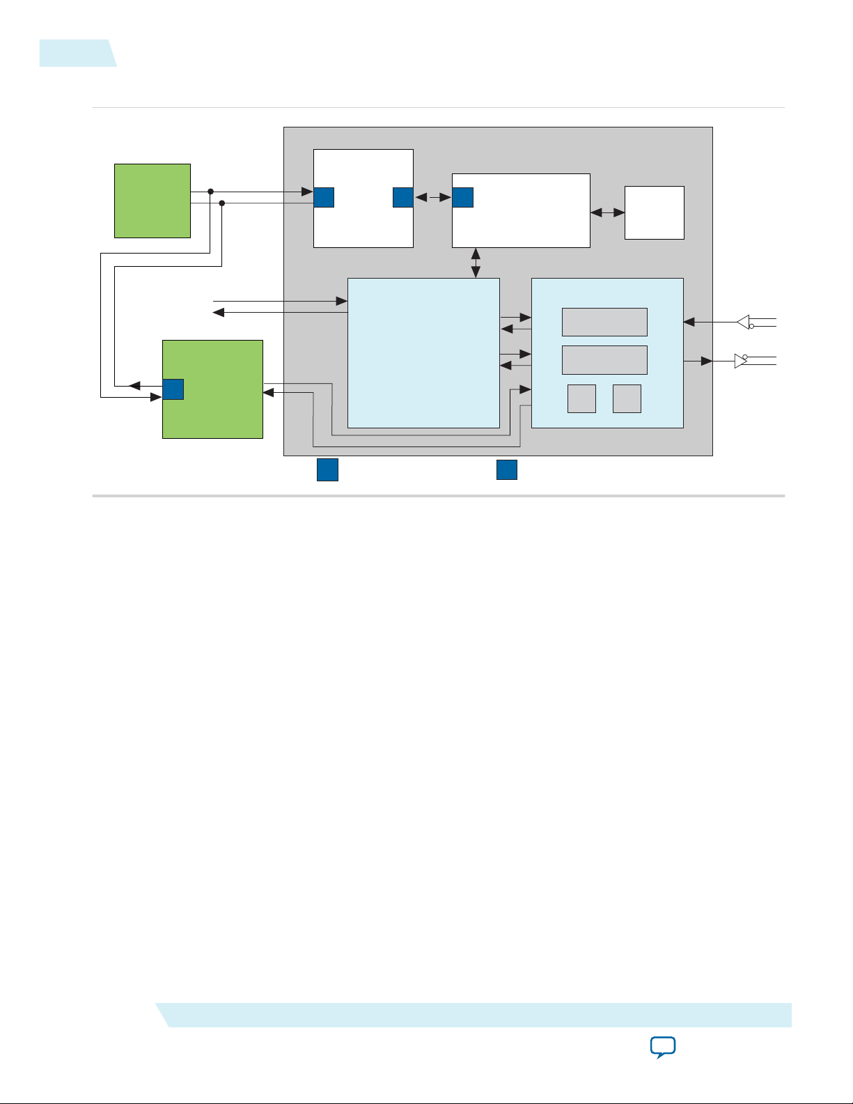
To MAC
To HSSI Pins
Transceiver PHY
PMA PCS
Customized functionality for:
10GBASE-R
10GBASE-KR
1G/10GBASE-R
XAUI
Interlaken
PCI Express PIPE
Avalon-ST
TX and RX
Avalon-MM
Control &
Status
PCS & PMA
Control & Status
Register Memory Map
S
Reset
Controller
S
Altera Transceiver
Reconfiguration
Controller
Offset Cancellation
Analog Settings
Avalon-MM PHY
Management
Read & Write
Control & Status
Registers
M
Avalon-MM master interface
M
S
Avalon-MM slave interface
S
PLL CDR
Rx Deserializer
Tx Serializer
Embedded
Controller
1-2
Native Transceiver PHYs
Figure 1-1: Transceiver PHY Top-Level Modules
UG-01080
2015.01.19
Native Transceiver PHYs
Altera Corporation
Related Information
• 10GBASE-R PHY IP Core on page 3-1
• Backplane Ethernet 10GBASE-KR PHY IP Core Overview
• 1G/10 Gbps Ethernet PHY IP Core on page 5-1
• XAUI PHY IP Core on page 6-1
• Interlaken PHY IP Core on page 7-1
• PHY IP Core for PCI Express (PIPE) on page 8-1
Each device family, beginning with Series V devices offers a separate Native PHY IP core to provide lowlevel access to the hardware. There are separate IP Cores for Arria V, Arria V GZ, Cyclone V, and Stratix
V devices.
The Native PHYs allow you to customize the transceiver settings to meet your requirements. You can also
use the Native PHYs to dynamically reconfigure the PCS datapath. Depending on protocol mode selected,
built-in rules validate the options you specify. The following figure illustrates the Stratix V Native PHY.
Introduction to the Protocol-Specific and Native Transceiver PHYs
Send Feedback
Page 14
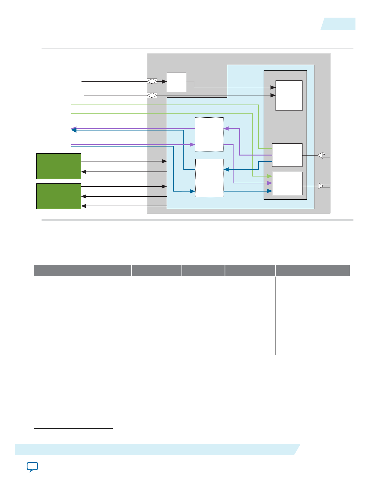
PLLs
PMA
altera _xcvr_native_ <dev>
Transceiver Native PHY
Transceiver
Reconfiguration
Controller
Reconfiguration to XCVR
Reconfiguration from XCVR
TX and RX Resets
Calilbration Busy
PLL and RX Locked
RX PCS Parallel Data
TX PCS Parallel Data
CDR Reference Clock
(when neither PCS is enabled)
TX PLL Reference Clock
Serializer/
Clock
Generation
Block
RX Serial Data
to
FPGA fabric
Transceiver
PHY Reset
Controller
TX PMA Parallel Data
RX PMA Parallel Data
TX Serial Data
Serializer
Deserializer
Standard
PCS
(optional)
10G PCS
(optional)
UG-01080
2015.01.19
Figure 1-2: Stratix V Transceiver Native PHY IP Core
Native Transceiver PHYs
1-3
As shown, the Stratix V Native PHY connects to the separately instantiated Transceiver Reconfiguration
Controller and Transceiver PHY Reset Controller.
Table 1-1: Native Transceiver PHY Datapaths
Datapaths Stratix V Arria V Arria V GZ Cyclone V
PMA Direct:
Yes Yes Yes -
This datapath connects the
FPGA fabric directly to the
PMA, minimizing latency.
You must implement any
required PCS functions in the
FPGA fabric.
(1)
Introduction to the Protocol-Specific and Native Transceiver PHYs
(1)
PMA Direct mode is supported for Arria V GT, ST, and GZ devices, and for Stratix V GT devices only.
Send Feedback
Altera Corporation
Page 15

1-4
Non-Protocol-Specific Transceiver PHYs
Datapaths Stratix V Arria V Arria V GZ Cyclone V
UG-01080
2015.01.19
Standard:
Yes Yes Yes Yes
This datapath provides a
complete PCS and PMA for
the TX and RX channels. You
can customize the Standard
datapath by enabling or
disabling individual modules
and specifying data widths.
10G:
Yes - Yes -
This is a high performance
datapath. It provides a
complete PCS and PMA for
the TX and RX channels. You
can customize the 10G
datapath by enabling or
disabling individual modules
and specifying data widths.
Related Information
• Analog Settings for Arria V Devices on page 19-2
• Analog Settings for Arria V GZ Devices on page 19-11
• Analog Settings for Cyclone V Devices on page 19-26
• Analog Settings for Stratix V Devices on page 19-34
Non-Protocol-Specific Transceiver PHYs
Non-protocol specific transceiver PHYs provide more flexible settings than the protocol-specific
transceiver PHYs. They include the Custom PHY, Low Latency PHY, and Deterministic Latency PHY IP
Cores.
These PHYs include an Avalon® Memory-Mapped (Avalon-MM) interface to access control and status
registers and an Avalon Streaming (Avalon-ST) interface to connect to the MAC for data transfer.
Related Information
• Custom PHY IP Core on page 9-1
• Deterministic Latency PHY IP Core on page 11-1
• Low Latency PHY IP Core on page 10-1
Transceiver PHY Modules
The following sections provide a brief introduction to the modules included in the transceiver PHYs.
Altera Corporation
Introduction to the Protocol-Specific and Native Transceiver PHYs
Send Feedback
Page 16

UG-01080
2015.01.19
Transceiver Reconfiguration Controller
PCS
The PCS implements part of the physical layer specification for networking protocols. Depending upon
the protocol that you choose, the PCS may include many different functions. Some of the most commonly
included functions are: 8B/10B, 64B/66B, or 64B/67B encoding and decoding, rate matching and clock
compensation, scrambling and descrambling, word alignment, phase compensation, error monitoring,
and gearbox.
PMA
The PMA receives and transmits differential serial data on the device external pins. The transmit (TX)
channel supports programmable pre-emphasis and programmable output differential voltage (VOD). It
converts parallel input data streams to serial data. The receive (RX) channel supports offset cancellation to
correct for process variation and programmable equalization. It converts serial data to parallel data for
processing in the PCS. The PMA also includes a clock data recovery (CDR) module with separate CDR
logic for each RX channel.
Avalon-MM PHY Management Interface
You can use the Avalon-MM PHY Management module to read and write the control and status registers
in the PCS and PMA for the protocol-specific transceiver PHY. The Avalon-MM PHY Management
module includes both Avalon-MM master and slave ports and acts as a bridge. It transfers commands
received from an embedded controller on its slave port to its master port. The Avalon-MM PHY
management master interface connects the Avalon-MM slave ports of PCS and PMA registers and the
Transceiver Reconfiguration module, allowing you to manage these Avalon-MM slave components
through a simple, standard interface. (Refer to Transceiver PHY Top-Level Modules.)
1-5
Transceiver Reconfiguration Controller
Altera Transceiver Reconfiguration Controller dynamically reconfigures analog settings in Arria V,
Cyclone V, and Stratix V devices.
Reconfiguration allows you to compensate for variations due to process, voltage, and temperature (PVT)
in 28-nm devices. It is required for Arria V, Cyclone V, and Stratix V devices that include transceivers.
For more information about the Transceiver Reconfiguration Controller, refer to Transceiver Reconfigu‐
ration Controller IP Core. The reset controller may be included in the transceiver PHY or may be a
separately instantiated component as described in Transceiver PHY Reset Controller.
Related Information
Transceiver Reconfiguration Controller IP Core Overview on page 16-1
Resetting the Transceiver PHY
This section provides an overview of the embedded reset controller and the separately instantiated
Transceiver PHY Reset Controller IP Core.
The embedded reset controller ensures reliable transceiver link initialization. The reset controller initial‐
izes both the TX and RX channels. You can disable the automatic reset controller in the Custom, Low
Latency Transceiver, and Deterministic Latency PHYs. If you disable the embedded reset controller, the
powerdown, analog and digital reset signals for both the TX and RX channels are top-level ports of the
transceiver PHY. You can use these ports to design a custom reset sequence, or you can use the Alteraprovided Transceiver Reset Controller IP Core.
Introduction to the Protocol-Specific and Native Transceiver PHYs
Send Feedback
Altera Corporation
Page 17

1-6
Running a Simulation Testbench
UG-01080
2015.01.19
The Transceiver PHY Reset Controller IP Core handles all reset sequencing of the transceiver to enable
successful operation. Because the Transceiver PHY Reset Controller IP is available in clear text, you can
also modify it to meet your requirements. For more information about the Transceiver PHY Reset
Controller, refer to Transceiver Reconfiguration Controller IP Core.
To accommodate different reset requirements for different transceivers in your design, instantiate
multiple instances of a PHY IP core. For example, if your design includes 20 channels of the Custom PHY
IP core with 12 channels running a custom protocol using the automatic reset controller and 8 channels
requiring manual control of RX reset, instantiate 2 instances of the Custom PHY IP core and customize
one to use automatic mode and the other to use your own reset logic. For more information, refer to
“Enable embedded reset control” in Custom PHY General Options.
For more information about reset control in Stratix V devices, refer to Transceiver Reset Control in Stratix
V Devices in volume 3 of the Stratix V Device Handbook. For Stratix IV devices, refer to Reset Control and
Power Down in volume 4 of the Stratix IV Device Handbook. For Arria V devices, refer to Transceiver
Reset Control and Power-Down in Arria V Devices. For Cyclone V devices refer to Transceiver Reset
Control and Power Down in Cyclone V Devices.
Related Information
• General Options Parameters on page 9-3
• Transceiver PHY Reset Controller IP Core on page 17-1
• Transceiver Reset Control in Stratix V Devices
• Reset Control and Power Down
• Transceiver Reset Control and Power-Down in Arria V Devices
• Transceiver Reset Control and Power Down in Cyclone V Devices
Running a Simulation Testbench
When you generate your transceiver PHY IP core, the Quartus® II software generates the HDL files that
define your parameterized IP core. In addition, the Quartus II software generates an example Tcl script to
compile and simulate your design in ModelSim.
Altera Corporation
Introduction to the Protocol-Specific and Native Transceiver PHYs
Send Feedback
Page 18
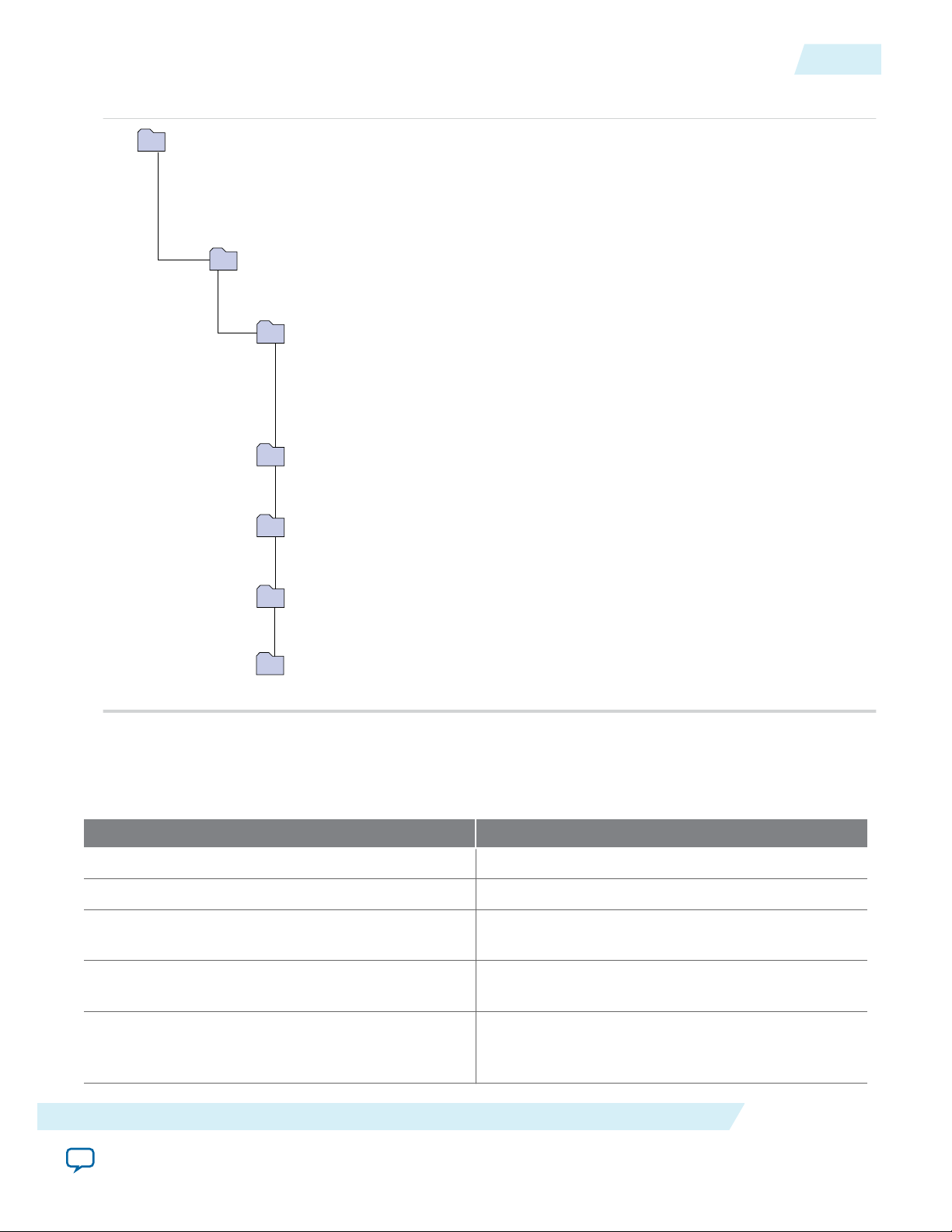
<instance_name> _sim/synopsys Simulation files for Synopsys simulation tools
<project_dir>
<project_dir>/<instance_name> - includes PHY IP Verilog HDL and
SystemVerilog design files for synthesis
<instance_name>. v or .vhd - the parameterized transceiver PHY IP core
<instance_name> .qip - lists all files used in the transceiver PHY IP design
<instance_name> .bsf - a block symbol file for you transceiver PHY IP core
<instance_name> _sim/altera_xcvr <PHY_IP_name> - includes plain text
files that describe all necessary files required for a successful simulation. The
plain text files contain the names of all required files and the correct order
for reading these files into your simulation tool.
<instance_name> _sim/aldec Simulation files for Riviera-PRO simulation tools
<instance_name> _sim/cadence Simulation files for Cadence simulation tools
<instance_name> _sim/mentor Simulation files for Mentor simulation tools
UG-01080
2015.01.19
Figure 1-3: Directory Structure for Generated Files
Running a Simulation Testbench
1-7
Table 1-2: Transceiver PHY Files and Directories
The following table describes the key files and directories for the parameterized transceiver PHY IP core
and the simulation environment which are in clear text.
<project_dir> The top-level project directory.
<instance_name> .v or .vhd The top-level design file.
<instance_name> .qip A list of all files necessary for Quartus II compila‐
<instance_name> .bsf A Block Symbol File (.bsf) for your transceiver
File Name Description
tion.
PHY.
<project_dir>/<instance_name>/ The directory that stores the HDL files that define
the protocol-specific PHY IP core. These files are
used for synthesis.
Introduction to the Protocol-Specific and Native Transceiver PHYs
Send Feedback
Altera Corporation
Page 19

1-8
Running a Simulation Testbench
File Name Description
sv_xcvr_native.sv Defines the transceiver. It includes instantiations of
the PCS and PMA modules and Avalon-MM PHY
management interface.
stratixv_hssi_ <module_name> _rbc. sv These files perform rule based checking for the
module specified. For example, if the PLL type, data
rate, and FPGA fabric transceiver interface width
are not compatible, the checker reports an error.
altera_wait_generate.v Generates waitrequest for protocol-specific
transceiver PHY IP core that includes backpressure.
alt_reset_ctrl_tgx_cdrauto.sv Includes the reset controller logic.
<instance_name> _phy_assignments.qip Includes an example of the PLL_TYPE assignment
statement required to specify the PLL type for each
PLL in the design. The available types are clock
multiplier unit (CMU) and auxiliary transmit
(ATX).
UG-01080
2015.01.19
<project_dir>/<instance_name> _sim/ altera_xcvr_
The simulation directory.
<PHY_IP_name>/
<project_dir>/<instance_name>_sim/ aldec Simulation files for Riviera-PRO simulation tools.
<project_dir>/<instance_name>_sim/ cadence Simulation files for Cadence simulation tools.
<project_dir>/<instance_name>_sim/ mentor Simulation files for Mentor simulation tools.
<project_dir>/<instance_name>_sim/ synopsys Simulation files for Synopsys simulation tools.
The Verilog and VHDL transceiver PHY IP cores have been tested with the following simulators:
• ModelSim SE
• Synopsys VCS MX
• Cadence NCSim
If you select VHDL for your transceiver PHY, only the wrapper generated by the Quartus II software is in
VHDL. All the underlying files are written in Verilog or System Verilog. To enable simulation using a
VHDL-only ModelSim license, the underlying Verilog and System Verilog files for the transceiver PHY
are encrypted so that they can be used with the top-level VHDL wrapper without using a mixed-language
simulator.
For more information about simulating with ModelSim, refer to the Mentor Graphics ModelSim Support
chapter in volume 3 of the Quartus II Handbook.
The transceiver PHY IP cores do not support the NativeLink feature in the Quartus II software.
Generating Custom Simulation Scripts for Multiple Transceiver PHYs with ip-make-simscript
Use the ip-make-simscript utility to generate simulation command scripts for multiple transceiver
PHYs or Qsys systems. Specify all Simulation Package Descriptor files (.spd). The .spd files list the
required simulation files for the corresponding IP core. The MegaWizard Plug-In Manager and Qsys
generate the .spd files.
Altera Corporation
Introduction to the Protocol-Specific and Native Transceiver PHYs
Send Feedback
Page 20

UG-01080
2015.01.19
When you specify multiple .spd files, the ip-make-simscript utility generates a single simulation script
containing all required simulation information. The default value of TOP_LEVEL_NAME is the
TOP_LEVEL_NAME defined in the IP core or Qsys .spd file. If this is not the top-level instance in your
design, specify the top-level instance of your testbench or design.
You can set appropriate variables in the script or edit the variable assignments directly in the script. If the
simulation script is a Tcl file that can be sourced in the simulator, set the variables before sourcing the
script. If the simulation script is a shell script, pass in the variables as command-line arguments to shell
script.
To run ip-make-simscript , type the following at the command prompt:
<ACDS installation path>\quartus\sopc_builder\bin\ip-make-simscript
The following tables lists some of the options available with this utility.
Table 1-3: Options for the ip-make-simscript Utility
Option Description Status
Unsupported Features
1-9
--spd=<file>
Describes the list of compiled files and
memory model hierarchy. If your design
Require
d
includes multiple IP cores or Qsys systems
that include .spd files, use this option for each
file. For example:
ip-make-simscript --spd=ip1.spd -spd=ip2.spd
--outputdirectory=<directory>
Directory path specifying the location of
output files. If unspecified, the default setting
Option
al
is the directory from which ip-make-
simscript is run.
--compile-to-work
Compiles all design files to the default work
library. Use this option only if you encounter
Option
al
problems managing your simulation with
multiple libraries.
--use-relative-paths Uses relative paths whenever possible Option
al
To learn about all options for the ip-make-simscript , type the following at the command prompt:
<ACDS installation path>\quartus\sopc_builder\bin\ip-make-simscript --help
Related Information
• Mentor Graphics ModelSim Support
• Simulating Altera Designs
Unsupported Features
The protocol-specific and native transceiver PHYs are not supported in Qsys in the current release.
Introduction to the Protocol-Specific and Native Transceiver PHYs
Send Feedback
Altera Corporation
Page 21

2015.01.19
<path>
Installation directory
ip
Contains the Altera IP Library and third-party IP cores
altera
Contains the Altera IP Library
alt_mem_if
Contains the UniPHY IP core files
www.altera.com
101 Innovation Drive, San Jose, CA 95134
Getting Started Overview
2
UG-01080
Subscribe
Send Feedback
This chapter provides a general overview of the Altera IP core design flow to help you quickly get started
with any Altera IP core.
The Altera IP Library is installed as part of the Quartus II installation process. You can select and
parameterize any Altera IP core from the library. Altera provides an integrated parameter editor that
allows you to customize IP cores to support a wide variety of applications. The parameter editor guides
you through the setting of parameter values and selection of optional ports. The following sections
describe the general design flow and use of Altera IP cores.
Installation and Licensing of IP Cores
The Altera IP Library is distributed with the Quartus II software and downloadable from the Altera
website.
The following figure shows the directory structure after you install an Altera IP core, where <path> is the
installation directory. The default installation directory on Windows is C:\altera\<version number>; on
Linux it is /opt/altera<version number>.
Figure 2-1: IP Core Directory Structure
You can evaluate an IP core in simulation and in hardware until you are satisfied with its functionality
and performance. Some IP cores require that you purchase a license for the IP core when you want to take
your design to production. After you purchase a license for an Altera IP core, you can request a license file
from the Altera Licensing page of the Altera website and install the license on your computer. For
additional information, refer to Altera Software Installation and Licensing.
©
2015 Altera Corporation. All rights reserved. ALTERA, ARRIA, CYCLONE, ENPIRION, MAX, MEGACORE, NIOS, QUARTUS and STRATIX words and logos are
trademarks of Altera Corporation and registered in the U.S. Patent and Trademark Office and in other countries. All other words and logos identified as
trademarks or service marks are the property of their respective holders as described at www.altera.com/common/legal.html. Altera warrants performance
of its semiconductor products to current specifications in accordance with Altera's standard warranty, but reserves the right to make changes to any
products and services at any time without notice. Altera assumes no responsibility or liability arising out of the application or use of any information,
product, or service described herein except as expressly agreed to in writing by Altera. Altera customers are advised to obtain the latest version of device
specifications before relying on any published information and before placing orders for products or services.
ISO
9001:2008
Registered
Page 22
Select Design Flow
Specify Parameters
Qsys or
SOPC Builder
Flow
MegaWizard
Flow
Complete Qsys or
SOPC Builder System
Specify Parameters
IP Complete
Perform
Functional Simulation
Debug Design
Does
Simulation Give
Expected Results?
Yes
Optional
Add Constraints
and Compile Design
2-2
Design Flows
Related Information
• Altera
• Altera Licensing
• Altera Software Installation and Licensing
Design Flows
This section describes how to parameterize Altera IP cores.
You can use the following flow(s) to parameterize Altera IP cores:
Figure 2-2: Design Flows
(2)
UG-01080
2015.01.19
The MegaWizard Plug-In Manager flow offers the following advantages:
• Allows you to parameterize an IP core variant and instantiate into an existing design
• For some IP cores, this flow generates a complete example design and testbench
(2)
Altera IP cores may or may not support the Qsys and SOPC Builder design flows.
Altera Corporation
Getting Started Overview
Send Feedback
Page 23

UG-01080
2015.01.19
MegaWizard Plug-In Manager Flow
This section describes how to specify parameters and simulate your IP core with the MegaWizard Plug-In
Manager.
The MegaWizard™ Plug-In Manager flow allows you to customize your IP core and manually integrate
the function into your design.
Specifying Parameters
To specify IP core parameters, follow these steps:
1. Create a Quartus II project using the New Project Wizard available from the File menu.
2. In the Quartus II software, launch the IP Catalog.
3. You can select the IP core for your protocol implementation from the IP Catalog.
4. Specify the parameters on the Parameter Settings pages. For detailed explanations of these
parameters, refer to the "Parameter Settings" chapter in this document or the "Documentation" button
in the MegaWizard parameter editor.
Note: Some IP cores provide preset parameters for specific applications. If you wish to use preset
parameters, click the arrow to expand the Presets list, select the desired preset, and then click
Apply. To modify preset settings, in a text editor modify the <installation directory>/ip/altera/
alt_mem_if_interfaces/alt_mem_if_<memory_protocol>_emif/
alt_mem_if_<memory_protocol>_mem_model.qprs file.
5. If the IP core provides a simulation model, specify appropriate options in the wizard to generate a
simulation model.
MegaWizard Plug-In Manager Flow
2-3
Note:
Altera IP supports a variety of simulation models, including simulation-specific IP functional
simulation models and encrypted RTL models, and plain text RTL models. These are all
cycle-accurate models. The models allow for fast functional simulation of your IP core instance
using industry-standard VHDL or Verilog HDL simulators. For some cores, only the plain text
RTL model is generated, and you can simulate that model.
Note: For more information about functional simulation models for Altera IP cores, refer to
Simulating Altera Designs in volume 3 of the Quartus II Handbook.
Caution: Use the simulation models only for simulation and not for synthesis or any other purposes.
Using these models for synthesis creates a nonfunctional design.
6. If the parameter editor includes EDA and Summary tabs, follow these steps:
a. Some third-party synthesis tools can use a netlist that contains the structure of an IP core but no
detailed logic to optimize timing and performance of the design containing it. To use this feature if
your synthesis tool and IP core support it, turn on Generate netlist.
b. On the Summary tab, if available, select the files you want to generate. A gray checkmark indicates
a file that is automatically generated. All other files are optional.
Note:
If file selection is supported for your IP core, after you generate the core, a generation report
(<variation name>.html)appears in your project directory. This file contains information
about the generated files.
7. Click the Finish button, the parameter editor generates the top-level HDL code for your IP core, and a
simulation directory which includes files for simulation.
Getting Started Overview
Send Feedback
Altera Corporation
Page 24

2-4
Simulate the IP Core
Note: The Finish button may be unavailable until all parameterization errors listed in the messages
window are corrected.
8. Click Yes if you are prompted to add the Quartus II IP File (.qip) to the current Quartus II project.
You can also turn on Automatically add Quartus II IP Files to all projects.
You can now integrate your custom IP core instance in your design, simulate, and compile. While
integrating your IP core instance into your design, you must make appropriate pin assignments. You can
create a virtual pin to avoid making specific pin assignments for top-level signals while you are simulating
and not ready to map the design to hardware.
For some IP cores, the generation process also creates complete example designs. An example design for
hardware testing is located in the < variation_name > _example_design/example_project/ directory. An
example design for RTL simulation is located in the < variation_name > _example_design/simulation/
directory.
Note:
For information about the Quartus II software, including virtual pins, refer to Quartus II Help.
Related Information
• Simulating Altera Designs
• Quartus II Help
Simulate the IP Core
This section describes how to simulate your IP core.
UG-01080
2015.01.19
You can simulate your IP core variation with the functional simulation model and the testbench or
example design generated with your IP core. The functional simulation model and testbench files are
generated in a project subdirectory. This directory may also include scripts to compile and run the
testbench.
For a complete list of models or libraries required to simulate your IP core, refer to the scripts provided
with the testbench.
For more information about simulating Altera IP cores, refer to Simulating Altera Designs in volume 3 of
the Quartus II Handbook.
Related Information
Simulating Altera Designs
Altera Corporation
Getting Started Overview
Send Feedback
Page 25

2015.01.19
10GBASE-R PHY IP Core
10.3125 Gbps serial
XFI/SFP+
Stratix V FPGA
PMA
Hard PCS
10GBASE-R
64b/66b
Scrambler
Gearbox
SDR XGMII
72 bits @ 156.25 Mbps
Avalon-MM
Control & Status
Transceiver
Reconfiguraiton
www.altera.com
101 Innovation Drive, San Jose, CA 95134
10GBASE-R PHY IP Core
3
UG-01080
Subscribe
Send Feedback
The Altera 10GBASE-R PHY IP Core implements the functionality described in IEEE Standard 802.3
Clause 45.
It delivers serialized data to an optical module that drives optical fiber at a line rate of 10.3125 gigabits per
second (Gbps). In a multi-channel implementation of 10GBASE-R, each channel of the 10GBASE-R PHY
IP Core operates independently. Both the PCS and PMA of the 10GBASE-R PHY are implemented as
hard IP blocks in Stratix V devices, saving FPGA resources.
Figure 3-1: 10GBASE-R PHY with Hard PCS with PMA in Stratix V Devices
Note: For a 10-Gbps Ethernet solution that includes both the Ethernet MAC and the 10GBASE-R PHY,
Note: For more detailed information about the 10GBASE-R transceiver channel datapath, clocking, and
The following figure illustrates a multiple 10 GbE channel IP core in a Stratix IV GT device. To achieve
higher bandwidths, you can instantiate multiple channels. The PCS is available in soft logic for Stratix IV
GT devices; it connects to a separately instantiated hard PMA. The PCS connects to an Ethernet MAC via
single data rate (SDR) XGMII running at 156.25 megabits per second (Mbps) and transmits data to a 10
Gbps transceiver PMA running at 10.3125 Gbps in a Stratix IV GT device.
©
2015 Altera Corporation. All rights reserved. ALTERA, ARRIA, CYCLONE, ENPIRION, MAX, MEGACORE, NIOS, QUARTUS and STRATIX words and logos are
trademarks of Altera Corporation and registered in the U.S. Patent and Trademark Office and in other countries. All other words and logos identified as
trademarks or service marks are the property of their respective holders as described at www.altera.com/common/legal.html. Altera warrants performance
of its semiconductor products to current specifications in accordance with Altera's standard warranty, but reserves the right to make changes to any
products and services at any time without notice. Altera assumes no responsibility or liability arising out of the application or use of any information,
product, or service described herein except as expressly agreed to in writing by Altera. Altera customers are advised to obtain the latest version of device
specifications before relying on any published information and before placing orders for products or services.
refer to the 10-Gbps Ethernet MAC MegaCore Function User Guide.
channel placement, refer to the “10GBASE-R” section in the Transceiver Configurations in Stratix V
Devices chapter of the Stratix V Device Handbook.
ISO
9001:2008
Registered
Page 26
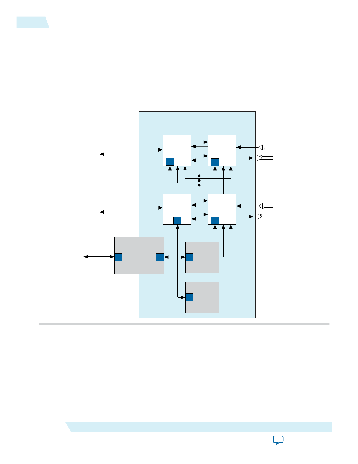
To MAC
To Embedded
Controller
Avalon-MM
connections
10GBASE-R PHY - Stratix IV Device
SDR XGMII
72 bits @ 156.25 Mbps
To MAC
SDR XGMII
72 bits @ 156.25 Mbps
Avalon-MM
PHY
Management
Bridge
M
S
S
Low Latency
Controller
S
Transceiver
Reconfig
Controller
Alt_PMA
10GBASE-R
10.3 Gbps
10.3125 Gbps serial
To HSSI Pins
PCS
10GBASE-R
(64b/66b)
S
S
Alt_PMA
10GBASE-R
10.3 Gbps
10.3125 Gbps serial
To HSSI Pins
PCS
10GBASE-R
(64b/66b)
S
S
3-2
10GBASE-R PHY IP Core
To make the most effective use of this soft PCS and PMA configuration for Stratix IV GT devices, you can
group up to four channels in a single quad and control their functionality using one Avalon-MM PHY
management bridge, transceiver reconfiguration module, and low controller. As this figure illustrates, the
Avalon-MM bridge Avalon-MM master port connects to the Avalon-MM slave port of the transceiver
reconfiguration and low latency controller modules so that you can update analog settings using the
standard Avalon-MM interface.
Note: This configuration does not require that all four channels in a quad run the 10GBASE-R protocol.
Figure 3-2: Complete 10GBASE-R PHY Design in Stratix IV GT Device
UG-01080
2015.01.19
Altera Corporation
The following figures illustrate the 10GBASE-R in Arria V GT, Arria V GZ, and Stratix V GX devices.
10GBASE-R PHY IP Core
Send Feedback
Page 27
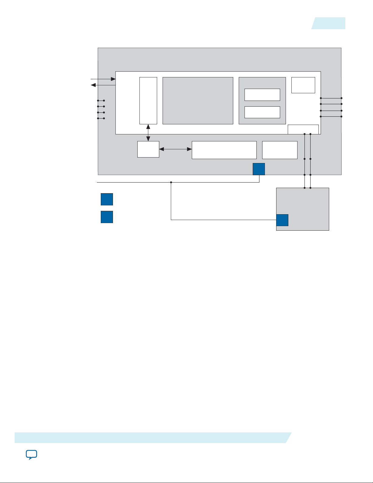
Transceiver
Reconfiguration
Controller
Data
Wiring
Soft PCS
TX PMA
PMA
RX PMA & CDR
CMU
PLL
Reset
Controller
Avalon-MM Slave
Avalon-MM Master
PMA + Reset Control & Status
(Memory Map)
10-GB BaseR
CSR
Tx Serial
Rx Serial
Reconfiguration
Avalon-MM
Management
Interface
to Embedded
Controller
Control & Status
Conduits
(Optional or by
I/F Specification)
Avalon-ST
Streaming
Data
Tx Data
Rx Data
Arria V GT 10GBASE-R Top Level
Arria V GT 10GBASE-R
To/From
Transceiver
S
M
S
S
UG-01080
2015.01.19
Figure 3-3: 10GBASE-R PHY IP Core In Arria V GT Devices
10GBASE-R PHY IP Core
3-3
10GBASE-R PHY IP Core
Send Feedback
Altera Corporation
Page 28
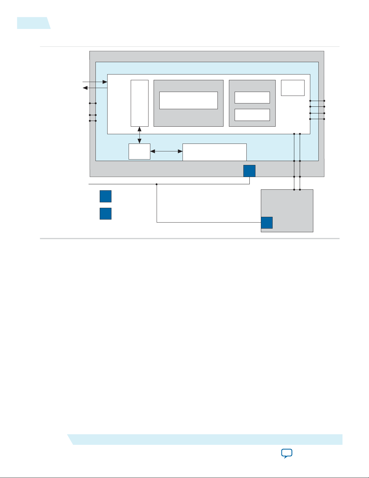
Data
Wiring
PLD-PCS & Duplex PCS
PCS-PMA
PCS
TX PMA
PMA
RX PMA & CDR
Generic
PLL
Reset
Controller
Transceiver
Reconfiguration
Controller
S
PMA + Reset Control & Status
(Memory Map)
Tx Serial
Rx Serial
S
Control & Status
(Optional or by
I/F Specification)
Avalon-ST
Streaming
Data
Tx Data
Rx Data
Transceiver Protocol
Arria V GZ Transceiver Protocol
To/From
XCVR
Avalon-MM Slave
Avalon-MM Master
S
M
Avalon-MM
Management
Interface
to Embedded
Controller
3-4
10GBASE-R PHY IP Core
Figure 3-4: 10GBASE-R PHY IP Core In Arria V GZ Devices
UG-01080
2015.01.19
Altera Corporation
10GBASE-R PHY IP Core
Send Feedback
Page 29
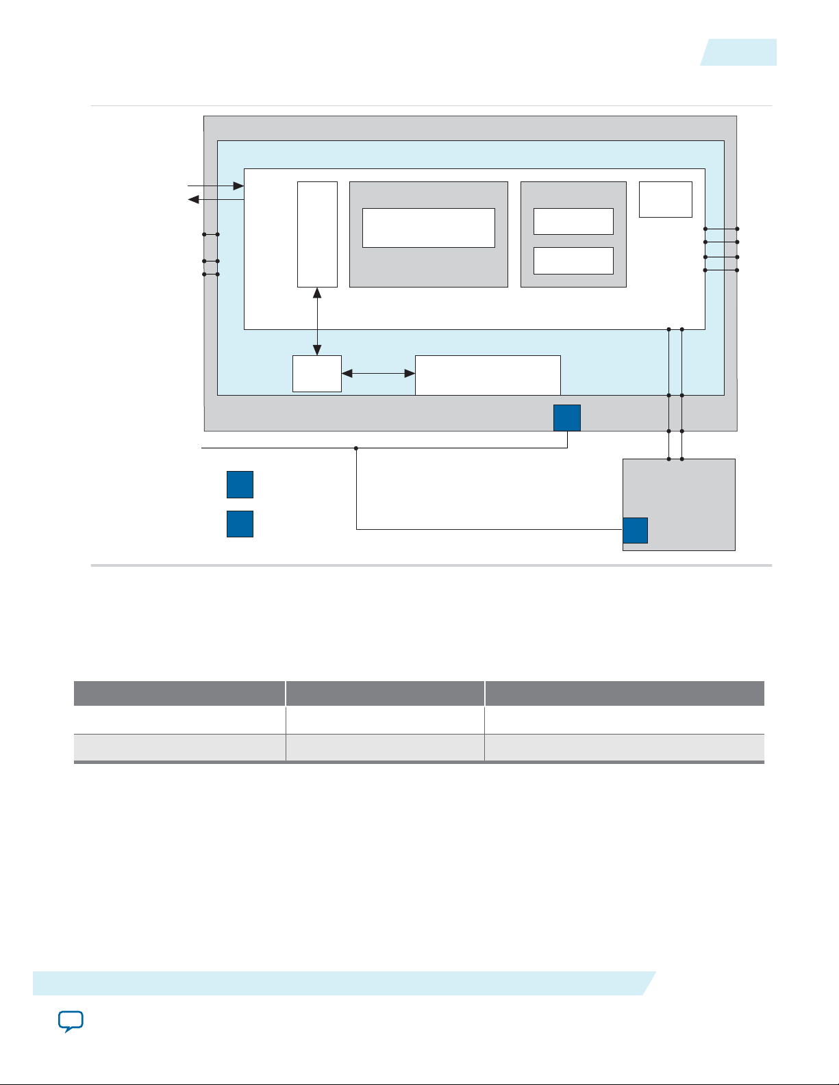
Data
Wiring
PLD-PCS & Duplex PCS
PCS-PMA
PCS
TX PMA
PMA
RX PMA & CDR
Generic
PLL
Reset
Controller
PMA + Reset Control & Status
(Memory Map)
Tx Serial
Rx Serial
S
Control & Status
(Optional or by
I/F Specification)
Avalon-ST
Streaming
Data
Tx Data
Rx Data
Transceiver Protocol
Stratix V Transceiver Protocol
To/From
XCVR
Avalon-MM Slave
Avalon-MM Master
S
M
Avalon-MM
Management
Interface
to Embedded
Controller
Transceiver
Reconfiguration
Controller
S
UG-01080
2015.01.19
Figure 3-5: 10GBASE-R PHY IP Core In Stratix V Devices
10GBASE-R PHY IP Core
3-5
10GBASE-R PHY IP Core
The following table lists the latency through the PCS and PMA for Arria V GT devices with a 66-bit PMA.
The FPGA fabric to PCS interface is 64 bits wide. The frequency of the parallel clock is 156.25 MHz which
is line rate (10.3125 Gpbs)/interface width (64).
Table 3-1: Latency for TX and RX PCS and PMA Arria V Devices
TX 28 131
RX 33 99
The following table lists the latency through the PCS and PMA for Stratix V devices with a 40-bit PMA.
The FPGA fabric to PCS interface is 64 bits wide. The frequency of the parallel clock is 156.25 MHz which
PCS (Parallel Clock Cycles PMA (UI)
is line rate (10.3125 Gbps)/interface width (64).
Send Feedback
Altera Corporation
Page 30

3-6
10GBASE-R PHY Release Information
Table 3-2: Latency for TX and RX PCS and PMA Stratix V Devices
PCS (Parallel Clock Cycles)
Minimum Maximum Minimum Maximum
TX 7 12 8 12 124
RX 14 33 15 34 43
Related Information
• IEEE 802.3 Clause 49
• 10-Gbps Ethernet MAC MegaCore Function User Guide
• Transceiver Configurations in Stratix V Devices
10GBASE-R PHY Release Information
Release information for the IP core.
UG-01080
2015.01.19
PMA (UI)32-bit PMA Width 40-bit PMA Width
Table 3-3: 10GBASE-R Release Information
Item Description
Version 13.1
Release Date November 2013
Ordering Codes
(3)
IP-10GBASERPCS (primary) IPR-10GBASERPCS
(renewal)
Product ID 00D7
Vendor ID 6AF7
10GBASE-R PHY Device Family Support
Device support for the IP core.
IP cores provide either final or preliminary support for target Altera device families. These terms have the
following definitions:
• Final support—Verified with final timing models for this device.
• Preliminary support—Verified with preliminary timing models for this device.
Table 3-4: Device Family Support
Arria V GT devices–Soft PCS and Hard PMA Final
(3)
No ordering codes or license files are required for Stratix V devices.
Altera Corporation
Device Family Support
10GBASE-R PHY IP Core
Send Feedback
Page 31

UG-01080
2015.01.19
Device Family Support
Arria V ST devices-Soft PCS and Hard PMA Final
Arria V GZ Final
Stratix IV GT devices–Soft PCS and Hard PMA Final
Stratix V devices–Hard PCS and PMA Final
Other device families No support
Note: For speed grade information, refer to “Transceiver Performance Specifications” in the DC and
Switching Characteristics chapter in the Stratix IV Handbook for Stratix IV devices or Stratix V
Device Datasheet.
Related Information
• DC and Switching Characteristics
• Stratix V Device Datasheet.
10GBASE-R PHY Performance and Resource Utilization for Stratix IV Devices
10GBASE-R PHY Performance and Resource Utilization for Stratix IV
3-7
Devices
Because the 10GBASE-R PHY is implemented in hard logic it uses less than 1% of the available ALMs,
memory, primary and secondary logic registers. The following table lists the typical expected device
resource utilization for duplex channels using the current version of the Quartus II software targeting a
Stratix IV GT device. The numbers of combinational ALUTs, logic registers, and memory bits are
rounded to the nearest 100.
Table 3-5: 10GBASE-R PHY Performance and Resource Utilization—Stratix IV GT Device
Channels Combinational ALUTs Logic Registers (Bits) Memory Bits
1 5200 4100 4700
4 15600 1300 18800
10 38100 32100 47500
10GBASE-R PHY Performance and Resource Utilization for Arria V GT Devices
The following table lists the resource utilization when targeting an Arria V (5AGTFD7K3F4015) device.
Resource utilization numbers reflect changes to the resource utilization reporting starting in the Quartus
II software v12.1 release for 28 nm device families and upcoming device families. The numbers of ALMs
and logic registers are rounded up to the nearest 100.
Note:
10GBASE-R PHY IP Core
Send Feedback
For information about Quartus II resource utilization reporting, refer to Fitter Resources Reports
in the Quartus II Help.
Altera Corporation
Page 32

3-8
10GBASE-R PHY Performance and Resource Utilization for Arria V GZ and Stratix V Devices
Table 3-6: 10GBASE-R PHY Performance and Resource Utilization—Arria V GT Device
UG-01080
2015.01.19
Channels ALMs Primary Logic
Registers
Secondary Logic
Registers
Memory 10K
1 2800 3000 300 7
Related Information
Fitter Resources Reports
10GBASE-R PHY Performance and Resource Utilization for Arria V GZ and
Stratix V Devices
Because the 10GBASE-R PHY is implemented in hard logic in Arria V GZ and Stratix V devices, it uses
less than 1% of the available ALMs, memory, primary and secondary logic registers.
The following table lists the total latency for an Ethernet packet with a 9600 byte payload and an interpacket gap of 12 characters. The latency includes the number of cycles to transmit the payload from the
TX XGMII interface, through the TX PCS and PMA, looping back through the RX PMA and PCS to the
RX XGMII interface. (Stratix V Clock Generation and Distribution illustrates this datapath.)
Table 3-7: Latency
PPM Difference Cycles
0 PPM 35
-200 PPM 35
+200 PPM 42
Note: If latency is critical, Altera recommends designing your own soft 10GBASE-R PCS and connecting
to the Low Latency PHY IP Core.
Parameterizing the 10GBASE-R PHY
The 10GBASE-R PHY IP Core is available for the Arria V, Arria V GZ, Stratix IV, or Stratix V device
families. Complete the following steps to configure the 10GBASE-R PHY IP Core:
1. Under Tools > IP Catalog, select the device family of your choice.
2. Under Tools > IP Catalog > Interface Protocols > Ethernet > select 10GBASE-R PHY.
3. Use the tabs on the MegaWizard Plug-In Manager to select the options required for the protocol.
4. Refer to the following topics to learn more about the parameters:
a. General Option Parameters on page 3-9
b. Analog Parameters for Stratix IV Devices on page 3-12
5. Click Finish to generate your parameterized 10GBASE-R PHY IP Core.
Altera Corporation
10GBASE-R PHY IP Core
Send Feedback
Page 33

UG-01080
2015.01.19
General Option Parameters
This section describes general parameters.
This section describes the 10GBASE-R PHY parameters, which you can set using the MegaWizard Plug-
In Manager.
Table 3-8: General Options
Name Value Description
General Options
General Option Parameters
3-9
Device family
Arria V
Specifies the target device.
Arria V GZ
Stratix IV GT
Stratix V
Number of channels 1-32 The total number of 10GBASE-R PHY channels.
Mode of operation
Duplex
Arria V and Stratix V devices allow duplex, TX, or
RX mode. Stratix IV GT devices only support duplex
TX Only
mode.
RX Only
PLL type CMU, ATX
For Arria V GZ, Stratix IV, and Stratix V devices:
You can select either the CMU or ATX PLL. The
CMU PLL has a larger frequency range than the
ATX PLL. The ATX PLL is designed to improve
jitter performance and achieves lower channel-tochannel skew. Another advantage of the ATX PLL is
that it does not use a transceiver channel, while the
CMU PLL does.
Reference Clock Frequency
10GBASE-R PHY IP Core
Send Feedback
322.265625
MHz
644.53125 MHz
Altera recommends the ATX PLL for data rates <= 8
Gbps.
Arria V and Stratix V devices support both frequen‐
cies. Stratix IV GT devices only support 644.53125
MHz.
Altera Corporation
Page 34

3-10
General Option Parameters
Name Value Description
UG-01080
2015.01.19
PCS / PMA interface width
32
40
For Stratix V and Arria V GZ devices only:
Specifies the data interface width between the 10G
PCS and the transceiver PMA. Smaller width
corresponds to lower PCS latency but higher
frequency.
• For 40 bit width, rx_recovered_clock is 257.8125
MHz and the gearbox ratio is 66:40.
• For 40 bit width, rx_recovered_clock is
322.265626 MHz and the gearbox ratio is 66:32.
32 bit PCS / PMA interface with does not support
data rates up to 10.3125 Gbps in C4/I4 Arria V GZ
device variants. Refer to Arria V GZ Device
Datasheet for details on data rates supported by
different device variants.
Additional Options
Enable additional control and
status pins
On/Off If you turn this option On, the following 2 signals
are brought out to the top level of the IP core to
facilitate debugging: rx_hi_ber and rx_block_lock.
Enable rx_recovered_clk pin On/Off When you turn this option On, the RX recovered
clock signal is an output signal.
Enable pll_locked status port On/Off
For Arria V and Stratix V devices:
When you turn this option On, a PLL locked status
signal is included as a top-level signal of the core.
Use external PMA control and
On/Off
For Stratix IV devices:
reconfig
If you turn this option on, the PMA controller and
reconfiguration block are external, rather than
included in the 10GBASE-R PHY IP Core, allowing
you to use the same PMA controller and reconfigu‐
ration IP cores for other protocols in the same
transceiver quad.
When you turn this option On, the cal_blk_
powerdown (0x021) and pma_tx_pll_is_locked
(0x022) registers are available.
Enable rx_coreclkin port On/Off When selected, rx_coreclkin is sourced from the
156.25 MHz xgmii_rx_clk signal avoiding the use
of a FPLL to generate this clock. This clock drives
the read side of RX FIFO.
Altera Corporation
10GBASE-R PHY IP Core
Send Feedback
Page 35

UG-01080
2015.01.19
General Option Parameters
Name Value Description
Enable embedded reset control On/Off When On, the automatic reset controller initiates
the reset sequence for the transceiver. When Off you
can design your own reset logic using tx_analogr-
eset , rx_analogreset, tx_digitalreset, rx_
digitalreset, and pll_powerdown which are
top-level ports of the Custom Transceiver PHY. You
may also use the Transceiver PHY Reset Controller
to reset the transceivers. For more information, refer
to the Transceiver Reconfiguration Controller IP
Core . By default, the CDR circuitry is in automatic
lock mode whether you use the embedded reset
controller or design your own reset logic. You can
switch the CDR to manual mode by writing the pma_
rx_setlocktodata or pma_rx_set_locktoref
registers to 1. If either the pma_rx_set_locktodata
and pma_rx_set_locktoref is set, the CDR
automatic lock mode is disabled.
3-11
Starting channel number 0-96
For Stratix IV devices, specifies the starting channel
number. Must be 0 or a multiple of 4. You only need
to set this parameter if you are using external PMA
and reconfiguration modules.
In Stratix V devices, by default, the logical channel 0
is assigned to either physical transceiver channel 1 or
channel 4 of a transceiver bank. However, if you
have already created a PCB with a different lane
assignment for logical channel 0, you can use the
work around shown in the example below.
Assignment of the starting channel number is
required for serial transceiver dynamic reconfigura‐
tion.
Enable IEEE 1588 latency
adjustment ports
On/Off When you turn this option On, the core includes
logic to implement the IEEE 1588 Precision Time
Protocol.
Example 3-1: Changing the Default Logical Channel 0 Channel Assignments in Stratix V Devices
for ×6 or ×N Bonding
This example shows how to change the default logical channel 0 assignment in Stratix V devices
by redefining the pma_bonding_master parameter using the Quartus II Assignment Editor. In
this example, the pma_bonding_master was originally assigned to physical channel 1. (The
original assignment could also have been to physical channel 4.) The to parameter reassigns the
10GBASE-R PHY IP Core
Send Feedback
Altera Corporation
Page 36

3-12
Analog Parameters for Stratix IV Devices
pma_bonding_master to the 10GBASE-R instance name. You must substitute the instance name
from your design for the instance name shown in quotation marks.
set_parameter -name pma_bonding_master "\"1\"" -to "<PHY IP instance name>"
Related Information
• Transceiver PHY Reset Controller IP Core on page 17-1
• 1588 Delay Requirements on page 3-30
• Arria V GZ Device Datasheet
Analog Parameters for Stratix IV Devices
For Stratix IV devices, you specify analog options on the Analog Options tab.
Table 3-9: PMA Analog Options for Stratix IV Devices
Name Value Description
UG-01080
2015.01.19
Transmitter termination
resistance
Transmitter VOD control
setting
Pre-emphasis pre-tap
setting
Invert the pre-emphasis
pre-tap polarity setting
Pre-emphasis first posttap setting
Pre-emphasis second
post-tap setting
Invert the pre-emphasis
second post-tap polarity
OCT_85_OHMS,
Indicates the value of the termination resistor for
the transmitter.
OCT_100_OHMS,
OCT_120_OHMS,
OCT_150_OHMS
0–7 Sets VOD for the various TX buffers.
0–7 Sets the amount of pre-emphasis on the TX buffer.
On, Off
Determines whether or not the pre-emphasis
control signal for the pre-tap is inverted. If you
turn this option on, the pre-emphasis control
signal is inverted.
0-15 Sets the amount of pre-emphasis for the 1st post-
tap.
0–7 Sets the amount of pre-emphasis for the 2nd post-
tap.
On, Off Determines whether or not the pre-emphasis
control signal for the second post-tap is inverted.
If you turn this option on, the pre-emphasis
control signa is inverted.
Altera Corporation
10GBASE-R PHY IP Core
Send Feedback
Page 37

UG-01080
2015.01.19
10GBASE-R PHY Interfaces
Name Value Description
3-13
Receiver common mode
Tri-State
Specifies the RX common mode voltage.
voltage
0.82V
1.1v
Receiver termination
resistance
OCT_85_OHMS
Indicates the value of the termination resistor for
the receiver.
OCT_100_OHMs
OCT_120_OHMS
OCT_150_OHMS
Receiver DC 0-4 Sets the equalization DC gain using one of the
following settings:
• 0: 0 dB
• 1: 3 dB
• 2: 6 dB
• 3: 9 dB
• 4: 12 dB
Receiver static equalizer
setting:
0-15 This option sets the equalizer control settings. The
equalizer uses a pass band filter. Specifying a low
value passes low frequencies. Specifying a high
value passes high frequencies.
Analog Parameters for Arria V, Arria V GZ, and Stratix V Devices
Click on the appropriate links to review the analog parameters for these devices.
Related Information
• Analog Settings for Arria V Devices on page 19-2
• Analog Settings for Arria V GZ Devices on page 19-11
• Analog Settings for Stratix V Devices on page 19-34
10GBASE-R PHY Interfaces
This section describes the 10GBASE-R PHY interfaces.
The following figure illustrates the top-level signals of the 10BASE-R PHY; <n> is the channel number.
10GBASE-R PHY IP Core
Send Feedback
Altera Corporation
Page 38

xgmii_tx_dc<n>[71:0]
tx_ready
xgmii_tx_clk
xgmii_rx_dc<n>[71:0]
rx_ready
rx_data_ready[<n>-1:0]
xgmii_rx_clk
rx_coreclkin
phy_mgmt_clk
phy_mgmt_clk_reset
phy_mgmt_addr[8:0]
phy_mgmt_writedata[31:0]
phy_mgmt_readdata[31:0]
phy_mgmt_write
phy_mgmt_read
phy_mgmt_waitrequest
10GBASE-R Top-Level Signals
Dynamic
Reconfiguration
External
PMA Control
Stratix IV
Devices
rx_serial_data<n>
tx_serial_data<n>
gxb_pdn
pll_pdn
cal_blk_pdn
cal_blk_clk
pll_locked
reconfig_to_xcvr[3:0]
reconfig_from_xcvr[<n>/4)17-1:0]
reconfig_to_xcvr[(<n>70-1):0]
reconfig_from_xcvr[(<n>46-1):0]
rx_block_lock
rx_hi_ber
rx_recovered_clk[<n>]
rx_latency_adj<n>[15:0]
tx_latency_adj<n>[15:0]
pll_ref_clk
Transceiver
Serial Data
SDR XGMII TX
Inputs from MAC
SDR XGMII RX
Outputs from PCS
towards MAC
Avalon-MM PHY
Management
Interface
Status, 1588
and Reference`
Clock
pll_powerdown
tx_digitalreset [<n>-1:0]
tx_analogreset [<n>-1:0]
tx_cal_busy [<n>-1:0]
rx_digitalreset [<n>-1:0]
rx_analogreset [<n>-1:0]
rx_cal_busy [<n>-1:0]
Reset Control
and Status
(Optional)
3-14
10GBASE-R PHY Data Interfaces
Figure 3-6: 10GBASE-R PHY Top-Level Signals
UG-01080
2015.01.19
Note: The block diagram shown in the GUI labels the external pins with the interface type and places the
interface name inside the box. The interface type and name are used in the Hardware Component
Description File (_hw.tcl). If you turn on Show signals, the block diagram displays all top-level
signal names.
For more information about _hw.tcl files refer to refer to the Component Interface Tcl Reference chapter
in volume 1 of the Quartus II Handbook.
Related Information
Component Interface Tcl Reference
10GBASE-R PHY Data Interfaces
This section describes the 10GBASE-R PHY data interfaces.
The TX signals are driven from the MAC to the PCS. The RX signals are driven from the PCS to the
MAC.
Table 3-10: SDR XGMII TX Inputs
Signal Name Direction Description
XGMII TX Interface
Altera Corporation
10GBASE-R PHY IP Core
Send Feedback
Page 39

UG-01080
2015.01.19
10GBASE-R PHY Data Interfaces
Signal Name Direction Description
xgmii_tx_dc_[<n>71:0] Input Contains 8 lanes of data and control for
XGMII. Each lane consists of 8 bits of data and
1 bit of control.
• Lane 0-[7:0]/[8]
• Lane 1-[16:9]/[17]
• Lane 2-[25:18]/[26]
• Lane 3-[34:27]/[35]
• Lane 4-[43:36]/[44]
• Lane 5-[52:45]/[53]
• Lane 6-[61:54]/[62]
• Lane 7-[70:63]/[71]
Refer toTable 3-11 for the mapping of the
xgmii_tx_dc data and control to the xgmii_
sdr_data and xgmii_sdr_ctrl signals.
tx_ready Output Asserted when the TX channel is ready to
transmit data. Because the readyLatency on
this Avalon-ST interface is 0, the MAC may
drive tx_ready as soon as it comes out of reset.
3-15
xgmii_tx_clk Input The XGMII TX clock which runs at 156.25
MHz. Connect xgmii_tx_clk to xgmii_rx_
clk to guarantee this clock is within 150 ppm
of the transceiver reference clock.
XGMII RX Interface
xgmii_rx_dc_<n>[71:0] Output Contains 8 lanes of data and control for
XGMII. Each lane consists of 8 bits of data and
1 bit of control.
• Lane 0-[7:0]/[8]
• Lane 1-[16:9]/[17]
• Lane 2-[25:18]/[26]
• Lane 3-[34:27]/[35]
• Lane 4-[43:36]/[44]
• Lane 5-[52:45]/[53]
• Lane 6-[61:54]/[62]
• Lane 7-[70:63]/[71]
Refer toTable 3-12 for the mapping of the
xgmii_rx_dc data and control to the xgmii_
sdr_data and xgmii_sdr_ctrl signals.
rx_ready Output Asserted when the RX reset is complete.
10GBASE-R PHY IP Core
Send Feedback
Altera Corporation
Page 40

3-16
10GBASE-R PHY Data Interfaces
Signal Name Direction Description
rx_data_ready [<n>-1:0] Output When asserted, indicates that the PCS is
sending data to the MAC. Because the
readyLatency on this Avalon-ST interface is 0,
the MAC must be ready to receive data
whenever this signal is asserted. After rx_
ready is asserted indicating the exit from the
reset state, the MAC should store xgmii_rx_
dc_<n>[71:0] in each cycle where rx_data_
ready<n> is asserted.
xgmii_rx_clk Output This clock is generated by the same reference
clock that is used to generate the transceiver
clock. Its frequency is 156.25 MHz. Use this
clock for the MAC interface to minimize the
size of the FIFO between the MAC and SDR
XGMII RX interface.
rx_coreclkin Input When you turn on Create rx_coreclkin port,
this signal is available as a 156.25 MHz clock
input port to drive the RX datapath interface
(RX read FIFO).
UG-01080
2015.01.19
Serial Interface
rx_serial_data_<n> Input Differential high speed serial input data using
the PCML I/O standard. The clock is recovered
from the serial data stream.
tx_serial_data_<n> Output Differential high speed serial input data using
the PCML I/O standard. The clock is
embedded from the serial data stream.
Table 3-11: Mapping from XGMII TX Bus to XGMII SDR Bus
Signal Name XGMII Signal Name Description
xgmii_tx_dc_[7:0] xgmii_sdr_data[7:0] Lane 0 data
xgmii_tx_dc_[8] xgmii_sdr_ctrl[0] Lane 0 control
xgmii_tx_dc_[16:9] xgmii_sdr_data[15:8] Lane 1 data
xgmii_tx_dc_[17] xgmii_sdr_ctrl[1] Lane 1 control
xgmii_tx_dc_[25:18] xgmii_sdr_data[23:16] Lane 2 data
xgmii_tx_dc_[26] xgmii_sdr_ctrl[2] Lane 2 control
xgmii_tx_dc_[34:27] xgmii_sdr_data[31:24] Lane 3 data
xgmii_tx_dc_[35] xgmii_sdr_ctrl[3] Lane 3 control
xgmii_tx_dc_[43:36] xgmii_sdr_data[39:32] Lane 4 data
Altera Corporation
10GBASE-R PHY IP Core
Send Feedback
Page 41

UG-01080
2015.01.19
10GBASE-R PHY Status, 1588, and PLL Reference Clock Interfaces
Signal Name XGMII Signal Name Description
xgmii_tx_dc_[44] xgmii_sdr_ctrl[4] Lane 4 control
xgmii_tx_dc_[52:45] xgmii_sdr_data[47:40] Lane 5 data
xgmii_tx_dc_[53] xgmii_sdr_ctrl[5] Lane 5 control
xgmii_tx_dc_[61:54] xgmii_sdr_data[55:48] Lane 6 data
xgmii_tx_dc_[62] xgmii_sdr_ctrl[6] Lane 6 control
xgmii_tx_dc_[70:63] xgmii_sdr_data[63:56] Lane 7 data
xgmii_tx_dc_[71] xgmii_sdr_ctrl[7] Lane 7 control
Table 3-12: Mapping from XGMII RX Bus to the XGMII SDR Bus
Signal Name XGMII Signal Name Description
xgmii_rx_dc_[7:0] xgmii_sdr_data[7:0] Lane 0 data
xgmii_rx_dc_[8] xgmii_sdr_ctrl[0] Lane 0 control
xgmii_rx_dc_[16:9] xgmii_sdr_data[15:8] Lane 1 data
3-17
xgmii_rx_dc_[17] xgmii_sdr_ctrl[1] Lane 1 control
xgmii_rx_dc_[25:18] xgmii_sdr_data[23:16] Lane 2 data
xgmii_rx_dc_[26] xgmii_sdr_ctrl[2] Lane 2 control
xgmii_rx_dc_[34:27] xgmii_sdr_data[31:24] Lane 3 data
xgmii_rx_dc_[35] xgmii_sdr_ctrl[3] Lane 3 control
xgmii_rx_dc_[43:36] xgmii_sdr_data[39:32] Lane 4 data
xgmii_rx_dc_[44] xgmii_sdr_ctrl[4] Lane 4 control
xgmii_rx_dc_[52:45] xgmii_sdr_data[47:40] Lane 5 data
xgmii_rx_dc_[53] xgmii_sdr_ctrl[5] Lane 5 control
xgmii_rx_dc_[61:54] xgmii_sdr_data[55:48] Lane 6 data
xgmii_rx_dc_[62] xgmii_sdr_ctrl[6] Lane 6 control
xgmii_rx_dc_[70:63] xgmii_sdr_data[63:56] Lane 7 data
xgmii_rx_dc_[71] xgmii_sdr_ctrl[7] Lane 7 control
10GBASE-R PHY Status, 1588, and PLL Reference Clock Interfaces
This section describes the 10GBASE-R PHY status, 1588, and PLL reference clock interfaces.
10GBASE-R PHY IP Core
Send Feedback
Altera Corporation
Page 42

3-18
Optional Reset Control and Status Interface
Table 3-13: 10GBASE-R Status, 1588, and PLL Reference Clock Outputs
Signal Name Direction Description
rx_block_lock Output Asserted to indicate that the block synchron‐
izer has established synchronization.
rx_hi_ber Output Asserted by the BER monitor block to
indicate a Sync Header high bit error rate
greater than 10-4.
rx_recovered_clk[<n>:0] Output This is the RX clock, which is recovered from
the received data stream.
pll_locked Output When asserted, indicates that the TX PLL is
locked.
IEEE 1588 Precision Time Protocol
rx_latency_adj_10g [15:0] Output When you enable 1588, this signal outputs
the real time latency in XGMII clock cycles
(156.25 MHz) for the RX PCS and PMA
datapath for 10G mode. Bits 0 to 9 represent
the fractional number of clock cycles. Bits 10
to 15 represent the number of clock cycles.
UG-01080
2015.01.19
tx_latency_adj_10g [15:0] Output When you enable 1588, this signal outputs
real time latency in XGMII clock cycles
(156.25 MHz) for the TX PCS and PMA
datapath for 10G mode. Bits 0 to 9 represent
the fractional number of clock cycles. Bits 10
to 15 represent the number of clock cycles.
PLL Reference Clock
pll_ref_clk Input For Stratix IV GT devices, the TX PLL
reference clock must be 644.53125 MHz. For
Arria V and Stratix V devices, the TX PLL
reference clock can be either 644.53125 MHz
or 322.265625 MHz.
Optional Reset Control and Status Interface
This topic describes the signals in the optional reset control and status interface. These signals are
available if you do not enable the embedded reset controller.
Table 3-14: Avalon-ST RX Interface
Signal Name Direction Description
pll_powerdown Input When asserted, resets the TX PLL.
Altera Corporation
10GBASE-R PHY IP Core
Send Feedback
Page 43

UG-01080
2015.01.19
10GBASE-R PHY Clocks for Arria V GT Devices
Signal Name Direction Description
tx_digitalreset[<n>-1:0] Input When asserted, reset all blocks in the TX PCS. If
your design includes bonded TX PCS channels,
refer to Timing Constraints for Reset Signals when
Using Bonded PCS Channels for a SDC constraint
you must include in your design.
tx_analogreset[<n>-1:0] Input When asserted, resets all blocks in the TX PMA.
Note: For Arria V devices, while compiling a
multi-channel transceiver design, you
will see a compile warning (12020) in
Quartus II software related to the signal
width of tx_analogreset. You can safely
ignore this warning. Also, per-channel
TX analog reset is not supported in
Quartus II software. Channel 0 TX
analog resets all the transceiver
channels.
tx_cal_busy[<n>-1:0] Output When asserted, indicates that the initial TX
calibration is in progress. It is also asserted if
reconfiguration controller is reset. It will not be
asserted if you manually re-trigger the calibration
IP. You must hold the channel in reset until
calibration completes.
3-19
rx_digitalreset[<n>-1:0] Input When asserted, resets the RX PCS.
rx_analogreset[<n>-1:0] Input When asserted, resets the RX CDR.
rx_cal_busy[<n>-1:0] Output When asserted, indicates that the initial RX
calibration is in progress. It is also asserted if
reconfiguration controller is reset. It will not be
asserted if you manually re-trigger the calibration
IP.
Related Information
• Timing Constraints for Bonded PCS and PMA Channels on page 17-10
• Transceiver Reset Control in Stratix V Devices
• Transceiver Reset Control in Arria V Devices
• Transceiver Reset Control in Cyclone V Devices
10GBASE-R PHY Clocks for Arria V GT Devices
The following figure illustrates Arria V GT clock generation and distribution.
10GBASE-R PHY IP Core
Send Feedback
Altera Corporation
Page 44

10GBASE-R Transceiver Channel - Arria V GT
TX PCS
(soft)
RX PCS
(soft)
TX PMA
(hard)
RX PMA
(hard)
TX PLL
64
64
64
64
80
80
xgmii_tx_clk
156.25 MHz
161.1328 MHz
161.1328 MHz
10.3125 Gbps
10.3125 Gbps
pll_ref_clk
644.53125 MHz
8/33
fPLL
rx_coreclkin
RX
TX
3-20
10GBASE-R PHY Clocks for Arria V GZ Devices
Figure 3-7: Arria V GT Clock Generation and Distribution
UG-01080
2015.01.19
10GBASE-R PHY Clocks for Arria V GZ Devices
The following figure illustrates clock generation and distribution for Arria V GZ devices.
Altera Corporation
10GBASE-R PHY IP Core
Send Feedback
Page 45

pll_ref_clk
644.53125 MHz
10.3125
Gbps serial
257.8125
MHz
257.8125
MHz
156.25 MHz
10GBASE-R Hard IP Transceiver Channel - Arria V GZ
TX
RX
TX PCS
40
TX PMA
10.3125
Gbps serial
RX PCS
40
RX PMA
TX PLL
8/33
fPLL
xgmii_rx_clk
rx_coreclkin
xgmii_tx_clk
64-bit data, 8-bit control
64-bit data, 8-bit control
UG-01080
2015.01.19
Figure 3-8: Arria V GZ Clock Generation and Distribution
10GBASE-R PHY Clocks for Stratix IV Devices
3-21
10GBASE-R PHY Clocks for Stratix IV Devices
The phy_mgmt_clk_reset signal is the global reset that resets the entire PHY. A positive edge on this
signal triggers a reset.
Refer to the Reset Control and Power Down chapter in volume 2 of the Stratix IV Device Handbook for
additional information about reset sequences in Stratix IV devices.
The PCS runs at 257.8125 MHz using the pma_rx_clock provided by the PMA. You must provide the
PMA an input reference clock running at 644.53725 MHz to generate the 257.8125 MHz clock.
10GBASE-R PHY IP Core
Send Feedback
Altera Corporation
Page 46

pll_ref_clk
644.53125 MHz
10.3125
Gbps serial
516.625
MHz
257.8125
MHz
516.625
MHz
257.8125
MHz
156.25 MHz
10GBASE-R Transceiver Channel - Stratix IV GT
TX
RX
TX PCS
(hard IP)
TX PCS
(soft IP)
2040
64-bit data, 8-bit control
64-bit data, 8-bit control
TX PMA
/2
10.3125
Gbps serial
RX PCS
(hard IP)
RX PCS
(soft IP)
2040
RX PMA
/2
5/4
TX PLL
8/33
GPLL
xgmii_rx_clk
xgmii_tx_clk
3-22
10GBASE-R PHY Clocks for Stratix V Devices
Figure 3-9: Stratix IV Clock Generation and Distribution
UG-01080
2015.01.19
Related Information
Reset Control and Power Down
10GBASE-R PHY Clocks for Stratix V Devices
Altera Corporation
The following figure illustrates clock generation and distribution in Stratix V devices.
10GBASE-R PHY IP Core
Send Feedback
Page 47

pll_ref_clk
644.53125 MHz
10.3125
Gbps serial
257.8125
MHz
257.8125
MHz
156.25 MHz
10GBASE-R Hard IP Transceiver Channel - Stratix V
TX
RX
TX PCS
40
TX PMA
10.3125
Gbps serial
RX PCS
40
RX PMA
TX PLL
8/33
fPLL
xgmii_rx_clk
rx_coreclkin
xgmii_tx_clk
64-bit data, 8-bit control
64-bit data, 8-bit control
UG-01080
2015.01.19
10GBASE-R PHY Register Interface and Register Descriptions
Figure 3-10: Stratix V Clock Generation and Distribution
3-23
To ensure proper functioning of the PCS, the maximum PPM difference between the pll_ref_clk and
xgmii_tx_clk clock inputs is 0 PPM. The FIFO in the RX PCS can compensate ±100 PPM between the
RX PMA clock and xgmii_rx_clk. You should use xgmii_rx_clk to drive xgmii_tx_clk. The CDR logic
recovers 257.8125 MHz clock from the incoming data.
10GBASE-R PHY Register Interface and Register Descriptions
The Avalon-MM PHY management interface provides access to the 10GBASER-R PHY PCS and PMA
registers. You can use an embedded controller acting as an Avalon-MM master to send read and write
commands to this Avalon-MM slave interface.
10GBASE-R PHY IP Core
Altera Corporation
Send Feedback
Page 48

3-24
10GBASE-R PHY Register Interface and Register Descriptions
Table 3-15: Avalon-MM PHY Management Interface
Signal Name Direction Description
phy_mgmt_clk Input The clock signal that controls the Avalon-MM
PHY management, interface. For Stratix IV
devices, the frequency range is 37.5-50 MHz.
There is no frequency restriction for Stratix V
devices; however, if you plan to use the same clock
for the PHY management interface and
transceiver reconfiguration, you must restrict the
frequency range of phy_mgmt_clk to 100-150
MHz to meet the specification for the transceiver
reconfiguration clock.
phy_mgmt_clk_reset Input Global reset signal that resets the entire 10GBASE-
R PHY. This signal is active high and level
sensitive. This signal is not synchronized
internally.
phy_mgmt_addr[8:0] Input 9-bit Avalon-MM address.
UG-01080
2015.01.19
phy_mgmt_writedata[31:0] Input Input data.
phy_mgmt_readdata[31:0] Output Output data.
phy_mgmt_write Input Write signal. Asserted high.
phy_mgmt_read Input Read signal. Asserted high.
phy_mgmt_waitrequest Output When asserted, indicates that the Avalon-MM
slave interface is unable to respond to a read or
write request. When asserted, control signals to
the Avalon-MM slave interface must remain
constant.
Refer to the “Typical Slave Read and Write Transfers” and “Master Transfers” sections in the “Avalon
Memory-Mapped Interfaces” chapter of the Avalon Interface Specifications for timing diagrams.
The following table specifies the registers that you can access over the Avalon-MM PHY management
interface using word addresses and a 32-bit embedded processor. A single address space provides access
to all registers.
Writing to reserved or undefined register addresses may have undefined side effects.
Note:
Table 3-16: 10GBASE-R Register Descriptions
Word Addr Bit R/W Name Description
Altera Corporation
PMA Common Control and Status
10GBASE-R PHY IP Core
Send Feedback
Page 49

UG-01080
2015.01.19
10GBASE-R PHY Register Interface and Register Descriptions
Word Addr Bit R/W Name Description
0x021 [31:0] RW cal_blk_powerdown Writing a 1 to channel <n> powers
down the calibration block for
channel <n>. This register is only
available if you select Use external
PMA control and reconfig on the
Additional Options tab of the GUI.
0x022 [31:0] RO pma_tx_pll_is_locked Bit[P] indicates that the TX clock
multiplier unit CMU PLL [P] is
locked to the input reference clock.
This register is only available if you
select Use external PMA control and
reconfig on the Additional Options
tab of the GUI.
Reset Control Registers-Automatic Reset Controller
0x041 [31:0] RW reset_ch_bitmask Reset controller channel bitmask for
digital resets. The default value is all 1
s. Channel <n> can be reset when
bit<n> = 1. Channel <n> cannot be
reset when bit<n>=0.
3-25
0x042 [1:0]
WO reset_control (write) Writing a 1 to bit 0 initiates a TX
digital reset using the reset controller
module. The reset affects channels
enabled in the reset_ch_bitmask.
Writing a 1 to bit 1 initiates a RX
digital reset of channels enabled in the
reset_ch_bitmask. Both bits 0 and 1
self-clear.
RO reset_status (read) Reading bit 0 returns the status of the
reset controller TX ready bit. Reading
bit 1 returns the status of the reset
controller RX ready bit.
10GBASE-R PHY IP Core
Send Feedback
Altera Corporation
Page 50

3-26
10GBASE-R PHY Register Interface and Register Descriptions
Word Addr Bit R/W Name Description
[31:0] RW reset_fine_control You can use the reset_fine_
control register to create your own
reset sequence. The reset control
module performs a standard reset
sequence at power on and whenever
the phy_mgmt_clk_reset is asserted.
Bits [31:4,0] are reserved.
[31:4,0] RW Reserved It is safe to write 0s to reserved bits.
[1] RW reset_tx_digital Writing a 1 causes the internal TX
digital reset signal to be asserted,
resetting all channels enabled in
0x044
reset_ch_bitmask. You must write a
0 to clear the reset condition.
[2] RW reset_rx_analog Writing a 1 causes the internal RX
digital reset signal to be asserted,
resetting the RX analog logic of all
channels enabled in reset_ch_
bitmask. You must write a 0 to clear
the reset condition.
UG-01080
2015.01.19
[3] RW reset_rx_digital Writing a 1 causes the RX digital reset
signal to be asserted, resetting the RX
digital channels enabled in reset_ch_
bitmask. You must write a 0 to clear
the reset condition.
PMA Channel Control and Status
RW phy_serial_loopback Writing a 1 to channel <n> puts
channel <n> in serial loopback mode.
0x061 [31:0]
For information about pre- or post-
CDR serial loopback modes, refer to
Loopback Modes.
0x064 [31:0] RW pma_rx_set_locktodata When set, programs the RX CDR PLL
to lock to the incoming data. Bit <n>
corresponds to channel <n>.
0x065 [31:0] RW pma_rx_set_locktoref When set, programs the RX CDR PLL
to lock to the reference clock. Bit <n>
corresponds to channel <n>.
0x066 [31:0] RO pma_rx_is_lockedtodata When asserted, indicates that the RX
CDR PLL is locked to the RX data,
and that the RX CDR has changed
from LTR to LTD mode. Bit <n>
corresponds to channel <n>.
Altera Corporation
10GBASE-R PHY IP Core
Send Feedback
Page 51

UG-01080
2015.01.19
10GBASE-R PHY Register Interface and Register Descriptions
Word Addr Bit R/W Name Description
0x067 [31:0] RO pma_rx_is_lockedtoref When asserted, indicates that the RX
CDR PLL is locked to the reference
clock. Bit <n> corresponds to channel
<n>.
10GBASE-R PCS
Provides for indirect addressing of all
PCS control and status registers. Use
0x080 [31:0] WO INDIRECT_ADDR
this register to specify the logical
channel number of the PCS channel
you want to access.
[2] RW RCLR_ERRBLK_CNT When set to 1, clears the error block
count register. To block: Block
synchronizer
0x081
[3] RW RCLR_BER_COUNT When set to 1, clears the bit error rate
(BER) register. To block: BER
monitor
3-27
0x082
[0] R PCS_STATUS For Stratix IV devices: When asserted
indicates that the PCS link is up.
[1] R HI_BER When asserted by the BER monitor
block, indicates that the PCS is
recording a high BER. From block:
BER monitor
[2] R BLOCK_LOCK When asserted by the block
synchronizer, indicates that the PCS
is locked to received blocks. From
Block: Block synchronizer
[3] R TX_FIFO_FULL When asserted, indicates the TX FIFO
is full. From block: TX FIFO
[4] R RX_FIFO_FULL When asserted, indicates the RX FIFO
is full. From block: RX FIFO
[5] R RX_SYNC_HEAD_ERROR For Stratix V devices, when asserted,
indicates an RX synchronization
error. This signal is Stratix V devices
only.
[6] R RX_SCRAMBLER_ERROR For Stratix V devices: When asserted,
indicates an RX scrambler error.
10GBASE-R PHY IP Core
Send Feedback
[7] R RX_DATA_READY When asserted indicates that the RX
interface is ready to send out received
data. From block: 10 Gbps Receiver
PCS
Altera Corporation
Page 52

3-28
10GBASE-R PHY Dynamic Reconfiguration for Stratix IV Devices
Word Addr Bit R/W Name Description
[5:0] R BER_COUNT[5:0] For Stratix IV devices only, records
the bit error rate (BER). From block:
BER monitor
[13:6] R ERROR_BLOCK_COUNT[7:0] For Stratix IV devices only, records
the number of blocks that contain
0x083
errors. From Block: Block synchron‐
izer
[14] R LATCHED_HI_BER Latched version of HI_BER . From
block: BER monitor
[15] R LATCHED_BLOCK_LOCK Latched version of BLOCK_LOCK. From
Block: Block synchronizer
Related Information
• Loopback Modes on page 16-58
• Avalon Interface Specifications
UG-01080
2015.01.19
10GBASE-R PHY Dynamic Reconfiguration for Stratix IV Devices
The 10GBASE-R PHY includes additional top-level signals when configured with an external modules for
PMA control and dynamic reconfiguration.
You enable this configuration by turning on Use external PMA control and reconfig available for Stratix
IV GT devices.
Table 3-17: External PMA and Reconfiguration Signals
Signal Name Direction Description
gxb_pdn Input When asserted, powers down the entire GT block.
Active high. For Stratix IV de
pll_pdn Input When asserted, powers down the TX PLL. Active high.
cal_blk_pdn Input When asserted, powers down the calibration block.
Active high.
cal_blk_clk Input Calibration clock. For Stratix IV devices only. It must
be in the range 37.5-50 MHz. You can use the same
clock for the phy_mgmt_clk and the cal_blk_clk.
pll_locked Output When asserted, indicates that the TX PLL is locked.
reconfig_to_xcvr[3:0] Input Reconfiguration signals from the Transceiver Reconfi‐
guration Controller to the PHY device. This signal is
only available in Stratix IV devices.
Altera Corporation
10GBASE-R PHY IP Core
Send Feedback
Page 53

UG-01080
2015.01.19
10GBASE-R PHY Dynamic Reconfiguration for Arria V and Stratix V Devices
Signal Name Direction Description
3-29
reconfig_from_xcvr [(<n>/4)
17-1:0]
Output Reconfiguration RAM. The PHY device drives this
RAM data to the transceiver reconfiguration IP. This
signal is only available in Stratix IV devices.
10GBASE-R PHY Dynamic Reconfiguration for Arria V and Stratix V
Devices
For Arria V and Stratix V devices, each channel and each TX PLL have separate dynamic reconfiguration
interfaces. The MegaWizard Plug-In Manager provides informational messages on the connectivity of
these interfaces. The example below shows the messages for a single duplex channel.
Although you must initially create a separate reconfiguration interface for each channel and TX PLL in
your design, when the Quartus II software compiles your design, it reduces the number of reconfiguration
interfaces by merging reconfiguration interfaces. The synthesized design typically includes a reconfigura‐
tion interface for at least three channels because three channels share an Avalon-MM slave interface
which connects to the Transceiver Reconfiguration Controller IP Core. Conversely, you cannot connect
the three channels that share an Avalon-MM interface to different Transceiver Reconfiguration Control‐
lers. Doing so causes a Fitter error. For more information, refer to Transceiver Reconfiguration
Controller to PHY IP Connectivity on page 16-56. Allowing the Quartus II software to merge reconfi‐
guration interfaces gives the Fitter more flexibility in placing transceiver channels.
Example 3-2: Informational Messages for the Transceiver Reconfiguration Interface
Reconfiguration interface offset 0 is connected to the transceiver channel.
PHY IP will require 2 reconfiguration interfaces for connection to the external
reconfiguration controller.
Reconfiguration interface offset 0 is connected to the transceiver channel.
Reconfiguration interface offset 1 is connected to the transmit PLL.
The following table describes the signals in the reconfiguration interface; this interface uses the AvalonMM PHY Management interface clock.
Table 3-18: Reconfiguration Interface
Signal Name Directio
reconfig_to_xcvr
[(<n>70-1):0]
reconfig_from_xcvr
[(<n>46-1):0]
Description
n
Input Reconfiguration signals from the Transceiver Reconfigura‐
tion Controller. <n> grows linearly with the number of
reconfiguration interfaces. This signal is only available in
Stratix V devices.
Output Reconfiguration signals to the Transceiver Reconfiguration
Controller. <n> grows linearly with the number of reconfi‐
guration interfaces. This signal is only available in Stratix V
devices.
10GBASE-R PHY IP Core
Send Feedback
Altera Corporation
Page 54

3-30
1588 Delay Requirements
1588 Delay Requirements
The 1588 protocol requires symmetric delays or known asymmetric delays for all external connections.
In calculating the delays for all external connections, you must consider the delay contributions of the
following elements:
• The PCB traces
• The backplane traces
• The delay through connectors
• The delay through cables
Accurate calculation of the channel-to-channel delay is important in ensuring the overall system accuracy.
10GBASE-R PHY TimeQuest Timing Constraints
The timing constraints for Stratix IV GT designs are in alt_10gbaser_phy.sdc. If your design does not
meet timing with these constraints, use LogicLock™ for the alt_10gbaser_pcs block. You can also
apply LogicLock to the alt_10gbaser_pcs and slightly expand the lock region to meet timing.
The following example provides the Synopsys Design Constraints file (.sdc) timing constraints for the
10GBASE-R IP Core when implemented in a Stratix IV device. To pass timing analysis, you must
decouple the clocks in different time domains. Be sure to verify the each clock domain is correctly
buffered in the top level of your design. You can find the .sdc file in your top-level working directory. This
is the same directory that includes your top-level .v or .vhd file.
UG-01080
2015.01.19
Example 3-3: Synopsys Design Constraints for Clocks
#**************************************************************
# Timing Information
#**************************************************************
set_time_format -unit ns -decimal_places 3
#**************************************************************
# Create Clocks
#**************************************************************
create_clock -name {xgmii_tx_clk} -period 6.400 -waveform { 0.000 3.200 }
[get_ports {xgmii_tx_clk}]
create_clock -name {phy_mgmt_clk} -period 20.00 -waveform { 0.000 10.000 }
[get_ports {phy_mgmt_clk}]
create_clock -name {pll_ref_clk} -period 1.552 -waveform { 0.000 0.776 }
[get_ports {ref_clk}]
#derive_pll_clocks
derive_pll_clocks -create_base_clocks
#derive_clocks -period "1.0"
# Create Generated Clocks
#**************************************************************
create_generated_clock -name pll_mac_clk -source [get_pins -compatibility_mode {*altpll_component|auto_generated|pll1|clk[0]}]
create_generated_clock -name pma_tx_clk -source [get_pins -compatibility_mode {*siv_alt_pma|pma_direct|auto_generated|transmit_pcs0|clkout}]
**************************************************************
## Set Clock Latency
#**************************************************************
#**************************************************************
# Set Clock Uncertainty
#**************************************************************
#**************************************************************
derive_clock_uncertainty
Altera Corporation
10GBASE-R PHY IP Core
Send Feedback
Page 55

UG-01080
2015.01.19
10GBASE-R PHY TimeQuest Timing Constraints
set_clock_uncertainty -from [get_clocks {*siv_alt_pma|pma_ch*.pma_direct|
receive_pcs*|clkout}] -to pll_ref_clk -setup 0.1
set_clock_uncertainty -from [get_clocks {*siv_alt_pma|pma_direct|
auto_generated|transmit_pcs0|clkout}] -to pll_ref_clk -setup 0.08
set_clock_uncertainty -from [get_clocks {*siv_alt_pma|pma_ch*.pma_direct|
receive_pcs*|clkout}] -to pll_ref_clk -hold 0.1
set_clock_uncertainty -from [get_clocks {*siv_alt_pma|pma_direct|
auto_generated|transmit_pcs0|clkout}] -to pll_ref_clk -hold 0.08
#**************************************************************
# Set Input Delay
#**************************************************************
#**************************************************************
# Set Output Delay
#**************************************************************# Set Clock
Groups
#**************************************************************
set_clock_groups -exclusive -group phy_mgmt_clk -group xgmii_tx_clk -group
[get_clocks {*siv_alt_pma|pma_ch*.pma_direct|transmit_pcs*|clkout}] -group
[get_clocks {*siv_alt_pma|pma_ch*.pma_direct|receive_pcs*|clkout}] -group
[get_clocks {*pll_siv_xgmii_clk|altpll_component|auto_generated|pll1|
clk[0]}]
##**************************************************************
# Set False Path
#**************************************************************
set_false_path -from {*siv_10gbaser_xcvr*clk_reset_ctrl|rx_pma_rstn} -to
[get_clocks {{*siv_alt_pma|pma_ch*.pma_direct|transmit_pcs*|clkout}
{*siv_alt_pma|pma_ch*.pma_direct|receive_pcs*|clkout} {*pll_siv_xgmii_clk|
altpll_component|auto_generated|pll1|clk[0]} phy_mgmt_clk xgmii_tx_clk}]
set_false_path -from {*siv_10gbaser_xcvr*clk_reset_ctrl|rx_usr_rstn} -to
[get_clocks {{*siv_alt_pma|pma_ch*.pma_direct|transmit_pcs*|clkout}
{*siv_alt_pma|pma_ch*.pma_direct|transmit_pcs*|clkout} {*pll_siv_xgmii_clk|
altpll_component|auto_generated|pll1|clk[0]} phy_mgmt_clk xgmii_tx_clk}]
set_false_path -from {*siv_10gbaser_xcvr*clk_reset_ctrl|tx_pma_rstn} -to
[get_clocks {{*siv_alt_pma|pma_ch*.pma_direct|receive_pcs*|clkout}
{*siv_alt_pma|pma_ch*.pma_direct|transmit_pcs*|clkout} {*pll_siv_xgmii_clk|
altpll_component|auto_generated|pll1|clk[0]} phy_mgmt_clk xgmii_tx_clk}]
set_false_path -from {*siv_10gbaser_xcvr*clk_reset_ctrl|tx_usr_rstn} -to
[get_clocks {{*siv_alt_pma|pma_ch*.pma_direct|receive_pcs*|clkout}
{*siv_alt_pma|pma_ch*.pma_direct|transmit_pcs*|clkout} {*pll_siv_xgmii_clk|
altpll_component|auto_generated|pll1|clk[0]} phy_mgmt_clk xgmii_tx_clk}]
set_false_path -from {*siv_10gbaser_xcvr*rx_analog_rst_lego|rinit} -to
[get_clocks {{*siv_alt_pma|pma_ch*.pma_direct|receive_pcs*|clkout}
{*siv_alt_pma|pma_ch*.pma_direct|transmit_pcs*|clkout} {*pll_siv_xgmii_clk|
altpll_component|auto_generated|pll1|clk[0]} phy_mgmt_clk xgmii_tx_clk}]
set_false_path -from {*siv_10gbaser_xcvr*rx_digital_rst_lego|rinit} -to
[get_clocks {{*siv_alt_pma|pma_ch*.pma_direct|receive_pcs*|clkout}
{*siv_alt_pma|pma_ch*.pma_direct|transmit_pcs*|clkout} {*pll_siv_xgmii_clk|
altpll_component|auto_generated|pll1|clk[0]} phy_mgmt_clk xgmii_tx_clk}]
#**************************************************************
# Set Multicycle Paths
#**************************************************************
**************************************************************
# Set Maximum Delay
#**************************************************************
#**************************************************************
# Set Minimum Delay
#**************************************************************
#**************************************************************
# Set Input Transition
#**************************************************************
3-31
Note:
Note: For Arria V and Stratix V devices, timing constraints are built into the HDL code.
10GBASE-R PHY IP Core
Send Feedback
This .sdc file is only applicable to the 10GBASE-R PHY IP Core when compiled in isolation. You
can use it as a reference to help in creating your own .sdc file.
Altera Corporation
Page 56

3-32
10GBASE-R PHY Simulation Files and Example Testbench
Note: The SDC timing constraints and approaches to identify false paths listed for Stratix V Native PHY
IP apply to all other transceiver PHYs listed in this user guide. Refer to SDC Timing Constraints of
Stratix V Native PHY for details.
Related Information
• SDC Timing Constraints of Stratix V Native PHY on page 12-74
This section describes SDC examples and approaches to identify false timing paths.
• About LogicLock Regions
10GBASE-R PHY Simulation Files and Example Testbench
Refer to Running a Simulation Testbench for a description of the directories and files that the Quartus II
software creates automatically when you generate your 10GBASE-R PHY IP Core.
Related Information
Running a Simulation Testbench on page 1-6
UG-01080
2015.01.19
Altera Corporation
10GBASE-R PHY IP Core
Send Feedback
Page 57

Backplane Ethernet 10GBASE-KR PHY IP Core
www.altera.com
101 Innovation Drive, San Jose, CA 95134
with Early Access FEC Option
2015.01.19
UG-01080
Subscribe
The Backplane Ethernet 10GBASE-KR PHY MegaCore® function is available for Stratix® V and Arria V
GZ devices.
This transceiver PHY allows you to instantiate both the hard Standard PCS and the higher performance
hard 10G PCS and hard PMA for a single Backplane Ethernet channel. It implements the functionality
described in the IEEE Std 802.3ap-2007 Standard. Because each instance of the 10GBASE-KR PHY IP
Core supports a single channel, you can create multi-channel designs by instantiating more than one
instance of the core. The following figure shows the 10GBASE-KR transceiver PHY and additional blocks
that are required to implement this core in your design.
Send Feedback
4
©
2015 Altera Corporation. All rights reserved. ALTERA, ARRIA, CYCLONE, ENPIRION, MAX, MEGACORE, NIOS, QUARTUS and STRATIX words and logos are
trademarks of Altera Corporation and registered in the U.S. Patent and Trademark Office and in other countries. All other words and logos identified as
trademarks or service marks are the property of their respective holders as described at www.altera.com/common/legal.html. Altera warrants performance
of its semiconductor products to current specifications in accordance with Altera's standard warranty, but reserves the right to make changes to any
products and services at any time without notice. Altera assumes no responsibility or liability arising out of the application or use of any information,
product, or service described herein except as expressly agreed to in writing by Altera. Altera customers are advised to obtain the latest version of device
specifications before relying on any published information and before placing orders for products or services.
ISO
9001:2008
Registered
Page 58

Altera Device with 10.3125+ Gbps Serial Transceivers
10GBASE-KR PHY MegaCore Function
Native PHY Hard IP
TX
Serial
Data
RX
Serial
Data
Copper
Backplane
322.265625 MHz
or 644.53125 MHz
Reference Clock
62.5 MHz or 125 MHz
Reference Clock
Legend
Hard IP
Soft IP
ATX/CMU
TX PLL
For
10 GbE
ATX/CMU
TX PLL
For 1 GbE
1.25 Gb/
10.3125 Gb
Hard PMA
Link
Status
10 Gb
Ethernet
Hard PCS
1 Gb
Ethernet
Standard
Hard PCS
To/From Modules in the PHY MegaCore
Control and Status
Registers
Avalon-MM
PHY Management
Interface
PCS Reconfig
Request
PMA Reconfig
Request
Optional
1588 TX and
RX Latency
Adjust 1G
and 10G
To/From
1G/10Gb
Ethernet
MAC
RX GMII Data
TX GMII Data
@ 125 MHz
RX XGMII Data
TX XGMII Data
@156.25 MHz
1 GIGE
PCS
10GBASE-KR
Auto-Negotiation
10GBASE-KR
Link Training
Soft 10G PCS &
FEC
Sequencer
4-2
Backplane Ethernet 10GBASE-KR PHY IP Core with Early Access FEC Option
Figure 4-1: 10GBASE-KR PHY MegaCore Function and Supporting Blocks
UG-01080
2015.01.19
The Backplane Ethernet 10GBASE-KR PHY IP Core includes the following new modules to enable
operation over a backplane:
• Link Training (LT)— The LT mechanism allows the 10GBASE-KR PHY to automatically configure the
link-partner TX PMDs for the lowest Bit Error Rate (BER). LT is defined in Clause 72 of IEEE Std
802.3ap-2007.
• Auto negotiation (AN)—The Altera 10GBASE-KR PHY IP Core can auto-negotiate between
1000BASE-KX (1GbE) and 10GBASE-KR (10GbE) PHY types. The AN function is mandatory for
Backplane Ethernet. It is defined in Clause 73 of the IEEE Std 802.3ap-2007.
Altera Corporation
• Forward Error Correction—Forward Error Correction (FEC) function is an optional feature defined in
Clause 74 of IEEE 802.3ap-2007. It provides an error detection and correction mechanism allowing
noisy channels to achieve the Ethernet-mandated Bit Error Rate (BER) of 10
Related Information
IEEE Std 802.3ap-2007 Standard
Backplane Ethernet 10GBASE-KR PHY IP Core with Early Access FEC Option
-12
.
Send Feedback
Page 59

UG-01080
2015.01.19
10GBASE-KR PHY Release Information
Table 4-1: 10GBASE-KR PHY Release Information
Item Description
Version 13.1
Release Date November 2013
10GBASE-KR PHY Release Information
4-3
Ordering Codes
Product ID 0106
Vendor ID 6AF7
Device Family Support
IP cores provide either final or preliminary support for target Altera device families. These terms have the
following definitions:
• Final support—Verified with final timing models for this device.
• Preliminary support—Verified with preliminary timing models for this device.
Table 4-2: Device Family Support
Device Family Support Supported Speed Grades
Arria V GZ devices–Hard PCS and
PMA
Stratix V devices–Hard PCS and
PMA
Final I3L, C3, I4, C4
Final All speed grades except I4 and C4
IP-10GBASEKR PHY (primary)
Other device families No support
Altera verifies that the current version of the Quartus II software compiles the previous version of each IP
core. Any exceptions to this verification are reported in the MegaCore IP Library Release Notes and
Errata. Altera does not verify compilation with IP core versions older than the previous release.
For speed grade information, refer to DC and Switching Characteristics for Stratix V Devices in the
Note:
Stratix V Device Datasheet.
Related Information
Stratix V Device Datasheet
10GBASE-KR PHY Performance and Resource Utilization
This topic provides performance and resource utilization for the IP core in Arria V GZ and Stratix V
devices.
Backplane Ethernet 10GBASE-KR PHY IP Core with Early Access FEC Option
Send Feedback
Altera Corporation
Page 60

4-4
Parameterizing the 10GBASE-KR PHY
The following table shows the typical expected resource utilization for selected configurations using the
current version of the Quartus II software targeting a Stratix V GT (5SGTMC7K2F40C2) device. The
numbers of ALMs and logic registers are rounded up to the nearest 100. Resource utilization numbers
reflect changes to the resource utilization reporting starting in the Quartus II software v14.1 release for 28
nm device families and upcoming device families.
Table 4-3: 10GBASE-KR PHY Performance and Resource Utilization
Module Options ALMs Logic Registers Memory
10GBASE-KR PHY only, no AN or LT 400 700 0
UG-01080
2015.01.19
10GBASE-KR PHY with AN and
1000 1700 0
Sequencer
10GBASE-KR PHY with LT and
2100 2300 0
Sequencer,
10GBASE-KR PHY with AN, LT, and
2700 3300 0
Sequencer
10GBASE-KR MIF, Port A depth 256,
0 0 1 (M20K)
width 16, ROM (For reconfiguration from
low latency or 1GbE mode)
Low Latency MIF, Port A depth 256, width
0 0 1 (M20K)
16, ROM (Required for auto-negotiation
and link training.)
10GBASE-KR PHY with FEC 3700 5100 40 (M20K)
Parameterizing the 10GBASE-KR PHY
The10GBASE-KR PHY IP Core is available for the Arria V GZ and Stratix V device families. The IP
variant allows you specify either the Backplane-KR or 1Gb/10Gb Ethernet variant. When you select the
Backplane-KR variant, the Link Training (LT) and Auto Negotiation (AN) tabs appear. The 1Gb/10Gb
Ethernet variant (1G/10GbE) does not implement LT and AN parameters.
Complete the following steps to configure the 10GBASE-KR PHY IP Core:
1. Under Tools > IP Catalog, select the device family of your choice.
2. Under Tools > IP Catalog > Interface Protocols > Ethernet, select 10GBASE-KR PHY.
3. Use the tabs on the MegaWizard Plug-In Manager to select the options required for the protocol.
4. Specify 10GBASE-KR parameters. Refer to the topics listed as Related Links to understand 10GBASE-
5. Click Finish to generate your parameterized 10GBASE-KR PHY IP Core.
Altera Corporation
KR parameters.
Backplane Ethernet 10GBASE-KR PHY IP Core with Early Access FEC Option
Send Feedback
Page 61

UG-01080
2015.01.19
Related Information
• 10GBASE-KR Link Training Parameters on page 4-5
• 10GBASE-KR Auto-Negotiation and Link Training Parameters on page 4-7
• 10GBASE-R Parameters on page 4-7
• 1GbE Parameters on page 4-9
• Speed Detection Parameters on page 4-10
• PHY Analog Parameters on page 4-10
10GBASE-KR Link Training Parameters
The 10GBASE-KR variant provides parameters to customize the Link Training parameters.
Table 4-4: Link Training Settings
Name Value Description
10GBASE-KR Link Training Parameters
4-5
Enable Link Training On/Off
Enable daisy chain mode On/Off
Enable microprocessor
On/Off
interface
Maximum bit error count 15, 31,63, 127,
255
When you turn this option On, the core includes the
link training module which configures the remote
link-partner TX PMD for the lowest Bit Error Rate
(BER). LT is defined in Clause 72 of IEEE Std
802.3ap-2007.
When you turn this option On, the core includes
support for non-standard link configurations where
the TX and RX interfaces connect to different link
partners. This mode overrides the TX adaptation
algorithm.
When you turn this option On, the core includes a
microprocessor interface which enables the
microprocessor mode for link training.
Specifies the maximum number of errors before the
Link Training Error bit (0xD2, bit 4) is set indicating
an unacceptable bit error rate. You can use this
parameter to tune PMA settings. For example, if you
see no difference in error rates between two different
sets of PMA settings, you can increase the width of
the bit error counter to determine if a larger counter
enables you to distinguish between PMA settings.
Number of frames to send
before sending actual data
127, 255
Specifies the number of additional training frames
the local link partner delivers to ensure that the link
partner can correctly detect the local receiver state.
PMA Parameters
VMAXRULE
0-63 Specifies the maximum V
which represents 1200 mV.
Backplane Ethernet 10GBASE-KR PHY IP Core with Early Access FEC Option
Send Feedback
. The default value is 60
OD
Altera Corporation
Page 62

4-6
10GBASE-KR Link Training Parameters
Name Value Description
UG-01080
2015.01.19
VMINRULE
VODMINRULE
VPOSTRULE
VPRERULE
PREMAINVAL
PREPOSTVAL
0-63 Specifies the minimum V
. The default value is 9
OD
which represents 165 mV.
0-63 Specifies the minimum V
for the first tap. The
OD
default value is 22 which represents 440mV.
0-31 Specifies the maximum value that the internal
algorithm for pre-emphasis will ever test in
determining the optimum post-tap setting. The
default value is 25.
0-15 Specifies the maximum value that the internal
algorithm for pre-emphasis will ever test in
determining the optimum pre-tap setting. The
default value is 15.
0-63 Specifies the Preset V
Value. Set by the Preset
OD
command as defined in Clause 72.6.10.2.3.1 of the
link training protocol. This is the value from which
the algorithm starts. The default value is 60.
0-31 Specifies the preset Pre-tap Value. The default value
is 0.
PREPREVAL
INITMAINVAL
INITPOSTVAL
INITPREVAL
0-15 Specifies the preset Post-tap value. The default value
is 0.
0-63 Specifies the Initial VOD Value. Set by the Initialize
command in Clause 72.6.10.2.3.2 of the link training
protocol. The default value is 35.
0-31 Specifies the initial first Post-tap value. The default
value is 14.
0-15 Specifies the Initial Pre-tap Value. The default value
is 3.
Altera Corporation
Backplane Ethernet 10GBASE-KR PHY IP Core with Early Access FEC Option
Send Feedback
Page 63

UG-01080
2015.01.19
10GBASE-KR Auto-Negotiation and Link Training Parameters
10GBASE-KR Auto-Negotiation and Link Training Parameters
Table 4-5: Auto Negotiation and Link Training Settings
Name Range Description
AN_PAUSE Pause Ability 0-8 Depends upon MAC. Local device pause capability
C2:0 = D12:10 of AN word.
C2 = reserved.
C1 is the same as ASM_DIR.
C0 is the same as PAUSE.
4-7
CAPABLE_FEC ENABLE_FEC
(request)
0-3 Depends upon FEC. Local device FEC abiity F1:0 =
D47:46.
F0 is Capability.
F1 is Requested.
AN_TECH Technology Ability 0-63 Depends upon options. Local Device Tech ability
T5:0 = D26:21 Other bits:
• T24:6 = 0
• T0 = Gige
• T1 = XAUI
• T2 = 10G
• T3 = 40G
• T4 = CR-4
• T5 = 100G
AN_SELECTOR Selector Field 0-31 IEEE selector S4:0 = D4:0 of AN word
Width of the Training Wait
Counter
7-8 IEEE 802.3 clause 72.6.10.3.2 wait_timer_done
should be between 100 and 300 frames. 7 gives 127
frames. 8 gives 255 frames.
10GBASE-R Parameters
The 10GBASE-R parameters specify basic features of the 10GBASE-R PCS. The FEC options allow you to
specify the FEC ability.
Table 4-6: 10GBASE-R Parameters
Parameter Name Options Description
Enable IEEE 1588 Precision Time
Protocol
Backplane Ethernet 10GBASE-KR PHY IP Core with Early Access FEC Option
Send Feedback
On/Off When you turn this option On, the core includes
logic to implement the IEEE 1588 Precision
Time Protocol.
Altera Corporation
Page 64

4-8
10GBASE-R Parameters
Parameter Name Options Description
UG-01080
2015.01.19
Reference clock frequency 644.53125MHz
322.265625MHz
PLL Type ATX
CMU
Specifies the input reference clock frequency.
The default is 322.265625MHz.
Specifies the PLL type. You can specify either a
CMU or ATX PLL. The ATX PLL has better
jitter performance at higher data rates than the
CMU PLL. Another advantage of the ATX PLL
is that it does not use a transceiver channel,
while the CMU PLL does.
Enable additional control and
status pins
On/Off When you turn this option On, the core includes
the rx_block_lock and rx_hi_ber ports.
Enable rx_recovered_clk pin On/Off When you turn this option On, the core includes
the rx_recovered_clk port.
Enable pll_locked status port On/Off When you turn this option On, the core includes
the pll_locked port.
Table 4-7: FEC Options
Parameter Name Options Description
Include FEC sublayer On/Off When you turn this option On, the core includes
logic to implement FEC and a soft 10GBASE-R
PCS.
Set FEC_ability bit on power up
and reset
Set FEC_Enable bit on power up
and reset
Set FEC_Error_Indication_
ability bit on power up and
reset
Good parity counter threshold to
achieve FEC block lock
Invalid parity counter threshold
to lose FEC block lock
Use M20K for FEC Buffer (if
available)
On/Off When you turn this option On, the core sets the
FEC ability bit on power up and reset.
On/Off When you turn this option On, the core sets the
FEC enable bit on power up and reset.
On/Off When you turn this option On, the core
indicates errors to the PCS.
Default value: 4 Specifies the number of good parity blocks the
RX FEC module must receive before indicating
block lock as per Clause 74.10.2.1 of IEEE
802.3ap-2007.
Default value: 8 Specifies the number of bad parity blocks the RX
FEC module must receive before indicating loss
of block lock as per Clause 74.10.2.1 of IEEE
802.3ap-2007.
On/Off When you turn this option On, the Quartus II
software saves resources by replacing the FEC
buffer with M20K memory.
Altera Corporation
Backplane Ethernet 10GBASE-KR PHY IP Core with Early Access FEC Option
Send Feedback
Page 65

UG-01080
2015.01.19
Parameter Name Options Description
Enable FEC status ports On/Off When you turn this option the core includes the
Related Information
Analog Parameters Set Using QSF Assignments on page 19-1
1GbE Parameters
The 1GbE parameters allow you to specify options for the 1GbE mode.
Table 4-8: 1Gb Ethernet Parameters
Parameter Name Options Description
Enable 1Gb Ethernet protocol On/Off When you turn this option On, the core includes
1GbE Parameters
rx_block_lock, rx_parity_good, rx_parity_
invalid, and tx_frame signals.
Note: This parameter is not implemented in
the early access release.
the GMII interface and related logic.
4-9
Enable SGMII bridge logic On/Off When you turn this option On, the core includes
the SGMII clock and rate adaptation logic for
the PCS. You must turn this option On if you
enable 1G mode.
Enable IEEE 1588 Precision Time
Protocol
On/Off When you turn this option On, the core includes
a module in the PCS to implement the IEEE
1588 Precision Time Protocol.
PHY ID (32 bit) 32-bit value
An optional 32-bit value that serves as a unique
identifier for a particular type of PCS. The
identifier includes the following components:
• Bits 3-24 of the Organizationally Unique
Identifier (OUI) assigned by the IEEE
• 6-bit model number
• 4-bit revision number
If unused, do not change the default value which
is 0x00000000.
PHY Core version (16 bits) 16-bit value This is an optional 16-bit value identifies the
PHY core version.
Reference clock frequency 125.00 MHz
62.50 MHz
Specifies the clock frequency for the
1GBASE-KR PHY IP Core. The default is 125
MHz.
Related Information
1588 Delay Requirements on page 3-30
Backplane Ethernet 10GBASE-KR PHY IP Core with Early Access FEC Option
Send Feedback
Altera Corporation
Page 66

4-10
Speed Detection Parameters
Speed Detection Parameters
Selecting the speed detection option gives the PHY the ability to detect to link partners that support 1G/
10GbE but have disabled Auto-Negotiation. During Auto-Negotiation, if AN cannot detect Differential
Manchester Encoding (DME) pages from a link partner, the Sequencer reconfigures to 1GE and 10GE
modes (Speed/Parallel detection) until it detects a valid 1G or 10GbE pattern.
Table 4-9: Speed Detection
Parameter Name Options Description
UG-01080
2015.01.19
Enable automatic speed detection On
Off
When you turn this option On, the core includes
the Sequencer block that sends reconfiguration
requests to detect 1G or 10GbE when the Auto
Negotiation block is not able detect AN data.
Avalon-MM clock frequency 100-125 MHz Specifies the clock frequency for phy_mgmt_clk.
Link fail inhibit time for 10Gb
Ethernet
504 ms Specifies the time before link_status is set to
FAIL or OK. A link fails if the link_fail_
inhibit_time has expired before link_status
is set to OK. The legal range is 500-510 ms. For
more information, refer to "Clause 73 Auto
Negotiation for Backplane Ethernet" in IEEE Std
802.3ap-2007.
Link fail inhibit time for 1Gb
Ethernet
40-50 ms Specifies the time before link_status is set to
FAIL or OK . A link fails if the link_fail_inhibit_
time has expired before link_status is set to
OK. The legal range is 40-50 ms.
PHY Analog Parameters
You can specify analog parameters using the Quartus II Assignment Editor, the Pin Planner, or the
Quartus II Settings File (.qsf).
Related Information
• Analog Settings for Arria V GZ Devices on page 19-11
• Analog PCB Settings for Stratix V Devices on page 19-34
10GBASE-KR PHY IP Core Functional Description
This topic provides high-level block diagram of the 10GBASE-KR hardware.
The following figure shows the 10GBASE-KR PHY IP Core and the supporting modules required for
integration into your system.
Altera Corporation
Backplane Ethernet 10GBASE-KR PHY IP Core with Early Access FEC Option
Send Feedback
Page 67

58
1G/10Gb
Ethernet
MAC
Backplane-KR or 1G/10Gb Ethernet PHY MegaCore Function
Backplane-KR or 1G/10Gb Ethernet PHY MegaCore Function
Backplane-KR or 1G/10Gb Ethernet PHY MegaCore Function
Native PHY Hard IP
TX
Serial
Data
RX
Serial
Data
322.265625 or
644.53125
Ref Clk
62.5 or 125
Ref Clk
ATX/CMU
TX PLL
For
10 GbE
ATX/CMU
TX PLL
For 1 GbE
1.25 Gb/
10.3125 Gb
Hard PMA
Link
Status
S
Reset
Controller
State
Machine
Arbiter
Rate Change Requests
AN & LT Requests
Transceiver
Reconfig
Controller
10 Gb
Ethernet
Hard PCS
Cntl &
Status
RX GMII Data
TX GMII Data
@ 125 MHz
RX XGMII Data
TX XGMII Data
Shared Across Multiple Channels
Can Share
Across Multiple
Channels
@156.25 MHz
1 GIGE
PCS
1G/10Gb
Ethernet
MAC
1G/10Gb
Ethernet
MAC
1G
AN/LT
10G
FEC
1 Gb
Ethernet
Standard
Hard PCS
AN & LT
<n>
<n>
Soft
10G PCS
& FEC
Sequencer
UG-01080
2015.01.19
10GBASE-KR PHY IP Core Functional Description
In this figure, the colors have the following meanings:
• Green-Altera- Cores available Quartus II IP Library, including the 1G/10Gb Ethernet MAC, the Reset
Controller, and Transceiver Reconfiguration Controller.
• Orange-Arbitration Logic Requirements. Logic you must design, including the Arbiter and State
Machine. Refer to 10GBASE-KR PHY Arbitration Logic Requirements on page 4-14 and
10GBASE-KR PHY State Machine Logic Requirements on page 4-15 for a description of this logic.
• White - 1G,10G and AN/LT settings files that you must generate. Refer to Creating a 10GBASE-KR
Design on page 4-49 for more information.
• Blue-The 10GBASE-KR PHY IP core available in the Quartus II IP Library.
Figure 4-2: Detailed 10GBASE-KR PHY IP Core Block Diagram
4-11
As this figure illustrates, the 10GBASE-KR PHY is built on the Native PHY and includes the following
additional blocks implemented in soft logic to implement Ethernet functionality defined in Clause 72 of
IEEE 802.3ap-2007.
Backplane Ethernet 10GBASE-KR PHY IP Core with Early Access FEC Option
Link Training (LT), Clause 72
This module performs link training as defined in Clause 72. The module facilitates two features:
• Daisy-chain mode for non-standard link configurations where the TX and RX interfaces connect to
different link partners instead of in a spoke and hub or switch topology.
Send Feedback
Altera Corporation
Page 68

Rx
Encode
Handshake
Adapt
Tx
Eq
Decode Rx
Encode
Handshake
Adapt
Tx
Eq
Decode
Calculate
BER
Send Eq
Change Eq
Ack Change
Data Transmission Adaptation Feedback
1
234
4-12
10GBASE-KR PHY IP Core Functional Description
• An embedded processor mode to override the state-machine-based training algorithm. This mode
allows an embedded processor to establish link data rates instead of establishing the link using the
state-machine-based training algorithm.
The following figure illustrates the link training process, where the link partners exchange equalization
data.
Figure 4-3: TX Equalization for Link Partners
UG-01080
2015.01.19
TX equalization includes the following steps which are identified in this figure.
1. The receiving link partner calculates the BER.
2. The receiving link partner transmits an update to the transmitting link partner TX equalization
parameters to optimize the TX equalization settings
3. The transmitting partner updates its TX equalization settings.
4. The transmitting partner acknowledges the change.
This process is performed first for the VOD, then the pre-emphasis, the first post-tap, and then preemphasis pre-tap.
The optional backplane daisy-chain topology can replace the spoke or hub switch topology. The following
illustration highlights the steps required for TX Equalization for Daisy Chain Mode.
Altera Corporation
Backplane Ethernet 10GBASE-KR PHY IP Core with Early Access FEC Option
Send Feedback
Page 69

RX
Encode
Handshake
Adapt
TX
dmi*
dmi*
dmi*
dmo*
dmo*
Partner A
Parter C
Parter B
Eq
Decode
RX
Encode
Handshake
Adapt
TX
Eq
Decode
Change Eq
Ack
Change
Data Transmission
Adaptation Feedback
Change Eq
Ack Change
Feedback/Handshake via Management
RX
Encode
Handshake
Adapt
TX
Eq
Decode
Change Eq
Ack Change
1
2
3
4
5
dmo*
UG-01080
2015.01.19
Figure 4-4: TX Equalization in Daisy-Chain Mode
10GBASE-KR PHY IP Core Functional Description
4-13
Data transmission proceeds clockwise from link partner A, to B, to C. TX equalization includes the
following steps which are identified in the figure :
1. The receiving partner B calculates the BER for data received from transmitting partner A.
2. The receiving partner B sends updates for TX link partner C.
3. The receiving link partner C transmits an update to the transmitting link partner A.
4. Transmit partner A updates its equalization settings.
5. Transmit partner A acknowledges the change.
This procedure is repeated for the other two link partners.
Sequencer
The Sequencer (Rate change) block controls the start-up (reset, power-on) sequence of the PHY IP. It
automatically selects which PCS (1G, 10GbE, or Low Latency) is required and sends requests to
reconfigure the PCS. The Sequencer also performs the parallel detection function that reconfigures
between the 1G and 10GbE PCS until the link is established or times out.
Auto Negotiation (AN), Clause 73
The Auto Negotiation module in the 10GBASE-KR PHY IP implements Clause 73 of the Ethernet
standard. This module currently supports auto negotiation between 1GbE and 10GBASE-R data rates.
Backplane Ethernet 10GBASE-KR PHY IP Core with Early Access FEC Option
Altera Corporation
Send Feedback
Page 70

pcs_mode_rc[5:0]
lt_start_rc
rc_busy
seq_start_rc
tap_to_upd[2:0]
main_rc[5:0]
post_rc[4:0]
pre_rc[3:0]
010
29 28 27
52
30
5
init state
0201
pcs_mode_rc[5:0]
lt_start_rc
seq_start_rc
MIF streaming
rc_busy
tap_to_upd[2:0]
main_rc[5:0]
post_rc[4:0]
pre_rc[3:0]
04
5
9
42
001
02
4-14
10GBASE-KR PHY Arbitration Logic Requirements
Auto negotiation with XAUI is not supported. Auto negotiation is run upon power up or if the auto
negotiation module is reset.
The following figures illustrate the handshaking between the Auto Negotiation, Link Training, Sequencer
and Transceiver Reconfiguration Controller blocks. Reconfig controller should use lt_start_rc signal in
combination with main_rc, post_rc, pre_rc, and tap_to_upd to change TX equalization settings.
Figure 4-5: Transition from Auto Negotiation to Link Training Mode
The Transceiver Reconfiguration Controller uses seq_start_rc in combination with the pcs_mode_rc
value to initiate a change to Auto Negotiation mode or from Link Training mode to 10GBASE-KR Data
mode. After TX equalization completes, this timing diagram shows the transition from Link Training
mode to 10GBASE-KR Data mode and MIF streaming.
UG-01080
2015.01.19
Figure 4-6: Transition from Link Training to Data Mode
Related Information
Changing Transceiver Settings Using Streamer-Based Reconfiguration on page 16-43
10GBASE-KR PHY Arbitration Logic Requirements
This topic describes the arbitration functionality that you must implement.
The arbiter should implement the following logic. You can modify this logic based on your system
requirements:
Altera Corporation
1. Accept requests from either the Sequencer or Link Training block. Prioritize requests to meet system
requirements. Requests should consist of the following two buses:
Backplane Ethernet 10GBASE-KR PHY IP Core with Early Access FEC Option
Send Feedback
Page 71

UG-01080
2015.01.19
10GBASE-KR PHY State Machine Logic Requirements
• Channel number—specifies the requested channel
• Mode—specifies 1G or 10G data modes or AN or LT modes for the corresponding channel
2. Select a channel for reconfiguration and send an ack/busy signal to the requestor. The requestor
should deassert its request signal when the ack/busy is received.
3. Pass the selected channel and rate information or PMA reconfiguration information for LT to the state
machine for processing.
4. Wait for a done signal from the state machine indicating that the reconfiguration process is complete
and it is ready to service another request.
Related Information
10GBASE-KR Dynamic Reconfiguration from 1G to 10GbE
10GBASE-KR PHY State Machine Logic Requirements
The state machine should implement the following logic. You can modify this logic based on your system
requirements:
1. Wait for reconfig_busy from the Transceiver Reconfiguration Controller to be deasserted and the
tx_ready and rx_ready signals from the Transceiver PHY Reset Controller to be asserted. These
conditions indicate that the system is ready to service a reconfiguration request.
2. Set the appropriate channel for reconfiguration.
3. Initiate the MIF streaming process. The state machine should also select the appropriate MIF (stored
in the ROMs) to stream based on the requested mode.
4. Wait for the reconfig_busy signal from the Transceiver Reconfiguration Controller to assert and
then deassert indicating the reconfiguration process is complete.
5. Toggle the digital resets for the reconfigured channel and wait for the link to be ready.
6. Deassert the ack/busy signal for the selected channel. Deassertion of ack/busy indicates to the arbiter
that the reconfiguration process is complete and the system is ready to service another request.
4-15
Related Information
• Transceiver PHY Reset Controller IP Core on page 17-1
• Transceiver Reconfiguration Controller IP Core Overview on page 16-1
Forward Error Correction (Clause 74)
The optional Forward Error Correction (FEC) function is defined in Clause 74 of IEEE 802.3ap-2007. It
provides an error detection and correction mechanism allowing noisy channels to achieve the Ethernetmandated Bit Error Rate (BER) of 10
The following figure illustrates the interface between the FEC, PCS and PMA modules as defined in
IEEE802.3ap-2007.
-12
.
Backplane Ethernet 10GBASE-KR PHY IP Core with Early Access FEC Option
Send Feedback
Altera Corporation
Page 72

PCS
Transmit
Encode
Scramble
Gearbox
PCS
Receive
Decode
Descramble
Block Sync
BER and Sync
Header Monitor
FEC (2112,2080) Encoder FEC (2112,2080) Decoder and Block Sync
PMA Sublayer
XGMII
PCS
Clause 49
FEC
Clause 74
PMA
Clause 51
PMA Service
Interface
MDI
XSBI
4-16
Forward Error Correction (Clause 74)
Figure 4-7: FEC Functional Block Diagram
UG-01080
2015.01.19
The FEC capability is encoded in the FEC Ability and FEC Requested bits of the base Link Codeword.
It is transmitted within a Differential Manchester Encoded page during Auto Negotiation. The link
enables the FEC function if the link partners meet the following conditions:
• Both partners advertise the FEC Ability
• At least one partner requests FEC
Note:
If neither device requests FEC, FEC is not enabled even if both devices have the FEC Ability.
The TX FEC encoder (2112, 2080) creates 2112-bit FEC blocks or codewords from 32, 64B/66B encoded
and scrambled 10GBASE-R words. It compresses the 32, 66-bit words into 32, 65-bit words and generates
32-bit parity using the following polynomial:
g(x) = x32 + x23 + x21 + x11 + x2 + 1
Parity is appended to the encoded data. The receiving device can use parity to detect and correct burst
errors of up to 11 bits. The FEC encoder preserves the standard 10GBASE-KR line rate of 10.3125 Gbps
by compressing the 32 sync bits from 64B/66B words. The TX FEC module is clocked at 161.1 MHz.
Altera Corporation
Backplane Ethernet 10GBASE-KR PHY IP Core with Early Access FEC Option
Send Feedback
Page 73

64 Bit Payload Word 0
64 Bit Payload Word 4
64 Bit Payload Word 8
64 Bit Payload Word 12
64 Bit Payload Word 16
64 Bit Payload Word 20
64 Bit Payload Word 24
64 Bit Payload Word 28
T
0
T
4
T
8
T
12
T
16
T
20
T
24
T
28
64 Bit Payload Word 1
64 Bit Payload Word 5
64 Bit Payload Word 9
64 Bit Payload Word 13
64 Bit Payload Word 17
64 Bit Payload Word 21
64 Bit Payload Word 25
64 Bit Payload Word 29
T
1
T
5
T
9
T
13
T
17
T
21
T
25
T
29
64 Bit Payload Word 2
64 Bit Payload Word 6
64 Bit Payload Word 10
64 Bit Payload Word 14
64 Bit Payload Word 18
64 Bit Payload Word 22
64 Bit Payload Word 26
64 Bit Payload Word 30
T
2
T
6
T
10
T
14
T
18
T
22
T
26
T
30
64 Bit Payload Word 3
64 Bit Payload Word 7
64 Bit Payload Word 11
64 Bit Payload Word 15
64 Bit Payload Word 19
64 Bit Payload Word 23
64 Bit Payload Word 27
64 Bit Payload Word 31
T
3
T
7
T
11
T
15
T
19
T
23
T
27
T
31
32 Parity Bits Total Block Length = (32 x 65) + 32 = 2,112 Bits
Data Parity
Codeword
Rem of Divide
by g(x)
Syndrome
The Syndrome Is Also
Equal to the Local Parity
XOR Received Parity
Syndrome = 0 If the
Codeword Is Good
UG-01080
2015.01.19
Forward Error Correction (Clause 74)
Figure 4-8: FEC Codeword Format
Error detection and correction consists of calculating the syndrome of the received codeword. The
syndrome is the remainder from the polynomial division of the received codeword by g(x). If the
syndrome is zero, the codeword is correct. If the syndrome is non-zero, you can use it to determine the
most likely error.
Figure 4-9: Codewords, Parity and Syndromes
4-17
TX FEC Module Scrambler
In addition to the TX FEC encoder, the TX FEC module includes the following functions:
• FEC Scrambler: The FEC scrambler scrambles the encoded output. The polynomial used to scramble
the encoded output ensures DC balance to facilitate block synchronization at the receiver. It is shown
below.
X = x58+ X 39 + 1
• FEC Gearbox: The FEC gearbox adapts the FEC data width to the smaller bus width of the interface to
the PCS. It supports a special 65:64 gearbox ratio.
RX FEC Module
The RX FEC module is clocked at 161.1 MHz. It includes the following functions:
Backplane Ethernet 10GBASE-KR PHY IP Core with Early Access FEC Option
Send Feedback
Altera Corporation
Page 74

4-18
Forward Error Correction (Clause 74)
UG-01080
2015.01.19
• FEC Block Synchronizer: The FEC block synchronizer achieves FEC block delineation by locking to
correctly received FEC blocks. An algorithm with hysteresis maintains block and word delineation.
• FEC Descrambler: The FEC descrambler descrambles the received data to regenerate unscrambled
data utilizing the original FEC scrambler polynomial.
• FEC Decoder:The FEC decoder performs the (2112, 2080) decoding by analyzing the received FEC
block for errors. It can correct burst errors of 11 bits per FEC block. The FEC receive gearbox adapts
the data width to the larger bus width of the PCS channel. It supports a 64:65 ratio.
• FEC Transcode Decoder: The FEC transcode decoder performs 65-bit to 64B/66B reconstruction by
regenerating the 64B/66B sync header.
Altera Corporation
Backplane Ethernet 10GBASE-KR PHY IP Core with Early Access FEC Option
Send Feedback
Page 75

xgmii_tx_dc[71:0]
xgmii_tx_clk
xgmii_rx_dc[71:0]
xgmii_rx_clk
gmii_tx_d[7:0]
gmii_rx_d[7:0]
gmii_tx_en
gmii_tx_err
gmii_rx_err
gmii_rx_dv
led_char_err
led_link
led_disp_err
led_an
mgmt_clk
mgmt_clk_reset
mgmt_address[7:0]
mgmt_writedata[31:0]
mgmt_readdata[31:0]
mgmt_write
mgmt_read
mgmt_waitrequest
rx_recovered_clk
tx_clkout_1g
rx_clkout_1g
rx_coreclkin_1g
tx_coreclkin_1g
pll_ref_clk_1g
pll_ref_clk_10g
cdr_ref_clk_1g
cdr_ref_clk_10g
pll_powerdown_1g
pll_powerdown_10g
tx_analogreset
tx_digitalreset
rx_analogreset
rx_digitalreset
usr_an_lt_reset
usr_seq_reset
usr_fec_reset
usr_soft_10g_pcs_reset
upi_mode_en
upi_adj[1:0]
upe_inc
upi_dec
upi_pre
upi_init
upi_st_bert
upi_train_err
upi_lock_err
upi_rx_trained
upo_enable
upo_frame_lock
upo_cm_done
upo_bert_done
upo_ber_cnt[<w>-1:0]
upo_ber_max
upo_coef_max
10GBASE-KR Top-Level Signals
Dynamic
Reconfiguration
rx_serial_data
tx_serial_data
reconfig_to_xcvr[(<n>70-1):0]
reconfig_from_xcvr[(<n>46-1):0]
rc_busy
lt_start_rc
main_rc[5:0]
post_rc[4:0]
pre_rc[3:0]
tap_to_update[2:0]
seq_start_rc
pcs_mode_rc[5:0]
dfe_start_rc
dfe_mode[1:0]
ctle_start_rc
ctle_rc[3:0]
ctle_mode[1:0]
mode_1g_10gbar
en_lcl_rxeq
rx_block_lock
rxeq_done
rx_hi_ber
pll_locked
rx_is_lockedtodata
tx_cal_busy
rx_cal_busy
calc_clk_1g
rx_data_ready
rx_sync_status
tx_pcfifo_error_1g
rx_pcfifo_errog_1g
lcl_rf
tm_in_trigger[3:0]
tm_out_trigger[3:0]
rx_rlv
rx_clkslip
rx_latency_adj_1g[21:0]
tx_latency_adj_1g[21:0]
rx_latency_adj_10g[15:0]
tx_latency_adj_10g[15:0]
tx_frame
rx_clr_counters
rx_frame
rx_block_lock
rx_parity_good
rx_parity_invalid
rx_error_corrected
dmi_mode_en
dmi_frame_lock
dmi_rmt_rx_ready
dmi_lcl_coefl[5:0]
dmi_lcl_coefh[1:0]
dmi_lcl_upd_new
dmi_rx_trained
dmo_frame_lock
dmo_rmt_rx_ready
dmo_lcl_coefl[5:0]
dmo_lcl_coefh[1:0]
dmo_lcl_upd_new
dmo_rx_trained
Transceiver
Serial Data
XGMII
and GMII
Interfaces
Avalon-MM PHY
Management
Interface
Daisy Chain
Mode Input
Interface
(10GBASE-KR
Only)
Embedded
Processor
Interface
(10GBASE-KR
Only)
Clocks and
Reset
Interface
Status
UG-01080
2015.01.19
10BASE-KR PHY Interfaces
Figure 4-10: 10GBASE-KR Top-Level Signals
10BASE-KR PHY Interfaces
4-19
The block diagram shown in the GUI labels the external pins with the interface type and places the
interface name inside the box. The interface type and name are used in the _hw.tcl file. If you turn on
Show signals, the block diagram displays all top-level signal names. For more information about _hw.tcl
files, refer to refer to the Component Interface Tcl Reference chapter in volume 1 of the Quartus II
Handbook
Backplane Ethernet 10GBASE-KR PHY IP Core with Early Access FEC Option
Send Feedback
Altera Corporation
Page 76

xgmii_rx_clk
156.25 MHz
xgmii_tx_clk
156.25 MHz
1G / 10G PHY
Stratix V STD
RX PCS
Stratix V
TX PMA
tx_coreclkin_1g
125 MHz
Stratix V
RX PMA
TX PLL
TX PLL
40
rx_pld_clk rx_pma_clk
TX serial data
8
GMII TX Data
72
XGMII TX Data & Cntl
RX data
40
TX data
40
64
TX data
serial data
pll_ref_clk_10g
644.53125 MHz
or
322.265625 MHz
pll_ref_clk_1g
125 MHz
or
62.5 MHz
Stratix V STD
TX PCS
tx_pld_clk tx_pma_clk
8
GMII RX Data
pll_ref_clk_10g
72
72
XGMII RX Data & Cntl
recovered clk
257.8125 MHz
161.1 MHz
rx_coreclkin_1g
125 MHz
Stratix V 10G
RX PCS
rx_pld_clk rx_pma_clk
Stratix V 10G
TX PCS
tx_pld_clk tx_pma_clk
fractional
PLL
(instantiate
separately)
GIGE
PCS
72
red = datapath includes FEC
GIGE
tx_clkout_1g
rx_clkout_1g
PCS
4-20
10GBASE-KR PHY Clock and Reset Interfaces
Related Information
Component Interface Tcl Reference
10GBASE-KR PHY Clock and Reset Interfaces
This topic provides a block diagram of the 10GBASE-KR clock and reset connectivity and describes the
clock and reset signals.
Use the Transceiver PHY Reset Controller IP Core to automatically control the transceiver reset sequence.
This reset controller also has manual overrides for the TX and RX analog and digital circuits to allow you
to reset individual channels upon reconfiguration.
If you instantiate multiple channels within a transceiver bank they share TX PLLs. If a reset is applied to
this PLL, it will affect all channels. Altera recommends leaving the TX PLL free-running after the start-up
reset sequence is completed. After a channel is reconfigured you can simply reset the digital portions of
that specific channel instead of going through the entire reset sequence. If you are not using the sequencer
and the data link is lost, you must assert the rx_digitalreset when the link recovers. For more informa‐
tion about reset, refer to the "Transceiver PHY Reset Controller IP Core" chapter in the Altera Transceiver
PHY IP Core User Guide.
The following figure provides an overview of the clocking for this core.
Figure 4-11: Clocks for Standard and 10G PCS and TX PLLs
UG-01080
2015.01.19
Altera Corporation
The following table describes the clock and reset signals. The frequencies of the XGMII clocks increases to
257.8125 MHz when you enable 1588.
Backplane Ethernet 10GBASE-KR PHY IP Core with Early Access FEC Option
Send Feedback
Page 77

UG-01080
2015.01.19
Table 4-10: Clock and Reset Signals
Signal Name Direction Description
rx_recovered_clk Output The RX clock which is recovered from the received
tx_clkout_1g Output GMII TX clock for the 1G TX parallel data source
rx_clkout_1g Output GMII RX clock for the 1G RX parallel data source
rx_coreclkin_1g Input Clock to drive the read side of the RX phase
tx_coreclkin_1g Input Clock to drive the write side of the TX phase
pll_ref_clk_1g Input Reference clock for the PMA block for the 1G
10GBASE-KR PHY Clock and Reset Interfaces
4-21
data. You can use this clock as a reference to lock an
external clock source. Its frequency is 125 or
257.8125 MHz.
interface. The frequency is 125 MHz.
interface. The frequency is 125 MHz.
compensation FIFO in the Standard PCS. The
frequency is 125 MHz.
compensation FIFO in the Standard PCS. The
frequency is 125 MHz.
mode. Its frequency is 125 or 62.5 MHz.
pll_ref_clk_10g Input Reference clock for the PMA block in 10G mode. Its
frequency is 644.53125 or 322.265625 MHz.
pll_powerdown_1g Input Resets the 1Gb TX PLLs.
pll_powerdown_10g Input Resets the 10Gb TX PLLs.
tx_analogreset Input Resets the analog TX portion of the transceiver
PHY.
tx_digitalreset Input Resets the digital TX portion of the transceiver
PHY.
rx_analogreset Input Resets the analog RX portion of the transceiver
PHY.
rx_digitalreset Input Resets the digital RX portion of the transceiver
PHY.
usr_an_lt_reset Input Resets only the AN and LT logic. This signal is only
available for the 10GBASE-KR variants.
usr_seq_reset Input Resets the sequencer. Initiates a PCS reconfigura‐
tion, and may restart AN, LT or both if these modes
are enabled.
usr_fec_reset Input When asserted, resets the 10GBASE-KR FEC
module.
usr_soft_10g_pcs_reset Input When asserted, resets the 10G PCS associated with
the FEC module.
Related Information
• Transceiver PHY Reset Controller IP Core on page 17-1
Backplane Ethernet 10GBASE-KR PHY IP Core with Early Access FEC Option
Send Feedback
Altera Corporation
Page 78

4-22
10GBASE-KR PHY Data Interfaces
• Transceiver Reconfiguration Controller IP Core Overview on page 16-1
10GBASE-KR PHY Data Interfaces
The following table describes the signals in the XGMII and GMII interfaces. The MAC drives the TX
XGMII and GMII signals to the 10GBASE-KR PHY. The 10GBASE-KR PHY drives the RX XGMII or
GMII signals to the MAC.
Table 4-11: XGMII and GMII Signals
Signal Name Direction Description
UG-01080
2015.01.19
10GBASE-KR XGMII Data Interface
xgmii_tx_dc[71:0]
xgmii_tx_clk
xgmii_rx_dc[71:0]
xgmii_rx_clk
gmii_tx_d[7:0]
Input XGMII data and control for 8 lanes. Each lane
consists of 8 bits of data and 1 bit of control.
Input Clock for single data rate (SDR) XGMII TX
interface to the MAC. It should connect to xgmii_
rx_clk . The frequency is 156.25 MHz irrespective
of 1588 being enabled or disabled. Driven from the
MAC.
This clock is derived from the transceiver reference
clock (pll_ref_clk_10g).
Output RX XGMII data and control for 8 lanes. Each lane
consists of 8 bits of data and 1 bit of control.
Input Clock for SDR XGMII RX interface to the MAC.
The frequency is 156.25 MHz irrespective of 1588
being enabled or disabled. Driven from the MAC.
This clock is derived from the transceiver reference
clock (pll_ref_clk_10g).
10GBASE-KR GMII Data Interface
Input TX data for 1G mode. Synchronized to tx_clkout_
1g clock. The TX PCS 8B/10B module encodes this
data which is sent to link partner.
gmii_rx_d[7:0]
gmii_tx_en
gmii_tx_err
Altera Corporation
Output RX data for 1G mode. Synchronized to rx_clkout_
1g clock. The RX PCS 8B/10B decoders decodes this
data and sends it to the MAC.
Input When asserted, indicates the start of a new frame. It
should remain asserted until the last byte of data on
the frame is present on gmii_tx_d .
Input When asserted, indicates an error. May be asserted
at any time during a frame transfer to indicate an
error in that frame.
Backplane Ethernet 10GBASE-KR PHY IP Core with Early Access FEC Option
Send Feedback
Page 79

UG-01080
2015.01.19
10GBASE-KR PHY XGMII Mapping to Standard SDR XGMII Data
10GBASE-KR GMII Data Interface
4-23
gmii_rx_err
gmii_rx_dv
led_char_err
led_link
led_disp_err
led_an
Output When asserted, indicates an error. May be asserted
at any time during a frame transfer to indicate an
error in that frame.
Output When asserted, indicates the start of a new frame. It
remains asserted until the last byte of data on the
frame is present on gmii_rx_d .
Output 10-bit character error. Asserted for one rx_clkout_
1g cycle when an erroneous 10-bit character is
detected
Output When asserted, indicates successful link synchroni‐
zation.
Output Disparity error signal indicating a 10-bit running
disparity error. Asserted for one rx_clkout_1g
cycle when a disparity error is detected. A running
disparity error indicates that more than the
previous and perhaps the current received group
had an error.
Output Clause 37 Auto-Negotiation status. The PCS
function asserts this signal when Auto-Negotiation
completes.
10GBASE-KR PHY XGMII Mapping to Standard SDR XGMII Data
The 72-bit TX XGMII data bus format is different than the standard SDR XGMII interface. The following
table lists the mapping of this non-standard format to the standard SDR XGMII interface.
Table 4-12: TX XGMII Mapping to Standard SDR XGMII Interface
Signal Name SDR XGMII Signal Name Description
xgmii_tx_dc[7:0] xgmii_sdr_data[7:0] Lane 0 data
xgmii_tx_dc[8] xgmii_sdr_ctrl[0] Lane 0 control
xgmii_tx_dc[16:9] xgmii_sdr_data[15:8] Lane 1 data
xgmii_tx_dc[17] xgmii_sdr_ctrl[1] Lane 1 control
xgmii_tx_dc[25:18] xgmii_sdr_data[23:16] Lane 2 data
xgmii_tx_dc[26] xgmii_sdr_ctrl[2] Lane 2 control
xgmii_tx_dc[34:27] xgmii_sdr_data[31:24] Lane 3 data
xgmii_tx_dc[35] xgmii_sdr_ctrl[3] Lane 3 control
xgmii_tx_dc[43:36] xgmii_sdr_data[39:32] Lane 4 data
xgmii_tx_dc[44] xgmii_sdr_ctrl[4] Lane 4 control
Backplane Ethernet 10GBASE-KR PHY IP Core with Early Access FEC Option
Send Feedback
Altera Corporation
Page 80

4-24
10GBASE-KR PHY Serial Data Interface
Signal Name SDR XGMII Signal Name Description
xgmii_tx_dc[52:45] xgmii_sdr_data[47:40] Lane 5 data
xgmii_tx_dc[53] xgmii_sdr_ctrl[5] Lane 5 control
xgmii_tx_dc[61:54] xgmii_sdr_data[55:48] Lane 6 data
xgmii_tx_dc[62] xgmii_sdr_ctrl[6] Lane 6 control
xgmii_tx_dc[70:63] xgmii_sdr_data[63:56] Lane 7 data
xgmii_tx_dc[71] xgmii_sdr_ctrl[7] Lane 7 control
The 72-bit RX XGMII data bus format is different from the standard SDR XGMII interface. The following
table lists the mapping of this non-standard format to the standard SDR XGMII interface:
Table 4-13: RX XGMII Mapping to Standard SDR XGMII Interface
Signal Name XGMII Signal Name Description
xgmii_rx_dc[7:0] xgmii_sdr_data[7:0] Lane 0 data
xgmii_rx_dc[8] xgmii_sdr_ctrl[0] Lane 0 control
xgmii_rx_dc[16:9] xgmii_sdr_data[15:8] Lane 1 data
UG-01080
2015.01.19
xgmii_rx_dc[17] xgmii_sdr_ctrl[1] Lane 1 control
xgmii_rx_dc[25:18] xgmii_sdr_data[23:16] Lane 2 data
xgmii_rx_dc[26] xgmii_sdr_ctrl[2] Lane 2 control
xgmii_rx_dc[34:27] xgmii_sdr_data[31:24] Lane 3 data
xgmii_rx_dc[35] xgmii_sdr_ctrl[3] Lane 3 control
xgmii_rx_dc[43:36] xgmii_sdr_data[39:32] Lane 4 data
xgmii_rx_dc[44] xgmii_sdr_ctrl[4] Lane 4 control
xgmii_rx_dc[52:45] xgmii_sdr_data[47:40] Lane 5 data
xgmii_rx_dc[53] xgmii_sdr_ctrl[5] Lane 5 control
xgmii_rx_dc[61:54] xgmii_sdr_data[55:48] Lane 6 data
xgmii_rx_dc[62] xgmii_sdr_ctrl[6] Lane 6 control
xgmii_rx_dc[70:63] xgmii_sdr_data[63:56] Lane 7 data
xgmii_rx_dc[71] xgmii_sdr_ctrl[7] Lane 7 control
10GBASE-KR PHY Serial Data Interface
This topic describes the serial data interface.
Signal Name Direction Description
rx_serial_data Input RX serial input data
tx_serial_data Output TX serial output data
Altera Corporation
Backplane Ethernet 10GBASE-KR PHY IP Core with Early Access FEC Option
Send Feedback
Page 81

UG-01080
2015.01.19
10GBASE-KR PHY Control and Status Interfaces
The 10GBASE-KR XGMII and GMII interface signals drive data to and from PHY.
Table 4-14: Control and Status Signals
Signal Name Direction Description
rx_block_lock Output Asserted to indicate that the block synchronizer has
rx_hi_ber Output Asserted by the BER monitor block to indicate a
pll_locked Output When asserted, indicates the TX PLL is locked.
rx_is_lockedtodata Output When asserted, indicates the RX channel is locked
tx_cal_busy Output When asserted, indicates that the initial TX calibra‐
10GBASE-KR PHY Control and Status Interfaces
established synchronization.
Sync Header high bit error rate greater than 10-4.
to input data.
tion is in progress. It is also asserted if reconfigura‐
tion controller is reset. It will not be asserted if you
manually re-trigger the calibration IP. You must
hold the channel in reset until calibration
completes.
4-25
rx_cal_busy Output When asserted, indicates that the initial RX calibra‐
tion is in progress. It is also asserted if reconfigura‐
tion controller is reset. It will not be asserted if you
manually re-trigger the calibration IP.
calc_clk_1g Input An independent clock to calculate the latency of the
SGMII TX and RX FIFOs. It is only required for
when you enable 1588 in 1G mode.
The calc_clk_1g should have a frequency that is
not equivalent to 8 ns (125MHz). The accuracy of
the PCS latency measurement is limited by the
greatest common denominator (GCD) of the RX
and TX clock periods (8 ns) and calc_clk_1g. The
GCD is 1 ns, if no other higher common factor
exists. When the GCD is 1, the accuracy of the
measurement is 1 ns. If the period relationship has
too small a phase, the phase measurement requires
more time than is available. Theoretically, 8.001 ns
would provide 1 ps of accuracy. But this phase
measurement period requires 1000 cycles to
converge which is beyond the averaging capability
of the design. The GCD of the clock periods should
be no less than 1/64 ns (15ps).
To achieve high accuracy for all speed modes, the
recommended frequency for calc_clk_1g is 80
MHz. In addition, the 80 MHz clock should have
same parts per million (ppm) as the 125 MHz pll_
Backplane Ethernet 10GBASE-KR PHY IP Core with Early Access FEC Option
Send Feedback
Altera Corporation
Page 82

4-26
10GBASE-KR PHY Control and Status Interfaces
Signal Name Direction Description
ref_clk_1g input. The random error without a rate
match FIFO mode is:
• +/- 1 ns at 1000 Mbps
• +/- 5 ns at 100 Mbps
• +/- 25 ns at 10 Mbps
rx_sync_status Output When asserted, indicates the Standard PCS word
aligner has aligned to in incoming word alignment
pattern.
tx_pcfifo_error_1g Output When asserted, indicates that the Standard PCS TX
phase compensation FIFO is full.
rx_pcfifo_error_1g Output When asserted, indicates that the Standard PCS RX
phase compensation FIFO is full.
lcl_rf Input When asserted, indicates a Remote Fault (RF).The
MAC to sends this fault signal to its link partner.
Remote Fault (RF) is encoded in bit D13 of the base
Link Codeword. Bit 3 of the Auto Negotiation
Advanced Remote Fault register (0xC2) records
this error.
UG-01080
2015.01.19
tm_in_trigger[3:0] Input This is an optional signal that can be used for
hardware testing by using an oscilloscope or logic
analyzer to trigger events. If unused, tie this signal
to 1'b0.
tm_out_trigger[3:0] Output This is an optional signal that can be used for
hardware testing by using an oscilloscope or logic
analyzer to trigger events. You can ignore this signal
if not used.
rx_rlv Output When asserted, indicates a run length violation.
rx_clkslip Input When you turn this signal on, the deserializer skips
one serial bit or the serial clock is paused for one
cycle to achieve word alignment. As a result, the
period of the parallel clock can be extended by 1
unit interval (UI). This is an optional control input
signal.
rx_latency_adj_1g[21:0] Output When you enable 1588, this signal outputs the real
time latency in GMII clock cycles (125 MHz) for the
RX PCS and PMA datapath for 1G mode. Bits 0 to 9
represent the fractional number of clock cycles. Bits
10 to 21 represent the number of clock cycles.
tx_latency_adj_1g[21:0] Output When you enable 1588, this signal outputs real time
latency in GMII clock cycles (125 MHz) for the TX
PCS and PMA datapath for 1G mode. Bits 0 to 9
represent the fractional number of clock cycles. Bits
10 to 21 represent the number of clock cycles.
Altera Corporation
Backplane Ethernet 10GBASE-KR PHY IP Core with Early Access FEC Option
Send Feedback
Page 83

UG-01080
2015.01.19
Daisy-Chain Interface Signals
Signal Name Direction Description
rx_latency_adj_10g[15:0] Output When you enable 1588, this signal outputs the real
time latency in XGMII clock cycles (156.25 MHz)
for the RX PCS and PMA datapath for 10G mode.
Bits 0 to 9 represent the fractional number of clock
cycles. Bits 10 to 15 represent the number of clock
cycles.
tx_latency_adj_10g[15:0] Output When you enable 1588, this signal outputs real time
latency in XGMII clock cycles (156.25 MHz) for the
TX PCS and PMA datapath for 10G mode. Bits 0 to
9 represent the fractional number of clock cycles.
Bits 10 to 15 represent the number of clock cycles.
rx_data_ready Output When asserted, indicates that the MAC can begin
sending data to the 10GBASE-KR PHY IP Core.
4-27
tx_frame Output
Asynchronous status flag output of the TX FEC
module. When asserted, indicates the beginning of
the generated 2112-bit FEC frame.
rx_clr_counters Input
When asserted, resets the status counters in the RX
FEC module. This is an asynchronous input.
rx_frame Output
Asynchronous status flag output of the RX FEC
module. When asserted, indicates the beginning of a
2112-bit received FEC frame.
rx_block_lock Output
Asynchronous status flag output of the RX FEC
module. When asserted, indicates successful FEC
block lock.
rx_parity_good Output
Asynchronous status flag output of the RX FEC
module. When asserted, indicates that the parity
calculation is good for the current received FEC
frame. Used in conjunction with the rx_frame
signal.
rx_parity_invalid Output Asynchronous status flag output of the RX FEC
module. When asserted, indicates that the parity
calculation is not good for the current received FEC
frame. Used in conjunction with the rx_frame
signal.
rx_error_corrected Output Asynchronous status flag output of the RX FEC
module. When asserted, indicates that an error was
found and corrected in the current received FEC
frame. Used in conjunction with the rx_frame
signal.
Daisy-Chain Interface Signals
The optional daisy-chain interface signals connect link partners using a daisy-chain topology.
Backplane Ethernet 10GBASE-KR PHY IP Core with Early Access FEC Option
Send Feedback
Altera Corporation
Page 84

4-28
Embedded Processor Interface Signals
Table 4-15: Daisy Chain Interface Signals
Signal Name Direction Description
dmi_mode_en Input When asserted, enable Daisy Chain mode.
dmi_frame_lock Input When asserted, the daisy chain state machine has
locked to the training frames.
dmi_rmt_rx_ready Input Corresponds to bit 15 of Status report field. When
asserted, the remote receiver.
dmi_lcl_coefl[5:0] Input Local update low bits[5:0]. In daisy-chained
configurations, the local update coefficients
substitute for the coefficients that would be set
using Link Training.
dmi_lcl_coefh[1:0] Input Local update high bits[13:12]. In daisy-chained
configurations, the local update coefficients
substitute for the coefficients that would be set
using Link Training.
dmi_lcl_upd_new Input When asserted, indicates a local update has
occurred.
UG-01080
2015.01.19
dmi_rx_trained Input When asserted, indicates that the state machine has
finished local training.
dmo_frame_lock Output When asserted, indicates that the state machine has
locked to the training frames.
dmo_rmt_rx_ready Output Corresponds to the link partner's remote receiver
ready bit.
dmo_lcl_coefl[5:0] Output Local update low bits[5:0]. In daisy-chained
configurations, the local update coefficients
substitute for the coefficients that would be set
using Link Training.
dmo_lcl_coefh[1:0] Output Local update high bits[13:12]. In daisy-chained
configurations, the local update coefficients
substitute for the coefficients that would be set
using Link Training.
dmo_lcl_upd_new Output When asserted, indicates a local update has
occurred.
dmo_rx_trained Output When asserted, indicates that the state machine has
finished local training.
Embedded Processor Interface Signals
The optional embedded processor interface signals allow you to use the embedded processor mode of
Link Training. This mode overrides the TX adaptation algorithm and allows an embedded processor to
initialize the link.
Altera Corporation
Backplane Ethernet 10GBASE-KR PHY IP Core with Early Access FEC Option
Send Feedback
Page 85

UG-01080
2015.01.19
Table 4-16: Embedded Processor Interface Signals
Signal Name Direction Description
upi_mode_en Input When asserted, enables embedded processor mode.
upi_adj[1:0] Input Selects the active tap. The following encodings are
upi_inc Input When asserted, sends the increment command.
upi_dec Input When asserted, sends the decrement command.
upi_pre Input When asserted, sends the preset command.
upi_init Input When asserted, sends the initialize command.
upi_st_bert Input When asserted, starts the BER timer.
upi_train_err Input When asserted, indicates a training error.
upi_rx_trained Input When asserted, the local RX interface is trained.
Dynamic Reconfiguration Interface Signals
defined:
• 2'b01: Main tap
• 2'b10: Post-tap
• 2'b11: Pre-tap
4-29
upo_enable Output When asserted, indicates that the 10GBASE-KR
PHY IP Core is ready to receive commands from
the embedded processor.
upo_frame_lock Output When asserted, indicates the receiver has achieved
training frame lock.
upo_cm_done Output When asserted, indicates the master state machine
handshake is complete.
upo_bert_done Output When asserted, indicates the BER timer is at its
maximum count.
upo_ber_cnt[ <w>-1:0] Output Records the BER count.
upo_ber_max Output When asserted, the BER counter has rolled over.
upo_coef_max Output When asserted, indicates that the remote
coefficients are at their maximum or minimum
values.
Dynamic Reconfiguration Interface Signals
You can use the dynamic reconfiguration interface signals to dynamically change between 1G,10G data
rates and AN or LT mode. These signals also used to update TX coefficients during Link Training..
Table 4-17: Dynamic Reconfiguration Interface Signals
Signal Name Direction Description
reconfig_to_xcvr
[(<n>70-1):0]
Backplane Ethernet 10GBASE-KR PHY IP Core with Early Access FEC Option
Send Feedback
Input Reconfiguration signals from the Reconfiguration
Design Example. <n> grows linearly with the
number of reconfiguration interfaces.
Altera Corporation
Page 86

4-30
Dynamic Reconfiguration Interface Signals
Signal Name Direction Description
UG-01080
2015.01.19
reconfig_from_xcvr
[(<n>46-1):0]
rc_busy Input When asserted, indicates that reconfiguration is in
Output Reconfiguration signals to the Reconfiguration
Design Example. <n> grows linearly with the
number of reconfiguration interfaces.
progress.
lt_start_rc Output When asserted, starts the TX PMA equalization
reconfiguration.
main_rc[5:0] Output The main TX equalization tap value which is the
same as VOD. The following example mappings to
the VOD settings are defined:
• 6'b111111: FIR_MAIN_12P6MA
• 6'b111110: FIR_MAIN_12P4MA
• 6'b000001: FIR_MAIN_P2MA
• 6'b000000: FIR_MAIN_DISABLED
post_rc[4:0] Output The post-cursor TX equalization tap value. This
signal translates to the first post-tap settings. The
following example mappings are defined:
• 5'b11111: FIR_1PT_6P2MA
• 5'b11110: FIR_1PT_6P0MA
• 5'b00001: FIR_1PT_P2MA
• 5'b00000: FIR_1PT_DISABLED
pre_rc[3:0] Output The pre-cursor TX equalization tap value. This
signal translates to pre-tap settings. The following
example mappings are defined:
• 4'b1111: FIR_PRE_3P0MA
• 4'b1110: FIR_PRE_P28MA
• 4'b0001: FIR_PRE_P2MA
• 4'b0000: FIR_PRE_DISABLED
tap_to_upd[2:0] Output Specifies the TX equalization tap to update to
optimize signal quality. The following encodings are
defined:
• 3'b100: main tap
• 3'b010: post-tap
• 3'b001: pre-tap
seq_start_rc Output When asserted, starts PCS reconfiguration.
Altera Corporation
Backplane Ethernet 10GBASE-KR PHY IP Core with Early Access FEC Option
Send Feedback
Page 87

UG-01080
2015.01.19
Dynamic Reconfiguration Interface Signals
Signal Name Direction Description
pcs_mode_rc[5:0] Output Specifies the PCS mode for reconfig using 1-hot
encoding. The following modes are defined:
• 6'b000001: Auto-Negotiation mode
• 6'b000010: Link Training mode
• 6'b000100: 10GBASE-KR data mode
• 6'b001000: GigE data mode
• 6'b010000: Reserved
• 6'b100000:10G data mode with FEC
4-31
dfe_start_rc Output
When asserted, starts the RX DFE equalization of
the PMA.
dfe_mode[1:0] Output Specifies the DFE operation mode. Valid at the
rising edge of the def_start_rc signal and held
until the falling edge of the rc_busy signal. The
following encodings are defined:
• 2'b00: Disable DFE
• 2'b01: DFE triggered mode
• 2'b10: Reserved
• def_start_rcd'b11: Reserved
ctle_start_rc Output When asserted, starts continuous time-linear
equalization (CTLE) reconfiguration.
ctle_mode[1:0] Output Specifies CTLE mode. These signals are valid at the
rising edge of the ctle_start_rc signal and held
until the falling edge of the rc_busy signal. The
following encodings are defined:
• 2'b00: ctle_rc[3:0] drives the value of CTLE
set during link training
• 2'b01: Reserved
• 2b'10: Reserved
• 2'b11: Reserved
ctle_rc[3:0] Output RX CTLE value. This signal is valid at the rising
edge of the ctle_start_rc signal and held until the
falling edge of the rc_busy signal. The valid range
of values is 4'b0000-4'b1111.
mode_1g_10gbar Input This signal indicates the requested mode for the
channel. A 1 indicates 1G mode and a 0 indicates
10G mode. This signal is only used when the
sequencer which performs automatic speed
detection is disabled.
en_lcl_rxeq Output This signal is not used. You can leave this
unconnected.
Backplane Ethernet 10GBASE-KR PHY IP Core with Early Access FEC Option
Send Feedback
Altera Corporation
Page 88

4-32
Register Interface Signals
Signal Name Direction Description
rxeq_done Input Link training requires RX equalization to be
complete. Tie this signal to 1 to indicate that RX
equalization is complete.
Register Interface Signals
The Avalon-MM master interface signals provide access to all registers.
Refer to the Typical Slave Read and Write Transfers and Master Transfers sections in the Avalon Memory-
Mapped Interfaces chapter of the Avalon Interface Specifications for timing diagrams.
Table 4-18: Avalon-MM Interface Signals
Signal Name Direction Description
mgmt_clk Input The clock signal that controls the Avalon-MM PHY
management, interface. If you plan to use the same
clock for the PHY management interface and
transceiver reconfiguration, you must restrict the
frequency range to 100-125 MHz to meet the
specification for the transceiver reconfiguration
clock.
UG-01080
2015.01.19
mgmt_clk_reset Input Resets the PHY management interface. This signal
is active high and level sensitive.
mgmt_addr[7:0] Input 8-bit Avalon-MM address.
mgmt_writedata[31:0] Input Input data.
mgmt_readdata[31:0] Output Output data.
mgmt_write Input Write signal. Active high.
mgmt_read Input Read signal. Active high.
mgmt_waitrequest Output When asserted, indicates that the Avalon-MM slave
interface is unable to respond to a read or write
request. When asserted, control signals to the
Avalon-MM slave interface must remain constant.
Related Information
Avalon Interface Specifications
10GBASE-KR PHY Register Definitions
The Avalon-MM master interface signals provide access to the control and status registers.
The following table specifies the control and status registers that you can access over the Avalon-MM
PHY management interface. A single address space provides access to all registers.
Altera Corporation
Backplane Ethernet 10GBASE-KR PHY IP Core with Early Access FEC Option
Send Feedback
Page 89

UG-01080
2015.01.19
Notes:
• Unless otherwise indicated, the default value of all registers is 0.
• Writing to reserved or undefined register addresses may have undefined side effects.
• To avoid any unspecified bits to be erroneously overwritten, you must perform read-modify-writes to
change the register values.
Table 4-19: 10GBASE-KR Register Definitions
10GBASE-KR PHY Register Definitions
4-33
Word
Addr
0xB0
Bit R/W Name Description
0
RW Reset SEQ When set to 1, resets the 10GBASE-KR sequencer, initiates a
PCS reconfiguration, and may restart Auto-Negotiation, Link
Training or both if AN and LT are enabled (10GBASE-KR
mode). SEQ Force Mode[2:0] forces these modes. This reset
self clears.
1 RW Disable AN Timer Auto-Negotiation disable timer. If disabled ( Disable AN
Timer = 1) , AN may get stuck and require software support
to remove the ABILITY_DETECT capability if the link
partner does not include this feature. In addition, software
may have to take the link out of loopback mode if the link is
stuck in the ACKNOWLEDGE_DETECT state. To enable
this timer set Disable AN Timer = 0.
2 RW Disable LF Timer When set to 1, disables the Link Fault timer. When set to 0,
the Link Fault timer is enabled.
6:4 RW SEQ Force
Mode[2:0]
Forces the sequencer to a specific protocol. Must write the
Reset SEQ bit to 1 for the Force to take effect. The following
encodings are defined:
• 3'b000: No force
• 3'b001: GigE
• 3'b010: Reserved
• 3'b011: Reserved
• 3'b100: 10GBASE-R
• 3'b101: 10GBASE-KR
• Others: Reserved
16 RW Assert KR FEC
Ability
When set to 1, indicates that the FEC ability is supported.
This bit defaults to 1 if the Set FEC_ability bit on power up/
reset bit is on. For more information, refer to the FEC
variable FEC_Enable as defined in Clause 74.8.2 and
10GBASE-KR PMD control register bit (1.171.0) IEEE
802.3ap-2007.
17 RW Enable KR FEC
Error Indication
When set to 1, the FEC module indicates errors to the 10G
PCS. For more information, refer to the KR FEC variable
FEC_enable_Error_to_PCS and 10GBASE-KR PMD control
register bit (1.171.1) as defined in Clause 74.8.3 of IEEE
302.3ap-2007.
Backplane Ethernet 10GBASE-KR PHY IP Core with Early Access FEC Option
Send Feedback
Altera Corporation
Page 90

4-34
10GBASE-KR PHY Register Definitions
UG-01080
2015.01.19
Word
Addr
0xB1
Bit R/W Name Description
18 RW Assert KR FEC
Request
When set to 1, indicates that the core is requesting the FEC
ability. When this bit changes, you must assert the Reset SEQ
bit (0xB0[0]) to renegotiate with the new value.
0
R SEQ Link Ready When asserted, the sequencer is indicating that the link is
ready.
1 R SEQ AN timeout When asserted, the sequencer has had an Auto-Negotiation
timeout. This bit is latched and is reset when the sequencer
restarts Auto-Negotiation.
2 R SEQ LT timeout When set, indicates that the Sequencer has had a timeout.
13:8 R SEQ Reconfig
Mode[5:0]
Specifies the Sequencer mode for PCS reconfiguration. The
following modes are defined:
• Bit 8, mode[0]: AN mode
• Bit 9, mode[1]: LT Mode
• Bit 10, mode[2]: 10G data mode
• Bit 11, mode[3]: Gige data mode
• Bit 12, mode[4]: Reserved for XAUI
• Bit13, mode[5]: 10G FEC mode
16 R KR FEC Ability Indicates whether or not the 10GBASE-KR PHY supports
FEC. For more information, refer to the FEC variable FEC_
Enable as defined in Clause 74.8.2 and 10GBASE-KR PMD
control register bit (1.171.0) IEEE 802.3ap-2007.
17 R Enable KR FEC
Error Indication
Ability
0 RW FEC TX trans
error
1 RW FEC TX burst
error
5:2 RW FEC TX burst
0xB2
length
10:6 Reserved
11 RWS
C
FEC TX Error
Insert
31:15 RWSCReserved
0xB3 31:0 RSC FEC Corrected
Blocks
When set to 1, indicates that the 10GBASE-KR PHY is
capable of reporting FEC decoding errors to the PCS. For
more information, refer to the KR FEC variable FEC_enable_
Error_to_PCS and 10GBASE-KR PMD control register bit
(1.171.1) as defined in Clause 74.8.3 of IEEE 302.3ap-2007.
When asserted, indicates that the error insertion feature in
the FEC Transcoder is enabled.
When asserted, indicates that the error insertion feature in
the FEC Encoder is enabled.
Specifies the length of the error burst. Values 1-16 are
available.
Writing a 1 inserts 1 error pulse into the TX FEC depending
on the Transcoder and Burst error settings. Software clears
this register.
Counts the number of corrected FEC blocks. Resets to 0
when read. Otherwise, it holds at the maximum count and
does not roll over. Refer to Clause 74.8.4.1 of IEEE 802.3ap-
2000 for details.
Altera Corporation
Backplane Ethernet 10GBASE-KR PHY IP Core with Early Access FEC Option
Send Feedback
Page 91

UG-01080
2015.01.19
10GBASE-KR PHY Register Definitions
4-35
Word
Addr
Bit R/W Name Description
0xB4 31:0 RSC FEC Uncorrected
Blocks
0 RW AN enable When set to 1, enables Auto-Negotiation function. The
1 RW AN base pages
ctrl
2 RW AN next pages
0xC0
ctrl
3 R Local device
remote fault
Counts the number of uncorrectable FEC blocks. Resets to 0
when read. Otherwise, it holds at the maximum count and
does not roll over. Refer to Clause 74.8.4.1 of IEEE 802.3ap-
2000 for details.
default value is 1. For additional information, refer to bit
7.0.12 in Clause 73.8 Management Register Requirements, of
IEEE 802.3ap-2007.
When set to 1, the user base pages are enabled. You can send
any arbitrary data via the user base page low/high bits. When
set to 0, the user base pages are disabled and the state
machine generates the base pages to send.
When set to 1, the user next pages are enabled. You can send
any arbitrary data via the user next page low/high bits. When
set to 0, the user next pages are disabled. The state machine
generates the null message to send as next pages.
When set to 1, the local device signals Remote Faults in the
Auto-Negotiation pages. When set to 0 a fault has not
occurred.
0xC1
0xC2
4 RW Force TX nonce
value
When set to 1, forces the TX none value to support some
UNH-IOL testing modes. When set to 0, operates normally.
5 RW Override AN When set to 1, the override settings defined by the AN_TECH,
AN_FEC and AN_PAUSE registers take effect.
0 RW Reset AN When set to 1, resets all the 10GBASE-KR Auto-Negotiation
state machines. This bit is self-clearing.
4 RW Restart AN TX SM When set to 1, restarts the 10GBASE-KR TX state machine.
This bit self clears. This bit is active only when the TX state
machine is in the AN state. For more information, refer to bit
7.0.9 in Clause 73.8 Management Register Requirements of
IEEE 802.3ap-2007.
8 RW AN Next Page When asserted, new next page info is ready to send. The data
is in the XNP TX registers. When 0, the TX interface sends
null pages. This bit self clears. Next Page (NP) is encoded in
bit D15 of Link Codeword. For more information, refer to
Clause 73.6.9 and bit 7.16.15 of Clause 45.2.7.6 of IEEE
802.3ap-2007.
1 RO AN page received When set to 1, a page has been received. When 0, a page has
not been received. The current value clears when the register
is read. For more information, refer to bit 7.1.6 in Clause 73.8
of IEEE 802.3ap-2007.
2 RO AN Complete When asserted, Auto-Negotiation has completed. When 0,
Auto-Negotiation is in progress. For more information, refer
to bit 7.1.5 in Clause 73.8 of IEEE 802.3ap-2007.
Backplane Ethernet 10GBASE-KR PHY IP Core with Early Access FEC Option
Send Feedback
Altera Corporation
Page 92

4-36
10GBASE-KR PHY Register Definitions
UG-01080
2015.01.19
Word
Addr
Bit R/W Name Description
3 RO AN ADV Remote
Fault
When set to 1, fault information has been sent to the link
partner. When 0, a fault has not occurred. The current value
clears when the register is read. Remote Fault (RF) is encoded
in bit D13 of the base Link Codeword. For more information,
refer to Clause 73.6.7 of and bit 7.16.13 of IEEE 802.3ap-2007.
4 RO AN RX SM Idle When set to 1, the Auto-Negotiation state machine is in the
idle state. Incoming data is not Clause 73 compatible. When
0, the Auto-Negotiation is in progress.
5 RO AN Ability When set to 1, the transceiver PHY is able to perform Auto-
Negotiation. When set to 0, the transceiver PHY i s not able
to perform Auto-Negotiation. If your variant includes
Auto-Negotiation, this bit is tied to 1. For more information,
refer to bits 7.1.3 and 7.48.0 of Clause 45 of IEEE
802.3ap-2007.
6 RO AN Status When set to 1, link is up. When 0, the link is down. The
current value clears when the register is read. For more
information, refer to bit 7.1.2 of Clause 45 of IEEE
802.3ap-2007.
7 RO LP AN Ability When set to 1, the link partner is able to perform
Auto-Negotiation. When 0, the link partner is not able to
perform Auto-Negotiation. For more information, refer to bit
7.1.0 of Clause 45 of IEEE 802.3ap-2007.
0xC3
8 RO Enable FEC
When asserted, indicates that auto-negotiation is complete
and that communicate includes FEC. For more information
refer to Clause 7.48.4.
9 RO Seq AN Failure When set to 1, a sequencer Auto-Negotiation failure has been
detected. When set to 0, a Auto-Negotiation failure has not
been detected.
17:12 RO KR AN Link
Ready[5:0]
Provides a one-hot encoding of an_receive_idle = true and
link status for the supported link as described in Clause
73.10.1. The following encodings are defined:
• 6'b000000: 1000BASE-KX
• 6'b000001: Reserved
• 6'b000100: 10GBASE-KR
• 6'b001000: Reserved
• 6'b010000: Reserved
• 6'b100000: Reserved
15:0 RW User base page
low
The Auto-Negotiation TX state machine uses these bits if the
AN base pages ctrl bit is set. The following bits are defined:
Altera Corporation
Backplane Ethernet 10GBASE-KR PHY IP Core with Early Access FEC Option
Send Feedback
Page 93

UG-01080
2015.01.19
10GBASE-KR PHY Register Definitions
4-37
Word
Addr
Bit R/W Name Description
• [4:0]: Selector
• [9:5]: Echoed nonce which are set by the state machine
• [12:10]: Pause bits
• [13]: Remote Fault bit
• [14]: ACK which is controlled by the SM
• [15]: Next page bit
Bit 49, the PRBS bit, is generated by the Auto-Negotiation TX
state machine.
21:16 RW Override AN_
TECH[5:0]
Specifies an AN_TECH value to override. The following
encodings are defined:
• [16]: AN_TECH[0] = 1000Base-KX
• [17]: AN_TECH[1] = XAUI
• [18]: AN_TECH[2] = 10GBASE-KR
• [19]: AN_TECH[3] = 40G
• [20]: AN_TECH[4] = CR-4
• [21]: AN_TECH[5] = 100G
You must write 0xC0[5] to 1'b1 for these overrides to take
effect.
25:24
RW Override AN_
FEC[1:0]
30:28 RW Override AN_
PAUSE[2:0]
0xC4 31:0 RW User base page
high
Specifies an AN_FEC value to override. The following
encodings are defined:
• [24]: AN_ FEC [0] = Capability
• [25]: AN_ FEC [1] = Request
You must write 0xC0[5] to 1'b1 for these overrides to take
effect.
Specifies an AN_PAUSE value to override. The following
encodings are defined:
• [28]: AN_PAUSE[0] = Pause Ability
• [29]: AN_PAUSE[1] = Asymmetric Direction
• [30]: AN_PAUSE[2] = Reserved
Need to set 0xC0 bit-5 to take effect.
The Auto-Negotiation TX state machine uses these bits if the
Auto-Negotiation base pages ctrl bit is set. The following bits
are defined:
• [4:0]: Correspond to bits 20:16 which are TX nonce bits.
• [29:5]: Correspond to page bit 45:21 which are the
technology ability.
Bit 49, the PRBS bit, is generated by the Auto-Negotiation TX
state machine.
Backplane Ethernet 10GBASE-KR PHY IP Core with Early Access FEC Option
Send Feedback
Altera Corporation
Page 94

4-38
10GBASE-KR PHY Register Definitions
UG-01080
2015.01.19
Word
Addr
0xC5 15:0 RW User Next page
Bit R/W Name Description
The Auto-Negotiation TX state machine uses these bits if the
low
Auto-Negotiation next pages ctrl bit is set. The following bits
are defined:
• [11]: Toggle bit
• [12]: ACK2 bit
• [13]: Message Page (MP) bit
• [14]: ACK controlled by the state machine
• [15]: Next page bit
For more information, refer to Clause 73.7.7.1 Next Page
encodings of IEEE 802.3ap-2007. Bit 49, the PRBS bit, is
generated by the Auto-Negotiation TX state machine.
0xC6
31:0 RW User Next page
high
The Auto-Negotiation TX state machine uses these bits if the
Auto-Negotiation next pages ctrl bit is set. Bits [31:0]
correspond to page bits [47:16]. Bit 49, the PRBS bit, is
generated by the Auto-Negotiation TX state machine.
0xC7 15:0 RO LP base page low The AN RX state machine received these bits from the link
partner. The following bits are defined:
• [4:0] Selector
• [9:5] Echoed Nonce which are set by the state machine
• [12:10] Pause bits
• [12]: ACK2 bit
• [13]: RF bit
• [14]: ACK controlled by the state machine
• [15]: Next page bit
0xC8 31:0 RO LP base page high The AN RX state machine received these bits from the link
0xC9 15:0 RO LP Next page low The AN RX state machine receives these bits from the link
0xCA 31:0 RO LP Next page high The AN RX state machine receives these bits from the link
Altera Corporation
partner. The following bits are defined:
• [31:30]: Reserved
• [29:5]: Correspond to page bits [45:21] which are the
technology ability
• [4:0]: Correspond to bits [20:16] which are TX Nonce bits
partner. The following bits are defined:
• [15]: Next page bit
• [14]: ACK which is controlled by the state machine
• [13]: MP bit
• [12] ACK2 bit
• [11] Toggle bit
For more information, refer to Clause 73.7.7.1 Next Page
encodings of IEEE 802.3ap-2007.
partner. Bits [31:0] correspond to page bits [47:16]
Backplane Ethernet 10GBASE-KR PHY IP Core with Early Access FEC Option
Send Feedback
Page 95

UG-01080
2015.01.19
10GBASE-KR PHY Register Definitions
4-39
Word
Addr
0xCB
Bit R/W Name Description
24:0
RO AN LP ADV Tech_
A[24:0]
Received technology ability field bits of Clause 73
Auto-Negotiation. The 10GBASE-KR PHY supports A0 and
A2. The following protocols are defined:
• A0 1000BASE-KX
• A1 10GBASE-KX4
• A2 10GBASE-KR
• A3 40GBASE-KR4
• A4 40GBASE-CR4
• A5 100GBASE-CR10
• A24:6 are reserved
For more information, refer to Clause 73.6.4 and AN LP base
page ability registers (7.19-7.21) of Clause 45 of IEEE
802.3ap-2007.
26:25
RO AN LP ADV FEC_
F[1:0]
Received FEC ability bits. FEC [F0:F1] is encoded in bits
D46:D47 of the base Link Codeword as described in Clause
73 AN, 73.6.5. Bit[26] corresponding to F1 is the request bit.
Bit[25] corresponding to F0 is the FEC ability bit.
27 RO AN LP ADV Remote
Fault
Received Remote Fault (RF) ability bits. RF is encoded in bit
D13 of the base link codeword in Clause 73 AN. For more
information, refer to Clause 73.6.7 and bits AN LP base page
ability register AN LP base page ability registers (7.19-7.21) of
Clause 45 of IEEE 802.3ap-2007.
0xD0
30:28 RO AN LP ADV Pause
Ability_C[2:0]
Received pause ability bits. Pause (C0:C1) is encoded in bits
D11:D10 of the base link codeword in Clause 73 AN as
follows:
• C0 is the same as PAUSE as defined in Annex 28B
• C1 is the same as ASM_DIR as defined in Annex 28B
• C2 is reserved
For more information, refer to bits AN LP base page ability
registers (7.19-7.21) of Clause 45 of IEEE 802.3ap-2007.
0 RW Link Training
enable
When 1, enables the 10GBASE-KR start-up protocol. When
0, disables the 10GBASE-KR start-up protocol. The default
value is 1. For more information, refer to Clause 72.6.10.3.1
and 10GBASE-KR PMD control register bit (1.150.1) of IEEE
802.3ap-2007.
1 RW dis_max_wait_tmr When set to 1, disables the LT max_wait_timer . Used for
characterization mode when setting much longer BER timer
values.
2 RW quick_mode When set to 1, only the init and preset values are used to
calculate the best BER.
3 RW pass_one When set to 1, the BER algorithm considers more than the
first local minimum when searching for the lowest BER. The
default value is 1.
Backplane Ethernet 10GBASE-KR PHY IP Core with Early Access FEC Option
Send Feedback
Altera Corporation
Page 96

4-40
10GBASE-KR PHY Register Definitions
UG-01080
2015.01.19
Word
Addr
Bit R/W Name Description
7:4 RW main_step_cnt
[3:0]
Specifies the number of equalization steps for each main tap
update. There are about 20 settings for the internal algorithm
to test. The valid range is 1-15. The default value is 4'b0010.
11:8 RW prpo_step_cnt
[3:0]
Specifies the number of equalization steps for each pre- and
post- tap update. From 16-31 steps are possible. The default
value is 4'b0001.
14:12 RW equal_cnt [2:0] Adds hysteresis to the error count to avoid local minimums.
The default value is 3'b010. The following encodings are
defined:
• 3'b000: 0
• 3'b001: 1
• 3'b010: 2
• 3'b100: 4
• 3'b101: 8
• 3'b110: 16
15 RW disable
initialize PMA on
max_wait_timeout
When set to 1, does not initialize the PMA VOD, pretap,
posttap values upon entry into the Training_Failure state as
defined in Figure 72-5 of Clause 72.6.10.4.3 of IEEE 802.3ap-
2007. This failure occurs when the max_wait_timer_done
timeout is reached setting the Link Training failure bit
(0xD2[3]). Used during UNH-IOL testing.
16 RW Ovride LP Coef
enable
17 RW Ovride Local RX
Coef enable
19:18 RMWReserved
When set to 0, initializes the PMA values upon entry into
Training_Failure state.
When set to 1, overrides the link partner's equalization
coefficients; software changes the update commands sent to
the link partner TX equalizer coefficients. When set to 0, uses
the Link Training logic to determine the link partner
coefficients. Used with 0xD1 bit-4 and 0xD4 bits[7:0].
When set to 1, overrides the local device equalization
coefficients generation protocol. When set, the software
changes the local TX equalizer coefficients. When set to 0,
uses the update command received from the link partner to
determine local device coefficients. Used with 0xD1 bit-8 and
0xD4 bits[23:16]. The default value is 1.
You should not modify these bits. To update this register,
first read the value of this register then change only the value
for bits that are not reserved.
Altera Corporation
Backplane Ethernet 10GBASE-KR PHY IP Core with Early Access FEC Option
Send Feedback
Page 97

UG-01080
2015.01.19
10GBASE-KR PHY Register Definitions
4-41
Word
Addr
Bit R/W Name Description
22:20 RW rx_ctle_mode
RX CTLE mode in the Link Training algorithm. The default
value is 3'b000. The following encodings are defined:
• 3'b000: CTLE tuning in link training is disabled. Retains
user set value of CTLE.
• 3'b001: Reserved.
• 3'b010: Reserved.
• 3'b011: CTLE tuning in link training is enabled.
• 3'b100 to 3'b111: reserved.
23 RW vod_up When set to 1, VOD is trained to high values. The default is
set to 0 to save power and reduce crosstalk on the link.
26:24 RW rx_dfe_mode
RX DFE mode in the link training algorithm. The default
value is 3'b000. The following bits are defined:
• 3'b000: DFE adaptation in link training is disabled
• 3'b001: Reserved
• 3'b010: DFE is triggered at the end of link training
• 3'b011: DFE is triggered at the end of VOD, Post tap and
Pre-tap training
• 3'b100 to 3'b111: Reserved
0xD1
28 RW max_mode
When set to 1, link training operates in maximum TX
equalization mode. Modifies the link training algorithm to
settle on the max pretap and max VOD if the BER counter
reaches the maximum for all values. Link training settles on
the max_post_step for the posttap value.
31:29 RW max_post_step Number of TX posttap steps from the initialization state
when in max_mode.
0 RW Restart Link
training
When set to 1, resets the 10GBASE-KR start-up protocol.
When set to 0, continues normal operation. This bit self
clears. For more information, refer to the state variable mr_
restart_training as defined in Clause 72.6.10.3.1 and
10GBASE-KR PMD control register bit (1.150.0) IEEE
802.3ap-2007.
4 RW Updated TX Coef
new
When set to 1, there are new link partner coefficients
available to send. The LT logic starts sending the new values
set in 0xD4 bits[7:0] to the remote device. When set to 0,
continues normal operation. This bit self clears. Must enable
this override in 0xD0 bit16.
8 RW Updated RX coef
new
When set to 1, new local device coefficients are available. The
LT logic changes the local TX equalizer coefficients as
specified in 0xD4 bits[23:16]. When set to 0, continues
normal operation. This bit self clears. Must enable the
override in 0xD0 bit17.
Backplane Ethernet 10GBASE-KR PHY IP Core with Early Access FEC Option
Send Feedback
Altera Corporation
Page 98

4-42
10GBASE-KR PHY Register Definitions
UG-01080
2015.01.19
Word
Addr
0xD2
Bit R/W Name Description
0
RO Link Trained -
Receiver status
When set to 1, the receiver is trained and is ready to receive
data. When set to 0, receiver training is in progress. For more
information, refer to the state variable rx_trained as defined
in Clause 72.6.10.3.1 and bit 10GBASE-KR PMD control
register bit 10GBASE_KR PMD status register bit (1.151.0) of
IEEE 802.3ap-2007.
1 RO Link Training
Frame lock
When set to 1, the training frame delineation has been
detected. When set to 0, the training frame delineation has
not been detected. For more information, refer to the state
variable frame_lock as defined in Clause 72.6.10.3.1 and
10GBASE_KR PMD status register bit 10GBASE_KR PMD
status register bit (1.151.1) of IEEE 802.3ap-2007.
2 RO Link Training
Start-up protocol
status
When set to 1, the start-up protocol is in progress. When set
to 0, start-up protocol has completed. For more information,
refer to the state training as defined in Clause 72.6.10.3.1 and
10GBASE_KR PMD status register bit (1.151.2) of IEEE
802.3ap-2007.
3 RO Link Training
failure
When set to 1, a training failure has been detected. When set
to 0, a training failure has not been detected For more
information, refer to the state variable training_failure as
defined in Clause 72.6.10.3.1 and bit 10GBASE_KR PMD
status register bit (1.151.3) of IEEE 802.3ap-2007.
0xD3
4 RO Link Training
Error
5 RO Link Training
Frame lock Error
When set to 1, excessive errors occurred during Link
Training. When set to 0, the BER is acceptable.
When set to 1, indicates a frame lock was lost during Link
Training. If the tap settings specified by the fields of 0xD5 are
the same as the initial parameter value, the frame lock error
was unrecoverable.
6 RO CTLE Frame Lock
Loss
When set to 1, indicates that fram lock was lost at some point
during CTLE link training.
7 RO CTLE Tuning Error When set to 1, indicates that CTLE did not achieve best
results because the BER counter reached the maximum value
for each step of CTLE tuning.
9:0 RW ber_time_frames Specifies the number of training frames to examine for bit
errors on the link for each step of the equalization settings.
Used only when ber_time_k_frames is 0.The following values
are defined:
• A value of 2 is about 103 bytes
• A value of 20 is about 104 bytes
• A value of 200 is about 105 bytes
The default value for simulation is 2'b11. The default value
for hardware is 0.
Altera Corporation
Backplane Ethernet 10GBASE-KR PHY IP Core with Early Access FEC Option
Send Feedback
Page 99

UG-01080
2015.01.19
10GBASE-KR PHY Register Definitions
4-43
Word
Addr
Bit R/W Name Description
19:10 RW ber_time_k_frames Specifies the number of thousands of training frames to
examine for bit errors on the link for each step of the
equalization settings. Set ber_time_m_frames = 0 for time/
bits to match the following values:
• A value of 3 is about 10 7 bits = about 1.3 ms
• A value of 25 is about 10 8 bits = about 11ms
• A value of 250 is about 10 9 bits = about 11 0ms
The default value for simulation is 0. The default value for
hardware is 0x15.
29:20 RW ber_time_m_frames Specifies the number of millions of training frames to
examine for bit errors on the link for each step of the
equalization settings. Set ber_time_k_frames = 4'd1000 =
0x3E8 for time/bits to match the following values:
• A value of 3 is about 1010 bits = about 1.3 seconds
• A value of 25 is about 10 11 bits = about 11 seconds
• A value of 250 is about 1012 bits = about 110 seconds
5:0
RO
or
RW
LD coefficient
update[5:0]
Reflects the contents of the first 16-bit word of the training
frame sent from the local device control channel. Normally,
the bits in this register are read-only; however, when you
override training by setting the Ovride Coef enable control
bit, these bits become writeable. The following fields are
defined:
0xD4
6
RO
or
RW
7 RO
or
RW
LD Initialize
Coefficients
LD Preset
Coefficients
• [5: 4]: Coefficient (+1) update
• 2'b11: Reserved
• 2'b01: Increment
• 2'b10: Decrement
• 2'b00: Hold
• [3:2]: Coefficient (0) update (same encoding as [5:4])
• [1:0]: Coefficient (-1) update (same encoding as [5:4])
For more information, refer to bit 10G BASE-KR LD
coefficient update register bits (1.154.5:0) in Clause
45.2.1.80.3 of IEEE 802.3ap-2007.
When set to 1, requests the link partner coefficients be set to
configure the TX equalizer to its INITIALIZE state. When set
to 0, continues normal operation. For more information,
refer to 10G BASE-KR LD coefficient update register bits
(1.154.12) in Clause 45.2.1.80.3 and Clause 72.6.10.2.3.2 of
IEEE 802.3ap-2007.
When set to 1, requests the link partner coefficients be set to
a state where equalization is turned off. When set to 0 the link
operates normally. For more information, refer to bit 10G
BASE-KR LD coefficient update register bit (1.154.13) in
Clause 45.2.1.80.3 and Clause 72.6.10.2.3.2 of IEEE
802.3ap-2007.
Backplane Ethernet 10GBASE-KR PHY IP Core with Early Access FEC Option
Send Feedback
Altera Corporation
Page 100

4-44
10GBASE-KR PHY Register Definitions
UG-01080
2015.01.19
Word
Addr
Bit R/W Name Description
13:8 RO LD coefficient
status[5:0]
Status report register for the contents of the second, 16-bit
word of the training frame most recently sent from the local
device control channel. The following fields are defined:
• [5:4]: Coefficient (post-tap)
• 2'b11: Maximum
• 2'b01: Minimum
• 2'b10: Updated
• 2'b00: Not updated
• [3:2]: Coefficient (0) (same encoding as [5:4])
• [1:0]: Coefficient (pre-tap) (same encoding as [5:4])
For more information, refer to bit 10G BASE-KR LD status
report register bit (1.155.5:0) in Clause 45.2.1.81 of IEEE
802.3ap-2007.
14
RO Link Training
ready - LD
Receiver ready
When set to 1, the local device receiver has determined that
training is complete and is prepared to receive data. When set
to 0, the local device receiver is requesting that training
continue. Values for the receiver ready bit are defined in
Clause 72.6.10.2.4.4. For more information refer to For more
information, refer to bit 10G BASE-KR LD status report
register bit (1.155.15) in Clause 45.2.1.81 of IEEE
802.3ap-2007.
21:16 RO
or
RW
22
RO
or
RW
LP coefficient
update[5:0]
LP Initialize
Coefficients
Reflects the contents of the first 16-bit word of the training
frame most recently received from the control channel.
Normally the bits in this register are read only; however,
when training is disabled by setting low the KR Training
enable control bit, these bits become writeable. The following
fields are defined:
• [5: 4]: Coefficient (+1) update
• 2'b11: Reserved
• 2'b01: Increment
• 2'b10: Decrement
• 2'b00: Hold
• [3:2]: Coefficient (0) update (same encoding as [5:4])
• [1:0]: Coefficient (-1) update (same encoding as [5:4])
For more information, refer to bit 10G BASE-KR LP
coefficient update register bits (1.152.5:0) in Clause
45.2.1.78.3 of IEEE 802.3ap-2007.
When set to 1, the local device transmit equalizer coefficients
are set to the INITIALIZE state. When set to 0, normal
operation continues. The function and values of the initialize
bit are defined in Clause 72.6.10.2.3.2. For more information,
refer to bit 10G BASE-KR LP coefficient update register bits
(1.152.12) in Clause 45.2.1.78.3 of IEEE 802.3ap-2007.
Altera Corporation
Backplane Ethernet 10GBASE-KR PHY IP Core with Early Access FEC Option
Send Feedback
 Loading...