

Page 1

2015.05.04
www.altera.com
101 Innovation Drive, San Jose, CA 95134
Altera Temperature Sensor IP Core User Guide
UG-01074
Subscribe
Send Feedback
The Altera Temperature Sensor IP core configures the temperature sensing diode (TSD) block to utilize
the temperature measurement feature in the FPGA.
Note: Beginning from the Quartus II software version 14.0, the name of this IP core has been changed
from ALTTEMP_SENSE to Altera Temperature Sensor IP core.
Related Information
Introduction to Altera IP Cores
Provides general information about Altera IP cores.
Altera Temperature Sensor Features
The following table lists the Altera Temperature Sensor IP core features.
Table 1: Altera Temperature Sensor Features
Device Features
Stratix® V, Stratix IV, Arria® V, and Arria
V GZ
• An internal TSD with built-in 8-bit analog-to-digital
converter (ADC) circuitry to monitor die temperature
• A clock divider to reduce the frequency of the clock signal
to 1 MHz or less before clocking the ADC
• An asynchronous clear signal to reset the TSD block
Arria 10
• An internal TSD with built-in 10-bit ADC circuitry
clocked by 1 MHz internal oscillator to monitor die
temperature
• Does not require external clock source
• An asynchronous clear signal to reset the TSD block
Note: The Altera Temperature Sensor IP core does not have simulation model files and cannot be
simulated.
©
2015 Altera Corporation. All rights reserved. ALTERA, ARRIA, CYCLONE, ENPIRION, MAX, MEGACORE, NIOS, QUARTUS and STRATIX words and logos are
trademarks of Altera Corporation and registered in the U.S. Patent and Trademark Office and in other countries. All other words and logos identified as
trademarks or service marks are the property of their respective holders as described at www.altera.com/common/legal.html. Altera warrants performance
of its semiconductor products to current specifications in accordance with Altera's standard warranty, but reserves the right to make changes to any
products and services at any time without notice. Altera assumes no responsibility or liability arising out of the application or use of any information,
product, or service described herein except as expressly agreed to in writing by Altera. Altera customers are advised to obtain the latest version of device
specifications before relying on any published information and before placing orders for products or services.
ISO
9001:2008
Registered
Page 2
2
Altera Temperature Sensor Functional Description
Altera Temperature Sensor Functional Description
Temperature Sensing Operation for Arria 10 Devices
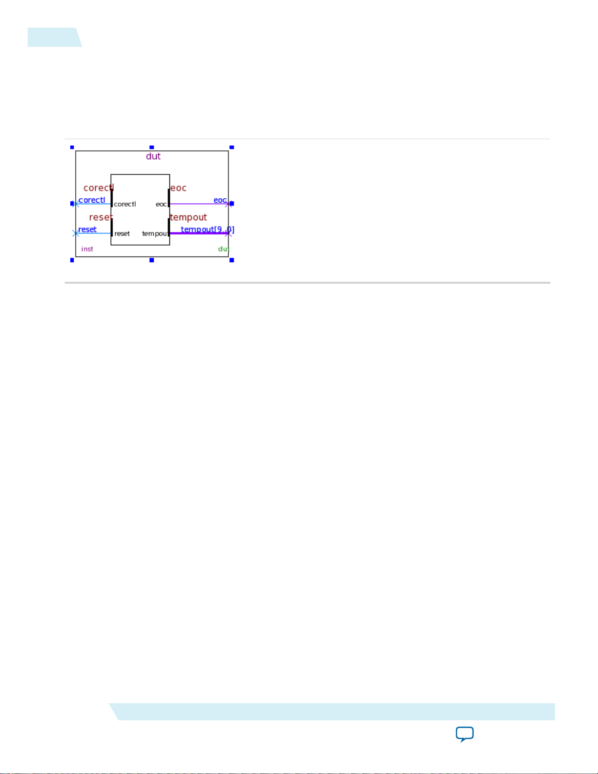
Figure 1: Altera Temperature Sensor IP Core Top-Level Diagram for Arria 10 Devices
The following lists the features for Altera Temperature Sensor IP core for Arria 10 devices:
UG-01074
2015.05.04
• For Arria 10 devices, the Altera Temperature Sensor IP core supports the instantiation of temperature
sensor block in your design from the IP Catalog.
• The Arria 10 temperature sensor block runs at 1 MHz, where the clock signal is coming from the
internal oscillator. Within the block, 10-bit ADC circuitry is included for converting sensor’s reading
to digital output.
• The corectl signal is used as an enable signal. When asserting the corectl signal, the ADC starts the
conversion and 10-bit data is available at tempout after 1,024 clock cycles. The eoc signal goes high for
one clock cycle indicating end of conversion. You can latch the data on tempout at the falling edge of
eoc.
• You can reset the temperature sensor anytime by asserting the reset signal.
Related Information
Transfer Function for Internal TSD
Provides more information on how to calculate the temperature from the tempout[9:0] value.
Altera Corporation
Altera Temperature Sensor IP Core User Guide
Send Feedback
Page 3
ce
tsdcalo[7:0]
clr
tsdcaldone
clk
Altera Temperature Sensor IP Core
TEMPERATURE
SENSOR
adcclk
CLOCK
DIVIDER
ADC
oe
UG-01074
2015.05.04
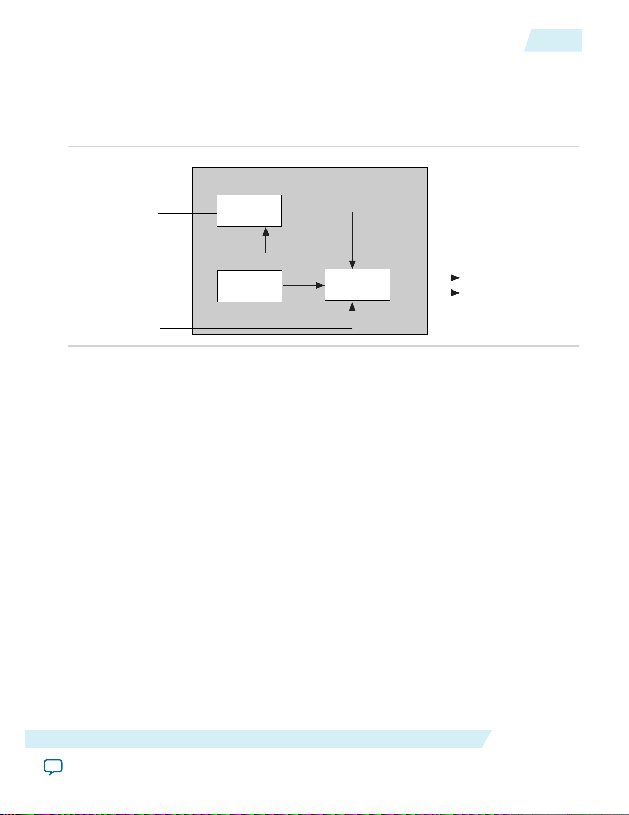
Temperature Sensing Operation for Arria V, Arria V GZ, Stratix IV, and Stratix V
Temperature Sensing Operation for Arria V, Arria V GZ, Stratix IV, and Stratix V Devices
Figure 2: Altera Temperature Sensor Block Diagram
This figure shows the top-level ports and the basic building blocks of the Altera Temperature Sensor IP
core.
3
Devices
The Altera Temperature Sensor IP core runs at the frequency of the clk signal. The clk signal can run at a
frequency of 80 MHz and below. The clock divider divides the clk signal to 1 MHz or less to feed the
ADC. You can set the value of the clock divider using the Altera Temperature Sensor IP core parameter
editor.
The ce signal connects to the output enable (oe) port of the clock divider block. Assert the ce signal to
enable the Altera Temperature Sensor IP core. When you deassert the ce signal, the IP core disables the
ADC, and maintains the previous values of the tsdcalo[7..0] and tsdcaldone signals unless you assert
the clr signal, or reset the device. The clr signal is asynchronous, and you must assert the clr signal at
least one clock cycle of the adcclk signal to clear the output ports.
Enabling the ADC allows you to measure the device temperature only once. To perform another tempera‐
ture measurement, assert the clr signal, or reset the device. The clr signal is asynchronous, and you must
assert the clr signal at least one clock cycle of the ADC clk signal to clear the output ports.
Note:
When you choose not to create the ce port, the IP core connects the ce port to VCC. In this case,
the ADC circuitry is always enabled. Altera recommends that you disable the ADC by deasserting
the ce signal when the ADC is not in use to reduce power consumption.
During device power-up or when you assert the asynchronous clr signal, the Altera Temperature Sensor
IP core sets the tsdcaldone port to 0 and the tsdcalo[7:0] signal to 11010101 or 0xD5. After 10 clock
cycles of the adcclk signal, the Altera Temperature Sensor IP core asserts the tsdcaldone signal to
indicate that the temperature sensing operation is complete and that the value of the tsdcalo[7:0] signal
is valid. The value of the tsdcalo[7:0] signal corresponds to the device temperature range. For more
information about the value of tsdcalo[7:0] signals, refer to the Related Information. To start another
temperature sensing operation, assert the clr signal for at least one clock cycle of the adcclk signal, or
reset the device.
Altera Temperature Sensor IP Core User Guide
Send Feedback
Altera Corporation
Page 4

4
Generating the Altera Temperature Sensor IP
Note: When you choose not to create the clr port , the Altera Temperature Sensor IP core connects the
clr port to GND. In this case, you must reset the device to clear the output signals or start a
temperature sensing operation. Altera recommends that you generate the clr port if you are
planning to run the temperature sensing operation more than once.
If a derived PLL output clock is used to drive the Altera Temperature Sensor IP core, a minimum pulse
violation might occur. When using the Altera Temperature Sensor IP core, you must ensure the clock
applied must be less than or equal to 1 MHz. If you are using a higher frequency clock, the Altera
Temperature Sensor IP core allows you use the 40 or 80 clock divider to reduce the clock frequency to be
less than or equal to 1.0MHz.
Related Information
Altera Temperature Sensor Signals on page 8
Provides more information about the value of tsdcalo[7:0] that corresponds to the device temperature
range.
Generating the Altera Temperature Sensor IP
To generate the Altera Temperature Sensor IP core, follow these steps:
1. Open the alttemp_sense_ex1.zip file and extract alttemp_sense_ex1.qar.
2. In the Quartus II software, open the alttemp_sense_ex1.qar file and restore the archive file into your
working directory.
3. On the IP Catalog window, search and click Altera Temperature Sensor.
4. In the New IP Instance dialog box, type tsd_s4 as your top-level file name.
5. In the Device family field, select Stratix IV.
6. Then, select your FPGA device family from the Device Family pull-down list. Click OK.
7. In the Parameter Editor, set the following parameter settings.
UG-01074
2015.05.04
Table 2: Configuration Settings for the Altera Temperature Sensor IP Core
Option Value
What is the input frequency? 40 MHz
What is the clock divider value? 80 MHz
Create a clock enable port Turned on
Create an asynchronous clear port Turned on
8.
Click Finish. The tsd_s4 module is built.
Compiling the Altera Temperature Sensor IP
To compile the Altera Temperature Sensor IP core in the Quartus II software, follow these steps:
1. Open the top-level file alttemp_sense_ex1.bdf in the Quartus II Block Editor software. This file
contains the input and output assignments and a placeholder for the tsd_s4 module.
2. To insert the tsd_s4 module, double-click on the Block Editor window. The Symbol window appears.
3. Under Name, browse to the tsd_s4.bsf file.
4. Click OK.
5. Place the tsd_s4 module onto the INSERT TSD_S4 BLOCK HERE placeholder so that the module
aligns with the input and output ports.
Altera Corporation
Altera Temperature Sensor IP Core User Guide
Send Feedback
Page 5

INPUT
VCC
clr
INPUT
VCC
clk
INPUT
VCC
ce
clr
clk
ce
tsd_s4
inst1
OUTPUT
tsdcalo[7..0]
OUTPUT
tsdcaldone
tsdcalo[7..0]
tsdcaldone
UG-01074
2015.05.04
Figure 3: Complete Design File
This figure shows the complete design file.
6. On the Processing menu, click Start Compilation.
7. When the Full Compilation was successful message box appears, click OK.
Using Clear Box Generator
You can use clear box generator, a command-line executable, to configure parameters that are in the
Altera Temperature Sensor IP core parameter editor. The clear box generator creates or modifies custom
IP core variations, which you can instantiate in a design file. The clear box generator generates IP core
variation file in Verilog HDL or VHDL format.
Using Clear Box Generator
5
Note:
Arria 10 Altera Temperature Sensor IP core does not support clear box generation format.
To generate the Altera Temperature Sensor IP core using the clear box generator, perform the following
steps:
1. Create a text file (.txt) that contains your clear box ports and parameter settings in your working
directory.
For example,
c:\altera\10.0\quartus\work\sample_param_test.txt.
This figure shows a sample text file to generate the Altera Temperature Sensor IP core.
Figure 4: Sample Text File for Clear Box Generator
Altera Temperature Sensor IP Core User Guide
Send Feedback
Altera Corporation
Page 6

6
Altera Temperature Sensor Device Support
UG-01074
2015.05.04
Note: Ensure that you enclose String-type values with double-quotes.
2. Access the command prompt of your operating system, and change the current directory to your
working directory by typing the following command:
cd c:\altera\10.0\quartus\work\
The clear box executable file name is clearbox.exe.
Note: When you install the Quartus II software, the %QUARTUS_ROOTDIR%\bin is added into
your system’s environment variables. Therefore, you can run the clear box command from any
directory.
3. To view the available ports and parameters for this IP core, type the following command at the
command prompt of your operating system:
clearbox alttemp_sense -h
4. To generate the Altera Temperature Sensor IP core variation file based on the ports and parameter
settings in the text file, type the following command:
clearbox alttemp_sense -f *.txt
For example, clearbox alttemp_sense -f sample_param_test.txt
5. After the clear box generator generates the IP core variation files, you can instantiate the IP core
module in a HDL file or a block diagram file in the Quartus II software.
6. To view the estimated hardware resources that the Altera Temperature Sensor IP core uses, type the
following command:
clearbox alttemp_sense -f sample_param_test.txt -resc_count
Note:
This command does not generate a HDL file.
Altera Temperature Sensor Device Support
The Altera Temperature Sensor IP core supports the following device family:
• Stratix V
• Stratix IV
• Arria 10
• Arria V
• Arria V GZ
Altera Temperature Sensor Parameters
The parameters are applicable for all supported devices except Arria 10 devices. There are no available
parameters for Arria 10 devices.
You can parameterize the Altera Temperature Sensor IP core using the IP Catalog and parameter editor,
or with the command-line interface (CLI). Use the parameter editor to quickly specify parameters in a
GUI.
Expert users may choose to instantiate and parameterize the IP core through the command-line interface
using the clear box generator command. This method requires you to have command-line scripting
knowledge.
Altera Corporation
Altera Temperature Sensor IP Core User Guide
Send Feedback
Page 7

UG-01074
2015.05.04
This table lists the parameter editor and CLI parameter settings for the Altera Temperature Sensor IP
core.
Table 3: Altera Temperature Sensor IP core Parameter Settings
Parameter CLI Parameter
Name Legal
Values
Name Legal
General Options Tab
Values
Altera Temperature Sensor Parameters
Description
7
What is the
input
frequency?
What is the
clock divider
value?
1.0 – 80.0
MHz
clk_frequency 1.0 – 80.0 Specifies the input frequency
of the clk signal. The input
frequency value is type string,
and the value must be less
than or equal to the clock
divider value.
The default value is 1.0
40, 80 clock_divider_value 40, 80 Specifies the clock divider
value. The IP core divides the
clock frequency value with the
clock divider value before
feeding the ADC. This option
is only enabled when the clk
signal frequency is more than
1 MHz.
Altera recommends clocking
the ADC with a 500 kHz
signal.
The CLI parameter is type
integer. Ensure that you
enable the clock divider by
setting the clock_divider_
enable parameter value to
on.
Create a clock
On/Off ce — Specifies whether to turn on
enable port
Altera Temperature Sensor IP Core User Guide
Send Feedback
The default value is 40.
the asynchronous clock enable
(ce) port.
Turn on this option when you
want to enable the Altera
Temperature Sensor IP core.
When you turn off this
option, the clock enable port
automatically connects to
VCC.
Altera Corporation
Page 8

8
Altera Temperature Sensor Signals
Parameter CLI Parameter
Name Legal
Values
Name Legal
Description
Values
UG-01074
2015.05.04
Create an
asynchronous
clear port
On/Off clr — Specifies whether to turn on
the asynchronous clear (clr)
port.
Turn on this option when you
want to reset the Altera
Temperature Sensor IP core.
When you turn off this
option, the clear port
automatically connects to
GND.
Altera Temperature Sensor Signals
The following tables list the Altera Temperature Sensor IP core signals.
Table 4: Altera Temperature Sensor IP Core Signals for Arria 10 Devices
Signals Direction Width (Bit) Description
corectl Input 1 Enables the temperature sensing feature by the IP
core.
reset Input 1 Resets the temperature sensing block.
tempout[9:0] Output 10 10-bit output data from internal ADC circuitry of
temperature sensor block.
eoc Output 1 Indicates end of internal ADC conversion. This
signal goes high for one clock cycles and you can
latch the data on tempout at the falling edge of EOC.
Table 5: Altera Temperature Sensor IP Core Signals for Suppported Devices
Signals Direction Width (Bit) Description
clk Input 1 Input clock signal that runs at a frequency of
80 MHz and below. The internal clock divider
reduces the frequency of the clk signal to 1 MHz or
less before clocking the ADC.
ce Input 1 The asynchronous clock enable signal for the clk
signal. This signal turns on/off the Altera Tempera‐
ture Sensor IP core that implements the TSD block.
This is an active-high signal. By default, this port
connects to VCC.
Altera Corporation
Altera Temperature Sensor IP Core User Guide
Send Feedback
Page 9

UG-01074
2015.05.04
Signals Direction Width (Bit) Description
clr Input 1 The asynchronous clear signal. When you assert the
clr signal, the IP core sets the tsdcalo[7:0] signal
Altera Temperature Sensor Signals
to 11010101 (0xD5) and the tsdcaldone signal to 0.
This is an active-high signal. By default, this port
connects to GND.
tsdcalo[7:0] Output 8 8-bit output signal that contains the analog-to-
digital-conversion temperature value. The 8-bit
value maps to a unique temperature value. During
device power-up or when you assert the clr signal,
the IP core sets the tsdcalo[7:0] to 11010101
(0xD5).
tsdcaldone Output 1 This signal indicates the completion of the tempera‐
ture sensing process. The IP core asserts this signal
when the process is complete. During device powerup or when you assert the clr signal, the IP core sets
the tsdcaldone to 0.
Table 6: The Mapping of tsdcalo [7..0] Value to Arria V, Arria V GZ, Stratix IV, and Stratix V Devices
Temperature
9
This table shows the value of tsdcalo[7:0] that corresponds to the device temperature range. The temperature
specification ranges from -70° C to 127° C.
Value of tsdcalo[7:0] in Hexadecimal Temperature in Degree Celsius (°C)
FF 127
... ...
E4 100
... ...
D5 85
... ...
D0 80
... ...
B2 50
... ...
9E 30
... ...
8A 10
... ...
80 0
... ...
76 -10
Altera Temperature Sensor IP Core User Guide
Send Feedback
Altera Corporation
Page 10

10
Altera Temperature Sensor Prototypes and Component Declarations
Value of tsdcalo[7:0] in Hexadecimal Temperature in Degree Celsius (°C)
... ...
6C -20
... ...
62 -30
... ...
4E -50
... ...
3A -70° C
Altera Temperature Sensor Prototypes and Component Declarations
Verilog HDL Prototype
UG-01074
2015.05.04
The Verilog HDL prototype is located in the <Quartus II installation directory>\eda\synthesis\ altera_mf.v
VHDL Component Declaration
The VHDL component declaration is located in the <Quartus II installation directory>\libraries\vhdl
\altera_mf\ directoryaltera_mf_components.vhd.
Document Revision History
This table lists the changes made to the document.
Table 7: Document Revision History
Date Document
Version
May 2015 2015.05.04
December 2014 2014.12.15
Changes Made
• Added a link on how to calculate the temperature from the
tempout[9:0] value.
• Editorial updates.
• Added Arria 10, Arria V, and Arria V GZ devices to the Device
Support section.
• Editorial changes to the warning message in Temperature
Sensing Operation section.
• Added Arria 10 devices information.
• Updated template.
Altera Corporation
Altera Temperature Sensor IP Core User Guide
Send Feedback
Page 11

UG-01074
2015.05.04
Document Revision History
11
Date Document
Version
June 2013 3.1
• Updated the “Temperature Sensing Operation” on page 3–1 to
Changes Made
clarify that enabling the ADC allows you to measure the
temperature of the device only once and to include a warning
about a minimum pulse violation when input clock derived
from a PLL.
• Updated “Features” on page 1–1 to notify that this IP core
does not provide simulation feature.
September 2010 3.0
• Updated the Parameter Settings chapter.
• Added the Prototypes and Component Declarations section.
• Added the Clear Box Generator chapter.
February 2010 2.0 Updated the Temperature Sensing Operation section.
November 2009 1.0 Initial release.
Altera Temperature Sensor IP Core User Guide
Send Feedback
Altera Corporation
 Loading...