

Page 1

Stratix V Avalon-ST Interface with SR-IOV PCIe Solutions
User Guide
Last updated for Altera Complete Design Suite: 14.1
Subscribe
Send Feedback
UG-01097_sriov
2014.12.15
101 Innovation Drive
San Jose, CA 95134
www.altera.com
Page 2
2014.12.15
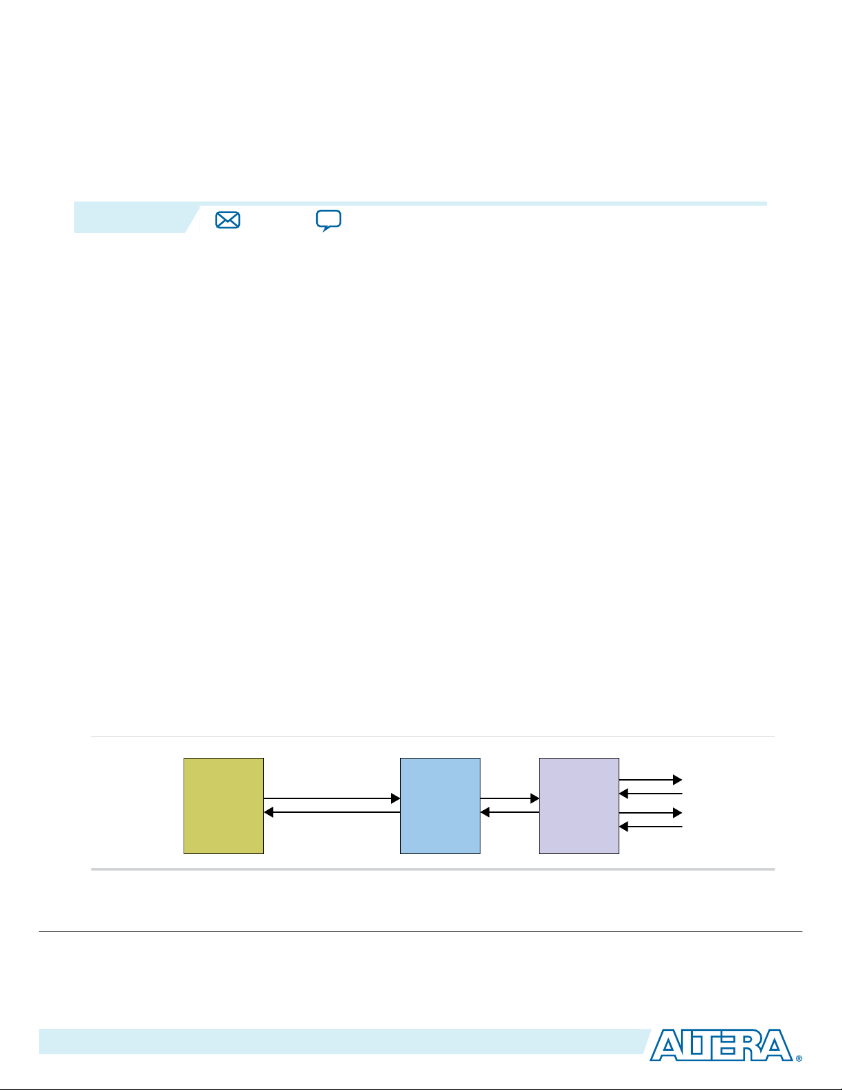
Application
Layer
(User Logic)
Avalon-ST
Interface
PCIe Hard IP
with SR-IOV
Block
PIPE
Interface
PHY IP Core
for PCIe
(PCS/PMA)
Serial Data
Transmission
www.altera.com
101 Innovation Drive, San Jose, CA 95134
Datasheet
1
UG-01097_sriov
Subscribe
Send Feedback
Stratix V Avalon-ST Interface with SR-IOV for PCIe Datasheet
Altera® Stratix® V FPGAs include a configurable, hardened protocol stack for PCI Express
compliant with PCI Express Base Specification 2.1 or 3.0. The Stratix V Hard IP for PCI Express with
Single Root I/O Virtualization (SR-IOV) IP core consists of this hardened protocol stack and the SR-IOV
soft logic. The SR-IOV soft logic uses Configuration Space Bypass mode to bypass the hardened Configu‐
ration Space. It implements the following functions in soft logic:
• Configuration Spaces for up to 2 PCIe Physical Functions (PFs) and a maximum of 128 Virtual
Functions (VFs) for both PFs
• BAR checking logic
• Support for the following interrupt types:
• MSI for PFs
• MSI-X for PFs and VFs
• Legacy interrupts for PFs
• Support for Advanced Error Reporting (AER) for PFs
• Support for Function Level Reset (FLR) for PFs and VFs
• Support for x2, x4, and x8 links using a 128- or 256-bit Avalon-ST datapath
®
that is
For details of the Configuration Space Bypass mode interface refer to the Configuration Space Bypass
Mode Interface Signals in the Stratix V Hard IP for PCI Express User Guide for the Avalon Streaming
Interface
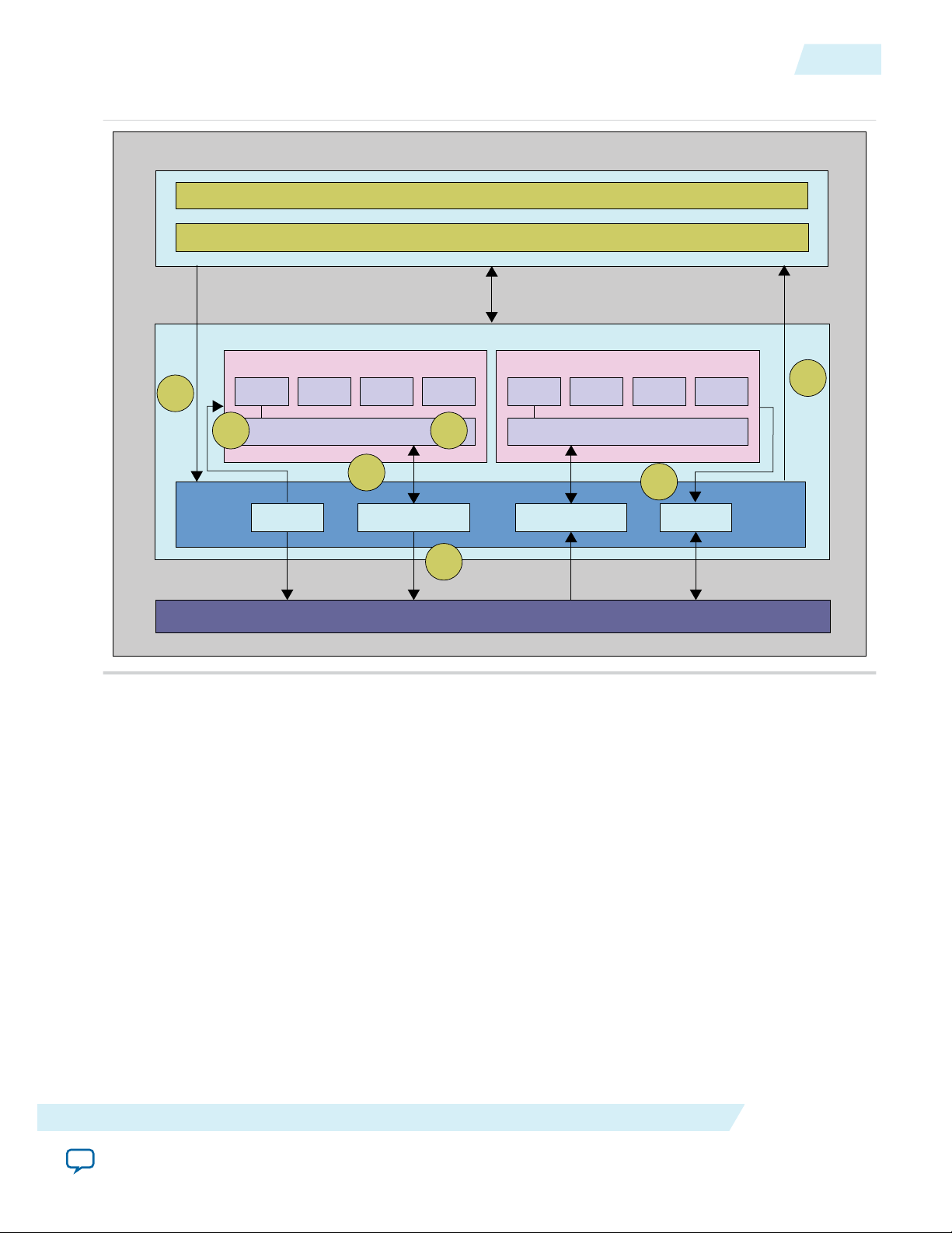
Figure 1-1: Stratix V PCIe Variant with SR-IOV
The following figure shows the high-level modules and connecting interfaces for this variant.
©
2014 Altera Corporation. All rights reserved. ALTERA, ARRIA, CYCLONE, ENPIRION, MAX, MEGACORE, NIOS, QUARTUS and STRATIX words and logos are
trademarks of Altera Corporation and registered in the U.S. Patent and Trademark Office and in other countries. All other words and logos identified as
trademarks or service marks are the property of their respective holders as described at www.altera.com/common/legal.html. Altera warrants performance
of its semiconductor products to current specifications in accordance with Altera's standard warranty, but reserves the right to make changes to any
products and services at any time without notice. Altera assumes no responsibility or liability arising out of the application or use of any information,
product, or service described herein except as expressly agreed to in writing by Altera. Altera customers are advised to obtain the latest version of device
specifications before relying on any published information and before placing orders for products or services.
ISO
9001:2008
Registered
Page 3

1-2
Features
UG-01097_sriov
2014.12.15
Table 1-1: PCI Express Data Throughput
The following table shows the aggregate bandwidth of a PCI Express link for Gen1, Gen2, and Gen3 for supported
link widths. The protocol specifies 2.5 giga-transfers per second for Gen1, 5.0 giga-transfers per second for Gen2,
and 8.0 giga-transfers per second for Gen3. This table provides bandwidths for a single transmit (TX) or receive
(RX) channel. The numbers double for duplex operation. Gen1 and Gen2 use 8B/10B encoding which introduces
a 20% overhead. In contrast, Gen3 uses 128b/130b encoding which reduces the data throughput lost to encoding
to less than 1%.
Link Width
×2 ×4 ×8
PCI Express Gen1 (2.5 Gbps) - 128-bit interface
PCI Express Gen2 (5.0 Gbps) - 128-bit interface
PCI Express Gen2 (5.0 Gbps) - 256-bit interface
N/A N/A
N/A
N/A N/A
PCI Express Gen3 (8.0 Gbps) - 128-bit interface 15.75 31.51
PCI Express Gen3 (8.0 Gbps) - 256-bit interface
Related Information
N/A N/A
• PCI Express Base Specification 2.1 or 3.0
• Single Root I/O Virtualization and Sharing Specification Revision 1.1.
• Stratix V Avalon-ST Interface for PCIe Solutions User Guide
• Creating a System with Qsys
Features
New features in the Quartus® II 14.1 software release:
• Reduced Quartus II compilation warnings by 50%.
16
16 32
32
N/A
63
The Stratix V Hard IP for PCI Express with SR-IOV supports the following features:
• Complete protocol stack including the Transaction, Data Link, and Physical Layers implemented as
• Support for ×2, ×4, and ×8 configurations with Gen1, Gen2, or Gen3 lane rates for Endpoints.
• Dedicated 16 KByte receive buffer.
• Optional hard reset controller for Gen2.
• Qsys example designs demonstrating parameterization, design modules, and connectivity.
• Extended credit allocation settings to better optimize the RX buffer space based on application type.
• End-to-end cyclic redundancy code (ECRC) generation and checking and advanced error reporting
Altera Corporation
hard IP.
Downtrains to appropriate configuration when plugged into a lower bandwidth configuration,
including Gen1 x1, Gen1 x2, and so on.
(AER) for high reliability applications.
Datasheet
Send Feedback
Page 4

UG-01097_sriov
2014.12.15
• Support for Configuration Space Bypass Mode, allowing you to design a custom Configuration Space
and support multiple functions.
• Support for Gen3 PIPE simulation.
• Easy to use:
• Flexible configuration.
• No license requirement.
• Example designs to get started.
Table 1-2: Feature Comparison for all Hard IP for PCI Express IP Cores
The table compares the features of the four Hard IP for PCI Express IP Cores.
Features
1-3
Feature Avalon‑ST Interface Avalon‑MM
Interface
Avalon‑MM DMA Avalon‑ST Interface with SR-
IP Core License Free Free Free Free
Native
Supported Supported Supported Supported
Endpoint
Legacy
Endpoint
(1)
Supported Not Supported Not Supported Not Supported
Root port Supported Supported Not Supported Not Supported
Gen1 ×1, ×2, ×4, ×8 ×1, ×2, ×4, ×8 Not Supported
Gen2 ×1, ×2, ×4, ×8 ×1, ×2, ×4, ×8 ×4, ×8
Gen3 ×1, ×2, ×4, ×8 ×1, ×2, ×4 ×4, ×8
64-bit Applica‐
Supported Supported Not supported Not supported
×8
×4, ×8
×2, ×4, ×8
tion Layer
interface
IOV
(1)
Datasheet
128-bit
Supported Supported Supported Supported
Application
Layer interface
256-bit
Supported Not Supported Supported Supported
Application
Layer interface
Not recommended for new designs.
Send Feedback
Altera Corporation
Page 5

1-4
Features
UG-01097_sriov
2014.12.15
Feature Avalon‑ST Interface Avalon‑MM
Interface
Transaction
Layer Packet
type (TLP)
• Memory Read
Request
• Memory Read
RequestLocked
• Memory Write
Request
• I/O Read
Request
• I/O Write
Request
• Configuration
Read Request
(Root Port)
• Configuration
Write Request
(Root Port)
• Message
Request
• Message
Request with
Data Payload
• Completion
Message
• Completion
with Data
• Memory Read
Request
• Memory Write
Request
• I/O Read
Request—Root
Port only
• I/O Write
Request—Root
Port only
• Configuration
Read Request
(Root Port)
• Configuration
Write Request
(Root Port)
• Completion
Message
• Completion
with Data
• Memory Read
Request (single
dword)
• Memory Write
Request (single
dword)
• Completion for
Locked Read
without Data
Avalon‑MM DMA Avalon‑ST Interface with SR-
IOV
• Memory Read
Request
• Memory Write
Request
• Completion
Message
• Completion
with Data
• Memory Read Request
• Memory Write
Request
• Configuration Read
Request (from Root
Port)
• Configuration Write
Request (from Root
Port)
• Message Request
• Completion Message
• Completion with Data
Payload size
Number of tags
supported for
non-posted
requests
62.5 MHz clock Supported Supported Not Supported Not Supported
Altera Corporation
128–2048 bytes 128–256 bytes 128, 256, 512 bytes 128–256 bytes
256 8 16 256
Datasheet
Send Feedback
Page 6

UG-01097_sriov
2014.12.15
Features
1-5
Feature Avalon‑ST Interface Avalon‑MM
Interface
Out-of-order
Not supported Supported Supported Not supported
completions
(transparent to
the Application
Layer)
Requests that
Not supported Supported Supported Supported
cross 4 KByte
address
boundary
(transparent to
the Application
Layer)
Polarity
Supported Supported Supported Supported
Inversion of
PIPE interface
signals
Avalon‑MM DMA Avalon‑ST Interface with SR-
IOV
ECRC
Supported Not supported Not supported Not supported
forwarding on
RX and TX
Number of MSI
requests
1, 2, 4, 8, 16, or 32 1, 2, 4, 8, 16, or 32 1, 2, 4, 8, 16, or 32 1, 2, 4, 8, 16, or 32 (for
Physical Functions)
MSI-X Supported Supported Supported Supported
Legacy
Supported Supported Supported Supported
interrupts
Expansion
Supported Not supported Not supported Not supported
ROM
The Stratix V Avalon-ST Interface with SR-IOV PCIe Solutions User Guide explains how to use this IP core
and not the PCI Express protocol. Although there is inevitable overlap between these two purposes, use
this document only in conjunction with an understanding of the PCI Express Base Specification.
Note:
This release provides separate user guides for the different variants. The Related Information
provides links to all versions.
Related Information
Datasheet
• Stratix V Avalon-MM Interface for PCIe Solutions User Guide
• Stratix V Avalon-ST Interface for PCIe Solutions User Guide
• Stratix V Avalon-ST Interface with SR-IOV for PCIe Solutions User Guide
Altera Corporation
Send Feedback
Page 7

1-6
Release Information
• V-Series Avalon-MM DMA Interface for PCIe Solutions User Guide
Release Information
Table 1-3: Hard IP for PCI Express Release Information
Item Description
Version 14.1
Release Date December 2014
Ordering Codes No ordering code is required
UG-01097_sriov
2014.12.15
Product IDs
Vendor ID
The Product ID and Vendor ID are not required
because this IP core does not require a license.
Device Family Support
Table 1-4: Device Family Support
Device Family Support
Stratix V Preliminary. The IP core is verified with prelimi‐
nary timing models for this device family. The IP
core meets all functional requirements, but might
still be undergoing timing analysis for the device
family. It can be used in production designs with
caution.
Other device families Refer to the Related Information below for other
device families:
Related Information
• Arria V Avalon-MM Interface for PCIe Solutions User Guide
• Arria V Avalon-ST Interface for PCIe Solutions User Guide
• Arria V GZ Avalon-MM Interface for PCIe Solutions User Guide
• Arria V GZ Avalon-ST Interface for PCIe Solutions User Guide
• Arria 10 Avalon-MM Interface for PCIe Solutions User Guide
• Arria 10 Avalon-MM DMA Interface for PCIe Solutions User Guide
• Arria 10 Avalon-ST Interface for PCIe Solutions User Guide
• Cyclone V Avalon-MM Interface for PCIe Solutions User Guide
• Cyclone V Avalon-ST Interface for PCIe Solutions User Guide
• IP Compiler for PCI Express User Guide
Altera Corporation
Datasheet
Send Feedback
Page 8

UG-01097_sriov
2014.12.15
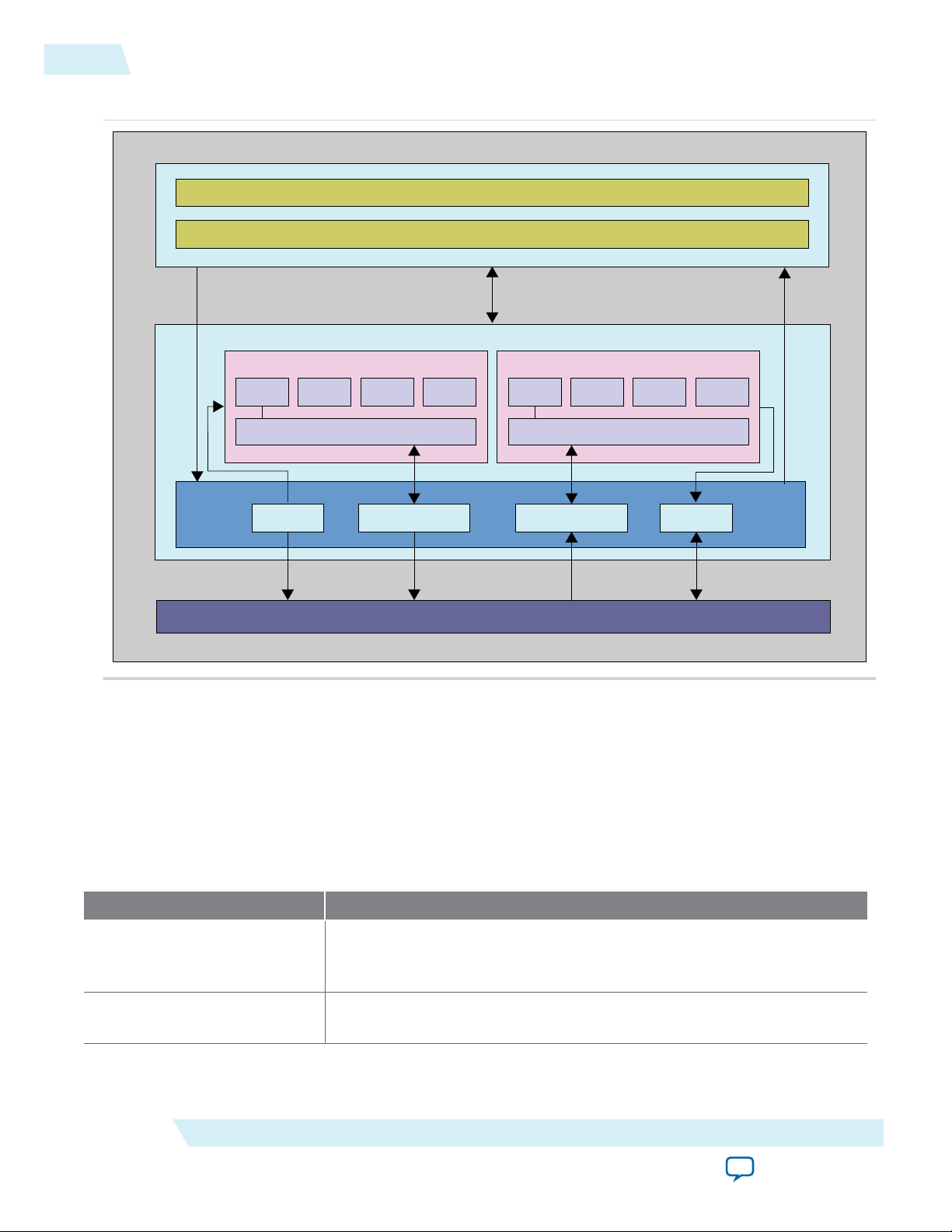
Example Designs
Altera provides example designs to familiarize you with the available functionality. Each design connects
the device under test (DUT) to an application programming platform (APP), labeled APPs in the figure
below. Certain critical parameters of the APPs component are set to match the values of the DUT. If you
change these parameters, you must change the APPs component to match. You can change the values for
all other parameters of the DUT without editing the APPs component.
In this example design, the following parameters must be set to match the values set in the DUT:
• Targeted Device Family
• Lanes
• Lane Rate
• Application Clock Rate
• Port type
• Application Interface
• Tags supported
• Maximum payload size
• Total PFs
• Total VFs
Example Designs
1-7
The following Qsys example designs are available for the Stratix V Hard IP for PCI Express with SR-IOV.
You can download them from the <install_dir>/ ip/altera/altera_pcie/altera_pcie_sriov/example_design/
directory:
• sriov_top_dma_gen2_x8_128b.qsys
• sriov_top_dma_gen2_x8_256b.qsys
• sriov_top_dma_gen3_x8_256b.qsys
• sriov_top_target_gen2_x8_256b_2pf.qsys
• sriov_top_target_gen3_x8_256b_1pf_32vf.qsys
• sriov_top_target_gen3_x8_256b_2pf_128vf.qsys
• sriov_top_target_gen3_x8_256b_2pf_4vf.qsys
• sriov_top_target_gen3_x8_256b_1pf_4vf_avmm.qsys
Related Information
Getting Started with the SR-IOV DMA Example Design on page 2-1
Debug Features
Debug features allow observation and control of the Hard IP for faster debugging of system-level
problems.
Related Information
Debugging on page 12-1
Datasheet
Altera Corporation
Send Feedback
Page 9

1-8
IP Core Verification
IP Core Verification
To ensure compliance with the PCI Express specification, Altera performs extensive verification. The
simulation environment uses multiple testbenches that consist of industry-standard bus functional
models (BFMs) driving the PCI Express link interface. Altera performs the following tests in the
simulation environment:
• Directed and pseudorandom stimuli are applied to test the Application Layer interface, Configuration
Space, and all types and sizes of TLPs
• Error injection tests that inject errors in the link, TLPs, and Data Link Layer Packets (DLLPs), and
check for the proper responses
• PCI-SIG® Compliance Checklist tests that specifically test the items in the checklist
• Random tests that test a wide range of traffic patterns
Altera provides the following two example designs that you can leverage to test your PCBs and complete
compliance base board testing (CBB testing) at PCI-SIG.
Related Information
• PCI SIG Gen3 x8 Merged Design - Stratix V
• PCI SIG Gen2 x8 Merged Design - Stratix V
UG-01097_sriov
2014.12.15
Compatibility Testing Environment
Altera has performed significant hardware testing to ensure a reliable solution. In addition, Altera
internally tests every release with motherboards and PCI Express switches from a variety of manufac‐
turers. All PCI-SIG compliance tests are run with each IP core release.
Performance and Resource Utilization
Because the PCIe protocol stack is implemented in hardened logic, it uses less than 1% of device
resources.
Table 1-5: Performance and Resource Utilization Stratix V Avalon-MM DMA for PCI Express
Number of PFs and VFs
2 PFs 2000 14 4800
1 PF, 4 VFs 3000 14 5450
1 PF, 32 VFs 3250 14 5950
2 PFs, 64 VFs 3650 14 6550
ALMs M20K Memory Blocks Logic Registers
2 PFs, 128 VFs 6450 14 9900
Note: Soft calibration of the transceiver module requires additional logic. The amount of logic required
Altera Corporation
depends upon the configuration.
Datasheet
Send Feedback
Page 10

UG-01097_sriov
2014.12.15
Related Information
Recommended Speed Grades
Fitter Resources Reports
Recommended Speed Grades
Table 1-6: Stratix V Recommended Speed Grades for All SR-IOV Configurations
Altera recommends setting the Quartus II Analysis & Synthesis Settings Optimization Technique to Speed when
the Application Layer clock frequency is 250 MHz. For information about optimizing synthesis, refer to “Setting
Up and Running Analysis and Synthesis in Quartus II Help. For more information about how to effect the
Optimization Technique settings, refer to Area and Timing Optimization in volume 2 of the Quartus II
Handbook. Refer to the Related Links below.
1-9
Link Rate Link Width Interface
Width
Application Clock
Frequency (MHz)
Recommended Speed Grades
Gen1 ×8 128 Bits 125 –1, –2, –3, –4
×4 128 bits 125 –1, –2, –3, –4
Gen2
×8 128 bits 250 –1, –2, –3
×8 256 bits 125 –1, –2, –3, –4
×2 128 bits 125 –1, –2, –3, –4
×4 128 bits 250 –1, –2, –3
Gen3
×4 256 bits 125 –1, –2, –3,–4
×8 256 bits 250 –1, –2, –3
Related Information
• Area and Timing Optimization
• Altera Software Installation and Licensing Manual
• Setting up and Running Analysis and Synthesis
(2)
(2)
(2)
Steps in Creating a Design for PCI Express
Before you begin
Select the PCIe variant that best meets your design requirements.
(2)
The -4 speed grade is also possible for this configuration; however, it requires significant effort by the end
user to close timing.
Datasheet
Send Feedback
Altera Corporation
Page 11

1-10
Steps in Creating a Design for PCI Express
UG-01097_sriov
2014.12.15
• Is your design an Endpoint or Root Port?
• What Generation do you intend to implement?
• What link width do you intend to implement?
• What bandwidth does your application require?
• Does your design require CvP?
1. Select parameters for that variant.
2. Simulate using an Altera-provided example design. All of Altera's PCI Express example designs are
available under <install_dir>/ip/altera/altera_pcie/. Alternatively, create a simulation model and use your
own custom or third-party BFM. The Qsys Generate menu generates simulation models. Altera
supports ModelSim®-Altera for all IP. The PCIe cores support the Aldec RivieraPro, Cadence NCsim,
Mentor Graphics ModelSim, and Synopsys VCS and VCS-MX simulators.
3. Compile your design using the Quartus II software. If the versions of your design and the Quartus II
software you are running do not match, regenerate your PCIe design.
4. Download your design to an Altera development board or your own PCB. Click on the All Develop‐
ment Kits link below for a list of Altera's development boards.
5. Test the hardware. You can use Altera's SignalTap® II Logic Analyzer or a third-party protocol
analyzer to observe behavior.
6. Substitute your Application Layer logic for the Application Layer logic in Altera's testbench. Then
repeat Steps 3–6. In Altera's testbenches, the PCIe core is typically called the DUT (device under test).
The Application Layer logic is typically called APPS.
Related Information
• Parameter Settings on page 3-1
• Getting Started with the SR-IOV DMA Example Design on page 2-1
• All Development Kits
Altera Corporation
Datasheet
Send Feedback
Page 12

Getting Started with the SR-IOV DMA Example
www.altera.com
101 Innovation Drive, San Jose, CA 95134
Design
2014.12.15
UG-01097_sriov
Subscribe
The SR-IOV example design consists of an SR-IOV bridge configured for one Physical Function (PF) and
four Virtual Functions (VFs). Each VF connects to a read DMA and a write DMA engine. The examples
design simulates the Transaction, Data Link, and Physical Layers using the Altera Root Port BFM. It also
supports Quartus II compilation.
The SR-IOV Qsys example design includes three Qsys subsystems. The top-level Qsys system comprises
the following components:
• DUT: This is the Stratix VHard IP for PCI Express with SR-IOV.
• APPs: This component is a Qsys subsystem that implements a highly efficient DMA engine. Each VF
has separate descriptor controllers for read DMA and write DMA descriptors. The read DMA and
write DMA routers arbitrate requests from the descriptor controllers. They forward the selected
request to the read DMA and write DMA modules. The read DMA transfers large blocks of data from
the Avalon-ST (SR-IOV) domain to the Avalon-MM (Qsys). The write DMA Write module transfers
large blocks of data from the Avalon-MM domain to the Avalon-ST domain. Refer to the SR-IOV
Example Design Block Diagram block diagram below.
In addition to high performance data transfer, the Read DMA and Write DMA modules ensure that
the requests on the PCI link adhere to the PCI Express Base Specification, 3.0. The read and write DMA
modules also perform the following functions:
Send Feedback
2
• Divide the original request into multiple requests to avoid crossing 4KByte boundaries.
• Divide the original request into multiple requests to ensure that the maximum payload size is equal
to or smaller than the maximum payload size for write.
• Divide the original request into multiple requests to ensure that the maximum read size is equal to
or smaller than the maximum read request size.
• Supports out-of-order completions when the original request is divided into multiple requests to
adhere to the maximum payload size.
• Altera PCIe Reconfig Driver IP Core: This Avalon-MM master drives the Transceiver Reconfiguration
Controller.
• Transceiver Reconfiguration Controller IP Core: The Transceiver Reconfiguration Controller
dynamically reconfigures analog settings to improve signal quality. For Gen1 and Gen2 data rates, the
Transceiver Reconfiguration performs offset cancellation and PLL calibration. For the Gen3 data rate,
the pcie_reconfig_driver_0 performs AEQ through the Transceiver Reconfiguration Controller.
©
2014 Altera Corporation. All rights reserved. ALTERA, ARRIA, CYCLONE, ENPIRION, MAX, MEGACORE, NIOS, QUARTUS and STRATIX words and logos are
trademarks of Altera Corporation and registered in the U.S. Patent and Trademark Office and in other countries. All other words and logos identified as
trademarks or service marks are the property of their respective holders as described at www.altera.com/common/legal.html. Altera warrants performance
of its semiconductor products to current specifications in accordance with Altera's standard warranty, but reserves the right to make changes to any
products and services at any time without notice. Altera assumes no responsibility or liability arising out of the application or use of any information,
product, or service described herein except as expressly agreed to in writing by Altera. Altera customers are advised to obtain the latest version of device
specifications before relying on any published information and before placing orders for products or services.
ISO
9001:2008
Registered
Page 13
Hard IP for PCI Express
SR-IOV Bridge
Rd_DC0 Rd_DC1 Rd_DC2 Rd_DC3
Read DMA Router
APPs - sriov_dma_app_g3x8_256b.qsys
sriov_top_dma_gen3_x8_256.qsys
rddc_ctl - rddc_ctl_256b.qsys wrdc_ctl - wrdc_ctl_256b.qsys
Wr_DC0 Wr_DC1 Wr_DC2 Wr_DC3
Write DMA Router
User Application Logic (On-Chip Memories)
DMA Write
TX Slave
RX Master DMA Read
2-2
Generating the Example Design Testbench
Figure 2-1: SR-IOV Example Design Block Diagram
UG-01097_sriov
2014.12.15
Related Information
Stratix V Hard IP for PCI Express User Guide for the Avalon Memory-Mapped Interface with DMA
Generating the Example Design Testbench
Follow these steps to generate the SR-IOV DMA example design testbench:
1. Copy <install_dir>/ ip/altera/altera_pcie/altera_pcie_sriov/example_design/sriov_top_dma_gen3_x8_256b.qsys
to your working directory. This top-level Qsys design includes three subsystems.
Altera Corporation
Qsys Subsystem Description
sriov_dma_app_g3x8_
256b.qsys
rddc_ctl_256b.qsys This subsystem implements the Read Descriptor Controller for 4 Read
This subsystem implements of the Read DMA read and Write DMA
modules and the Read and Write Descriptor Controllers. the DMA
engine.
DMA channels.
Getting Started with the SR-IOV DMA Example Design
Send Feedback
Page 14
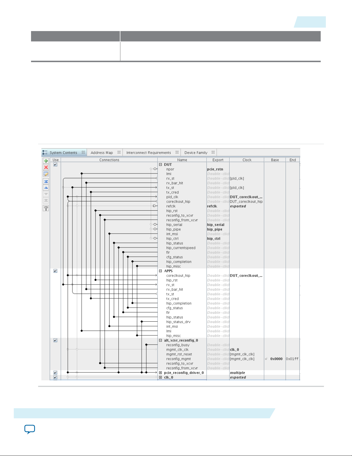
UG-01097_sriov
2014.12.15
wrdc_ctl_256b.qsys This subsystem implements the Write Descriptor Controller for 4 Write
Figure 2-2: Top-Level Qsys System for SR-IOV Gen3 x8 DMA Example Design
Generating the Example Design Testbench
Qsys Subsystem Description
DMA channels.
Note: File names that include 256b have a 256-bit interface to the Application Layer. File names that
include 128b have a 128-bit interface to the Application Layer.
2. Rename the top-level Qsys file, sriov_top_dma_gen3_x8_256b.qsys, to top.qsys.
3. In your working directory, start Qsys, by typing the following command:
qsys-edit
4. Open top.qsys.
The following figure shows the Qsys system.
2-3
5. On the Generate menu, select Generate Testbench System.
The Generation dialog box appears.
Getting Started with the SR-IOV DMA Example Design
Send Feedback
Altera Corporation
Page 15

2-4
Generating the Example Design Testbench
6. Specify the following parameters:
Table 2-1: Parameters to Specify on the Generation Menu in Qsys
Parameter Value
Testbench System
Create testbench Qsys system Standard, BFMs for standard Avalon interfaces
Create testbench simulation model Verilog. This option generates simulation files for
the testbench.
Allow mixed-language simulation Leave this option off.
Output Directory
UG-01097_sriov
2014.12.15
Path
Testbench
working_dir/
working_dir/testbench/
7. Click Generate.
Qsys generates the testbench.
8. To generate files for Quartus II compilation, on the Generate menu, select Generate HDL.
The Generation dialog box appears.
9. Specify the following parameters:
Table 2-2: Parameters to Specify on the Generation Menu in Qsys
Parameter Value
Verilog
Create HDL design files for synthesis Verilog.
Create timing and resource estimates for third-
Leave this option off.
party EDA synthesis tools
Create block symbol file (.bsf) Leave this option on.
Create simulation model.
Allow mixed language simulation.
Altera Corporation
Simulation
None . (You created the simulation model when
you generated the testbench.)
Leave this option off.
Output Directory
Getting Started with the SR-IOV DMA Example Design
Send Feedback
Page 16

UG-01097_sriov
2014.12.15
Understanding the Generated Files and Directories
Parameter Value
2-5
Path
working_dir/top
10.Click Generate.
11.On the File menu, click Save.
Understanding the Generated Files and Directories
Table 2-3: Qsys Generation Output Files
Directory Description
<testbench_dir>/<variant_name>/testbench
<testbench_dir>/<variant_name>/testbench/<cad_
vendor>
<testbench_dir>/<variant_name>/testbench/<variant_
name>_tb/simulation/submodules
Includes testbench subdirectories for the Aldec,
Cadence, Mentor, and Synopsys simulation tools
with the required libraries and simulation scripts.
Includes the HDL source files and scripts for the
simulation testbench.
Includes the HDL files for simulation.
Simulating the SR--IOV Example Design
Follow these steps to simulate the Qsys system using ModelSim:
1. In a terminal window, change to the <working_dir>/sim/mentor directory.
2. Start the ModelSim simulator by typing vsim.
3. To compile the simulation, type the following commands in the terminal window:
• do msim_setup.tcl (The msim_setup.tcl file defines aliases.
• ld_debug (The ld_debug command argument stops optimizations, improving visibility in the
ModelSim waveforms. )
• run -all
Running A Gate-Level Simulation
The PCI Express testbenches run simulations at the register transfer level (RTL). However, it is possible to
create you own gate-level simulations. Contact your Altera Sales Representative for instructions and an
example that illustrate how to create a gate-level simulation from the RTL testbench.
Getting Started with the SR-IOV DMA Example Design
Send Feedback
Altera Corporation
Page 17
Rd_DC0 Rd_DC1 Rd_DC2 Rd_DC3
Read DMA Router
APPs - sriov_dma_app_g3x8_256b.qsys
rddc_ctl - rddc_ctl_256b.qsys wrdc_ctl - wrdc_ctl_256b.qsys
Wr_DC0 Wr_DC1 Wr_DC2 Wr_DC3
Write DMA Router
DMA Write
TX Slave
RX Master DMA Read
1
3
2
4
Stratix V Hard IP for PCI Express
SR-IOV Bridge
User Application Logic (On-Chip Memories)
sriov_top_dma_gen3_x8_256.qsys
2-6
Understanding the DMA Functionality
Understanding the DMA Functionality
The following figures illustrate the DMA functionality using numbered steps.
Figure 2-3: Steps to Fetch Descriptor Table from Host Memory
UG-01097_sriov
2014.12.15
Fetching the Descriptor Table entries includes the following steps:
1. The host sets up descriptor controller register table using the RX master interface.
2. The Descriptor Controller instructs the DMA Read module to fetch the descriptor instruction entries.
3. The Host returns descriptor instruction entries to the Descriptor Controller.
4. In response to the Descriptor Controller instruction, the DMA Read drives a Memory Read Request to
the Hard IP.
Altera Corporation
Getting Started with the SR-IOV DMA Example Design
Send Feedback
Page 18
sriov_top_dma_gen3_x8_256.qsys
Hard IP for PCI Express
SR-IOV Bridge
Rd_DC0 Rd_DC1 Rd_DC2 Rd_DC3
Read DMA Router
APPs - sriov_dma_app_g3x8_256b.qsys
rddc_ctl - rddc_ctl_256b.qsys wrdc_ctl - wrdc_ctl_256b.qsys
Wr_DC0 Wr_DC1 Wr_DC2 Wr_DC3
Write DMA Router
User Application Logic (On-Chip Memories)
DMA Write
TX Slave
RX Master DMA Read
1
3
5
4
6
6
2, 6
UG-01097_sriov
2014.12.15
Figure 2-4: Steps To Perform a DMA Read
Understanding the DMA Functionality
2-7
The Read DMA operation includes the following steps:
1. The Descriptor Controller sends read descriptor instruction to initiate a DMA read.
2. The Descriptor Controller transmits a Memory Read TLP to the host starting at the source address.
3. The host returns DMA read data on the Avalon-ST interface.
4. The DMA Read Controller writes data to the destination address in the Application Layer memory.
5. The DMA Read module reports done status for each descriptor to the Descriptor Controller.
6. When all descriptors are complete, the Descriptor Controller sets the done bit of the last entry in the
descriptor table in host memory. The DMA Read Descriptor Controller sends this update to the TX
Slave. The TX Slave drives the update to the Hard IP for PCI Express.
Getting Started with the SR-IOV DMA Example Design
Send Feedback
Altera Corporation
Page 19
sriov_top_dma_gen3_x8_256.qsys
Stratix V Hard IP for PCI Express
SR-IOV Bridge
Rd_DC0 Rd_DC1 Rd_DC2 Rd_DC3
Read DMA Router
APPs - sriov_dma_app_g3x8_256b.qsys
rddc_ctl - rddc_ctl_256b.qsys wrdc_ctl - wrdc_ctl_256b.qsys
Wr_DC0 Wr_DC1 Wr_DC2 Wr_DC3
Write DMA Router
User Application Logic (On-Chip Memories)
DMA Write
TX Slave
RX Master DMA Read
1
3
5
4
2
2-8
Compiling the Example Design with the Quartus II Software
Figure 2-5: Steps To Perform a Write DMA
UG-01097_sriov
2014.12.15
The Write DMA operation includes the following steps:
1. The Descriptor Controller sends write descriptor instruction to initiate a DMA write.
2. The DMA Write reads data from the Application Layer memory.
3. Descriptor Controller transmits a Memory Write TLP to the host.
4. The DMA Write reports status for each descriptor to the Descriptor Controller.
5. When all descriptors are complete, the Descriptor Controller writes the ID of the last completed
descriptor to the EPLAST bit of the descriptor table.
Compiling the Example Design with the Quartus II Software
Complete the following steps to create and compile a Quartus II project.
1. In a terminal window, change to your working directory.
2. Copy the files from <install_dir>/ ip/altera/altera_pcie/altera_pcie_sriov/hw_devkit/ directory to your
working directory.
Altera Corporation
Getting Started with the SR-IOV DMA Example Design
Send Feedback
Page 20

UG-01097_sriov
2014.12.15
Using the IP Catalog To Generate Your Stratix V Hard IP for PCI Express as a Separate
Component
These files specify Synopsys Design Constraints, Quartus II design constraints, and top-level
connectivity.
3. On the Quartus II file menu, select the New Project Wizard.
a. Specify top_hw for the project name.
b. To specify design constraints, on the Tools menu, select Tcl Scripts.
The Tcl Script dialog box appears.
c. Scroll down to select top.tcl. Click run.
The Quartus II software runs the design constraints.
4. On the Processing menu, select Start compilation.
Quartus II compilation begins.
Using the IP Catalog To Generate Your Stratix V Hard IP for PCI Express as
a Separate Component
You can also instantiate the Stratix V Hard IP for PCI Express IP Core as a separate component for
integration into your project.
You can use the Quartus II IP Catalog and IP Parameter Editor to select, customize, and generate files
representing your custom IP variation. The IP Catalog (Tools > IP Catalog) automatically displays IP
cores available for your target device. Double-click any IP core name to launch the parameter editor and
generate files representing your IP variation.
2-9
For more information about the customizing and generating IP Cores refer to Specifying IP Core
Parameters and Options in Introduction to Altera IP Cores. For more information about upgrading older
IP cores to the current release, refer to Upgrading Outdated IP Cores in Introduction to Altera IP Cores.
Note:
Your design must include the Transceiver Reconfiguration Controller IP Core and the Altera PCIe
Reconfig Driver. Refer to the figure in the Qsys Design Flow section to learn how to connect this
components.
Related Information
• Introduction to Altera IP Cores
• Managing Quartus II Projects
Getting Started with the SR-IOV DMA Example Design
Send Feedback
Altera Corporation
Page 21

2014.12.15
www.altera.com
101 Innovation Drive, San Jose, CA 95134
Parameter Settings
3
UG-01097_sriov
Subscribe
Send Feedback
System Settings
Table 3-1: System Settings for PCI Express
Parameter Value Description
Lane Rate Gen1 (2.5 Gbps)
Gen2 (2.5/5.0 Gbps)
Gen3 (2.5/5.0/8.0
Gbps)
Number of Lanes ×1, ×2, ×4, ×8 Specifies the maximum number of lanes supported.
Port type Native Endpoint Specifies the port type. SR-IOV is only available for the Native
Specifies the maximum data rate at which the link can operate.
Endpoint in the current release.
The Endpoint stores parameters in the Type 0 Configuration
Space.
PCI Express Base
2.1, 3.0 Select either the 2.1 or 3.0 specification.
Specification
version
Application
interface
©
2014 Altera Corporation. All rights reserved. ALTERA, ARRIA, CYCLONE, ENPIRION, MAX, MEGACORE, NIOS, QUARTUS and STRATIX words and logos are
trademarks of Altera Corporation and registered in the U.S. Patent and Trademark Office and in other countries. All other words and logos identified as
trademarks or service marks are the property of their respective holders as described at www.altera.com/common/legal.html. Altera warrants performance
of its semiconductor products to current specifications in accordance with Altera's standard warranty, but reserves the right to make changes to any
products and services at any time without notice. Altera assumes no responsibility or liability arising out of the application or use of any information,
product, or service described herein except as expressly agreed to in writing by Altera. Altera customers are advised to obtain the latest version of device
specifications before relying on any published information and before placing orders for products or services.
Avalon-ST 256-bit
Avalon-ST 128-bit
This core supports either a 128- and 256-bit Avalon-ST
interface to the Application Layer.
ISO
9001:2008
Registered
Page 22

3-2
System Settings
Parameter Value Description
UG-01097_sriov
2014.12.15
Reference clock
frequency
RX Buffer credit
allocation performance for
received requests
100 MHz The PCI Express Base Specification 3.0 requires a
100 MHz ±300 ppm reference clock. The 125 MHz reference
clock is provided as a convenience for systems that include a
125 MHz clock source. For more information about Gen3
operation, refer to 4.3.8 Refclk Specifications for 8.0 GT/sin the
specification.
For Gen3, Altera recommends using a common reference
clock (0 ppm). For designs with separate reference clocks (non
0 ppm), the PCS occasionally must insert SKP symbols,
potentially causing the PCIe link to go to recovery. Gen1 and
Gen2 modes are not affected by this issue. Systems using the
common reference clock (0 ppm) are not affected by this issue.
The primary repercussion of this is a slight decrease in
bandwidth. On Gen3 x8 systems, this bandwidth impact is
negligible. If non 0 ppm mode is required, so that separate
reference clocks are being used, please contact Altera for
further information and guidance.
Minimum
Low
Balanced
High
Maximum
Determines the allocation of posted header credits, posted
data credits, non-posted header credits, completion header
credits, and completion data credits in the 16 KByte RX buffer.
The 5 settings allow you to adjust the credit allocation to
optimize your system. The credit allocation for the selected
setting displays in the message pane.
Refer to the Throughput Optimization chapter for more
information about optimizing performance. The Flow Control
chapter explains how the RX credit allocation and the
Maximum payload RX Buffer credit allocation and the
Maximum payload size that you choose affect the allocation
of flow control credits. You can set the Maximum payload
size parameter on the Device tab.
Altera Corporation
The Message window dynamically updates the number of
credits for Posted, Non-Posted Headers and Data, and
Completion Headers and Data as you change this selection.
Parameter Settings
Send Feedback
Page 23

UG-01097_sriov
2014.12.15
Parameter Value Description
• Minimum RX Buffer credit allocation—configures the
minimum PCIe specification allowed for non-posted and
posted request credits, leaving most of the RX Buffer space
for received completion header and data. Select this option
for variations where application logic generates many read
requests and only infrequently receives single requests
from the PCIe link.
• Low—configures a slightly larger amount of RX Buffer
space for non-posted and posted request credits, but still
dedicates most of the space for received completion header
and data. Select this option for variations where application
logic generates many read requests and infrequently
receives small bursts of requests from the PCIe link. This
option is recommended for typical endpoint applications
where most of the PCIe traffic is generated by a DMA
engine that is located in the endpoint application layer
logic.
• Balanced—configures approximately half the RX Buffer
space to received requests and the other half of the RX
Buffer space to received completions. Select this option for
variations where the received requests and received
completions are roughly equal.
• High—configures most of the RX Buffer space for received
requests and allocates a slightly larger than minimum
amount of space for received completions. Select this
option where most of the PCIe requests are generated by
the other end of the PCIe link and the local application
layer logic only infrequently generates a small burst of read
requests. This option is recommended for typical root port
applications where most of the PCIe traffic is generated by
DMA engines located in the endpoints.
• Maximum—configures the minimum PCIe specification
allowed amount of completion space, leaving most of the
RX Buffer space for received requests. Select this option
when most of the PCIe requests are generated by the other
end of the PCIe link and the local application layer logic
never or only infrequently generates single read requests.
This option is recommended for control and status
endpoint applications that don't generate any PCIe
requests of their own and only are the target of write and
read requests from the root complex.
System Settings
3-3
Parameter Settings
Send Feedback
Altera Corporation
Page 24

3-4
SR-IOV System Settings
Parameter Value Description
UG-01097_sriov
2014.12.15
Enable byte
On/Off When on, the RX and TX datapaths are parity protected.
parity ports on
Avalon-ST
interface
Enable credit
On/Off When on, the core includes the tx_cons_cred_sel port.
consumed
selection port tx_
cons_cred_sel
Enable Hard IP
On/Off
reset pulse at
power-up when
using the soft
reset controller
Related Information
PCI Express Base Specification 2.1 or 3.0
SR-IOV System Settings
Parity is odd.
This parameter is only available for the Avalon-ST Stratix V
Hard IP for PCI Express.
When On, the soft reset controller generates a pulse at power
up to reset the Hard IP. This pulse ensures that the Hard IP is
reset after programming the device, regardless of the behavior
of the dedicated PCI Express reset pin, perstn. This option is
available for Gen2 and Gen3 designs that use a soft reset
controller.
Parameter Value Description
Total active
1-2 This core supports 1 or 2 Physical Functions.
Physical
Functions (PFs) :
Total Physical
Function0
Virtual
Functions (PF0
VFs):
Total Physical
Function1
Virtual
Functions (PF1
VFs):
System
0-128 Total number of VFs for PF0. From 0-7 PFs are supported
when ARI is not supported. From 4–128 VFs are supported
when ARI is enabled. If PF1 is enabled, the sum of this field
and PF1 VFs should not exceed 128. When ARI is enabled, the
number of VFs should be a multiple of 4.
0-128 Total number of VFs for PF1. From 0-7 PFs are supported
when ARI is not supported. From 4–128 VFs are supported
when ARI is enabled. If PF1 is enabled, the sum of this field
and PF1 VFs should not exceed 128. When ARI is enabled, the
number of VFs should be a multiple of 4.
4KB - 4MB Specifies the pages sizes supported.
Supported Page
Size:
Altera Corporation
Parameter Settings
Send Feedback
Page 25

UG-01097_sriov
2014.12.15
Base Address Register (BAR) Settings
Parameter Value Description
3-5
Enable SR-IOV
On/Off
Turn this option on to include the SR-IOV functionality.
Support
Enable Alterna‐
tive Routing-ID
(ARI) support
On/Off
This core supports the following configurations:
• 1 PF and 4-7 VFs with no ARI
• 1 PF and 4-128 VFs in multiples of 4 with ARI
• 2 PFs with 4-6 VFs and no ARI
• 2 PFs with 4-128 VFs in multiples of 4 with ARI
Refer to Section 6.1.3 Alternative Routing-ID Interpretation
(ARI) of the PCI Express Base Specification more information
about ARI.
Enable
Functional Level
On/Off
When you turn this option on, each function can be individu‐
ally reset.
Reset (FLR)
Related Information
PCI Express Base Specification 2.1 or 3.0
Base Address Register (BAR) Settings
Each function can implement up to six BARs. You can configure up to six 32-bit BARs or three 64-bit
BARs for both PFs and VFs. The BAR settings are the same for all VFs associated with a PF.
Table 3-2: BAR Registers
Parameter Value Description
Present Enabled/Disabled Indicates whether or not this BAR is instantiated.
Type 32-bit address
64-bit address
If you select 64-bit address, 2 contiguous BARs are
combined to form a 64-bit BAR. you must set the
higher numbered BAR to Disabled.
If the BAR TYPE of any even BAR is set to 64-bit
memory, the next higher BAR supplies the upper
address bits. The supported combinations for 64-bit
BARs are {BAR1, BAR0}, {BAR3, BAR2}, {BAR4,
BAR5}.
Parameter Settings
Send Feedback
Altera Corporation
Page 26

3-6
Device Identification Registers
Parameter Value Description
UG-01097_sriov
2014.12.15
Prefetch‐
able
Prefetchable
Non-Prefetchable
Defining memory as prefetchable allows data in the
region to be fetched ahead anticipating that the
requestor may require more data from the same
region than was originally requested. If you specify
that a memory is prefetchable, it must have the
following 2 attributes:
• Reads do not have side effects
• Write merging is allowed
Size 16 Bytes–2 GBytes Specifies the memory size.
Device Identification Registers
Table 3-3: Device ID Registers
The following table lists the default values of the read-only Device ID registers. You can use the parameter editor
to change the values of these registers. At run time, you can change the values of these registers using the optional
reconfiguration block signals. You can specify Device ID registers for each Physical Function.
Register Name Range Default Value Description
Vendor ID 16 bits 0x00000000 Sets the read-only value of the Vendor ID register. This
parameter can not be set to 0xFFFF per the PCI Express
Specification.
Address offset: 0x000.
Device ID 16 bits 0x00000000 Sets the read-only value of the Device ID register.
Address offset: 0x000.
Revision ID 8 bits 0x00000000 Sets the read-only value of the Revision ID register.
Address offset: 0x008.
Class code 24 bits 0x00000000 Sets the read-only value of the Class Code register.
Address offset: 0x008.
Subsystem
Vendor ID
16 bits 0x00000000 Sets the read-only value of the Subsystem Vendor ID
register in the PCI Type 0 Configuration Space. This
parameter cannot be set to 0xFFFF per the PCI Express
Base Specification. This value is assigned by PCI-SIG to
the device manufacturer.
Address offset: 0x02C.
Altera Corporation
Parameter Settings
Send Feedback
Page 27

UG-01097_sriov
2014.12.15
Register Name Range Default Value Description
Interrupt Capabilities
3-7
Subsystem
Device ID
16 bits 0x00000000 Sets the read-only value of the Subsystem Device ID
register in the PCI Type 0 Configuration Space.
Address offset: 0x02C
Related Information
PCI Express Base Specification 2.1 or 3.0
Interrupt Capabilities
Table 3-4: MSI anad MSI-X Interrupt Settings
Each Physical Function defines its own MSI-X table settings. The VF MSI-X table settings are the same for all the
Virtual Functions associated with each Physical Function.
Parameter Value Description
MSI Interrupt Settings
PF0 MSI Requests 1,2,4,8,16,32
PF1 MSI Requests 1,2,4,8,16,32
Specifies the maximum number of MSI messages the Application
Layer can request. This value is reflected in Multiple Message
Capable field of the Message Control register, 0x050[31:16]. . For
MSI Interrupt Settings, if the PF MSI option is enabled, all PFs
support MSI capability.
MSI-X Interrupt Settings
PF MSI-X On/Off
When On, enables the MSI-X functionality. For PF and VF
MSI-X Interrupt Settings, if PF MSI-X is enabled, all PFs
VF MSI-X On/Off
supports MSI-X capability.
Bit Range
MSI-X Table size [10:0] System software reads this field to determine the MSI-X Table
size <n>, which is encoded as <n–1>. For example, a returned
value of 2047 indicates a table size of 2048. This field is readonly. Legal range is 0–2047 (211).
Address offset: 0x068[26:16]
MSI-X Table
Offset
[31:0] Specifies the offset from the BAR indicated in theMSI-X Table
BAR Indicator. The lower 3 bits of the table BAR indicator
(BIR) are set to zero by software to form a 32-bit qwordaligned offset
(1)
. This field is read-only.
Parameter Settings
Send Feedback
Altera Corporation
Page 28

3-8
PCI Express and PCI Capabilities Parameters
Parameter Value Description
UG-01097_sriov
2014.12.15
MSI-X Table
BAR Indicator
MSI-X Pending
Bit Array (PBA)
Offset
MSI-X PBA BAR
Indicator
PF0 Interrupt
Pin
PF1 Interrupt
Pin
[2:0] Specifies which one of a function’s BAR number. This field is
read-only. For 32-bit BARs, the legal range is 0–5. For 64-bit
BARs, the legal range is 0, 2, or 4.
[31:0] Points to the MSI-X Pending Bit Array table. It is offset from
the BAR value indicated in MSI-X Table BAR Indicator. The
lower 3 bits of the PBA BIR are set to zero by software to form
a 32-bit qword-aligned offset. This field is read-only.
[2:0] Specifies which BAR number contains the MSI-X PBA. For
32-bit BARs, the legal range is 0–5. For 64-bit BARs, the legal
range is 0, 2, or 4. This field is read-only.
Legacy Interrupts
inta–intd Applicable for PFs only to support legacy interrupts. When
enabled, the core receives interrupt indications from the
inta–intd
Application Layer on its INTA_IN, INTB_IN, INTC_IN and
INTD_IN inputs, and sends out Assert_INTx or Deassert_
INTx messages on the link in response to their activation or
deactivation, respectively.
You can configure the Physical Functions with separate
interrupt pins. Or, both functions can share a common
interrupt pin.
PF0 Interrupt
Line
0-255
Defines the input to the interrupt controller (IRQ0 - IRQ15)
in the Root Port that is activated by each Assert_INTx
PF1 Interrupt
0-255
message.
Line
Note:
1. Throughout this user guide, the terms word, dword and qword have the same meaning that they have
in the PCI Express Base Specification. A word is 16 bits, a dword is 32 bits, and a qword is 64 bits.
Related Information
PCI Express Base Specification Revision 2.1 or 3.0
PCI Express and PCI Capabilities Parameters
This group of parameters defines various capability properties of the IP core. Some of these parameters
are stored in the PCI Configuration Space - PCI Compatible Configuration Space. The byte offset
indicates the parameter address.
Altera Corporation
Parameter Settings
Send Feedback
Page 29

UG-01097_sriov
2014.12.15
Device Capabilities
Device Capabilities
3-9
Parameter Possible
Values
Maximum
128 bytes
payload size
256 bytes
Completion
timeout
range
ABCD
BCD
ABC
AB
B
A
None
Default
Value
Description
128 bytes Specifies the maximum payload size supported. This parameter
sets the read-only value of the max payload size supported field
of the Device Capabilities register (0x084[2:0]). Address: 0x084.
ABCD Indicates device function support for the optional completion
timeout programmability mechanism. This mechanism allows
system software to modify the completion timeout value. This
field is applicable only to Root Ports and Endpoints that issue
requests on their own behalf. Completion timeouts are
specified and enabled in the Device Control 2 register (0x0A8)
of the PCI Express Capability Structure Version. For all other
functions this field is reserved and must be hardwired to
0x0000b. Four time value ranges are defined:
• Range A: 50 us to 10 ms
• Range B: 10 ms to 250 ms
• Range C: 250 ms to 4 s
• Range D: 4 s to 64 s
Bits are set to show timeout value ranges supported. The
function must implement a timeout value in the range 50 s to
50 ms. The following values are used to specify the range:
Implement
completion
timeout
disable
• None—Completion timeout programming is not supported
• 0001 Range A
• 0010 Range B
• 0011 Ranges A and B
• 0110 Ranges B and C
• 0111 Ranges A, B, and C
• 1110 Ranges B, C and D
• 1111 Ranges A, B, C, and D
All other values are reserved. Altera recommends that the
completion timeout mechanism expire in no less than 10 ms.
On/Off On Disables the completion timeout mechanism. When On, the
core supports the completion timeout disable mechanism via
the PCI Express Device Control Register 2. The Applica‐
tion Layer logic must implement the actual completion timeout
mechanism for the required ranges. This option is forced to on
for PCI Express version 2.0 and higher Endpoints.
Parameter Settings
Send Feedback
Altera Corporation
Page 30

3-10
Error Reporting
UG-01097_sriov
2014.12.15
Parameter Possible
Values
Extended
On/Off On
tag support
Error Reporting
Parameter
Track Receive Completion Buffer
Overflow
Error Reporting
Table 3-5: Error Reporting
Default
Value
Description
When enabled, the Application Layer supports up to 256 tags
for non-posted requests. When disabled, the Application Layer
supports up to 32 tags. The Hard IP with SR-IOV support
disables tag checking. Consequently, the Application Layer
must implement Completion tag checking.
Possible
Values
On/Off
You can use this status bit as an additional check to
Description
complement the soft logic that tracks space in the RX
completion buffer. It is useful because the Endpoint RX
Completion buffer must advertise infinite credits for RX
Completions.
Parameter Value Default Value Description
Advanced
error
On/Off Off When On, enables the Advanced Error Reporting (AER)
capability.
reporting
(AER)
Enable
ECRC
checking
On/Off Off When On, enables ECRC checking. Sets the read-only
value of the ECRC check capable bit in the Advanced
Error Capabilities and Control Register. This
parameter requires you to enable the AER capability.
Enable
ECRC
generation
On/Off Off
When On, enables ECRC generation capability. Sets the
read-only value of the ECRC generation capable bit in
the Advanced Error Capabilities and Control
Register. This parameter requires you to enable the
AER capability.
Enable
ECRC
forwarding
on the
Avalon-ST
interface
On/Off Off When On, enables ECRC forwarding to the Application
Layer. On the Avalon-ST RX path, the incoming TLP
contains the ECRC dword
(1)
and the TD bit is set if an
ECRC exists. On the transmit the TLP from the Applica‐
tion Layer must contain the ECRC dword and have the
TD bit set.
Altera Corporation
Parameter Settings
Send Feedback
Page 31

UG-01097_sriov
2014.12.15
Parameter Value Default Value Description
Error Reporting
3-11
Track RX
completion
buffer
On/Off Off When On, the core includes the rxfx_cplbuf_ovf
output status signal to track the RX posted completion
buffer overflow status.
overflow on
the AvalonST interface
Note:
1. Throughout this user guide, the terms word, dword and qword have the same meaning that they have
in the PCI Express Base Specification. A word is 16 bits, a dword is 32 bits, and a qword is 64 bits.
Related Information
PCI Express Base Specification Revision 2.1 or 3.0
Error Reporting
Table 3-6: Error Reporting
Parameter Value Default Value Description
Track RX
Completion
Buffer
Overflow
On/Off Off When On, the core includes the rxfx_cplbuf_ovf
output status signal to track the RX posted completion
buffer overflow status.
Link Capabilities
Table 3-7: Link Capabilities
Parameter Value Description
Link port
number
Data link layer
active reporting
Parameter Settings
0x01 Sets the read-only value of the port number field in the Link
Capabilities register.
On/Off
Turn On this parameter for a downstream port, if the
component supports the optional capability of reporting the
DL_Active state of the Data Link Control and Management
State Machine. For a hot-plug capable downstream port (as
indicated by the Hot Plug Capable field of the Slot
Capabilities register), this parameter must be turned On.
For upstream ports and components that do not support this
optional capability, turn Off this option. This parameter is
only supported for the Stratix V Hard IP for PCI Express in
Root Port mode.
Altera Corporation
Send Feedback
Page 32

31 1 9 18 1 7 16 1 5 14
7
6 5
Physical Slot Number
No Command Completed Support
Electromechanical Interlock Present
Slot Power Limit Scale
Slot Power Limit Value
Hot-Plug Capable
Hot-Plug Surprise
Power Indicator Present
Attention Indicator Present
MRL Sensor Present
Power Controller Present
Attention Button Present
04 3 2 1
3-12
Slot Capabilities
Parameter Value Description
UG-01097_sriov
2014.12.15
Surprise down
reporting
On/Off
When this option is On, a downstream port supports the
optional capability of detecting and reporting the surprise
down error condition. This parameter is only supported for
the Stratix V Hard IP for PCI Express in Root Port mode.
Slot clock
configuration
On/Off When On, indicates that the Endpoint or Root Port uses the
same physical reference clock that the system provides on the
connector. When Off, the IP core uses an independent clock
regardless of the presence of a reference clock on the
connector.
Slot Capabilities
Table 3-8: Slot Capabilities
Parameter Value Description
Use Slot register On/Off The slot capability is required for Root Ports if a slot is implemented
on the port. Slot status is recorded in the PCI Express Capabili-
ties register. This parameter is only supported in Root Port mode.
Defines the characteristics of the slot. You turn on this option by
selecting Enable slot capability. The various bits are defined as
follows:
Altera Corporation
Parameter Settings
Send Feedback
Page 33

UG-01097_sriov
2014.12.15
Parameter Value Description
Power Management
3-13
Slot power scale
0–3
Specifies the scale used for the Slot power limit. The following
coefficients are defined:
• 0 = 1.0x
• 1 = 0.1x
• 2 = 0.01x
• 3 = 0.001x
The default value prior to hardware and firmware initialization is
b’00. Writes to this register also cause the port to send the Set_
Slot_Power_Limit Message.
Refer to Section 6.9 of the PCI Express Base Specification Revision for
more information.
Slot power limit
0–255
In combination with the Slot power scale value, specifies the upper
limit in watts on power supplied by the slot. Refer to Section 7.8.9 of
the PCI Express Base Specification for more information.
Slot number
Related Information
0-8191
Specifies the slot number.
PCI Express Base Specification Revision 2.1 or 3.0
Power Management
Table 3-9: Power Management Parameters
Parameter Value Description
Endpoint L0s
acceptable
latency
Maximum of 64 ns
Maximum of 128 ns
Maximum of 256 ns
Maximum of 512 ns
Maximum of 1 us
Maximum of 2 us
Maximum of 4 us
No limit
This design parameter specifies the maximum acceptable
latency that the device can tolerate to exit the L0s state for any
links between the device and the root complex. It sets the
read-only value of the Endpoint L0s acceptable latency field of
the Device Capabilities Register (0x084).
This Endpoint does not support the L0s or L1 states. However,
in a switched system there may be links connected to switches
that have L0s and L1 enabled. This parameter is set to allow
system configuration software to read the acceptable latencies
for all devices in the system and the exit latencies for each link
to determine which links can enable Active State Power
Management (ASPM). This setting is disabled for Root Ports.
The default value of this parameter is 64 ns. This is the safest
setting for most designs.
Parameter Settings
Send Feedback
Altera Corporation
Page 34

3-14
PHY Characteristics
Parameter Value Description
UG-01097_sriov
2014.12.15
Endpoint L1
Maximum of 1 us
acceptable
latency
Maximum of 2 us
Maximum of 4 us
Maximum of 8 us
Maximum of 16 us
Maximum of 32 us
No limit
PHY Characteristics
Table 3-10: PHY Characteristics
This value indicates the acceptable latency that an Endpoint
can withstand in the transition from the L1 to L0 state. It is an
indirect measure of the Endpoint’s internal buffering. It sets
the read-only value of the Endpoint L1 acceptable latency field
of the Device Capabilities Register.
This Endpoint does not support the L0s or L1 states. However,
a switched system may include links connected to switches
that have L0s and L1 enabled. This parameter is set to allow
system configuration software to read the acceptable latencies
for all devices in the system and the exit latencies for each link
to determine which links can enable Active State Power
Management (ASPM). This setting is disabled for Root Ports.
The default value of this parameter is 1 µs. This is the safest
setting for most designs.
Parameter Value Description
Gen2 transmit
deemphasis
3.5dB
6dB
Specifies the transmit de-emphasis for Gen2. Altera
recommends the following settings:
• 3.5dB: Short PCB traces
• 6.0dB: Long PCB traces.
Use ATX PLL On/Off When enabled, the Hard IP for PCI Express uses the ATX PLL
instead of the CMU PLL Using the ATX PLL instead of the
CMU PLL reduces the number of transceiver channels that are
necessary for Gen1 and Gen2 variants. This option requires
the use of the soft reset controller and does not support the
CvP flow. For more information about channel placement,
refer to Serial Data Signals on page 4-30.
Enable Common
Clock Configura‐
tion (for lower
latency)
On/Off When you turn this option on, the Application Layer and
Transaction Layer use a common clock. Using a common
clock reduces datapath latency because synchronizers are not
necessary.
This parameter is only available for the Avalon-ST interface.
Altera Corporation
Parameter Settings
Send Feedback
Page 35

UG-01097_sriov
2014.12.15
Simulation Options
Table 3-11: Simulation Options
Parameter Value Default Value Description
Simulation Options
3-15
Enable
DMA
Simulation
On/Off
On
Enable DMA simulation or target simulation. Set
Enable DMA Simulation on if your design includes the
SR-IOV DMA. Otherwise, simulation is for SR-IOV
target tests.
Parameter Settings
Send Feedback
Altera Corporation
Page 36

2014.12.15
tx_out0[<n>-1:0]
rx_in0[<n>-1:0]
Hard IP Serial
Hard IP Reset
Status
Hard IP for PCI Express with SR-IOV
flr_active_pf[<n>-1:0]
flr_active_vf[<n>-1:0]
flr_completed_pf[<n>-1:0]
refclk
coreclkout
pld_clk
flr_completed_vf[<n>-1:0]
cpl_err[6:0]
cpl_err_fn[7:0]
cpl_pending_pf[<n>-1:0]
cpl_pending_vf[<n>-1:0]
log_hdr[127:0]
tx_st_data[<n>-1:0]
tx_st_sop
tx_st_eop
tx_st_ready
tx_st_valid
tx_st_empty[1:0]
tx_st_err
bus_master_en_vf[<n>-1:0]
bus_master_en_pf[<n>-1:0]
bus_num_f0[7:0]
bus_num_f1[7:0]
device_num_f0[4:0]
device_num_f1[4:0]
max_payload_size[2:0]
mem_space_en_pf[<n>-1:0]
mem_space_en_vf[<n>-1:0]
pf0_num_vfs[7:0]
pf1_num_vfs[7:0]
rd_req_size[2:0]
Configuration
Status
TX Avalon-ST
TX Port
Component
Specific
TX Credit
RX Port
npor
pin_perst
Reset
Clocks
rx_st_data[<n>-1:0]
rx_st_sop
rx_st_eop
rx_st_ready
rx_st_valid
rx_st_empty[1:0]
rx_st_err
RX Avalon-ST
Component
Specific
RX BAR
Hit
rx_st_bar_hit_fn_tlp0[7:0]
rx_st_bar_hit_fn_tlp1[7:0]
rx_st_bar_hit_tlp0[7:0]
rx_st_bar_hit_tlp1[7:0]
rx_st_mask
tx_cred_datafccp[11:0]
tx_cred_datafcnp[11:0]
tx_cred_datafcp[11:0]
tx_cred_fchipcons[5:0]
tx_cred_fc_infinite[5:0]
tx_cred_hdrfccp[7:0]
tx_cred_hdrfcnp[7:0]
tx_cred_hdrfcp[7:0]
Function Level
Reset
Completion
Error Status
and Pending
Hard IP Control,
Miscellaneous &
Current Speed
test_in[31:0]
simu_mode_pipe
current_speed[1:0]
hpg_ctrler[4:0]
pld_clk_inuse
pld_core_ready
reset_status
serdes_pll_locked
testin_zero
reconfig_from_xcvr[<n>46-1:0]
reconfig_to_xcvr[<n>70-1:0]
Transceiver
Reconfiguration
LMI
lmi_dout[31:0]
lmi_func[8:0]
lmi_rden
lmi_wren
lmi_ack
app_int_sts_a
app_int_sts_b
app_int_sts_c
app_int_sts_d
app_int_ack
app_int_pend_status[1:0]
app_int_sts_fn
app_intx_disable[1:0]
lmi_addr[11:0]
lmi_din[31:0]
MSI
Interrupts
Select One
Interrupt
Mechanism
MSI-X
Interrupts
Legacy
Interrupts
app_msi_req
app_msi_req_fn[7:0]
app_msi_ack
app_msi_addr[127:0]
app_msi_data_pf[16<n>-1:0]
app_msi_enable_pf[1:0]
app_msi_mask_pf[32<n>-1:0]
app_msi_multi_msg_enable_pf[5:0]
app_msi_num[4:0]
app_msi_pending_bit_write_data
app_msi_pending_bit_write_en
app_msi_pending_pf[63:0]
app_msi_tc[2:0]
app_msi_status[1:0]
app_msix_req
app_msix_ack
app_msix_addr_pf[63:0]
app_msix_data[31:0]
app_msix_en_pf[1:0]
app_msix_en_vf[<n>-1:0]
app_msix_err
app_msix_fn_mask_pf[1:0]
app_msix_fn_mask_vf[<n>-1:0]
ko_clp_spc_data[11:0]
ko_cpl_spc_header[7:0]
nik1410905520092.image
www.altera.com
101 Innovation Drive, San Jose, CA 95134
Interfaces and Signal Descriptions
4
UG-01097_sriov
©
2014 Altera Corporation. All rights reserved. ALTERA, ARRIA, CYCLONE, ENPIRION, MAX, MEGACORE, NIOS, QUARTUS and STRATIX words and logos are
trademarks of Altera Corporation and registered in the U.S. Patent and Trademark Office and in other countries. All other words and logos identified as
trademarks or service marks are the property of their respective holders as described at www.altera.com/common/legal.html. Altera warrants performance
of its semiconductor products to current specifications in accordance with Altera's standard warranty, but reserves the right to make changes to any
products and services at any time without notice. Altera assumes no responsibility or liability arising out of the application or use of any information,
product, or service described herein except as expressly agreed to in writing by Altera. Altera customers are advised to obtain the latest version of device
specifications before relying on any published information and before placing orders for products or services.
Subscribe
Send Feedback
ISO
9001:2008
Registered
Page 37

4-2
Avalon-ST TX Interface
Avalon-ST TX Interface
Table 4-1: 128- or 256-Bit Avalon-ST TX Datapath
Signal Direction Description
UG-01097_sriov
2014.12.15
tx_st_data[<n>-1:0]
tx_st_sop
tx_st_eop
tx_st_ready
(3)
Output Indicates that the Transaction Layer is ready to accept data for
Input Data for transmission. Transmit data bus. When using a 128-bit
Avalon-ST bus, the width of tx_st_data is 128 bits. When using
a 256-bit Avalon-ST bus, the width of tx_st_data is 256 bits.
The Application Layer must provide a properly formatted TLP
on the TX interface. The mapping of message TLPs is the same as
the mapping of Transaction Layer TLPs with 4 dword headers.
The number of data cycles must be correct for the length and
address fields in the header. Issuing a packet with an incorrect
number of data cycles results in the TX interface hanging and
becoming unable to accept further requests.
<n> = 128 or 256.
Input Indicates first cycle of a TLP when asserted together with tx_st_
valid.
Input Indicates last cycle of a TLP when asserted together with tx_st_
valid.
transmission. The core deasserts this signal to throttle the data
stream. tx_st_ready may be asserted during reset. The Applica‐
tion Layer should wait at least 2 clock cycles after the reset is
released before issuing packets on the Avalon-ST TX interface.
The Application Layer can monitor the reset_status signal to
determine when the IP core has come out of reset.
(3)
To be Avalon-ST compliant, your Application Layer must have a readyLatency of 1 or 2 cycles.
Altera Corporation
If tx_st_ready is asserted by the Transaction Layer on cycle <n>
, then <n + readyLatency> is a ready cycle, during which the
Application Layer may assert valid and transfer data.
When tx_st_ready, tx_st_valid and tx_st_data are
registered (the typical case), Altera recommends a readyLa-
tency of 2 cycles to facilitate timing closure; however, a
readyLatency of 1 cycle is possible. If no other delays are added
to the read-valid latency, the resulting delay corresponds to a
readyLatency of 2.
Interfaces and Signal Descriptions
Send Feedback
Page 38

UG-01097_sriov
2014.12.15
Avalon-ST TX Interface
Signal Direction Description
4-3
tx_st_valid
tx_st_empty[1:0]
(3)
Input Clocks tx_st_data to the core when tx_st_ready is also
asserted. Between tx_st_sop and tx_st_eop, tx_st_valid must
not be deasserted in the middle of a TLP except in response to
tx_st_ready deassertion. When tx_st_ready deasserts, this
signal must deassert within 1 or 2 clock cycles. When tx_st_
ready reasserts, and tx_st_data is in mid-TLP, this signal must
reassert within 2 cycles. The figure entitled 64-Bit Transaction
Layer Backpressures the Application Layer illustrates the timing of
this signal.
To facilitate timing closure, Altera recommends that you register
both the tx_st_ready and tx_st_valid signals. If no other
delays are added to the ready-valid latency, the resulting delay
corresponds to a readyLatency of 2.
Input Indicates the number of qwords that are empty during cycles that
contain the end of a packet. When asserted, the empty dwords
are in the high-order bits. Valid only when tx_st_eop is asserted.
Not used when tx_st_data is 64 bits. For 128-bit data, only bit 0
applies and indicates whether the upper qword contains data. For
256-bit data, both bits are used to indicate the number of upper
words that contain data, resulting in the following encodings for
the 128-and 256-bit interfaces:
tx_st_err
128-Bit interface: tx_st_empty = 0, tx_st_data[127:0]contains
valid data tx_st_empty = 1, tx_st_data[63:0] contains valid
data.
256-bit interface:tx_st_empty = 0, tx_st_data[255:0] contains
valid datatx_ st_empty = 1, tx_st_data[191:0] contains valid
data tx_st_empty = 2, tx_st_data[127:0] contains valid data
tx_st_empty = 3, tx_st_data[63:0] contains valid data.
Input Indicates an error on transmitted TLP. This signal is used to
nullify a packet. It should only be applied to posted and
completion TLPs with payload. To nullify a packet, assert this
signal for 1 cycle after the SOP and before the EOP. When a
packet is nullified, the following packet should not be transmitted
until the next clock cycle. tx_st_err is not available for packets
that are 1 or 2 cycles long.
Refer to the figure entitled 128-Bit Avalon-ST tx_st_data Cycle
Definition for 3-Dword Header TLP with non-Qword Aligned
Address for a timing diagram that illustrates the use of the error
signal. Note that it must be asserted while the valid signal is
asserted.
Interfaces and Signal Descriptions
Send Feedback
Altera Corporation
Page 39

4-4
Avalon-ST TX Interface
Table 4-2: Component Specific TX Credit Signals
Signal Direction Description
UG-01097_sriov
2014.12.15
tx_cred_
datafccp[11:0]
tx_cred_
datafcnp[11:0]
tx_cred_datafcp[11:0]
tx_cred_
fchipcons[5:0]
Output Data credit limit for the received FC completions. Each credit is
16 bytes.
Output Data credit limit for the non-posted requests. Each credit is 16
bytes.
Output Data credit limit for the FC posted writes. Each credit is 16 bytes.
Output Asserted for 1 cycle each time the Hard IP consumes a credit.
These credits are from messages that the Hard IP for PCIe
generates for the following reasons:
• To respond to memory read requests
• To send error messages
This signal is not asserted when an Application Layer credit is
consumed. The Application Layer must keep track of its own
consumed credits. To calculate the total credits consumed, the
Application Layer must add its own credits consumed to those
consumed by the Hard IP for PCIe. The credit signals are valid
after dlup (data link up) is asserted.
The 6 bits of this vector correspond to the following 6 types of
credit types:
tx_cred_fc_
infinite[5:0]
• [5]: posted headers
• [4]: posted data
• [3]: non-posted header
• [2]: non-posted data
• [1]: completion header
• [0]: completion data
During a single cycle, the IP core can consume either a single
header credit or both a header and a data credit.
Output When asserted, indicates that the corresponding credit type has
infinite credits available and does not need to calculate credit
limits. The 6 bits of this vector correspond to the following 6
types of credit types:
• [5]: posted headers
• [4]: posted data
• [3]: non-posted header
• [2]: non-posted data
• [1]: completion header
• [0]: completion data
Altera Corporation
Interfaces and Signal Descriptions
Send Feedback
Page 40

UG-01097_sriov
2014.12.15
Avalon‑ST RX Interface
Signal Direction Description
4-5
tx_cred_hdrfccp[7:0]
Output Header credit limit for the FC completions. Each credit is 20
bytes.
tx_cred_hdrfcnp[7:0]
tx_cred_hdrfcp[7:0]
Output Header limit for the non-posted requests. Each credit is 20 bytes.
Output Header credit limit for the FC posted writes. Each credit is 20
bytes.
Avalon‑ST RX Interface
Table 4-3: 128- or 256‑Bit Avalon-ST RX Datapath
Signal Direction Description
rx_st_data[<n>-1:0]
Output Receive data bus. Refer to figures following this table for the
mapping of the Transaction Layer’s TLP information to rx_st_
data and examples of the timing of this interface. Note that the
position of the first payload dword depends on whether the TLP
address is qword aligned. The mapping of message TLPs is the
same as the mapping of TLPs with 4-dword headers. When using
a 128-bit Avalon-ST bus, the width of rx_st_data is 128. When
using a 256-bit Avalon-ST bus, the width of rx_st_data is 256
bits.
rx_st_sop
rx_st_eop Output Indicates that this is the last cycle of the TLP when rx_st_valid
rx_st_empty[1:0]
Interfaces and Signal Descriptions
Output
Indicates that this is the first cycle of the TLP when rx_st_valid
is asserted.
is asserted.
Output Indicates the number of empty qwords in rx_st_data. Valid
only when rx_st_eop is asserted in 128-bit and 256-bit modes.
For 128-bit data, only bit 0 applies; this bit indicates whether the
upper qword contains data. For 256-bit data single packet per
cycle mode, both bits are used to indicate whether 0-3 upper
Altera Corporation
Send Feedback
Page 41

4-6
Avalon‑ST RX Interface
Signal Direction Description
qwords contain data, resulting in the following encodings for the
128-and 256-bit interfaces:
• 128-Bit interface:
• rx_st_empty = 0, rx_st_data[127:0]contains valid data
• rx_st_empty = 1, rx_st_data[63:0] contains valid data
• 256-bit interface: single packet per cycle mode
• rx_st_empt y = 0, rx_st_data[255:0] contains valid
data
• rx_st_empty = 1, rx_st_data[191:0] contains valid data
• rx_st_empty = 2, rx_st_data[127:0] contains valid
data
• rx_st_empty = 3, rx_st_data[63:0] contains valid data
• When the TLP ends in the lower 128 bits, the following
equations apply:
• rx_st_eop[0]=1 & rx_st_empty[0]=0, rx_st_
data[127:0] contains valid data
• rx_st_eop[0]=1 & rx_st_empty[0]=1, rx_st_
data[63:0] contains valid data, rx_st_data[127:64] is
empty
• When TLP ends in the upper 128bits, the following equations
apply:
UG-01097_sriov
2014.12.15
• rx_st_ eop[1]=1 & rx_st_empty[1]=0, rx_st_
data[255:128] contains valid data
• rx_st_eop[1]=1 & rx_st_empty[1]=1, rx_st_
data[191:128] contains valid data, rx_st_
data[255:192] is empty
rx_st_ready
Input Indicates that the Application Layer is ready to accept data. The
Application Layer deasserts this signal to throttle the data stream.
If rx_st_ready is asserted by the Application Layer on cycle
<n> , then <n + > readyLatency is a ready cycle, during which
the Transaction Layer may assert valid and transfer data.
The RX interface supports a readyLatency of 2 cycles.
rx_st_valid Output Clocks rx_st_data into the Application Layer. Deasserts within
2 clocks of rx_st_ready deassertion and reasserts within 2 clocks
of rx_st_ready assertion if more data is available to send.
Altera Corporation
Interfaces and Signal Descriptions
Send Feedback
Page 42

UG-01097_sriov
2014.12.15
Avalon‑ST RX Interface
Signal Direction Description
4-7
rx_st_err
Related Information
Avalon Interface Specifications.
Output Indicates that there is an uncorrectable error correction coding
(ECC) error in the internal RX buffer. Active when ECC is
enabled. ECC is automatically enabled by the Quartus II
assembler. ECC corrects single-bit errors and detects double-bit
errors on a per byte basis.
When an uncorrectable ECC error is detected, rx_st_err is
asserted for at least 1 cycle while rx_st_valid is asserted.
Altera recommends resetting the Stratix V Hard IP for PCI
Express when an uncorrectable double-bit ECC error is detected.
Interfaces and Signal Descriptions
Send Feedback
Altera Corporation
Page 43

4-8
BAR Hit Signals
BAR Hit Signals
Signal Direction Description
UG-01097_sriov
2014.12.15
rx_st_bar_hit_
tlp0[7:0]
rx_st_bar_hit_
tlp1[7:0]
Output Identifies the matching BAR for the TLP driven on the Avalon-
ST RX interface. Valid for MRd, MWr and Atomic Op TLPs. rx_
st_bar_hit_tlp<n>[7:0] should be ignored for all other TLPs.
Valid in the first cycle of a TLP, when rx_st_valid_app and any
bit of rx_st_sop_app are asserted. rx_st_bar_hit_tlp0 applies
to the TLP that starts on bits [127:0] . rx_st_bar_hit_tlp1
applies to the TLP that starts on bits [255:128].
The following encodings are defined:
• 0x01: BAR 0 when configured as 32-bit BAR. Or BAR 0-1
when configured as 64-bit BAR.
• 0x02: BAR 1 when configured as 32-bit BAR. Reserved when
BAR 1 is combined with BAR 0 to form a 64-bit BAR.
• 0x04: BAR 2 when configured as 32-bit BAR. Or BAR 2-3
when configured as 64-bit BAR.
• 0x08: BAR 3 when configured as 32-bit BAR. Reserved when
BAR 2 is combined with BAR 3 to form a 64-bit BAR.
• 0x10: BAR4 when configured as 32-bit BAR. Or BAR 4-5
when configured as 64-bit BAR.
• 0x20: BAR5 when configured as 32-bit BAR. Reserved when
BAR 4 is combined with BAR 5 to form a 64-bit BAR.
• 0x40 and 0x80: Reserved.
When rx_st_bar_hit_tlp0 orrx_st_bar_hit_tlp1 indicates
the address of a PF, the BAR number above should be interpreted
as a PF BAR. When rx_st_bar_hit_tlp0 orrx_st_bar_hit_
tlp1provides the address of a VF (indicating a VF hit), the BAR
number should be interpreted as a VF BAR.
rx_st_bar_hit_fn_
tlp0[7:0]
rx_st_bar_hit_fn_
tlp1[7:0]
Altera Corporation
These signals are required to support multiple packets per cycle.
The SR-IOV implementation does not support multiple packets
per cycle. Consequently, these signals are not used.
output Identifies the Function number that was hit by a TLP driven on
the Avalon-ST RX interface. These outputs are valid for MRd,
MWr and Atomic Op TLPs. Theses and are to be ignored for all
other TLPs.
rx_st_bar_hit_fn_tlp<n> is valid in the first cycle of a TLP,
when rx_st_valid_app and any bit of rx_st_sop_app are
asserted. rx_st_bar_hit_fn_tlp0[7:0] applies to the TLP that
starts on bits [127:0]. rx_st_bar_hit_fn_tlp1[7:0] applies to
the TLP that starts on bits [255:128].
Interfaces and Signal Descriptions
Send Feedback
Page 44

UG-01097_sriov
2014.12.15
Configuration Status Interface
Signal Direction Description
4-9
rx_st_mask Input
The Application Layer asserts this signal to tell the Hard IP to
stop sending non-posted requests. This signal can be asserted at
any time. Up to 10 non-posted requests can be transferred to the
Application Layer after rx_st_mask is asserted.
Configuration Status Interface
The output signals listed below drive the settings of the various configuration register fields of the
Functions. These settings are often needed in designing Application Layer logic.
Table 4-4: Configuration Status Interface
Signal Direction Description
bus_num_f0[7:0] Output
Direction
Bus number assigned to Physical Function 0 by the Root
Complex, as captured from CfgWr transactions.
When ARI is enabled, the Application Layer must use this bus
number for all TLP requests and completions. When ARI is not
enabled, the Application Layer must use this bus number for TLP
requests and completions from PF0 and its associated Virtual
Functions.
bus_num_f1[7:0] Output Bus number assigned to Physical Function 1 by the Root
Complex, as captured from CfgWr transactions.
When ARI is enabled,bus_num_f1 is not used. When ARI is not
enabled, the application layer must use this bus number for TLP
requests and completions from PF1 and its associated Virtual
Functions.
device_num_f0[4:0] Output Device number assigned to Physical Function 0 by the Root
Complex, as captured from CfgWr transactions.
When ARI is enabled, the Requester ID only consists of bus
number and function number. Consequently, device_num_f0 is
unused. When ARI is disabled, the Application Layer must use
device_num_f0 for all TLP requests and completions from PF0
and its associated VFs.
device_num_f1[4:0] Output Device number assigned to Physical Function 1 by the Root
Complex, as captured from CfgWr transactions.
When ARI is enabled, the Requester ID only consists of bus
number and function number. Consequently, device_num_f1 is
unused. When ARI is disabled, the Application Layer must use
device_num_f1 for all TLP requests and completions from PF0
and its associated VFs.
Interfaces and Signal Descriptions
Send Feedback
Altera Corporation
Page 45

4-10
Completion Side Band Signals
Signal Direction Description
UG-01097_sriov
2014.12.15
mem_space_en_pf[<n>1:0]
bus_master_en_pf[<n>1:0]
mem_space_en_vf[<n>1:0]
bus_master_en_vf[<n>1:0]
Output The PF0 and PF1 PCI Command Registers drive the Memory
Space Enable bit.
Output ThePF0 and PF1 PCI Command Registers drive the Bus Master
Enable bit .
Output The PF0 and PF1 Control Registers drive the SR-IOV Memory
Space Enable bit.
Output The VF<n> Memory Space Enable bit of the PCI Command
Register drives bit <n> of this bus. <n> is the total number of
VFs.
Pf0_num_vfs[7:0] Output This output drives the value of the NumVFs register in the PF0 SR-
IOV Capability Structure.
Pf1_num_vfs[7:0] Output This output drives the value of the NumVFs register in the PF1 SR-
IOV Capability Structure .
max_payload_size[2:0] Output When only PF0 is present, the max payload size field of the PF0
PCI Express Device Control Register drives this output. When
two PFs are present, the minimum value of the max payload size
field of the PCI Express Device Control Registers drives this
output.
rd_req_size[2:0]
Output When only PF 0 is present, the max read request size field of PF0
PCI Express Device Control Register drives this output. When
two PFs are present, the minimum value of the max read request
size fields of the PCI Express Device Control Registers drives this
output.
Completion Side Band Signals
The following table describes the signals that comprise the completion side band signals for the AvalonST interface. The Stratix V Hard IP for PCI Express provides a completion error interface that the
Application Layer can use to report errors, such as programming model errors. When the Application
Layer detects an error, it can assert the appropriate cpl_err bit to indicate what kind of error to log. If
separate requests result in two errors, both are logged. The Hard IP sets the appropriate status bits for the
errors in the Configuration Space, and automatically sends error messages in accordance with the PCI
Express Base Specification. Note that the Application Layer is responsible for sending the completion with
the appropriate completion status value for non-posted requests. Refer to Error Handling on page 8-1
for information on errors that are automatically detected and handled by the Hard IP.
For a description of the completion rules, the completion header format, and completion status field
values, refer to Section 2.2.9 of the PCI Express Base Specification.
Altera Corporation
Interfaces and Signal Descriptions
Send Feedback
Page 46

UG-01097_sriov
2014.12.15
Table 4-5: Completion Signals for the Avalon-ST Interface
Completion Side Band Signals
4-11
Signal Directi
cpl_err[6:0]
Description
on
Input Completion error. This signal reports completion errors to the Configuration
Space. When an error occurs, the appropriate signal is asserted for one cycle.
• cpl_err[0]: Completion timeout error with recovery. This signal should
be asserted when a master-like interface has performed a non-posted
request that never receives a corresponding completion transaction after
the 50 ms timeout period when the error is correctable. The Hard IP
automatically generates an advisory error message that is sent to the Root
Complex.
• cpl_err[1]: Completion timeout error without recovery. This signal
should be asserted when a master-like interface has performed a nonposted request that never receives a corresponding completion transac‐
tion after the 50 ms time-out period when the error is not correctable. The
Hard IP automatically generates a non-advisory error message that is sent
to the Root Complex.
• cpl_err[2]: Completer abort error. The Application Layer asserts this
signal to respond to a non-posted request with a Completer Abort (CA)
completion. The Application Layer generates and sends a completion
packet with Completer Abort (CA) status to the requestor and then
asserts this error signal to the Hard IP. The Hard IP automatically sets the
error status bits in the Configuration Space register and sends error
messages in accordance with the PCI Express Base Specification.
• cpl_err[3]: Unexpected completion error. This signal must be asserted
when an Application Layer master block detects an unexpected
completion transaction. Many cases of unexpected completions are
detected and reported internally by the Transaction Layer. For a list of
these cases, refer to Transaction Layer Errors.
Interfaces and Signal Descriptions
Send Feedback
Altera Corporation
Page 47

4-12
Completion Side Band Signals
UG-01097_sriov
2014.12.15
Signal Directi
on
Description
• cpl_err[4]: Unsupported Request (UR) error for posted TLP. The
Application Layer asserts this signal to treat a posted request as an
Unsupported Request. The Hard IP automatically sets the error status bits
in the Configuration Space register and sends error messages in
accordance with the PCI Express Base Specification. Many cases of
Unsupported Requests are detected and reported internally by the
Transaction Layer. For a list of these cases, refer to Transaction Layer
Errors.
• cpl_err[5]: Unsupported Request error for non-posted TLP. The
Application Layer asserts this signal to respond to a non-posted request
with an Request (UR) completion. In this case, the Application Layer
sends a completion packet with the Unsupported Request status back to
the requestor, and asserts this error signal. The Hard IP automatically sets
the error status bits in the Configuration Space Register and sends error
messages in accordance with the PCI Express Base Specification. Many
cases of Unsupported Requests are detected and reported internally by the
Transaction Layer. For a list of these cases, refer to Transaction Layer
Errors.
• cpl_err[6]: Log header. If header logging is required, this bit must be set
in the every cycle in which any of cpl_err[2], cpl_err[3], cpl_err[4],
or cpl_err[5]is set.
cpl_err_
fn[7:0]
cpl_pending_
pf[1:0]
Input Specifies the function reporting the error on cpl_err[6:0].
Input
Completion pending. The Application Layer must assert this signal when a
master block associated with PF0 <n> is waiting for a completion. For
example, when a Non-Posted Request is pending from PF0. cpl_pending_
pf[0] records pending completions for PF0. cpl_pending_pf[1] records
pending completions for PF1.
cpl_pending_
vf[<n>-1:0]
Input Completion pending from VF. The Application Layer must keep bit <n>
asserted when the master block associated with Virtual Function <n> is
waiting for Completion. For example, when a Non-Posted transaction is
pending from VF <n>. <n> is the number of VFs.
log_hdr[127:0] Input When any of the bits 2, 3, 4, 5 of cpl_err is asserted, the Application Layer
may provide the header of the TLP that caused the error condition. The order
of bytes is the same as the order of the header bytes for the Avalon-ST
streaming interfaces.
ko_cpl_spc_
data[11:0]
Output The Application Layer can use this signal to build circuitry to prevent RX
buffer overflow for completion data. Endpoints must advertise infinite space
for completion data; however, RX buffer space is finite. ko_cpl_spc_data is
a static signal that reflects the total number of 16 byte completion data units
that can be stored in the completion RX buffer.
Altera Corporation
Interfaces and Signal Descriptions
Send Feedback
Page 48

UG-01097_sriov
2014.12.15
Clock Signals
4-13
Signal Directi
on
ko_cpl_spc_
header]7:0]
Output The Application Layer can use this signal to build circuitry to prevent RX
buffer overflow for completion headers. Endpoints must advertise infinite
space for completion headers; however, RX buffer space is finite. ko_cpl_
spc_header is a static signal that indicates the total number of completion
headers that can be stored in the RX buffer.
Related Information
PCI Express Base Specification Rev. 2.1 or 3.0
Clock Signals
Table 4-6: Clock Signals Hard IP Implementation
Signal Direction Description
refclk
Input Reference clock for the Stratix V Hard IP for PCI Express. It
must have the frequency specified under the System Settings
heading in the parameter editor.
Description
pld_clk
Input Clocks the Application Layer. You can drive this clock with
coreclkout_hip. If you drive pld_clk with another clock
source, it must be equal to or faster than coreclkout.
coreclkout
Output This is a fixed frequency clock used by the Data Link and
Transaction Layers. To meet PCI Express link bandwidth
constraints, this clock has minimum frequency requirements as
listed in coreclkout_hip Values for All Parameterizations in the
Reset and Clocks chapter .
Refer to Stratix V Hard IP for PCI Express Clock Domains in the Reset and Clocks chapter for more
information about clocks.
Function-Level Reset Interface
The function-level reset (FLR) interface can reset the individual SR-IOV functions.
Interfaces and Signal Descriptions
Send Feedback
Altera Corporation
Page 49

4-14
Interrupt Interface
Table 4-7: Function-Level Reset Interface
Signal Direction Description
UG-01097_sriov
2014.12.15
flr_active_pf[<n>1:0]
flr_completed_pf[<n>1:0]
flr_active_vf[<n>1:0]
Output When asserted, indicates the PF FLR field (bit 15) of the Device
Control Register is set. When asserted, a PF is being reset. (Bit 0
is for PF0. Bit 1 is for PF1).
The Application Layer must monitor flr_active_pf[<n>-1:0]
and clear any pending transactions associated with the function
being reset. The Application Layer must then assert flr_
completed_pf.
Input When asserted for one or more cycles, indicates that the Applica‐
tion Layer has completed resetting all the logic associated with
the PF. (Bit 0 is for PF0. Bit 1 is for PF1). When flr_active_pf
is asserted, the Application Layer must assert flr_completed
within 100 microseconds to re-enable the function.
Output Asserting bit <n> indicates a 1 was written into the FLR field (bit
15) of the Device Control Register for VF<n>. When asserted,
indicates that VF <n> is being reset. Multiple VFs can be reset
simultaneously. Consequently, the Application Layer must
monitor each bit of this output port in parallel.
The Application Layer must clear any pending transactions
associated with the VF being reset. It must then assert the
corresponding bit of flr_completed to signal to indicate it is
ready to re-enable the VF.
flr_completed_vf[<n>1:0]
Related Information
Function Level Reset (FLR) on page 6-5
Interrupt Interface
The SR-IOV Bridge supports MSI and MSI-X interrupts for both Physical and Virtual Functions. It also
supports legacy Interrupts for Physical Functions. The Application Layer can use this interface to generate
MSI or MSI-X interrupts from both PFs and VFs. The Application Layer can generate legacy interrupts
from PFs only. The Application Layer should select one of the three types of interrupts, depending on the
support provided by the platform and the software drivers. Ground the input pins for the unused
interrupt types.
<n> is the total number of VFs.
Input Asserting bit <n> for one or more cycles indicates that the
Application Layer has completed resetting all the logic associated
with VF <n>.
When flr_active_vf<n> is asserted, the Application Layer it
must assert the corresponding bit of flr_completed within 100
microseconds to re-enable the VF.
<n> is the total number of VFs.
Altera Corporation
Interfaces and Signal Descriptions
Send Feedback
Page 50

UG-01097_sriov
2014.12.15
This interface also includes signals to set and clear the individual bits in the MSI Pending Bit Register.
Table 4-8: MSI Interrupts
Signal Direction Description
app_msi_req Input When asserted, the Application Layer is requesting that an MSI
app_msi_req_fn[7:0] Input Specifies the function generating the MSI or MSI-X interrupt.
app_msi_ack Output Ack for MSI interrupts. When asserted, indicates that Hard IP
Interrupt Interface
4-15
interrupt be sent. Assertion causes an MSI posted write TLP to be
generated. The MSI TLP uses app_msi_req_fn[7:0], app_msi_
tc and app_msi_num to create the TLP. Refer to Figure 4-1 for a
timing diagram.
Driven in the same cycle as app_msi_req or app_msix_req.
has sent an MSI posted write TLP in response app_msi_req . The
Application Layer must wait for app_msi_ack after asserting
app_msi_req. The Application Layer must de-assert app_msi_
req for at least 1 cycle before signaling a new MSI interrupt.
app_msi_addr_
pf[127:0]
app_msi_data_pf[16<n>
-1:0]
app_msi_enable_
pf[1:0]
app_msi_mask_pf[32<n>
-1:0]
app_msi_multi_msg_
enable_pf[5:0]
Output
Output
Driven by the MSI address registers of PF0 and PF1. app_msi_
addr_pf[63:0] specifies the PF0 address. app_msi_addr_
pf[127:64] specifies the PF1 address.
Driven by the MSI Data Registers of PF0 and PF1. <n>= the
number of PFs.
Output Driven by the MSI Enable bit of the MSI Control Registers of PF0
and PF1.
Output
The MSI Mask Bits of the MSI Capability Structure drive app_
msi_mask_pf. This mask allows software to disable or defer
message sending on a per-vector basis. app_msi_mask_pf[31:0]
mask vectors for PF0.app_msi_mask_pf[63:32] mask vectors
for PF1.
Output Defines the number of interrupt vectors enabled for each PF. The
following encodings are defined:
• 3'b000: 1 vector
• 3'b001: 2 vectors
• 3'b010: 4 vectors
• 3'b100: 16 vectors
• 3'b101: 32 vectors
The MSI Multiple Message Enable field of the MSI Control
Register of PF0 drives app_msi_multi_msg_enable_pf[2:0].
The MSI Multiple Message Enable field of the MSI Control
Register of PF1 drives app_msi_multi_msg_enable_pf[5:3].
Interfaces and Signal Descriptions
Send Feedback
Altera Corporation
Page 51

4-16
Interrupt Interface
Signal Direction Description
app_msi_num[4:0] Input Identifies the MSI interrupt type to be generated. Provides the
low-order message data bits to be sent in the message data field
of MSI messages. Only bits that are enabled by the MSI Message
Control Register apply.
UG-01097_sriov
2014.12.15
app_msi_pending_bit_
write_data
Input Writes the MSI Pending Bit Register of the specified function
when msi_pending_bit_write_en is asserted. app_msi_
num[4:0] specifies the bit to be written. For more information
about the MSI Pending Bit Array (PBA), refer to Section 6.8.1.7
Mask Bits for MSI (Optional) in the PCI Local Bus Specification,
Revision 3.0. Refer to Figure 4-2 below.
msi_pending_bit_
write_en
Input Writes a 0 or 1 into selected bit position in the MSI Pending Bit
Register. app_msi_num[4:0] specifies the bit to be written. msi_
pending_bit_write_data specifies the data to be written (0 or
1). app_msi_req_fn specifies the function number.
msi_pending_bit_write_en cannot be asserted when app_msi_
req is high. Refer to Figure 4-2 below.
app_msi_pending_
pf[63:0]
app_msi_tc[2:0] Input Specifies the traffic class to be used to send the MSI or MSI-X
Output
The MSI Data Registers of PF0 and PF1 drive msi_pending_
pf[63:0]
posted write TLP. Must be valid when app_msi_req or app_
msix_req is asserted.
app_msi_status[1:0] Output
Indicates the status of an MSI request. Valid when app_msi_ack
is asserted. The following encodings are defined:
• 2'b00: MSI message sent
• 2'b01: MSI message is pending and not sent upstream because
the MSI mask was set. And, the Pending bit was set for the
MSI number.
• 2/b10: Requested aborted because of invalid parameters. Or,
request aborted because the MSI Enabled bit was not set in
the function's MSI Capability structure.
• 2'b11: Reserved.
Altera Corporation
Interfaces and Signal Descriptions
Send Feedback
Page 52

pld_clk
MSI Function No
MSI Number
Status
MSI TC
app_msi_req
app_msi_req_fn[7:0]
app_msi_num[4:0]
app_msi_tc[2:0]
app_msi_ack
MSI Data
app_msi_data_pf[15:0]
app_msi_status[1:0]
pld_clk
app_msi_req_fn[7:0]
MSI Function No.
MSI Data
app_msi_pending_bit_wr_data
app_msi_pending_bit_wr_en
MSI Vector
app_msi_num[4:0]
app_msi_data_pf[15:0]
UG-01097_sriov
2014.12.15
Figure 4-1: Timing Diagram for MSI Interrupt Generation
Figure 4-2: Timing Diagram for MSI Pending Bit Write Operation
The MSI Pending Bit Write Operation aborts the pending MSI interrupt.
Interrupt Interface
4-17
Table 4-9: MSI-X Interrupts
Interfaces and Signal Descriptions
Signal Direction Description
app_msix_req Input When asserted, the Application Layer is requesting that an MSI-
X interrupt be sent. Assertion causes an MSI-X posted write TLP
to be generated. The MSI-X TLP uses data from app_msi_req_
fn, app_msix_addr, app_msix_data, and app_msi_tc inputs.
Refer to Figure 4-3 below.
app_msix_ack Output Ack for MSI-X interrupts. When asserted, indicates that Hard IP
has sent an MSI-X posted write TLP in response app_msix_req .
The Application Layer must wait for after asserting app_msix_
req. The Application Layer must de-assert app_msix_req for at
least 1 cycle before signaling a new MSI interrupt.
Send Feedback
Altera Corporation
Page 53

4-18
Interrupt Interface
Signal Direction Description
app_msix_addr[63:0] Input The Application Layer drives the address for the MSI-X posted
write TLP on this input. Driven in the same cycle as app_msix_
req.
app_msix_data[31:0] Input The Application Layer drives app_msix_data[31:0] for the
MSI-X posted write TLP. Driven in the same cycle as app_msix_
req.
UG-01097_sriov
2014.12.15
app_msix_enable_
pf[1:0]
app_msix_enable_
vf[<n>-1:0]
app_msix_err
app_msix_fn_mask_
pf[1:0]
app_msix_fn_mask_
vf[<n>-1:0]
Output The MSI-X Enable bit of PF0 and PF1 MSI-X Control Register
drive this output.
Output The MSI-X Enable bit of the MSI-X Control Register for VF0
drives bit[0]. The MSI-X Enable bit of the MSI-X Control
Register for VF1 drives bit[1], and so on.
Output Indicates an error during the execution of an MSI-X request.
Valid when app_msix_ack is asserted. The following encodings
are defined:
• 1b'0: MSI-X message sent
• 1b'1: Error detected during execution of the MSI-X request.
No message sent. The following errors may occur:
• The function number is invalid
• The MSI-X Enable bit for the function was not set
• The MSI-X Function Mask was not set
Output The MSI-X Function Mask bit of PF0 and PF1 MSI-X Control
Register drive this output.
Output The MSI-X Function Mask bit of the MSI-X Control Register for
VF0 drives bit[0]. The MSI-X Function Mask bit of the MSI-X
Control Register for VF1 drives bit[1], and so on. <n> equals the
total number of VFs for both PF0 and PF1.
Altera Corporation
Interfaces and Signal Descriptions
Send Feedback
Page 54

pld_clk
MSI-X Function No
MSI-X Address
MSI-X TC
app_msix_req
app_msi_req_fn[7:0]
app_msix_addr[63:0]
app_msi_tc[2:0]
app_msix_ack
MSI-X Data
app_msix_data[31:0]
app_msi_status[1:0]
UG-01097_sriov
2014.12.15
Figure 4-3: Timing Diagram for MSI-X Interrupt Generation
Table 4-10: Legacy Interrupts
Signal Direction Description
Interrupt Interface
4-19
app_int_sts_a Input The Application Layer uses this signal to generate a legacy
INT<x>interrupt. <x> corresponds to a-d for functions
app_int_sts_b Input
app_int_sts_c Input
app_int_sts_d Input
programmed to use interrupt pins a-d. The Hard IP sends an
INTx_Assert message upstream to the Root Complex in
response to a low-to- high transition. The Hard IP sends a INTX_
Deassert in response to a high-to-low transition. The INTX_
Deassert message is only sent if a previous INTx_Assert
message was sent. Figure 4-4 and Figure 4-5 for timing
diagrams.
This input has no effect if the INT<x>Disable bit in the PCI
Command Register of the interrupting function is set to 1.
app_int_ack Output A pulse on this output indicates that an INTx_Assert or INTX_
Deassert message has been sent. Assertion is in response to a
transition on aapp_int_sts_<x> input. This signal is asserted for
at least 1 cycle when an INTx_Assert message TLP has been
transmitted. It is asserted when either of the following occurs:
• A low-to-high transition on one of the app_int_sts_<x>
inputs
• A INTX_Deassert message TLP has been transmitted in
response to a high-to-low transition
The Application Layer must wait for app_int_ack the after
making a transition on one of theapp_int_sts_<x> inputs,
before signaling a new transition.
Interfaces and Signal Descriptions
Send Feedback
Altera Corporation
Page 55

clk
app_int_sts_<x>
app_int_ack
clk
app_int_sts_<x>
app_int_ack
4-20
Implementing MSI-X Interrupts
Signal Direction Description
UG-01097_sriov
2014.12.15
app_int_pend_
status[1:0]
Input The Application Layer must drive each of these inputs with the
interrupt pending status of the corresponding PF. The Interrupt
Pending Status bit of the PCI Status Register records the pending
status .
app_int_sts_fn Input Identifies the function generating the legacy interrupt. When
app_int_sts_fn = 0, specifies status for PF0. When app_int_
sts_fn = 1, specifies status for PF1.
app_intx_disable[1:0] Output This output is driven by the INT<x>Disable bit of the PCI
Command Register of FP0 and PF1. app_intx_disable[0]
disables PF0. app_intx_disable[1] disables PF1.
Figure 4-4: Legacy Interrupt Assertion
Figure 4-5: Legacy Interrupt Deassertion
Related Information
• Programming and Testing SR-IOV Bridge MSI Interrupts on page 7-1
• PCI Local Bus Specification, Revision 3.0
Implementing MSI-X Interrupts
Section 6.8.2 of the PCI Local Bus Specification describes the MSI-X capability and table structures. The
MSI-X capability structure points to the MSI-X Table structure and MSI-X Pending Bit Array (PBA)
registers. The BIOS sets up the starting address offsets and BAR associated with the pointer to the starting
address of the MSI-X table and PBA registers.
The following figure shows the Application Layer modules that implement MSI-X interrupts.
Altera Corporation
Interfaces and Signal Descriptions
Send Feedback
Page 56

Host
RX
TX
RX
TX
PCIe with SR-IOV Bridge
MSI-X Table
IRQ
Processor
MSI-X PBA
IRQ Source
Application Layer
Host SW Programs Addr,
Data and Vector Control
Memory Write
TLP
Memory Write TLP
Monitor & Clr
Addr, Data
Vector Control
Vector Control
Vector Control
Vector Control
Message Data
Message Data
Message Data
Message Data
DWORD 3 DWORD 2
Message Upper Address
Message Upper Address
Message Upper Address
Message Upper Address
DWORD 1
Message Address
Message Address
Message Address
Message Address
DWORD 0 Host Byte Addresses
Entry 0
Entry 1
Entry 2
Entry (N - 1)
Base
Base + 1 × 16
Base + 2 × 16
Base + (N - 1) × 16
UG-01097_sriov
2014.12.15
Figure 4-6: MSI-X Interrupt Components
Implementing MSI-X Interrupts
4-21
1. Host software sets up the MSI-X interrupts in the Application Layer by completing the following steps:
a. Host software reads the Message Control register at 0x050 register to determine the MSI-X Table
size. The number of table entries is the <value read> + 1.
The maximum table size is 2048 entries. Each 16-byte entry is divided in 4 fields as shown in the
figure below. The MSI-X table can reside in any BAR. The base address of the MSI-X table must be
aligned to a 4 KByte boundary.
b. The host sets up the MSI-X table. It programs MSI-X address, data, and masks bits for each entry as
shown in the figure below.
Figure 4-7: Format of MSI-X Table
c. The host calculates the address of the <nth> entry using the following formula:
nth_address = base address[BAR] + 16<n>
2. When Application Layer has an interrupt, it drives an interrupt request to the IRQ Source module.
3. The IRQ Source sets appropriate bit in the MSI-X PBA table.
The PBA can use qword or dword accesses. For qword accesses, the IRQ Source calculates the address
of the <mth> bit using the following formulas:
qword address = <PBA base addr> + 8(floor(<m>/64))
qword bit = <m> mod 64
Interfaces and Signal Descriptions
Send Feedback
Altera Corporation
Page 57

Pending Bits 0 through 63
Pending Bits 64 through 127
Pending Bits ((N - 1) div 64) × 64 through N - 1
QWORD 0
QWORD 1
QWORD (( N - 1) div 64)
Base
AddressPending Bit Array (PBA)
Base + 1 × 8
Base + ((N - 1) div 64) × 8
Configuration Space
128 32-bit registers
(4 KBytes)
LMI
32
lmi_dout
lmi_ack
12
lmi_addr
9
lmi_func
32
lmi_din
lmi_rden
lmi_wren
pld_clk
Hard IP for PCIe
4-22
LMI Signals
Figure 4-8: MSI-X PBA Table
4. The IRQ Processor reads the entry in the MSI-X table.
a. If the interrupt is masked by the Vector_Control field of the MSI-X table, the interrupt remains in
the pending state.
b. If the interrupt is not masked, IRQ Processor sends Memory Write Request to the TX slave
interface. It uses the address and data from the MSI-X table. If
IRQ Processor creates a three-dword header. If the
dword header.
5. The host interrupt service routine detects the TLP as an interrupt and services it.
Related Information
Message Upper Address
Message Upper Address
UG-01097_sriov
2014.12.15
= 0, the
> 0, it creates a 4-
• Floor and ceiling functions
• PCI Local Bus Specification, Rev. 3.0
LMI Signals
LMI interface can write log error descriptor information in the TLP header log registers. The LMI access
to other registers is intended for debugging, not normal operation.
Figure 4-9: Local Management Interface
Altera Corporation
Interfaces and Signal Descriptions
Send Feedback
Page 58

UG-01097_sriov
2014.12.15
The LMI interface is synchronized to pld_clk and runs at frequencies up to 250 MHz. The LMI address is
the same as the Configuration Space address. The read and write data are always 32 bits. The LMI
interface provides the same access to Configuration Space registers as Configuration TLP requests.
Register bits have the same attributes, (read only, read/write, and so on) for accesses from the LMI
interface and from Configuration TLP requests.
When a LMI write has a timing conflict with configuration TLP access, the configuration TLP accesses
have higher priority. LMI writes are held and executed when configuration TLP accesses are no longer
pending. An acknowledge signal is sent back to the Application Layer when the execution is complete.
All LMI reads are also held and executed when no configuration TLP requests are pending. The LMI
interface supports two operations: local read and local write. The timing for these operations complies
with the Avalon-MM protocol described in the Avalon Interface Specifications. LMI reads can be issued at
any time to obtain the contents of any Configuration Space register. LMI write operations are not
recommended for use during normal operation. The Configuration Space registers are written by requests
received from the PCI Express link and there may be unintended consequences of conflicting updates
from the link and the LMI interface. LMI Write operations are provided for AER header logging, and
debugging purposes only.
Table 4-11: LMI Interface
Signal Direction Description
LMI Signals
4-23
lmi_dout[31:0]
lmi_rden
lmi_wren
lmi_ack
Output Data outputs. Valid when lmi_ackhas been asserted.
Input Read enable input.
Input Write enable input.
Output Acknowledgment for a read or write operation. The SR-IOV
Bridge asserts this output for one cycle after it has completed the
read or write operation. For read operations, the assertion of
lmi_ack also indicates the presence of valid data on lmi_dout.
lmi_addr[11:0]
Input Byte address of 32-bit configuration register. Bits [1:0] are not
used.
lmi_func[8:0] Input Bit [8] directs the LMI read or write operation to either the Hard
IP or the Function configuration spaces implemented in the SRIOV Bridge. The following encodings are defined:
• 1b'0: LMI access to registers in Hard IP block
• 1'b1: Access to configuration registers in the SR-IOV Bridge
Bits [7:0] specify the function number corresponding to the LMI
access. Used only when the LMI access is to a configuration
register in the SR-IOV Bridge.
lmi_din[31:0]
Interfaces and Signal Descriptions
Send Feedback
Input Data inputs.
Altera Corporation
Page 59

pld_clk
lmi_rden
lmi_addr[11:0]
lmi_dout[31:0]
lmi_ack
lmi_addr[8:0]
pld_clk
lmi_wren
lmi_din[31:0]
lmi_addr[11:0]
lmi_ack
lmi_func[8:0]
4-24
Reset, Status, and Link Training Signals
Figure 4-10: LMI Read
Figure 4-11: LMI Write
The following figure illustrates the LMI write. Only writeable configuration bits are overwritten by this
operation. Read-only bits are not affected. LMI write operations are not recommended for use during
normal operation with the exception of AER header logging.
UG-01097_sriov
2014.12.15
Altera Corporation
Reset, Status, and Link Training Signals
Table 4-12: Reset Signals
Signal Direction Description
npor
Input Active low reset signal. In the Altera hardware example designs,
npor is the OR of pin_perst and local_rstn coming from the
software Application Layer. If you do not drive a soft reset signal
from the Application Layer, this signal must be derived from
pin_perst. You cannot disable this signal. Resets the entire
Stratix V Hard IP for PCI Express IP Core and transceiver.
Asynchronous.
In systems that use the hard reset controller, this signal is edge,
not level sensitive; consequently, you cannot use a low value on
this signal to hold custom logic in reset. For more information
about the hard and soft reset controllers, refer to Reset.
Interfaces and Signal Descriptions
Send Feedback
Page 60

npor
IO_POF_Load
PCIe_LinkTraining_Enumeration
dl_ltssm[4:0]
detect
detect.active polling.active
L0
UG-01097_sriov
2014.12.15
Reset, Status, and Link Training Signals
Signal Direction Description
4-25
pin_perst
Input Active low reset from the PCIe reset pin of the device.
Refer to the appropriate Stratix V device pinout for correct pin
assignment for more detailed information about these pins. The
PCI Express Card Electromechanical Specification 2.0 specifies
this pin to require 3.3 V. You can drive this 3.3V signal to the
nPERST* even if the V
VCCPGM
of the bank is not 3.3V if the
following 2 conditions are met:
• The input signal meets the VIH and VIL specification for
LVTTL.
• The input signal meets the overshoot specification for 100°C
operation as specified by the “Maximum Allowed Overshoot
and Undershoot Voltage” section in volume 3 of the Stratix V
Device Handbook.
Figure 4-12: Reset and Link Training Timing Relationships
The following figure illustrates the timing relationship between npor and the LTSSM L0 state.
Table 4-13: Hard IP Reset Status Signals
pld_clk_inuse
pld_core_ready
Interfaces and Signal Descriptions
Send Feedback
Signal Direction Description
Output When asserted, indicates that the Hard IP Transaction Layer is
using the pld_clk as its clock and is ready for operation with the
Application Layer. For reliable operation, hold the Application
Layer in reset until pld_clk_inuse is asserted.
Input When asserted, indicates that the Application Layer is ready for
operation and is providing a stable clock to the pld_clk input. If
the coreclkout_hip Hard IP output clock is sourcing the pld_
clk Hard IP input, this input can be connected to the serdes_
pll_locked output.
Altera Corporation
Page 61

4-26
Reset, Status, and Link Training Signals
Signal Direction Description
UG-01097_sriov
2014.12.15
reset_status
Output Active high reset status signal. When asserted, this signal
indicates that the Hard IP clock is in reset. The reset_status
signal is synchronous to the pld_clk clock and is deasserted only
when the npor is deasserted and the Hard IP for PCI Express is
not in reset (reset_status_hip = 0). You should use reset_
status to drive the reset of your Application Layer. It resets the
Hard IP at power-up, for hot reset and link down events.
serdes_pll_locked
Output When asserted, indicates that the PLL that generates the
coreclkout_hip clock signal is locked. In pipe simulation mode
this signal is always asserted.
testin_zero
Output
When asserted, indicates accelerated initialization for simulation
is active.
Table 4-14: Status and Link Training Signals
The following table describes additional signals related to the reset function for the including the
ltsssm_state[4:0] bus that indicates the current link training state. These signals are not top-level signals of the
Stratix V Hard IP for PCI Express IP Core with SR-IOV. They are listed here to assist in debugging link training
issues.
Signal Direction Description
cfg_par_err
Output Indicates that a parity error in a TLP routed to the internal
Configuration Space. This error is also logged in the Vendor
Specific Extended Capability internal error register. You must
reset the Hard IP if this error occurs.
derr_cor_ext_rcv Output Indicates a corrected error in the RX buffer. This signal is for
debug only. It is not valid until the RX buffer is filled with data.
This is a pulse, not a level, signal. Internally, the pulse is
generated with the 500 MHz clock. A pulse extender extends the
signal so that the FPGA fabric running at 250 MHz can capture
it. Because the error was corrected by the IP core, no Application
Layer intervention is required.
derr_cor_ext_rpl Output Indicates a corrected ECC error in the retry buffer. This signal is
for debug only. Because the error was corrected by the IP core,
no Application Layer intervention is required.
derr_rpl Output Indicates an uncorrectable error in the retry buffer. This signal is
for debug only.
(4)
Debug signals are not rigorously verified and should only be used to observe behavior. Debug signals
1
should not be used to drive logic custom logic.
Altera Corporation
Interfaces and Signal Descriptions
Send Feedback
Page 62

UG-01097_sriov
2014.12.15
Reset, Status, and Link Training Signals
Signal Direction Description
4-27
dlup
dlup_exit
ev128ns
ev1us
hotrst_exit
int_status[3:0]
Output When asserted, indicates that the Hard IP block is in the Data
Link Control and Management State Machine (DLCMSM) DL_
Up state.
Output This signal is asserted low for one pld_clk cycle when the IP
core exits the DLCMSM DL_Up state, indicating that the Data
Link Layer has lost communication with the other end of the
PCIe link and left the Up state. When this pulse is asserted, the
Application Layer should generate an internal reset signal that is
asserted for at least 32 cycles.
Output Asserted every 128 ns to create a time base aligned activity.
Output Asserted every 1 µs to create a time base aligned activity.
Output Hot reset exit. This signal is asserted for 1 clock cycle when the
LTSSM exits the hot reset state. This signal should cause the
Application Layer to be reset. This signal is active low. When this
pulse is asserted, the Application Layer should generate an
internal reset signal that is asserted for at least 32 cycles.
Output These signals drive legacy interrupts to the Application Layer as
follows:
• int_status[0]: interrupt signal A
• int_status[1]: interrupt signal B
• int_status[2]: interrupt signal C
• int_status[3]: interrupt signal D
l2_exit
Output L2 exit. This signal is active low and otherwise remains high. It is
asserted for one cycle (changing value from 1 to 0 and back to 1)
after the LTSSM transitions from l2.idle to detect. When this
pulse is asserted, the Application Layer should generate an
internal reset signal that is asserted for at least 32 cycles.
lane_act[3:0] Output Lane Active Mode: This signal indicates the number of lanes that
configured during link training. The following encodings are
defined:
• 4’b0001: 1 lane
• 4’b0010: 2 lanes
• 4’b0100: 4 lanes
• 4’b1000: 8 lanes
Interfaces and Signal Descriptions
Send Feedback
Altera Corporation
Page 63

4-28
Reset, Status, and Link Training Signals
Signal Direction Description
UG-01097_sriov
2014.12.15
ltssmstate[4:0]
Output LTSSM state: The LTSSM state machine encoding defines the
following states:
• 00000: Detect.Quiet
• 00001: Detect.Active
• 00010: Polling.Active
• 00011: Polling.Compliance
• 00100: Polling.Configuration
• 00101: Polling.Speed
• 00110: config.Linkwidthstart
• 00111: Config.Linkaccept
• 01000: Config.Lanenumaccept
• 01001: Config.Lanenumwait
• 01010: Config.Complete
• 01011: Config.Idle
• 01100: Recovery.Rcvlock
• 01101: Recovery.Rcvconfig
• 01110: Recovery.Idle
• 01111: L0
• 10000: Disable
• 10001: Loopback.Entry
• 10010: Loopback.Active
• 10011: Loopback.Exit
• 10100: Hot.Reset
• 10101: L0s
• 11001: L2.transmit.Wake
• 11010: Speed.Recovery
• 11011: Recovery.Equalization, Phase 0
• 11100: Recovery.Equalization, Phase 1
• 11101: Recovery.Equalization, Phase 2
• 11110: recovery.Equalization, Phase 3
rx_par_err
Altera Corporation
Output When asserted for a single cycle, indicates that a parity error was
detected in a TLP at the input of the RX buffer. This error is
logged as an uncorrectable internal error in the VSEC registers.
For more information, refer to Uncorrectable Internal Error
Status Register. If this error occurs, you must reset the Hard IP if
this error occurs because parity errors can leave the Hard IP in an
unknown state.
Interfaces and Signal Descriptions
Send Feedback
Page 64

UG-01097_sriov
2014.12.15
Transceiver Reconfiguration
Signal Direction Description
4-29
tx_par_err[1:0]
Output When asserted for a single cycle, indicates a parity error during
TX TLP transmission. These errors are logged in the VSEC
register. The following encodings are defined:
• 2’b10: A parity error was detected by the TX Transaction
Layer. The TLP is nullified and logged as an uncorrectable
internal error in the VSEC registers. For more information,
refer to Uncorrectable Internal Error Status Register.
• 2’b01: Some time later, the parity error is detected by the TX
Data Link Layer which drives 2’b01 to indicate the error.
Altera recommends resetting the Stratix V Hard IP for PCI
Express when this error is detected. Contact Altera if resetting
becomes unworkable.
Note that not all simulation models assert the Transaction Layer
error bit in conjunction with the Data Link Layer error bit.
Related Information
• Reset and Clocks on page 6-1
• PCI Express Card Electromechanical Specification 2.0
Transceiver Reconfiguration
Dynamic reconfiguration compensates for variations due to process, voltage and temperature (PVT).
Among the analog settings that you can reconfigure are VOD, pre-emphasis, and equalization.
You can use the Altera Transceiver Reconfiguration Controller to dynamically reconfigure analog
settings. For more information about instantiating the Altera Transceiver Reconfiguration Controller IP
core refer to Hard IP Reconfiguration .
Table 4-15: Transceiver Control Signals
In this table, <n> is the number of interfaces required.
Signal Name Direction Description
reconfig_from_
xcvr[(<n>46)-1:0]
reconfig_to_xcvr[(<n>
70)-1:0]
The following table shows the number of logical reconfiguration and physical interfaces required for
various configurations. The Quartus II Fitter merges logical interfaces to minimize the number of physical
interfaces configured in the hardware. Typically, one logical interface is required for each channel and one
for each PLL. The ×8 variants require an extra channel for PCS clock routing and control. The ×8 variants
use channel 4 for clocking.
Output Reconfiguration signals to the Transceiver Reconfiguration
Controller.
Input Reconfiguration signals from the Transceiver Reconfiguration
Controller.
Interfaces and Signal Descriptions
Send Feedback
Altera Corporation
Page 65

4-30
Serial Data Signals
Table 4-16: Number of Logical and Physical Reconfiguration Interfaces
Variant Logical Interfaces
Gen2 ×4 5
Gen1 and Gen2 ×8 10
Gen3 ×4 6
Gen3 ×8 11
For more information about the Transceiver Reconfiguration Controller, refer to the Transceiver Reconfi‐
guration Controller chapter in the Altera Transceiver PHY IP Core User Guide .
Related Information
Altera Transceiver PHY IP Core User Guide
Serial Data Signals
UG-01097_sriov
2014.12.15
Table 4-17: 1-Bit Interface Signals
Signal Direction Description
(1)
(1)
Output Transmit output. These signals are the serial outputs of lanes 7–0.
Input Receive input. These signals are the serial inputs of lanes 7–0.
tx_out[7:0]
rx_in[7:0]
Note:
1. The x1 IP core only has lane 0. The x2 IP core only has lanes 1–0. The x4 IP core only has lanes 3–0.
Refer to Pin-out Files for Altera Devices for pin-out tables for all Altera devices in .pdf, .txt, and .xls
formats.
Transceiver channels are arranged in groups of six. For GX devices, the lowest six channels on the left side
of the device are labeled GXB_L0, the next group is GXB_L1, and so on. Channels on the right side of the
device are labeled GXB_R0, GXB_R1, and so on. Be sure to connect the Hard IP for PCI Express on the
left side of the device to appropriate channels on the left side of the device, as specified in the Pin-out Files
for Altera Devices.
Related Information
Pin-out Files for Altera Devices
Physical Layout of Hard IP In Stratix V Devices
Stratix V devices include one, two, or four Hard IP for PCI Express IP cores. The following figures
illustrate the placement of the PCIe IP cores, transceiver banks, and channels for the largest Stratix V
Altera Corporation
Interfaces and Signal Descriptions
Send Feedback
Page 66

3 Ch
6 Ch
6 Ch
6 Ch
6 Ch
6 Ch
3 Ch
6 Ch
6 Ch
6 Ch
6 Ch
6 Ch
PCIe
Hard
IP
PCIe
Hard
IP
PCIe
Hard
IP
IOBANK_B5R
IOBANK_B4R
IOBANK_B3R
IOBANK_B2R
IOBANK_B1R
IOBANK_B0R
IOBANK_B5L
IOBANK_B4L
IOBANK_B3L
IOBANK_B2L
IOBANK_B1L
IOBANK_B0L
Number of Channels
Per Bank
Transceiver
Bank Names
Number of Channels
Per Bank
Transceiver
Bank Names
Ch 5
Ch 4
Ch 3
Ch 2
Ch 1
Ch 0
PCIe
Hard
IP
with
CvP
UG-01097_sriov
2014.12.15
Figure 4-13: Stratix V Devices with Four PCIe Hard IP Blocks
Physical Layout of Hard IP In Stratix V Devices
4-31
devices. Note that the bottom left IP core includes the CvP functionality. The other Hard IP blocks do not
include the CvP functionality.
Interfaces and Signal Descriptions
Smaller devices include the following PCIe Hard IP Cores:
• One Hard IP for PCIe IP core - bottom left IP core with CvP, located at GX banks L0 and L1
• Two Hard IP for PCIe IP cores - bottom left IP core with CvP and bottom right IP Core, located at
banks L0 and L1, and banks R0 and R1
Refer to Stratix V GX/GT Channel and PCIe Hard IP (HIP) Layout for comprehensive information on the
number of Hard IP for PCIe IP cores available in various Stratix V packages.
Related Information
Transceiver Architecture in Stratix V Devices
Send Feedback
Altera Corporation
Page 67

Ch5
Ch3
Ch2
Ch1
Ch0
ATX PLL0
CMU PLLATX PLL1
PCIe Hard IP
Ch0
Ch1
Ch5
Ch3
Ch2
Ch1
Ch0
ATX PLL0
CMU PLL
PCIe Hard IP
ATX PLL1
Ch0
Ch1
Ch2
Ch3
Ch5
Ch3
Ch2
Ch1
Ch0
ATX PLL0
CMU PLL
ATX PLL1
Ch0
Ch1
Ch2
Ch3
Ch11
Ch9
Ch8
Ch7
Ch6
Ch10
PCIe Hard IP
Ch5
Ch6
Ch7
Ch4
Ch5
Ch3
Ch2
CMU PLL
Ch0
ATX PLL0
Ch4ATX PLL1
PCIe Hard IP
x1
x8
x2
x4
Ch0
4-32
Channel Placement in Arria V GZ and Stratix V GX/GT/GS Devices
Channel Placement in Arria V GZ and Stratix V GX/GT/GS Devices
Figure 4-14: Arria V GZ and Stratix V GX/GT/GS Gen1 and Gen2 Channel Placement Using the CMU PLL
In the following figures the channels shaded in blue provide the transmit CMU PLL generating the highspeed serial clock.
UG-01097_sriov
2014.12.15
Altera Corporation
Interfaces and Signal Descriptions
Send Feedback
Page 68

Ch5
Ch3
Ch2
CMU PLL
Ch0
ATX PLL0 Gen3
Ch4
PCIe Hard IP
Ch0
Ch5
Ch3
Ch2
PCIe Hard IP
Ch0
Ch1
Ch0
Ch5
Ch3
Ch2
Ch1
Ch1
Ch0
PCIe Hard IP
Ch0
Ch1
Ch2
Ch3
ATX PLL1 Gen3
ATX PLL0
ATX PLL1 Gen3
ATX PLL0
Ch5
Ch3
Ch2
Ch1
Ch0 Ch0
Ch1
Ch2
Ch3
Ch11
Ch9
Ch8
Ch7
Ch6
Ch10
PCIe Hard IP
Ch5
Ch6
Ch7
Ch4
ATX PLL0
ATX PLL1 Gen3
ATX PLL0
CMU PLL
ATX PLL1
x1
x8
x2
x4
CMU PLL
CMU PLL
ATX PLL1
UG-01097_sriov
2014.12.15
Figure 4-15: Arria V GZ and Stratix V GX/GT/GS Gen3 Channel Placement Using the CMU and ATX PLLs
Channel Placement in Arria V GZ and Stratix V GX/GT/GS Devices
4-33
Gen3 requires two PLLs to facilitate rate switching between the Gen1, Gen2, and Gen3 data rates.
Channels shaded in blue provide the transmit CMU PLL generating the high-speed serial clock. The ATX
PLL shaded in blue is the ATX PLL used in these configurations.
Interfaces and Signal Descriptions
Send Feedback
Altera Corporation
Page 69

ATX PLL0
Ch5
Ch3
Ch2
Ch1
Ch0
ATX PLL0
Ch4
PCIe Hard IP
ATX PLL1
Ch0
Ch5
Ch3
Ch2
Ch1
Ch0
ATX PLL0
Ch4ATX PLL1
PCIe Hard IP
Ch0
Ch1
Ch5
Ch3
Ch2
Ch1
Ch0
ATX PLL0
ATX PLL0
Ch4
PCIe Hard IP
ATX PLL1
Ch0
Ch1
Ch2
Ch3
Ch5
Ch3
Ch2
Ch1
Ch0
ATX PLL0
ATX PLL1 Ch4
ATX PLL1
Ch0
Ch1
Ch2
Ch3
Ch11
Ch9
Ch8
Ch7
Ch6
Ch10
PCIe Hard IP
Ch5
Ch6
Ch7
Ch4
x1
x8
x2
x4
4-34
Channel Placement in Arria V GZ and Stratix V GX/GT/GS Devices
Figure 4-16: Arria V GZ and Stratix V GX/GT/GS Gen1 and Gen2 Channel Placement Using the ATX PLL
Selecting the ATX PLL has the following advantages over selecting the CMU PLL:
• The ATX PLL saves one channel in Gen1 and Gen2 ×1, ×2, and ×4 configurations.
• The ATX PLL has better jitter performance than the CMU PLL.
Note: You must use the soft reset controller when you select the ATX PLL and you cannot use CvP.
UG-01097_sriov
2014.12.15
Altera Corporation
Interfaces and Signal Descriptions
Send Feedback
Page 70

UG-01097_sriov
2014.12.15
Test Signals
Table 4-18: Test Interface Signals
The test_in bus provides run-time control and monitoring of the internal state of the IP core.
Signal Direction Description
Test Signals
4-35
test_in[31:0]
Input The bits of the test_in bus have the following definitions:
• [0]: Simulation mode. This signal can be set to 1 to accelerate
initialization by reducing the value of many initialization
counters.
• [1]: Reserved. Must be set to 1’b0
• [2]: Descramble mode disable. This signal must be set to 1
during initialization in order to disable data scrambling. You
can use this bit in simulation for both Endpoints and Root
Ports to observe descrambled data on the link. Descrambled
data cannot be used in open systems because the link partner
typically scrambles the data.
• [4:3]: Reserved. Must be set to 4’b01.
• [5]: Compliance test mode. Disable/force compliance mode.
When set, prevents the LTSSM from entering compliance
mode. Toggling this bit controls the entry and exit from the
compliance state, enabling the transmission of Gen1, Gen2
and Gen3 compliance patterns.
• [6]: Forces entry to compliance mode when a timeout is
reached in the polling.active state and not all lanes have
detected their exit condition.
• [7]: Disable low power state negotiation. Altera recommends
setting thist bit.
• [31:8]: Reserved. Set to all 0s.
currentspeed[1:0]
Interfaces and Signal Descriptions
Send Feedback
For more information about using the test_in to debug, refer to
the Knowledge Base Solution How can I observe the Hard IP for
PCI Express PIPE interface signals for Arria V GZ and Stratix V
devices? in the Related Links below.
Output Indicates the current speed of the PCIe link. The following
encodings are defined:
• 2b’00: Undefined
• 2b’01: Gen1
• 2b’10: Gen2
• 2b’11: Gen3
Altera Corporation
Page 71

4-36
PIPE Interface Signals
Signal Direction Description
UG-01097_sriov
2014.12.15
hpg_ctrler[4:0]
Related Information
How can I observe the Hard IP for PCI Express PIPE interface signals for Arria V GZ and Stratix V
devices?
PIPE Interface Signals
These PIPE signals are available for Gen1, Gen2, and Gen3 variants so that you can simulate using either
the serial or the PIPE interface. Simulation is faster using the PIPE interface because the PIPE simulation
bypasses the serdes model. By default, the PIPE interface is 8 bits for Gen1 and Gen2 and 32 bits for Gen3.
You can use the PIPE interface for simulation even though your actual design includes a serial interface to
the internal transceivers. However, it is not possible to use the Hard IP PIPE interface in hardware,
including probing these signals using SignalTap® II Embedded Logic Analyzer. These signals are not toplevel signals of the Hard IP. They are listed here to assist in debugging link training issues.
Note:
Table 4-19: PIPE Interface Signals
The Altera Root Port BFM bypasses Gen3 Phase 2 and Phase 3 Equalization. However, Gen3
variants can perform Phase 2 and Phase 3 equalization if instructed by a third-party BFM.
Input This signal is only available in Root Port mode and when the Slot
capability register is enabled. For Endpoint variations the hpg_
ctrler input should be hardwired to 0s.
In the following table, signals that include lane number 0 also exist for lanes 1-7. These signals are for simulation
only. For Quartus II software compilation, these pipe signals can be left floating. In Qsys, the signals that are part
of the PIPE interface have the prefix, hip_pipe. The signals which are included to simulate the PIPE interface have
the prefix, hip_pipe_sim_pipe
Signal Direction Description
eidleinfersel0[2:0]
Output Electrical idle entry inference mechanism selection. The
following encodings are defined:
• 3'b0xx: Electrical Idle Inference not required in current
LTSSM state
• 3'b100: Absence of COM/SKP Ordered Set the in 128 us
window for Gen1 or Gen2
• 3'b101: Absence of TS1/TS2 Ordered Set in a 1280 UI interval
for Gen1 or Gen2
• 3'b110: Absence of Electrical Idle Exit in 2000 UI interval for
Gen1 and 16000 UI interval for Gen2
• 3'b111: Absence of Electrical idle exit in 128 us window for
Gen1
phystatus0
Input PHY status <n>. This signal communicates completion of several
PHY requests.
Altera Corporation
Interfaces and Signal Descriptions
Send Feedback
Page 72

UG-01097_sriov
2014.12.15
powerdown0[1:0] Output Power down <n>. This signal requests the PHY to change its
rxdata0[31:0] Input Receive data. This bus receives data on lane <n>.
Signal Direction Description
power state to the specified state (P0, P0s, P1, or P2).
PIPE Interface Signals
4-37
rxdatak0[3:0]
Input Data/Control bits for the symbols of receive data. Bit 0
corresponds to the lowest-order byte of rxdata, and so on. A
value of 0 indicates a data byte. A value of 1 indicates a control
byte. For Gen1 and Gen2 only.
rxelecidle0 Input Receive electrical idle <n>. When asserted, indicates detection of
an electrical idle.
rxpolarity0 Output Receive polarity <n>. This signal instructs the PHY layer to
invert the polarity of the 8B/10B receiver decoding block.
rxstatus0[2:0] Input Receive status <n>. This signal encodes receive status and error
codes for the receive data stream and receiver detection.
rxvalid0 Input Receive valid <n>. This symbol indicates symbol lock and valid
data on rxdata<n> and rxdatak <n>.
sim_pipe_
ltssmstate0[4:0]
Input and
Output
LTSSM state: The LTSSM state machine encoding defines the
following states:
• 5’b00000: Detect.Quiet
• 5’b 00001: Detect.Active
• 5’b00010: Polling.Active
• 5’b 00011: Polling.Compliance
• 5’b 00100: Polling.Configuration
• 5’b00101: Polling.Speed
• 5’b00110: config.LinkwidthsStart
• 5’b 00111: Config.Linkaccept
• 5’b 01000: Config.Lanenumaccept
• 5’b01001: Config.Lanenumwait
• 5’b01010: Config.Complete
• 5’b 01011: Config.Idle
• 5’b01100: Recovery.Rcvlock
• 5’b01101: Recovery.Rcvconfig
• 5’b01110: Recovery.Idle
• 5’b 01111: L0
• 5’b10000: Disable
• 5’b10001: Loopback.Entry
• 5’b10010: Loopback.Active
Interfaces and Signal Descriptions
Send Feedback
Altera Corporation
Page 73

4-38
PIPE Interface Signals
Signal Direction Description
• 5’b10011: Loopback.Exit
• 5’b10100: Hot.Reset
• 5’b10101: L0s
• 5’b11001: L2.transmit.Wake
• 5’b11010: Speed.Recovery
• 5’b11011: Recovery.Equalization, Phase 0
• 5’b11100: Recovery.Equalization, Phase 1
• 5’b11101: Recovery.Equalization, Phase 2
• 5’b11110: Recovery.Equalization, Phase 3
• 5’b11111: Recovery.Equalization, Done
UG-01097_sriov
2014.12.15
sim_pipe_pclk_in
Input This clock is used for PIPE simulation only, and is derived from
the refclk. It is the PIPE interface clock used for PIPE mode
simulation.
sim_pipe_rate[1:0]
Input Specifies the data rate. The 2-bit encodings have the following
meanings:
• 2’b00: Gen1 rate (2.5 Gbps)
• 2’b01: Gen2 rate (5.0 Gbps)
• 2’b1X: Gen3 rate (8.0 Gbps)
txcompl0 Output Transmit compliance <n>. This signal forces the running
disparity to negative in compliance mode (negative COM
character).
txdata0[31:0]
txdatak0[3:0]
Output Transmit data. This bus transmits data on lane <n>.
Output Transmit data control <n>. This signal serves as the control bit
for txdata <n>. Bit 0 corresponds to the lowest-order byte of
rxdata, and so on. A value of 0 indicates a data byte. A value of 1
indicates a control byte. For Gen1 and Gen2 only.
txdataskip0
Output For Gen3 operation. Allows the MAC to instruct the TX interface
to ignore the TX data interface for one clock cycle. The following
encodings are defined:
txdeemph0
Altera Corporation
• 1’b0: TX data is invalid
• 1’b1: TX data is valid
Output Transmit de-emphasis selection. The value for this signal is set
based on the indication received from the other end of the link
during the Training Sequences (TS). You do not need to change
this value.
Interfaces and Signal Descriptions
Send Feedback
Page 74

UG-01097_sriov
2014.12.15
txdetectrx0 Output Transmit detect receive <n>. This signal tells the PHY layer to
txelecidle0 Output Transmit electrical idle <n>. This signal forces the TX output to
Signal Direction Description
start a receive detection operation or to begin loopback.
electrical idle.
PIPE Interface Signals
4-39
tx_margin0[2:0] Output Transmit V
on the value from the Link Control 2 Register. Available for
simulation only.
txswing0
Output When asserted, indicates full swing for the transmitter voltage.
When deasserted indicates half swing.
txsynchd0[1:0]
Output For Gen3 operation, specifies the block type. The following
encodings are defined:
• 2'b01: Ordered Set Block
• 2'b10: Data Block
margin selection. The value for this signal is based
OD
Interfaces and Signal Descriptions
Send Feedback
Altera Corporation
Page 75

2014.12.15
www.altera.com
101 Innovation Drive, San Jose, CA 95134
Registers
5
UG-01097_sriov
Subscribe
Send Feedback
Correspondence between Configuration Space Registers and the PCIe
Specification
Table 5-1: Correspondence Configuration Space Capability Structures and PCIe Base Specification
Description
Byte Address SR-IOV Bridge Configuration Space Register Corresponding Section in PCIe Specification
0x000:0x03C PCI Header Type 0 Configuration Registers Type 0 Configuration Space Header
0x040:0x04C Reserved N/A
0x050:0x064 MSI Capability Structure MSI Capability Structure
0x068:0x070 MSI-X Capability Structure MSI-X Capability Structure
0x070:0x074 Reserved N/A
0x078:0x07C Power Management Capability Structure PCI Power Management Capability
Structure
0x080:0x0B0 PCI Express Capability Structure PCI Express Capability Structure
0x0B4:0x0FF Reserved PCIe spec corresponding section name
0x100:0x104
(5)
This capability only exists if ARI is enabled.
©
2014 Altera Corporation. All rights reserved. ALTERA, ARRIA, CYCLONE, ENPIRION, MAX, MEGACORE, NIOS, QUARTUS and STRATIX words and logos are
trademarks of Altera Corporation and registered in the U.S. Patent and Trademark Office and in other countries. All other words and logos identified as
trademarks or service marks are the property of their respective holders as described at www.altera.com/common/legal.html. Altera warrants performance
of its semiconductor products to current specifications in accordance with Altera's standard warranty, but reserves the right to make changes to any
products and services at any time without notice. Altera assumes no responsibility or liability arising out of the application or use of any information,
product, or service described herein except as expressly agreed to in writing by Altera. Altera customers are advised to obtain the latest version of device
specifications before relying on any published information and before placing orders for products or services.
Alternative Routing ID (ARI) Capability
Structure.
(5)
Alternative Routing ID (ARI) Capability
Structure.
ISO
9001:2008
Registered
Page 76

5-2
Correspondence between Configuration Space Registers and the PCIe Specification
Byte Address SR-IOV Bridge Configuration Space Register Corresponding Section in PCIe Specification
UG-01097_sriov
2014.12.15
0x140:0x168 -
Advanced Error Reporting AER (optional) Advanced Error Reporting Capability
ARI supported
0x100:0x128 -
No ARI
support
0x180:0x1BC Single-Root I/O Virtualization (SR-IOV)
Capability Structure
(6)
0x200:0x218 Secondary PCI Express Extended Capability
Structure
(7)
0x21C:0xFFF Reserved
Related Information
PCI Express Base Specification 2.1 or 3.0
SR-IOV Extended Capability Header in
Single Root I/O Virtualization and
Sharing Specification, Rev. 1.1
Secondary PCI Express Extended
Capability
N/A
(6)
SR-IOV Capability only exists if you enable SR-IOV support
(7)
When you enable Gen3, the PF0 configuration space supports the Secondary PCI Express Extended
Capability Structure
Altera Corporation
Registers
Send Feedback
Page 77

0x000
0x004
0x008
0x00C
0x010
0x014
0x018
0x01C
0x020
0x024
0x028
0x02C
0x030
0x034
0x038
0x03C
Device ID Vendor ID
Status
Command
Class Code Revision ID
0x00 Header Type 0x00 Cache Line Size
BAR Registers
BAR Registers
BAR Registers
BAR Registers
BAR Registers
BAR Registers
Reserved
Subsystem Device ID Subsystem Vendor ID
Expansion ROM Base Address
Reserved
Reserved
Capabilities Pointer
0x00 Interrupt Pin Interrupt Line
31
24
23
16
15
8
7
0
UG-01097_sriov
2014.12.15
PCI and PCI Express Configuration Space Registers
PCI and PCI Express Configuration Space Registers
Type 0 Configuration Space Registers
Figure 5-1: Type 0 Configuration Space Registers - Byte Address Offsets and Layout
Endpoints store configuration data in the Type 0 Configuration Space.
5-3
Table 5-2: Correspondence Configuration Space Capability Structures and PCIe Base Specification Descrip‐
tion
The following talbe lists the appropriate section of the PCI Express Base Specification that describes these registers.
Refer to the PCI Express Base Specification for more information.
Byte Address
0x000 Device ID Vendor ID Type 0 Configuration Space Header
0x004 Status Command Type 0 Configuration Space Header
0x008 Class Code Revision ID Type 0 Configuration Space Header
0x00C 0x00 Header Type 0x00 Cache Line Size Type 0 Configuration Space Header
Registers
Altera Corporation
Send Feedback
Page 78

5-4
PCI and PCI Express Configuration Space Register Content
Byte Address
0x010 Base Address 0 Base Address Registers (Offset 10h -
24h)
0x014 Base Address 1 Base Address Registers (Offset 10h -
24h)
0x018 Base Address 2 Base Address Registers (Offset 10h -
24h)
0x01C Base Address 3 Base Address Registers (Offset 10h -
24h)
0x020 Base Address 4 Base Address Registers (Offset 10h -
24h)
0x024 Base Address 5 Base Address Registers (Offset 10h -
24h)
UG-01097_sriov
2014.12.15
0x028 Reserved
0x02C Subsystem Device ID Subsystem VendorIDType 0 Configuration Space Header
0x030 Reserved
0x034 Capabilities PTR Type 0 Configuration Space Header
0x038 Reserved Type 0 Configuration Space Header
0x03C 0x00 Interrupt Pin Interrupt Line Type 0 Configuration Space Header
PCI and PCI Express Configuration Space Register Content
For comprehensive information about these registers, refer to Chapter 7 of the PCI Express Base Specifica‐
tion Revision 3.0.
Related Information
PCI Express Base Specification Revision 3.0.
Interrupt Line and Interrupt Pin Register
These registers are used only when you configure the Physical Function (PF) to support PCI legacy
interrupts. The following sequence of events implements a legacy interrupt:
Altera Corporation
Registers
Send Feedback
Page 79

UG-01097_sriov
2014.12.15
1. A rising edge on app_intx_req indicates the assertion of the corresponding legacy interrupt from the
client.
2. In response, the PF drives Assert_INTx to activate a legacy interrupt.
3. A falling edge on app_int_sts_x indicates the deassertion of the corresponding legacy interrupt from
the client.
4. In response, the PF sends Deassert_INTx to deactivate the legacy interrupt.
The Interrupt Pin register specifies the interrupt input used to signal interrupts. The PFs may be
configured with separate interrupt pins. Or, both PFs may share a common interrupt pin. You configure
the Interrupt Pin register in Qsys.
The Interrupt Line register specifies the interrupt controller (IRQ0–IRQ15) input of the in the Root
Port activated by each Assert_INTx message. You configure the Interrupt Line register in Qsys.
Table 5-3: Interrupt Line and Interrupt Pin Register -0x03C
Bit Location Description Default Value Access
[15:11] Not implemented 0 RO
Interrupt Line and Interrupt Pin Register
5-5
[10:8] Interrupt Pin register. When legacy interrupts are enabled,
specifies the pin this function uses to signal an interrupt . The
following encodings are defined:
• 3'b001: INTA_IN
• 3'b010: INTB_IN
• 3'b011: INTC_IN
• 3'b100: INTD_IN
[7:0] Interrupt Line register. Identifies the interrupt controller IRQx
input of the Root Port that is activated by this function’s
interrupt. The following encodings are defined:
• 6'h000000: IRQ0
• 6'h000001: IRQ1
• 6'h000002: IRQ2
• ...
• 6'h0000FF: unknown or not connected
Related Information
PCI Local Bus Specification 3.0
Specify in Qsys RO
Specify in Qsys RO
Registers
Altera Corporation
Send Feedback
Page 80

0x050
0x054
0x058
Message Control
Configuration MSI Control Status
Register Field Descriptions
Next Cap Ptr
Message Address
Message Upper Address
Reserved Message Data
31
24
23
16
15
8
7
0
0x05C
Capability ID
5-6
MSI Registers
MSI Registers
Figure 5-2: MSI Register Byte Address Offsets and Layout
Table 5-4: MSI Control Register - 0x050
Bits Register Description Default Value Access
[31:25] Not implemented 0 RO
UG-01097_sriov
2014.12.15
[24] Per-Vector Masking Capable. This bit is hardwired to 1. The
design always supports per-vector masking of MSI interrupts.
[23] 64-bit Addressing Capable. When set, the device is capable of
using 64-bit addresses for MSI interrupts.
[22:20] Multiple Message Enable. This field defines the number of
interrupt vectors for this function. The following encodings are
defined:
• 3'b000: 1 vector
• 3'b001: 2 vectors
• 3'b010: 4 vectors
• 3'b011: 8 vectors
• 3'b100: 16 vectors
• 3'b101: 32 vectors
The Multiple Message Capable field specifies the maximum
value allowed.
[19:17] Multiple Message Capable. Defines the maximum number of
interrupt vectors the function is capable of supporting. The
following encodings are defined:
• 3'b000: 1 vector
• 3'b001: 2 vectors
• 3'b010: 4 vectors
• 3'b011: 8 vectors
• 3'b100: 16 vectors
• 3'b101: 32 vectors
1
RO
Set in Qsys RO
0 RW
Set in Qsys RO
Altera Corporation
Registers
Send Feedback
Page 81

UG-01097_sriov
2014.12.15
MSI Registers
Bits Register Description Default Value Access
5-7
[16] MSI Enable. This bit must be set to enable the MSI interrupt
0 RW
generation.
[15:8] Next Capability Pointer. Points to either MSI-X or Power
0x68 or 0x78 RO
Management Capability.
[7:0] Capability ID. PCI-SIG assigns this value. 0x05 RO
Table 5-5: MSI Message Address Registers - 0x054 and 0x058
Bits Register Description Default Value Access
[1:0] The two least significant bits of the memory address. These are
0
hardwired to 0 to align the memory address on a Dword
boundary.
[31:2] Lower address for the MSI interrupt.
[31:0] Upper 32 bits of the 64-bit address to be used for the MSI
0
0
interrupt. If the 64-bit Addressing Capable bit in the MSI
Control register is set to 1, this value is concatenated with the
lower 32-bits to form the memory address for the MSI interrupt.
When the 64-bit Addressing Capable bit is 0, this register
always reads as 0.
RO
RW
RW
Table 5-6: MSI Message Data Register - 0x058 (32-bit addressing) or 0x05C (64-bit addressing) Register
Bits Register Description Default Value Access
[15:0] Data for MSI Interrupts generated by this function. This base
0
RW
value is written to Root Port memory to signal an MSI interrupt.
When one MSI vector is allowed, this value is used directly. When
2 MSI vectors are allowed, the upper 15 bits are used. And, the
least significant bit indicates the interrupt number. When 4 MSI
vectors are allowed, the lower 2 bits indicate the interrupt
number, and so on.
[31:16 Reserved
0
RO
Registers
Altera Corporation
Send Feedback
Page 82

0x068
0x06C
0x070
Message Control Next Cap Ptr
MSI-X Table Offset
MSI-X Pending Bit Array (PBA) Offset
31 24 23 16 15 8 7 0
Capability ID
3 2
MSI-X
Table BAR
Indicator
MSI-X
Pending
Bit Array
- BAR
Indicator
5-8
MSI-X Capability Structure
Table 5-7: MSI Mask Register - 0x05C (32-bit addressing) or 0x060 (64-bit addressing)
Bits Register Description Default Value Access
UG-01097_sriov
2014.12.15
31:0 Mask bits for MSI interrupts. The number of implemented bits
See description 0
depends on the number of MSI vectors configured. When one
MSI vectors is used , only bit 0 is RW. The other bits read as
zeroes. When two MSI vectors are used, bits [1:0] are RW, and so
on. A one in a bit position masks the corresponding MSI
interrupt.
Table 5-8: Pending Bits for MSI Interrupts Register - 0x060 (32-bit addressing) or 0x064 (64-bit addressing)
Bits Register Description Default Value Access
31:0 Pending bits for MSI interrupts. A 1 in a bit position indicated the
RO 0
corresponding MSI interrupt is pending in the core. The number
of implemented bits depends on the number of MSI vectors
configured. When 1 MSI vectors is used, only bit 0 is RW. The
other bits read as zeroes. When 2 MSI vectors are used, bits [1:0]
are RW, and so on.
Related Information
PCI Local Bus Specification 3.0
MSI-X Capability Structure
Figure 5-3: MSI-X Capability Registers - Byte Address Offsets and Layout
Table 5-9: MSI-X Capability ID, Capability Pointer and Mask Register - 0x068
Bits Register Description Default Value Access
[31] MSI-X Enable. When set, enables MSI-X interrupt generation.
Altera Corporation
0
RW
Registers
Send Feedback
Page 83

UG-01097_sriov
2014.12.15
MSI-X Capability Structure
Bits Register Description Default Value Access
5-9
[30] MSI-X Function Mask. When set, masks all MSI-X interrupts
0
from this function.
[29:27] Reserved.
[26:16 ] Size of the MSI-X Table. The value in this field is 1 less than the
0
Set in Qsys
size of the table set up for this function. The maximum value is
0x7FF, or 4096 interrupt vectors.
[15:8] Next Capability Pointer. Points to Power Management Capability.
[7:0] Capability ID. PCI-SIG assigns this ID.
0x80
0x11
Table 5-10: MSI-X Table Offset BAR Indicator Register - 0x06C
Bits Register Description Default Value Access
[2:0] MSI-X Table BAR Indicator. Specifies the BAR number whose
Set in Qsys
address range contains the MSI-X Table.
• 3'b000: BAR0
• 3'b001: BAR1
• 3'b010: BAR2
• 3'b011: BAR3
• 3'b100: BAR4
• 3'b101: BAR5
RW
RO
RO
RO
RO
RO
Registers
[31:3] Specifies the memory address offset for the MSI-X Table relative
to the BAR base address value of the BAR number specified in
MSI-X Table BAR Indicator,[2:0] above. The address is extended
by appending 3 zeroes to create quad-word alignment.
Set in Qsys
RO
Altera Corporation
Send Feedback
Page 84

0x078
0x07C
Capabilities Register Next Cap Ptr
Data
31 24 23 16 15 8 7 0
Capability ID
Power Management Status and Control
PM Control/Status
Bridge Extensions
5-10
Table 5-11: MSI-X Pending Bit Array (PBA) Offset Register - 0x070
Power Management Capability Structure
Bits Register Description Default Value Access
UG-01097_sriov
2014.12.15
[2:0] MSI-X Pending Bit Array BAR Indicator. Specifies the BAR
number whose address range contains the Pending Bit Array
(PBA) table for this function. The following encodings are
defined:
• 3'b000: BAR0
• 3'b001: BAR1
• 3'b010: BAR2
• 3'b011: BAR3
• 3'b100: BAR4
• 3'b101: BAR5
[31:3] Specifies the memory address offset for the PBA relative to the
specified base address value of the BAR number specified in MSIX Pending Bit Array BAR Indicator, at [2:0] above. The address is
extended by appending 3 zeroes to create quad-word alignment.
Related Information
PCI Local Bus Specification 3.0
Power Management Capability Structure
Set in Qsys
Set in Qsys RO
RO
Figure 5-4: Power Management Capability Structure - Byte Address Offsets and Layout
Altera Corporation
Registers
Send Feedback
Page 85

0x080
0x084
0x088
0x08C
0x090
0x094
0x098
0x09C
0x0A0
0x0A4
0x0A8
0x0AC
0x0B0
PCI Express Capabilities Register Next Cap Pointer
Device Capabilities
Device Status Device Control
Slot Capabilities
Root Status
Device Compatibilities 2
Link Capabilities 2
Link Status 2
Link Control 2
31
24
23
16
15
8
7
0
PCI Express
Capabilities ID
Link Capabilities
Link Status Link Control
Slot Status
Slot Control
Device Status 2 Device Control 2
Root Capabilities
Root Control
UG-01097_sriov
2014.12.15
PCI Express Capability Structure
Figure 5-5: PCI Express Capability Structure - Byte Address Offsets and Layout
In the following table showing the PCI Express Capability Structure, registers that are not applicable to a
device are reserved.
PCI Express Capability Structure
5-11
Table 5-12: PCI Express Capability Register - 0x080
Bits Description Default Value Access
[31:19] Reserved 0 RO
[18:16] Version ID: Version of Power Management Capability. 0x3 RO
[15:8] Next Capability Pointer: Points to the PCI Express Capability. 0x80 RO
[7:0] Capability ID assigned by PCI-SIG. 0x01 RO
Table 5-13: PCI Express Device Capabilities Register -0x084
Bits Description Default Value Access
[2:0] Maximum Payload Size supported by the Function. Can be
configured as 000 (128 bytes) or 001 (256 bytes)
[4:3] Reserved 0 RO
Registers
[5] Extended tags supported Set in Qsys RO
[8:6] Acceptable L0S latency 0 RO
[11:9] Acceptable L1 latency 0 RO
[14:12] Reserved 0 RO
Send Feedback
Set in Qsys RO
Altera Corporation
Page 86

5-12
PCI Express Capability Structure
Bits Description Default Value Access
[15] Role-Based error reporting supported 1 RO
[17:16] Reserved 0 RO
UG-01097_sriov
2014.12.15
[27:18] Captured Slot Power Limit Value and Scale: Not
0 RO
implemented
[28] FLR Capable. Indicates that the device has FLR capability Set in Qsys RO
[31:29 ] Reserved 0 RO
Table 5-14: PCI Express Device Control and Status Register - 0x088
Bits Description Default Value Access
[0 Enable Correctable Error Reporting. 0 RW
[1] Enable Non-Fatal Error Reporting. 0 RW
[2] Enable Fatal Error Reporting. 0 RW
[3] Enable Unsupported Request (UR) Reporting. 0 RW
[4] Enable Relaxed Ordering. Set in Qsys RW
[7:5] Maximum Payload Size. 0 (128 bytes) RW
[8] Extended Tag Field Enable. 0 RW
[10:9] Reserved. 0 RO
[11] Enable No-Snoop. 1 RW
[14:12] Maximum Read Request Size. 2 (512 bytes) RW
[15] Function-Level Reset. Writing a 1 generates a Function-Level
0 RW
Reset for this Function if the FLR Capable bit of the Device
Capabilities Register is set. This bit always reads as 0.
[16] Correctable Error detected. 0 RW1C
[17] Non-Fatal Error detected. 0 RW1C
[18] Fatal Error detected. 0 RW1C
[19] Unsupported Request detected. 0 RW1C
[20] Reserved. 0 RO
[21] Transaction Pending: Indicates that a Non- Posted request
0 RO
issued by this Function is still pending.
Table 5-15: Link Capabilities Register - 0x08C
Bits Description Default Value Access
[3:0] Maximum Link Speed 1: 2.5 GT/s
2: 5.0 GT/s
3: 8.0 GT/s
RO
Altera Corporation
Registers
Send Feedback
Page 87

UG-01097_sriov
2014.12.15
Bits Description Default Value Access
[9:4] Maximum Link Width 1, 2, 4 or 8 RO
[10] ASPM Support for L0S state 0 RO
[11] ASPM Support for L1 state 0 RO
[14:12] L0S Exit Latency 0x6 RO
[17:15] L1 Exit Latency 0 RO
[21:18] Reserved 0 RO
[22] ASPM Optionality Compliance 1 RO
[31:23] Reserved 0 RO
Table 5-16: Link Control and Status Register - 0x090
Bits Description Default Value Access
[1:0] ASPM Control 0 RW
[2] Reserved 0 R O
[3] Read Completion Boundary 0 RW
PCI Express Capability Structure
5-13
[5:4] Reserved 0 RO
[6] Common Clock Configuration 0 RW
[7] Extended Synch 0 RW
[15:8] Reserved 0 RO
[19:16] Negotiated Link Speed 0 RO
[25:20] Negotiated Link Width 0 RO
[27:26] Reserved 0 RO
[28] Slot Clock Configuration 1 RO
[31:29] Reserved 0 RO
Table 5-17: PCI Express Device Capabilities 2 Register - 0x0A4
Bits Description Default Value Access
[3:0] Completion Timeout ranges 0xF RO
[4] Completion Timeout disable supported 1 RO
[31:5] Reserved 0 RO
Table 5-18: PCI Express Device Control and Status 2 Register - 0x0A8
Registers
Bits Description Default Value Access
[3:0] Completion Timeout value 0xF RW
[4] Completion Timeout disable 1 RW
Altera Corporation
Send Feedback
Page 88

5-14
PCI Express Capability Structure
Bits Description Default Value Access
[31:5] Reserved 0 RO
Table 5-19: Link Capabilities 2 Register - 0x0AC
Bits Description Default Value Access
[0] Reserved 0 RO
UG-01097_sriov
2014.12.15
[3:1] Link speeds supported
1 (2.5 GT/s)
3 (5.0 GT/s)
7 (8.0 GT/s)
[31:4] Reserved 0 RO
Table 5-20: Link Control and Status 2 Register - 0x0B0
Bits Description Default Value Access
[3:0] Target Link Speed
1: Gen1
2: Gen2
3: Gen3
[4] Enter Compliance 0 RWS
[5] Hardware Autonomous Speed Disable 0 RW
[6] Selectable De-emphasis 0 RO
[9:7] Transmit Margin 0 RWS
[10] Enter Modified Compliance 0 RWS
[11] Compliance SOS 0 RWS
RO
RWS
[15:12] Compliance Preset/De-emphasis 0 RWS
[16] Current De-emphasis Level 0 RO
[17] Equalization Complete 0 RO
[18] Equalization Phase 1 Successful 0 RO
[19] Equalization Phase 2 Successful 0 RO
[20] Equalization Phase 3 Successful 0 RO
[21] Link Equalization Request 0 RW1C
[31:22] Reserved 0 RO
Altera Corporation
Registers
Send Feedback
Page 89

UG-01097_sriov
2014.12.15
ARI Enhanced Capability Header and Control Register
ARI Enhanced Capability Header and Control Register
Table 5-21: ARI Extended Capabilities Registers
5-15
Address
(hex)
0x100 ARI Enhanced Capability
Header
0x104 ARI Capability Register, ARI
Control Register
Name Description
PCI Express Extended Capability ID for ARI and next capability
pointer.
The lower 16 bits implement the ARI Capability Register. The
upper 16 bits implement the ARI Control Register.
Table 5-22: ARI Enhanced Capability ID - 0x100
Bits Register Description
Default Value
Default Value Access
[15:0] PCI Express Extended Capability ID. 0x000E RO
[19:16] Capability Version. 1
Default Value
[31:20] Next Capability Pointer: When ARI support is enabled, points to
0x140 RO
AER Capability. Otherwise, points to NULL.
RO
Table 5-23: ARI Enhanced Capability Header and Control Register - 0x104
Bits Register Description Default Value Access
[0] Specifies support for arbitration at the Function group level. Not
implemented.
[7:1] Reserved.
[15:8] ARI Next Function Pointer. Pointer to the next PF. 1 RO
[31:61]
Registers
Reserved.
0 RO
0 RO
0 RO
Altera Corporation
Send Feedback
Page 90

5-16
Advanced Error Reporting (AER) Enhanced Capability Header Register
UG-01097_sriov
Advanced Error Reporting (AER) Enhanced Capability Header Register
Table 5-24: AER Enhanced Capability Header Register - 0x140 (ARI supported) or 0x100 (ARI not
supported)
Bits Register Description Default Value Access
[15:0] PCI Express Extended Capability ID 0x000E RO
[19:16] Capability Version 1 RO
2014.12.15
[31:20] Next Capability Pointer: Points to AER Capability. Its value is
depends on SR-IOV support, the number of VFs associated with
this PF, and the data rate:
• If SR-IOV support is enabled and at least one VF is attached to
this function, AER Next Cap = 0x180, which points to SR-IOV
Capability.
• Else if Gen3, AER Next Cap pointer = 0x200 which points to
Secondary PCI Express Capability.
• Otherwise, AER Next Pointer = NULL.
0x500 RO
Altera Corporation
Registers
Send Feedback
Page 91

0x180
0x184
0x188
0x18C
0x190
0x194
0x198
0x19C
0x1A0
0x1A4
0x1A8
0x1AC
0x1B0
0x1B4
0x1B8
0x1BC
Next Capability Offset PCI Express Extended Capability ID
SR-IOV Capabilities
SR-IOV Status SR-IOV Control
Supported Pages Sizes (RO)
System Page Size (RW)
VF BAR0 (RW)
VF BAR1 (RW)
VF BAR5 (RW)
VF Migration State Array Offset (RO)
31
24
23
16
15
20
19
0
Capability
Version
VF BAR4 (RW)
VF BAR3 (RW)
VF BAR2 (RW)
TotalVFs (RO) InitialVFs (RO)
RsvdP NumVFs (RW)
VF Stride (RO) First VF Offset (RO)
VF Device ID (RO) RsvdP
Function
Dependency
Link (RO)
UG-01097_sriov
2014.12.15
SR-IOV Virtualization Extended Capabilities Registers
SR-IOV Virtualization Extended Capabilities Registers
Figure 5-6: SR-IOV Virtualization Extended Capabilities Registers
5-17
Table 5-25: SR-IOV Virtualization Extended Capabilities Registers
Address
(hex)
Name Description
0x180 SR-IOV Extended Capability
Header
PCI Express Extended Capability ID for SR-IOV and next
capability pointer.
0x184 SR-IOV Capabilities Register Lists supported capabilities of the SR-IOV implementation.
0x188 SR-IOV Control and Status
Registers
The lower 16 bits implement the SR-IOV Control Register. The
upper 16 bits implement the SR-IOV Status Register.
0x18C InitialVFs/TotalVFs The lower 16 bits specify the initial number of VFs attached to
PF0. The upper 16 bits specify the total number of PFs available
for attaching to PF0.
Registers
Send Feedback
Altera Corporation
Page 92

5-18
SR-IOV Virtualization Extended Capabilities Registers
UG-01097_sriov
2014.12.15
Address
(hex)
0x190 Function Dependency Link,
NumVFs
Name Description
The Function Dependency field describes dependencies between
Physical Functions. The NumVFs field contains the number of
VFs currently configured for use.
0x0194 VF Offset/Stride Specifies the offset and stride values used to assign routing IDs to
the VFs.
0x198 VF Device ID Specifies VF Device ID assigned to the device.
0x19C Supported Page Sizes Specifies all page sizes supported by the device.
0x1A0 System Page Size Stores the page size currently selected.
0x1A4 VF BAR 0 VF Base Address Register 0. Can be used independently as a 32-
bit BAR, or combined with VF BAR 1 to form a 64-bit BAR.
0x1A8 VF BAR 1 VF Base Address Register 1. Can be used independently as a 32-
bit BAR, or combined with VF BAR 0 to form a 64-bit BAR.
0x1AC VF BAR 2 VF Base Address Register 2. Can be used independently as a 32-
bit BAR, or combined with VF BAR 3 to form a 64-bit BAR.
0x1B0 VF BAR 3 VF Base Address Register 3. Can be used independently as a 32-
bit BAR, or combined with VF BAR 2 to form a 64-bit BAR.
0x1B4 VF BAR 4 VF Base Address Register 4. Can be used independently as a 32-
bit BAR, or combined with VF BAR 5 to form a 64-bit BAR.
0x1B8 VF BAR 5 VF Base Address Register 5. Can be used independently as a 32-
bit BAR, or combined with VF BAR 4 to form a 64-bit BAR.
0x1BC VF Migration State Array
Not implemented.
Offset
Secondary PCI Express Extended Capability Structure (Gen3, PF 0 only)
0x200 Secondary PCI Express
Extended Capability Header
PCI Express Extended Capability ID for Secondary PCI Express
Capability, and next capability pointer.
0x204 Link Control 3 Register Not implemented.
0x208 Lane Error Status Register Per-lane error status bits.
0x20C Lane Equalization Control
Register 0
Transmitter Preset and Receiver Preset Hint values for Lanes 0
and 1 of remote device. These values are captured during Link
Equalization.
Altera Corporation
Registers
Send Feedback
Page 93

UG-01097_sriov
2014.12.15
Advanced Error Capabilities and Control Register
5-19
Address
(hex)
0x210 Lane Equalization Control
Register 1
Name Description
Transmitter Preset and Receiver Preset Hint values for Lanes 2
and 3 of remote device. These values are captured during Link
Equalization.
0x214 Lane Equalization Control
Register 2
Transmitter Preset and Receiver Preset Hint values for Lanes 4
and 5 of remote device. These values are captured during Link
Equalization.
0x218 Lane Equalization Control
Register 3
Transmitter Preset and Receiver Preset Hint values for Lanes 6
and 7 of remote device. These values are captured during Link
Equalization.
Advanced Error Capabilities and Control Register
Table 5-26: Advanced Error Capabilities and Control Register - 0x158 (ARI supported) or 0x118 (ARI not
supported)
Bits Register Description Default Value Access
[4:0] First Error Pointer 0 ROS
[5] ECRC Generation Capable Set in Qsys RO
[6] ECRC Generation Enable 0 RW
[7]
[8]
ECRC Check Capable Set in Qsys RO
ECRC Check Enable
0
[31:9] Reserved 0 RO
VF Base Address Registers (BARs) 0-5
Each PF implements six BARs. You can specify BAR settings in Qsys. You can configure VF BARs as 32bit memories. Or you can combine VF BAR0 and BAR1 to form a 64-bit memory BAR. VF BAR 0 may
also be designated as prefetchable or non-prefetchable in Qsys. Finally, the address range of VF BAR 0 can
be configured as any power of 2 between 128 bytes and 2 Gbytes.
The contents of VF BAR 0 are described below:
Table 5-27: VF BARs 0 - 5, 0x1A4 - 1B0
Bits Register Description Default Value Access
RW
Registers
[0] Memory Space Indicator: Hardwired to 0 to indicate the BAR
defines a memory address range.
Send Feedback
0 RO
Altera Corporation
Page 94

5-20
SR-IOV Enhanced Capability Registers
Bits Register Description Default Value Access
[1] Reserved. Hardwired to 0. 0
UG-01097_sriov
2014.12.15
[2] Specifies the BAR size.: The following encodings are defined:
0
• 1'b0: 32-bit BAR
• 1'b1: 64-bit BAR created by pairing BAR0 with BAR1, BAR2
with BAR3, or BAR4 with BAR5
[3] When 1, indicates that the data within the address range refined
by this BAR is prefetchable. When 1, indicates that the data is not
prefetchable. Data is prefetchable if reading is guaranteed not to
have side-effects .
Prefetchable: 0
Non-Prefetch‐
able: 1
[7:4] Reserved. Hardwired to 0. 0 RO
[31:8] Base address of the BAR. The number of writeable bits is based on
0
the BAR access size. For example, if bits [15:8] are hardwired to 0,
if the BAR access size is 64 Kbytes. Bits [31:16] can be read and
written.
SR-IOV Enhanced Capability Registers
Table 5-28: SR-IOV Enhanced Capability Header Register - 0x180
Bits Register Description Default Value Access
RO
RO
See
description
[15:0] PCI Express Extended Capability ID 0x0010 RO
[19:16] Capability Version 1
[31:16] Next Capability Pointer: The value depends on data rate. The
Set in Qsys RO
following values are possible:
• If PF0 supports the Gen3 data rate: Next Capability =
Secondary PCIe (0x200).
• Else: Next Capability = 0.
Default Value
Table 5-29: SR-IOV Capabilities Register - 0x184
Bits Register Description Default Value Access
[0] VF Migration Capable 0 RO
[1] ARI Capable Hierarchy Preserved 1
RO
RO
Altera Corporation
Registers
Send Feedback
Page 95

UG-01097_sriov
2014.12.15
InitialVFs and TotalVFs Registers
Bits Register Description Default Value Access
5-21
[31:2] Reserved 0
Default Value
Table 5-30: SR-IOV Control and Status Registers - 0x188
Bits Register Description Default Value Access
[0] VF Enable 0 RW
[1] VF Migration Enable. Not implemented. 0
[2]
VF Migration Interrupt Enable. Not implemented.
0 RO
[3] VF Memory Space Enable 0 RW
[4] ARI Capable Hierarchy 0 RW
[15:5] Reserved 0 RO
[31:16] SR-IOV Status Register. Not implemented 0 RO
InitialVFs and TotalVFs Registers
RO
RO
Table 5-31: InitialVFs and TotalVFs Registers - 0x18C
Bits Description Default Value Access
[15:0] InitialVFs. Specifies the initial number of VFs configured for this
PF.
Same value as
TotalVFs
[31:16] TotalVFs. Specifies the total number of VFs attached to this PF. Set in Qsys
Table 5-32: Function Dependency Link and NumVFs Registers - 0x190
Bit Location Description Default Value Access
[15:0] NumVFs. Specifies the number of VFs enabled for this PF. 0 RW
[31:16] Function Dependency Link 0 RO
RO
RO
Registers
Altera Corporation
Send Feedback
Page 96

5-22
VF Device ID Register
Table 5-33: VF Offset and Stride Registers - 0x194
Bits Register Description Default Value Access
UG-01097_sriov
2014.12.15
[15:0] VF Offset. Specifies the offset of the first VF’s Routing ID with
respect to the Routing ID of its PF. The offset is configured for
Refer to
description
PF0 and PF1 based on the number of VFs and whether ARI is in
use. The following offsets are used:
• Single-Function with no ARI: VF Offset = 1.
• Two PFs with no ARI: VF Offset = 2 for PF0. 1+ PF0_VF_
COUNT for PF1.
• With ARI: VF Offset = 128 for PF 0. 127+ PF0_VF_COUNT for
PF 1.
[31:16] VF Stride
1
VF Device ID Register
Table 5-34: VF Device ID Register - 0x198
Bits Register Description Default Value Access
[15:0] Reserved 0 RO
[31:16] VF Device ID Set in Qsys RO
RO
RO
Page Size Registers
Table 5-35: Supported Page Size Register - 0x19C
Bits Register Description Default Value Access
[31:0] Supported Page Sizes. Specifies the page sizes supported by the
Set in Qsys RO
device
Table 5-36: System Page Size Register - 0x1A0
Bits Register Description Default Value Access
[31:0] Supported Page Sizes. Specifies the page size currently in use. Set in Qsys RO
VF Base Address Registers (BARs) 0-5
Each PF implements six BARs. You specify BAR settings in Qsys. You can configure VF BARs as 32-bit
memories. Or you can combine VF BAR0 and BAR1 to form a 64-bit memory BAR. VF BAR 0 may also
Altera Corporation
Registers
Send Feedback
Page 97

UG-01097_sriov
2014.12.15
be designated as prefetchable or non-prefetchable in Qsys. Finally, the address range of VF BAR 0 can be
configured as any power of 2 between 128 bytes and 2 Gbytes.
The contents of VF BAR 0 are described below:
Table 5-37: VF BARs 0 - 5, 0x1A4 - 0x1B0
Bits Register Description Default Value Access
Secondary PCI Express Extended Capability Header
5-23
[0] Memory Space Indicator: Hardwired to 0 to indicate the BAR
0 RO
defines a memory address range.
[1] Reserved. Hardwired to 0. 0
[2] Specifies the BAR size.: The following encodings are defined:
0
• 1'b0: 32-bit BAR
• 1'b1: 64-bit BAR created by pairing BAR0 with BAR1, BAR2
with BAR3, or BAR4 with BAR5
[3] When 1, indicates that the data within the address range refined
by this BAR is prefetchable. When 1, indicates that the data is not
prefetchable. Data is prefetchable if reading is guaranteed not to
have side-effects .
Prefetchable: 0;
Non-Prefetch‐
able: 1
[7:4] Reserved. Hardwired to 0. 0 RO
[31:8] Base address of the BAR. The number of writeable bits is based on
0
the BAR access size. For example, if bits [15:8] are hardwired to 0,
if the BAR access size is 64 Kbytes. Bits [31:16] can be read and
written.
Secondary PCI Express Extended Capability Header
RO
RO
See
description
Table 5-38: Secondary PCI Express Extended Capability Header - 0x200
Bits Register Description Default Value Access
[15:0] PCI Express Extended Capability ID. 0x0019 RO
[19:16] Capability Version. 0x1 RO
[31:20] Next Capability Pointer. Points to NULL. Variable RO
Registers
Send Feedback
Altera Corporation
Page 98

5-24
Lane Error Status Register
Lane Error Status Register
Table 5-39: Lane Error Status Register - 0x208
Bits Register Description Default Value Access
UG-01097_sriov
2014.12.15
[7:0] Lane Error Status: Each 1 indicates an error was detected in the
0 RW1CS
corresponding lane. Only Bit 0 is implemented when the link
width is 1. Bits [1:0] are implemented when the link width is 2,
and so on. The other bits read as 0. This register is present only in
PF0 when the maximum data rate is 8 Gbps.
[31:8] Reserved 0 RO
Table 5-40: Lane Equalization Control Registers 0–3: 0x20C–0x218
This register contains the Transmitter Preset and the Receiver Preset Hint values. The Training Sequences capture
these values during Link Equalization. This register is present only in PF0 when the maximum data rate is 8 Gbps.
Lane Equalization Control Registers 0 at address 0x20C records values for lanes 0 and 1. Lane Equalization
Control Registers 0 at address 0x20C records values for lanes 2 and 3, and so on.
Bits Register Description Default Value Accress
[6:0] Reserved 0x7F RO
[7] Reserved 0 RO
[11:8] Upstream Port Lane 0 Transmitter Preset 0xF RO
[14:12] Upstream Port Lane 0 Receiver Preset Hint 0x7 RO
[15] Reserved 0 RO
[22:16] Reserved 0x7F RO
[23] Reserved 0 RO
[27:24] Upstream Port Lane 1 Transmitter Preset 0xF when link
[30:28] Upstream Port Lane 1 Receiver Preset Hint 0x7 when link
Altera Corporation
RO
width > 1
0 when link
width = 1
RO
width > 1
0 when link
width = 1
Registers
Send Feedback
Page 99

UG-01097_sriov
2014.12.15
Bits Register Description Default Value Accress
Uncorrectable Error Status Register
[31] Reserved 0 RO
Uncorrectable Error Status Register
This register controls which errors are forwarded as internal uncorrectable errors. All of the errors are
severe and may place the device or PCIe link in an inconsistent state.
Table 5-41: Uncorrectable Error Status Register - 0x144 (ARI supported) or (0x104 ARI not supported)
5-25
Bits Register Description
Default Value
[31:21] Reserved.
[20] When set, indicates an Unsupported Request Received 0
[19] When set, indicates an ECRC Error Detected 0
[18] When set, indicates a Malformed TLP Received 0
[17] When set, indicates Receiver Overflow 0
[16] When set, indicates an unexpected Completion was received
[15] When set, indicates a Completer Abort (CA) was transmitted
[14] When set, indicates a Completion Timeout
[13] When set, indicates a Flow Control protocol error
[12] When set, indicates that a poisoned TLP was received
Access
0
RO
RW1C
RW1C
RW1C
RW1C
0
0
0
0
0
RW1C
RW1C
RW1C
RW1C
RW1C
Registers
[11:5]
Reserved 0
[4] When set, indicates a Data Link Protocol error
[3:0] Reserved
Related Information
PCI Express Base Specification 2.1 or 3.0
Send Feedback
0
0
Altera Corporation
RO
RW1C
RO
Page 100

5-26
Uncorrectable Error Mask Register
Uncorrectable Error Mask Register
Table 5-42: Uncorrectable Error Mask Register - 0x148 (ARI supported) or 0x108 (ARI not supported)
UG-01097_sriov
2014.12.15
Bits Register Description
Default Value
Access
[31:21] Reserved. 0 RO
[20] When set, masks an Unsupported Request Received 0
[19] When set, masks an ECRC Error Detected 0
[18] When set, masks a Malformed TLP Received 0
[17] When set, masks Receiver Overflow 0
[16] When set, masks an unexpected Completion was received
[15] When set, masks a Completer Abort (CA) was transmitted
[14] When set, masks a Completion Timeout
[13] When set, masks a Flow Control protocol error
[12] When set, masks that a poisoned TLP was received
0
0
0
0
0
RW1C
RW1C
RW1C
RW1C
RW1C
RW1C
RW1C
RW1C
RW1C
[11:5]
[4] When set, masks a Data Link Protocol error
Reserved
0 RO
0
RW1C
[3:0] Reserved 0 RO
Uncorrectable Error Severity Register
If a severity bit is 0, the core reports a Fatal error to the Root Port. If a severity bit is 1, the core reports a
Non-Fatal error to the Root Port.
Table 5-43: Uncorrectable Error Severity Register - 0x14C (ARI supported) or (0x10C ARI not supported)
Bits Register Description
[31:21] Reserved 0 RO
[20] Unsupported Request Received 0
[19] ECRC Error Detected 0
Default Value
Access
RW
RW
Altera Corporation
Registers
Send Feedback
 Loading...