

Page 1
Stratix V Advanced Systems Development Board
Reference Manual
101 Innovation Drive
San Jose, CA 95134
www.altera.com
MNL-01071-1.1
Feedback Subscribe
Page 2

© 2014 Altera Corporation. All rights reserved. ALTERA, ARRIA, CYCLONE, HARDCOPY, MAX, MEGACORE, NIOS, QUARTUS and STRATIX words and logos
are trademarks of Altera Corporation and registered in the U.S. Patent and Trademark Office and in other countries. All other words and logos identified as
trademarks or service marks are the property of their respective holders as described at www.altera.com/common/legal.html. Altera warrants performance of its
semiconductor products to current specifications in accordance with Altera's standard warranty, but reserves the right to make changes to any products and
services at any time without notice. Altera assumes no responsibility or liability arising out of the application or use of any information, product, or service
described herein except as expressly agreed to in writing by Altera. Altera customers are advised to obtain the latest version of device specifications before relying
on any published information and before placing orders for products or services.
ISO
9001:2008
Registered
January 2014 Altera Corporation Stratix V Advanced Systems Development Board
Reference Manual
Page 3

Contents
Chapter 1. Overview
General Description . . . . . . . . . . . . . . . . . . . . . . . . . . . . . . . . . . . . . . . . . . . . . . . . . . . . . . . . . . . . . . . . . . . . . 1–1
Development Board Component Blocks . . . . . . . . . . . . . . . . . . . . . . . . . . . . . . . . . . . . . . . . . . . . . . . . . . . . 1–2
Dual FPGA . . . . . . . . . . . . . . . . . . . . . . . . . . . . . . . . . . . . . . . . . . . . . . . . . . . . . . . . . . . . . . . . . . . . . . . . . . . 1–3
FPGA1 . . . . . . . . . . . . . . . . . . . . . . . . . . . . . . . . . . . . . . . . . . . . . . . . . . . . . . . . . . . . . . . . . . . . . . . . . . . . 1–3
FPGA2 . . . . . . . . . . . . . . . . . . . . . . . . . . . . . . . . . . . . . . . . . . . . . . . . . . . . . . . . . . . . . . . . . . . . . . . . . . . . 1–3
Development Board Block Diagram . . . . . . . . . . . . . . . . . . . . . . . . . . . . . . . . . . . . . . . . . . . . . . . . . . . . . . . . 1–5
Handling the Board . . . . . . . . . . . . . . . . . . . . . . . . . . . . . . . . . . . . . . . . . . . . . . . . . . . . . . . . . . . . . . . . . . . . . . 1–5
Chapter 2. Board Components
Board Overview . . . . . . . . . . . . . . . . . . . . . . . . . . . . . . . . . . . . . . . . . . . . . . . . . . . . . . . . . . . . . . . . . . . . . . . . . 2–2
Featured Device: Stratix V GX FPGA . . . . . . . . . . . . . . . . . . . . . . . . . . . . . . . . . . . . . . . . . . . . . . . . . . . . . . . 2–5
I/O Resources . . . . . . . . . . . . . . . . . . . . . . . . . . . . . . . . . . . . . . . . . . . . . . . . . . . . . . . . . . . . . . . . . . . . . . . . 2–6
MAX V CPLD System Controller . . . . . . . . . . . . . . . . . . . . . . . . . . . . . . . . . . . . . . . . . . . . . . . . . . . . . . . . . . 2–7
Configuration, Status, and Setup Elements . . . . . . . . . . . . . . . . . . . . . . . . . . . . . . . . . . . . . . . . . . . . . . . . . 2–12
Configuration . . . . . . . . . . . . . . . . . . . . . . . . . . . . . . . . . . . . . . . . . . . . . . . . . . . . . . . . . . . . . . . . . . . . . . . 2–12
FPGA Programming over On-Board USB-Blaster II . . . . . . . . . . . . . . . . . . . . . . . . . . . . . . . . . . . . . 2–12
FPGA Programming from CFI Flash Memory . . . . . . . . . . . . . . . . . . . . . . . . . . . . . . . . . . . . . . . . . 2–16
FPGA Programming from Serial Flash Memory . . . . . . . . . . . . . . . . . . . . . . . . . . . . . . . . . . . . . . . . 2–17
FPGA Programming over External USB-Blaster . . . . . . . . . . . . . . . . . . . . . . . . . . . . . . . . . . . . . . . . 2–18
Status Elements . . . . . . . . . . . . . . . . . . . . . . . . . . . . . . . . . . . . . . . . . . . . . . . . . . . . . . . . . . . . . . . . . . . . . . 2–18
Status LEDs . . . . . . . . . . . . . . . . . . . . . . . . . . . . . . . . . . . . . . . . . . . . . . . . . . . . . . . . . . . . . . . . . . . . . . . 2–18
Setup Elements . . . . . . . . . . . . . . . . . . . . . . . . . . . . . . . . . . . . . . . . . . . . . . . . . . . . . . . . . . . . . . . . . . . . . . 2–19
Board Settings DIP Switch . . . . . . . . . . . . . . . . . . . . . . . . . . . . . . . . . . . . . . . . . . . . . . . . . . . . . . . . . . 2–20
JTAG Control DIP Switch . . . . . . . . . . . . . . . . . . . . . . . . . . . . . . . . . . . . . . . . . . . . . . . . . . . . . . . . . . . 2–20
PCI Express Control DIP Switch . . . . . . . . . . . . . . . . . . . . . . . . . . . . . . . . . . . . . . . . . . . . . . . . . . . . . 2–20
MAX V Reset Push Button . . . . . . . . . . . . . . . . . . . . . . . . . . . . . . . . . . . . . . . . . . . . . . . . . . . . . . . . . . 2–21
Program Load Push Button . . . . . . . . . . . . . . . . . . . . . . . . . . . . . . . . . . . . . . . . . . . . . . . . . . . . . . . . . 2–21
Program Select Push Button . . . . . . . . . . . . . . . . . . . . . . . . . . . . . . . . . . . . . . . . . . . . . . . . . . . . . . . . . 2–21
CPU Reset Push Buttons . . . . . . . . . . . . . . . . . . . . . . . . . . . . . . . . . . . . . . . . . . . . . . . . . . . . . . . . . . . . 2–21
Clock Circuitry . . . . . . . . . . . . . . . . . . . . . . . . . . . . . . . . . . . . . . . . . . . . . . . . . . . . . . . . . . . . . . . . . . . . . . . . . 2–22
On-Board Oscillators . . . . . . . . . . . . . . . . . . . . . . . . . . . . . . . . . . . . . . . . . . . . . . . . . . . . . . . . . . . . . . . . . 2–22
Off-Board Clock Input/Output . . . . . . . . . . . . . . . . . . . . . . . . . . . . . . . . . . . . . . . . . . . . . . . . . . . . . . . . 2–24
General User Input/Output . . . . . . . . . . . . . . . . . . . . . . . . . . . . . . . . . . . . . . . . . . . . . . . . . . . . . . . . . . . . . 2–26
User-Defined Push Buttons . . . . . . . . . . . . . . . . . . . . . . . . . . . . . . . . . . . . . . . . . . . . . . . . . . . . . . . . . . . . 2–26
User-Defined DIP Switches . . . . . . . . . . . . . . . . . . . . . . . . . . . . . . . . . . . . . . . . . . . . . . . . . . . . . . . . . . . . 2–26
User-Defined LEDs . . . . . . . . . . . . . . . . . . . . . . . . . . . . . . . . . . . . . . . . . . . . . . . . . . . . . . . . . . . . . . . . . . . 2–27
General User-Defined LEDs . . . . . . . . . . . . . . . . . . . . . . . . . . . . . . . . . . . . . . . . . . . . . . . . . . . . . . . . . 2–27
FMC User-Defined LEDs . . . . . . . . . . . . . . . . . . . . . . . . . . . . . . . . . . . . . . . . . . . . . . . . . . . . . . . . . . . 2–29
HSMC User-Defined LEDs . . . . . . . . . . . . . . . . . . . . . . . . . . . . . . . . . . . . . . . . . . . . . . . . . . . . . . . . . . 2–29
Components and Interfaces . . . . . . . . . . . . . . . . . . . . . . . . . . . . . . . . . . . . . . . . . . . . . . . . . . . . . . . . . . . . . . 2–30
PCI Express . . . . . . . . . . . . . . . . . . . . . . . . . . . . . . . . . . . . . . . . . . . . . . . . . . . . . . . . . . . . . . . . . . . . . . . . . 2–30
FMC . . . . . . . . . . . . . . . . . . . . . . . . . . . . . . . . . . . . . . . . . . . . . . . . . . . . . . . . . . . . . . . . . . . . . . . . . . . . . . . 2–33
HSMC . . . . . . . . . . . . . . . . . . . . . . . . . . . . . . . . . . . . . . . . . . . . . . . . . . . . . . . . . . . . . . . . . . . . . . . . . . . . . . 2–37
Memory . . . . . . . . . . . . . . . . . . . . . . . . . . . . . . . . . . . . . . . . . . . . . . . . . . . . . . . . . . . . . . . . . . . . . . . . . . . . . . . 2–42
DDR3 . . . . . . . . . . . . . . . . . . . . . . . . . . . . . . . . . . . . . . . . . . . . . . . . . . . . . . . . . . . . . . . . . . . . . . . . . . . . . . 2–42
QDRII+ . . . . . . . . . . . . . . . . . . . . . . . . . . . . . . . . . . . . . . . . . . . . . . . . . . . . . . . . . . . . . . . . . . . . . . . . . . . . . 2–54
MoSys MSR576 . . . . . . . . . . . . . . . . . . . . . . . . . . . . . . . . . . . . . . . . . . . . . . . . . . . . . . . . . . . . . . . . . . . . . . 2–58
January 2014 Altera Corporation Stratix V Advanced Systems Development Board
Reference Manual
Page 4

iv ContentsContents
Flash . . . . . . . . . . . . . . . . . . . . . . . . . . . . . . . . . . . . . . . . . . . . . . . . . . . . . . . . . . . . . . . . . . . . . . . . . . . . . . . 2–63
Power Supply . . . . . . . . . . . . . . . . . . . . . . . . . . . . . . . . . . . . . . . . . . . . . . . . . . . . . . . . . . . . . . . . . . . . . . . . . . 2–65
Power Distribution System . . . . . . . . . . . . . . . . . . . . . . . . . . . . . . . . . . . . . . . . . . . . . . . . . . . . . . . . . . . . 2–65
Power Measurement . . . . . . . . . . . . . . . . . . . . . . . . . . . . . . . . . . . . . . . . . . . . . . . . . . . . . . . . . . . . . . . . . 2–67
Temperature Sense . . . . . . . . . . . . . . . . . . . . . . . . . . . . . . . . . . . . . . . . . . . . . . . . . . . . . . . . . . . . . . . . . . . . . 2–68
Chapter 3. Board Components Reference
Statement of China-RoHS Compliance . . . . . . . . . . . . . . . . . . . . . . . . . . . . . . . . . . . . . . . . . . . . . . . . . . . . . 3–3
Additional Information
Board Revision History . . . . . . . . . . . . . . . . . . . . . . . . . . . . . . . . . . . . . . . . . . . . . . . . . . . . . . . . . . . . . . . Info–1
Document Revision History . . . . . . . . . . . . . . . . . . . . . . . . . . . . . . . . . . . . . . . . . . . . . . . . . . . . . . . . . . . Info–1
How to Contact Altera . . . . . . . . . . . . . . . . . . . . . . . . . . . . . . . . . . . . . . . . . . . . . . . . . . . . . . . . . . . . . . . . Info–1
Typographic Conventions . . . . . . . . . . . . . . . . . . . . . . . . . . . . . . . . . . . . . . . . . . . . . . . . . . . . . . . . . . . . . Info–2
Stratix V Advanced Systems Development Board January 2014 Altera Corporation
Reference Manual
Page 5

This document describes the hardware features of the Stratix® V Advanced Systems
development board, including the detailed pin-out and component reference
information required to create custom FPGA designs that interface with all
components of the board.
General Description
The development board comes with two Stratix V GX FPGA devices to provide a
hardware platform for developing and prototyping high-performance and highbandwidth application designs. The board includes a wide range of peripherals and
memory interfaces to facilitate the development of Stratix V GX FPGA designs.
One FPGA Mezzanine Card (FMC) and one High-Speed Mezzanine Card (HSMC)
connector is available to add additional functionality via a variety of FMC and HSMC
cards available from both Altera and various partners.
Design advancements and innovations, such as the PCI Express hard IP
implementation, partial reconfiguration, and programmable power technology
ensure that designs implemented in the Stratix V GX FPGAs operate faster, with
lower power than in previous FPGA families.
1. Overview
f For more information on the following topics, refer to the respective documents or
page:
■ Stratix V device family, refer to the Stratix V Device Handbook.
■ PCI Express hard IP implementation, refer to the Stratix V Hard IP for PCI Express
User Guide.
■ List of the latest daughter cards available, refer to the Development Board
Daughtercards page of the Altera website.
■ HSMC Specification, refer to the High Speed Mezzanine Card (HSMC) Specification.
January 2014 Altera Corporation Stratix V Advanced Systems Development Board
Reference Manual
Page 6

1–2 Chapter 1: Overview
Development Board Component Blocks
Development Board Component Blocks
The board features the following major component blocks:
■ Two Altera Stratix V FPGA (5SGXEA7N2F45C2N) in the 1932-pin FineLine BGA
package
■ MAX
■ FPGA Configuration Circuitry
■ On-Board Clocking Circuitry
®
V CPLD (5M2210ZF256C4N) System Controller in the 256-pin FineLine
BGA package and Flash Fast Passive Parallel (FPP) configuration
■ 1-Gbit (Gb) serial flash
■ MAX V CPLD (5M2210ZF256C4N) and FPP configuration.
■ On-Board USB-Blaster
TM
II for use with the Quartus® II Programmer, Nios®II
Software Build Tools, and System Console.
■ EPCQ for x4 Active Serial (AS) configuration.
■ 50-MHz, 100-MHz, and 125-MHz fully programmable oscillators
■ SMA connector for clock input (LVDS)
■ General user input/output (I/O)
■ One eight-position dual in-line package (DIP) switch for each FPGA
■ 16 user LEDs for each FPGA
■ Three user push buttons for each FPGA
■ Communication interfaces
■ One PCI Express x16 edge connector to PLX PE8747 Gen3 Switch
■ One PCI Express Gen3 x8 branch to each FPGA
■ One FMC connector (FPGA1)
■ One HSMC port (FPGA2)
■ One USB 2.0 on-board USB-Blaster II cable
■ Power
■ 12-16 V (laptop) DC input
■ PCI Express edge connector
■ 2x4 PCI Express ATX connector
■ System Monitoring
■ Power—voltage, current, wattage
■ Temperature—FPGA die, local board
■ Mechanical
■ PCI Express full-length form factor
■ PCI Express chassis or bench-top operation
Stratix V Advanced Systems Development Board January 2014 Altera Corporation
Reference Manual
Page 7

Chapter 1: Overview 1–3
Development Board Component Blocks
Dual FPGA
The development board includes two Stratix V GX FPGA devices that connect to
other components on the board to provide a better transceiver and bandwidth design
solution.
FPGA1
The first Stratix V GX FPGA device (FPGA1) connects to the following components:
■ Communication interfaces
■ One Gen3 PCI Express x8 edge connector to PLX PEX8747 switch
■ One FPGA Mezzanine Card (FMC) port
■ Memory interfaces
■ DDR3 SDRAM
■ Two 1024-MByte (MB) interfaces with 64-bit data bus
■ Two 512-MB interfaces with 32-bit data bus
■ Four 4.5-MB QDRII+ SRAM with 18-bit data bus
■ One 72-MB MoSys Bandwidth Engine IC SRAM with 16-bit data bus
(16x10.3125 G XCVR)
■ One 32-MB serial flash
■ General user I/O
■ LEDs
■ 16 user LEDs
■ Five PCI Express LEDs
■ Two FMC interface LEDs transmit/receive (TX/RX)
■ Push buttons and DIP switches
■ One CPU reset push button
■ Three general user push buttons
■ Eight general user DIP switches
FPGA2
The second Stratix V GX FPGA device (FPGA2) connects to the following
components:
■ Communication ports
■ One Gen3 PCI Express x8 edge connector to PLX PEX8747 switch
■ One universal HSMC port
January 2014 Altera Corporation Stratix V Advanced Systems Development Board
Reference Manual
Page 8

1–4 Chapter 1: Overview
Development Board Component Blocks
■ Memory interfaces
■ DDR3 SDRAM
■ Two 1024-MB interfaces with 64-bit data bus
■ Two 512-MB interfaces with 32-bit data bus
■ Four 4.5-MB QDRII+ SRAM with 18-bit data bus
■ One 72-MB MoSys Bandwidth Engine IC SRAM with 16-bit data bus
(16x10.3125 G XCVR)
■ One 32-MB serial flash
■ General user I/O
■ LEDs
■ 16 user LEDs
■ Two HSMC interface LEDs transmit/receive (TX/RX)
■ One PCI Express LEDs
■ Push buttons and DIP switches
■ One CPU reset push button
■ Three general user push buttons
■ Eight general user DIP switches
Stratix V Advanced Systems Development Board January 2014 Altera Corporation
Reference Manual
Page 9
Chapter 1: Overview 1–5
5SGXEA7N2F45C2N 5SGXEA7N2F45C2N
On-Board
USB-Blaster II
and USB Interface
JTAG Chain
XVCR x8
Micro-USB
2.0
x19 USB Interface
LVDS/Single-Ended
FMC
MoSys
72-MB
1-T SRAM
XVCR x8
XVCR x16
MoSys
72-MB
1-T SRAM
XVCR x16
CLKOUT x3
x80
CLKIN x3
XVCR x8
CLKOUT x3
x80
CLKIN x3
512-MB
DDR3 (x32)
x32
JTAG Chain
512-MB
DDR3 (x32)
x32
1024-MB
DDR3 (x64)
x64
1024-MB
DDR3 (x64)
x64
4.5-MB
QDRII+
x18
4.5-MB
QDRII+
x18
x16
4.5-MB
QDRII+
x18
4.5-MB
QDRII+
x18
EPCQ
x4
512-MB
DDR3 (x32)
x32
1024-MB
DDR3 (x64)
x64
4.5-MB
QDRII+
x18
4.5-MB
QDRII+
x18
EPCQ
x4
x14
Push buttons
LEDs
x8
x3
x16
DIP Switches
512-MB
DDR3 (x32)
x32
1024-MB
DDR3 (x64)
x64
4.5-MB
QDRII+
x18
4.5-MB
QDRII+
x18
Push buttons
LEDs
x8
x3
x16
DIP Switches
Programmable
Oscillators
50 M, 125 M
x13
Programmable
Oscillators
50 M, 125 M
x8 Edge
x16 Edge
XVCR x8
x8 Edge
XVCR x8
CPLD
1-Gb
Flash
PLX PEX 8747
PCI Express Switch
x1 (LVDS)
x1 (LVDS)
XVCR x8
SMA Clock
Input
x8 Config
x8 Config
XVCR x8
LVDS x2, CMOS x12
CPLD
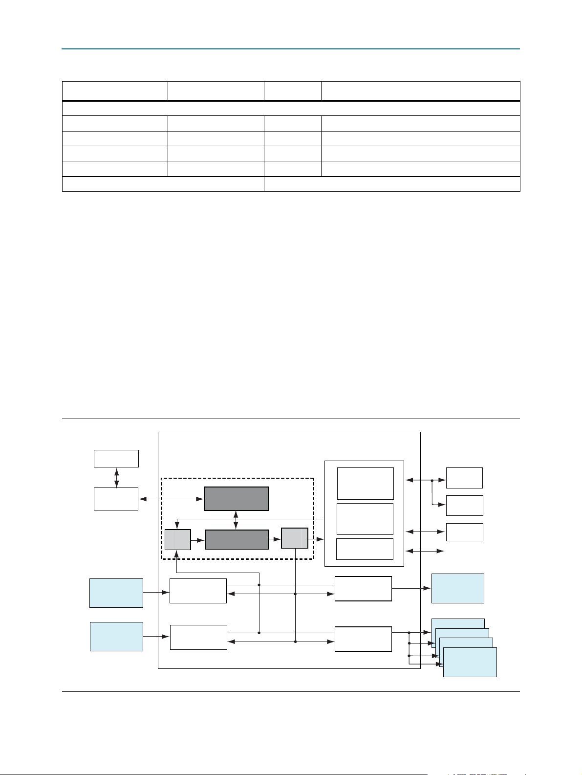
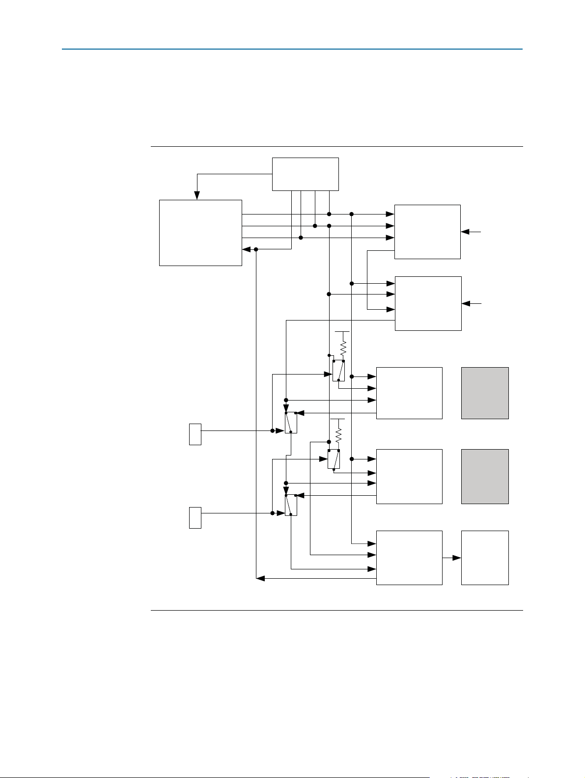
Development Board Block Diagram
Development Board Block Diagram
Figure 1–1 shows the block diagram of the Stratix V Advanced Systems development
board.
Figure 1–1. Stratix V Advanced Systems Development Board Block Diagram
Handling the Board
When handling the board, it is important to observe the following static discharge
precaution:
c Without proper anti-static handling, the board can be damaged. Therefore, use
anti-static handling precautions when touching the board.
January 2014 Altera Corporation Stratix V Advanced Systems Development Board
Reference Manual
Page 10

1–6 Chapter 1: Overview
Handling the Board
Stratix V Advanced Systems Development Board January 2014 Altera Corporation
Reference Manual
Page 11

2. Board Components
This chapter introduces all the important components on the Stratix V Advanced
Systems development board. Figure 2–1 illustrates major component locations and
Tab le 2– 1 provides a brief description of all features of the board.
1 A complete set of schematics, a physical layout database, and ODB++ files for the
development board reside in the Stratix V Advanced Systems development kit
board_design_files directory.
f For information about powering up the board and installing the demo software, refer
to the Stratix V Advanced Systems Development Kit User Guide.
This chapter consists of the following sections:
■ “Board Overview”
■ “Featured Device: Stratix V GX FPGA” on page 2–5
■ “MAX V CPLD System Controller” on page 2–7
■ “Configuration, Status, and Setup Elements” on page 2–12
■ “Clock Circuitry” on page 2–22
■ “General User Input/Output” on page 2–26
■ “Components and Interfaces” on page 2–30
■ “Memory” on page 2–42
■ “Power Supply” on page 2–65
January 2014 Altera Corporation Stratix V Advanced Systems Development Board
Reference Manual
Page 12
2–2 Chapter 2: Board Components
HSMC Port (J1) MoSys (U14)
MoSys (U4)
Powe r
Switch
(SW2)
12V-15 V
DC Input
Jack (J7)
QDRII+ x18
(U5)
QDRII+ x18
(U40)
QDRII+ x18
(U5)
QDRII+ x18
(U22)
DDR3 Memory x16
(U17, U24, U33)
DDR3 Memory x16
(U32, U39, U43)
DDR3 Memory x16
(U36, U21, U27)
DDR3 Memory x16
(U19, U30, U34)
AT X
Header (J9)
JTAG Header
(J11)
SMA Clock Input
Connector (J4, J5)
CPU Reset
Push Button
(S11)
CPU Reset
Push Button
(S7)
PCI Express
Edge Connector
(J13)
Fan Power
Header (J2)
On-Board
USB-Blaster II
Connector (J6)
Program Load,
Program Select
Push Button (S1, S2)
MAX V Reset
Push Button (S3)
Stratix V GX
FPGA (U29)
Stratix V GX
FPGA (U35)
General User
Push Button
(S8, S9, S10)
General User
Push Button
(S4, S5, S6)
User DIP Switch (SW3)
User DIP Switch
(SW1)
FMC (J8)
Board Overview
Board Overview
This section provides an overview of the Stratix V Advanced Systems development
board, including an annotated board image and component descriptions. Figure 2–1
provides an overview of the development board features.
Figure 2–1. Overview of the Stratix V Advanced Systems Development Board Features
Tab le 2– 1 describes the components and lists their corresponding board references.
Table 2–1. Stratix V Advanced Systems Development Board Components (Part 1 of 4)
Board Reference Type Description
Featured Devices
U29, U35 FPGA 5SGXEA7N2F45C2N, 1932-pin BGA.
U73 CPLD 5M2210ZF256C4, 256-pin BGA.
Configuration, Status, and Setup Elements
J11 JTAG header
J6 On-Board USB-Blaster II Mini-USB 2.0 connector for programming and debugging the FPGA.
SW7 JTAG DIP switch
SW5
SW6
FPGA1 mode select DIP
switch
FPGA2 mode select DIP
switch
Provides access to the JTAG chain by using an external USB-Blaster
cable (disables the on-board USB-Blaster II).
Enables and disables devices in the JTAG chain. This switch is located
on the back of the board.
Sets the Stratix V (U29)
the board.
Sets the Stratix V (U35)
the board.
MSEL[2:0]
MSEL[2:0]
pins. FPGA1
pins. FPGA2
MSEL[4:3]
MSEL[4:3]
= 10 on
= 10 on
Controls the MAX V CPLD System Controller functions such as clock
SW4 Board settings DIP switch
select, clock enable, and FPP configuration control. This switch is
located at the bottom of the board.
Stratix V Advanced Systems Development Board January 2014 Altera Corporation
Reference Manual
Page 13
Chapter 2: Board Components 2–3
Board Overview
Table 2–1. Stratix V Advanced Systems Development Board Components (Part 2 of 4)
Board Reference Type Description
SW8 PCI Express DIP switch
Controls the PCI Express lane width by connecting the
together on the PCI Express edge connector. This switch is located at
prsnt
pins
the back of the board.
S1 Program select push button
S2
Program configuration push
button
Toggles the program LEDs, which selects the program image that
loads from flash memory to the FPGAs.
Configures the FPGAs from flash memory image based on the program
LEDs.
Illuminates to show the LED sequence that determines which flash
D1, D2, D3 Program LEDs
memory image loads to the FPGA when you press the program select
push button.
D12 Load LED Illuminates during FPGA configuration.
D13 Configuration done LED Illuminates when the FPGA is configured.
D14 Error LED Illuminates when the FPGA configuration from flash fails.
D27 Power LED Illuminates when 5-V power is present.
Indicate the transmit or receive activity of the System Console USB
D4, D5 System Console TX/RX LEDs
interface. The TX and RX LEDs would flicker if the link is in use and
active. The LEDs are either off when not in use or on when in use but
idle.
Indicate the transmit or receive activity of the JTAG chain. The TX and
D15, D16 JTAG TX/RX LEDs
RX LEDs would flicker if the link is in use and active. The LEDs are
either off when not in use or on when in use but idle.
D10, D11 HSMC TX/RX LEDs
You can configure these LEDs to indicate transmit or receive activity on
the HSMC interface.
D21 HSMC Present LED Illuminates when you plug a daughtercard into the HSMC connector.
D36 FMC Present LED Illuminates when you plug a daughtercard into the FMC connector.
D42, D43 PCI Express Gen2/Gen3 LED
D38, D39, D40,
D41
PCI Express Link LEDs
You can configure these LEDs to illuminate when PCI Express is in
Gen2 or Gen3 mode.
You can configure these LEDs to display the PCI Express link width
(x1, x4, x8, x16).
Clock Circuitry
X1 125 M oscillator
X2 50 M oscillator
U53 Quad-output oscillator
U82 Quad-output oscillator
U95 Quad-output oscillator
U100 Quad-output oscillator
X91 Quad-output oscillator
January 2014 Altera Corporation Stratix V Advanced Systems Development Board
125.000-MHz crystal oscillator for general purpose logic. A buffered
copy of this clock is available on FPGA1 and FPGA2.
50.000-MHz crystal oscillator for general purpose logic. A buffered
copy of this clock is available on FPGA1, FPGA2, and MAX V CPLD.
Programmable oscillator with default LVDS frequencies of 625 MHz,
206.25 MHz, 625 MHz, and 206.25 MHz.
Programmable oscillator with default frequencies of 100 MHz (LVDS),
100 MHz (LVDS), 100 MHz (1.8-V CMOS), and 100 MHz (LVDS).
Programmable oscillator with default LVDS frequencies of 100 MHz,
706.25 MHz, 206.25 MHz, and 206.25 MHz.
Programmable oscillator with default frequencies of 100 MHz (LVDS),
100 MHz (LVDS), 100 MHz (1.8-V CMOS), and 100 MHz (LVDS).
Programmable oscillator with default LVDS frequencies of 100 MHz,
644.53125 MHz, 644.53125 MHz, and 100 MHz.
Reference Manual
Page 14
2–4 Chapter 2: Board Components
Board Overview
Table 2–1. Stratix V Advanced Systems Development Board Components (Part 3 of 4)
Board Reference Type Description
X3 100 M oscillator 100-MHz crystal oscillator for the MAX V CPLD System Controller.
J4, J5 Clock input SMAs Drives LVDS-compatible clock inputs into the clock multiplexer buffer.
General User Input and Output
D6-D9, D17-D20,
D22-D31
D22-D25,
D28-D31
FPGA1 user LEDs
FPGA2 user LEDs
SW1 FPGA1 user DIP switch
SW3 FPGA2 user DIP switch
Two sets of eight bi-color LEDs (green and red) for 16 user LEDs for
FPGA1. Illuminates when driven low.
Two sets of eight bi-color LEDs (green and red) for 16 user LEDs for
FPGA2. Illuminates when driven low.
Octal user DIP switch for FPGA1. When the switch is ON, a logic 0 is
selected.
Octal user DIP switch for FPGA2. When the switch is ON, a logic 0 is
selected.
S3 MAX V reset push button The default reset for the MAX V CPLD System Controller.
S7 FPGA1 CPU reset push button The default reset for the FPGA1 logic.
S11 FPGA2 CPU reset push button The default reset for the FPGA2 logic.
S4-S6
S8-S10
FPGA1 general user push
button
FPGA2 general user push
button
Three user push buttons for FPGA1. Driven low when pressed.
Three user push buttons for FPGA2. Driven low when pressed.
Memory Devices
U19, U57 DDR3A x32
U30, U34, U72,
U80
DDR3B x64
U36, U81 DDR3C x32
U21, U27, U58,
U68
DDR3D x64
U32, U75, DDR3E x32
U39, U43, U88,
U92
DDR3F x64
U33, U78 DDR3G x32
U17, U24, U55,
U64
U12, U52, U41,
U90
U22, U61, U40,
U89
DDR3H x64
QDRII+ x18 (interfaces A to D)
QDRII+ x18 (interfaces E to H)
U4 MoSys x16
512-MB DDR3 x64-bit data bus interfacing to FPGA1, consisting of
two x16-bit devices with a single address and command bus.
1024-MB DDR3 x64-bit data bus interfacing to FPGA1, consisting of
four x16-bit devices with a single address and command bus.
512-MB DDR3 x64-bit data bus interfacing to FPGA1, consisting of
two x16-bit devices with a single address and command bus.
1024-MB DDR3 x64-bit data bus interfacing to FPGA1, consisting of
four x16-bit devices with a single address and command bus.
512-MB DDR3 x64-bit data bus interfacing to FPGA2, consisting of
two x16-bit devices with a single address and command bus.
1024-MB DDR3 x64-bit data bus interfacing to FPGA2, consisting of
four x16-bit devices with a single address and command bus.
512-MB DDR3 x64-bit data bus interfacing to FPGA2, consisting of
two x16-bit devices with a single address and command bus.
1024-MB DDR3 x64-bit data bus interfacing to FPGA2, consisting of
four x16-bit devices with a single address and command bus.
Four 4.5-MB QDRII+ SRAM interfaces with a 18-bit data bus for
FPGA1. The device has a separate 18-bit read and 18-bit write port with
DDR signalling at up to 533 MHz.
Four 4.5-MB QDRII+ SRAM interfaces with a 18-bit data bus for
FPGA2. The device has a separate 18-bit read and 18-bit write port with
DDR signalling at up to 533 MHz.
A 72-MB MoSys Bandwidth Engine IC SRAM with a 16-bit transceiver
data bus for FPGA1.
Stratix V Advanced Systems Development Board January 2014 Altera Corporation
Reference Manual
Page 15
Chapter 2: Board Components 2–5
Featured Device: Stratix V GX FPGA
Table 2–1. Stratix V Advanced Systems Development Board Components (Part 4 of 4)
Board Reference Type Description
U14 MoSys x16
U86 Flash x16
U93, U48 EPCQ x4
U76, U83 EEPROM
Communication Ports
J13 PCI Express edge connector
U47 PLX PCI Express switch
J8 FMC port Provides 10 transceiver channels and 74 CMOS or 17 LVDS channels.
J1 HSMC port
A 72-MB MoSys Bandwidth Engine IC SRAM with a 16-bit transceiver
data bus for FPGA2.
A 1-Gb synchronous flash device with a 16-bit data bus for non-volatile
memory. Only accessible from the MAX V System Controller, intended
for FPGA configuration.
A 32-MB serial flash is available for each FPGA to use during active
serial (AS) configuration.
A single 8-Kbit serial EEPROM is available for each FPGA to store
board information.
Made of gold-plated edge fingers for up to ×16 signaling in either
Gen1, Gen2, or Gen3 mode.
Switch x16 PCI Express data between FPGA1 x8 and FPGA2 x8 via the
PEX8747 PCIe switch.
Provides eight transceiver channels and 84 CMOS or 17 LVDS
channels.
Power Supply
J13 PCI Express edge connector
J10 PCI Express 2x4 ATX power
J7 DC input jack Accepts a 12- to 15-V DC power supply.
SW2 Power switch
Interfaces to a PCI Express root port such as an appropriate PC
motherboard.
PCI Express compliant 2x4 auxiliary power connector. This can supply
an additional 150 W to the board.
Switch to power on or off the board when power is supplied from the
DC input jack.
Featured Device: Stratix V GX FPGA
The Stratix V Advanced Systems development board features two Stratix V GX FPGA
5SGXEA7N2F45C2N devices (U29, U35) in a 1932-pin FineLine BGA package.
f For more information about the Stratix V device family, refer to the Stratix V Device
Handbook.
Tab le 2– 2 describes the features of the Stratix V GX FPGA 5SGXEA7N2F45C2N
device.
Table 2–2. Stratix V GX FPGA 5SGXEA7N2F45C2N Features
ALMs
358,500 622,000 939,000 50 512 28 48
Equivalent
LEs
Registers
M20K
Memory (Mb)
18-bit × 18-bit
Multipliers
Fractional
PLLs
Transceiver Channels
(12.5 Gbps)
Package Type
1932-pin
FineLine BGA
January 2014 Altera Corporation Stratix V Advanced Systems Development Board
Reference Manual
Page 16
2–6 Chapter 2: Board Components
Featured Device: Stratix V GX FPGA
I/O Resources
Tab le 2– 3 lists the Stratix V GX FPGA device pin count and usage by function on the
development board.
Table 2–3. Stratix V GX FPGA Pin Count and Usage (Part 1 of 2)
Function I/O Standard I/O Count Special Pins
FPGA1
DDR3 1.5-V SSTL 368 4 differential, 24 differential DQS
QDRII+ 1.5-V SSTL 260 4 differential DQS
EEPROM 2.5-V CMOS 2
FMC Adjustable 80 36 differential, 2 reference clocks
Switches 1.5-V CMOS 8
LEDs 1.5-V/2.5-V CMOS 19
Push buttons 1.5-V/2.5-V CMOS 4
Chip-to-chip 2.5-V CMOS + LVDS 20 4 differential
MAX V Interface 1.5-V/2.5-V CMOS 4
MoSys 1.5-V CMOS 10
PCI Express/PLX 1.5-V/2.5-V CMOS 10
Clocks or Oscillators 1.5-V CMOS + LVDS 26 5 differential clock, 7 differential reference clocks
On-board USB-Blaster II 1.5-V CMOS 19
Total I/O Used: 830
Transceiver Pairs
Chip-to-chip 8
FMC 10
MoSys 16
PCI Express/PLX 8
Total Transceivers Used: 42
FPGA2
DDR3 1.5-V SSTL 368 4 differential, 24 differential DQS
QDRII+ 1.5-V SSTL 260 4 differential DQS
EEPROM 2.5-V CMOS 2
HSMC 2.5-V CMOS + LVDS 84 38 differential, 3 clocks
Switches 1.5-V CMOS 8
LEDs 1.5-V CMOS 19
Push-buttons 1.5-V/2.5-V CMOS 4
Chip-to-chip 2.5-V CMOS + LVDS 20 4 differential
MAX V Interface 1.5-V/2.5-V CMOS 4
MoSys 1.5-V CMOS 10
PCI Express/PLX 1.5-V/2.5-V CMOS 6
Clocks or Oscillators 1.5-V CMOS + LVDS 24 5 differential clock, 6 differential reference clocks
Total I/O Used: 809
Stratix V Advanced Systems Development Board January 2014 Altera Corporation
Reference Manual
Page 17
Chapter 2: Board Components 2–7
Information
Register
On-Board
USB-Blaster II
Si5538
Controller
Si570
Controller
SLD-HUB
PFL
MAX V System Controller
Power
Measurement
Results
Virtual-JTAG
PC
Temperature
Measurement
Results
FPGA1
LTC2418
Controller
MAX1619
Controller
FPGA2
Decoder
Encoder
GPIO
JTAG Control
Flash
Control
Register
Si570
Programmable
Oscillator
Si5338
Programmable
Oscillator
Si5338
Programmable
Oscillator
Si5338
Programmable
Oscillator
Si5338
Programmable
Oscillator
MAX V CPLD System Controller
Table 2–3. Stratix V GX FPGA Pin Count and Usage (Part 2 of 2)
Function I/O Standard I/O Count Special Pins
Transceiver Pairs
Chip-to-chip 8
HSMC 8
MoSys 16
PCI Express/PLX 8
Total Transceivers Used: 40
MAX V CPLD System Controller
The board utilizes the 5M2210ZF256C4 System Controller, an Altera MAX V CPLD,
for the following purposes:
■ FPGA configuration from flash memory
■ Power consumption monitoring
■ Temp e ra tu re m onito ri ng
■ Fan control
■ Control registers for clocks
■ Control registers for remote system update
Figure 2–2 illustrates the MAX V CPLD System Controller's functionality and external
circuit connections as a block diagram.
Figure 2–2. MAX V CPLD System Controller Block Diagram
January 2014 Altera Corporation Stratix V Advanced Systems Development Board
Reference Manual
Page 18
2–8 Chapter 2: Board Components
MAX V CPLD System Controller
Tab le 2– 4 lists the I/O signals present on the MAX V CPLD System Controller. The
signal names and functions are relative to the MAX V device (U73).
Table 2–4. MAX V CPLD System Controller Device Pin-Out (Part 1 of 5)
Schematic Signal Name
CLK125_EN
CLK50_EN
CLK_CONFIG
CLK_ENABLE
CLK_SEL
CLOCK_SCL
CLOCK_SDA
FACTORY_LOAD
FACTORY_REQUEST
FACTORY_STATUS
FLASH_ADVN
FLASH_CEN
FLASH_CLK
FLASH_OEN
FLASH_RDYBSYN
FLASH_RESETN
FLASH_WEN
FLASH_WPN
FLASH_A1
FLASH_A2
FLASH_A3
FLASH_A4
FLASH_A5
FLASH_A6
FLASH_A7
FLASH_A8
FLASH_A9
FLASH_A10
FLASH_A11
FLASH_A12
FLASH_A13
FLASH_A14
FLASH_A15
FLASH_A16
FLASH_A17
FLASH_A18
MAX V CPLD
Pin Number
I/O
Standard
Description
A2 2.5-V 125 MHz oscillator enable
E9 2.5-V 50 MHz oscillator enable
J5 2.5-V 100 MHz configuration clock input
C13 2.5-V DIP switch for clock oscillator enable
D11 2.5-V DIP switch for clock select SMA or oscillator
M2 2.5-V Programmable oscillator I2C clock
M3 2.5-V Programmable oscillator I2C data
B13 2.5-V DIP switch to load factory image from flash at power-up
R14 1.5-V On-Board USB-Blaster II request to send factory command
N12 1.5-V On-Board USB-Blaster II factory command status
K12 1.8-V FM bus flash memory address valid
D13 1.8-V FM bus flash memory chip enable
F12 1.8-V FM bus flash memory clock
D14 1.8-V FM bus flash memory output enable
F11 1.8-V FM bus flash memory chip ready 0
P14 1.8-V FM bus flash memory reset
K13 1.8-V FM bus flash memory write enable
M14 1.8-V FM bus flash memory write protect
C14 1.8-V FM address bus
C15 1.8-V FM address bus
E13 1.8-V FM address bus
E12 1.8-V FM address bus
D15 1.8-V FM address bus
F14 1.8-V FM address bus
D16 1.8-V FM address bus
F13 1.8-V FM address bus
E15 1.8-V FM address bus
E16 1.8-V FM address bus
F15 1.8-V FM address bus
G14 1.8-V FM address bus
F16 1.8-V FM address bus
G13 1.8-V FM address bus
N16 1.8-V FM address bus
G12 1.8-V FM address bus
G16 1.8-V FM address bus
H14 1.8-V FM address bus
Stratix V Advanced Systems Development Board January 2014 Altera Corporation
Reference Manual
Page 19

Chapter 2: Board Components 2–9
MAX V CPLD System Controller
Table 2–4. MAX V CPLD System Controller Device Pin-Out (Part 2 of 5)
Schematic Signal Name
FLASH_A19
FLASH_A20
FLASH_A21
FLASH_A22
FLASH_A23
FLASH_A24
FLASH_A25
FLASH_A26
FLASH_D0
FLASH_D1
FLASH_D2
FLASH_D3
FLASH_D4
FLASH_D5
FLASH_D6
FLASH_D7
FLASH_D8
FLASH_D9
FLASH_D10
FLASH_D11
FLASH_D12
FLASH_D13
FLASH_D14
FLASH_D15
FMC_C2M_PG
FPGA1_CONF_DONE
FPGA1_CPU_RESETN
FPGA1_CVP_CONFDONE
FPGA1_DCLK
FPGA1_FPP
FPGA1_MSEL0
FPGA1_MSEL1
FPGA1_MSEL2
FPGA1_MSEL3
FPGA1_MSEL4
FPGA1_NCE
FPGA1_NCEO
FPGA1_NCONFIG
FPGA1_NSTATUS
MAX V CPLD
Pin Number
I/O
Standard
Description
H15 1.8-V FM address bus
H13 1.8-V FM address bus
H16 1.8-V FM address bus
J13 1.8-V FM address bus
J16 1.8-V FM address bus
G15 1.8-V FM address bus
L16 1.8-V FM address bus
E14 1.8-V FM address bus
J14 1.8-V FM data bus
J15 1.8-V FM data bus
K16 1.8-V FM data bus
N15 1.8-V FM data bus
K15 1.8-V FM data bus
N14 1.8-V FM data bus
L14 1.8-V FM data bus
L11 1.8-V FM data bus
L15 1.8-V FM data bus
L12 1.8-V FM data bus
M16 1.8-V FM data bus
L13 1.8-V FM data bus
M15 1.8-V FM data bus
M13 1.8-V FM data bus
K14 1.8-V FM data bus
P15 1.8-V FM data bus
E3 2.5-V FMC carrier card to mezzanine module power good
A13 2.5-V FPGA1 configuration done
B1 2.5-V FPGA1 reset
N10 1.5-V FPGA1 configuration via protocol done
J3 2.5-V FPGA1 configuration clock
A15 2.5-V Configure FPGA1 via FPP at power up
A7 2.5-V DIP switch for FPGA1 mode select 0
E1 2.5-V DIP switch for FPGA1 mode select 1
A6 2.5-V DIP switch for FPGA1 mode select 2
A12 2.5-V FPGA1 mode select 3
A5 2.5-V FPGA1 mode select 4
B3 2.5-V FPGA1 chip enable
F1 2.5-V FPGA1 chip enable output
K2 2.5-V FPGA1 configuration active
J4 2.5-V FPGA1 configuration ready status
January 2014 Altera Corporation Stratix V Advanced Systems Development Board
Reference Manual
Page 20
2–10 Chapter 2: Board Components
MAX V CPLD System Controller
Table 2–4. MAX V CPLD System Controller Device Pin-Out (Part 3 of 5)
Schematic Signal Name
FPGA1_OVERTEMP
FPGA1_OVERTEMPN
FPGA1_PR_DONE
FPGA1_PR_ERROR
FPGA1_PR_READY
FPGA1_PR_REQUEST
FPGA2_CONF_DONE
FPGA2_CPU_RESETN
FPGA2_CVP_CONFDONE
FPGA2_DCLK
FPGA2_FPP
FPGA2_MSEL0
FPGA2_MSEL1
FPGA2_MSEL2
FPGA2_MSEL3
FPGA2_MSEL4
FPGA2_NCE
FPGA2_NCEO
FPGA2_NCONFIG
FPGA2_NSTATUS
FPGA2_OVERTEMP
FPGA2_OVERTEMPN
FPGA2_PR_DONE
FPGA2_PR_ERROR
FPGA2_PR_READY
FPGA2_PR_REQUEST
FPGA_CONFIG_D0
FPGA_CONFIG_D1
FPGA_CONFIG_D2
FPGA_CONFIG_D3
FPGA_CONFIG_D4
FPGA_CONFIG_D5
FPGA_CONFIG_D6
FPGA_CONFIG_D7
HSMC_PRSNTN
JTAG_5M2210_TDI
JTAG_5M2210_TDO
JTAG_TCK
JTAG_TMS
MAX V CPLD
Pin Number
I/O
Standard
Description
A11 2.5-V FPGA1 temperature monitor fan enable
D7 2.5-V FPGA1 temperature monitor over-temperature indicator LED
N9 1.5-V FPGA1 partial reconfiguration done
M10 1.5-V FPGA1 partial reconfiguration error
M8 1.5-V FPGA1 partial reconfiguration ready
R3 1.5-V FPGA1 partial reconfiguration request
P2 2.5-V FPGA2 configuration done
N3 2.5-V FPGA2 reset
T2 2.5-V FPGA2 configuration via protocol done
K5 2.5-V FPGA2 configuration clock
B14 2.5-V Configure FPGA2 via FPP at power up
G1 2.5-V DIP switch for FPGA2 mode select 0
L1 2.5-V DIP switch for FPGA2 mode select 1
J1 2.5-V DIP switch for FPGA2 mode select 2
N1 2.5-V FPGA2 mode select 3
M1 2.5-V FPGA2 mode select 4
K1 2.5-V FPGA2 chip enable
M4 2.5-V FPGA2 chip enable output
L5 2.5-V FPGA2 configuration active
H1 2.5-V FPGA2 configuration ready status
D10 2.5-V FPGA2 temperature monitor fan enable
E10 2.5-V FPGA2 temperature monitor over-temperature indicator LED
R6 1.5-V FPGA2 partial reconfiguration done
R1 1.5-V FPGA2 partial reconfiguration error
T5 1.5-V FPGA2 partial reconfiguration ready
R5 1.5-V FPGA2 partial reconfiguration request
D3 2.5-V FPGA configuration data
C2 2.5-V FPGA configuration data
C3 2.5-V FPGA configuration data
D1 2.5-V FPGA configuration data
D2 2.5-V FPGA configuration data
E4 2.5-V FPGA configuration data
D4 2.5-V FPGA configuration data
E5 2.5-V FPGA configuration data
B8 2.5-V HSMC port present
L6 2.5-V MAX V JTAG data in
M5 2.5-V MAX V JTAG data out
P3 2.5-V MAX V JTAG clock
N4 2.5-V MAX V JTAG TMS
Stratix V Advanced Systems Development Board January 2014 Altera Corporation
Reference Manual
Page 21
Chapter 2: Board Components 2–11
MAX V CPLD System Controller
Table 2–4. MAX V CPLD System Controller Device Pin-Out (Part 4 of 5)
Schematic Signal Name
M570_CLOCK
M570_PCIE_JTAG_EN
MAX5_CLK
MAX5_DATA
MAX_CONF_DONE
MAX_ERROR
MAX_LOAD
MAX_RESETN
MV_CLK_50
PGM_CONFIG
PGM_LED0
PGM_LED1
PGM_LED2
PGM_SEL
SENSE_CS0N
SENSE_SCK
SENSE_SDI
SENSE_SDO
SENSE_SMB_CLK
SENSE_SMB_DATA
SI53154_SCLK
SI53154_SDATA
TSENSE_ALERTN_1
TSENSE_ALERTN_2
USB_CFG0
USB_CFG1
USB_CFG2
USB_CFG3
USB_CFG4
USB_CFG5
USB_CFG6
USB_CFG7
USB_CFG8
USB_CFG9
USB_CFG10
USB_CFG11
USB_CFG12
USB_CFG13
MAX V CPLD
Pin Number
I/O
Standard
Description
P11 1.5-V 25-MHz clock to on-board USB-Blaster II
E11 2.5-V Reserved
T11 1.5-V MAX V clock
P5 1.5-V MAX V data
C11 2.5-V FPGA configuration done LED
A9 2.5-V FPGA configuration error LED
B12 2.5-V FPGA configuration active LED
M9 1.5-V MAX V reset push button
J12 1.8-V 50-MHz clock input
D9 2.5-V Loads the flash memory image identified by the PGM LEDs
B9 2.5-V Flash memory PGM select indicator 0
C10 2.5-V Flash memory PGM select indicator 1
D12 2.5-V Flash memory PGM select indicator 2
C9 2.5-V Toggles the
PGM_LED[0:2]
sequence
C12 2.5-V Power monitor chip select
B6 2.5-V Power monitor SPI clock
B11 2.5-V Power monitor SPI data in
B10 2.5-V Power monitor SPI data out
E7 2.5-V Temperature monitor SMB clock
E6 2.5-V Temperature monitor SMB data
C8 2.5-V Si53154 serial clock
A10 2.5-V Si53154 serial data
D8 2.5-V FPGA1 temperature monitor alert
B5 2.5-V FPGA2 temperature monitor alert
P8 1.5-V On-board USB Blaster II configuration
N6 1.5-V On-board USB Blaster II configuration
M6 1.5-V On-board USB Blaster II configuration
M7 1.5-V On-board USB Blaster II configuration
N8 1.5-V On-board USB Blaster II configuration
N7 1.5-V On-board USB Blaster II configuration
P9 1.5-V On-board USB Blaster II configuration
N11 1.5-V On-board USB Blaster II configuration
T9 1.5-V On-board USB Blaster II configuration
T10 1.5-V On-board USB Blaster II configuration
R9 1.5-V On-board USB Blaster II configuration
T8 1.5-V On-board USB Blaster II configuration
R16 1.5-V On-board USB Blaster II configuration
T13 1.5-V On-board USB Blaster II configuration
January 2014 Altera Corporation Stratix V Advanced Systems Development Board
Reference Manual
Page 22

2–12 Chapter 2: Board Components
Configuration, Status, and Setup Elements
Table 2–4. MAX V CPLD System Controller Device Pin-Out (Part 5 of 5)
Schematic Signal Name
USB_CFG14
USB_CLK
MAX V CPLD
Pin Number
T15 1.5-V On-board USB Blaster II configuration
H5 2.5-V On-board USB Blaster II clock
I/O
Standard
Configuration, Status, and Setup Elements
This section describes the board's configuration, status, and setup elements.
Configuration
This section describes the FPGA, flash memory, and MAX V CPLD System Controller
device programming methods that the Stratix V Advanced Systems development
board supports.
The Stratix V Advanced Systems development board supports three configuration
methods:
■ On-Board USB-Blaster II is the default method for configuring the FPGA using the
Quartus II Programmer in JTAG mode with the supplied mini-USB cable.
■ Parallel flash memory download for configuring the FPGAs using stored images
from the flash memory via FPP at either board power-up or by pressing the
program configuration push button (S2).
Description
■ Serial flash memory download for configuring either FPGA at board power-up via
active serial (x4 AS).
■ External USB-Blaster for configuring the FPGA using an external USB-Blaster.
FPGA Programming over On-Board USB-Blaster II
The on-board USB-Blaster II is implemented using a mini-USB type-B connector (J6), a
USB 2.0 PHY device, and an Altera MAX II CPLD EPM570F100 (U77). This allows for
FPGA configuration using a USB cable that connects directly between the USB port on
the board and a USB port on a PC running the Quartus II software. The on-board
USB-Blaster II masters the JTAG chain.
f For more information about the on-board USB-Blaster II, refer to the on-board
USB-Blaster II page of the Altera Wiki website.
Stratix V Advanced Systems Development Board January 2014 Altera Corporation
Reference Manual
Page 23
Chapter 2: Board Components 2–13
Configuration, Status, and Setup Elements
MAX II CPLD EPM570F100
The MAX II CPLD is dedicated to the on-board USB-Blaster II function. The CPLD
connects to the USB 2.0 PHY device on one side and drives the JTAG signals out the
other side through the general purpose I/O (GPIO) pins.
Tab le 2– 5 lists the I/O signals present on the MAX II CPLD EPM570F100.
Table 2–5. MAX II CPLD On-Board USB-Blaster II I/O Signals
Schematic Signal Name Type Description
SC_RX
SC_TX
JTAG_RX
JTAG_TX
C_JTAG_TCK
C_JTAG_TMS
C_JTAG_TDI
C_JTAG_TDO
USB_CFG(14:0)
USB_CLK
USB_OEn
USB_RESETn
USB_DATA(7:0)
USB_RDn
USB_WRn
USB_EMPTY
USB_FULL
USB_ADDR(1:0)
USB_SCL
USB_SDA
FACTORY_REQUEST
FACTORY_STATUS
M570_CLOCK
1.5-V CMOS output USB system console receive LED
1.5-V CMOS output USB system console transmit LED
1.5-V CMOS output USB-Blaster II JTAG receive LED
1.5-V CMOS output USB-Blaster II JTAG transmit LED
2.5-V CMOS output GPIO for on-board JTAG chain clock
2.5-V CMOS output GPIO for on-board JTAG chain mode
2.5-V CMOS output GPIO for on-board JTAG chain data in
2.5-V CMOS input GPIO for on-board JTAG chain data out
1.5-V CMOS input/output
Configuration data between the MAX V System
Controller and the on-board USB-Blaster II.
2.5-V CMOS input USB System Console clock
1.5-V CMOS input USB System Console FPGA output enable
1.5-V CMOS input USB System Console reset
1.5-V CMOS inout (8 bits) USB System Console FIFO data bus
1.5-V CMOS input USB System Console read from FIFO
1.5-V CMOS input USB System Console write to FIFO
1.5-V CMOS output USB System Console FIFO empty
1.5-V CMOS output USB System Console FIFO full
1.5-V CMOS input/output USB System Console address bus
1.5-V CMOS input/output USB System Console configuration clock
1.5-V CMOS input/output USB System Console configuration data
1.5-V CMOS input Send FACTORY command
1.5-V CMOS output FACTORY command status
1.5-V CMOS input 25-MHz input clock for FACTORY command
January 2014 Altera Corporation Stratix V Advanced Systems Development Board
Reference Manual
Page 24
2–14 Chapter 2: Board Components
GPIO
Cypress
On-Board
USB-Blaster II
Analog
Switch
5M2210
System
Controller
FMC
HSMC
GPIO
GPIO
GPIO
JTAG Master
GPIO
DISABLE
JTAG Slave
JTAG Slave
Installed
HSMC
Card
Installed
FMC
Card
Flash
Memory
TCK
TMS
TDI
TDO
TCK
TMS
TDI
TDO
TCK
TMS
TDI
TDO
TCK
TMS
TDI
TDO
JTAG Slave
JTAG Slave
5SGXA7
FPGA1
5SGXA7
FPGA2
Analog
Switch
ENABLE
ENABLE
ALWAYS
ENABLED
(in chain)
ALWAYS
ENABLED
(in chain)
DIP Switch
DIP Switch
10-pin
JTAG Header
TCK
TMS
TDI
TDO
JTAG Slave
TCK
TMS
TDO
TDI
2.5 V
2.5 V
Configuration, Status, and Setup Elements
JTAG Chain
The on-board USB-Blaster II is automatically disabled when you connect an external
USB-Blaster to the JTAG chain or when you enable JTAG from the PCI Express edge
connector. Figure 2–3 illustrates the JTAG chain.
Figure 2–3. JTAG Chain
Each jumper shown in Figure 2–3 is located in the JTAG DIP switch (SW7) on the back
of the board. Both the Stratix V FPGAs and the MAX VSystem Controller are always
in the JTAG chain. To connect the HSMC or FMC interface in the chain, their
corresponding switch must be in the OFF position.
Stratix V Advanced Systems Development Board January 2014 Altera Corporation
Reference Manual
Page 25
Chapter 2: Board Components 2–15
Configuration, Status, and Setup Elements
1 By default, the on-board USB-Blaster II clocks
TCK
at 24 MHz. For the on-board
USB-Blaster II to function correctly, you must set the Quartus II clock constraint on the
altera_reserved_tck
input signal to 24 MHz.
System Console USB Interface
The System Console USB interface is a fast parallel interface available on FPGA1.
Together with the soft logic supplied by Altera, this interface provides a System
Console master for debug access.
The System Console controls the debug master via signals shown in Tab le 2 –6 to give
fast access to an Avalon
®
Memory-Mapped (Avalon-MM) master bus that the Qsys
system integration tool generates.
f For more information about the System Console, refer to the Analyzing and Debugging
Designs with the System Console chapter in volume 3 of the Quartus II Handbook.
Tab le 2 –6 lists the System Console USB interface pin connections relative to the FPGA.
Table 2–6. System Console USB Interface Pin Connections
Stratix V GX FPGA1 (U29) Pin Number Schematic Signal Name Direction Note
BC8
BD34
BA15, AJ13, AR16, AH13, BD14, AF17,
BC14, AP13
AW33
AU35
AJ29
AT33
AV34
AF13, BD10
BD35
BA31
usb_clk
usb_resetn
usb_data[7:0]
usb_full
usb_empty
usb_wrn
usb_rdn
usb_oen
usb_addr[1:0]
usb_scl
usb_sda
input 48 MHz
input —
bidirectional BA15 (MSB), AP13 (LSB)
output —
output —
input —
input —
input —
bidirectional Reserved
bidirectional —
bidirectional —
CFI Flash Programming
Flash programming is possible using the pre-built PFL design included in the
development kit to write configuration data to the CFI flash. The development board
implements the Altera PFL megafunction for flash programming. The PFL
megafunction is a block of logic that is programmed into an Altera programmable
logic device, in this case, the MAX V CPLD. The PFL functions as a utility for writing
to a compatible flash device.
This pre-built design contains the PFL megafunction that allows you to write either
page 0, page 1, or other areas of flash over the on-board USB-Blaster II interface using
the Quartus II software.
1 Use this method to restore the development board to its factory default settings.
January 2014 Altera Corporation Stratix V Advanced Systems Development Board
Reference Manual
Page 26
2–16 Chapter 2: Board Components
Configuration, Status, and Setup Elements
FPGA Programming from CFI Flash Memory
On either board power-up or by pressing the program load push button (S2), the
MAX V CPLD System Controller’s parallel flash loader configures the FPGA from the
flash memory. The system controller uses the Altera Parallel Flash Loader (PFL)
megafunction which reads 16-bit data from the flash memory and converts it to fast
passive parallel (FPP) format. This 16-bit data is then written to the FPGA’s dedicated
configuration pins during configuration.
After a board power-up or reset event, the MAX V CPLD (U73) automatically
configures the FPGAs in FPP mode with the pre-installed factory .pof file. There are
three pages reserved for the FPGA configuration data—factory FPGA1 (page 0),
factory FPGA2 (page 1), and user design FPGA1 (page 2).
1 You must set the FPGA1_MSEL[4:0] or FPGA2_MSEL[4:0] DIP switch to FPP x8 mode
to configure FPGA1 or FPGA2 via FPP.
f For more information about the FPP configuration mode, refer to the Configuration,
Design Security, and Remote System Upgrades in Stratix V Devices chapter in the Stratix V
Handbook.
Three green configuration status LEDs,
PGM_LED[2:0]
(D1, D2, D3) indicates the status
of the FPP configuration. Ta bl e 2– 7 lists the configuration status LEDs settings.
Table 2–7. Configuration LED settings
LED
PGM_LED0 PGM_LED1 PGM_LED2
v — — Factory FPGA1
— v —Factory FPGA2
——v User design FPGA1
Note to Tab le 2–7 :
(1) A checkmark (v) indicates that the LED is ON (logic 0) while a dash (—) indicates that the LED is OFF (logic 1).
(1)
Design
Stratix V Advanced Systems Development Board January 2014 Altera Corporation
Reference Manual
Page 27

Chapter 2: Board Components 2–17
MAX V CPLD
System Controller
FPGA_DATA [7:0]
FPGA1_DCLK
FLASH_A [25:1]
FLASH_D [31:0]
FPP Port
DATA [7:0]
DCLK
INIT_DONE
nSTATUS
nCONFIG
CONF_DONE
MSEL0
MSEL1
MSEL2
MSEL3
2.5 V
10 kΩ
nCE
FPGA1
FPGA2
CFI Flash
1 kΩ
FLASH_CEn
FLASH_OEn
FLASH_WEn
FLASH_A [25:0]
FLASH_D [15:0]
FLASH_CEn
FLASH_OEn
FLASH_WEn
FLASH_WPn
FLASH_ADVn
FLASH_ADVn
FPGA1_nCONFIG
FPGA1_CONF_DONE
FLASH_RYBSYn
FPGA1_nSTATUS
FPGA1_nCE
ERROR
LOAD
FACTORY
1.8 V
10 kΩ
2.5 V
FLASH_RYBSYn
PGM_SEL
10 kΩ
FLASH_CLK
FLASH_CLK
FLASH_RSTn
FLASH_RESETn
50 MHz
100 MHz
PGM_CONFIG
MAX_RESETn
2.5 V
1 kΩ
1 kΩ
1 kΩ
MSEL4
MSEL[4:0] also
connects to MAX V
FPGA1_INIT_DONE
FPGA2_DCLK
FPGA2_nCONFIG
FPGA2_CONF_DONE
FPGA2_nSTATUS
FPGA2_nCE
FPGA2_INIT_DONE
2.5 V
56.2 Ω
CLK_SEL
CLK_ENABLE
USER_PGM
USB_SELECT
DIP Switch
DIP Switch
FPP Port
DATA [7:0]
DCLK
INIT_DONE
nSTATUS
nCONFIG
CONF_DONE
MSEL0
MSEL1
MSEL2
MSEL3
2.5 V
10 kΩ
nCE
2.5 V
1 kΩ
1 kΩ
MSEL4
MSEL[4:0] also
connects to MAX V
DIP Switch
PGM_LED0
PGM_LED1
PGM_LED2
2.5 V
56.2 Ω
10 kΩ
Configuration, Status, and Setup Elements
Figure 2–4 shows the PFL configuration.
Figure 2–4. PFL Configuration
January 2014 Altera Corporation Stratix V Advanced Systems Development Board
f For more information on the flash memory map storage, refer to the Stratix V
Advanced Systems Development Kit User Guide.
FPGA Programming from Serial Flash Memory
Each FPGA has an EPCQ (serial flash memory) that connects to it’s Active Serial (AS)
configuration pins. On board power-up, each FPGA can be configured via AS x4
mode from the EPCQ device. The contents of the EPCQ devices are written using the
Altera Serial Flash Loader through the Stratix V GX FPGAdevice.
1 To write to the EPCQ device or configure the FPGA via AS x4 mode, the respective
FPGA must have it’s MSEL[4:0] pins set to AS x4 mode.
Reference Manual
Page 28

2–18 Chapter 2: Board Components
Configuration, Status, and Setup Elements
f For more information about the AS configuration mode, refer to the Configuration,
Design Security, and Remote System Upgrades in Stratix V Devices chapter in the Stratix V
Handbook.
FPGA Programming over External USB-Blaster
The JTAG programming header provides another method for configuring the FPGA
using an external USB-Blaster device with the Quartus II Programmer running on a
PC. The external USB-Blaster connects to the board through the JTAG header (J11).
When you install the external USB-Blaster into the JTAG header, the on-board
USB-Blaster II device is automatically disabled to prevent contention between these
two JTAG masters.
f For more information on the following topics, refer to the respective documents:
■ SFL megafunction, refer to AN 370: Using the Serial Flash Loader with the Quartus II
Software.
■ PFL megafunction, refer to AN 386: Using the Parallel Flash Loader with the
Quartus II Software.
Status Elements
The development board includes board-specific status LEDs and switches for
enabling and configuring various features on the board. This section describes these
status elements.
Status LEDs
Surface mount LEDs indicate various status of the board. A logic 0 is driven on the
I/O port to turn on the LED while a logic 1 is driven to turn off the LED.
Tab le 2 –8 lists the LED board references, names, and functional descriptions.
Table 2–8. Board-Specific LEDs (Part 1 of 2)
Board
Reference
D27 PWR — Blue LED. Illuminates when 5.0-V power is active.
D14 ERROR
D12 LOAD
D13 CONF_DONE
D34 FMC_RX
D35 FMC_TX
D36 FMC_PRSNTn
LED Name
Schematic Signal
Name
MAX_ERROR
MAX_LOAD
MAX_CONF_DONEn
FMC_RX_LED
FMC_TX_LED
FMC_PRSNTn
Description
Red LED. Illuminates when the MAX V CPLD System Controller
fails to configure the FPGA. Driven by the MAX V CPLD System
Controller.
Green LED. Illuminates when the MAX V CPLD System Controller
is actively configuring the FPGA. Driven by the MAX V CPLD
System Controller.
Green LED. Illuminates when the FPGA is successfully
configured. Driven by the MAX V CPLD System Controller.
Green LED. Blinks to indicate FMC receive activity. Driven by
FPGA1.
Green LED. Blinks to indicate FMC transmit activity. Driven by
FPGA1.
Green LED. Illuminates when the FMC is installed. Driven by the
FMC.
Stratix V Advanced Systems Development Board January 2014 Altera Corporation
Reference Manual
Page 29

Chapter 2: Board Components 2–19
Configuration, Status, and Setup Elements
Table 2–8. Board-Specific LEDs (Part 2 of 2)
Board
Reference
LED Name
D10 RX
D11 TX
D21 PRSNTn
D1, D2, D3 PGM_LED[2:0]
D26
D37
OVERTEMP
FPGA1
OVERTEMP
FPGA2
Setup Elements
The development board includes several different kinds of setup elements. This
section describes the following setup elements:
Schematic Signal
Name
HSMC_RX_LED
HSMC_TX_LED
HSMC_PRSNTn
PGM_LED0
PGM_LED1
PGM_LED2
FPGA1_OVERTEMPn
FPGA2_OVERTEMPn
Description
Green LED. Blinks to indicate HSMC receive activity. Driven by
FPGA2.
Green LED. Blinks to indicate HSMC transmit activity. Driven by
FPGA2.
Green LED. Illuminates when the HSMC port has a board or
cable plugged-in such that pin 160 becomes grounded. Driven
by the add-in card.
The sequence displayed determines which design is used to
configure the FPGAs from flash when you press the PGM_LOAD
push button. Refer to Table 2–7 for the push button
configuration settings.
Red LED. Illuminates when a heat sink or fan should be installed.
Driven by the MAX1619 thermal sensor
FPGA1_OVERTEMPn
signal.
Red LED. Illuminates when a heat sink or fan should be installed.
Driven by the MAX1619 thermal sensor
FPGA2_OVERTEMPn
signal.
■ Board settings DIP switch
■ JTAG control DIP switch
■ PCI Express control DIP switch
■ MAX V reset push button
■ Program load push button
■ Program select push button
■ CPU reset push buttons
f For more information about the DIP switch settings, refer to the Stratix V Advanced
Systems Development Kit User Guide.
January 2014 Altera Corporation Stratix V Advanced Systems Development Board
Reference Manual
Page 30

2–20 Chapter 2: Board Components
Configuration, Status, and Setup Elements
Board Settings DIP Switch
The board settings DIP switch (SW4) controls various features specific to the board
and the MAX V CPLD System Controller logic design. Table 2–9 lists the switch
controls and descriptions.
Table 2–9. Board Settings DIP Switch Controls
Switch
(SW4)
Schematic Signal
CLK_SEL
1
2
CLK_ENABLE
3
EXTRA1
4
EXTRA0
FPGA2_FPP
5
6
FPGA1_FPP
Name
Description
ON: SMA input clock select.
OFF: Programmable oscillator input clock select (default 100 MHz).
ON: Disable on-board oscillator.
OFF: Enable on-board oscillator.
Unused
Unused
ON: Load factory design from flash page 1 to FPGA2 at power up.
OFF: No design is configured to FPGA2 using FPP x8.
ON: Load factory design from flash page 0 to FPGA1 at power up.
OFF: No design is configured to FPGA1 using FPP x8.
JTAG Control DIP Switch
The JTAG control DIP switch (SW7) provides you an option to either remove or
include devices in the active JTAG chain. However, both Stratix V GX FPGA devices
are always in the JTAG chain. Table 2–10 shows the switch controls and its
descriptions.
Table 2–10. JTAG Control DIP Switch Controls
Switch (SW7) Schematic Signal Name Description
1
2
3 — Unused
4 — Unused
HSMC_JTAG_EN
FMC_JTAG_EN
ON: Bypass HSMC.
OFF: HSMC in-chain.
ON: Bypass FMC.
OFF: FMC in-chain.
PCI Express Control DIP Switch
The PCI Express control DIP switch (SW8) can enable or disable different
configurations. Table 2–11 shows the switch controls and descriptions.
Table 2–11. PCI Express Control DIP Switch Controls (Part 1 of 2)
Switch (SW8) Schematic Signal Name Description
1
2
PCIE_PRSNT2n_x1
PCIE_PRSNT2n_x4
ON: Enable x1 presence detect
OFF: Disable x1 presence detect
ON: Enable x4 presence detect
OFF: Disable x4 presence detect
Stratix V Advanced Systems Development Board January 2014 Altera Corporation
Reference Manual
Page 31

Chapter 2: Board Components 2–21
Configuration, Status, and Setup Elements
Table 2–11. PCI Express Control DIP Switch Controls (Part 2 of 2)
Switch (SW8) Schematic Signal Name Description
3
4
PCIE_PRSNT2n_x8
PCIE_PRSNT2n_x16
ON: Enable x8 presence detect
OFF: Disable x8 presence detect
ON: Enable x16 presence detect
OFF: Disable x16 presence detect
MAX V Reset Push Button
The MAX V reset push button,
System Controller. This push button is the default reset for the CPLD logic.
MAX_RESETn
(S3) is an input to the MAX V CPLD
Program Load Push Button
The program load push button,
System Controller. The push button forces a reconfiguration of the FPGA from flash
memory. The location in the flash memory is based on the settings of the
PGM_LED[2:0]
which is controlled by the program select push button,
PGM_CONFIG
(S2) is an input to the MAX V CPLD
PGM_SEL
(S1).
Program Select Push Button
The program select push button,
Controller. The push button toggles the
location in the flash memory is used to configure the FPGA. Refer to Tabl e 2– 7 for the
configuration settings.
PGM_SEL
(S1) is an input to the MAX V CPLD System
PGM_LED[2:0]
setting that selects which
CPU Reset Push Buttons
The CPU reset push buttons,
inputs to the
DEV_CLRn
respectively, and are open-drain I/O pins from the MAX V CPLD System Controller.
These push buttons are the default reset for the FPGA logic. The MAX V System
Controller also drives this push button during POR.
You must enable the
CPU_RESETn
function to work. Otherwise, the
regular I/O pins. When you enable the signal and then pull the signal high on the
board, these push buttons reset every register within the FPGA with a low signal.
FPGA1_CPU_RESETn
(S7) and
FPGA2_CPU_RESETn
pins of the Stratix V GX FPGA1 and FPGA2 devices
signal within the Quartus II software for this reset
FPGA1_CPU_RESETn
and
FPGA2_CPU_RESETn
act as
(S11) are
January 2014 Altera Corporation Stratix V Advanced Systems Development Board
Reference Manual
Page 32

2–22 Chapter 2: Board Components
BUFFER_CLKIN_P/N
SMA_CLKIN
Reference
Clock Input
SMA
Buffer
IDT5T9306
100 MHz Default
REFCLKA_QL3_P/N (FMC)
SVA_CLK_P/N
REFCLKB_QL3_P/N (HSMC)
SVB_CLK_P/N
CLKINTOPA_QDR2_CMOS, 100 MHz
CLKINTOPA_DDR3_P/N, 100 MHz
SVA_CLK_50
MV_CLK_50
SVB_CLK_50
SL18860
Buffer
50 M
Si5338
100 MHz
Default
BUFFER_CLKIN_P/N
100 MHz
REFCLKA_QL2_P/N (FMC)
644.53125 MHz
REFCLKA_QL1_P/N (SFP+)
644.53125 MHz
REFCLKA_QL0_P/N (PCIe)
100 MHz
CLK3
CLK2
CLK1
CLK0
Si5338
REFCLKA_QL3_P/N (FMC)
QL3
QL2
QL1
QL0
QR3
QR2
QR1
QR0
B8
B7
B3
B4
Stratix V GX
FPGA1
SVA_CLK_P/N
SVA_CLK_125_P/N
SVB_CLK_125_P/N
CLKINBOTA_QDR2_P/N, 100 MHz
CLKINBOTA_DDR3_P/N, 100 MHz
125 M
Buffer
Si5330
MoSys
MOSYS1_CLK_P/N
206.25 MHz
REFCLKA_QR2_P/N (C2C)
625 MHz
CLK3
CLK2
CLK1
CLK0
Si5338
REFCLKA_QR0_P/N (MoSys)
206.25 MHz
REFCLKB_QR0_P/N (C2C)
625 MHz
QL3
QL2
QL1
QL0
QR3
QR2
QR1
QR0
B8
B7
B3 B4
Stratix V GX
FPGA2
CLKINTOPB_QDR2_CMOS
SVB_CLK_50_P/N
CLKINTOPB_DDR3_P/N
CLKINBOTB_QDR2_P/N
CLKINBOTB_DDR3_P/N
Si5338
100 MHz
Default
PLX_PCIE_REFCLK_P/N
SVA_PCIE_REFCLK_P/N
SVB_PCIE_REFCLK_P/N
PCIe
Buffer
Si53154
REFCLKB_QL3_P/N (HSMC)
REFCLKB_QL2_P/N (HSMC)
REFCLKB_QL0_P/N (PCIe)
100 MHz
PCIE_REFCLK_P/N
SVB_CLK_125_P/N
CLKINBOTB_DDR3_P/N
SVB_CLK_P/N
CLKINBOTB_QDR2_P/N
REFCLKB_QR2_P/N (MoSys)
206.25 MHz
MOSYS2_CLK_P/N
206.25 MHz
CLK3
CLK2
CLK1
CLK0
Si5338
REFCLKB_QL2_P/N (HSMC)
706.25 MHz
REFCLKB_QR0_P/N (C2C)
MoSys
PLX PCIe Switch
PEX8747
Clock Circuitry
Clock Circuitry
This section describes the board's clock inputs and outputs.
On-Board Oscillators
The development board includes a 50-MHz, 100-MHz, and 125-MHz programmable
oscillators. Figure 2–5 shows the default frequencies of all external clocks going to the
Stratix V Advanced Systems development board.
Figure 2–5. Stratix V Advanced Systems Development Board External Clock Inputs and Default Frequencies
Stratix V Advanced Systems Development Board January 2014 Altera Corporation
Reference Manual
Page 33

Chapter 2: Board Components 2–23
Clock Circuitry
Tab le 2 –1 2 lists the oscillators, its I/O standard, and voltages required for the
development board.
Table 2–12. On-Board Oscillators (Part 1 of 2)
Source
X2
X3
X1
U50
U91
U82
Schematic Signal
Name
MV_CLK_50
SVB_CLK_50
SVA_CLK_50
CLK_CONFIG
SVA_CLK_125_P
SVA_CLK_125_N
SVB_CLK_125_P
SVB_CLK_125_N
REFCLKA_QL3_P
REFCLKA_QL3_N
SVA_CLK_P
SVA_CLK_N
REFCLKB_QL3_P
REFCLKB_QL3_N
SVB_CLK_P
SVB_CLK_N
BUFFER_CLKIN_P
BUFFER_CLKIN_N
REFCLKA_QL2_P
REFCLKA_QL2_N
REFCLKA_QL1_P
REFCLKA_QL1_N
REFCLKA_QL0_P
REFCLKA_QL0_N
CLKINTOPA_DDR3_P
CLKINTOPA_DDR3_N
CLKINTOPA_QDR2
CLKINBOTA_QDR2_P
CLKINBOTA_QDR2_N
CLKINBOTA_DDR3_P
CLKINBOTA_DDR3_N
Frequency I/O Standard
Stratix V GX
FPGA1
Device Pin
Number
Stratix V GX
FPGA2
Device Pin
Number
1.8-V CMOS — — MAX V System Controller
50.000 MHz
1.5-V CMOS
—R25
R25 —
100.000 MHz 2.5-V CMOS — —
AW35 —
125.000 MHz
LVDS
(fan out
buffer)
AY36 —
—AW35
—AY36
T38 —
T39 —
AP10 —
100.000 MHz
(BUFFER_CLKI
N_P/N or SMA)
LVDS
(fan out
buffer)
AR10 —
—V39
—V40
— AP10
—AR10
100.000 MHz LVDS Buffer Input (U50)
644.53125 MHz LVDS
644.53125 MHz LVDS
100.000 MHz LVDS
LVDS
100.000 MHz
(Default)
1.8-V CMOS B37 — QDRII+ top edge
LVDS
LVDS
Y38 —
Y39 —
AF38 —
AF39 —
AH39 —
AH40 —
N25 —
M25 —
BB18 —
BB17 —
BB33 —
BC34 —
Application
Nios II
MAX V Fast FPGA
configuration
Nios II
FMC
General purpose
HSMC
General purpose
Refer to board reference
U50
FMC
FMC
PCI Express
DDR3 top edge
QDRII+ bottom edge
DDR3 bottom edge
January 2014 Altera Corporation Stratix V Advanced Systems Development Board
Reference Manual
Page 34

2–24 Chapter 2: Board Components
Clock Circuitry
Table 2–12. On-Board Oscillators (Part 2 of 2)
Source
U100
U53
U95
Schematic Signal
Name
CLKINTOPB_DDR3_P
CLKINTOPB_DDR3_N
CLKINTOPB_QDR2
CLKINBOTB_QDR2_P
CLKINBOTB_QDR2_N
CLKINBOTB_DDR3_P
CLKINBOTB_DDR3_N
MOSYS1_REFCLK_P
MOSYS1_REFCLK_N
REFCLKA_QR2_P
REFCLKA_QR2_N
REFCLKA_QR0_P
REFCLKA_QR0_N
REFCLKB_QR0_P
REFCLKB_QR0_N
MOSYS2_REFCLK_P
MOSYS2_REFCLK_N
REFCLKB_QR2_P
REFCLKB_QR2_N
REFCLKB_QL2_P
REFCLKB_QL2_N
REFCLKB_QL0_P
REFCLKB_QL0_N
Frequency I/O Standard
LVDS
100.000 MHz
(Default)
206.250 MHz LVDS
625.000 MHz LVDS
206.250 MHz LVDS
625.000 MHz LVDS
206.250 MHz LVDS
206.250 MHz LVDS
706.250 MHz LVDS
100.000 MHz LVDS
1.8-V CMOS — B37 QDRII+ top edge
LVDS
LVDS
Stratix V GX
FPGA1
Device Pin
Number
— N25
— M25
— BB18
— BB17
— BB33
— BC34
——
——
Y7 —
Y6 —
AK7 —
AK6 —
— AK7
— AK6
——
——
— AB6
— AB5
— AB39
— AB40
—AH39
—AH40
Stratix V GX
FPGA2
Device Pin
Number
Application
DDR3 top edge
QDRII+ bottom edge
DDR3 bottom edge
MoSYS MSR576 (U4)
reference clock
Chip-to-chip
MoSYS MSR576
Chip-to-chip
MoSYS MSR576 (U14)
reference clock
MoSYS MSR576
HSMC
Chip-to-chip
Off-Board Clock Input/Output
The development board has input and output clocks which can be driven onto the
board. The output clocks can be programmed to different levels and I/O standards
according to the FPGA device’s specification.
Tab le 2 –1 3 lists the clock inputs for the development board.
Table 2–13. Off-Board Clock Inputs (Part 1 of 2)
Stratix V GX
Source Schematic Signal Name I/O Standard
SMA
Stratix V Advanced Systems Development Board January 2014 Altera Corporation
Reference Manual
SMA_CLKIN_P
SMA_CLKIN_N
LVDS — —
LVDS — —
FPGA1
Device Pin
Number
Stratix V GX
FPGA2
Device Pin
Number
Description
Input to LVDS fan out buffer (U50)
Page 35

Chapter 2: Board Components 2–25
Clock Circuitry
Table 2–13. Off-Board Clock Inputs (Part 2 of 2)
Source Schematic Signal Name I/O Standard
FMC
HSMC
PCI
Express
Edge
FMC_CLK_M2C_P[0]
FMC_CLK_M2C_N[0]
FMC_CLK_M2C_P[1]
FMC_CLK_M2C_N[1]
FMC_LA_RX_CLK_P[0]
FMC_LA_RX_CLK_N[0]
FMC_LA_RX_CLK_P[1]
FMC_LA_RX_CLK_N[1]
FMC_GBTCLK_M2C_P[0]
FMC_GBTCLK_M2C_N[0]
FMC_GBTCLK_M2C_P[1]
FMC_GBTCLK_M2C_N[1]
HSMC_CLK_IN0
HSMC_CLK_IN_P[1]
HSMC_CLK_IN_N[1]
HSMC_CLK_IN_P[2]
HSMC_CLK_IN_N[2]
PLX_PCIE_REFCLK_P
PLX_PCIE_REFCLK_N
SVA_PCIE_REFCLK_P
SVA_PCIE_REFCLK_N
SVB_PCIE_REFCLK_P
SVB_PCIE_REFCLK_N
LVDS J1 8 —
LVDS H18 —
LVDS M9 —
LVDS L9 —
LVDS M8 —
LVDS L8 —
LVDS B8 —
LVDS A8 —
LVDS AB39 —
LVDS AB40 —
LVDS V39 —
LVDS V40 —
2.5-V — BC8
LVDS /2.5-V — J1 8
LVDS /2.5-V — H1 8
LVDS /2.5-V — M 9
LVDS /2.5-V — L9
HCSL — —
HCSL — —
HCSL AK38 —
HCSL AK39 —
HCSL — AK38
HCSL — AK39
Stratix V GX
FPGA1
Device Pin
Number
Stratix V GX
FPGA2
Device Pin
Number
Description
LVDS clock input from the installed FMC
cable or board.
LVDS clock or LVDS general input from
the installed FMC cable or board.
Transceiver reference clock inputs from
the installed FMC cable or board.
Single-ended input from the installed
HSMC cable or board.
LVDS clock input from the installed
HSMC cable or board. Can also support
single-ended LVTTL inputs.
LVDS input from the PCI Express edge
connector.
PCI Express reference clock to fan out
buffer (U85).
Tab le 2 –1 3 lists the clock outputs for the development board.
Table 2–14. Off-Board Clock Outputs
Stratix V GX
Source Schematic Signal Name I/O Standard
FPGA2 Device Pin
Description
Number
HSMC_CLK_OUT0
HSMC_CLK_OUT_P[1]
HSMC
HSMC_CLK_OUT_N[1]
HSMC_CLK_OUT_P[2]
HSMC_CLK_OUT_N[2]
January 2014 Altera Corporation Stratix V Advanced Systems Development Board
2.5-V CMOS AR11 FPGA CMOS output (or GPIO).
LVDS/2.5-V BC7
LVDS /2.5-V BD 7
LVDS /2.5-V B10
LVDS clock output. Can also support
single-ended CMOS outputs.
LVDS /2.5-V A10
Reference Manual
Page 36

2–26 Chapter 2: Board Components
General User Input/Output
General User Input/Output
This section describes the user I/O interface to the FPGAs. This section describes the
following I/O elements:
■ User-defined push buttons
■ User-defined DIP switches
■ User-defined LEDs
User-Defined Push Buttons
The development board includes three user-defined push buttons for each FPGA
device. Board references S4, S5, and S6 are push buttons that allow you to interact
with the FPGA1 device while S8, S9, and S10 are to interact with the FPGA2 device.
When you press and hold down the push button, the device pin is set to logic 0; when
you release the push button, the device pin is set to logic 1. There is no board-specific
function for these general user push buttons.
Tab le 2 –1 5 lists the user-defined push button schematic signal names and their
corresponding Stratix V GX FPGA device pin numbers.
Table 2–15. User-Defined Push Button Schematic Signal Names and Functions
Board Reference Schematic Signal Name I/O Standard
S4
S5
S6
S8
S9
S10
User-Defined DIP Switches
Board reference SW1 and SW3 are two sets of eight-pin DIP switch, one switch for
each FPGA. The switches are user-defined, and are for additional FPGA input control.
When the switch is in the CLOSED or ON position, a logic 0 is selected. When the
switch is in the OPEN or OFF position, a logic 1 is selected. There is no board-specific
function for these switches.
Tab le 2 –1 6 lists the user-defined DIP switch schematic signal names and their
corresponding Stratix V GX FPGA pin numbers.
Table 2–16. User-Defined DIP Switch Schematic Signal Names and Functions (Part 1 of 2)
FPGA1_PB2
FPGA1_PB1
FPGA1_PB0
FPGA2_PB2
FPGA2_PB1
FPGA2_PB0
Stratix V GX FPGA Device Pin
Number
1.5-V BA34
1.5-V BA33
1.5-V AY33
1.5-V U26
1.5-V U27
1.5-V V26
Board Reference Schematic Signal Name I/O Standard
FPGA1 User DIP Switch (SW1)
1
2
3
Stratix V Advanced Systems Development Board January 2014 Altera Corporation
Reference Manual
FPGA1_DIPSW0
FPGA1_DIPSW1
FPGA1_DIPSW2
1.5-V V26
1.5-V V27
1.5-V AH22
Stratix V GX FPGA Device Pin
Number
Page 37

Chapter 2: Board Components 2–27
General User Input/Output
Table 2–16. User-Defined DIP Switch Schematic Signal Names and Functions (Part 2 of 2)
Board Reference Schematic Signal Name I/O Standard
4
5
6
7
8
FPGA2 User DIP Switch (SW3)
1
2
3
4
5
6
7
8
User-Defined LEDs
The development board includes general, FMC, and HSMC user-defined LEDs. This
section describes all user-defined LEDs. For information on board specific or status
LEDs, refer to“Status Elements” on page 2–18.
FPGA1_DIPSW3
FPGA1_DIPSW4
FPGA1_DIPSW5
FPGA1_DIPSW6
FPGA1_DIPSW7
FPGA2_DIPSW0
FPGA2_DIPSW1
FPGA2_DIPSW2
FPGA2_DIPSW3
FPGA2_DIPSW4
FPGA2_DIPSW5
FPGA2_DIPSW6
FPGA2_DIPSW7
Stratix V GX FPGA Device Pin
Number
1.5-V AP24
1.5-V AP25
1.5-V AH27
1.5-V AN27
1.5-V BC29
1.5-V T26
1.5-V V25
1.5-V H25
1.5-V P25
1.5-V G23
1.5-V C22
1.5-V H22
1.5-V T25
General User-Defined LEDs
Board references D6 to D9, D17 to D20, D22 to D25, and D28 to D31 are two sets of
eight bi-color user LEDs which allow status and debugging signals to be driven to the
LEDs from the designs loaded into the Stratix V GX FPGA device. These LEDs are in
red and green, which combines to a total of 16 unique user LEDs. The LEDs illuminate
when a logic 0 is driven, and turns off when a logic 1 is driven. There is no boardspecific function for these LEDs.
Tab le 2 –1 7 lists the user-defined LED schematic signal names and their corresponding
Stratix V GX FPGA pin numbers.
Table 2–17. User-Defined LED Schematic Signal Names and Functions (Part 1 of 2)
Board Reference Schematic Signal Name I/O Standard
FPGA1 User LEDs
D20.3
D20.4
D19.3
D19.4
D18.3
D18.4
FPGA1_LED_G0
FPGA1_LED_R0
FPGA1_LED_G1
FPGA1_LED_R1
FPGA1_LED_G2
FPGA1_LED_R2
1.5-V H25
1.5-V N22
1.5-V P23
1.5-V P25
1.5-V AH19
2.5-V AR11
Stratix V GX FPGA Device
Pin Number
January 2014 Altera Corporation Stratix V Advanced Systems Development Board
Reference Manual
Page 38

2–28 Chapter 2: Board Components
General User Input/Output
Table 2–17. User-Defined LED Schematic Signal Names and Functions (Part 2 of 2)
Board Reference Schematic Signal Name I/O Standard
D17.3
D17.4
D9.3
D9.4
D8.3
D8.4
D7.3
D7.4
D6.3
D6.4
FPGA1_LED_G3
FPGA1_LED_R3
FPGA1_LED_G4
FPGA1_LED_R4
FPGA1_LED_G5
FPGA1_LED_R5
FPGA1_LED_G6
FPGA1_LED_R6
FPGA1_LED_G7
FPGA1_LED_R7
2.5-V AT11
1.5-V AV13
1.5-V G23
1.5-V C22
2.5-V AY9
2.5-V BA9
1.5-V H22
1.5-V N19
2.5-V BB8
2.5-V BD8
FPGA2 User LEDs
D31.3
D31.4
D30.3
D30.4
D29.3
D29.4
D28.3
D28.4
D25.3
D25.4
D24.3
D24.4
D23.3
D23.4
D22.3
D22.4
FPGA2_LED_G0
FPGA2_LED_R0
FPGA2_LED_G1
FPGA2_LED_R1
FPGA2_LED_G2
FPGA2_LED_R2
FPGA2_LED_G3
FPGA2_LED_R3
FPGA2_LED_G4
FPGA2_LED_R4
FPGA2_LED_G5
FPGA2_LED_R5
FPGA2_LED_G6
FPGA2_LED_R6
FPGA2_LED_G7
FPGA2_LED_R7
1.5-V N22
1.5-V N19
1.5-V AH19
1.5-V AH22
1.5-V V27
1.5-V P23
1.5-V F16
1.5-V G16
1.5-V AV13
1.5-V AP13
1.5-V AF17
1.5-V AR16
1.5-V AJ13
1.5-V AF13
1.5-V BC14
1.5-V BA15
Stratix V GX FPGA Device
Pin Number
Stratix V Advanced Systems Development Board January 2014 Altera Corporation
Reference Manual
Page 39

Chapter 2: Board Components 2–29
General User Input/Output
FMC User-Defined LEDs
The FMC port has three LEDs located nearby. The LEDs illuminate when a daughter
card is plugged into the port and also display data flow to and from the connected
FMC. The
There are no board-specific functions for the FMC LEDs. The
illuminates (logic 0) when a card is connected to the FMC port.
Tab le 2 –1 9 lists the FMC user-defined LED schematic signal names and their
corresponding Stratix V GX FPGA1 pin numbers.
Table 2–18. FMC User-Defined LED Schematic Signal Names and Functions
FMC_RX_LED
and
FMC_TX_LED
are driven by the Stratix V GX FPGA1 device.
FMC_PRSNTn
LED
Board Reference Schematic Signal Name I/O Standard
D34
D35
D36
FMC_RX_LED
FMC_TX_LED
FMC_PRSNTn
2.5-V AN37
1.5-V AY34
2.5-V BB9
Stratix V GX FPGA1 Device
Pin Number
HSMC User-Defined LEDs
The HSMC port has three LEDs located nearby. The LEDs illuminates when a
daughter card is plugged into the port and also displays data flow to and from the
connected HSMC. The LEDs are driven by the Stratix V GX FPGA2 device. There are
no board-specific functions for the HSMC LEDs.
Tab le 2 –1 9 lists the HSMC user-defined LED schematic signal names and their
corresponding Stratix V GX FPGA2 pin numbers.
Table 2–19. HSMC User-Defined LED Schematic Signal Names and Functions
Board Reference
D10
D11
D21
Schematic
Signal Name
HSMC_RX_LED
HSMC_TX_LED
HSMC_PRSNTn
I/O Standard
1.5-V BD14
1.5-V BD10
1.5-V AH13
Stratix V GX FPGA2 Device
Pin Number
January 2014 Altera Corporation Stratix V Advanced Systems Development Board
Reference Manual
Page 40

2–30 Chapter 2: Board Components
Components and Interfaces
Components and Interfaces
This section describes the development board's communication ports and interface
cards relative to the Stratix V GX FPGA devices. The development board supports the
following communication ports:
■ PCI Express
■ FMC
■ HSMC
PCI Express
The Stratix V Advanced Systems development board is designed to fit entirely into a
PC motherboard with a ×16 PCI Express slot that can accommodate a full height long
form factor add-in card. This interface uses two Stratix V GX FPGA devices
PCI Express hard IP block, saving logic resources for the user logic application.
PCI Express x16 is achieved using a PLX PEX8747 PCIe switch to multiplex x16
PCI Express data to x8 PCI Express data to each Stratix V GX FPGA device.
f For more information on using the PCI Express hard IP block, refer to the IP Compiler
for PCI Express User Guide.
The PCI Express interface supports auto-negotiating channel width from ×1 to ×4 to
×8 to ×16 as well as the connection speed of Gen1 at 2.5 Gbps/lane, Gen2 at 5.0
Gbps/lane, or Gen3 at 8.0 Gbps/lane for a maximum of 128 Gbps full-duplex
bandwidth.
The power for the board can be sourced entirely from the PCI Express edge connector
when installed into a PC motherboard. Some applications may also require additional
power from the PCI Express 2x4 ATX power connector (J10). Although the board can
also be powered by a laptop power supply for use on a lab bench, it is not
recommended to power from both the PCI Express edge connector and the laptop
supplies at the same time. Ideal diode power sharing devices have been designed into
this board to prevent damages or back-current from one supply to the other.
The
PCIE_REFCLK_P/N
signal is a 100-MHz differential input that is driven from the PC
motherboard to the board through the PCI Express edge connector. This signal
connects through a fan out buffer to both Stratix V FPGAs and the PLX switch
REFCLK
input pin pairs. DC coupling on the clock signals is built into the PCI Express clock
buffer. This clock is terminated on the motherboard and therefore, no on-board
termination is required. This clock can have spread-spectrum properties that change
its period between 9.847 ps to 10.203 ps. The I/O standard is High-Speed Current
Steering Logic (HCSL).
Stratix V Advanced Systems Development Board January 2014 Altera Corporation
Reference Manual
Page 41

Chapter 2: Board Components 2–31
V
MAX
= 1.15 V
V
CROSS MAX
= 550 mV
V
CROSS MIN
= 250 mV
V
MIN
= –0.30 V
REFCLK –
REFCLK +
Components and Interfaces
Figure 2–6 shows the PCI Express reference clock levels.
Figure 2–6. PCI Express Reference Clock Levels
The PCI Express edge connector also has a presence detect feature for the
motherboard to determine if a card is installed. A jumper is provided to optionally
connect
PRSNT1n
to any of the four
PRSNT2n
pins found within the x16 connector
definition. This is to address issues on some PC systems that would base the
link-width capability on the presence detect pins versus a query operation. Connect
any of the four
PRSNT2n
pins to the
PRSNT1n
pin using the
PCIE_PRSNTn
(SW8) DIP
switch.
Tab le 2 –2 0 summarizes the PCI Express pin assignments. The signal names and
directions are relative to the Stratix V GX FPGAs.
Table 2–20. PCI Express Pin Assignments, Schematic Signal Names, and Functions (Part 1 of 3)
Board
Reference
(J13)
Schematic Signal
Name
I/O Standard
Stratix V GX
FPGA1 Device
Pin Number
Stratix V GX
FPGA2 Device
Pin Number
Description
Reset, indicating that the PCI
A11
PCIE_PERSTn
LVTTL AU33 AU33
Express main power is stable (3.3 V
to 1.8 V translator to Stratix V
devices and PEX8747).
A1
B17
B31
B48
B81
PCIE_PRSNT1n
PCIE_PRSNT2n_X1
PCIE_PRSNT2n_X4
PCIE_PRSNT2n_X8
PCIE_PRSNT2n_X16
LVTTL — — Presence detect DIP switch
LVTTL — — Presence detect DIP switch
LVTTL — — Presence detect DIP switch
LVTTL — — Presence detect DIP switch
LVTTL — — Presence detect DIP switch
Motherboard reference clock. Fan
A14
PCIE_REFCLK_N
HCSL AK39 AK39
out buffer to Stratix V devices and
PEX8747.
Motherboard reference clock. Fan
A13
PCIE_REFCLK_P
HCSL AK38 AK38
out buffer to Stratix V devices and
PEX8747.
B5
B6
B11
U47.A13
U47.A14
U47.A16
January 2014 Altera Corporation Stratix V Advanced Systems Development Board
PCIE_SMCLK
PCIE_SMDAT
PCIE_WAKEn
PCIE_RX_N0
PCIE_RX_N1
PCIE_RX_N2
LVTTL — — SMB clock (optional)
LVTTL — — SMB address or data (optional)
LVTTL — — Wake signal
1.4-V PCML BB44 — Receive data bus from PLX switch
1.4-V PCML BA42 — Receive data bus from PLX switch
1.4-V PCML AW42 — Receive data bus from PLX switch
Reference Manual
Page 42

2–32 Chapter 2: Board Components
Components and Interfaces
Table 2–20. PCI Express Pin Assignments, Schematic Signal Names, and Functions (Part 2 of 3)
Board
Reference
(J13)
U47.A17
U47.A19
U47.A20
U47.A22
U47.A23
U47.B13
U47.B14
U47.B16
U47.B17
U47.B19
U47.B20
U47.B22
U47.B23
U47.D13
U47.D14
U47.D16
U47.D17
U47.D19
U47.D20
U47.D22
U47.D23
U47.E13
U47.E14
U47.E16
U47.E17
U47.E19
U47.E20
U47.E22
U47.E23
U47.H23
U47.J23
U47.L23
U47.M23
U47.P23
U47.R23
U47.U23
U47.V23
U47.H22
Schematic Signal
Name
PCIE_RX_N3
PCIE_RX_N4
PCIE_RX_N5
PCIE_RX_N6
PCIE_RX_N7
PCIE_RX_P0
PCIE_RX_P1
PCIE_RX_P2
PCIE_RX_P3
PCIE_RX_P4
PCIE_RX_P5
PCIE_RX_P6
PCIE_RX_P7
PCIE_TX_N0
PCIE_TX_N1
PCIE_TX_N2
PCIE_TX_N3
PCIE_TX_N4
PCIE_TX_N5
PCIE_TX_N6
PCIE_TX_N7
PCIE_TX_P0
PCIE_TX_P1
PCIE_TX_P2
PCIE_TX_P3
PCIE_TX_P4
PCIE_TX_P5
PCIE_TX_P6
PCIE_TX_P7
PCIE_RX_N8
PCIE_RX_N9
PCIE_RX_N10
PCIE_RX_N11
PCIE_RX_N12
PCIE_RX_N13
PCIE_RX_N14
PCIE_RX_N15
PCIE_RX_P8
I/O Standard
Stratix V GX
FPGA1 Device
Pin Number
Stratix V GX
FPGA2 Device
Pin Number
Description
1.4-V PCML AY44 — Receive data bus from PLX switch
1.4-V PCML AT44 — Receive data bus from PLX switch
1.4-V PCML AP44 — Receive data bus from PLX switch
1.4-V PCML AM44 — Receive data bus from PLX switch
1.4-V PCML AK44 — Receive data bus from PLX switch
1.4-V PCML BB43 — Receive data bus from PLX switch
1.4-V PCML BA41 — Receive data bus from PLX switch
1.4-V PCML AW41 — Receive data bus from PLX switch
1.4-V PCML AY43 — Receive data bus from PLX switch
1.4-V PCML AT43 — Receive data bus from PLX switch
1.4-V PCML AP43 — Receive data bus from PLX switch
1.4-V PCML AM43 — Receive data bus from PLX switch
1.4-V PCML AK43 — Receive data bus from PLX switch
1.4-V PCML AY40 — Transmit data bus to PLX switch
1.4-V PCML AV40 — Transmit data bus to PLX switch
1.4-V PCML AT40 — Transmit data bus to PLX switch
1.4-V PCML AU42 — Transmit data bus to PLX switch
1.4-V PCML AN42 — Transmit data bus to PLX switch
1.4-V PCML AL42 — Transmit data bus to PLX switch
1.4-V PCML AJ42 — Transmit data bus to PLX switch
1.4-V PCML AG42 — Transmit data bus to PLX switch
1.4-V PCML AY39 — Transmit data bus to PLX switch
1.4-V PCML AV39 — Transmit data bus to PLX switch
1.4-V PCML AT39 — Transmit data bus to PLX switch
1.4-V PCML AU41 — Transmit data bus to PLX switch
1.4-V PCML AN41 — Transmit data bus to PLX switch
1.4-V PCML AL41 — Transmit data bus to PLX switch
1.4-V PCML AJ41 — Transmit data bus to PLX switch
1.4-V PCML AG41 — Transmit data bus to PLX switch
1.4-V PCML — BB44 Receive data bus from PLX switch
1.4-V PCML — BA42 Receive data bus from PLX switch
1.4-V PCML — AW42 Receive data bus from PLX switch
1.4-V PCML — AY44 Receive data bus from PLX switch
1.4-V PCML — AT44 Receive data bus from PLX switch
1.4-V PCML — AP44 Receive data bus from PLX switch
1.4-V PCML — AM44 Receive data bus from PLX switch
1.4-V PCML — AK44 Receive data bus from PLX switch
1.4-V PCML — BB43 Receive data bus from PLX switch
Stratix V Advanced Systems Development Board January 2014 Altera Corporation
Reference Manual
Page 43

Chapter 2: Board Components 2–33
Components and Interfaces
Table 2–20. PCI Express Pin Assignments, Schematic Signal Names, and Functions (Part 3 of 3)
Board
Reference
(J13)
U47.J22
U47.L22
U47.M22
U47.P22
U47.R22
U47.U22
U47.V22
U47.H20
U47.J20
U47.L20
U47.M20
U47.P20
U47.R20
U47.U20
U47.V20
U47.H19
U47.J19
U47.L19
U47.M19
U47.P19
U47.R19
U47.U19
U47.V19
Schematic Signal
Name
PCIE_RX_P9
PCIE_RX_P10
PCIE_RX_P11
PCIE_RX_P12
PCIE_RX_P13
PCIE_RX_P14
PCIE_RX_P15
PCIE_TX_N8
PCIE_TX_N9
PCIE_TX_N10
PCIE_TX_N11
PCIE_TX_N12
PCIE_TX_N13
PCIE_TX_N14
PCIE_TX_N15
PCIE_TX_P8
PCIE_TX_P9
PCIE_TX_P10
PCIE_TX_P11
PCIE_TX_P12
PCIE_TX_P13
PCIE_TX_P14
PCIE_TX_P15
Stratix V GX
I/O Standard
1.4-V PCML — BA41 Receive data bus from PLX switch
1.4-V PCML — AW41 Receive data bus from PLX switch
1.4-V PCML — AY43 Receive data bus from PLX switch
1.4-V PCML — AT43 Receive data bus from PLX switch
1.4-V PCML — AP43 Receive data bus from PLX switch
1.4-V PCML — AM43 Receive data bus from PLX switch
1.4-V PCML — AK43 Receive data bus from PLX switch
1.4-V PCML — AY40 Transmit data bus to PLX switch
1.4-V PCML — AV40 Transmit data bus to PLX switch
1.4-V PCML — AT40 Transmit data bus to PLX switch
1.4-V PCML — AU42 Transmit data bus to PLX switch
1.4-V PCML — AN42 Transmit data bus to PLX switch
1.4-V PCML — AL42 Transmit data bus to PLX switch
1.4-V PCML — AJ42 Transmit data bus to PLX switch
1.4-V PCML — AG42 Transmit data bus to PLX switch
1.4-V PCML — AY39 Transmit data bus to PLX switch
1.4-V PCML — AV39 Transmit data bus to PLX switch
1.4-V PCML — AT39 Transmit data bus to PLX switch
1.4-V PCML — AU41 Transmit data bus to PLX switch
1.4-V PCML — AN41 Transmit data bus to PLX switch
1.4-V PCML — AL41 Transmit data bus to PLX switch
1.4-V PCML — AJ41 Transmit data bus to PLX switch
1.4-V PCML — AG41 Transmit data bus to PLX switch
FPGA1 Device
Pin Number
Stratix V GX
FPGA2 Device
Pin Number
Description
FMC
The development board supports a FMC front-panel expansion for connectivity via
popular standards such as QSFP and SFP+. This low-pin count (LPC) FMC port (J8)
connects to the FPGA1 device. This interface provides 10 transceiver channels with
10.3125 Gbps capability. The FMC interface supports both single-ended and
differential signaling.
Tab le 2 –2 2 lists the FMC port pin assignments, signal names, and functions.
Table 2–21. FMC Port Pin Assignments, Schematic Signal Names, and Functions (Part 1 of 5)
Board
Reference
(J8)
D1
H4
H5
January 2014 Altera Corporation Stratix V Advanced Systems Development Board
Schematic Signal
Name
FMC_C2M_PG
FMC_CLK_M2C_P0
FMC_CLK_M2C_N0
I/O Standard
3.3-V CMOS — Power good output
LVDS
Stratix V GX FPGA1
Device Pin Number
J18 Differential clock input 0
H18 Differential clock input 0
Description
Reference Manual
Page 44

2–34 Chapter 2: Board Components
Components and Interfaces
Table 2–21. FMC Port Pin Assignments, Schematic Signal Names, and Functions (Part 2 of 5)
Board
Reference
(J8)
G2
G3
C3
A23
A27
A31
A35
A39
B37
B33
B29
B25
C2
A22
A26
A30
A34
A38
B36
B32
B28
B24
C7
A3
A7
A11
A15
A19
B17
B13
B9
B5
C6
A2
A6
A10
A14
A18
Schematic Signal
Name
FMC_CLK_M2C_P1
FMC_CLK_M2C_N1
FMC_DP_C2M_N0
FMC_DP_C2M_N1
FMC_DP_C2M_N2
FMC_DP_C2M_N3
FMC_DP_C2M_N4
FMC_DP_C2M_N5
FMC_DP_C2M_N6
FMC_DP_C2M_N7
FMC_DP_C2M_N8
FMC_DP_C2M_N9
FMC_DP_C2M_P0
FMC_DP_C2M_P1
FMC_DP_C2M_P2
FMC_DP_C2M_P3
FMC_DP_C2M_P4
FMC_DP_C2M_P5
FMC_DP_C2M_P6
FMC_DP_C2M_P7
FMC_DP_C2M_P8
FMC_DP_C2M_P9
FMC_DP_M2C_N0
FMC_DP_M2C_N1
FMC_DP_M2C_N2
FMC_DP_M2C_N3
FMC_DP_M2C_N4
FMC_DP_M2C_N5
FMC_DP_M2C_N6
FMC_DP_M2C_N7
FMC_DP_M2C_N8
FMC_DP_M2C_N9
FMC_DP_M2C_P0
FMC_DP_M2C_P1
FMC_DP_M2C_P2
FMC_DP_M2C_P3
FMC_DP_M2C_P4
FMC_DP_M2C_P5
I/O Standard
LVDS
Stratix V GX FPGA1
Device Pin Number
M9 Differential clock input 1
L9 Differential clock input 1
Description
1.4-V PCML W42 Transceiver transmit channel
1.4-V PCML U42 Transceiver transmit channel
1.4-V PCML R42 Transceiver transmit channel
1.4-V PCML N42 Transceiver transmit channel
1.4-V PCML J42 Transceiver transmit channel
1.4-V PCML K40 Transceiver transmit channel
1.4-V PCML H40 Transceiver transmit channel
1.4-V PCML G42 Transceiver transmit channel
1.4-V PCML E42 Transceiver transmit channel
1.4-V PCML D40 Transceiver transmit channel
1.4-V PCML W41 Transceiver transmit channel
1.4-V PCML U41 Transceiver transmit channel
1.4-V PCML R41 Transceiver transmit channel
1.4-V PCML N41 Transceiver transmit channel
1.4-V PCML J41 Transceiver transmit channel
1.4-V PCML K39 Transceiver transmit channel
1.4-V PCML H39 Transceiver transmit channel
1.4-V PCML G41 Transceiver transmit channel
1.4-V PCML E41 Transceiver transmit channel
1.4-V PCML D39 Transceiver transmit channel
1.4-V PCML AB44 Transceiver receive channel
1.4-V PCML Y44 Transceiver receive channel
1.4-V PCML V44 Transceiver receive channel
1.4-V PCML T44 Transceiver receive channel
1.4-V PCML M44 Transceiver receive channel
1.4-V PCML K44 Transceiver receive channel
1.4-V PCML H44 Transceiver receive channel
1.4-V PCML F44 Transceiver receive channel
1.4-V PCML D44 Transceiver receive channel
1.4-V PCML C42 Transceiver receive channel
1.4-V PCML AB43 Transceiver receive channel
1.4-V PCML Y43 Transceiver receive channel
1.4-V PCML V43 Transceiver receive channel
1.4-V PCML T43 Transceiver receive channel
1.4-V PCML M43 Transceiver receive channel
1.4-V PCML K43 Transceiver receive channel
Stratix V Advanced Systems Development Board January 2014 Altera Corporation
Reference Manual
Page 45

Chapter 2: Board Components 2–35
Components and Interfaces
Table 2–21. FMC Port Pin Assignments, Schematic Signal Names, and Functions (Part 3 of 5)
Board
Reference
(J8)
B16
B12
B8
B4
C34
D35
D4
D5
B20
B21
D29
D34
D30
D31
D33
G6
G7
D8
D9
G10
C11
G13
C15
G16
C19
G19
C23
G22
G25
G28
C27
G31
G34
G37
Schematic Signal
Name
FMC_DP_M2C_P6
FMC_DP_M2C_P7
FMC_DP_M2C_P8
FMC_DP_M2C_P9
FMC_GA0
FMC_GA1
FMC_GBTCLK_M2C_P0
FMC_GBTCLK_M2C_N0
FMC_GBTCLK_M2C_P1
FMC_GBTCLK_M2C_N1
JTAG_TCK
FMC_JTAG_RST
FMC_JTAG_TDI
FMC_JTAG_TDO
FMC_JTAG_TMS
FMC_LA_RX_CLK_P0
FMC_LA_RX_CLK_N0
FMC_LA_RX_CLK_P1
FMC_LA_RX_CLK_N1
FMC_LA_RX_N0
FMC_LA_RX_N1
FMC_LA_RX_N2
FMC_LA_RX_N3
FMC_LA_RX_N4
FMC_LA_RX_N5
FMC_LA_RX_N6
FMC_LA_RX_N7
FMC_LA_RX_N8
FMC_LA_RX_N9
FMC_LA_RX_N10
FMC_LA_RX_N11
FMC_LA_RX_N12
FMC_LA_RX_N13
FMC_LA_RX_N14
I/O Standard
Stratix V GX FPGA1
Device Pin Number
Description
1.4-V PCML H43 Transceiver receive channel
1.4-V PCML F43 Transceiver receive channel
1.4-V PCML D43 Transceiver receive channel
1.4-V PCML C41 Transceiver receive channel
2.5-V CMOS BD7 Geographic address 0, I2C channel select
2.5-V CMOS BC7 Geographic address 1, I2C channel select
LVDS
LVDS
AB39 Transceiver reference clock
AB40 Transceiver reference clock
V39 Transceiver reference clock
V40 Transceiver reference clock
2.5-V CMOS AL34 JTAG clock
2.5-V CMOS — JTAG reset
2.5-V CMOS — JTAG mode select
2.5-V CMOS — JTAG data out
2.5-V CMOS — JTAG data in
LVDS
(adjustable
VCCIO)
LVDS
(adjustable
VCCIO)
M8 LVDS or CMOS clock input
L8 LVDS or CMOS clock input
B8 LVDS or CMOS clock input
A8 LVDS or CMOS clock input
H10 LVDS receive or single-ended data bus
T11 LVDS receive or single-ended data bus
H8 LVDS receive or single-ended data bus
V9 LVDS receive or single-ended data bus
F10 LVDS receive or single-ended data bus
V11 LVDS receive or single-ended data bus
LVDS
(adjustable
VCCIO, 2.5 V
default)
F8 LVDS receive or single-ended data bus
N13 LVDS receive or single-ended data bus
D9 LVDS receive or single-ended data bus
C12 LVDS receive or single-ended data bus
A11 LVDS receive or single-ended data bus
N14 LVDS receive or single-ended data bus
F11 LVDS receive or single-ended data bus
L11 LVDS receive or single-ended data bus
T9 LVDS receive or single-ended data bus
January 2014 Altera Corporation Stratix V Advanced Systems Development Board
Reference Manual
Page 46

2–36 Chapter 2: Board Components
Components and Interfaces
Table 2–21. FMC Port Pin Assignments, Schematic Signal Names, and Functions (Part 4 of 5)
Board
Reference
(J8)
G9
C10
G12
C14
G15
C18
G18
C22
G21
G24
G27
C26
G30
G33
G36
H8
H11
D12
H14
D15
H17
D18
H20
D21
H23
H26
D24
H29
D27
H32
H35
H38
Schematic Signal
Name
FMC_LA_RX_P0
FMC_LA_RX_P1
FMC_LA_RX_P2
FMC_LA_RX_P3
FMC_LA_RX_P4
FMC_LA_RX_P5
FMC_LA_RX_P6
FMC_LA_RX_P7
FMC_LA_RX_P8
FMC_LA_RX_P9
FMC_LA_RX_P10
FMC_LA_RX_P11
FMC_LA_RX_P12
FMC_LA_RX_P13
FMC_LA_RX_P14
FMC_LA_TX_N0
FMC_LA_TX_N1
FMC_LA_TX_N2
FMC_LA_TX_N3
FMC_LA_TX_N4
FMC_LA_TX_N5
FMC_LA_TX_N6
FMC_LA_TX_N7
FMC_LA_TX_N8
FMC_LA_TX_N9
FMC_LA_TX_N10
FMC_LA_TX_N11
FMC_LA_TX_N12
FMC_LA_TX_N13
FMC_LA_TX_N14
FMC_LA_TX_N15
FMC_LA_TX_N16
I/O Standard
LVDS
(adjustable
VCCIO, 2.5 V
default)
LVDS
(adjustable
VCCIO, 2.5 V
default)
Stratix V GX FPGA1
Device Pin Number
Description
J10 LVDS receive or single-ended data bus
T12 LVDS receive or single-ended data bus
H9 LVDS receive or single-ended data bus
V10 LVDS receive or single-ended data bus
G10 LVDS receive or single-ended data bus
V12 LVDS receive or single-ended data bus
G8 LVDS receive or single-ended data bus
P13 LVDS receive or single-ended data bus
E8 LVDS receive or single-ended data bus
D12 LVDS receive or single-ended data bus
B11 LVDS receive or single-ended data bus
P14 LVDS receive or single-ended data bus
G11 LVDS receive or single-ended data bus
K11 LVDS receive or single-ended data bus
U9 LVDS receive or single-ended data bus
E9 LVDS transmit or single-ended data bus
C10 LVDS transmit or single-ended data bus
J12 LVDS transmit or single-ended data bus
C9 LVDS transmit or single-ended data bus
J9 LVDS transmit or single-ended data bus
A7 LVDS transmit or single-ended data bus
K9 LVDS transmit or single-ended data bus
R10 LVDS transmit or single-ended data bus
L12 LVDS transmit or single-ended data bus
E11 LVDS transmit or single-ended data bus
H11 LVDS transmit or single-ended data bus
N8 LVDS transmit or single-ended data bus
U11 LVDS transmit or single-ended data bus
M11 LVDS transmit or single-ended data bus
R12 LVDS transmit or single-ended data bus
R13 LVDS transmit or single-ended data bus
T14 LVDS transmit or single-ended data bus
Stratix V Advanced Systems Development Board January 2014 Altera Corporation
Reference Manual
Page 47

Chapter 2: Board Components 2–37
Components and Interfaces
Table 2–21. FMC Port Pin Assignments, Schematic Signal Names, and Functions (Part 5 of 5)
Board
Reference
(J8)
H7
H10
D11
H13
D14
H16
D17
H19
D20
H22
H25
D23
H28
D26
H31
H34
H37
F1
H2
C30
C31
Schematic Signal
Name
FMC_LA_TX_P0
FMC_LA_TX_P1
FMC_LA_TX_P2
FMC_LA_TX_P3
FMC_LA_TX_P4
FMC_LA_TX_P5
FMC_LA_TX_P6
FMC_LA_TX_P7
FMC_LA_TX_P8
FMC_LA_TX_P9
FMC_LA_TX_P10
FMC_LA_TX_P11
FMC_LA_TX_P12
FMC_LA_TX_P13
FMC_LA_TX_P14
FMC_LA_TX_P15
FMC_LA_TX_P16
FMC_M2C_PG
FMC_PRSNTN
FMC_SCL
FMC_SDA
I/O Standard
LVDS
(adjustable
VCCIO, 2.5 V
default)
3.3-V CMOS — Power good input
2.5-V CMOS BB9 FMC module present
2.5-V CMOS
(adjustable
VCCIO)
Stratix V GX FPGA1
Device Pin Number
F9 LVDS transmit or single-ended data bus
D11 LVDS transmit or single-ended data bus
K12 LVDS transmit or single-ended data bus
D10 LVDS transmit or single-ended data bus
K8 LVDS transmit or single-ended data bus
B7 LVDS transmit or single-ended data bus
K10 LVDS transmit or single-ended data bus
T10 LVDS transmit or single-ended data bus
M12 LVDS transmit or single-ended data bus
E12 LVDS transmit or single-ended data bus
H12 LVDS transmit or single-ended data bus
P8 LVDS transmit or single-ended data bus
U12 LVDS transmit or single-ended data bus
N11 LVDS transmit or single-ended data bus
P12 LVDS transmit or single-ended data bus
T13 LVDS transmit or single-ended data bus
U14 LVDS transmit or single-ended data bus
A10 Management serial clock line
B10 Management serial data line
Description
HSMC
The development board contains a HSMC port that connects to the FPGA2 device.
This interface provides 8 channels of 12.5 Gbps-capable transceivers. The HSMC port
interface supports both single-ended and differential signaling.
f For more information about the HSMC specification such as signaling standards,
signal integrity, compatible connectors, cabling solutions, and mechanical
information, refer to the High Speed Mezzanine Card (HSMC) Specification manual.
The HSMC connector has a total of 172 pins, including 120 signal pins, 39 power pins,
and 13 ground pins. The ground pins are located between two rows of signal and
power pins, acting both as a shield and a reference. The HSMC host connector is
based on the 0.5 mm-pitch QSH/QTH family of high-speed, board-to-board
connectors from Samtec. There are three banks in this connector. Bank 1 has every
third pin removed as done in the QSH-DP/QTH-DP series. Bank 2 and bank 3 have
all the pins populated as done in the QSH/QTH series.
January 2014 Altera Corporation Stratix V Advanced Systems Development Board
Reference Manual
Page 48

2–38 Chapter 2: Board Components
Components and Interfaces
Figure 2–7 shows the bank arrangement of signals with respect to the Samtec
connector's three banks.
Figure 2–7. HSMC Signal and Bank Diagram
Bank 3
Powe r
D(79.40)
-or-
LVDS
CLKIN2, CLKOUT2
Bank 2
Powe r
D(39:0)
-or-
D[3:0] + LVDS
CLKIN1, CLKOUT1
Bank 1
8 TX Channels CDR
8 RX Channels CDR
JTAG
SMB
CLKIN0, CLKOUT0
The HSMC interface has programmable bi-directional I/O pins that can be used as
2.5-V LVCMOS, which is 3.3-V LVTTL-compatible. You can also use these pins as
various differential I/O standards including, but not limited to, LVDS, mini-LVDS,
and RSDS with up to 17 full-duplex channels.
1 As noted in the High Speed Mezzanine Card (HSMC) Specification manual, LVDS and
single-ended I/O standards are only guaranteed to function when mixed according to
either the generic single-ended pin-out or generic differential pin-out.
Tab le 2 –2 2 lists the HSMC port interface pin assignments, signal names, and
functions.
Table 2–22. HSMC Port Pin Assignments, Schematic Signal Names, and Functions (Part 1 of 4)
Board
Reference
(J1)
40
98
158
96
156
39
97
157
95
155
30
Schematic Signal Name I/O Standard
HSMC_CLK_IN0
HSMC_CLK_IN_N1
HSMC_CLK_IN_N2
HSMC_CLK_IN_P1
HSMC_CLK_IN_P2
HSMC_CLK_OUT0
HSMC_CLK_OUT_N1
HSMC_CLK_OUT_N2
HSMC_CLK_OUT_P1
HSMC_CLK_OUT_P2
HSMC_RX_P0
2.5-V BC8 Dedicated CMOS clock in
LVDS or 2.5-V H18 LVDS or CMOS clock in 1
LVDS or 2.5-V L9 LVDS or CMOS clock in 2
LVDS or 2.5-V J18
LVDS or 2.5-V M9
LVDS or 2.5-V AR11 Dedicated CMOS clock out
LVDS or 2.5-V BD7 LVDS or CMOS clock out 1
LVDS or 2.5-V A10 LVDS or CMOS clock out 2
LVDS or 2.5-V BC7 LVDS or CMOS clock out 1
LVDS or 2.5-V B10 LVDS or CMOS clock out 2
1.4-V PCML AB43 Transceiver receive channel
Stratix V GX
FPGA2 Device Pin
Number
LVDS or CMOS clock in 1 (secondary
clock)
LVDS or CMOS clock in 2 (primary
clock)
Description
Stratix V Advanced Systems Development Board January 2014 Altera Corporation
Reference Manual
Page 49

Chapter 2: Board Components 2–39
Components and Interfaces
Table 2–22. HSMC Port Pin Assignments, Schematic Signal Names, and Functions (Part 2 of 4)
Board
Reference
(J1)
32
26
28
22
24
18
20
14
16
10
12
6
8
2
4
29
31
25
27
21
23
17
19
13
15
9
11
5
7
1
3
41
42
43
44
35
38
37
Schematic Signal Name I/O Standard
HSMC_RX_N0
HSMC_RX_P1
HSMC_RX_N1
HSMC_RX_P2
HSMC_RX_N2
HSMC_RX_P3
HSMC_RX_N3
HSMC_RX_P4
HSMC_RX_N4
HSMC_RX_P5
HSMC_RX_N5
HSMC_RX_P6
HSMC_RX_N6
HSMC_RX_P7
HSMC_RX_N7
HSMC_TX_P0
HSMC_TX_N0
HSMC_TX_P1
HSMC_TX_N1
HSMC_TX_P2
HSMC_TX_N2
HSMC_TX_P3
HSMC_TX_N3
HSMC_TX_P4
HSMC_TX_N4
HSMC_TX_P5
HSMC_TX_N5
HSMC_TX_P6
HSMC_TX_N6
HSMC_TX_P7
HSMC_TX_N7
HSMC_D0
HSMC_D1
HSMC_D2
HSMC_D3
JTAG_TCK
JTAG_FPGA2_TDO
HSMC_JTAG_TDO
1.4-V PCML AB44 Transceiver receive channel
1.4-V PCML Y43 Transceiver receive channel
1.4-V PCML Y44 Transceiver receive channel
1.4-V PCML V43 Transceiver receive channel
1.4-V PCML V44 Transceiver receive channel
1.4-V PCML T43 Transceiver receive channel
1.4-V PCML T44 Transceiver receive channel
1.4-V PCML M43 Transceiver receive channel
1.4-V PCML M44 Transceiver receive channel
1.4-V PCML K43 Transceiver receive channel
1.4-V PCML K44 Transceiver receive channel
1.4-V PCML H43 Transceiver receive channel
1.4-V PCML H44 Transceiver receive channel
1.4-V PCML F43 Transceiver receive channel
1.4-V PCML F44 Transceiver receive channel
1.4-V PCML W41 Transceiver transmit channel
1.4-V PCML W42 Transceiver transmit channel
1.4-V PCML U41 Transceiver transmit channel
1.4-V PCML U42 Transceiver transmit channel
1.4-V PCML R41 Transceiver transmit channel
1.4-V PCML R42 Transceiver transmit channel
1.4-V PCML N41 Transceiver transmit channel
1.4-V PCML N42 Transceiver transmit channel
1.4-V PCML J41 Transceiver transmit channel
1.4-V PCML J42 Transceiver transmit channel
1.4-V PCML K39 Transceiver transmit channel
1.4-V PCML K40 Transceiver transmit channel
1.4-V PCML H39 Transceiver transmit channel
1.4-V PCML H40 Transceiver transmit channel
1.4-V PCML G41 Transceiver transmit channel
1.4-V PCML G42 Transceiver transmit channel
2.5-V BB9 Dedicated CMOS I/O bit 0
2.5-V AN37 Dedicated CMOS I/O bit 1
2.5-V AT11 Dedicated CMOS I/O bit 2
2.5-V BD8 Dedicated CMOS I/O bit 3
2.5-V AL34 JTAG clock
2.5-V AL36 JTAG data input
2.5-V — JTAG data output
Stratix V GX
FPGA2 Device Pin
Number
Description
January 2014 Altera Corporation Stratix V Advanced Systems Development Board
Reference Manual
Page 50

2–40 Chapter 2: Board Components
Components and Interfaces
Table 2–22. HSMC Port Pin Assignments, Schematic Signal Names, and Functions (Part 3 of 4)
Board
Reference
(J1)
36
160
34
33
50
56
62
68
74
80
86
92
104
110
116
122
128
134
140
146
152
48
54
60
66
72
78
84
90
102
108
114
120
126
132
138
144
150
Schematic Signal Name I/O Standard
HSMC_JTAG_TMS
HSMC_PRSNTn
HSMC_SCL
HSMC_SDA
HSMC_RX_D_N0
HSMC_RX_D_N1
HSMC_RX_D_N2
HSMC_RX_D_N3
HSMC_RX_D_N4
HSMC_RX_D_N5
HSMC_RX_D_N6
HSMC_RX_D_N7
HSMC_RX_D_N8
HSMC_RX_D_N9
HSMC_RX_D_N10
HSMC_RX_D_N11
HSMC_RX_D_N12
HSMC_RX_D_N13
HSMC_RX_D_N14
HSMC_RX_D_N15
HSMC_RX_D_N16
HSMC_RX_D_P0
HSMC_RX_D_P1
HSMC_RX_D_P2
HSMC_RX_D_P3
HSMC_RX_D_P4
HSMC_RX_D_P5
HSMC_RX_D_P6
HSMC_RX_D_P7
HSMC_RX_D_P8
HSMC_RX_D_P9
HSMC_RX_D_P10
HSMC_RX_D_P11
HSMC_RX_D_P12
HSMC_RX_D_P13
HSMC_RX_D_P14
HSMC_RX_D_P15
HSMC_RX_D_P16
2.5-V — JTAG mode select
1.5-V AH13 HSMC presence detect signal
2.5-V BB36 Management serial clock line
2.5-V BB8 Management serial data line
LVDS or 2.5-V V11 LVDS RX or CMOS data bus
LVDS or 2.5-V V9 LVDS RX or CMOS data bus
LVDS or 2.5-V T9 LVDS RX or CMOS data bus
LVDS or 2.5-V T11 LVDS RX or CMOS data bus
LVDS or 2.5-V N14 LVDS RX or CMOS data bus
LVDS or 2.5-V N13 LVDS RX or CMOS data bus
LVDS or 2.5-V L11 LVDS RX or CMOS data bus
LVDS or 2.5-V L8 LVDS RX or CMOS data bus
LVDS or 2.5-V H10 LVDS RX or CMOS data bus
LVDS or 2.5-V H8 LVDS RX or CMOS data bus
LVDS or 2.5-V F11 LVDS RX or CMOS data bus
LVDS or 2.5-V F8 LVDS RX or CMOS data bus
LVDS or 2.5-V F10 LVDS RX or CMOS data bus
LVDS or 2.5-V D9 LVDS RX or CMOS data bus
LVDS or 2.5-V C12 LVDS RX or CMOS data bus
LVDS or 2.5-V A11 LVDS RX or CMOS data bus
LVDS or 2.5-V A8 LVDS RX or CMOS data bus
LVDS or 2.5-V V12 LVDS RX or CMOS data bus
LVDS or 2.5-V V10 LVDS RX or CMOS data bus
LVDS or 2.5-V U9 LVDS RX or CMOS data bus
LVDS or 2.5-V T12 LVDS RX or CMOS data bus
LVDS or 2.5-V P14 LVDS RX or CMOS data bus
LVDS or 2.5-V P13 LVDS RX or CMOS data bus
LVDS or 2.5-V K11 LVDS RX or CMOS data bus
LVDS or 2.5-V M8 LVDS RX or CMOS data bus
LVDS or 2.5-V J10 LVDS RX or CMOS data bus
LVDS or 2.5-V H9 LVDS RX or CMOS data bus
LVDS or 2.5-V G11 LVDS RX or CMOS data bus
LVDS or 2.5-V G8 LVDS RX or CMOS data bus
LVDS or 2.5-V G10 LVDS RX or CMOS data bus
LVDS or 2.5-V E8 LVDS RX or CMOS data bus
LVDS or 2.5-V D12 LVDS RX or CMOS data bus
LVDS or 2.5-V B11 LVDS RX or CMOS data bus
LVDS or 2.5-V B8 LVDS RX or CMOS data bus
Stratix V GX
FPGA2 Device Pin
Number
Description
Stratix V Advanced Systems Development Board January 2014 Altera Corporation
Reference Manual
Page 51

Chapter 2: Board Components 2–41
Components and Interfaces
Table 2–22. HSMC Port Pin Assignments, Schematic Signal Names, and Functions (Part 4 of 4)
Board
Reference
(J1)
49
55
61
67
73
79
85
91
103
109
115
121
127
133
139
145
151
47
53
59
65
71
77
83
89
101
107
113
119
125
131
137
143
149
Schematic Signal Name I/O Standard
HSMC_TX_D_N0
HSMC_TX_D_N1
HSMC_TX_D_N2
HSMC_TX_D_N3
HSMC_TX_D_N4
HSMC_TX_D_N5
HSMC_TX_D_N6
HSMC_TX_D_N7
HSMC_TX_D_N8
HSMC_TX_D_N9
HSMC_TX_D_N10
HSMC_TX_D_N11
HSMC_TX_D_N12
HSMC_TX_D_N13
HSMC_TX_D_N14
HSMC_TX_D_N15
HSMC_TX_D_N16
HSMC_TX_D_P0
HSMC_TX_D_P1
HSMC_TX_D_P2
HSMC_TX_D_P3
HSMC_TX_D_P4
HSMC_TX_D_P5
HSMC_TX_D_P6
HSMC_TX_D_P7
HSMC_TX_D_P8
HSMC_TX_D_P9
HSMC_TX_D_P10
HSMC_TX_D_P11
HSMC_TX_D_P12
HSMC_TX_D_P13
HSMC_TX_D_P14
HSMC_TX_D_P15
HSMC_TX_D_P16
LVDS or 2.5-V T14 LVDS TX or CMOS data bus
LVDS or 2.5-V U11 LVDS TX or CMOS data bus
LVDS or 2.5-V R13 LVDS TX or CMOS data bus
LVDS or 2.5-V R10 LVDS TX or CMOS data bus
LVDS or 2.5-V R12 LVDS TX or CMOS data bus
LVDS or 2.5-V N8 LVDS TX or CMOS data bus
LVDS or 2.5-V M11 LVDS TX or CMOS data bus
LVDS or 2.5-V L12 LVDS TX or CMOS data bus
LVDS or 2.5-V J12 LVDS TX or CMOS data bus
LVDS or 2.5-V J9 LVDS TX or CMOS data bus
LVDS or 2.5-V K9 LVDS TX or CMOS data bus
LVDS or 2.5-V H11 LVDS TX or CMOS data bus
LVDS or 2.5-V E11 LVDS TX or CMOS data bus
LVDS or 2.5-V E9 LVDS TX or CMOS data bus
LVDS or 2.5-V C9 LVDS TX or CMOS data bus
LVDS or 2.5-V C10 LVDS TX or CMOS data bus
LVDS or 2.5-V A7 LVDS TX or CMOS data bus
LVDS or 2.5-V U14 LVDS TX or CMOS data bus
LVDS or 2.5-V U12 LVDS TX or CMOS data bus
LVDS or 2.5-V T13 LVDS TX or CMOS data bus
LVDS or 2.5-V T10 LVDS TX or CMOS data bus
LVDS or 2.5-V P12 LVDS TX or CMOS data bus
LVDS or 2.5-V P8 LVDS TX or CMOS data bus
LVDS or 2.5-V N11 LVDS TX or CMOS data bus
LVDS or 2.5-V M12 LVDS TX or CMOS data bus
LVDS or 2.5-V K12 LVDS TX or CMOS data bus
LVDS or 2.5-V K8 LVDS TX or CMOS data bus
LVDS or 2.5-V K10 LVDS TX or CMOS data bus
LVDS or 2.5-V H12 LVDS TX or CMOS data bus
LVDS or 2.5-V E12 LVDS TX or CMOS data bus
LVDS or 2.5-V F9 LVDS TX or CMOS data bus
LVDS or 2.5-V D10 LVDS TX or CMOS data bus
LVDS or 2.5-V D11 LVDS TX or CMOS data bus
LVDS or 2.5-V B7 LVDS TX or CMOS data bus
Stratix V GX
FPGA2 Device Pin
Number
Description
January 2014 Altera Corporation Stratix V Advanced Systems Development Board
Reference Manual
Page 52

2–42 Chapter 2: Board Components
Memory
Memory
This section describes the development board memory interface support, signal
names, types, and connectivity relative to the Stratix V GX FPGA devices. The board
has the following memory interfaces:
■ DDR3
■ QDRII+
■ MoSYS SRAM
■ Flash
f For more information about the memory interfaces, refer to the External Memory
Interface Handbook page of the Altera website.
DDR3
Each FPGA device on the development board supports the following interfaces for
very high-speed sequential memory access:
■ FPGA1—two 64-bit and two 32-bit interfaces
■ 64-bit data bus consists of four x16 DDR3 SDRAM device
■ 32-bit data bus consists of two x16 DDR3 SDRAM device
■ FPGA2—two 64-bit and two 32-bit interfaces
■ 64-bit data bus consists of four x16 DDR3 SDRAM device
■ 32-bit data bus consists of two x16 DDR3 SDRAM device
The DDR3 devices on this board have a target speed of 933 MHz DDR for a total
theoretical bandwidth of over 716.5 Gbps. These devices run at a minimum frequency
of 300 MHz.
Tab le 2 –2 3 lists the DDR3 devices pin assignments, signal names, and functions for
FPGA1.
Table 2–23. FPGA1 DDR3 Devices Pin Assignments, Schematic Signal Names, and Functions (Part 1 of 7)
Board
Reference
DDR3A_
N3
P7
P3
N2
P8
P2
R8
R2
T8
/
Schematic
Signal Name
DDR3C_
(x32 bit interface) DDR3A DDR3C
A0
A1
A2
A3
A4
A5
A6
A7
A8
I/O Standard Stratix V GX FPGA1 Device Pin Number Description
1.5-V SSTL Class I BC20 G28 Address bus
1.5-V SSTL Class I AP21 A26 Address bus
1.5-V SSTL Class I AR22 C27 Address bus
1.5-V SSTL Class I BA22 T27 Address bus
1.5-V SSTL Class I AY21 G26 Address bus
1.5-V SSTL Class I AY22 K28 Address bus
1.5-V SSTL Class I AV20 H27 Address bus
1.5-V SSTL Class I AW21 J28 Address bus
1.5-V SSTL Class I AU22 F26 Address bus
Stratix V Advanced Systems Development Board January 2014 Altera Corporation
Reference Manual
Page 53

Chapter 2: Board Components 2–43
Memory
Table 2–23. FPGA1 DDR3 Devices Pin Assignments, Schematic Signal Names, and Functions (Part 2 of 7)
Board
Reference
R3
L7
R7
N7
T3
M2
N8
M3
K3
K9
K7
J7
L2
E7
D3
E7
D3
E3
F7
F2
F8
H3
H8
G2
H7
D7
C3
C8
C2
A7
A2
B8
A3
E3
F7
F2
F8
Schematic
Signal Name
A9
A10
A11
A12
A13
BA0
BA1
BA2
CASN
CKE
CLK_N
CLK_P
CSN
DM0
DM1
DM2
DM3
DQ0
DQ1
DQ2
DQ3
DQ4
DQ5
DQ6
DQ7
DQ8
DQ9
DQ10
DQ11
DQ12
DQ13
DQ14
DQ15
DQ16
DQ17
DQ18
DQ19
I/O Standard Stratix V GX FPGA1 Device Pin Number Description
1.5-V SSTL Class I BD22 B26 Address bus
1.5-V SSTL Class I AU20 A28 Address bus
1.5-V SSTL Class I BC22 D27 Address bus
1.5-V SSTL Class I AW20 F28 Address bus
1.5-V SSTL Class I AT21 E27 Address bus
1.5-V SSTL Class I BA21 F29 Bank address bus
1.5-V SSTL Class I BD20 P26 Bank address bus
1.5-V SSTL Class I AU21 B28 Bank address bus
1.5-V SSTL Class I AK20 A29 Column address strobe
1.5-V SSTL Class I AT20 H29 Clock enable
Differential 1.5-V
SSTL Class I
Differential 1.5-V
SSTL Class I
AW22 H26 Differential output clock
AV22 J27 Differential output clock
1.5-V SSTL Class I BB21 E29 Chip select
1.5-V SSTL Class I BB23 D24 Data write mask
1.5-V SSTL Class I AN22 P29 Data write mask
1.5-V SSTL Class I AU25 D26 Data write mask
1.5-V SSTL Class I AL21 U23 Data write mask
1.5-V SSTL Class I AT24 E23 Data bus
1.5-V SSTL Class I AW23 D23 Data bus
1.5-V SSTL Class I AV23 B25 Data bus
1.5-V SSTL Class I AU23 E24 Data bus
1.5-V SSTL Class I BC23 B23 Data bus
1.5-V SSTL Class I BB24 F23 Data bus
1.5-V SSTL Class I AY24 A23 Data bus
1.5-V SSTL Class I BD23 A25 Data bus
1.5-V SSTL Class I AJ21 P27 Data bus
1.5-V SSTL Class I AM20 M28 Data bus
1.5-V SSTL Class I AJ19 M27 Data bus
1.5-V SSTL Class I AM22 N28 Data bus
1.5-V SSTL Class I AG19 L26 Data bus
1.5-V SSTL Class I AL20 P28 Data bus
1.5-V SSTL Class I AG20 N26 Data bus
1.5-V SSTL Class I AJ20 R27 Data bus
1.5-V SSTL Class I AR25 E26 Data bus
1.5-V SSTL Class I AV25 F24 Data bus
1.5-V SSTL Class I AW24 F25 Data bus
1.5-V SSTL Class I AU24 H24 Data bus
January 2014 Altera Corporation Stratix V Advanced Systems Development Board
Reference Manual
Page 54

2–44 Chapter 2: Board Components
Memory
Table 2–23. FPGA1 DDR3 Devices Pin Assignments, Schematic Signal Names, and Functions (Part 3 of 7)
Board
Reference
H3
H8
G2
H7
D7
C3
C8
C2
A7
A2
B8
A3
F3
G3
C7
B7
F3
G3
C7
B7
K1
J3
T2
L3
L8
L8
Schematic
Signal Name
DQ20
DQ21
DQ22
DQ23
DQ24
DQ25
DQ26
DQ27
DQ28
DQ29
DQ30
DQ31
DQS_P0
DQS_N0
DQS_P1
DQS_N1
DQS_P2
DQS_N2
DQS_P3
DQS_N3
ODT
RASN
RESETN
WEN
ZQ01
ZQ02
I/O Standard Stratix V GX FPGA1 Device Pin Number Description
1.5-V SSTL Class I BD26 J25 Data bus
1.5-V SSTL Class I AY25 J24 Data bus
1.5-V SSTL Class I BA24 G25 Data bus
1.5-V SSTL Class I BC26 H23 Data bus
1.5-V SSTL Class I AL23 N23 Data bus
1.5-V SSTL Class I AK23 L23 Data bus
1.5-V SSTL Class I AL24 T23 Data bus
1.5-V SSTL Class I AK21 K24 Data bus
1.5-V SSTL Class I AM23 U24 Data bus
1.5-V SSTL Class I AJ22 L24 Data bus
1.5-V SSTL Class I AN23 T24 Data bus
1.5-V SSTL Class I AJ23 M23 Data bus
Differential 1.5-V
SSTL Class I
Differential 1.5-V
SSTL Class I
Differential 1.5-V
SSTL Class I
Differential 1.5-V
SSTL Class I
Differential 1.5-V
SSTL Class I
Differential 1.5-V
SSTL Class I
Differential 1.5-V
SSTL Class I
Differential 1.5-V
SSTL Class I
BC25 C25 Data strobe
BD25 C24 Data strobe
AG21 L27 Data strobe
AH21 K27 Data strobe
BA25 K26 Data strobe
BB26 K25 Data strobe
AR23 R24 Data strobe
AT23 P24 Data strobe
1.5-V SSTL Class I AR20 G29 On-die termination enable
1.5-V SSTL Class I AR21 D29 Row address strobe
1.5-V SSTL Class I AR24 H28 Reset
1.5-V SSTL Class I BB20 C28 Write enable
— — — ZQ impedance calibration
— — — ZQ impedance calibration
DDR3B_
/
DDR3D_
(x64 bit interface) DDR3B DDR3D
N3
P7
P3
N2
P8
Stratix V Advanced Systems Development Board January 2014 Altera Corporation
Reference Manual
A0
A1
A2
A3
A4
1.5-V SSTL Class I AJ32 J19 Address bus
1.5-V SSTL Class I AM32 E17 Address bus
1.5-V SSTL Class I AR31 K18 Address bus
1.5-V SSTL Class I AG33 L18 Address bus
1.5-V SSTL Class I AE29 D18 Address bus
Page 55

Chapter 2: Board Components 2–45
Memory
Table 2–23. FPGA1 DDR3 Devices Pin Assignments, Schematic Signal Names, and Functions (Part 4 of 7)
Board
Reference
P2
R8
R2
T8
R3
L7
R7
N7
T3
M2
N8
M3
K3
K9
K7
J7
L2
E7
D3
E7
D3
E7
D3
E7
D3
E3
F7
F2
F8
H3
H8
G2
H7
D7
C3
C8
C2
Schematic
Signal Name
A5
A6
A7
A8
A9
A10
A11
A12
A13
BA0
BA1
BA2
CASN
CKE
CLK_N
CLK_P
CSN
DM0
DM1
DM2
DM3
DM4
DM5
DM6
DM7
DQ0
DQ1
DQ2
DQ3
DQ4
DQ5
DQ6
DQ7
DQ8
DQ9
DQ10
DQ11
I/O Standard Stratix V GX FPGA1 Device Pin Number Description
1.5-V SSTL Class I AE33 M18 Address bus
1.5-V SSTL Class I AJ33 B17 Address bus
1.5-V SSTL Class I AF34 B19 Address bus
1.5-V SSTL Class I AD33 H19 Address bus
1.5-V SSTL Class I AN31 C18 Address bus
1.5-V SSTL Class I AR32 N17 Address bus
1.5-V SSTL Class I AP31 E18 Address bus
1.5-V SSTL Class I AN33 M17 Address bus
1.5-V SSTL Class I AM31 A17 Address bus
1.5-V SSTL Class I AH33 K17 Bank address bus
1.5-V SSTL Class I AK33 L17 Bank address bus
1.5-V SSTL Class I AK32 H17 Bank address bus
1.5-V SSTL Class I AE30 P17 Column address strobe
1.5-V SSTL Class I AG32 H16 Clock enable
Differential 1.5-V
SSTL Class I
Differential 1.5-V
SSTL Class I
AE32 P18 Differential output clock
AD32 P19 Differential output clock
1.5-V SSTL Class I AF32 R19 Chip select
1.5-V SSTL Class I BC31 F22 Data write mask
1.5-V SSTL Class I AK24 L21 Data write mask
1.5-V SSTL Class I AN30 V19 Data write mask
1.5-V SSTL Class I AG29 W18 Data write mask
1.5-V SSTL Class I AV29 H14 Data write mask
1.5-V SSTL Class I AV32 P16 Data write mask
1.5-V SSTL Class I AV26 U15 Data write mask
1.5-V SSTL Class I BA27 C13 Data write mask
1.5-V SSTL Class I AW30 A20 Data bus
1.5-V SSTL Class I BB30 C21 Data bus
1.5-V SSTL Class I BD31 B20 Data bus
1.5-V SSTL Class I BC32 E20 Data bus
1.5-V SSTL Class I BB32 B22 Data bus
1.5-V SSTL Class I AY31 F21 Data bus
1.5-V SSTL Class I BD32 A22 Data bus
1.5-V SSTL Class I BA30 E21 Data bus
1.5-V SSTL Class I AH24 F20 Data bus
1.5-V SSTL Class I AJ24 J21 Data bus
1.5-V SSTL Class I AH28 G20 Data bus
1.5-V SSTL Class I AK26 J22 Data bus
January 2014 Altera Corporation Stratix V Advanced Systems Development Board
Reference Manual
Page 56

2–46 Chapter 2: Board Components
Memory
Table 2–23. FPGA1 DDR3 Devices Pin Assignments, Schematic Signal Names, and Functions (Part 5 of 7)
Board
Reference
A7
A2
B8
A3
E3
F7
F2
F8
H3
H8
G2
H7
D7
C3
C8
C2
A7
A2
B8
A3
E3
F7
F2
F8
H3
H8
G2
H7
D7
C3
C8
C2
A7
A2
B8
A3
E3
F7
F2
Schematic
Signal Name
DQ12
DQ13
DQ14
DQ15
DQ16
DQ17
DQ18
DQ19
DQ20
DQ21
DQ22
DQ23
DQ24
DQ25
DQ26
DQ27
DQ28
DQ29
DQ30
DQ31
DQ32
DQ33
DQ34
DQ35
DQ36
DQ37
DQ38
DQ39
DQ40
DQ41
DQ42
DQ43
DQ44
DQ45
DQ46
DQ47
DQ48
DQ49
DQ50
I/O Standard Stratix V GX FPGA1 Device Pin Number Description
1.5-V SSTL Class I AJ28 K21 Data bus
1.5-V SSTL Class I AL26 K22 Data bus
1.5-V SSTL Class I AH25 K20 Data bus
1.5-V SSTL Class I AJ27 G22 Data bus
1.5-V SSTL Class I AR30 P21 Data bus
1.5-V SSTL Class I AP30 M22 Data bus
1.5-V SSTL Class I AU32 R21 Data bus
1.5-V SSTL Class I AT30 R22 Data bus
1.5-V SSTL Class I AH30 T21 Data bus
1.5-V SSTL Class I AH31 T22 Data bus
1.5-V SSTL Class I AJ30 U20 Data bus
1.5-V SSTL Class I AJ31 U21 Data bus
1.5-V SSTL Class I AG27 N20 Data bus
1.5-V SSTL Class I AG28 U18 Data bus
1.5-V SSTL Class I AG25 M20 Data bus
1.5-V SSTL Class I AG30 V18 Data bus
1.5-V SSTL Class I AF28 L20 Data bus
1.5-V SSTL Class I AK29 T18 Data bus
1.5-V SSTL Class I AG26 K19 Data bus
1.5-V SSTL Class I AF29 P20 Data bus
1.5-V SSTL Class I AL28 G14 Data bus
1.5-V SSTL Class I AU28 F13 Data bus
1.5-V SSTL Class I AU29 H13 Data bus
1.5-V SSTL Class I AM28 G13 Data bus
1.5-V SSTL Class I AP27 K16 Data bus
1.5-V SSTL Class I AK27 K13 Data bus
1.5-V SSTL Class I AV28 J13 Data bus
1.5-V SSTL Class I AL27 J16 Data bus
1.5-V SSTL Class I AR29 M14 Data bus
1.5-V SSTL Class I AU31 N16 Data bus
1.5-V SSTL Class I AM29 L14 Data bus
1.5-V SSTL Class I AW32 T16 Data bus
1.5-V SSTL Class I AP28 M15 Data bus
1.5-V SSTL Class I AV31 T17 Data bus
1.5-V SSTL Class I AN28 J15 Data bus
1.5-V SSTL Class I AU30 R16 Data bus
1.5-V SSTL Class I AN25 P15 Data bus
1.5-V SSTL Class I AU27 V15 Data bus
1.5-V SSTL Class I AM25 V13 Data bus
Stratix V Advanced Systems Development Board January 2014 Altera Corporation
Reference Manual
Page 57

Chapter 2: Board Components 2–47
Memory
Table 2–23. FPGA1 DDR3 Devices Pin Assignments, Schematic Signal Names, and Functions (Part 6 of 7)
Board
Reference
F8
H3
H8
G2
H7
D7
C3
C8
C2
A7
A2
B8
A3
F3
G3
C7
B7
F3
G3
C7
B7
F3
G3
C7
B7
F3
G3
C7
Schematic
Signal Name
DQ51
DQ52
DQ53
DQ54
DQ55
DQ56
DQ57
DQ58
DQ59
DQ60
DQ61
DQ62
DQ63
DQS_P0
DQS_N0
DQS_P1
DQS_N1
DQS_P2
DQS_N2
DQS_P3
DQS_N3
DQS_P4
DQS_N4
DQS_P5
DQS_N5
DQS_P6
DQS_N6
DQS_P7
I/O Standard Stratix V GX FPGA1 Device Pin Number Description
1.5-V SSTL Class I AW26 T15 Data bus
1.5-V SSTL Class I AL25 W14 Data bus
1.5-V SSTL Class I AR26 Y17 Data bus
1.5-V SSTL Class I AT27 V16 Data bus
1.5-V SSTL Class I AM26 W17 Data bus
1.5-V SSTL Class I BD29 C15 Data bus
1.5-V SSTL Class I BB27 B13 Data bus
1.5-V SSTL Class I BB29 D14 Data bus
1.5-V SSTL Class I AW29 B14 Data bus
1.5-V SSTL Class I AY28 E14 Data bus
1.5-V SSTL Class I AW27 A14 Data bus
1.5-V SSTL Class I BA28 F14 Data bus
1.5-V SSTL Class I AY27 A13 Data bus
Differential 1.5-V
SSTL Class I
Differential 1.5-V
SSTL Class I
Differential 1.5-V
SSTL Class I
Differential 1.5-V
SSTL Class I
Differential 1.5-V
SSTL Class I
Differential 1.5-V
SSTL Class I
Differential 1.5-V
SSTL Class I
Differential 1.5-V
SSTL Class I
Differential 1.5-V
SSTL Class I
Differential 1.5-V
SSTL Class I
Differential 1.5-V
SSTL Class I
Differential 1.5-V
SSTL Class I
Differential 1.5-V
SSTL Class I
Differential 1.5-V
SSTL Class I
Differential 1.5-V
SSTL Class I
AY30 D21 Data strobe
BA29 D20 Data strobe
AJ25 H21 Data strobe
AJ26 H20 Data strobe
AL30 V21 Data strobe
AL31 V20 Data strobe
AE27 T20 Data strobe
AE28 T19 Data strobe
AR27 L15 Data strobe
AR28 K14 Data strobe
AK30 V17 Data strobe
AL29 U17 Data strobe
AT26 Y16 Data strobe
AU26 W16 Data strobe
BC28 E15 Data strobe
January 2014 Altera Corporation Stratix V Advanced Systems Development Board
Reference Manual
Page 58

2–48 Chapter 2: Board Components
Memory
Table 2–23. FPGA1 DDR3 Devices Pin Assignments, Schematic Signal Names, and Functions (Part 7 of 7)
Board
Reference
B7
K1
J3
T2
L3
L8
L8
L8
L8
Schematic
Signal Name
DQS_N7
ODT
RASN
RESETN
WEN
ZQ01
ZQ02
ZQ03
ZQ04
I/O Standard Stratix V GX FPGA1 Device Pin Number Description
Differential 1.5-V
SSTL Class I
BD28 D15 Data strobe
1.5-V SSTL Class I AE31 R18 On-die termination enable
1.5-V SSTL Class I AF31 G17 Row address strobe
1.5-V SSTL Class I AE34 A19 Reset
1.5-V SSTL Class I AP33 F17 Write enable
— — — ZQ impedance calibration
— — — ZQ impedance calibration
— — — ZQ impedance calibration
— — — ZQ impedance calibration
Tab le 2 –2 3 lists the DDR3 devices pin assignments, signal names, and functions for
FPGA2.
Table 2–24. FPGA2 DDR3 Devices Pin Assignments, Schematic Signal Names, and Functions (Part 1 of 6)
Board
Reference
DDR3E_
N3
P7
P3
N2
P8
P2
R8
R2
T8
R3
L7
R7
N7
T3
M2
N8
M3
K3
K9
K7
/
Schematic
Signal Name
DDR3G_
(x32 bit interface) DDR3E DDR3G
A0
A1
A2
A3
A4
A5
A6
A7
A8
A9
A10
A11
A12
A13
BA0
BA1
BA2
CASN
CKE
CLK_N
I/O Standard Stratix V GX FPGA2 Device Pin Number Description
1.5-V SSTL Class I AW20 G28 Address bus
1.5-V SSTL Class I AT21 G26 Address bus
1.5-V SSTL Class I BD20 F26 Address bus
1.5-V SSTL Class I BB20 D29 Address bus
1.5-V SSTL Class I AU20 A26 Address bus
1.5-V SSTL Class I BC20 C27 Address bus
1.5-V SSTL Class I AU21 C28 Address bus
1.5-V SSTL Class I BA22 B28 Address bus
1.5-V SSTL Class I BD22 A28 Address bus
1.5-V SSTL Class I BB21 E27 Address bus
1.5-V SSTL Class I AY21 H27 Address bus
1.5-V SSTL Class I AW21 F28 Address bus
1.5-V SSTL Class I AV20 H28 Address bus
1.5-V SSTL Class I BC22 D27 Address bus
1.5-V SSTL Class I AU22 F29 Bank address bus
1.5-V SSTL Class I AT20 B26 Bank address bus
1.5-V SSTL Class I BA21 T27 Bank address bus
1.5-V SSTL Class I AR21 K28 Column address strobe
1.5-V SSTL Class I AP21 G29 Clock enable
Differential 1.5-V
SSTL Class I
AW22 H26 Differential output clock
Stratix V Advanced Systems Development Board January 2014 Altera Corporation
Reference Manual
Page 59

Chapter 2: Board Components 2–49
Memory
Table 2–24. FPGA2 DDR3 Devices Pin Assignments, Schematic Signal Names, and Functions (Part 2 of 6)
Board
Reference
J7
L2
E7
D3
E7
D3
E3
F7
F2
F8
H3
H8
G2
H7
D7
C3
C8
C2
A7
A2
B8
A3
E3
F7
F2
F8
H3
H8
G2
H7
D7
C3
C8
C2
A7
A2
B8
A3
Schematic
Signal Name
CLK_P
CSN
DM0
DM1
DM2
DM3
DQ0
DQ1
DQ2
DQ3
DQ4
DQ5
DQ6
DQ7
DQ8
DQ9
DQ10
DQ11
DQ12
DQ13
DQ14
DQ15
DQ16
DQ17
DQ18
DQ19
DQ20
DQ21
DQ22
DQ23
DQ24
DQ25
DQ26
DQ27
DQ28
DQ29
DQ30
DQ31
I/O Standard Stratix V GX FPGA2 Device Pin Number Description
Differential 1.5-V
SSTL Class I
AV22 J27 Differential output clock
1.5-V SSTL Class I AR22 E29 Chip select
1.5-V SSTL Class I BD23 P27 Data write mask
1.5-V SSTL Class I AM20 E24 Data write mask
1.5-V SSTL Class I AV25 K24 Data write mask
1.5-V SSTL Class I AL21 F25 Data write mask
1.5-V SSTL Class I AT24 L26 Data bus
1.5-V SSTL Class I AU23 M27 Data bus
1.5-V SSTL Class I AV23 N26 Data bus
1.5-V SSTL Class I BB23 M28 Data bus
1.5-V SSTL Class I BB24 N28 Data bus
1.5-V SSTL Class I AY24 P29 Data bus
1.5-V SSTL Class I BC23 R27 Data bus
1.5-V SSTL Class I AW23 P28 Data bus
1.5-V SSTL Class I AJ20 B23 Data bus
1.5-V SSTL Class I AJ21 D24 Data bus
1.5-V SSTL Class I AG19 A23 Data bus
1.5-V SSTL Class I AN22 E23 Data bus
1.5-V SSTL Class I AJ19 B25 Data bus
1.5-V SSTL Class I AM22 F23 Data bus
1.5-V SSTL Class I AG20 A25 Data bus
1.5-V SSTL Class I AL20 D23 Data bus
1.5-V SSTL Class I AR25 M23 Data bus
1.5-V SSTL Class I AW24 N23 Data bus
1.5-V SSTL Class I AU24 L24 Data bus
1.5-V SSTL Class I AU25 L23 Data bus
1.5-V SSTL Class I BC26 T24 Data bus
1.5-V SSTL Class I AY25 U24 Data bus
1.5-V SSTL Class I BA24 T23 Data bus
1.5-V SSTL Class I BD26 U23 Data bus
1.5-V SSTL Class I AL24 J25 Data bus
1.5-V SSTL Class I AK23 F24 Data bus
1.5-V SSTL Class I AN23 H24 Data bus
1.5-V SSTL Class I AK21 D26 Data bus
1.5-V SSTL Class I AL23 J24 Data bus
1.5-V SSTL Class I AJ22 E26 Data bus
1.5-V SSTL Class I AM23 H23 Data bus
1.5-V SSTL Class I AJ23 G25 Data bus
January 2014 Altera Corporation Stratix V Advanced Systems Development Board
Reference Manual
Page 60

2–50 Chapter 2: Board Components
Memory
Table 2–24. FPGA2 DDR3 Devices Pin Assignments, Schematic Signal Names, and Functions (Part 3 of 6)
Board
Reference
F3
G3
C7
B7
F3
G3
C7
B7
K1
J3
T2
L3
L8
L8
Schematic
Signal Name
DQS_P0
DQS_N0
DQS_P1
DQS_N1
DQS_P2
DQS_N2
DQS_P3
DQS_N3
ODT
RASN
RESETN
WEN
ZQ01
ZQ02
I/O Standard Stratix V GX FPGA2 Device Pin Number Description
Differential 1.5-V
SSTL Class I
Differential 1.5-V
SSTL Class I
Differential 1.5-V
SSTL Class I
Differential 1.5-V
SSTL Class I
Differential 1.5-V
SSTL Class I
Differential 1.5-V
SSTL Class I
Differential 1.5-V
SSTL Class I
Differential 1.5-V
SSTL Class I
BC25 L27 Data strobe
BD25 K27 Data strobe
AG21 C25 Data strobe
AH21 C24 Data strobe
BA25 R24 Data strobe
BB26 P24 Data strobe
AR23 K26 Data strobe
AT23 K25 Data strobe
1.5-V SSTL Class I AK20 H29 On-die termination enable
1.5-V SSTL Class I AR20 J28 Row address strobe
1.5-V SSTL Class I AR24 A29 Reset
1.5-V SSTL Class I AY22 P26 Write enable
— — — ZQ impedance calibration
— — — ZQ impedance calibration
DDR3F_
N3
P7
P3
N2
P8
P2
R8
R2
T8
R3
L7
R7
N7
T3
M2
N8
M3
/
DDR3H_
(x64 bit interface) DDR3F DDR3H
A0
A1
A2
A3
A4
A5
A6
A7
A8
A9
A10
A11
A12
A13
BA0
BA1
BA2
1.5-V SSTL Class I AP31 E18 Address bus
1.5-V SSTL Class I AR31 E17 Address bus
1.5-V SSTL Class I AM31 H17 Address bus
1.5-V SSTL Class I AE34 M18 Address bus
1.5-V SSTL Class I AF32 C18 Address bus
1.5-V SSTL Class I AD33 P17 Address bus
1.5-V SSTL Class I AF31 A17 Address bus
1.5-V SSTL Class I AG32 R18 Address bus
1.5-V SSTL Class I AE29 A19 Address bus
1.5-V SSTL Class I AJ33 B17 Address bus
1.5-V SSTL Class I AN31 H19 Address bus
1.5-V SSTL Class I AK32 D18 Address bus
1.5-V SSTL Class I AR32 G17 Address bus
1.5-V SSTL Class I AJ32 B19 Address bus
1.5-V SSTL Class I AE33 M17 Bank address bus
1.5-V SSTL Class I AH33 N17 Bank address bus
1.5-V SSTL Class I AM32 F17 Bank address bus
Stratix V Advanced Systems Development Board January 2014 Altera Corporation
Reference Manual
Page 61

Chapter 2: Board Components 2–51
Memory
Table 2–24. FPGA2 DDR3 Devices Pin Assignments, Schematic Signal Names, and Functions (Part 4 of 6)
Board
Reference
K3
K9
K7
J7
L2
E7
D3
E7
D3
E7
D3
E7
D3
E3
F7
F2
F8
H3
H8
G2
H7
D7
C3
C8
C2
A7
A2
B8
A3
E3
F7
F2
F8
H3
H8
G2
H7
Schematic
Signal Name
CASN
CKE
CLK_N
CLK_P
CSN
DM0
DM1
DM2
DM3
DM4
DM5
DM6
DM7
DQ0
DQ1
DQ2
DQ3
DQ4
DQ5
DQ6
DQ7
DQ8
DQ9
DQ10
DQ11
DQ12
DQ13
DQ14
DQ15
DQ16
DQ17
DQ18
DQ19
DQ20
DQ21
DQ22
DQ23
I/O Standard Stratix V GX FPGA2 Device Pin Number Description
1.5-V SSTL Class I AK33 K17 Column address strobe
1.5-V SSTL Class I AE31 K18 Clock enable
Differential 1.5-V
SSTL Class I
Differential 1.5-V
SSTL Class I
AE32 P18 Differential output clock
AD32 P19 Differential output clock
1.5-V SSTL Class I AG33 L17 Chip select
1.5-V SSTL Class I BA30 E21 Data write mask
1.5-V SSTL Class I AG25 K22 Data write mask
1.5-V SSTL Class I AN30 R21 Data write mask
1.5-V SSTL Class I AJ28 T18 Data write mask
1.5-V SSTL Class I AP27 H13 Data write mask
1.5-V SSTL Class I AR29 M15 Data write mask
1.5-V SSTL Class I AT27 U15 Data write mask
1.5-V SSTL Class I BA28 A14 Data write mask
1.5-V SSTL Class I AY31 E20 Data bus
1.5-V SSTL Class I BC32 B20 Data bus
1.5-V SSTL Class I BB32 F22 Data bus
1.5-V SSTL Class I AW30 F21 Data bus
1.5-V SSTL Class I BD32 A22 Data bus
1.5-V SSTL Class I BD31 A20 Data bus
1.5-V SSTL Class I BB30 B22 Data bus
1.5-V SSTL Class I BC31 C21 Data bus
1.5-V SSTL Class I AF29 G22 Data bus
1.5-V SSTL Class I AF28 J21 Data bus
1.5-V SSTL Class I AG29 F20 Data bus
1.5-V SSTL Class I AG26 K21 Data bus
1.5-V SSTL Class I AG30 J22 Data bus
1.5-V SSTL Class I AG27 L21 Data bus
1.5-V SSTL Class I AK29 G20 Data bus
1.5-V SSTL Class I AG28 K20 Data bus
1.5-V SSTL Class I AT30 R22 Data bus
1.5-V SSTL Class I AR30 P21 Data bus
1.5-V SSTL Class I AP30 T22 Data bus
1.5-V SSTL Class I AU32 M22 Data bus
1.5-V SSTL Class I AJ31 U20 Data bus
1.5-V SSTL Class I AH30 V19 Data bus
1.5-V SSTL Class I AJ30 T21 Data bus
1.5-V SSTL Class I AH31 U21 Data bus
January 2014 Altera Corporation Stratix V Advanced Systems Development Board
Reference Manual
Page 62

2–52 Chapter 2: Board Components
Memory
Table 2–24. FPGA2 DDR3 Devices Pin Assignments, Schematic Signal Names, and Functions (Part 5 of 6)
Board
Reference
D7
C3
C8
C2
A7
A2
B8
A3
E3
F7
F2
F8
H3
H8
G2
H7
D7
C3
C8
C2
A7
A2
B8
A3
E3
F7
F2
F8
H3
H8
G2
H7
D7
C3
C8
C2
A7
A2
B8
Schematic
Signal Name
DQ24
DQ25
DQ26
DQ27
DQ28
DQ29
DQ30
DQ31
DQ32
DQ33
DQ34
DQ35
DQ36
DQ37
DQ38
DQ39
DQ40
DQ41
DQ42
DQ43
DQ44
DQ45
DQ46
DQ47
DQ48
DQ49
DQ50
DQ51
DQ52
DQ53
DQ54
DQ55
DQ56
DQ57
DQ58
DQ59
DQ60
DQ61
DQ62
I/O Standard Stratix V GX FPGA2 Device Pin Number Description
1.5-V SSTL Class I AK26 P20 Data bus
1.5-V SSTL Class I AH24 L20 Data bus
1.5-V SSTL Class I AK24 K19 Data bus
1.5-V SSTL Class I AH25 U18 Data bus
1.5-V SSTL Class I AL26 N20 Data bus
1.5-V SSTL Class I AH28 W18 Data bus
1.5-V SSTL Class I AJ24 M20 Data bus
1.5-V SSTL Class I AJ27 V18 Data bus
1.5-V SSTL Class I AV29 K13 Data bus
1.5-V SSTL Class I AM28 G14 Data bus
1.5-V SSTL Class I AV28 J13 Data bus
1.5-V SSTL Class I AL27 H14 Data bus
1.5-V SSTL Class I AU29 F13 Data bus
1.5-V SSTL Class I AK27 K16 Data bus
1.5-V SSTL Class I AU28 G13 Data bus
1.5-V SSTL Class I AL28 J16 Data bus
1.5-V SSTL Class I AW32 P16 Data bus
1.5-V SSTL Class I AU30 N16 Data bus
1.5-V SSTL Class I AV32 R16 Data bus
1.5-V SSTL Class I AP28 J15 Data bus
1.5-V SSTL Class I AM29 T16 Data bus
1.5-V SSTL Class I AN28 L14 Data bus
1.5-V SSTL Class I AU31 T17 Data bus
1.5-V SSTL Class I AV31 M14 Data bus
1.5-V SSTL Class I AN25 P15 Data bus
1.5-V SSTL Class I AU27 W17 Data bus
1.5-V SSTL Class I AM26 T15 Data bus
1.5-V SSTL Class I AW26 V16 Data bus
1.5-V SSTL Class I AV26 W14 Data bus
1.5-V SSTL Class I AM25 V13 Data bus
1.5-V SSTL Class I AL25 V15 Data bus
1.5-V SSTL Class I AR26 Y17 Data bus
1.5-V SSTL Class I AW27 C15 Data bus
1.5-V SSTL Class I BD29 A13 Data bus
1.5-V SSTL Class I AY27 D14 Data bus
1.5-V SSTL Class I AY28 B14 Data bus
1.5-V SSTL Class I BA27 F14 Data bus
1.5-V SSTL Class I AW29 B13 Data bus
1.5-V SSTL Class I BB27 E14 Data bus
Stratix V Advanced Systems Development Board January 2014 Altera Corporation
Reference Manual
Page 63

Chapter 2: Board Components 2–53
Memory
Table 2–24. FPGA2 DDR3 Devices Pin Assignments, Schematic Signal Names, and Functions (Part 6 of 6)
Board
Reference
A3
F3
G3
C7
B7
F3
G3
C7
B7
F3
G3
C7
B7
F3
G3
C7
B7
K1
J3
T2
L3
L8
L8
L8
L8
Schematic
Signal Name
DQ63
DQS_P0
DQS_N0
DQS_P1
DQS_N1
DQS_P2
DQS_N2
DQS_P3
DQS_N3
DQS_P4
DQS_N4
DQS_P5
DQS_N5
DQS_P6
DQS_N6
DQS_P7
DQS_N7
ODT
RASN
RESETN
WEN
ZQ01
ZQ02
ZQ03
ZQ04
I/O Standard Stratix V GX FPGA2 Device Pin Number Description
1.5-V SSTL Class I BB29 C13 Data bus
Differential 1.5-V
SSTL Class I
Differential 1.5-V
SSTL Class I
Differential 1.5-V
SSTL Class I
Differential 1.5-V
SSTL Class I
Differential 1.5-V
SSTL Class I
Differential 1.5-V
SSTL Class I
Differential 1.5-V
SSTL Class I
Differential 1.5-V
SSTL Class I
Differential 1.5-V
SSTL Class I
Differential 1.5-V
SSTL Class I
Differential 1.5-V
SSTL Class I
Differential 1.5-V
SSTL Class I
Differential 1.5-V
SSTL Class I
Differential 1.5-V
SSTL Class I
Differential 1.5-V
SSTL Class I
Differential 1.5-V
SSTL Class I
AY30 D21 Data strobe
BA29 D20 Data strobe
AE27 H21 Data strobe
AE28 H20 Data strobe
AL30 V21 Data strobe
AL31 V20 Data strobe
AJ25 T20 Data strobe
AJ26 T19 Data strobe
AR27 L15 Data strobe
AR28 K14 Data strobe
AK30 V17 Data strobe
AL29 U17 Data strobe
AT26 Y16 Data strobe
AU26 W16 Data strobe
BC28 E15 Data strobe
BD28 D15 Data strobe
1.5-V SSTL Class I AF34 L18 On-die termination enable
1.5-V SSTL Class I AN33 J19 Row address strobe
1.5-V SSTL Class I AE30 R19 Reset
1.5-V SSTL Class I AP33 H16 Write enable
— — — ZQ impedance calibration
— — — ZQ impedance calibration
— — — ZQ impedance calibration
— — — ZQ impedance calibration
January 2014 Altera Corporation Stratix V Advanced Systems Development Board
Reference Manual
Page 64

2–54 Chapter 2: Board Components
Memory
QDRII+
Each FPGA device on the development board supports four burst-of-4 QDRII+ SRAM
memory devices for very-high-speed, low-latency memory access. The QDRII+ has a
x18 interface, providing device addressing for up to 72 Mb. Although the additional
address bit is available for future migration, the current board is populated with
36 Mb devices.
The QDRII+ has separate read and write data ports with DDR signaling at up to
550 MHz. A maximum theoretical bandwidth of over 158.4 Gbps for reading and
158.4 Gbps for writing is possible using eight interfaces (four interfaces per FPGA).
The pinout supports migration to extreme QDRII+ with a 667-MHz interface.
Tab le 2 –2 5 lists the QDRII+ pin assignments, signal names, and functions for FPGA1.
Table 2–25. FPGA1 QDRII+ Pin Assignments, Signal Names and Functions (Part 1 of 3)
Board
Reference
R9
R8
B4
B8
C5
C7
N5
N6
N7
P4
P5
P7
P8
R3
R4
R5
R7
A9
A3
A10
B7
A5
A1
A11
P10
N11
M11
Schematic
Signal Name
A0
A1
A2
A3
A4
A5
A6
A7
A8
A9
A10
A11
A12
A13
A14
A15
A16
A17
A18
A19
BWSN0
BWSN1
CQ_N
CQ_P
D0
D1
D2
I/O Standard
1.5-V HSTL Class I BD19 AV11 B31 V34 Address bus
1.5-V HSTL Class I BD17 AT12 C31 U35 Address bus
1.5-V HSTL Class I AR18 AU9 R30 M36 Address bus
1.5-V HSTL Class I AV16 AU11 E33 U32 Address bus
1.5-V HSTL Class I AT18 AV10 M31 M39 Address bus
1.5-V HSTL Class I AU17 AU10 J30 M37 Address bus
1.5-V HSTL Class I AY19 AL11 C36 J36 Address bus
1.5-V HSTL Class I BA18 AM13 B35 H36 Address bus
1.5-V HSTL Class I BA16 AR13 B34 L35 Address bus
1.5-V HSTL Class I AU16 AK12 D36 M33 Address bus
1.5-V HSTL Class I AY18 AJ11 C34 K35 Address bus
1.5-V HSTL Class I BA19 AN12 A35 K36 Address bus
1.5-V HSTL Class I BC19 AR12 B32 K37 Address bus
1.5-V HSTL Class I AN17 AJ12 T33 N31 Address bus
1.5-V HSTL Class I AT17 AH12 T32 P33 Address bus
1.5-V HSTL Class I AY16 AG12 C33 K34 Address bus
1.5-V HSTL Class I BC17 AL12 A34 H37 Address bus
1.5-V HSTL Class I AW17 AG10 D33 V33 Address bus
1.5-V HSTL Class I AP16 AG11 P32 L36 Address bus
1.5-V HSTL Class I AW16 AG9 D35 T35 Address bus (Unused)
1.5-V HSTL Class I AJ18 AF11 V30 K32 Write byte write select 0
1.5-V HSTL Class I AH18 AD14 W29 K31 Write byte write select 1
1.5-V HSTL Class I AG16 AP15 T30 R36 Echo clock
1.5-V HSTL Class I AY15 AU12 K30 J37 Echo clock
1.5-V HSTL Class I AW19 BB11 B29 L32 Write data bus
1.5-V HSTL Class I AV19 BC10 C30 M34 Write data bus
1.5-V HSTL Class I AU19 AW11 A31 P34 Write data bus
Stratix V GX FPGA1 Device Pin Number
Description
QDR2A QDR2B QDR2C QDR2D
Stratix V Advanced Systems Development Board January 2014 Altera Corporation
Reference Manual
Page 65

Chapter 2: Board Components 2–55
Memory
Table 2–25. FPGA1 QDRII+ Pin Assignments, Signal Names and Functions (Part 2 of 3)
Board
Reference
K10
J11
G11
E10
D11
C11
B3
C3
D2
F3
G2
J3
L3
M3
N2
H1
A6
B6
R6
P11
M10
L11
K11
J10
F11
E11
C10
B11
B2
D3
E3
F2
G3
K3
L2
N3
Schematic
Signal Name
D3
D4
D5
D6
D7
D8
D9
D10
D11
D12
D13
D14
D15
D16
D17
DOFFN
K_N
K_P
ODT
Q0
Q1
Q2
Q3
Q4
Q5
Q6
Q7
Q8
Q9
Q10
Q11
Q12
Q13
Q14
Q15
Q16
I/O Standard
Description
QDR2A QDR2B QDR2C QDR2D
1.5-V HSTL Class I AU18 AE13 D30 L33 Write data bus
1.5-V HSTL Class I AR19 AF10 A32 V35 Write data bus
1.5-V HSTL Class I AP19 AE12 E30 R34 Write data bus
1.5-V HSTL Class I AM17 AE9 D32 R33 Write data bus
1.5-V HSTL Class I AM19 AE10 E32 W34 Write data bus
1.5-V HSTL Class I AL19 AE11 F31 T34 Write data bus
1.5-V HSTL Class I AG17 AG13 Y28 J34 Write data bus
1.5-V HSTL Class I AG18 AE14 Y29 J33 Write data bus
1.5-V HSTL Class I AJ17 AW10 Y30 H35 Write data bus
1.5-V HSTL Class I AK17 AF14 Y27 J31 Write data bus
1.5-V HSTL Class I AK18 AY10 V29 G35 Write data bus
1.5-V HSTL Class I AL17 BA10 W28 G34 Write data bus
1.5-V HSTL Class I AL18 AY12 U29 F35 Write data bus
1.5-V HSTL Class I AN19 BA12 V28 F34 Write data bus
1.5-V HSTL Class I AN20 BB12 G31 E35 Write data bus
1.5-V HSTL Class I AP18 AP12 K29 A37 PLL disable
Stratix V GX FPGA1 Device Pin Number
Differential 1.5-V
HSTL Class I
Differential 1.5-V
HSTL Class I
— ————
AJ16 BD11 R28 H33 Write clock
AJ15 BC11 T28 H34 Write clock
On-die termination,
resistor grounded
1.5-V HSTL Class I BD16 AR15 N29 P36 Read data bus
1.5-V HSTL Class I BD13 AU14 P30 N37 Read data bus
1.5-V HSTL Class I BC16 AM16 L29 P37 Read data bus
1.5-V HSTL Class I BC13 AM14 M30 P38 Read data bus
1.5-V HSTL Class I BB15 AU13 L30 N38 Read data bus
1.5-V HSTL Class I BB14 AL16 H31 P39 Read data bus
1.5-V HSTL Class I BA13 AL15 F32 U36 Read data bus
1.5-V HSTL Class I AK15 AL14 G32 T36 Read data bus
1.5-V HSTL Class I AY13 AK14 H32 V36 Read data bus
1.5-V HSTL Class I AE16 AR14 V31 W35 Read data bus
1.5-V HSTL Class I AE15 AN15 W31 G37 Read data bus
1.5-V HSTL Class I AE18 AN14 W32 F36 Read data bus
1.5-V HSTL Class I AE17 AT15 Y32 D37 Read data bus
1.5-V HSTL Class I AF16 AT14 T31 B39 Read data bus
1.5-V HSTL Class I AG14 AU15 U30 B38 Read data bus
1.5-V HSTL Class I AG15 AV14 R31 C37 Read data bus
1.5-V HSTL Class I AJ14 AW13 P31 A38 Read data bus
January 2014 Altera Corporation Stratix V Advanced Systems Development Board
Reference Manual
Page 66

2–56 Chapter 2: Board Components
Memory
Table 2–25. FPGA1 QDRII+ Pin Assignments, Signal Names and Functions (Part 3 of 3)
Board
Reference
P3
P6
A8
A4
Schematic
Signal Name
Q17
QVLD
RPSN
WPSN
I/O Standard
1.5-V HSTL Class I AH15 AW14 T29 E36 Read data bus
— ————Read data valid (Unused)
1.5-V HSTL Class I AV17 AH10 H30 U33 Read port select
1.5-V HSTL Class I AR17 AJ10 N32 M38 Write port select
Stratix V GX FPGA1 Device Pin Number
QDR2A QDR2B QDR2C QDR2D
Tab le 2 –2 5 lists the QDRII+ pin assignments, signal names, and functions for FPGA2.
Table 2–26. FPGA2 QDRII+ Pin Assignments, Signal Names and Functions (Part 1 of 3)
Board
Reference
R9
R8
B4
B8
C5
C7
N5
N6
N7
P4
P5
P7
P8
R3
R4
R5
R7
A9
A3
A10
B7
A5
A1
A11
P10
N11
M11
K10
Schematic
Signal Name
A0
A1
A2
A3
A4
A5
A6
A7
A8
A9
A10
A11
A12
A13
A14
A15
A16
A17
A18
A19
BWSN0
BWSN1
CQ_N
CQ_P
D0
D1
D2
D3
I/O Standard
1.5-V HSTL Class I BD19 AG12 J30 V34 Address bus
1.5-V HSTL Class I BC19 AG11 M31 U35 Address bus
1.5-V HSTL Class I AR17 AK12 A35 K34 Address bus
1.5-V HSTL Class I AU16 AH10 C36 J36 Address bus
1.5-V HSTL Class I AR18 AJ12 B35 K35 Address bus
1.5-V HSTL Class I AT17 AJ11 B31 L36 Address bus
1.5-V HSTL Class I AY16 AU10 D36 M36 Address bus
1.5-V HSTL Class I BA16 AU9 C31 K37 Address bus
1.5-V HSTL Class I BA18 AN12 C33 M38 Address bus
1.5-V HSTL Class I AW16 AU11 P32 M37 Address bus
1.5-V HSTL Class I AY18 AV10 C34 M33 Address bus
1.5-V HSTL Class I BC17 AM13 D33 M39 Address bus
1.5-V HSTL Class I BA19 AH12 E33 T35 Address bus
1.5-V HSTL Class I AV17 AR13 T33 U32 Address bus
1.5-V HSTL Class I AW17 AT12 T32 P33 Address bus
1.5-V HSTL Class I AY19 AV11 N32 K36 Address bus
1.5-V HSTL Class I BD17 AR12 H30 U33 Address bus
1.5-V HSTL Class I AU17 AG9 D35 H36 Address bus
1.5-V HSTL Class I AN17 AL12 R30 L35 Address bus
1.5-V HSTL Class I AV16 AG10 B34 H37 Address bus (Unused)
1.5-V HSTL Class I AK17 AE13 Y27 G34 Write byte write select 0
1.5-V HSTL Class I AJ17 AD14 W28 F34 Write byte write select 1
1.5-V HSTL Class I AG16 AP15 T30 R36 Echo clock
1.5-V HSTL Class I AY15 AU12 K30 J37 Echo clock
1.5-V HSTL Class I AV19 AW11 A32 V35 Write data bus
1.5-V HSTL Class I AW19 AW10 F31 W34 Write data bus
1.5-V HSTL Class I AU19 AE14 E32 T34 Write data bus
1.5-V HSTL Class I AU18 AF11 D32 L33 Write data bus
Stratix V GX FPGA Device Pin Number
QDR2E QDR2F QDR2G QDR2H
Description
Description
Stratix V Advanced Systems Development Board January 2014 Altera Corporation
Reference Manual
Page 67

Chapter 2: Board Components 2–57
Memory
Table 2–26. FPGA2 QDRII+ Pin Assignments, Signal Names and Functions (Part 2 of 3)
Board
Reference
J11
G11
E10
D11
C11
B3
C3
D2
F3
G2
J3
L3
M3
N2
H1
A6
B6
R6
P11
M10
L11
K11
J10
F11
E11
C10
B11
B2
D3
E3
F2
G3
K3
L2
N3
P3
Schematic
Signal Name
D4
D5
D6
D7
D8
D9
D10
D11
D12
D13
D14
D15
D16
D17
DOFFN
K_N
K_P
ODT
Q0
Q1
Q2
Q3
Q4
Q5
Q6
Q7
Q8
Q9
Q10
Q11
Q12
Q13
Q14
Q15
Q16
Q17
I/O Standard
Description
QDR2E QDR2F QDR2G QDR2H
1.5-V HSTL Class I AR19 AF10 E30 R34 Write data bus
1.5-V HSTL Class I AP19 AE9 D30 R33 Write data bus
1.5-V HSTL Class I AM19 AE12 A31 L32 Write data bus
1.5-V HSTL Class I AN20 AE10 B29 P34 Write data bus
1.5-V HSTL Class I AN19 AE11 C30 M34 Write data bus
1.5-V HSTL Class I AG18 AF14 V30 K32 Write data bus
1.5-V HSTL Class I AH18 AG13 W29 J33 Write data bus
1.5-V HSTL Class I AG17 AY10 Y30 J31 Write data bus
1.5-V HSTL Class I AJ18 BA10 V29 E35 Write data bus
1.5-V HSTL Class I AK18 AY12 Y29 K31 Write data bus
1.5-V HSTL Class I AL17 BC10 U29 F35 Write data bus
1.5-V HSTL Class I AL18 BB11 Y28 J34 Write data bus
1.5-V HSTL Class I AL19 BA12 V28 G35 Write data bus
1.5-V HSTL Class I AM17 BB12 G31 H35 Write data bus
1.5-V HSTL Class I AP18 AP12 K29 A37 PLL disable
Stratix V GX FPGA Device Pin Number
Differential 1.5-V
HSTL Class I
Differential 1.5-V
HSTL Class I
— ————
AJ16 BD11 R28 H33 Write clock
AJ15 BC11 T28 H34 Write clock
On-die termination,
resistor grounded
1.5-V HSTL Class I AY13 AK14 N29 W35 Read data bus
1.5-V HSTL Class I BD16 AL14 P30 T36 Read data bus
1.5-V HSTL Class I BC16 AL15 G32 V36 Read data bus
1.5-V HSTL Class I BB15 AL16 H31 U36 Read data bus
1.5-V HSTL Class I BD13 AM14 H32 P37 Read data bus
1.5-V HSTL Class I BC13 AN14 L30 P39 Read data bus
1.5-V HSTL Class I BB14 AN15 L29 P38 Read data bus
1.5-V HSTL Class I BA13 AR14 F32 P36 Read data bus
1.5-V HSTL Class I AE18 AM16 M30 N38 Read data bus
1.5-V HSTL Class I AE15 AR15 T31 N37 Read data bus
1.5-V HSTL Class I AE16 AU13 R31 F36 Read data bus
1.5-V HSTL Class I AG14 AT14 P31 G37 Read data bus
1.5-V HSTL Class I AG15 AU14 U30 E36 Read data bus
1.5-V HSTL Class I AJ14 AW13 T29 D37 Read data bus
1.5-V HSTL Class I AH15 AV14 V31 B38 Read data bus
1.5-V HSTL Class I AK15 AW14 W32 C37 Read data bus
1.5-V HSTL Class I AF16 AT15 W31 A38 Read data bus
1.5-V HSTL Class I AE17 AU15 Y32 B39 Read data bus
January 2014 Altera Corporation Stratix V Advanced Systems Development Board
Reference Manual
Page 68

2–58 Chapter 2: Board Components
Memory
Table 2–26. FPGA2 QDRII+ Pin Assignments, Signal Names and Functions (Part 3 of 3)
Board
Reference
P6
A8
A4
Schematic
Signal Name
QVLD
RPSN
WPSN
I/O Standard
— ————Read data valid (Unused)
1.5-V HSTL Class I AT18 AJ10 B32 V33 Read port select
1.5-V HSTL Class I AP16 AL11 A34 N31 Write port select
Stratix V GX FPGA Device Pin Number
QDR2E QDR2F QDR2G QDR2H
MoSys MSR576
Each FPGA on the development board supports a 576-Mb MoSys MSR576 Bandwidth
Engine SRAM interface for very-high-speed sequential memory access. The 16-bit
transceiver based interface can run up to 10.3125 G per channel, which encapsulates
four SRAM memory interfaces internally, each with a 2Mx72 configuration. Each
interface supports up to 18.6 GB/s read memory bandwidth.
Tab le 2 –2 7 lists the MoSys MSR576 interface pin assignments, signal names, and
functions relative to the Stratix V GX FPGAs.
Table 2–27. MoSys MSR576 Interface Pin Assignments, Signal Names and Functions (Part 1 of 5)
Board Reference Schematic Signal Name I/O Standard
FPGA1 MoSys (U4)
G20
B1
P22
A21
C20
A19
C18
A17
C16
A15
C14
B21
D20
B19
D18
B17
D16
B15
D14
A11
C10
A9
MOSYS1_AMON_0
MOSYS1_AMON_1
MOSYS1_CLKDIVIDE
MOSYS1_CMDARX_N0
MOSYS1_CMDARX_N1
MOSYS1_CMDARX_N2
MOSYS1_CMDARX_N3
MOSYS1_CMDARX_N4
MOSYS1_CMDARX_N5
MOSYS1_CMDARX_N6
MOSYS1_CMDARX_N7
MOSYS1_CMDARX_P0
MOSYS1_CMDARX_P1
MOSYS1_CMDARX_P2
MOSYS1_CMDARX_P3
MOSYS1_CMDARX_P4
MOSYS1_CMDARX_P5
MOSYS1_CMDARX_P6
MOSYS1_CMDARX_P7
MOSYS1_CMDBRX_N0
MOSYS1_CMDBRX_N1
MOSYS1_CMDBRX_N2
1.5-V CMOS — Analog monitor
1.5-V CMOS — Analog monitor
1.5-V CMOS B16 REFCLK divider enable
1.4-V PCML AY5 Transceiver output
1.4-V PCML AV5 Transceiver output
1.4-V PCML AU3 Transceiver output
1.4-V PCML AT5 Transceiver output
1.4-V PCML AR3 Transceiver output
1.4-V PCML AN3 Transceiver output
1.4-V PCML AL3 Transceiver output
1.4-V PCML AJ3 Transceiver output
1.4-V PCML AY6 Transceiver output
1.4-V PCML AV6 Transceiver output
1.4-V PCML AU4 Transceiver output
1.4-V PCML AT6 Transceiver output
1.4-V PCML AR4 Transceiver output
1.4-V PCML AN4 Transceiver output
1.4-V PCML AL4 Transceiver output
1.4-V PCML AJ4 Transceiver output
1.4-V PCML AG3 Transceiver output
1.4-V PCML AE3 Transceiver output
1.4-V PCML AC3 Transceiver output
Stratix V GX FPGA
Device Pin Number
Description
Description
Stratix V Advanced Systems Development Board January 2014 Altera Corporation
Reference Manual
Page 69

Chapter 2: Board Components 2–59
Memory
Table 2–27. MoSys MSR576 Interface Pin Assignments, Signal Names and Functions (Part 2 of 5)
Board Reference Schematic Signal Name I/O Standard
C8
A7
C6
A5
C4
B11
D10
B9
D8
B7
D6
B5
D4
T22
H22
F3
G22
E3
K22
L21
AB21
Y20
AB19
Y18
AB17
Y16
AB15
Y14
AA21
W20
AA19
W18
AA17
W16
AA15
W14
AB11
Y10
AB9
MOSYS1_CMDBRX_N3
MOSYS1_CMDBRX_N4
MOSYS1_CMDBRX_N5
MOSYS1_CMDBRX_N6
MOSYS1_CMDBRX_N7
MOSYS1_CMDBRX_P0
MOSYS1_CMDBRX_P1
MOSYS1_CMDBRX_P2
MOSYS1_CMDBRX_P3
MOSYS1_CMDBRX_P4
MOSYS1_CMDBRX_P5
MOSYS1_CMDBRX_P6
MOSYS1_CMDBRX_P7
MOSYS1_CONFIGN
MOSYS1_DMON_N0
MOSYS1_DMON_N1
MOSYS1_DMON_P0
MOSYS1_DMON_P1
MOSYS1_EVENTAN
MOSYS1_EVENTBN
MOSYS1_QATX_N0
MOSYS1_QATX_N1
MOSYS1_QATX_N2
MOSYS1_QATX_N3
MOSYS1_QATX_N4
MOSYS1_QATX_N5
MOSYS1_QATX_N6
MOSYS1_QATX_N7
MOSYS1_QATX_P0
MOSYS1_QATX_P1
MOSYS1_QATX_P2
MOSYS1_QATX_P3
MOSYS1_QATX_P4
MOSYS1_QATX_P5
MOSYS1_QATX_P6
MOSYS1_QATX_P7
MOSYS1_QBTX_N0
MOSYS1_QBTX_N1
MOSYS1_QBTX_N2
1.4-V PCML AA3 Transceiver output
1.4-V PCML W3 Transceiver output
1.4-V PCML U3 Transceiver output
1.4-V PCML R3 Transceiver output
1.4-V PCML N3 Transceiver output
1.4-V PCML AG4 Transceiver output
1.4-V PCML AE4 Transceiver output
1.4-V PCML AC4 Transceiver output
1.4-V PCML AA4 Transceiver output
1.4-V PCML W4 Transceiver output
1.4-V PCML U4 Transceiver output
1.4-V PCML R4 Transceiver output
1.4-V PCML N4 Transceiver output
1.5-V CMOS A16 Configuration enable
1.5-V CMOS — Digital monitor
1.5-V CMOS — Digital monitor
1.5-V CMOS — Digital monitor
1.5-V CMOS — Digital monitor
1.5-V CMOS C16 Error detect (CMDARX)
1.5-V CMOS H15 Error detect (CMDBRX)
1.4-V PCML BB1 Transceiver input
1.4-V PCML BA3 Transceiver input
1.4-V PCML AY1 Transceiver input
1.4-V PCML AW3 Transceiver input
1.4-V PCML AV1 Transceiver input
1.4-V PCML AT1 Transceiver input
1.4-V PCML AP1 Transceiver input
1.4-V PCML AM1 Transceiver input
1.4-V PCML BB2 Transceiver input
1.4-V PCML BA4 Transceiver input
1.4-V PCML AY2 Transceiver input
1.4-V PCML AW4 Transceiver input
1.4-V PCML AV2 Transceiver input
1.4-V PCML AT2 Transceiver input
1.4-V PCML AP2 Transceiver input
1.4-V PCML AM2 Transceiver input
1.4-V PCML AK1 Transceiver input
1.4-V PCML AH1 Transceiver input
1.4-V PCML AF1 Transceiver input
Stratix V GX FPGA
Device Pin Number
Description
January 2014 Altera Corporation Stratix V Advanced Systems Development Board
Reference Manual
Page 70

2–60 Chapter 2: Board Components
Memory
Table 2–27. MoSys MSR576 Interface Pin Assignments, Signal Names and Functions (Part 3 of 5)
Board Reference Schematic Signal Name I/O Standard
Y8
AB7
Y6
AB5
Y4
AA11
W10
AA9
W8
AA7
W6
AA5
W4
F21
E21
F1
E1
M20
Y22
W22
M22
P1
T1
R2
U2
H9
H8
MOSYS1_QBTX_N3
MOSYS1_QBTX_N4
MOSYS1_QBTX_N5
MOSYS1_QBTX_N6
MOSYS1_QBTX_N7
MOSYS1_QBTX_P0
MOSYS1_QBTX_P1
MOSYS1_QBTX_P2
MOSYS1_QBTX_P3
MOSYS1_QBTX_P4
MOSYS1_QBTX_P5
MOSYS1_QBTX_P6
MOSYS1_QBTX_P7
MOSYS1_RBIAS_0N
MOSYS1_RBIAS_0P
MOSYS1_RBIAS_1N
MOSYS1_RBIAS_1P
MOSYS1_READYN
MOSYS1_REFCLK_N
MOSYS1_REFCLK_P
MOSYS1_RESETN_IN
MOSYS1_SPI_SCLK
MOSYS1_SPI_SDI
MOSYS1_SPI_SDO
MOSYS1_SPI_SS
MOSYS1_VDD_KELVIN
MOSYS1_VSS_KELVIN
1.4-V PCML AD1 Transceiver input
1.4-V PCML AB1 Transceiver input
1.4-V PCML Y1 Transceiver input
1.4-V PCML V1 Transceiver input
1.4-V PCML T1 Transceiver input
1.4-V PCML AK2 Transceiver input
1.4-V PCML AH2 Transceiver input
1.4-V PCML AF2 Transceiver input
1.4-V PCML AD2 Transceiver input
1.4-V PCML AB2 Transceiver input
1.4-V PCML Y2 Transceiver input
1.4-V PCML V2 Transceiver input
1.4-V PCML T2 Transceiver input
1.5-V CMOS — Calibration resistor
1.5-V CMOS — Calibration resistor
1.5-V CMOS — Calibration resistor
1.5-V CMOS — Calibration resistor
1.5-V CMOS K15 Device ready
LVDS — Input reference clock
LVDS — Input reference clock
1.5-V CMOS R15 Active low reset
1.5-V CMOS D17 SPI slave clock
1.5-V CMOS C19 SPI data in or command
1.5-V CMOS F19 SPI data out
1.5-V CMOS G19 SPI slave select, active low
1.0-V — VDD monitor point
GND — VSS monitor point
FPGA2 MoSys (U14)
G20
B1
P22
A21
C20
A19
C18
A17
C16
A15
C14
MOSYS2_AMON_0
MOSYS2_AMON_1
MOSYS2_CLKDIVIDE
MOSYS2_CMDARX_N0
MOSYS2_CMDARX_N1
MOSYS2_CMDARX_N2
MOSYS2_CMDARX_N3
MOSYS2_CMDARX_N4
MOSYS2_CMDARX_N5
MOSYS2_CMDARX_N6
MOSYS2_CMDARX_N7
1.5-V CMOS — Analog monitor
1.5-V CMOS — Analog monitor
1.5-V CMOS B16 REFCLK divider enable
1.4-V PCML AG3 Transceiver output
1.4-V PCML AE3 Transceiver output
1.4-V PCML AC3 Transceiver output
1.4-V PCML AA3 Transceiver output
1.4-V PCML W3 Transceiver output
1.4-V PCML U3 Transceiver output
1.4-V PCML R3 Transceiver output
1.4-V PCML N3 Transceiver output
Stratix V GX FPGA
Device Pin Number
Description
Stratix V Advanced Systems Development Board January 2014 Altera Corporation
Reference Manual
Page 71

Chapter 2: Board Components 2–61
Memory
Table 2–27. MoSys MSR576 Interface Pin Assignments, Signal Names and Functions (Part 4 of 5)
Board Reference Schematic Signal Name I/O Standard
B21
D20
B19
D18
B17
D16
B15
D14
A11
C10
A9
C8
A7
C6
A5
C4
B11
D10
B9
D8
B7
D6
B5
D4
T22
H22
F3
G22
E3
K22
L21
AB21
Y20
AB19
Y18
AB17
Y16
AB15
Y14
MOSYS2_CMDARX_P0
MOSYS2_CMDARX_P1
MOSYS2_CMDARX_P2
MOSYS2_CMDARX_P3
MOSYS2_CMDARX_P4
MOSYS2_CMDARX_P5
MOSYS2_CMDARX_P6
MOSYS2_CMDARX_P7
MOSYS2_CMDBRX_N0
MOSYS2_CMDBRX_N1
MOSYS2_CMDBRX_N2
MOSYS2_CMDBRX_N3
MOSYS2_CMDBRX_N4
MOSYS2_CMDBRX_N5
MOSYS2_CMDBRX_N6
MOSYS2_CMDBRX_N7
MOSYS2_CMDBRX_P0
MOSYS2_CMDBRX_P1
MOSYS2_CMDBRX_P2
MOSYS2_CMDBRX_P3
MOSYS2_CMDBRX_P4
MOSYS2_CMDBRX_P5
MOSYS2_CMDBRX_P6
MOSYS2_CMDBRX_P7
MOSYS2_CONFIGN
MOSYS2_DMON_N0
MOSYS2_DMON_N1
MOSYS2_DMON_P0
MOSYS2_DMON_P1
MOSYS2_EVENTAN
MOSYS2_EVENTBN
MOSYS2_QATX_N0
MOSYS2_QATX_N1
MOSYS2_QATX_N2
MOSYS2_QATX_N3
MOSYS2_QATX_N4
MOSYS2_QATX_N5
MOSYS2_QATX_N6
MOSYS2_QATX_N7
1.4-V PCML AG4 Transceiver output
1.4-V PCML AE4 Transceiver output
1.4-V PCML AC4 Transceiver output
1.4-V PCML AA4 Transceiver output
1.4-V PCML W4 Transceiver output
1.4-V PCML U4 Transceiver output
1.4-V PCML R4 Transceiver output
1.4-V PCML N4 Transceiver output
1.4-V PCML L3 Transceiver output
1.4-V PCML J3 Transceiver output
1.4-V PCML K5 Transceiver output
1.4-V PCML H5 Transceiver output
1.4-V PCML G3 Transceiver output
1.4-V PCML F5 Transceiver output
1.4-V PCML E3 Transceiver output
1.4-V PCML D5 Transceiver output
1.4-V PCML L4 Transceiver output
1.4-V PCML J4 Transceiver output
1.4-V PCML K6 Transceiver output
1.4-V PCML H6 Transceiver output
1.4-V PCML G4 Transceiver output
1.4-V PCML F6 Transceiver output
1.4-V PCML E4 Transceiver output
1.4-V PCML D6 Transceiver output
1.5-V CMOS A16 Configuration enable
1.5-V CMOS — Digital monitor
1.5-V CMOS — Digital monitor
1.5-V CMOS — Digital monitor
1.5-V CMOS — Digital monitor
1.5-V CMOS C16 Error detect (CMDARX)
1.5-V CMOS H15 Error detect (CMDBRX)
1.4-V PCML AK1 Transceiver input
1.4-V PCML AH1 Transceiver input
1.4-V PCML AF1 Transceiver input
1.4-V PCML AD1 Transceiver input
1.4-V PCML AB1 Transceiver input
1.4-V PCML Y1 Transceiver input
1.4-V PCML V1 Transceiver input
1.4-V PCML T1 Transceiver input
Stratix V GX FPGA
Device Pin Number
Description
January 2014 Altera Corporation Stratix V Advanced Systems Development Board
Reference Manual
Page 72

2–62 Chapter 2: Board Components
Memory
Table 2–27. MoSys MSR576 Interface Pin Assignments, Signal Names and Functions (Part 5 of 5)
Board Reference Schematic Signal Name I/O Standard
AA21
W20
AA19
W18
AA17
W16
AA15
W14
AB11
Y10
AB9
Y8
AB7
Y6
AB5
Y4
AA11
W10
AA9
W8
AA7
W6
AA5
W4
F21
E21
F1
E1
M20
Y22
W22
M22
P1
T1
R2
U2
H9
H8
MOSYS2_QATX_P0
MOSYS2_QATX_P1
MOSYS2_QATX_P2
MOSYS2_QATX_P3
MOSYS2_QATX_P4
MOSYS2_QATX_P5
MOSYS2_QATX_P6
MOSYS2_QATX_P7
MOSYS2_QBTX_N0
MOSYS2_QBTX_N1
MOSYS2_QBTX_N2
MOSYS2_QBTX_N3
MOSYS2_QBTX_N4
MOSYS2_QBTX_N5
MOSYS2_QBTX_N6
MOSYS2_QBTX_N7
MOSYS2_QBTX_P0
MOSYS2_QBTX_P1
MOSYS2_QBTX_P2
MOSYS2_QBTX_P3
MOSYS2_QBTX_P4
MOSYS2_QBTX_P5
MOSYS2_QBTX_P6
MOSYS2_QBTX_P7
MOSYS2_RBIAS_0N
MOSYS2_RBIAS_0P
MOSYS2_RBIAS_1N
MOSYS2_RBIAS_1P
MOSYS2_READYN
MOSYS2_REFCLK_N
MOSYS2_REFCLK_P
MOSYS2_RESETN_IN
MOSYS2_SPI_SCLK
MOSYS2_SPI_SDI
MOSYS2_SPI_SDO
MOSYS2_SPI_SS
MOSYS2_VDD_KELVIN
MOSYS2_VSS_KELVIN
1.4-V PCML AK2 Transceiver input
1.4-V PCML AH2 Transceiver input
1.4-V PCML AF2 Transceiver input
1.4-V PCML AD2 Transceiver input
1.4-V PCML AB2 Transceiver input
1.4-V PCML Y2 Transceiver input
1.4-V PCML V2 Transceiver input
1.4-V PCML T2 Transceiver input
1.4-V PCML P1 Transceiver input
1.4-V PCML M1 Transceiver input
1.4-V PCML K1 Transceiver input
1.4-V PCML H1 Transceiver input
1.4-V PCML F1 Transceiver input
1.4-V PCML B1 Transceiver input
1.4-V PCML D1 Transceiver input
1.4-V PCML C3 Transceiver input
1.4-V PCML P2 Transceiver input
1.4-V PCML M2 Transceiver input
1.4-V PCML K2 Transceiver input
1.4-V PCML H2 Transceiver input
1.4-V PCML F2 Transceiver input
1.4-V PCML B2 Transceiver input
1.4-V PCML D2 Transceiver input
1.4-V PCML C4 Transceiver input
1.5-V CMOS — Calibration resistor
1.5-V CMOS — Calibration resistor
1.5-V CMOS — Calibration resistor
1.5-V CMOS — Calibration resistor
1.5-V CMOS K15 Device ready
LVDS — Input reference clock
LVDS — Input reference clock
1.5-V CMOS R15 Active low reset
1.5-V CMOS D17 SPI slave clock
1.5-V CMOS C19 SPI data in
1.5-V CMOS F19 SPI data out
1.5-V CMOS G19 SPI slave select
1.0-V — VDD monitor point
GND — VSS monitor point
Stratix V GX FPGA
Device Pin Number
Description
Stratix V Advanced Systems Development Board January 2014 Altera Corporation
Reference Manual
Page 73

Chapter 2: Board Components 2–63
Memory
Flash
The development board supports a 1-Gb CFI-compatible synchronous flash device for
non-volatile storage of FPGA configuration data, board information, and test
application data.
The interface has a 16-bit data bus and connects to the MAX V System Controller. The
interface can sustain burst read operations at up to 52 MHz for a throughput of 832
Mbps per device. The write performance is 270 µs for a single word and 310 µs for a
32-word buffer. The erase time is 800 ms for a 128 K parameter block.
Tab le 2 –2 8 lists the flash pin assignments, signal names, and functions.
Table 2–28. Flash Pin Assignments, Schematic Signal Names, and Functions (Part 1 of 2)
Board
Reference (U86)
A1
B1
C1
D1
D2
A2
C2
A3
B3
C3
D3
C4
A5
B5
C5
D7
D8
A7
B7
C7
C8
A8
G1
H8
B6
B8
F6
B4
E6
Schematic Signal Name I/O Standard Description
FLASH_A1
FLASH_A2
FLASH_A3
FLASH_A4
FLASH_A5
FLASH_A6
FLASH_A7
FLASH_A8
FLASH_A9
FLASH_A10
FLASH_A11
FLASH_A12
FLASH_A13
FLASH_A14
FLASH_A15
FLASH_A16
FLASH_A17
FLASH_A18
FLASH_A19
FLASH_A20
FLASH_A21
FLASH_A22
FLASH_A23
FLASH_A24
FLASH_A25
FLASH_A26
FLASH_ADVN
FLASH_CEN
FLASH_CLK
1.8-V Address bus
1.8-V Address bus
1.8-V Address bus
1.8-V Address bus
1.8-V Address bus
1.8-V Address bus
1.8-V Address bus
1.8-V Address bus
1.8-V Address bus
1.8-V Address bus
1.8-V Address bus
1.8-V Address bus
1.8-V Address bus
1.8-V Address bus
1.8-V Address bus
1.8-V Address bus
1.8-V Address bus
1.8-V Address bus
1.8-V Address bus
1.8-V Address bus
1.8-V Address bus
1.8-V Address bus
1.8-V Address bus
1.8-V Address bus
1.8-V Address bus
1.8-V Address bus
1.8-V Address valid
1.8-V Chip enable
1.8-V Clock
January 2014 Altera Corporation Stratix V Advanced Systems Development Board
Reference Manual
Page 74

2–64 Chapter 2: Board Components
Memory
Table 2–28. Flash Pin Assignments, Schematic Signal Names, and Functions (Part 2 of 2)
Board
Reference (U86)
F2
E2
G3
E4
E5
G5
G6
H7
E1
E3
F3
F4
F5
H5
G7
E7
F8
F7
D4
G8
C6
Schematic Signal Name I/O Standard Description
FLASH_D0
FLASH_D1
FLASH_D2
FLASH_D3
FLASH_D4
FLASH_D5
FLASH_D6
FLASH_D7
FLASH_D8
FLASH_D9
FLASH_D10
FLASH_D11
FLASH_D12
FLASH_D13
FLASH_D14
FLASH_D15
FLASH_OEN
FLASH_RDYBSYN
FLASH_RESETN
FLASH_WEN
FLASH_WPN
1.8-V Data bus
1.8-V Data bus
1.8-V Data bus
1.8-V Data bus
1.8-V Data bus
1.8-V Data bus
1.8-V Data bus
1.8-V Data bus
1.8-V Data bus
1.8-V Data bus
1.8-V Data bus
1.8-V Data bus
1.8-V Data bus
1.8-V Data bus
1.8-V Data bus
1.8-V Data bus
1.8-V Output enable
1.8-V Ready
1.8-V Reset
1.8-V Write enable
1.8-V Write protect
Stratix V Advanced Systems Development Board January 2014 Altera Corporation
Reference Manual
Page 75

Chapter 2: Board Components 2–65
Power Supply
Power Supply
The development board’s power is provided through a laptop style DC power input
or through the PCI Express edge connector. The DC voltage is stepped down to the
various power rails used by the components on the board or components installed
into the HSMC connectors. A PCI Express compliant 2x4 ATX power connector is also
available in addition to the DC power input or the PCI Express edge connector power.
The 2x4 ATX power supply is 12 V with 12.5 A, providing up to an additional 150 W
to the board.
An on-board multi-channel analog-to-digital converter (ADC) measures both the
voltage and current for several specific board rails. The power utilization is displayed
in a GUI that graphs power consumption versus time.
Tab le 2 –2 9 lists the maximum allowed draws of the power input.
Table 2–29. Power Input Maximum Allowed Draws
Source Voltage (V) Current (A) Wattage (W)
25 W PCI Express edge connector
75 W PCI Express edge connector
Laptop Supply—DC input
2x4 PCI Express ATX connector 12.0 12.5 150.0
Note to Tab le 2–2 9:
(1) The minimum and maximum voltage allowed for the DC input is 12 V and 16 V respectively.
(1)
3.3 — —
12.0 — —
3.3 3.0 9.0
12.0 5.5 66.0
15.0 8.0 120.0
Power Distribution System
The power tree minimizes power board space for the PCI Express 225 W High Power
board requirements and gives the maximum power under 5.5 A for a 12 V PCI
Express input and 3.0 A for a 3.3 V PCI Express rail. As per the 225 W High Power
specification, a 2x4 ATX connector is available to supply 12.5 A for an additional 12 V
power rail to the board.
The switching regulators are assumed to have 85% of efficiency. Regulator
inefficiencies and sharing are reflected in the currents shown, which are conservative
absolute maximum levels.
January 2014 Altera Corporation Stratix V Advanced Systems Development Board
Reference Manual
Page 76

2–66 Chapter 2: Board Components
Power Supply
Figure 2–8 shows the power distribution system on the development board.
Figure 2–8. Power Distribution System
R
PCIe Top 14.47 mm
PCIe Bottom Max = 2.67 m
LTC3855
12 V, 5.567 A
Channel 1
16 V, 4.175 A
Switching
Regulator
(+/- 3%)
12 V, 3.055 A
LTM4620
16 V, 2.292 A
12 V, 2.718 A
16 V, 2.039 A
PCIe Motherboard
12V_PCIE, 5.5 A Maximum
Power Sequencing
1
2
3
4
5
6
26 A
Switching
Regulator
(+/- 3%)
15 x 15 x 4.32 mm
15 x 15 x 4.32 mm
LTM4628
Dual 8.0 A
Switching
Regulator
(+/- 3%)
2x4 ATX
12V_ATX
12 V, 12.5 A
Ideal Diode
DC INPUT
12 - 16 V
VCC, VCCHIP, VCCHSSI
VCCPD, VCCPGM, VCCAUX, VCCA_FPLL
VCCIO
VCCR_GXB, VCCT_GXB
VCCA_GXB
VCCPT, VCCH_GXB, VCCD_FPLL
Stratix V GX FPGA1 Power
Stratix V GX FPGA2 Power
Multiplexer
DC_IN_ATX
12 V, 0.990 A
16 V, 0.742 A
PCIe Motherboard
3.3 V, 3.0 A Maximum
5.0 V, 12.024 A
1.5 V, 20.777 A
3.3 V, 6.205 A
1.0 V, 8.388 A
DC_IN
Ideal Diode
Multiplexer
LTC3855
Channel 2
5.0 V,
3.932 A
5.0 V
0.974 A
12 V, 15.604 A
16 V, 11.703 A
12 V, 2.030 A
16 V, 1.523 A
1.471 A
LTM4628
Dual 8.0 A
Switching
Regulator
(+/- 2%)
15 x 15 x 2.82 mm
5.0 V, 0.723 A
LTC3612
3 A
Switcher
3 x 4 x 0.75 mm
DC_IN_ATX
LTM4628
5.0 V,
Dual 8.0 A
3.862 A
Switching
Regulator
(+/- 2%)
15 x 15 x 2.3 mm
1.0 V, 5.264 A
2.5 V, 4.972 A
1.925 A
1.5 V, 1.818 A
1.5 V, 4.589 A
12 V, 2.233 A
16 V, 1.675 A
12 V, 6.383 A
16 V, 4.787 A
3.3 V
3.238 A
1.0 V, 5.067 A
2.5 V, 4.924 A
5.0 V, 0.682 A
LTM4620
Dual 13 A
Switching
Regulator
(+/- 3%)
LTC3612
Switcher
3 x 4 x 0.75 mm
3x LT3080
3.3 A LDO
(+/- 3%)
LT3022
1.0 A LDO
(+/- 3%)
5 x 3 x 0.75 mm
2.0 V
2.07 A
5.0 V
Switching Regulator
3 A
R
SENSE
R
SENSE
LT3070
5 A LDO
4 x 5 x 0.75 mm
4 x 4 x 0.75 mm
LT3083
3 A LDO
LT3070
5 A LDO
4 x 5 x 0.75 mm
TPS51200
TPS51200
LTC3115
Buck/Boost
x3 LTM4620
(+/- 3%)
LT3615
Dual 3 A
Switcher
R
SENSE
R
SENSE
3x LT3080
3.3 A LDO
(+/- 3%)
LT3022
1.0 A LDO
(+/- 3%)
5 x 3 x 0.75 mm
SENSE
This Regulator Varies
from 1.2, 1.5, 1.8 & 2.5 V
BEAD
BEAD
1.5 V, 1.925 A
R
SENSE
BEAD
1.1 V (+/- 0.5%), 1.818 A
VREF_DDR3_AB
VREF_DDR3_CF
BEAD
12 V, 0.01 A
R
SENSE
R
SENSE
BEAD
BEAD
1.5 V, 1.878A
R
SENSE
1.5 V, 7.206 A
0.9 V, 11.00 A
2.5 V, 2.501 A
2.5 V, 0.157 A
2.5 V, 2.890 A
5.0 V, 0.198 A
3.0 V, 0.723 A
1.5 V (+/- 1%)
1.5 V (+/- 1%)
0.9 V, 4.5890 A
1.5 V, 14.370 A
0.75 V, 0.10 A
0.75 V, 0.10 A
3.3 V, 6.005 A
1.0 V (+/- 1%)
1.0 V (+/- 1%)
12 V, 2.01 A
0.9 V, 68.081 A
2.5 V, 0.456 A
2.5 V, 1.452 A
1.8 V, 2.396 A
2.5 V, 0.157 A
2.5 V, 2.890 A
3.0 V, 0.682 A
3.776 A
1.488 A
R
0.288 A
1.782 A
2.618 A
3.626 A
1.441 A
R
SENSE
SENSE
5.77 A
LT3009
20 mA LDO
3
S5_VCCIO_1.5V
SV VCCIO 1.5 V Banks
3
PEX_0.9V
PEX VDD09
S5A_VCCIO_FMC
S5GX VCCIO Bank 7A & 7B
4
S5A_VCCR_GXB
VCCR_GXB
4
S5A_VCCT_GXB
VCCR_GXB
2
S5A_VCCA_FPLL
VCCA_FPLL, VCCAUX
2
S5A_VCCPD_PGM
S5GX VCCPD, VCCPGM
6
SVA_VCC_1.5V
VCCD_FPLL, VCCH_GXB,
VCCPT
5.0 V
MAX3378, Regulator
Bias, Fans
5
S5A_VCCA_GXB
S5GX VCCA_GXB
MOSYS_VDDHV
MoSys VDDHV
MOSYS_VDDHV_SDS
MoSys VDDHV_SDS
MOSYS_VDDA
MoSys VDDA_SDS
PEX_0.9VDDA
PEX VDD09A
1.5 V
DDR3 VDD, QDRII+, EZ_USB
VTT_DDR3_AB
VTT_DDR3_CF
3.3 V
HSMC, FMC, Temperature
Sensor, Oscillator,
Clock Buffer, EZ-USB
MOSYS_VDD
MoSys VDD
MOSYS_VDD_SDS
MoSys VDD_SDS
5.37 V
ADC LT2418
5.37 V,
0.010 A
12 V
HSMC, FMC
1
S5_VCC
S5GX VCC, VCCHIP,
1
VCCHSSI
3
S5_VCCIO_2.5V
SV VCCIO 2.5 V Banks
3
2.5 V
CPLD, Clocks, Misc.
1.8 V
Flash, QDR_VDD, PEX,
EPM2210
4
S5B_VCCR_GXB
VCCR_GXB
4
S5B_VCCT_GXB
VCCR_GXB
2
S5B_VCCA_FPLL
VCCA_FPLL, VCCAUX
S5B_VCCPD_PGM
2
S5GX VCCPD,
VCCPGM
6
SVB_VCC_1.5V
VCCD_FPLL,
VCCH_GXB, VCCPT
5
S5B_VCCA_GXB
S5GX VCCA_GXB
Stratix V Advanced Systems Development Board January 2014 Altera Corporation
Reference Manual
Page 77

Chapter 2: Board Components 2–67
SCK
DSI
DSO
CSn
8 Ch.
Power Supply Load 0-7
Supply
0-7
R
SENSE
5M2210
LTC2418
EPM570
USB
PHY
To User PC
Power GUI
JTAG Chain
SPI Bus
On-Board
USB-Blaster II
Feedback
Power Supply
Power Measurement
There are 16 power supply rails which have on-board voltage, current, and wattage
sense capabilities. The 8-channel differential 24-bit ADC device and rails are split
from the primary supply plane by a low-value sense resistor for the ADC to measure
voltage and current. A serial peripheral interface (SPI) bus connects the ADC device
to the MAX V CPLD System Controller.
Figure 2–9 shows the block diagram for the power measurement circuitry.
Figure 2–9. Power Measurement Circuit
Tab le 2 –3 0 lists the targeted rails. The schematic signal name specifies the name of the
rail being measured and the device pin specifies the devices attached to the rail. If no
subnet is named, the power is the total output power for that voltage.
Table 2–30. Power Rail Measurements Based on the GUI Selection
Number
0
Schematic Signal
Name
S5A_VCCPD_PGM
Voltage (V) Device Pin Description
2.50
VCCPD FPGA1 I/O pre-drivers
VCCPGM FPGA1 configuration I/O
VCCIO3[B:E] FPGA1 and FPGA2 VCCIO banks
1
S5_VCCIO_1.5V
1.50
VCCIO4[B:E] FPGA1 and FPGA2 VCCIO banks
VCCIO7[C:E] FPGA1 and FPGA2 VCCIO banks
VCCIO8[A:E] FPGA1 and FPGA2 VCCIO banks
2
S5B_VCCR_GXB
1.00 VCCR_GXB FPGA2 XCVR analog receive
VCC FPGA1 and FPGA2 core and periphery power
S5_VCC
3
0.90
VCCHIP_[L,R] FPGA1 and FPGA2 PCI Express Hard IP digital power
VCCHSSI_[L,R] FPGA1 and FPGA2 XVCR PCS power
4
S5B_VCCPD_PGM
5
S5_VCCIO_2.5V
6
S5A_VCCR_GXB
7— — — —
2.50
2.50 VCCIO4A FPGA1 and FPGA2 VCCIO bank 4A
1.00 VCCR_GXB FPGA1 XCVR analog receive
VCCPD FPGA2 I/O pre-drivers
VCCPGM FPGA2 configuration I/O
January 2014 Altera Corporation Stratix V Advanced Systems Development Board
Reference Manual
Page 78

2–68 Chapter 2: Board Components
Temperature Sense
Temperature Sense
Temperature monitoring for both Stratix V GX FPGA dies is achieved with a
MAX1619 temperature sense device. The MAX1619 device connects to the MAX V
CPLD System Controller by a 2-wire SMB interface. The MAX1619 device is located at
address 0x1 for FPGA1 and address 0x2 for FPGA2.
The
FPGA1_OVERTEMP
temperature sense device based on a programmable threshold temperature for
FPGA1. The
FPGA1_OVERTEMP
to control FPGA1 fan speed. The
driven by the MAX1619 temperature sense device based on a programmable
threshold temperature for FPGA2. The
CPLD System Controller to control FPGA2 fan speed.
The MAX V CPLD System Controller can control fan speed for each FPGA based on a
register setting and can also override the MAX1619 device. For more information
about this control, refer to the MAX V CPLD System Controller source code found in
the development board installation directory
<install dir>\stratixVGX_5sgxea7nf45_as\examples\max5.
and
TSENSE_ALERTn_1
signal is driven to the MAX V CPLD System Controller
signals are driven by the MAX1619
FPGA2_OVERTEMP
FPGA2_OVERTEMP
and
TSENSE_ALERTn_2
signals are
signal is driven to the MAX V
f For more information on the development board installation directory, refer to the
Stratix V Advanced Systems Development Kit User Guide.
The remote sense routes to the FPGA's diode pins to measure the voltage drop. For
very accurate temperature readings, the I/O adjacent to the FPGA diode sense pins
must be halted.
Tab le 2 –3 1 lists the temperature sense interface pin assignments, signal names, and
functions.
Table 2–31. Temperature Sense Pin Assignments, Schematic Signal Names, and Functions
Board
Reference
FPGA1 MAX1619 (U102)
14
12
11
9
3
4
FPGA2 MAX1619 (U103)
14
12
11
9
3
4
Schematic Signal
Name
SENSE_SMB_CLK
SENSE_SMB_DATA
TSENSE_ALERTn_1
FPGA1_OVERTEMPn
FPGA1_TEMPDIODE_P
FPGA1_TEMPDIODE_N
SENSE_SMB_CLK
SENSE_SMB_DATA
TSENSE_ALERTn_2
FPGA2_OVERTEMPn
FPGA2_TEMPDIODE_P
FPGA2_TEMPDIODE_N
I/O
Standard
2.5-V E7 — SMB clock
2.5-V E6 — SMB data
2.5-V D8 — Programmable over temperature alert
2.5-V D7 — Fan enable
2.5-V — P6 Current source and remote diode input
2.5-V — P7 Remote diode input
2.5-V E7 — SMB clock
2.5-V E6 — SMB data
2.5-V B5 — Programmable over temperature alert
2.5-V E10 — Fan enable
2.5-V — P6 Current source and remote diode input
2.5-V — P7 Remote diode input
MAX V CPLD
System Controller
Pin Number
Stratix V GX
FPGA Device
Pin Number
Description
Stratix V Advanced Systems Development Board January 2014 Altera Corporation
Reference Manual
Page 79

3. Board Components Reference
This chapter lists the component reference and manufacturing information of all the
components on the Stratix V Advanced Systems development board.
Table 3–1. Component Reference and Manufacturing Information
Board
Reference
U29, U35
U73
FPGA, Stratix V GX F1932, 622K LEs,
leadfree
MAX V CPLD 2210 LE 256-pin FBGA
LF 1.8V VCCINT
Component Manufacturer
U77 MAX II CPLD 570 LE 100-pin FBGA Altera
Corporation 5SGXEA7N2F45C2N www.altera.com
Altera
Altera
Corporation 5M2210ZF256C4N www.altera.com
Corporation EPM570F100C5N www.altera.com
Manufacturing
Part Number
Manufacturer
Website
U63 High-Speed USB peripheral controller Cypress CY7C68013A-56LTXCx www.cypress.com
D1-D5,
D10-D13,
D15, D16,
Green LEDs, 0805 SMD Lumex Inc. SML-LXT0805GW-TR www.lumex.com
D21,
D34-D36
D14, D26,
D37
Red LED, 0805 SMD Lumex Inc. SML-LXT0805IW-TR www.lumex.com
D27 Blue LED Lumex Inc. SML-LX0805USBC-TR www.lumex.com
D6-D9,
D17-D20,
D22-D25,
Bi-color LEDs—green, 0805 SMD/
red, 0606 SMT
Lite-On, Inc. LTST-C195GEKT www.us.liteon.com
D28-D31
SW5-SW8 Four-Position DIP switch C & K Components TDA04H0SB1
SW4 Six-Position DIP switch C & K Components TDA06H0SB1
SW1, SW3 Eight-Position DIP switch C & K Components TDA08H0SB1
S1-S11 Push button
Dawning Precision
Co., Ltd.
TS-A02SA-2-S100 www.dawning2.com.tw
www.ck-
components.com
www.ck-
components.com
www.ck-
components.com
SW2 Slide switch E-switch EG2207 www.e-switch.com
X1 125.00 MHz LVDS crystal oscillator Epson
EG-2121CA
125.0000M-LGPNL3
www.eea.epson.com
X2 50 MHz 1.8-V oscillator ECS, Inc. ECS-3518-500-B-xx www.ecsxtal.com
X3 100 MHz 2.5-V CMOS oscillator ECS, Inc. ECS-3525-1000-B-TR www.ecsxtal.com
U59
U82, U100
One differential to four LVDS output
clock buffer
2
Programmable quad clock, I
C 0x78,
defaults LVDS 100 MHz, LVDS
100 MHz, 1.8V (A ONLY) 100 MHz,
Silicon Labs Si5330B-A00205-GM www.silabs.com
Silicon Labs Si5338A-A01449-GM www.silabs.com
LVDS 100 MHz
January 2014 Altera Corporation Stratix V Advanced Systems Development Board
Reference Manual
Page 80

3–2 Chapter 3: Board Components Reference
Table 3–1. Component Reference and Manufacturing Information
Board
Reference
U91
Component Manufacturer
Programmable quad clock, I
2
C 0x72,
defaults LVDS 100 MHz,
644.53125 MHz, 644.53125 MHz,
Silicon Labs Si5338A-A01392-GM www.silabs.com
Manufacturing
Part Number
Manufacturer
Website
100 MHz
2
C 0x74,
Silicon Labs Si5338A-A01603-GM www.silabs.com
U95
Programmable quad clock, I
defaults LVDS 100 MHz, 706.25 MHz,
206.25 MHz, 206.25 MHz
2
C 0x76,
Silicon Labs Si5338A-A01604-GM www.silabs.com
U53
Programmable quad clock, I
defaults LVDS 625 MHz, 206.25 MHz,
625 MHz, 206.25 MHz
U50
Two differential to 6 LVDS output
clock buffer
IDT 5T9306NLGI www.idt.com
U62 1 to 3 single-ended clock buffer Silicon Labs SL18860DC www.silabs.com
U85
J10
J8
J1
PCI Express Gen1, Gen2, Gen3 quad
fan out buffer
2x4, 4.20-mm pitch header, dual row,
right angle
FMC pitch socket array assembly
connector
HSMC, custom version of QSH-DP
family high-speed socket
Silicon Labs Si53154-A01AGMx www.silabs.com
Molex 50-34-8571 www.molex.com
Samtec ASP-134486-01 www.samtec.com
Samtec ASP-122953-01 www.samtec.com
U19, U57,
U36, U81,
U30, U34,
U80, U72,
U21, U58,
U68, U27,
U32, U75,
16M × 16-bit × 8 banks DDR3
SDRAM
Micron MT41J128M16JT-093 www.micron.com
U88, U39,
U92,U43,
U33, U78,
U17, U24,
U55, U64
U12, U52,
U41, U90,
U22, U61,
2M × 18, 550 MHZ QDRII+ SRAM Cypress
CY7C2263KV18-
550BZXI
www.cypress.com
U40, U89
U4, U14
2M × 72, 576-Mb MoSys MSR576
SRAM
MoSys
MSR576TE8888AB-
103
www.mosys.com
U86 1-Gb synchronous flash Numonyx PC28F00AP30BF www.numonyx.com
U48, U93 256-Mb, multi I/O serial flash, 3 V Micron N25Q256A13EF840x www.micron.com
U99 8-channel differential 24-bit ADC Linear Technology LTC2418CGN#PBF www.linear.com
U102,
U103
Temperature sense, remote and local,
programmable alert.
Maxim MAX1619MEE+T www.maxim-ic.com
Stratix V Advanced Systems Development Board January 2014 Altera Corporation
Reference Manual
Page 81

Chapter 3: Board Components Reference 3–3
Statement of China-RoHS Compliance
Statement of China-RoHS Compliance
Tab le 3 –2 lists hazardous substances included with the kit.
Table 3–2. Table of Hazardous Substances’ Name and Concentration Notes
Hexavalent
Chromium
(Cr6+)
Part Name
Stratix V Advanced Systems
development board
Lead
(Pb)
Cadmium
(Cd)
X* 0 0 0 0 0
(1), (2)
Mercury
(Hg)
Polybrominated
biphenyls (PBB)
Polybrominated
diphenyl Ethers
(PBDE)
15 V power supply 0 0 0 0 0 0
Type USB-A to mini USB-B cable 0 0 0 0 0 0
User guide 0 0 0 0 0 0
Notes to Table 3–2:
(1) 0 indicates that the concentration of the hazardous substance in all homogeneous materials in the parts is below the relevant threshold of the
SJ/T11363-2006 standard.
(2) X* indicates that the concentration of the hazardous substance of at least one of all homogeneous materials in the parts is above the relevant
threshold of the SJ/T11363-2006 standard, but it is exempted by EU RoHS.
January 2014 Altera Corporation Stratix V Advanced Systems Development Board
Reference Manual
Page 82

3–4 Chapter 3: Board Components Reference
Statement of China-RoHS Compliance
Stratix V Advanced Systems Development Board January 2014 Altera Corporation
Reference Manual
Page 83

This chapter provides additional information about the board, document, and Altera.
Board Revision History
The following table lists the versions of all releases of the Stratix V Advanced Systems
development board.
Release Date Version Description
January 2013 Production silicon Initial release.
Document Revision History
The following table lists the revision history for this document.
Additional Information
Date Version Changes
January 2014 1.1 Updated the I/O standard for
January 2013 1.0 Initial release.
How to Contact Altera
To locate the most up-to-date information about Altera products, refer to the
following table.
Contact
Technical support Website www.altera.com/support
Technical training
Product literature Website www.altera.com/literature
Nontechnical support (general) Email nacomp@altera.com
Note to Table:
(1) You can also contact your local Altera sales office or sales representative.
(1)
(software licensing) Email authorization@altera.com
Contact Method Address
Website www.altera.com/training
Email custrain@altera.com
SVA_CLK_50
and
SVB_CLK_50
in Table 2–12.
January 2014 Altera Corporation Stratix V Advanced Systems Development Board
Reference Manual
Page 84

Info–2 Additional InformationAdditional Information
Typographic Conventions
Typographic Conventions
The following table shows the typographic conventions this document uses.
Visual Cue Meaning
Bold Type with Initial Capital
Letters
bold type
Italic Type with Initial Capital Letters Indicate document titles. For example, Stratix IV Design Guidelines.
italic type
Initial Capital Letters
“Subheading Title”
Courier type
r An angled arrow instructs you to press the Enter key.
1., 2., 3., and
a., b., c., and so on
■ ■ ■ Bullets indicate a list of items when the sequence of the items is not important.
1 The hand points to information that requires special attention.
h The question mark directs you to a software help system with related information.
f The feet direct you to another document or website with related information.
m The multimedia icon directs you to a related multimedia presentation.
c
w
Indicate command names, dialog box titles, dialog box options, and other GUI
labels. For example, Save As dialog box. For GUI elements, capitalization matches
the GUI.
Indicates directory names, project names, disk drive names, file names, file name
extensions, software utility names, and GUI labels. For example, \qdesigns
directory, D: drive, and chiptrip.gdf file.
Indicates variables. For example, n + 1.
Variable names are enclosed in angle brackets (< >). For example, <file name> and
<project name>.pof file.
Indicate keyboard keys and menu names. For example, the Delete key and the
Options menu.
Quotation marks indicate references to sections in a document and titles of
Quartus II Help topics. For example, “Typographic Conventions.”
Indicates signal, port, register, bit, block, and primitive names. For example,
tdi
, and
input
. The suffix n denotes an active-low signal. For example,
data1
resetn
.
Indicates command line commands and anything that must be typed exactly as it
appears. For example,
c:\qdesigns\tutorial\chiptrip.gdf
.
Also indicates sections of an actual file, such as a Report File, references to parts of
files (for example, the AHDL keyword
TRI
example,
).
SUBDESIGN
), and logic function names (for
Numbered steps indicate a list of items when the sequence of the items is important,
such as the steps listed in a procedure.
A caution calls attention to a condition or possible situation that can damage or
destroy the product or your work.
A warning calls attention to a condition or possible situation that can cause you
injury.
The envelope links to the Email Subscription Management Center page of the Altera
website, where you can sign up to receive update notifications for Altera documents.
The feedback icon allows you to submit feedback to Altera about the document.
Methods for collecting feedback vary as appropriate for each document.
,
Stratix V Advanced Systems Development Board January 2014 Altera Corporation
Reference Manual
 Loading...