

Page 1

Stratix V Device Handbook
Volume 1: Device Interfaces and Integration
101 Innovation Drive
San Jose, CA 95134
www.altera.com
SV5V1-1.7
12.0
Page 2

© 2012 Altera Corporation. All rights reserved. ALTERA, ARRIA, CYCLONE, HARDCOPY, MAX, MEGACORE, NIOS, QUARTUS and STRATIX words and logos
are trademarks of Altera Corporation and registered in the U.S. Patent and Trademark Office and in other countries. All other words and logos identified as
trademarks or service marks are the property of their respective holders as described at www.altera.com/common/legal.html. Altera warrants performance of its
semiconductor products to current specifications in accordance with Altera's standard warranty, but reserves the right to make changes to any products and
services at any time without notice. Altera assumes no responsibility or liability arising out of the application or use of any information, product, or service
described herein except as expressly agreed to in writing by Altera. Altera customers are advised to obtain the latest version of device specifications before relying
on any published information and before placing orders for products or services.
ISO
9001:2008
Registered
June 2012 Altera Corporation Stratix V Device Handbook
Volume 1: Device Interfaces and Integration
Page 3

Contents
Chapter Revision Dates . . . . . . . . . . . . . . . . . . . . . . . . . . . . . . . . . . . . . . . . . . . . . . . . . . . . . . . . . . . . . . . . . . . . . . xi
Section I. Device Core
Chapter 1. Logic Array Blocks and Adaptive Logic Modules in Stratix V Devices
Logic Array Blocks . . . . . . . . . . . . . . . . . . . . . . . . . . . . . . . . . . . . . . . . . . . . . . . . . . . . . . . . . . . . . . . . . . . . . . 1–1
LAB Interconnects . . . . . . . . . . . . . . . . . . . . . . . . . . . . . . . . . . . . . . . . . . . . . . . . . . . . . . . . . . . . . . . . . . . . 1–3
LAB Control Signals . . . . . . . . . . . . . . . . . . . . . . . . . . . . . . . . . . . . . . . . . . . . . . . . . . . . . . . . . . . . . . . . . . . 1–3
Adaptive Logic Modules . . . . . . . . . . . . . . . . . . . . . . . . . . . . . . . . . . . . . . . . . . . . . . . . . . . . . . . . . . . . . . . . . 1–4
ALM Operating Modes . . . . . . . . . . . . . . . . . . . . . . . . . . . . . . . . . . . . . . . . . . . . . . . . . . . . . . . . . . . . . . . . 1–7
Normal Mode . . . . . . . . . . . . . . . . . . . . . . . . . . . . . . . . . . . . . . . . . . . . . . . . . . . . . . . . . . . . . . . . . . . . . . 1–7
Extended LUT Mode . . . . . . . . . . . . . . . . . . . . . . . . . . . . . . . . . . . . . . . . . . . . . . . . . . . . . . . . . . . . . . . . 1–9
Arithmetic Mode . . . . . . . . . . . . . . . . . . . . . . . . . . . . . . . . . . . . . . . . . . . . . . . . . . . . . . . . . . . . . . . . . . 1–10
Shared Arithmetic Mode . . . . . . . . . . . . . . . . . . . . . . . . . . . . . . . . . . . . . . . . . . . . . . . . . . . . . . . . . . . 1–11
ALM Interconnects . . . . . . . . . . . . . . . . . . . . . . . . . . . . . . . . . . . . . . . . . . . . . . . . . . . . . . . . . . . . . . . . . . . 1–13
Clear and Preset Logic Control . . . . . . . . . . . . . . . . . . . . . . . . . . . . . . . . . . . . . . . . . . . . . . . . . . . . . . . . . 1–13
LAB Power Management Techniques . . . . . . . . . . . . . . . . . . . . . . . . . . . . . . . . . . . . . . . . . . . . . . . . . . . 1–14
Document Revision History . . . . . . . . . . . . . . . . . . . . . . . . . . . . . . . . . . . . . . . . . . . . . . . . . . . . . . . . . . . . . 1–14
Chapter 2. Memory Blocks in Stratix V Devices
Overview . . . . . . . . . . . . . . . . . . . . . . . . . . . . . . . . . . . . . . . . . . . . . . . . . . . . . . . . . . . . . . . . . . . . . . . . . . . . . . 2–1
Embedded Memory Block Types . . . . . . . . . . . . . . . . . . . . . . . . . . . . . . . . . . . . . . . . . . . . . . . . . . . . . . . . 2–3
Parity Bit Support . . . . . . . . . . . . . . . . . . . . . . . . . . . . . . . . . . . . . . . . . . . . . . . . . . . . . . . . . . . . . . . . . . . . . 2–3
Byte Enable Support . . . . . . . . . . . . . . . . . . . . . . . . . . . . . . . . . . . . . . . . . . . . . . . . . . . . . . . . . . . . . . . . . . . 2–4
Packed Mode Support . . . . . . . . . . . . . . . . . . . . . . . . . . . . . . . . . . . . . . . . . . . . . . . . . . . . . . . . . . . . . . . . . 2–5
Address Clock Enable Support . . . . . . . . . . . . . . . . . . . . . . . . . . . . . . . . . . . . . . . . . . . . . . . . . . . . . . . . . . 2–5
Mixed Width Support . . . . . . . . . . . . . . . . . . . . . . . . . . . . . . . . . . . . . . . . . . . . . . . . . . . . . . . . . . . . . . . . . 2–7
Asynchronous Clear . . . . . . . . . . . . . . . . . . . . . . . . . . . . . . . . . . . . . . . . . . . . . . . . . . . . . . . . . . . . . . . . . . . 2–7
Error Correction Code Support . . . . . . . . . . . . . . . . . . . . . . . . . . . . . . . . . . . . . . . . . . . . . . . . . . . . . . . . . 2–8
Memory Modes . . . . . . . . . . . . . . . . . . . . . . . . . . . . . . . . . . . . . . . . . . . . . . . . . . . . . . . . . . . . . . . . . . . . . . . . 2–10
Single-Port RAM . . . . . . . . . . . . . . . . . . . . . . . . . . . . . . . . . . . . . . . . . . . . . . . . . . . . . . . . . . . . . . . . . . . . . 2–10
Simple Dual-Port Mode . . . . . . . . . . . . . . . . . . . . . . . . . . . . . . . . . . . . . . . . . . . . . . . . . . . . . . . . . . . . . . . 2–12
True Dual-Port Mode . . . . . . . . . . . . . . . . . . . . . . . . . . . . . . . . . . . . . . . . . . . . . . . . . . . . . . . . . . . . . . . . . 2–14
Shift-Register Mode . . . . . . . . . . . . . . . . . . . . . . . . . . . . . . . . . . . . . . . . . . . . . . . . . . . . . . . . . . . . . . . . . . 2–15
ROM Mode . . . . . . . . . . . . . . . . . . . . . . . . . . . . . . . . . . . . . . . . . . . . . . . . . . . . . . . . . . . . . . . . . . . . . . . . . 2–16
FIFO Mode . . . . . . . . . . . . . . . . . . . . . . . . . . . . . . . . . . . . . . . . . . . . . . . . . . . . . . . . . . . . . . . . . . . . . . . . . . 2–16
Clocking Modes . . . . . . . . . . . . . . . . . . . . . . . . . . . . . . . . . . . . . . . . . . . . . . . . . . . . . . . . . . . . . . . . . . . . . . . . 2–17
Independent Clock Mode . . . . . . . . . . . . . . . . . . . . . . . . . . . . . . . . . . . . . . . . . . . . . . . . . . . . . . . . . . . . . 2–17
Input/Output Clock Mode . . . . . . . . . . . . . . . . . . . . . . . . . . . . . . . . . . . . . . . . . . . . . . . . . . . . . . . . . . . . 2–17
Read/Write Clock Mode . . . . . . . . . . . . . . . . . . . . . . . . . . . . . . . . . . . . . . . . . . . . . . . . . . . . . . . . . . . . . . 2–17
Single Clock Mode . . . . . . . . . . . . . . . . . . . . . . . . . . . . . . . . . . . . . . . . . . . . . . . . . . . . . . . . . . . . . . . . . . . 2–18
Design Considerations . . . . . . . . . . . . . . . . . . . . . . . . . . . . . . . . . . . . . . . . . . . . . . . . . . . . . . . . . . . . . . . . . . 2–18
Selecting Embedded Memory Blocks . . . . . . . . . . . . . . . . . . . . . . . . . . . . . . . . . . . . . . . . . . . . . . . . . . . 2–18
Conflict Resolution . . . . . . . . . . . . . . . . . . . . . . . . . . . . . . . . . . . . . . . . . . . . . . . . . . . . . . . . . . . . . . . . . . . 2–18
Read-During-Write Behavior . . . . . . . . . . . . . . . . . . . . . . . . . . . . . . . . . . . . . . . . . . . . . . . . . . . . . . . . . . 2–19
Same-Port Read-During-Write Mode . . . . . . . . . . . . . . . . . . . . . . . . . . . . . . . . . . . . . . . . . . . . . . . . . 2–19
Mixed-Port Read-During-Write Mode . . . . . . . . . . . . . . . . . . . . . . . . . . . . . . . . . . . . . . . . . . . . . . . . 2–20
Power-Up Conditions and Memory Initialization . . . . . . . . . . . . . . . . . . . . . . . . . . . . . . . . . . . . . . . . . 2–21
June 2012 Altera Corporation Stratix V Device Handbook
Volume 1: Device Interfaces and Integration
Page 4

iv Contents
Power Management . . . . . . . . . . . . . . . . . . . . . . . . . . . . . . . . . . . . . . . . . . . . . . . . . . . . . . . . . . . . . . . . . . 2–21
Document Revision History . . . . . . . . . . . . . . . . . . . . . . . . . . . . . . . . . . . . . . . . . . . . . . . . . . . . . . . . . . . . . 2–22
Chapter 3. Variable Precision DSP Blocks in Stratix V Devices
Variable Precision DSP Block Overview . . . . . . . . . . . . . . . . . . . . . . . . . . . . . . . . . . . . . . . . . . . . . . . . . . . . 3–1
Operational Modes Overview . . . . . . . . . . . . . . . . . . . . . . . . . . . . . . . . . . . . . . . . . . . . . . . . . . . . . . . . . . . . . 3–3
Variable Precision DSP Block Resource Descriptions . . . . . . . . . . . . . . . . . . . . . . . . . . . . . . . . . . . . . . . . . 3–4
Input Registers Bank . . . . . . . . . . . . . . . . . . . . . . . . . . . . . . . . . . . . . . . . . . . . . . . . . . . . . . . . . . . . . . . . . . 3–5
Pre-Adder and Coefficient Select . . . . . . . . . . . . . . . . . . . . . . . . . . . . . . . . . . . . . . . . . . . . . . . . . . . . . . . . 3–7
Multipliers . . . . . . . . . . . . . . . . . . . . . . . . . . . . . . . . . . . . . . . . . . . . . . . . . . . . . . . . . . . . . . . . . . . . . . . . . . . 3–8
Chainout Adder and Accumulator . . . . . . . . . . . . . . . . . . . . . . . . . . . . . . . . . . . . . . . . . . . . . . . . . . . . . . 3–8
Systolic Register . . . . . . . . . . . . . . . . . . . . . . . . . . . . . . . . . . . . . . . . . . . . . . . . . . . . . . . . . . . . . . . . . . . . . . 3–8
Output Register Bank . . . . . . . . . . . . . . . . . . . . . . . . . . . . . . . . . . . . . . . . . . . . . . . . . . . . . . . . . . . . . . . . . . 3–9
Operational Mode Descriptions . . . . . . . . . . . . . . . . . . . . . . . . . . . . . . . . . . . . . . . . . . . . . . . . . . . . . . . . . . . 3–9
Independent Multiplier Modes . . . . . . . . . . . . . . . . . . . . . . . . . . . . . . . . . . . . . . . . . . . . . . . . . . . . . . . . . 3–9
9 x 9, 16 x 16, 18 x18, 27 x 27, and 36 x 18 Multipliers . . . . . . . . . . . . . . . . . . . . . . . . . . . . . . . . . . . . 3–9
36-Bit Multiplier . . . . . . . . . . . . . . . . . . . . . . . . . . . . . . . . . . . . . . . . . . . . . . . . . . . . . . . . . . . . . . . . . . . 3–13
Independent Complex Multiplier Modes . . . . . . . . . . . . . . . . . . . . . . . . . . . . . . . . . . . . . . . . . . . . . . . . 3–14
18 x 18 Complex Multiplier . . . . . . . . . . . . . . . . . . . . . . . . . . . . . . . . . . . . . . . . . . . . . . . . . . . . . . . . . 3–14
18 x 25 Complex Multiplier . . . . . . . . . . . . . . . . . . . . . . . . . . . . . . . . . . . . . . . . . . . . . . . . . . . . . . . . . 3–15
27 x 27 Complex Multiplier . . . . . . . . . . . . . . . . . . . . . . . . . . . . . . . . . . . . . . . . . . . . . . . . . . . . . . . . . 3–16
Multiplier Adder Sum Mode . . . . . . . . . . . . . . . . . . . . . . . . . . . . . . . . . . . . . . . . . . . . . . . . . . . . . . . . . . 3–17
Sum of Square Mode . . . . . . . . . . . . . . . . . . . . . . . . . . . . . . . . . . . . . . . . . . . . . . . . . . . . . . . . . . . . . . . . . 3–20
18 x 18 Multiplication Summed with 36-Bit Input Mode . . . . . . . . . . . . . . . . . . . . . . . . . . . . . . . . . . . 3–20
Systolic FIR Mode . . . . . . . . . . . . . . . . . . . . . . . . . . . . . . . . . . . . . . . . . . . . . . . . . . . . . . . . . . . . . . . . . . . . 3–21
Variable Precision DSP Block Control Signals . . . . . . . . . . . . . . . . . . . . . . . . . . . . . . . . . . . . . . . . . . . . 3–22
Software Support . . . . . . . . . . . . . . . . . . . . . . . . . . . . . . . . . . . . . . . . . . . . . . . . . . . . . . . . . . . . . . . . . . . . . . . 3–23
Document Revision History . . . . . . . . . . . . . . . . . . . . . . . . . . . . . . . . . . . . . . . . . . . . . . . . . . . . . . . . . . . . . 3–24
Chapter 4. Clock Networks and PLLs in Stratix V Devices
Clock Networks in Stratix V Devices . . . . . . . . . . . . . . . . . . . . . . . . . . . . . . . . . . . . . . . . . . . . . . . . . . . . . . . 4–1
Global Clock Networks . . . . . . . . . . . . . . . . . . . . . . . . . . . . . . . . . . . . . . . . . . . . . . . . . . . . . . . . . . . . . . . . 4–2
Regional Clock Networks . . . . . . . . . . . . . . . . . . . . . . . . . . . . . . . . . . . . . . . . . . . . . . . . . . . . . . . . . . . . . . 4–3
Periphery Clock Networks . . . . . . . . . . . . . . . . . . . . . . . . . . . . . . . . . . . . . . . . . . . . . . . . . . . . . . . . . . . . . 4–3
Clock Sources Per Quadrant . . . . . . . . . . . . . . . . . . . . . . . . . . . . . . . . . . . . . . . . . . . . . . . . . . . . . . . . . . . . 4–7
Clock Regions . . . . . . . . . . . . . . . . . . . . . . . . . . . . . . . . . . . . . . . . . . . . . . . . . . . . . . . . . . . . . . . . . . . . . . . . 4–8
Entire Device Clock Region . . . . . . . . . . . . . . . . . . . . . . . . . . . . . . . . . . . . . . . . . . . . . . . . . . . . . . . . . . 4–8
Regional Clock Region . . . . . . . . . . . . . . . . . . . . . . . . . . . . . . . . . . . . . . . . . . . . . . . . . . . . . . . . . . . . . . 4–8
Dual-Regional Clock Region . . . . . . . . . . . . . . . . . . . . . . . . . . . . . . . . . . . . . . . . . . . . . . . . . . . . . . . . . 4–8
Clock Network Sources . . . . . . . . . . . . . . . . . . . . . . . . . . . . . . . . . . . . . . . . . . . . . . . . . . . . . . . . . . . . . . . . 4–9
Dedicated Clock Input Pins . . . . . . . . . . . . . . . . . . . . . . . . . . . . . . . . . . . . . . . . . . . . . . . . . . . . . . . . . . 4–9
Internal Logic . . . . . . . . . . . . . . . . . . . . . . . . . . . . . . . . . . . . . . . . . . . . . . . . . . . . . . . . . . . . . . . . . . . . . . 4–9
DPA Outputs . . . . . . . . . . . . . . . . . . . . . . . . . . . . . . . . . . . . . . . . . . . . . . . . . . . . . . . . . . . . . . . . . . . . . . 4–9
HSSI Outputs . . . . . . . . . . . . . . . . . . . . . . . . . . . . . . . . . . . . . . . . . . . . . . . . . . . . . . . . . . . . . . . . . . . . . . 4–9
PLL Clock Outputs . . . . . . . . . . . . . . . . . . . . . . . . . . . . . . . . . . . . . . . . . . . . . . . . . . . . . . . . . . . . . . . . . 4–9
Clock Input Pin Connections to GCLK and RCLK Networks . . . . . . . . . . . . . . . . . . . . . . . . . . . . 4–10
Clock Output Connections . . . . . . . . . . . . . . . . . . . . . . . . . . . . . . . . . . . . . . . . . . . . . . . . . . . . . . . . . . . . 4–12
Clock Control Block . . . . . . . . . . . . . . . . . . . . . . . . . . . . . . . . . . . . . . . . . . . . . . . . . . . . . . . . . . . . . . . . . . 4–12
Clock Enable Signals . . . . . . . . . . . . . . . . . . . . . . . . . . . . . . . . . . . . . . . . . . . . . . . . . . . . . . . . . . . . . . . . . 4–15
Stratix V PLLs . . . . . . . . . . . . . . . . . . . . . . . . . . . . . . . . . . . . . . . . . . . . . . . . . . . . . . . . . . . . . . . . . . . . . . . . . 4–16
PLL Migration Guidelines . . . . . . . . . . . . . . . . . . . . . . . . . . . . . . . . . . . . . . . . . . . . . . . . . . . . . . . . . . . . . 4–24
Fractional PLL Architecture . . . . . . . . . . . . . . . . . . . . . . . . . . . . . . . . . . . . . . . . . . . . . . . . . . . . . . . . . . . 4–25
Fractional PLL Usage . . . . . . . . . . . . . . . . . . . . . . . . . . . . . . . . . . . . . . . . . . . . . . . . . . . . . . . . . . . . . . 4–25
Stratix V Device Handbook June 2012 Altera Corporation
Volume 1: Device Interfaces and Integration
Page 5

Contents v
PLL External Clock I/O Pins . . . . . . . . . . . . . . . . . . . . . . . . . . . . . . . . . . . . . . . . . . . . . . . . . . . . . . . . . . 4–25
PLL Control Signals . . . . . . . . . . . . . . . . . . . . . . . . . . . . . . . . . . . . . . . . . . . . . . . . . . . . . . . . . . . . . . . . . . 4–27
pfdena . . . . . . . . . . . . . . . . . . . . . . . . . . . . . . . . . . . . . . . . . . . . . . . . . . . . . . . . . . . . . . . . . . . . . . . . . . . 4–27
areset . . . . . . . . . . . . . . . . . . . . . . . . . . . . . . . . . . . . . . . . . . . . . . . . . . . . . . . . . . . . . . . . . . . . . . . . . . . . 4–27
locked . . . . . . . . . . . . . . . . . . . . . . . . . . . . . . . . . . . . . . . . . . . . . . . . . . . . . . . . . . . . . . . . . . . . . . . . . . . . 4–27
Clock Feedback Modes . . . . . . . . . . . . . . . . . . . . . . . . . . . . . . . . . . . . . . . . . . . . . . . . . . . . . . . . . . . . . . . 4–28
Source Synchronous Mode . . . . . . . . . . . . . . . . . . . . . . . . . . . . . . . . . . . . . . . . . . . . . . . . . . . . . . . . . . 4–28
Source Synchronous Mode for LVDS Compensation . . . . . . . . . . . . . . . . . . . . . . . . . . . . . . . . . . . 4–29
Direct Compensation Mode . . . . . . . . . . . . . . . . . . . . . . . . . . . . . . . . . . . . . . . . . . . . . . . . . . . . . . . . . 4–30
Normal Mode . . . . . . . . . . . . . . . . . . . . . . . . . . . . . . . . . . . . . . . . . . . . . . . . . . . . . . . . . . . . . . . . . . . . . 4–30
Zero-Delay Buffer Mode . . . . . . . . . . . . . . . . . . . . . . . . . . . . . . . . . . . . . . . . . . . . . . . . . . . . . . . . . . . . 4–31
External Feedback Mode . . . . . . . . . . . . . . . . . . . . . . . . . . . . . . . . . . . . . . . . . . . . . . . . . . . . . . . . . . . 4–32
Implementing Multiple PLLs in Normal Mode and Source Synchronous Mode . . . . . . . . . . . . 4–34
Clock Multiplication and Division . . . . . . . . . . . . . . . . . . . . . . . . . . . . . . . . . . . . . . . . . . . . . . . . . . . . . . 4–36
Programmable Duty Cycle . . . . . . . . . . . . . . . . . . . . . . . . . . . . . . . . . . . . . . . . . . . . . . . . . . . . . . . . . . . . 4–37
Clock Switchover . . . . . . . . . . . . . . . . . . . . . . . . . . . . . . . . . . . . . . . . . . . . . . . . . . . . . . . . . . . . . . . . . . . . 4–37
Automatic Clock Switchover . . . . . . . . . . . . . . . . . . . . . . . . . . . . . . . . . . . . . . . . . . . . . . . . . . . . . . . . 4–38
Manual Clock Switchover . . . . . . . . . . . . . . . . . . . . . . . . . . . . . . . . . . . . . . . . . . . . . . . . . . . . . . . . . . 4–41
Guidelines . . . . . . . . . . . . . . . . . . . . . . . . . . . . . . . . . . . . . . . . . . . . . . . . . . . . . . . . . . . . . . . . . . . . . . . . 4–41
PLL Reconfiguration and Dynamic Phase Shift . . . . . . . . . . . . . . . . . . . . . . . . . . . . . . . . . . . . . . . . . . . 4–42
Document Revision History . . . . . . . . . . . . . . . . . . . . . . . . . . . . . . . . . . . . . . . . . . . . . . . . . . . . . . . . . . . . . 4–43
Section II. I/O Interfaces
Chapter 5. I/O Features in Stratix V Devices
I/O Standard Support . . . . . . . . . . . . . . . . . . . . . . . . . . . . . . . . . . . . . . . . . . . . . . . . . . . . . . . . . . . . . . . . . . . 5–2
I/O Standards and Voltage Levels . . . . . . . . . . . . . . . . . . . . . . . . . . . . . . . . . . . . . . . . . . . . . . . . . . . . . . 5–3
I/O Banks . . . . . . . . . . . . . . . . . . . . . . . . . . . . . . . . . . . . . . . . . . . . . . . . . . . . . . . . . . . . . . . . . . . . . . . . . . . . . . 5–5
Modular I/O Banks . . . . . . . . . . . . . . . . . . . . . . . . . . . . . . . . . . . . . . . . . . . . . . . . . . . . . . . . . . . . . . . . . . . 5–6
I/O Structure . . . . . . . . . . . . . . . . . . . . . . . . . . . . . . . . . . . . . . . . . . . . . . . . . . . . . . . . . . . . . . . . . . . . . . . . . . . 5–8
3.3-V I/O Interface . . . . . . . . . . . . . . . . . . . . . . . . . . . . . . . . . . . . . . . . . . . . . . . . . . . . . . . . . . . . . . . . . . . . 5–9
External Memory Interfaces . . . . . . . . . . . . . . . . . . . . . . . . . . . . . . . . . . . . . . . . . . . . . . . . . . . . . . . . . . . . 5–9
High-Speed Differential I/O with DPA Support . . . . . . . . . . . . . . . . . . . . . . . . . . . . . . . . . . . . . . . . . . . 5–9
Current Strength . . . . . . . . . . . . . . . . . . . . . . . . . . . . . . . . . . . . . . . . . . . . . . . . . . . . . . . . . . . . . . . . . . . . . 5–10
Slew-Rate Control . . . . . . . . . . . . . . . . . . . . . . . . . . . . . . . . . . . . . . . . . . . . . . . . . . . . . . . . . . . . . . . . . . . . 5–11
I/O Delay . . . . . . . . . . . . . . . . . . . . . . . . . . . . . . . . . . . . . . . . . . . . . . . . . . . . . . . . . . . . . . . . . . . . . . . . . . . 5–11
Programmable IOE Delay . . . . . . . . . . . . . . . . . . . . . . . . . . . . . . . . . . . . . . . . . . . . . . . . . . . . . . . . . . . 5–11
Programmable Output Buffer Delay . . . . . . . . . . . . . . . . . . . . . . . . . . . . . . . . . . . . . . . . . . . . . . . . . . 5–11
Open-Drain Output . . . . . . . . . . . . . . . . . . . . . . . . . . . . . . . . . . . . . . . . . . . . . . . . . . . . . . . . . . . . . . . . . . 5–12
Bus-Hold . . . . . . . . . . . . . . . . . . . . . . . . . . . . . . . . . . . . . . . . . . . . . . . . . . . . . . . . . . . . . . . . . . . . . . . . . . . 5–12
Pull-Up Resistor . . . . . . . . . . . . . . . . . . . . . . . . . . . . . . . . . . . . . . . . . . . . . . . . . . . . . . . . . . . . . . . . . . . . . 5–12
Pre-Emphasis . . . . . . . . . . . . . . . . . . . . . . . . . . . . . . . . . . . . . . . . . . . . . . . . . . . . . . . . . . . . . . . . . . . . . . . . 5–12
Differential Output Voltage . . . . . . . . . . . . . . . . . . . . . . . . . . . . . . . . . . . . . . . . . . . . . . . . . . . . . . . . . . . 5–13
MultiVolt I/O Interface . . . . . . . . . . . . . . . . . . . . . . . . . . . . . . . . . . . . . . . . . . . . . . . . . . . . . . . . . . . . . . . 5–13
OCT Support and I/O Termination Schemes . . . . . . . . . . . . . . . . . . . . . . . . . . . . . . . . . . . . . . . . . . . . . . . 5–14
OCT Without Calibration . . . . . . . . . . . . . . . . . . . . . . . . . . . . . . . . . . . . . . . . . . . . . . . . . . . . . . . . 5–14
R
S
OCT with Calibration . . . . . . . . . . . . . . . . . . . . . . . . . . . . . . . . . . . . . . . . . . . . . . . . . . . . . . . . . . . 5–15
R
S
OCT with Calibration . . . . . . . . . . . . . . . . . . . . . . . . . . . . . . . . . . . . . . . . . . . . . . . . . . . . . . . . . . . 5–17
R
T
Dynamic OCT . . . . . . . . . . . . . . . . . . . . . . . . . . . . . . . . . . . . . . . . . . . . . . . . . . . . . . . . . . . . . . . . . . . . . 5–17
LVDS Input R
Summary of OCT Assignments . . . . . . . . . . . . . . . . . . . . . . . . . . . . . . . . . . . . . . . . . . . . . . . . . . . . . . . . 5–19
OCT Calibration . . . . . . . . . . . . . . . . . . . . . . . . . . . . . . . . . . . . . . . . . . . . . . . . . . . . . . . . . . . . . . . . . . . . . . . . 5–20
Sharing an OCT Calibration Block on Multiple I/O Banks . . . . . . . . . . . . . . . . . . . . . . . . . . . . . . . 5–20
OCT . . . . . . . . . . . . . . . . . . . . . . . . . . . . . . . . . . . . . . . . . . . . . . . . . . . . . . . . . . . . . . . . . 5–18
D
June 2012 Altera Corporation Stratix V Device Handbook
Volume 1: Device Interfaces and Integration
Page 6

vi Contents
OCT Calibration Block Modes of Operation . . . . . . . . . . . . . . . . . . . . . . . . . . . . . . . . . . . . . . . . . . . . . 5–22
Power-Up Mode . . . . . . . . . . . . . . . . . . . . . . . . . . . . . . . . . . . . . . . . . . . . . . . . . . . . . . . . . . . . . . . . . . . 5–22
User Mode . . . . . . . . . . . . . . . . . . . . . . . . . . . . . . . . . . . . . . . . . . . . . . . . . . . . . . . . . . . . . . . . . . . . . . . . 5–22
OCT Calibration . . . . . . . . . . . . . . . . . . . . . . . . . . . . . . . . . . . . . . . . . . . . . . . . . . . . . . . . . . . . . . . . . . . 5–23
Serial Data Transfer . . . . . . . . . . . . . . . . . . . . . . . . . . . . . . . . . . . . . . . . . . . . . . . . . . . . . . . . . . . . . . . . 5–24
Example of Using Multiple OCT Calibration Blocks . . . . . . . . . . . . . . . . . . . . . . . . . . . . . . . . . . . . 5–25
Termination Schemes for I/O Standards . . . . . . . . . . . . . . . . . . . . . . . . . . . . . . . . . . . . . . . . . . . . . . . . . . . 5–25
Single-Ended I/O Standards Termination . . . . . . . . . . . . . . . . . . . . . . . . . . . . . . . . . . . . . . . . . . . . . . . 5–25
Differential I/O Standards Termination . . . . . . . . . . . . . . . . . . . . . . . . . . . . . . . . . . . . . . . . . . . . . . . . . 5–28
LVDS . . . . . . . . . . . . . . . . . . . . . . . . . . . . . . . . . . . . . . . . . . . . . . . . . . . . . . . . . . . . . . . . . . . . . . . . . . . . 5–30
Differential LVPECL . . . . . . . . . . . . . . . . . . . . . . . . . . . . . . . . . . . . . . . . . . . . . . . . . . . . . . . . . . . . . . . 5–31
RSDS . . . . . . . . . . . . . . . . . . . . . . . . . . . . . . . . . . . . . . . . . . . . . . . . . . . . . . . . . . . . . . . . . . . . . . . . . . . . 5–31
Mini-LVDS . . . . . . . . . . . . . . . . . . . . . . . . . . . . . . . . . . . . . . . . . . . . . . . . . . . . . . . . . . . . . . . . . . . . . . . 5–33
LVDS Direct Loopback Mode . . . . . . . . . . . . . . . . . . . . . . . . . . . . . . . . . . . . . . . . . . . . . . . . . . . . . . . . . . 5–34
Design Considerations . . . . . . . . . . . . . . . . . . . . . . . . . . . . . . . . . . . . . . . . . . . . . . . . . . . . . . . . . . . . . . . . . . 5–34
I/O Bank Restrictions . . . . . . . . . . . . . . . . . . . . . . . . . . . . . . . . . . . . . . . . . . . . . . . . . . . . . . . . . . . . . . . . 5–34
Non-Voltage-Referenced Standards . . . . . . . . . . . . . . . . . . . . . . . . . . . . . . . . . . . . . . . . . . . . . . . . . . 5–35
Voltage-Referenced Standards . . . . . . . . . . . . . . . . . . . . . . . . . . . . . . . . . . . . . . . . . . . . . . . . . . . . . . . 5–35
Mixing Voltage-Referenced and Non-Voltage-Referenced Standards . . . . . . . . . . . . . . . . . . . . . 5–35
Restriction . . . . . . . . . . . . . . . . . . . . . . . . . . . . . . . . . . . . . . . . . . . . . . . . . . . . . . . . . . . . . . . . . 5–35
V
CCPD
LVDS Channels . . . . . . . . . . . . . . . . . . . . . . . . . . . . . . . . . . . . . . . . . . . . . . . . . . . . . . . . . . . . . . . . . . . . . . 5–36
Document Revision History . . . . . . . . . . . . . . . . . . . . . . . . . . . . . . . . . . . . . . . . . . . . . . . . . . . . . . . . . . . . . 5–36
Chapter 6. High-Speed Differential I/O Interfaces and DPA in Stratix V Devices
Overview . . . . . . . . . . . . . . . . . . . . . . . . . . . . . . . . . . . . . . . . . . . . . . . . . . . . . . . . . . . . . . . . . . . . . . . . . . . . . . 6–1
Locations of the I/O Banks . . . . . . . . . . . . . . . . . . . . . . . . . . . . . . . . . . . . . . . . . . . . . . . . . . . . . . . . . . . . . . . 6–3
LVDS Channels . . . . . . . . . . . . . . . . . . . . . . . . . . . . . . . . . . . . . . . . . . . . . . . . . . . . . . . . . . . . . . . . . . . . . . . . . 6–3
LVDS SERDES . . . . . . . . . . . . . . . . . . . . . . . . . . . . . . . . . . . . . . . . . . . . . . . . . . . . . . . . . . . . . . . . . . . . . . . . . . 6–6
Differential Transmitter . . . . . . . . . . . . . . . . . . . . . . . . . . . . . . . . . . . . . . . . . . . . . . . . . . . . . . . . . . . . . . . . . . 6–7
Programmable Differential Output Voltage (V
Programmable V
. . . . . . . . . . . . . . . . . . . . . . . . . . . . . . . . . . . . . . . . . . . . . . . . . . . . . . . . . . . . . . . . 6–10
OD
Programmable Pre-Emphasis . . . . . . . . . . . . . . . . . . . . . . . . . . . . . . . . . . . . . . . . . . . . . . . . . . . . . . . 6–11
Differential Receiver . . . . . . . . . . . . . . . . . . . . . . . . . . . . . . . . . . . . . . . . . . . . . . . . . . . . . . . . . . . . . . . . . . . . 6–12
Differential I/O Termination . . . . . . . . . . . . . . . . . . . . . . . . . . . . . . . . . . . . . . . . . . . . . . . . . . . . . . . . . . 6–13
Receiver Hardware Blocks . . . . . . . . . . . . . . . . . . . . . . . . . . . . . . . . . . . . . . . . . . . . . . . . . . . . . . . . . . . . 6–14
DPA Block . . . . . . . . . . . . . . . . . . . . . . . . . . . . . . . . . . . . . . . . . . . . . . . . . . . . . . . . . . . . . . . . . . . . . . . . 6–14
Synchronizer . . . . . . . . . . . . . . . . . . . . . . . . . . . . . . . . . . . . . . . . . . . . . . . . . . . . . . . . . . . . . . . . . . . . . . 6–15
Data Realignment Block (Bit Slip) . . . . . . . . . . . . . . . . . . . . . . . . . . . . . . . . . . . . . . . . . . . . . . . . . . . . 6–15
Deserializer . . . . . . . . . . . . . . . . . . . . . . . . . . . . . . . . . . . . . . . . . . . . . . . . . . . . . . . . . . . . . . . . . . . . . . . 6–17
Receiver Datapath Modes . . . . . . . . . . . . . . . . . . . . . . . . . . . . . . . . . . . . . . . . . . . . . . . . . . . . . . . . . . . . . 6–18
Non-DPA Mode . . . . . . . . . . . . . . . . . . . . . . . . . . . . . . . . . . . . . . . . . . . . . . . . . . . . . . . . . . . . . . . . . . . 6–18
DPA Mode . . . . . . . . . . . . . . . . . . . . . . . . . . . . . . . . . . . . . . . . . . . . . . . . . . . . . . . . . . . . . . . . . . . . . . . 6–20
Soft-CDR Mode . . . . . . . . . . . . . . . . . . . . . . . . . . . . . . . . . . . . . . . . . . . . . . . . . . . . . . . . . . . . . . . . . . . 6–21
LVDS Direct Loopback Mode . . . . . . . . . . . . . . . . . . . . . . . . . . . . . . . . . . . . . . . . . . . . . . . . . . . . . . . . . . 6–22
LVDS Interface with the Use External PLL Option Enabled . . . . . . . . . . . . . . . . . . . . . . . . . . . . . . . . . . 6–23
PLLs and Stratix V Clocking . . . . . . . . . . . . . . . . . . . . . . . . . . . . . . . . . . . . . . . . . . . . . . . . . . . . . . . . . . . . . 6–27
Source-Synchronous Timing Budget . . . . . . . . . . . . . . . . . . . . . . . . . . . . . . . . . . . . . . . . . . . . . . . . . . . . . . 6–28
Differential Data Orientation . . . . . . . . . . . . . . . . . . . . . . . . . . . . . . . . . . . . . . . . . . . . . . . . . . . . . . . . . . 6–28
Differential I/O Bit Position . . . . . . . . . . . . . . . . . . . . . . . . . . . . . . . . . . . . . . . . . . . . . . . . . . . . . . . . . . . 6–28
Transmitter Channel-to-Channel Skew . . . . . . . . . . . . . . . . . . . . . . . . . . . . . . . . . . . . . . . . . . . . . . . . . . 6–30
Receiver Skew Margin for Non-DPA Mode . . . . . . . . . . . . . . . . . . . . . . . . . . . . . . . . . . . . . . . . . . . . . . 6–30
Differential Pin Placement Guidelines . . . . . . . . . . . . . . . . . . . . . . . . . . . . . . . . . . . . . . . . . . . . . . . . . . . . . 6–35
Guidelines for DPA-Enabled and DPA-Disabled Differential Channels . . . . . . . . . . . . . . . . . . . . . . 6–35
DPA-Enabled Channels, DPA-Disabled Channels, and Single-Ended I/Os . . . . . . . . . . . . . . . . 6–35
) and Programmable Pre-Emphasis . . . . . . . . . . . 6–9
OD
Stratix V Device Handbook June 2012 Altera Corporation
Volume 1: Device Interfaces and Integration
Page 7

Contents vii
Document Revision History . . . . . . . . . . . . . . . . . . . . . . . . . . . . . . . . . . . . . . . . . . . . . . . . . . . . . . . . . . . . . 6–36
Chapter 7. External Memory Interfaces in Stratix V Devices
Memory Interface Pin Support . . . . . . . . . . . . . . . . . . . . . . . . . . . . . . . . . . . . . . . . . . . . . . . . . . . . . . . . . . . . 7–3
Using the RZQ Pins in a DQ/DQS Group for Memory Interfaces . . . . . . . . . . . . . . . . . . . . . . . . . . . . 7–9
Stratix V External Memory Interface Features . . . . . . . . . . . . . . . . . . . . . . . . . . . . . . . . . . . . . . . . . . . . . . . 7–9
DQS Phase-Shift Circuitry . . . . . . . . . . . . . . . . . . . . . . . . . . . . . . . . . . . . . . . . . . . . . . . . . . . . . . . . . . . . . 7–10
Delay-Locked Loop . . . . . . . . . . . . . . . . . . . . . . . . . . . . . . . . . . . . . . . . . . . . . . . . . . . . . . . . . . . . . . . . 7–11
Phase Offset Control . . . . . . . . . . . . . . . . . . . . . . . . . . . . . . . . . . . . . . . . . . . . . . . . . . . . . . . . . . . . . . . . . 7–17
PHY Clock (PHYCLK) Networks . . . . . . . . . . . . . . . . . . . . . . . . . . . . . . . . . . . . . . . . . . . . . . . . . . . . . . . 7–18
DQS Logic Block . . . . . . . . . . . . . . . . . . . . . . . . . . . . . . . . . . . . . . . . . . . . . . . . . . . . . . . . . . . . . . . . . . . . . 7–20
DQS Delay Chain . . . . . . . . . . . . . . . . . . . . . . . . . . . . . . . . . . . . . . . . . . . . . . . . . . . . . . . . . . . . . . . . . . 7–21
Update Enable Circuitry . . . . . . . . . . . . . . . . . . . . . . . . . . . . . . . . . . . . . . . . . . . . . . . . . . . . . . . . . . . . 7–21
DQS Postamble Circuitry . . . . . . . . . . . . . . . . . . . . . . . . . . . . . . . . . . . . . . . . . . . . . . . . . . . . . . . . . . . 7–22
Leveling Circuitry . . . . . . . . . . . . . . . . . . . . . . . . . . . . . . . . . . . . . . . . . . . . . . . . . . . . . . . . . . . . . . . . . . . . 7–23
Dynamic On-Chip Termination Control . . . . . . . . . . . . . . . . . . . . . . . . . . . . . . . . . . . . . . . . . . . . . . . . . 7–24
I/O Element Registers . . . . . . . . . . . . . . . . . . . . . . . . . . . . . . . . . . . . . . . . . . . . . . . . . . . . . . . . . . . . . . . . 7–25
Delay Chain . . . . . . . . . . . . . . . . . . . . . . . . . . . . . . . . . . . . . . . . . . . . . . . . . . . . . . . . . . . . . . . . . . . . . . . . . 7–27
I/O Configuration Block and DQS Configuration Block . . . . . . . . . . . . . . . . . . . . . . . . . . . . . . . . . . . 7–29
Document Revision History . . . . . . . . . . . . . . . . . . . . . . . . . . . . . . . . . . . . . . . . . . . . . . . . . . . . . . . . . . . . . 7–32
Section III. System Integration
Chapter 8. Hot Socketing and Power-On Reset in Stratix V Devices
Stratix V Hot-Socketing Specifications . . . . . . . . . . . . . . . . . . . . . . . . . . . . . . . . . . . . . . . . . . . . . . . . . . . . . . 8–1
Stratix V Devices Can Be Driven Before Power Up . . . . . . . . . . . . . . . . . . . . . . . . . . . . . . . . . . . . . . . . . 8–2
I/O Pins Remain Tri-Stated During Power Up . . . . . . . . . . . . . . . . . . . . . . . . . . . . . . . . . . . . . . . . . . . . 8–2
Insertion or Removal of a Stratix V Device from a Powered-Up System . . . . . . . . . . . . . . . . . . . . . . . 8–2
Hot-Socketing Feature Implementation in Stratix V Devices . . . . . . . . . . . . . . . . . . . . . . . . . . . . . . . . . . . 8–3
Power Sequencing Requirements . . . . . . . . . . . . . . . . . . . . . . . . . . . . . . . . . . . . . . . . . . . . . . . . . . . . . . . . . . 8–4
Power-On Reset Circuitry . . . . . . . . . . . . . . . . . . . . . . . . . . . . . . . . . . . . . . . . . . . . . . . . . . . . . . . . . . . . . . . . 8–5
Power-On Reset Specifications . . . . . . . . . . . . . . . . . . . . . . . . . . . . . . . . . . . . . . . . . . . . . . . . . . . . . . . . . . . . 8–7
Document Revision History . . . . . . . . . . . . . . . . . . . . . . . . . . . . . . . . . . . . . . . . . . . . . . . . . . . . . . . . . . . . . . 8–8
Chapter 9. Configuration, Design Security, and Remote System Upgrades in Stratix V Devices
Configuration Features . . . . . . . . . . . . . . . . . . . . . . . . . . . . . . . . . . . . . . . . . . . . . . . . . . . . . . . . . . . . . . . . . . . 9–2
Power-On Reset Circuit and Configuration Pins Power Supply . . . . . . . . . . . . . . . . . . . . . . . . . . . . . . . . 9–2
POR Delay Specification . . . . . . . . . . . . . . . . . . . . . . . . . . . . . . . . . . . . . . . . . . . . . . . . . . . . . . . . . . . . . . . 9–2
Power-On Reset Circuit . . . . . . . . . . . . . . . . . . . . . . . . . . . . . . . . . . . . . . . . . . . . . . . . . . . . . . . . . . . . . . . . 9–3
V
V
Configuration Sequence . . . . . . . . . . . . . . . . . . . . . . . . . . . . . . . . . . . . . . . . . . . . . . . . . . . . . . . . . . . . . . . . . . 9–4
Power Up . . . . . . . . . . . . . . . . . . . . . . . . . . . . . . . . . . . . . . . . . . . . . . . . . . . . . . . . . . . . . . . . . . . . . . . . . . . . 9–4
Reset . . . . . . . . . . . . . . . . . . . . . . . . . . . . . . . . . . . . . . . . . . . . . . . . . . . . . . . . . . . . . . . . . . . . . . . . . . . . . . . . 9–4
Configuration . . . . . . . . . . . . . . . . . . . . . . . . . . . . . . . . . . . . . . . . . . . . . . . . . . . . . . . . . . . . . . . . . . . . . . . . 9–5
Configuration Error . . . . . . . . . . . . . . . . . . . . . . . . . . . . . . . . . . . . . . . . . . . . . . . . . . . . . . . . . . . . . . . . . . . 9–5
Initialization . . . . . . . . . . . . . . . . . . . . . . . . . . . . . . . . . . . . . . . . . . . . . . . . . . . . . . . . . . . . . . . . . . . . . . . . . 9–5
User Mode . . . . . . . . . . . . . . . . . . . . . . . . . . . . . . . . . . . . . . . . . . . . . . . . . . . . . . . . . . . . . . . . . . . . . . . . . . . 9–6
Configuration Schemes . . . . . . . . . . . . . . . . . . . . . . . . . . . . . . . . . . . . . . . . . . . . . . . . . . . . . . . . . . . . . . . . . . . 9–7
MSEL Pin Settings . . . . . . . . . . . . . . . . . . . . . . . . . . . . . . . . . . . . . . . . . . . . . . . . . . . . . . . . . . . . . . . . . . . . 9–7
Raw Binary File Size . . . . . . . . . . . . . . . . . . . . . . . . . . . . . . . . . . . . . . . . . . . . . . . . . . . . . . . . . . . . . . . . . . . 9–8
Fast Passive Parallel Configuration . . . . . . . . . . . . . . . . . . . . . . . . . . . . . . . . . . . . . . . . . . . . . . . . . . . . . . . . 9–9
DCLK-to-DATA[] Ratio for FPP configuration . . . . . . . . . . . . . . . . . . . . . . . . . . . . . . . . . . . . . . . . . . . . 9–9
Pin . . . . . . . . . . . . . . . . . . . . . . . . . . . . . . . . . . . . . . . . . . . . . . . . . . . . . . . . . . . . . . . . . . . . . . . . . . 9–3
CCPGM
Pin . . . . . . . . . . . . . . . . . . . . . . . . . . . . . . . . . . . . . . . . . . . . . . . . . . . . . . . . . . . . . . . . . . . . . . . . . . . 9–3
CCPD
June 2012 Altera Corporation Stratix V Device Handbook
Volume 1: Device Interfaces and Integration
Page 8

viii Contents
FPP Multi-Device Configuration . . . . . . . . . . . . . . . . . . . . . . . . . . . . . . . . . . . . . . . . . . . . . . . . . . . . . . . 9–11
FPP Configuration Timing . . . . . . . . . . . . . . . . . . . . . . . . . . . . . . . . . . . . . . . . . . . . . . . . . . . . . . . . . . . . 9–13
Active Serial Configuration (Serial Configuration Devices) . . . . . . . . . . . . . . . . . . . . . . . . . . . . . . . . . . . 9–17
AS Multi-Device Configuration . . . . . . . . . . . . . . . . . . . . . . . . . . . . . . . . . . . . . . . . . . . . . . . . . . . . . . . . 9–20
AS Connection Guidelines . . . . . . . . . . . . . . . . . . . . . . . . . . . . . . . . . . . . . . . . . . . . . . . . . . . . . . . . . . . . 9–23
AS Configuration Timing . . . . . . . . . . . . . . . . . . . . . . . . . . . . . . . . . . . . . . . . . . . . . . . . . . . . . . . . . . . . . 9–23
Estimating the Active Serial Configuration Time . . . . . . . . . . . . . . . . . . . . . . . . . . . . . . . . . . . . . . . . . 9–24
Programming EPCS and EPCQ . . . . . . . . . . . . . . . . . . . . . . . . . . . . . . . . . . . . . . . . . . . . . . . . . . . . . . . . 9–24
Passive Serial Configuration . . . . . . . . . . . . . . . . . . . . . . . . . . . . . . . . . . . . . . . . . . . . . . . . . . . . . . . . . . . . . 9–29
PS Configuration Using a MAX II Device, MAX V Device, or Microprocessor . . . . . . . . . . . . . . . . 9–29
PS Configuration Timing . . . . . . . . . . . . . . . . . . . . . . . . . . . . . . . . . . . . . . . . . . . . . . . . . . . . . . . . . . . . . . 9–32
PS Configuration Using a Download Cable . . . . . . . . . . . . . . . . . . . . . . . . . . . . . . . . . . . . . . . . . . . . . . 9–33
Multi-Device PS Configuration Using Download Cable . . . . . . . . . . . . . . . . . . . . . . . . . . . . . . . . . . . 9–35
JTAG Configuration . . . . . . . . . . . . . . . . . . . . . . . . . . . . . . . . . . . . . . . . . . . . . . . . . . . . . . . . . . . . . . . . . . . . 9–36
CONFIG_IO Instruction . . . . . . . . . . . . . . . . . . . . . . . . . . . . . . . . . . . . . . . . . . . . . . . . . . . . . . . . . . . . . . 9–38
Multi-Device JTAG Configuration . . . . . . . . . . . . . . . . . . . . . . . . . . . . . . . . . . . . . . . . . . . . . . . . . . . . . . 9–38
Device Configuration Pins . . . . . . . . . . . . . . . . . . . . . . . . . . . . . . . . . . . . . . . . . . . . . . . . . . . . . . . . . . . . . . . 9–40
Configuration Data Decompression . . . . . . . . . . . . . . . . . . . . . . . . . . . . . . . . . . . . . . . . . . . . . . . . . . . . . . 9–44
Remote System Upgrades . . . . . . . . . . . . . . . . . . . . . . . . . . . . . . . . . . . . . . . . . . . . . . . . . . . . . . . . . . . . . . . 9–46
Configuration Image Types . . . . . . . . . . . . . . . . . . . . . . . . . . . . . . . . . . . . . . . . . . . . . . . . . . . . . . . . . . . 9–47
Remote Update Mode . . . . . . . . . . . . . . . . . . . . . . . . . . . . . . . . . . . . . . . . . . . . . . . . . . . . . . . . . . . . . . . . 9–48
Remote System Upgrade Using EPCQ 256 . . . . . . . . . . . . . . . . . . . . . . . . . . . . . . . . . . . . . . . . . . . . 9–49
Dedicated Remote System Upgrade Circuitry . . . . . . . . . . . . . . . . . . . . . . . . . . . . . . . . . . . . . . . . . . . . 9–49
Remote System Upgrade Registers . . . . . . . . . . . . . . . . . . . . . . . . . . . . . . . . . . . . . . . . . . . . . . . . . . . 9–51
Control Register . . . . . . . . . . . . . . . . . . . . . . . . . . . . . . . . . . . . . . . . . . . . . . . . . . . . . . . . . . . . . . . . . . . 9–51
Status Register . . . . . . . . . . . . . . . . . . . . . . . . . . . . . . . . . . . . . . . . . . . . . . . . . . . . . . . . . . . . . . . . . . . . 9–52
Remote System Upgrade State Machine . . . . . . . . . . . . . . . . . . . . . . . . . . . . . . . . . . . . . . . . . . . . . . 9–53
User Watchdog Timer . . . . . . . . . . . . . . . . . . . . . . . . . . . . . . . . . . . . . . . . . . . . . . . . . . . . . . . . . . . . . . 9–53
Enabling the Remote System Update Feature . . . . . . . . . . . . . . . . . . . . . . . . . . . . . . . . . . . . . . . . . . . . 9–54
ALTREMOTE_UPDATE Megafunction . . . . . . . . . . . . . . . . . . . . . . . . . . . . . . . . . . . . . . . . . . . . . . . . . 9–55
Design Security . . . . . . . . . . . . . . . . . . . . . . . . . . . . . . . . . . . . . . . . . . . . . . . . . . . . . . . . . . . . . . . . . . . . . . . . 9–55
JTAG Secure Mode . . . . . . . . . . . . . . . . . . . . . . . . . . . . . . . . . . . . . . . . . . . . . . . . . . . . . . . . . . . . . . . . . . . 9–57
Security Key Types . . . . . . . . . . . . . . . . . . . . . . . . . . . . . . . . . . . . . . . . . . . . . . . . . . . . . . . . . . . . . . . . . . . 9–57
Security Modes . . . . . . . . . . . . . . . . . . . . . . . . . . . . . . . . . . . . . . . . . . . . . . . . . . . . . . . . . . . . . . . . . . . . . . 9–58
Design Security Implementation Steps . . . . . . . . . . . . . . . . . . . . . . . . . . . . . . . . . . . . . . . . . . . . . . . . . . 9–59
Document Revision History . . . . . . . . . . . . . . . . . . . . . . . . . . . . . . . . . . . . . . . . . . . . . . . . . . . . . . . . . . . . . 9–60
Chapter 10. SEU Mitigation in Stratix V Devices
Error Detection Fundamentals . . . . . . . . . . . . . . . . . . . . . . . . . . . . . . . . . . . . . . . . . . . . . . . . . . . . . . . . . . . 10–1
Configuration Error Detection . . . . . . . . . . . . . . . . . . . . . . . . . . . . . . . . . . . . . . . . . . . . . . . . . . . . . . . . . . . 10–2
User Mode Error Detection and Correction . . . . . . . . . . . . . . . . . . . . . . . . . . . . . . . . . . . . . . . . . . . . . . . . 10–2
Error Detection Pin Description . . . . . . . . . . . . . . . . . . . . . . . . . . . . . . . . . . . . . . . . . . . . . . . . . . . . . . . . . . 10–5
Error Detection Block . . . . . . . . . . . . . . . . . . . . . . . . . . . . . . . . . . . . . . . . . . . . . . . . . . . . . . . . . . . . . . . . . . . 10–6
Error Detection Registers . . . . . . . . . . . . . . . . . . . . . . . . . . . . . . . . . . . . . . . . . . . . . . . . . . . . . . . . . . . . . . 10–7
Error Detection Timing . . . . . . . . . . . . . . . . . . . . . . . . . . . . . . . . . . . . . . . . . . . . . . . . . . . . . . . . . . . . . . . . . . 10–8
Software Support . . . . . . . . . . . . . . . . . . . . . . . . . . . . . . . . . . . . . . . . . . . . . . . . . . . . . . . . . . . . . . . . . . . . . . 10–11
Recovering From CRC Errors . . . . . . . . . . . . . . . . . . . . . . . . . . . . . . . . . . . . . . . . . . . . . . . . . . . . . . . . . . . 10–11
Document Revision History . . . . . . . . . . . . . . . . . . . . . . . . . . . . . . . . . . . . . . . . . . . . . . . . . . . . . . . . . . . . 10–12
Chapter 11. JTAG Boundary-Scan Testing in Stratix V Devices
IEEE Std. 1149.6 Boundary-Scan Register . . . . . . . . . . . . . . . . . . . . . . . . . . . . . . . . . . . . . . . . . . . . . . . . . . 11–2
BST Operation Control . . . . . . . . . . . . . . . . . . . . . . . . . . . . . . . . . . . . . . . . . . . . . . . . . . . . . . . . . . . . . . . . . . 11–3
I/O Voltage Support in a JTAG Chain . . . . . . . . . . . . . . . . . . . . . . . . . . . . . . . . . . . . . . . . . . . . . . . . . . . . . 11–5
Stratix V Device Handbook June 2012 Altera Corporation
Volume 1: Device Interfaces and Integration
Page 9

Contents ix
Boundary-Scan Description Language Support . . . . . . . . . . . . . . . . . . . . . . . . . . . . . . . . . . . . . . . . . . . . . 11–6
Document Revision History . . . . . . . . . . . . . . . . . . . . . . . . . . . . . . . . . . . . . . . . . . . . . . . . . . . . . . . . . . . . . 11–6
Chapter 12. Power Management in Stratix V Devices
Stratix V Programmable Power Technology . . . . . . . . . . . . . . . . . . . . . . . . . . . . . . . . . . . . . . . . . . . . . . . . 12–2
Stratix V External Power Supply Requirements . . . . . . . . . . . . . . . . . . . . . . . . . . . . . . . . . . . . . . . . . . . . . 12–3
Temperature Sensing Diode . . . . . . . . . . . . . . . . . . . . . . . . . . . . . . . . . . . . . . . . . . . . . . . . . . . . . . . . . . . . . 12–3
Internal Temperature Sensing Diode . . . . . . . . . . . . . . . . . . . . . . . . . . . . . . . . . . . . . . . . . . . . . . . . . . . . 12–4
External Temperature Sensing Diode . . . . . . . . . . . . . . . . . . . . . . . . . . . . . . . . . . . . . . . . . . . . . . . . . . . 12–4
Document Revision History . . . . . . . . . . . . . . . . . . . . . . . . . . . . . . . . . . . . . . . . . . . . . . . . . . . . . . . . . . . . . 12–6
Additional Information
How to Contact Altera . . . . . . . . . . . . . . . . . . . . . . . . . . . . . . . . . . . . . . . . . . . . . . . . . . . . . . . . . . . . . . . . Info–1
Typographic Conventions . . . . . . . . . . . . . . . . . . . . . . . . . . . . . . . . . . . . . . . . . . . . . . . . . . . . . . . . . . . . . Info–1
June 2012 Altera Corporation Stratix V Device Handbook
Volume 1: Device Interfaces and Integration
Page 10

x Contents
Stratix V Device Handbook June 2012 Altera Corporation
Volume 1: Device Interfaces and Integration
Page 11

Chapter Revision Dates
The chapters in this document, Stratix V Device Handbook Volume 1, were revised on
the following dates. Where chapters or groups of chapters are available separately,
part numbers are listed.
Chapter 1. Logic Array Blocks and Adaptive Logic Modules in Stratix V Devices
Revised: June 2012
Part Number: SV51002-1.4
Chapter 2. Memory Blocks in Stratix V Devices
Revised: June 2012
Part Number: SV51003-1.4
Chapter 3. Variable Precision DSP Blocks in Stratix V Devices
Revised: June 2012
Part Number: SV51004-1.4
Chapter 4. Clock Networks and PLLs in Stratix V Devices
Revised: June 2012
Part Number: SV51005-1.4
Chapter 5. I/O Features in Stratix V Devices
Revised: June 2012
Part Number: SV51006-1.5
Chapter 6. High-Speed Differential I/O Interfaces and DPA in Stratix V Devices
Revised: June 2012
Part Number: SV51007-1.4
Chapter 7. External Memory Interfaces in Stratix V Devices
Revised: June 2012
Part Number: SV51008-1.4
Chapter 8. Hot Socketing and Power-On Reset in Stratix V Devices
Revised: June 2012
Part Number: SV51009-1.4
Chapter 9. Configuration, Design Security, and Remote System Upgrades in Stratix V Devices
Revised: June 2012
Part Number: SV51010-1.7
Chapter 10. SEU Mitigation in Stratix V Devices
Revised: June 2012
Part Number: SV51011-1.5
Chapter 11. JTAG Boundary-Scan Testing in Stratix V Devices
Revised: June 2012
Part Number: SV51012-1.5
June 2012 Altera Corporation Stratix V Device Handbook
Volume 1: Device Interfaces and Integration
Page 12

xii Chapter Revision Dates
Chapter 12. Power Management in Stratix V Devices
Revised: June 2012
Part Number: SV51013-1.3
Stratix V Device Handbook June 2012 Altera Corporation
Volume 1: Device Interfaces and Integration
Page 13

This section describes the Stratix® V device family core, which is the most
architecturally advanced, high-performance, low-power FPGA in the marketplace.
This section includes the following chapters:
■ Chapter 1, Logic Array Blocks and Adaptive Logic Modules in Stratix V Devices
■ Chapter 2, Memory Blocks in Stratix V Devices
■ Chapter 3, Variable Precision DSP Blocks in Stratix V Devices
■ Chapter 4, Clock Networks and PLLs in Stratix V Devices
Revision History
Refer to each chapter for its own specific revision history. For information on when
each chapter was updated, refer to the Chapter Revision Dates section, which appears
in the full handbook.
Section I. Device Core
June 2012 Altera Corporation Stratix V Device Handbook
Volume 1: Device Interfaces and Integration
Page 14

I–2 Section I: Device Core
Stratix V Device Handbook June 2012 Altera Corporation
Volume 1: Device Interfaces and Integration
Page 15
Direct link
interconnect from
adjacent block
Direct link
interconnect to
adjacent block
Row Interconnects of
Variable Speed and Length
Column Interconnects of
Variable Speed and Length
Local Interconnect is Driven
from Either Side by Columns & LABs,
and from Above by Rows
Local Interconnect
LAB
Direct link
interconnect from
adjacent block
Direct link
interconnect to
adjacent block
ALMs
MLAB
C4 C14
R24
R3/R6
June 2012
SV51002-1.4
SV51002-1.4
This chapter describes the features of the logic array blocks (LABs) in the Stratix® V
core fabric. LABs are made up of adaptive logic modules (ALMs) that you can
configure to implement logic functions, arithmetic functions, and register functions.
LABs and ALMs are the basic building blocks of the Stratix V device. ALMs provide
advanced features with efficient logic utilization and are completely
backward-compatible.
This chapter contains the following sections:
■ “Logic Array Blocks” on page 1–1
■ “Adaptive Logic Modules” on page 1–4
Logic Array Blocks
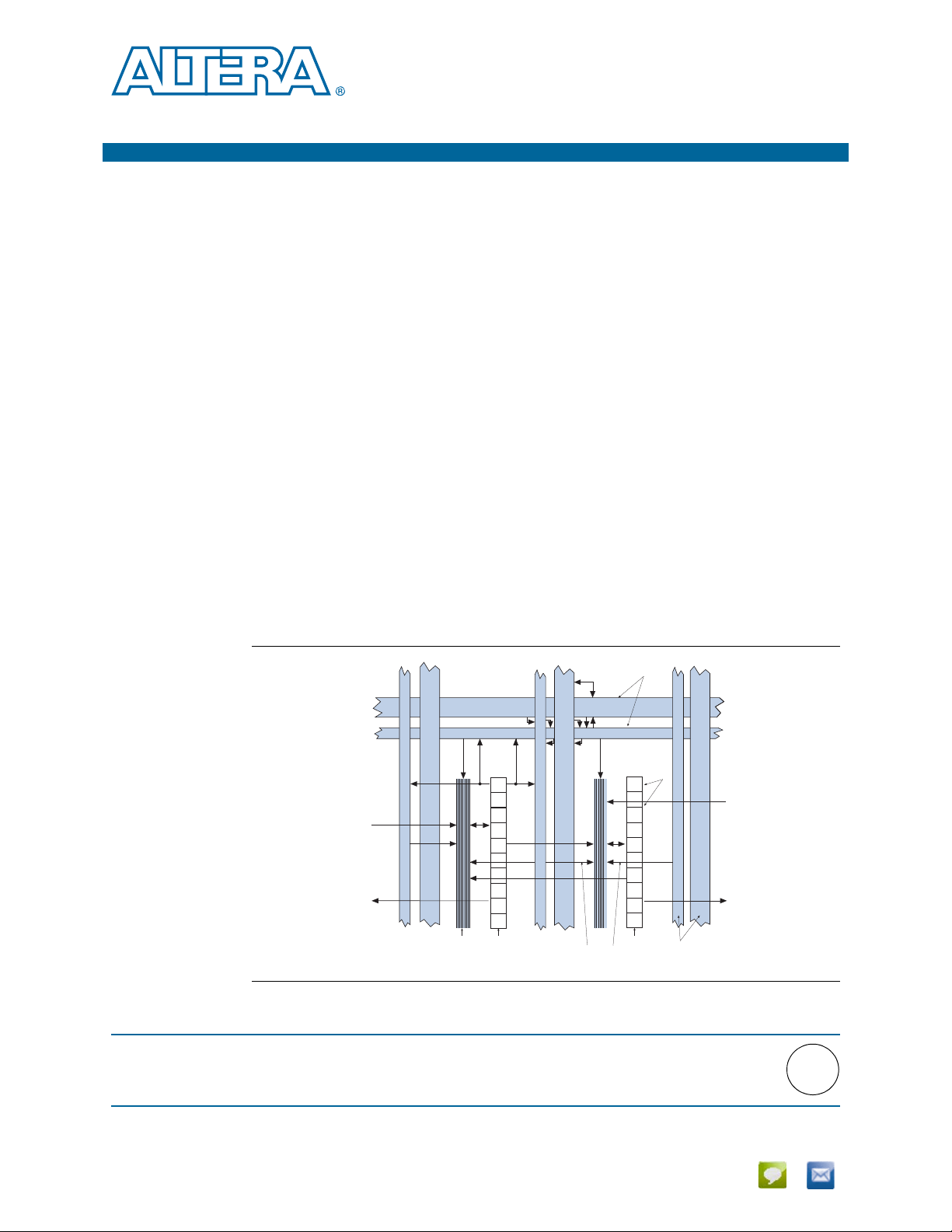
Each LAB consists of ten ALMs, various carry chains, shared arithmetic chains,
control signals, and a local interconnect. The local interconnect transfers signals
between ALMs in the same LAB. The direct link interconnect enables the LAB to drive
into the local interconnect of its left and right neighbors. The Quartus
places associated logic in the same LAB or adjacent LABs, allowing the use of local
and shared arithmetic chain for performance and area efficiency. Figure 1–1 shows the
Stratix V LAB structure and the LAB interconnects.
1. Logic Array Blocks and Adaptive Logic Modules in Stratix V Devices
®
II Compiler
Figure 1–1. LAB Structure for Stratix V Devices
© 2012 Altera Corporation. All rights reserved. ALTERA, ARRIA, CYCLONE, HARDCOPY, MAX, MEGACORE, NIOS, QUARTUS and STRATIX words and logos
are trademarks of Altera Corporation and registered in the U.S. Patent and Trademark Office and in other countries. All other words and logos identified as
trademarks or service marks are the property of their respective holders as described at www.altera.com/common/legal.html. Altera warrants performance of its
semiconductor products to current specifications in accordance with Altera's standard warranty, but reserves the right to make changes to any products and
services at any time without notice. Altera assumes no responsibility or liability arising out of the application or use of any information, product, or service
described herein except as expressly agreed to in writing by Altera. Altera customers are advised to obtain the latest version of device specifications before relying
on any published information and before placing orders for products or services.
ISO
9001:2008
Registered
Stratix V Device Handbook
Volume 1: Device Interfaces and Integration
June 2012
Feedback Subscribe
Page 16
1–2 Chapter 1: Logic Array Blocks and Adaptive Logic Modules in Stratix V Devices
MLAB
LAB
LUT-based-64 x 1
Simple dual-port SRAM
LUT-based-64 x 1
Simple dual-port SRAM
LUT-based-64 x 1
Simple dual-port SRAM
LUT-based-64 x 1
Simple dual-port SRAM
LUT-based-64 x 1
Simple dual-port SRAM
LUT-based-64 x 1
Simple dual-port SRAM
LUT-based-64 x 1
Simple dual-port SRAM
LUT-based-64 x 1
Simple dual-port SRAM
LUT-based-64 x 1
Simple dual-port SRAM
LUT-based-64 x 1
Simple dual-port SRAM
(1)
(1)
(1)
(1)
(1)
(1)
(1)
(1)
(1)
(1)
ALM
ALM
ALM
ALM
ALM
ALM
ALM
ALM
ALM
ALM
LAB Control Block
LAB Control Block
Logic Array Blocks
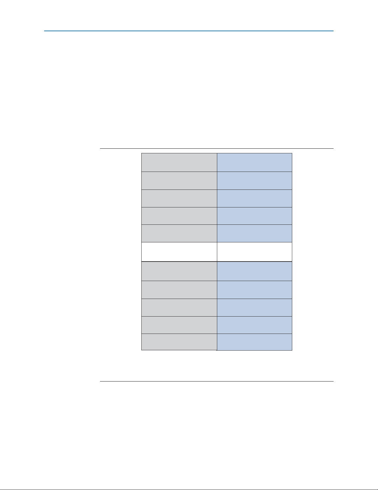
The memory LAB (MLAB) is a derivative of the Stratix V LAB. The MLAB adds
look-up table (LUT)-based SRAM capability to the LAB, as shown in Figure 1–2. The
MLAB supports a maximum of 640 bits of simple dual-port SRAM. You can configure
each ALM in an MLAB as either a 64 × 1 or a 32 × 2 block, resulting in a configuration
of either a 64 × 10 or a 32 × 20 simple dual-port SRAM block. MLAB and LAB blocks
alternate in Stratix V devices. Therefore, the maximum number of available MLABs is
half of the total number of LABs. The MLAB is a superset of the LAB and includes all
LAB features.
f For more information about MLABs, refer to the Memory Blocks in Stratix V Devices
chapter.
Figure 1–2. LAB and MLAB Structure for Stratix V Devices
Stratix V Device Handbook June 2012 Altera Corporation
Volume 1: Device Interfaces and Integration
Note to Figure 1–2:
(1) You can use the MLAB ALM as a regular LAB ALM or configure it as a dual-port SRAM.
Page 17
Chapter 1: Logic Array Blocks and Adaptive Logic Modules in Stratix V Devices 1–3
ALMs
Direct-link
interconnect
to right
Direct-link interconnect from the
right LAB, MLAB/M20K memory
block, DSP block, or IOE output
Direct-link interconnect from the
left LAB, MLAB/M20K memory
block, DSP block, or IOE output
Local
Interconnect
LAB
ALMs
Direct-link
interconnect
to left
MLAB
Logic Array Blocks
LAB Interconnects
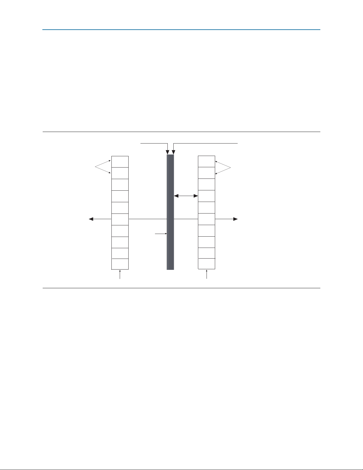
The LAB local interconnect can drive ALMs in the same LAB. It is driven by column
and row interconnects and ALM outputs in the same LAB. Neighboring
LABs/MLABs, M20K blocks, or digital signal processing (DSP) blocks from the left or
right can also drive the LAB’s local interconnect through the direct link connection.
The direct link connection feature minimizes the use of row and column
interconnects, providing higher performance and flexibility. Each LAB can drive
30 ALMs through fast-local and direct-link interconnects.
Figure 1–3 shows the direct-link connection.
Figure 1–3. Direct-Link Connection
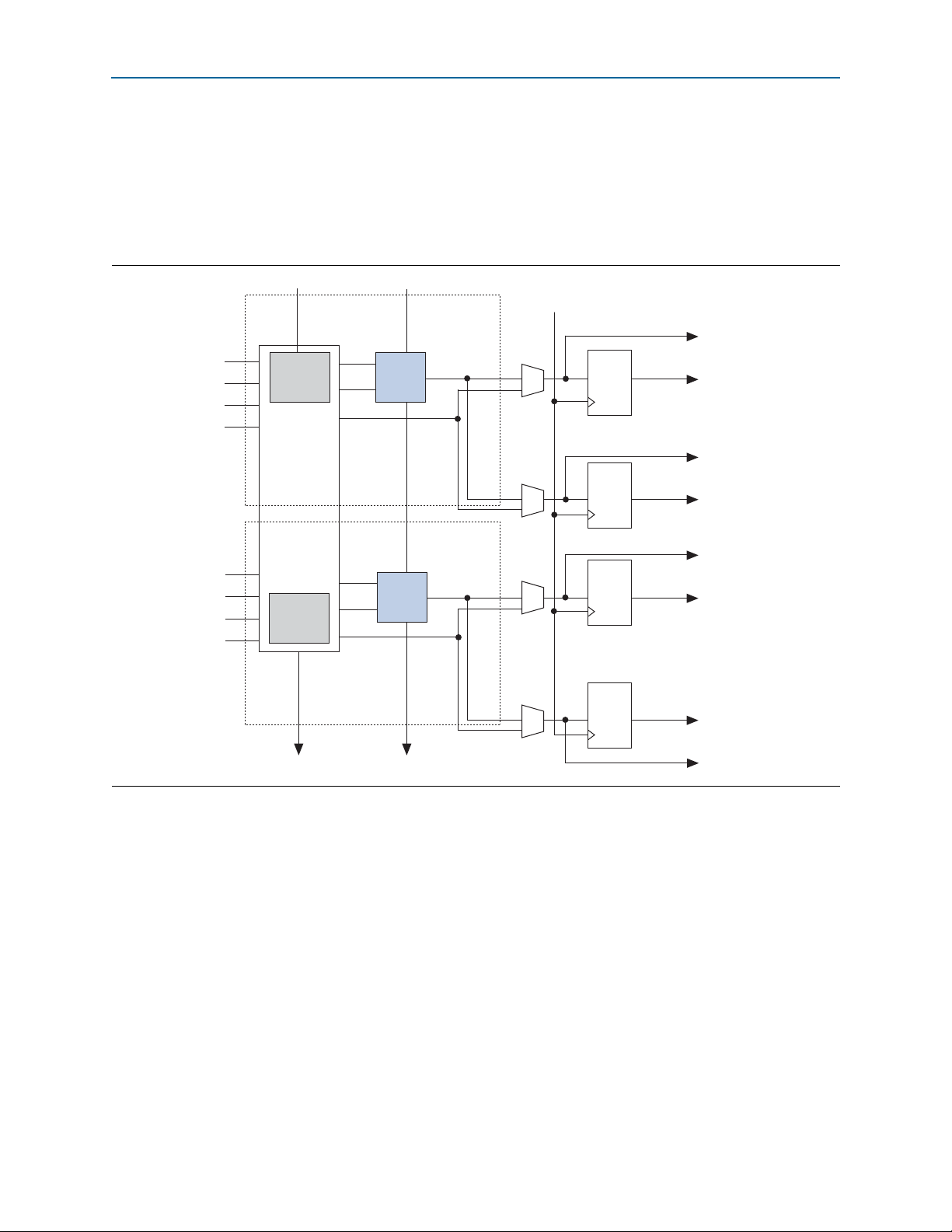
LAB Control Signals
Each LAB contains dedicated logic for driving control signals to its ALMs. The control
signals include three clocks, three clock enables, two asynchronous clears, one
synchronous clear, and one synchronous load, for a maximum of 10 control signals at
a time. Although you generally use synchronous load and clear signals when
implementing counters, you can also use them with other functions.
Each LAB has two unique clock sources and three clock enable signals, as shown in
Figure 1–4. The LAB control block can generate up to three clocks using two clock
sources and three clock enable signals. Each LAB’s clock and clock enable signals are
linked. For example, any ALM in a particular LAB using the
the
labclkena1
signal. If the LAB uses both the rising and falling edges of a clock, it
also uses two LAB-wide clock signals. Deasserting the clock enable signal turns off the
corresponding LAB-wide clock.
June 2012 Altera Corporation Stratix V Device Handbook
labclk1
Volume 1: Device Interfaces and Integration
signal also uses
Page 18
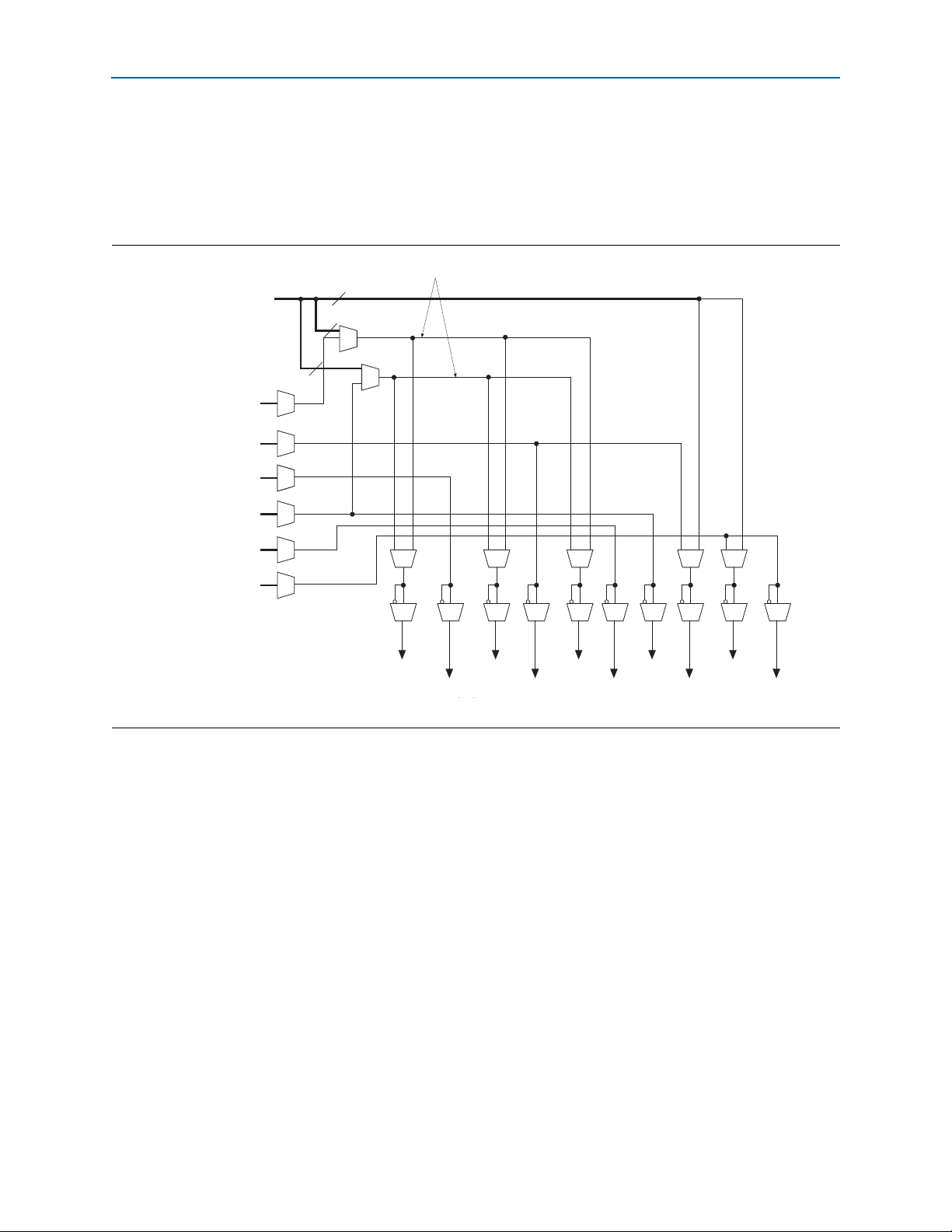
1–4 Chapter 1: Logic Array Blocks and Adaptive Logic Modules in Stratix V Devices
Dedicated Row LAB Clocks
Local Interconnect
Local Interconnect
Local Interconnect
Local Interconnect
Local Interconnect
Local Interconnect
labclk2
syncload
labclkena0
or asyncload
or labpreset
labclk0
labclk1
labclr1
labclkena1 labclkena2 labclr0 synclr
6
6
6
There are two unique
clock signals per LAB.
Adaptive Logic Modules
The LAB row clocks [5..0] and LAB local interconnects generate the LAB-wide control
signals. The MultiTrack interconnect’s inherent low skew allows clock and control
signal distribution in addition to data. The MultiTrack interconnect consists of
continuous, performance-optimized routing lines of different lengths and speeds used
for inter- and intra-design block connectivity.
Figure 1–4. LAB-Wide Control Signals
Adaptive Logic Modules
The ALM is the basic building block of logic in the Stratix V architecture. It provides
advanced features with efficient logic utilization. Each ALM contains a variety of
LUT-based resources that can be divided between two combinational adaptive LUTs
(ALUTs) and four registers. With up to eight inputs for the two combinational ALUTs,
one ALM can implement various combinations of two functions. This adaptability
allows an ALM to be completely backward-compatible with four-input LUT
architectures. One ALM can also implement any function with up to six inputs and
certain seven-input functions.
Stratix V Device Handbook June 2012 Altera Corporation
Volume 1: Device Interfaces and Integration
Page 19
Chapter 1: Logic Array Blocks and Adaptive Logic Modules in Stratix V Devices 1–5
datac
datad
datae1
dataf1
adder1
datae0
dataf0
dataa
datab
carry_in
carry_out
Combinational/Memory ALUT0
6-Input LUT
6-Input LUT
shared_arith_out
shared_arith_in
Combinational/Memory ALUT1
adder0
DQ
reg0
labclk
To general or
local routing
To general or
local routing
DQ
reg1
To general or
local routing
To general or
local routing
DQ
reg2
DQ
reg3
To general or
local routing
To general or
local routing
To general or
local routing
To general or
local routing
Adaptive Logic Modules
In addition to the adaptive LUT-based resources, each ALM contains four
programmable registers, two dedicated full adders, a carry chain, and a shared
arithmetic chain. Through these dedicated resources, an ALM can efficiently
implement various arithmetic functions and shift registers. Each ALM drives all types
of interconnects: local, row, column, carry chain, shared arithmetic chain, and direct
link. Figure 1–5 shows a high-level block diagram of the Stratix V ALM.
Figure 1–5. High-Level Block Diagram of the Stratix V ALM
June 2012 Altera Corporation Stratix V Device Handbook
Volume 1: Device Interfaces and Integration
Page 20
+
carry_in
dataf0
datae0
dataa
datab
datac1
datae1
dataf1
shared_arith_out carry_out
shared_arith_in
4-INPUT
LUT
4-INPUT
LUT
3-INPUT
LUT
3-INPUT
LUT
3-INPUT
LUT
3-INPUT
LUT
+
datac0
GND
V
CC
aclr[1:0]
sclr
syncload
clk[2:0]
D
Q
CLR
D
Q
CLR
row, column
direct link routing
D
Q
CLR
row, column
direct link routing
row, column
direct link routing
row, column
direct link routing
D
Q
CLR
3
3
Stratix V Device Handbook June 2012 Altera Corporation
Volume 1: Device Interfaces and Integration
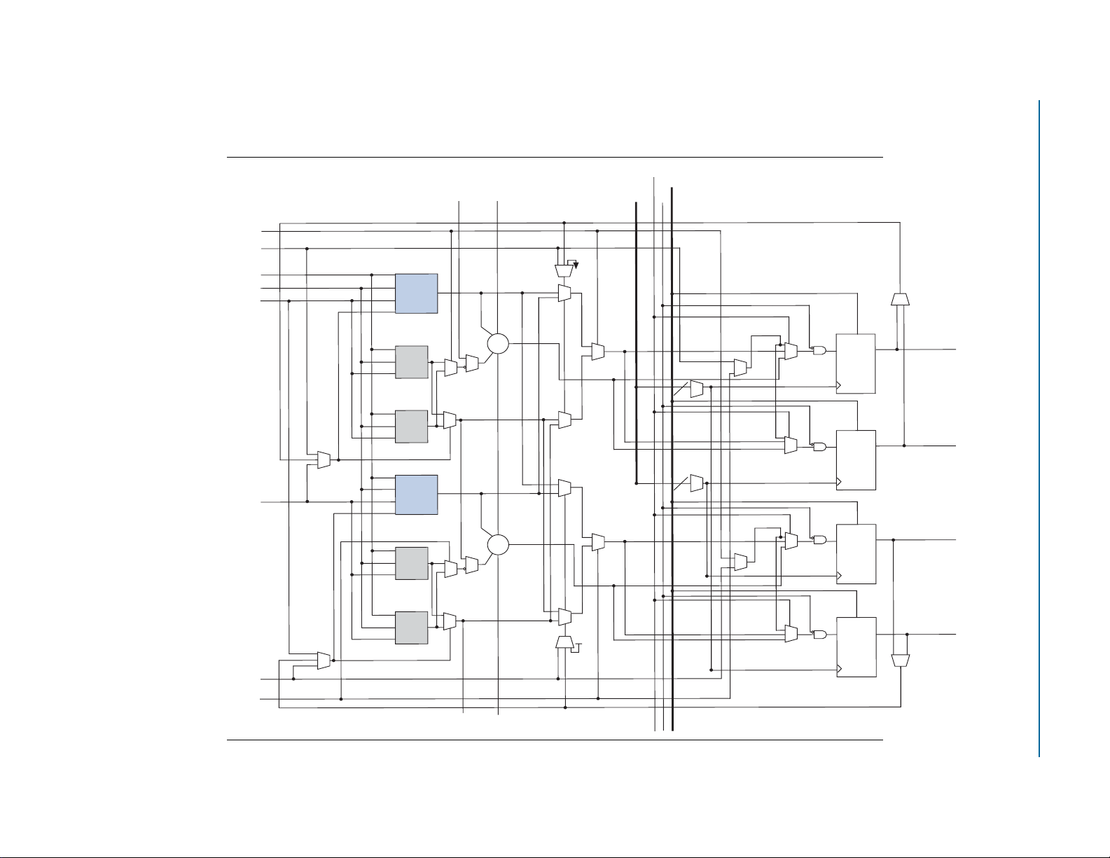
Figure 1–6 shows a detailed view of all the connections in an ALM.
Figure 1–6. ALM Connection Details for Stratix V Devices
1–6 Chapter 1: Logic Array Blocks and Adaptive Logic Modules in Stratix V Devices
Adaptive Logic Modules
Page 21

Chapter 1: Logic Array Blocks and Adaptive Logic Modules in Stratix V Devices 1–7
Adaptive Logic Modules
One ALM contains four programmable registers. Each register has data, clock,
synchronous and asynchronous clear, and synchronous load. Global signals,
general-purpose I/O pins, or any internal logic can drive the register’s clock and
clear-control signals. Either general-purpose I/O pins or internal logic can drive the
clock enable. For combinational functions, the register is bypassed and the output of
the LUT drives directly to the outputs of an ALM.
Each ALM has two sets of outputs that drive the local, row, and column routing
resources. The LUT, adder, or register outputs can drive these output drivers (refer to
Figure 1–6). For each set of output drivers, two ALM outputs can drive column, row,
or direct-link routing connections. One of these ALM outputs can also drive local
interconnect resources. This allows the LUT or adder to drive one output while the
register drives another output.
This feature, called register packing, improves device utilization because the device
can use the register and the combinational logic for unrelated functions. Another
special packing mode allows the register output to feed back into the LUT of the same
ALM so that the register is packed with its own fan-out LUT. This provides another
mechanism for improved fitting. The ALM can also drive out registered and
unregistered versions of the LUT or adder output.
ALM Operating Modes
The Stratix V ALM operates in one of the following modes:
■ “Normal Mode” on page 1–7
■ “Extended LUT Mode” on page 1–9
■ “Arithmetic Mode” on page 1–10
■ “Shared Arithmetic Mode” on page 1–11
Each mode uses ALM resources differently. In each mode, eleven available inputs to
an ALM—the eight data inputs from the LAB local interconnect, carry-in from the
previous ALM or LAB, and the shared arithmetic chain connection from the previous
ALM or LAB—are directed to different destinations to implement the desired logic
function. LAB-wide signals provide clock, asynchronous clear, synchronous clear,
synchronous load, and clock enable control for the register. These LAB-wide signals
are available in all ALM modes.
For more information about the LAB-wide control signals, refer to “LAB Control
Signals” on page 1–3.
The Quartus II software and supported third-party synthesis tools, in conjunction
with parameterized functions such as the library of parameterized modules (LPM)
functions, automatically choose the appropriate mode for common functions such as
counters, adders, subtractors, and arithmetic functions.
Normal Mode
Normal mode is suitable for general logic applications and combinational functions.
In this mode, up to eight data inputs from the LAB local interconnect are inputs to the
combinational logic. Normal mode allows two functions to be implemented in one
Stratix V ALM, or a single function of up to six inputs. The ALM can support certain
combinations of completely independent functions and various combinations of
functions that have common inputs.
June 2012 Altera Corporation Stratix V Device Handbook
Volume 1: Device Interfaces and Integration
Page 22
1–8 Chapter 1: Logic Array Blocks and Adaptive Logic Modules in Stratix V Devices
6-Input
LUT
dataf0
datae0
dataf0
datae0
dataa
datab
dataa
datab
datab
datac
datac
dataf0
datae0
dataa
datac
6-Input
LUT
datad
datad
datae1
combout0
combout1
combout0
combout1
combout0
combout1
dataf1
datae1
dataf1
datad
datae1
dataf1
4-Input
LUT
4-Input
LUT
4-Input
LUT
6-Input
LUT
dataf0
datae0
dataa
datab
datac
datad
combout0
5-Input
LUT
5-Input
LUT
dataf0
datae0
dataa
datab
datac
datad
combout0
combout1
datae1
dataf1
5-Input
LUT
dataf0
datae0
dataa
datab
datac
datad
combout0
combout1
datae1
dataf1
5-Input
LUT
3-Input
LUT
Adaptive Logic Modules
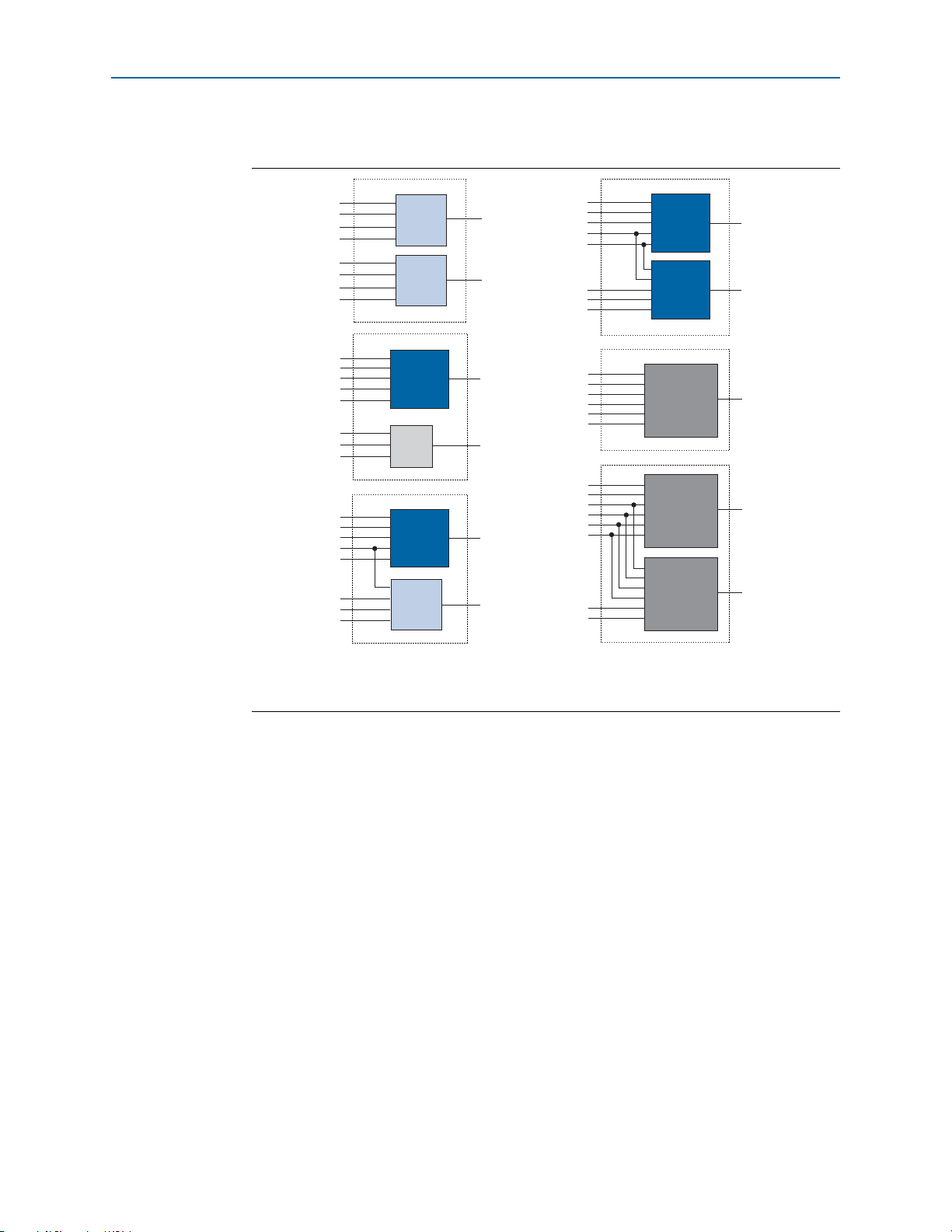
Figure 1–7 shows the supported LUT combinations in normal mode.
Figure 1–7. ALM in Normal Mode
(1)
Note to Figure 1–7:
(1) Combinations of functions with fewer inputs than those shown are also supported. For example, combinations of
functions with the following number of inputs are supported: 4 and 3, 3 and 3, 3 and 2, and 5 and 2.
Normal mode provides complete backward-compatibility with four-input LUT
architectures.
For the packing of 2 five-input functions into one ALM, the functions must have at
least two common inputs. The common inputs are
of a four-input function with a five-input function requires one common input (either
dataa
or
datab
In the case of implementing 2 six-input functions in one ALM, four inputs must be
shared and the combinational function must be the same. In a sparsely used device,
).
dataa
and
datab
. The combination
functions that could be placed in one ALM may be implemented in separate ALMs by
the Quartus II software to achieve the best possible performance. As a device begins
Stratix V Device Handbook June 2012 Altera Corporation
Volume 1: Device Interfaces and Integration
to fill up, the Quartus II software automatically uses the full potential of the Stratix V
ALM. The Quartus II Compiler automatically searches for functions using common
inputs or completely independent functions to be placed in one ALM to make efficient
use of device resources. In addition, you can manually control resource use by setting
location assignments.
Page 23

Chapter 1: Logic Array Blocks and Adaptive Logic Modules in Stratix V Devices 1–9
6-Input
LUT
dataf0
datae0
dataa
datab
datac
datad
datae1
dataf1
DQ
DQ
To general or
local routing
To general or
local routing
To general or
local routing
reg0
reg1
These inputs are available for register packing.
(2)
labclk
datae0
combout0
5-Input
LUT
5-Input
LUT
datac
dataa
datab
datad
dataf0
datae1
dataf1
DQ
To general or
local routing
To general or
local routing
reg0
This input is available
for register packing.
(1)
Adaptive Logic Modules
You can implement any six-input function using inputs
and either
output is either driven to
register0
datae0
and
register0
and
dataf0
or
datae1
and
dataf1
register0, register0
is bypassed, or the output driven to
is bypassed, and the data drives out to the interconnect
using the top set of output drivers (refer to Figure 1–8). If you use
the output either drives to
register1
or bypasses
dataa, datab, datac, datad
. If you use
datae0
and
datae1
register1
and drives to the
dataf0
and
dataf1
,
, the
interconnect using the bottom set of output drivers. The Quartus II Compiler
automatically selects the inputs to the LUT. ALMs in normal mode support register
packing.
Figure 1–8. Input Function in Normal Mode
Notes to Figure 1–8:
(1) If you use datae1 and dataf1 as inputs to a six-input function, datae0 and dataf0 are available for register
packing.
(2) The dataf1 input is available for register packing only if the six-input function is unregistered.
(1)
,
June 2012 Altera Corporation Stratix V Device Handbook
Extended LUT Mode
Use extended LUT mode to implement a specific set of seven-input functions. The set
must be a 2-to-1 multiplexer fed by two arbitrary five-input functions sharing four
inputs. Figure 1–9 shows the template of supported seven-input functions using
extended LUT mode. In this mode, if the seven-input function is unregistered, the
unused eighth input is available for register packing.
Functions that fit into the template shown in Figure 1–9 occur naturally in designs.
These functions often appear in designs as “if-else” statements in Verilog HDL or
VHDL code.
Figure 1–9. Template for Supported Seven-Input Functions in Extended LUT Mode
Note to Figure 1–9:
(1) If the seven-input function is unregistered, the unused eighth input is available for register packing. The second
register, reg1, is not available.
Volume 1: Device Interfaces and Integration
Page 24
1–10 Chapter 1: Logic Array Blocks and Adaptive Logic Modules in Stratix V Devices
Adaptive Logic Modules
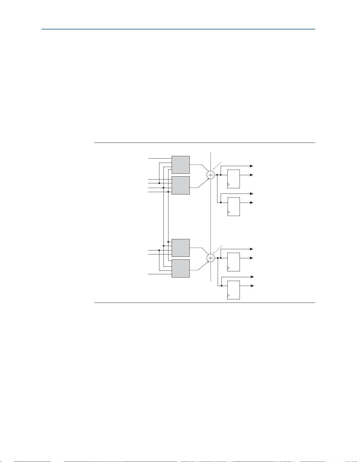
Arithmetic Mode
Arithmetic mode is ideal for implementing adders, counters, accumulators, wide
parity functions, and comparators. The ALM in arithmetic mode uses two sets of
2 four-input LUTs along with two dedicated full adders. The dedicated adders allow
the LUTs to be available to perform pre-adder logic; therefore, each adder can add the
output of 2 four-input functions.
The four LUTs share
signal feeds to
The carry-out from
adder0
adder1
dataa
and
datab
inputs. As shown in Figure 1–10, the carry-in
and the carry-out from
drives to
adder0
adder0
feeds to the carry-in of
adder1
of the next ALM in the LAB. ALMs in
arithmetic mode can drive out either registered, unregistered, or registered and
unregistered versions of the adder outputs.
Figure 1–10. ALM in Arithmetic Mode
carry_in
datae0
dataf0
datac
datab
dataa
datad
datae1
dataf1
4-Input
LUT
4-Input
LUT
4-Input
LUT
4-Input
LUT
carry_out
adder0
adder1
DQ
reg0
DQ
reg1
DQ
reg2
DQ
reg3
To general or
local routing
To general or
local routing
To general or
local routing
To general or
local routing
To general or
local routing
To general or
local routing
To general or
local routing
To general or
local routing
.
While operating in arithmetic mode, the ALM can support simultaneous use of the
adder’s carry output along with combinational logic outputs. In this operation, adder
output is ignored. Using the adder with combinational logic output provides resource
savings of up to 50% for functions that can use this ability.
Arithmetic mode also offers clock enable, counter enable, synchronous up/down
control, add/subtract control, synchronous clear, and synchronous load. The LAB
local interconnect data inputs generate the clock enable, counter enable, synchronous
up/down, and add/subtract control signals. These control signals are good
candidates for the inputs that are shared between the four LUTs in the ALM. The
synchronous clear and synchronous load options are LAB-wide signals that affect all
registers in the LAB. You can individually disable or enable these signals for each
register. The Quartus II software automatically places any registers that are not used
by the counter into other LABs.
Stratix V Device Handbook June 2012 Altera Corporation
Volume 1: Device Interfaces and Integration
Page 25

Chapter 1: Logic Array Blocks and Adaptive Logic Modules in Stratix V Devices 1–11
Adaptive Logic Modules
Carry Chain
The carry chain provides a fast carry function between the dedicated adders in
arithmetic or shared-arithmetic mode. The two-bit carry select feature in Stratix V
devices halves the propagation delay of carry chains within the ALM. Carry chains
can begin in either the first ALM or the fifth ALM in the LAB. The final carry-out
signal is routed to the ALM, where it is fed to local, row, or column interconnects.
The Quartus II Compiler automatically creates carry-chain logic during design
processing, or you can create it manually during design entry. Parameterized
functions such as LPM functions automatically take advantage of carry chains for the
appropriate functions.
The Quartus II Compiler creates carry chains longer than 20 (10 ALMs in arithmetic or
shared arithmetic mode) by linking LABs together automatically. For enhanced
fitting, a long carry chain runs vertically, allowing fast horizontal connections to
MLAB/M20K memory and DSP blocks. A carry chain can continue as far as a full
column.
To avoid routing congestion in one small area of the device when a high fan-in
arithmetic function is implemented, the LAB can support carry chains that only use
either the top half or bottom half of the LAB before connecting to the next LAB. This
leaves the other half of the ALMs in the LAB available for implementing narrower
fan-in functions in normal mode. Carry chains that use the top five ALMs in the first
LAB carry into the top half of the ALMs in the next LAB within the column. Carry
chains that use the bottom five ALMs in the first LAB carry into the bottom half of the
ALMs in the next LAB within the column. In every alternate LAB column, the top half
can be bypassed; in the other MLAB columns, the bottom half can be bypassed.
For more information about carry-chain interconnects, refer to “ALM Interconnects”
on page 1–13.
Shared Arithmetic Mode
In shared arithmetic mode, the ALM can implement a three-input add within the
ALM. In this mode, the ALM is configured with 4 four-input LUTs. Each LUT either
computes the sum of three inputs or the carry of three inputs. The output of the carry
computation is fed to the next adder (either to
the next ALM in the LAB) using a dedicated connection called the shared arithmetic
chain. This shared arithmetic chain can significantly improve the performance of an
adder tree by reducing the number of summation stages required to implement an
adder tree.
adder1
in the same ALM or to
adder0
of
June 2012 Altera Corporation Stratix V Device Handbook
Volume 1: Device Interfaces and Integration
Page 26
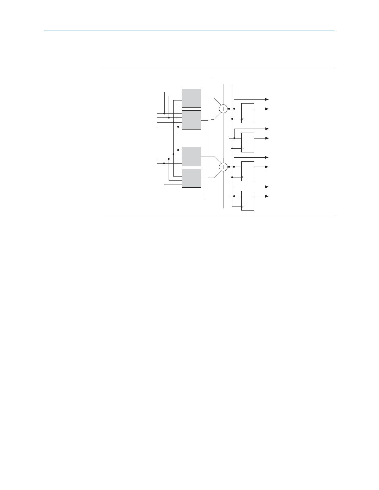
1–12 Chapter 1: Logic Array Blocks and Adaptive Logic Modules in Stratix V Devices
Adaptive Logic Modules
Figure 1–11 shows the ALM using this feature.
Figure 1–11. ALM in Shared Arithmetic Mode
shared_arith_in
carry_in
labclk
datae0
datac
datab
dataa
datad
datae1
4-Input
LUT
4-Input
LUT
4-Input
LUT
4-Input
LUT
shared_arith_out
DQ
reg0
DQ
reg1
DQ
reg2
DQ
reg3
carry_out
To general or
local routing
To general or
local routing
To general or
local routing
To general or
local routing
To general or
local routing
To general or
local routing
To general or
local routing
To general or
local routing
You can find adder trees in many different applications. For example, you can
implement the summation of the partial products in a logic-based multiplier in a tree
structure. Another example is a correlator function that can use a large adder tree to
sum filtered data samples in a given time frame to recover or de-spread data that was
transmitted using spread-spectrum technology.
Shared Arithmetic Chain
The shared arithmetic chain available in enhanced arithmetic mode allows the ALM
to implement a three-input add. This significantly reduces the resources necessary to
implement large adder trees or correlator functions.
The shared arithmetic chains can begin in either the first or sixth ALM in the LAB. The
Quartus II Compiler creates shared arithmetic chains longer than 20 (10 ALMs in
arithmetic or shared arithmetic mode) by linking LABs together automatically. For
enhanced fitting, a long shared arithmetic chain runs vertically, allowing fast
horizontal connections to the MLAB/M20K memory and DSP blocks. A shared
arithmetic chain can continue as far as a full column.
Similar to carry chains, the top and bottom halves of shared arithmetic chains in
alternate LAB columns can be bypassed. This capability allows the shared arithmetic
chain to cascade through half of the ALMs in a LAB while leaving the other half
available for narrower fan-in functionality. The top half of every other LAB column
can be bypassed, while the bottom half of the other LAB columns can be bypassed.
For more information on shared arithmetic chain interconnect, refer to “ALM
Interconnects” on page 1–13.
Stratix V Device Handbook June 2012 Altera Corporation
Volume 1: Device Interfaces and Integration
Page 27
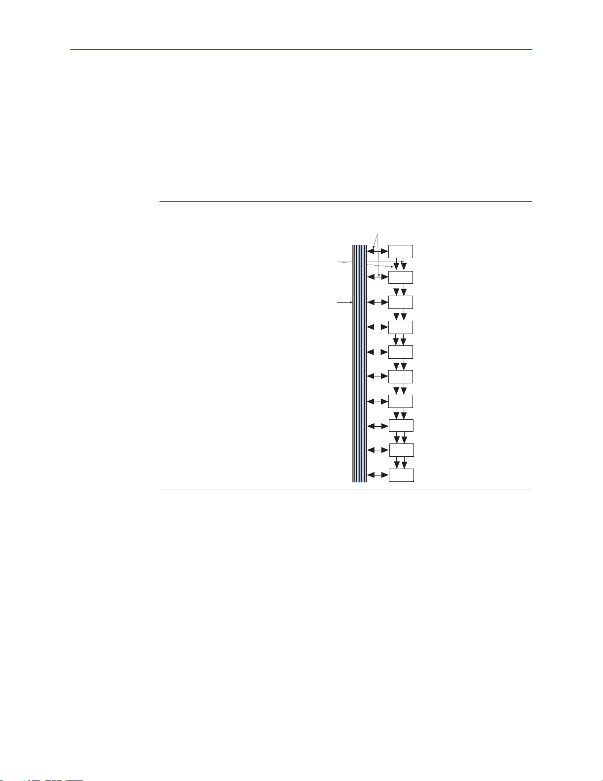
Chapter 1: Logic Array Blocks and Adaptive Logic Modules in Stratix V Devices 1–13
s
Adaptive Logic Modules
ALM Interconnects
There are two dedicated paths between ALMs—carry chain and shared arithmetic
chain. Stratix V devices include an enhanced interconnect structure in LABs for
routing shared arithmetic chains and carry chains for efficient arithmetic functions.
These ALM-to-ALM connections bypass the local interconnect. The Quartus II
Compiler automatically takes advantage of these resources to improve utilization and
performance. Figure 1–12 shows the shared arithmetic chain and carry chain
interconnects.
Figure 1–12. Shared Arithmetic Chain and Carry Chain Interconnects
Local interconnect
routing among ALM
in the LAB
Carry chain and shared
routing to adjacent ALM
Clear and Preset Logic Control
LAB-wide signals control the logic for the register’s clear signal. The ALM directly
supports an asynchronous clear function. You can achieve the register preset through
the Quartus II software’s NOT-gate push-back logic option. Each LAB supports up to
two clears.
arithmetic chain
Local
interconnect
ALM 1
ALM 2
ALM 3
ALM 4
ALM 5
ALM 6
ALM 7
ALM 8
ALM 9
ALM 10
Stratix V devices provide a device-wide reset pin (
DEV_CLRn
) that resets all the
registers in the device. An option set before compilation in the Quartus II software
controls this pin. This device-wide reset overrides all other control signals.
June 2012 Altera Corporation Stratix V Device Handbook
Volume 1: Device Interfaces and Integration
Page 28
1–14 Chapter 1: Logic Array Blocks and Adaptive Logic Modules in Stratix V Devices
Document Revision History
LAB Power Management Techniques
The following techniques are used to manage static and dynamic power consumption
within the LAB:
■ To save AC power, the Quartus II software forces all adder inputs low when the
ALM adders are not in use.
■ Stratix V LABs operate in high-performance mode or low-power mode. The
Quartus II software automatically chooses the appropriate mode for the LAB,
based on your design and to optimize speed versus leakage trade-offs.
■ Clocks represent a significant portion of dynamic power consumption because of
their high switching activity and long paths. The LAB clock that distributes a clock
signal to registers within a LAB is a significant contributor to overall clock power
consumption. Each LAB’s clock and clock enable signals are linked. For example, a
combinational ALUT or register in a particular LAB using the
uses the
labclkena1
signal. To disable a LAB-wide clock power consumption
without disabling the entire clock tree, use the LAB-wide clock enable to gate the
LAB-wide clock. The Quartus II software automatically promotes register-level
clock enable signals to the LAB-level. All registers within the LAB that share a
common clock and clock enable are controlled by a shared, gated clock. To take
advantage of these clock enables, use a clock-enable construct in your HDL code
for the registered logic.
labclk1
signal also
f For more information about implementing static and dynamic power consumption
within the LAB, refer to the Power Optimization chapter in volume 2 of the Quartus II
Handbook.
Document Revision History
Tab le 1 –1 lists the revision history for this chapter.
Table 1–1. Document Revision History
Date Version Changes
■ Updated Figure 1–5, Figure 1–6, and Figure 1–12.
June 2012 1.4
November 2011 1.3
May 2011 1.2
December 2010 1.1 No changes to the content of this chapter for the Quartus II software 10.1.
July 2010 1.0 Initial release.
■ Removed register chain expression.
■ Minor text edits.
■ Updated Figure 1–1, Figure 1–4, and Figure 1–6.
■ Removed “Register Chain” section.
■ Chapter moved to volume 2 for the 11.0 release.
■ Updated Figure 1–6.
■ Minor text edits.
Stratix V Device Handbook June 2012 Altera Corporation
Volume 1: Device Interfaces and Integration
Page 29
June 2012
SV51003-1.4
SV51003-1.4
2. Memory Blocks in Stratix V Devices
This chapter describes the embedded memory blocks in Stratix® V devices.
Embedded memory blocks provide different sizes of embedded SRAM to address the
Stratix V device design requirements efficiently. Embedded memory blocks include
640-bit enhanced memory logic array blocks (MLABs) and 20-Kbit M20K blocks.
MLABs are optimized to implement shift registers for digital signal processing (DSP)
applications, wide shallow FIFO buffers, and filter delay lines. You can use the M20K
blocks to support larger memory configurations and include error correction code
(ECC).
This chapter contains the following sections:
■ “Overview” on page 2–1
■ “Memory Modes” on page 2–10
■ “Clocking Modes” on page 2–17
■ “Design Considerations” on page 2–18
Overview
Tab le 2 –1 lists the features supported by the embedded memory blocks.
Table 2–1. Summary of Memory Features in Stratix V Devices (Part 1 of 2)
Feature MLABs M20K
Maximum performance 600 MHz 600 MHz
Total RAM bits (including parity bits) 640 20,480
16K x 1
8K x 2
64 x 8
64 x 9
Configurations (depth x width)
64 x 10
32 x 16
32 x 18
32 x 20
Parity bits Y Y
Byte enable Y Y
4K x 4
4K x 5
2K x 8
2K x 10
1K x 16
1K x 20
512 x 32
512 x 40
© 2012 Altera Corporation. All rights reserved. ALTERA, ARRIA, CYCLONE, HARDCOPY, MAX, MEGACORE, NIOS, QUARTUS and STRATIX words and logos
are trademarks of Altera Corporation and registered in the U.S. Patent and Trademark Office and in other countries. All other words and logos identified as
trademarks or service marks are the property of their respective holders as described at www.altera.com/common/legal.html. Altera warrants performance of its
semiconductor products to current specifications in accordance with Altera's standard warranty, but reserves the right to make changes to any products and
services at any time without notice. Altera assumes no responsibility or liability arising out of the application or use of any information, product, or service
described herein except as expressly agreed to in writing by Altera. Altera customers are advised to obtain the latest version of device specifications before relying
on any published information and before placing orders for products or services.
Stratix V Device Handbook
Volume 1: Device Interfaces and Integration
June 2012
Feedback Subscribe
ISO
9001:2008
Registered
Page 30

2–2 Chapter 2: Memory Blocks in Stratix V Devices
Overview
Table 2–1. Summary of Memory Features in Stratix V Devices (Part 2 of 2)
Feature MLABs M20K
Packed mode — Y
Address clock enable Y Y
Single-port memory Y Y
Simple dual-port memory Y Y
True dual-port memory — Y
Embedded shift register Y Y
ROM Y Y
FIFO buffer Y Y
Simple dual-port mixed width support — Y
True dual-port mixed width support — Y
Memory Initialization File (.mif)Y Y
Mixed-clock mode Y Y
Power-up condition
Outputs cleared if registered,
otherwise reads memory contents
Outputs cleared
Register clears Output registers Output registers
Write/Read operation triggering Write and Read—Rising clock edges Write and Read—Rising clock edges
Same-port read-during-write Outputs set to don’t care Outputs set to new data
Mixed-port read-during-write
(1)
ECC support
Notes to Table 2–1:
(1) You must use the same clock for both read and write ports. For more information, refer to “Mixed-Port Read-During-Write Mode” on
page 2–20.
(2) When you enable output register in the RAM MegaWizard Plug-In Manager in the Quartus II software, you can set the outputs to new data,
old data, don’t care, or constrained don’t care.
Outputs set to new data, old data,
don’t care, or constrained don’t
(2)
care
Soft IP support using the Quartus
software
Outputs set to old data or don’t care
Built-in support in x32-wide simple
II
dual-port mode or soft IP support
using the Quartus II software
Stratix V Device Handbook June 2012 Altera Corporation
Volume 1: Device Interfaces and Integration
Page 31

Chapter 2: Memory Blocks in Stratix V Devices 2–3
Overview
Tab le 2 –2 lists the capacity and distribution of the embedded memory blocks in each
Stratix V device.
Table 2–2. Memory Capacity and Distribution in Stratix V Devices
Family Device MLABs M20K Blocks
5SGXA3 6,415 957 19 22.92
5SGXA4 7,925 1,900 37 41.84
5SGXA5 9,250 2,304 45 50.65
5SGXA7 11,736 2,560 50 57.16
Stratix V GX
Stratix V GT
Stratix V GS
Stratix V E
5SGXA9 15,850 2,640 52 61.67
5SGXAB 17,960 2,640 52 62.96
5SGXB5 9,250 2,100 41 46.65
5SGXB6 11,270 2,660 52 58.88
5SGXB9 15,850 2,640 52 61.67
5SGXBB 17,960 2,640 52 62.96
5SGTC5 8,020 2,304 45 49.90
5SGTC7 11,736 2,560 50 57.16
5SGSD3 4,450 688 13 15.72
5SGSD4 6,792 957 19 23.15
5SGSD5 8,630 2,014 39 44.27
5SGSD6 11,000 2,320 45 51.71
5SGSD8 13,120 2,567 50 58.01
5SEE9 15,850 2,640 52 61.67
5SEEB 17,960 2,640 52 62.96
Total Dedicated RAM Bits
(M20K Blocks Only) (Mb)
Total RAM Bits (Including
LABs) (Mb)
Embedded Memory Block Types
M20K memory blocks are dedicated resources. MLABs are dual-purpose blocks. You
can configure the MLABs as regular logic array blocks (LABs) or as MLABs. Ten
adaptive logic modules (ALMs) make up one MLAB. You can configure each ALM in
an MLAB as either a 64 x 1 or a 32 x 2 block, resulting in a 64 x 10 or a 32 x 20 simple
dual-port SRAM block in a single MLAB.
Parity Bit Support
On MLABs, the ninth bit associated with each byte can store a parity bit or serve as an
additional data bit. No parity function is actually performed on the ninth bit.
The M20K supports one parity bit per 4-data bits when the data width is 5, 10, 20, or
40. The parity bits for inputs and outputs are bit 4, 9, 14, 19, 24, 29, 34, and 39. When
writing or reading with non-parity widths, these bits are skipped. No parity function
is performed on bit 4, 9, 14, 19, 24, 29, 34, and 39.
June 2012 Altera Corporation Stratix V Device Handbook
Volume 1: Device Interfaces and Integration
Page 32

2–4 Chapter 2: Memory Blocks in Stratix V Devices
Overview
Byte Enable Support
All embedded memory blocks support byte enables that mask the input data so that
only specific bytes of data are written. The unwritten bytes retain the previously
written values. The write enable (
signals, control the write operations of the RAM blocks.
The default value for the byte enable signals is high (enabled), in which case writing is
controlled only by the write enable signals. The byte enable registers do not have a
clear port. When using parity bits on the M20K blocks, the byte enable controls ten
bits (eight bits of data plus two parity bits). When using parity bits on the MLAB, the
byte enable controls all ten bits in the widest mode. Byte enables operate in a one-hot
fashion, with the LSB of the
The byte enables are active high.
wren
byteena
) signals, along with the byte enable (
byteena
)
signal corresponding to the LSB of the data bus.
Tab le 2 –3 lists the
Table 2–3. byteena Controls in x40 Data Width
byteena[3..0] Data Bits Written
1111(default)
1000
0100 —
0010 — —
0001 — — —
Tab le 2 –4 lists the
Table 2–4. byteena Controls in x20 Data Width
byteena[1:0] Data Bits Written
11(default)
byteena
byteena
10
01 —
controls in the x40 data width.
[39:30] [29:20] [19:10] [9:0]
[39:30]
———
[29:20]
controls in the x20 data width.
[19:10] [9:0]
[19:10]
——
[19:10]
[9:0]
—
[9:0]
—
1 If you use the ECC feature on the M20K blocks, you cannot use the byte enable
feature.
Stratix V Device Handbook June 2012 Altera Corporation
Volume 1: Device Interfaces and Integration
Page 33

Chapter 2: Memory Blocks in Stratix V Devices 2–5
inclock
wren
address
data
don't care: q (asynch)
byteena
XXXXXXXX XXXXXXXX
ABCDEF12
XXXX
1000 0100
0010 0001 1111 XXXX
an
a0 a1 a2
a3 a4 a0
FFFFEFFF
FFFFFFFF
FFFFFFFF
FFFFFFFF
FFFFFFFF
FFFFFFFF
ABFFFFFF
ABXXXXXX
FFCDFFFF
contents at a0
contents at a1
contents at a2
doutn
XXCDXXXX
XXXXEFXX XXXXXX12
ABFFFFFF
ABCDEF12
FFFFFF12
contents at a3
contents at a4
ABCDEF12
Overview
Figure 2–1 shows how the
RAM blocks. When a byte-enable bit is deasserted during a write cycle, the
corresponding data byte output can appear as either a “don’t care” value or the
current data at that location. The output value for the masked byte is controllable with
the Quartus II software. When a byte-enable bit is asserted during a write cycle, the
corresponding data byte output also depends on the setting chosen in the Quartus II
software.
Figure 2–1. Byte Enable Functional Waveform
wren
and
byteena
signals control the operations of the
Packed Mode Support
Stratix V M20K memory blocks support packed mode. The packed mode feature
packs two independent single-port RAMs into one memory block. The Quartus II
software automatically implements packed mode where appropriate by placing the
physical RAM block in true dual-port mode and using the MSB of the address to
distinguish between the two logical RAMs. The size of each independent single-port
RAM must not exceed half of the target block size.
Address Clock Enable Support
Stratix V embedded memory blocks support address clock enable, which holds the
previous address value for as long as the signal is enabled (
the memory blocks are configured in dual-port mode, each port has its own
independent address clock enable. The default value for the address clock enable
signal is low (disabled).
June 2012 Altera Corporation Stratix V Device Handbook
addressstall
Volume 1: Device Interfaces and Integration
= 1). When
Page 34

2–6 Chapter 2: Memory Blocks in Stratix V Devices
address[0]
address[N]
addressstall
clock
1
0
address[0]
register
address[N]
register
address[N]
address[0]
1
0
Overview
Figure 2–2 shows an address clock enable block diagram. The address clock enable is
referred to by the port name
addressstall
.
Figure 2–2. Address Clock Enable
Figure 2–3 shows the address clock enable waveform during the read cycle.
Figure 2–3. Address Clock Enable During Read Cycle Waveform
inclock
rdaddress
rden
addressstall
latched address
(inside memory)
q (synch)
q (asynch)
a0 a1 a2 a3 a4 a5
an a0
doutn-1 doutn
doutn
dout0
dout0
a1
dout1
dout1
a4
dout4
a6
a5
dout4
dout5
Stratix V Device Handbook June 2012 Altera Corporation
Volume 1: Device Interfaces and Integration
Page 35

Chapter 2: Memory Blocks in Stratix V Devices 2–7
Overview
Figure 2–4 shows the address clock enable waveform during the write cycle.
Figure 2–4. Address Clock Enable During the Write Cycle Waveform
inclock
wraddress
data
wren
addressstall
latched address
(inside memory)
contents at a0
contents at a1
contents at a2
a0 a1 a2 a3 a4 a5
00
an a0
XX
01 02
01XX
03 04
a1
00
02
XX
05
a4 a5
03
a6
06
contents at a3
contents at a4
contents at a5
XX
XX
XX
Mixed Width Support
M20K memory blocks support mixed data widths inherently. MLABs can support
mixed data widths through emulation with the Quartus II software. When using
simple dual-port, true dual-port, or FIFO modes, mixed width support allows you to
read and write different data widths to a memory block. For more information about
the different widths supported per memory mode, refer to “Memory Modes” on
page 2–10.
1 MLABs do not support mixed-width FIFO mode.
Asynchronous Clear
M20K memory blocks support asynchronous clear on output latches and output
registers. Therefore, if your RAM does not use output registers, clear the RAM
outputs using the output latch asynchronous clear. Because the clear is an
asynchronous signal, it is generated at any time. The internal logic extends the clear
pulse until the next rising edge of the output clock. When the clear is asserted, the
outputs are cleared and stay cleared until the next read cycle.
04
05
June 2012 Altera Corporation Stratix V Device Handbook
Volume 1: Device Interfaces and Integration
Page 36

2–8 Chapter 2: Memory Blocks in Stratix V Devices
clk
aclr
clr at
latch
out
D2
rden
D0 D1
Overview
Figure 2–5 shows the output latch clear in Stratix V devices.
Figure 2–5. Output Latch Clear in Stratix V Devices
Error Correction Code Support
M20K blocks have built-in support for ECC when in x32-wide simple dual-port mode.
ECC allows you to detect and correct data errors at the output of the memory. ECC
can perform single-error correction, double-adjacent-error correction, and
triple-adjacent-error detection in a 32-bit word; however, ECC cannot detect four or
more errors.
The M20K runs slower than non-ECC simple-dual port mode when ECC is engaged;
however, you can enable optional ECC pipeline registers before the output decoder to
achieve the same performance as non-ECC simple-dual port mode at the expense of
one cycle of latency.
The M20K ECC status is communicated with two ECC status flag signals—
and
ue
(uncorrectable error). The status flags are part of the regular output from the
memory block. When ECC is engaged, you cannot access two of the parity bits
because they are replaced by the ECC status flag.
e
(error)
Stratix V Device Handbook June 2012 Altera Corporation
Volume 1: Device Interfaces and Integration
Page 37

Chapter 2: Memory Blocks in Stratix V Devices 2–9
Input
Register
32
Memory
Array
ECC
Decoder
Status Flag
Generation
Output
Register
40
40
40
40
ECC
Encoder
8
32
Optional
Pipeline
Register
40
8
2
Overview
Tab le 2 –5 lists the truth table for the ECC status flags.
Table 2–5. Truth Table for the ECC Status Flags
e (error) ue (uncorrectable error) Status
00No error.
0 1 Illegal.
10
11
Note to Tab le 2–5:
(1)
eccstatus[1]
1 When ECC is engaged, you cannot use the byte enable feature. Also, when ECC is
engaged, read-during-write old data mode is not supported.
Figure 2–6 shows a diagram of the ECC block for M20K.
Figure 2–6. ECC Block for M20K
corresponds to e and
A correctable error occurred and the error has been
corrected at the outputs; however, the memory array
has not been updated.
An uncorrectable error occurred and uncorrectable
data appears at the outputs.
eccstatus[0]
(1)
corresponds to ue.
June 2012 Altera Corporation Stratix V Device Handbook
Volume 1: Device Interfaces and Integration
Page 38

2–10 Chapter 2: Memory Blocks in Stratix V Devices
Memory Modes
Memory Modes
Stratix V embedded memory blocks allow you to implement fully synchronous
SRAM memory in multiple modes of operation. M20K blocks do not support
asynchronous memory (unregistered inputs). MLABs support asynchronous
(flow-through) read operations.
Depending on which memory block you target, you can use the following modes:
■ “Single-Port RAM” on page 2–10
■ “Simple Dual-Port Mode” on page 2–12
■ “True Dual-Port Mode” on page 2–14 (only supported on M20K)
■ “Shift-Register Mode” on page 2–15
■ “ROM Mode” on page 2–16
■ “FIFO Mode” on page 2–16
1 If you use the memory blocks in ROM, single-port, simple dual-port, or true dual-port
mode, you can corrupt the memory contents if you violate the setup or hold-time on
any of the memory block input registers. This applies to both read and write
operations.
Single-Port RAM
All embedded memory blocks support single-port mode. Single-port mode allows
you to do either one-read or one-write operation at a time.
Figure 2–7 shows the single-port RAM configuration.
Figure 2–7. Single-Port RAM
Note to Figure 2–7:
(1) You can implement two single-port memory blocks in a single M20K block. For more information, refer to “Packed
Mode Support” on page 2–5.
During a write operation, the RAM output behavior is configurable. If you use the
read-enable signal and perform a write operation with the read enable deactivated,
the RAM outputs retain the values they held during the most recent active read
enable. If you activate read enable during a write operation or if you do not use the
read-enable signal at all, the RAM outputs show the “new data” being written.
(1)
data[]
address[]
wren
byteena[]
addressstall
inclock
clockena
rden
aclr
q[]
outclock
Stratix V Device Handbook June 2012 Altera Corporation
Volume 1: Device Interfaces and Integration
Page 39

Chapter 2: Memory Blocks in Stratix V Devices 2–11
A0
11
A1
A123 B456 C789 DDDD EEEE FFFF
clk_a
wren
rden
address
byteena
data_a
q_a (asynch)
A123 B456 C789 DDDD EEEE FFFF
Memory Modes
Tab le 2 –6 lists the possible port width configurations for embedded memory blocks in
single-port mode.
Table 2–6. Port Width Configurations for MLABs and M20K (Single-Port Mode)
Port Width Configurations
MLABs M20K
16K x 1
8K x 2
64 x 8
64 x 9
64 x 10
32 x 16
32 x 18
32 x 20
4K x 4
4K x 5
2K x 8
2K x 10
1K x 16
1K x 20
512 x 32
512 x 40
Figure 2–8 shows timing waveforms for read and write operations in single-port
mode with unregistered outputs. Registering the RAM outputs delay the
one clock cycle.
Figure 2–8. Timing Waveform for Read-Write Operations (Single-Port Mode)
q
output by
June 2012 Altera Corporation Stratix V Device Handbook
Volume 1: Device Interfaces and Integration
Page 40

2–12 Chapter 2: Memory Blocks in Stratix V Devices
Memory Modes
Simple Dual-Port Mode
All embedded memory blocks support simple dual-port mode. Simple dual-port
mode allows you to perform one-read and one-write operation to different locations
at the same time. The write operation happens on port A; the read operation happens
on port B. Figure 2–9 shows a simple dual-port configuration.
Figure 2–9. Simple Dual-Port Memory for Stratix V Devices
data[ ]
wraddress[ ]
wren
byteena[]
wr_addressstall
wrclock
wrclocken
Note to Figure 2–9:
(1) Simple dual-port RAM supports input/output clock mode and read/write clock mode.
rd_addressstall
(1)
rdaddress[ ]
rden
q[ ]
rdclock
rdclocken
ecc_status
aclr
Simple dual-port mode supports different read and write data widths (mixed-width
support). Tab le 2 –7 lists the mixed width configurations for M20K blocks in simple
dual-port mode. MLABs do not have native support for mixed-width operations. The
Quartus II software implements mixed-width memories in MLABs with more than
one MLAB.
Table 2–7. M20K Block Mixed-Width Configurations (Simple Dual-Port Mode)
Write Port
Read Port
16K x 1 8K x 2 4K x 4 4K x 5 2K x 8 2K x 10 1K x 16 1K x 20 512 x 32 512 x 40
16K x1Y Y Y—Y—Y—Y —
8Kx2 Y Y Y—Y—Y—Y —
4Kx4 Y Y Y—Y—Y—Y —
4K x5 ———Y—Y—Y— Y
2K x8 Y Y Y—Y—Y—Y —
2Kx10———Y—Y—Y— Y
1Kx16 Y Y Y—Y—Y—Y —
1Kx20———Y—Y—Y— Y
512x 32Y Y Y—Y—Y—Y —
512x 40———Y—Y—Y— Y
In simple dual-port mode, M20K blocks support separate write-enable and
read-enable signals. You can save power by keeping the read-enable signal low
(inactive) when not reading. Read-during-write operations to the same address can
either output a “don’t care” value or “old data” value. To choose the desired behavior,
set the read-during-write behavior to either don't care or old data in the RAM
MegaWizard Plug-In Manager. For more information, refer to “Read-During-Write
Behavior” on page 2–19.
Stratix V Device Handbook June 2012 Altera Corporation
Volume 1: Device Interfaces and Integration
Page 41

Chapter 2: Memory Blocks in Stratix V Devices 2–13
wrclock
wren
wraddress
rdclock
an-1
an
a0 a1 a2 a3 a4 a5
a6
q (asynch)
rden
rdaddress
bn
b0
b1 b2 b3
doutn-1 doutn
dout0
din-1 din din4 din5 din6
data
wrclock
wren
wraddress
rdclock
an-1
an
a0 a1 a2 a3 a4 a5
a6
q (asynch)
rden
rdaddress
bn
b0
b1 b2 b3
doutn-1 doutn
dout0
din-1 din din4 din5 din6
data
Memory Modes
MLABs only support a write-enable signal. Read-during-write behavior for the
MLABs can be a “new data”, “don’t care”, “old data”, or “constrained don’t care”
value. The available choices depend on the configuration of the MLAB.
Figure 2–10 shows timing waveforms for read and write operations in simple
dual-port mode with unregistered outputs. Registering the RAM outputs delay the
q
output by one clock cycle.
Figure 2–10. Simple Dual-Port Timing Waveforms
Figure 2–11 shows timing waveforms for read and write operations in mixed-port
mode with unregistered outputs.
Figure 2–11. Mixed-Port Read-During-Write Timing Waveforms
June 2012 Altera Corporation Stratix V Device Handbook
Volume 1: Device Interfaces and Integration
Page 42

2–14 Chapter 2: Memory Blocks in Stratix V Devices
Memory Modes
True Dual-Port Mode
Stratix V M20K blocks support true dual-port mode. Sometimes called bidirectional
dual-port, this mode allows you to perform any combination of two port
operations—two reads, two writes, or one read and one write at two different clock
frequencies.
Figure 2–12 shows the true dual-port RAM configuration.
Figure 2–12. True-Dual Port Memory for Stratix V Devices
data_a[]
address_a[]
wren_a
byteena_a[]
addressstall_a
clock_a
rden_a
aclr_a
q_a[]
data_b[]
address_b[]
wren_b
byteena_b[]
addressstall_b
clock_b
rden_b
aclr_b
q_b[]
The widest bit configuration of the M20K blocks in true dual-port mode is 1k x 16-bit
(x20-bit with parity).
Wider configurations are unavailable because the number of output drivers is
equivalent to the maximum bit width of the respective memory block. Because true
dual-port RAM has outputs on two ports, its maximum width equals half of the total
number of output drivers.
Tab le 2 –8 lists the possible M20K block mixed-port width configurations in true
dual-port mode.
Table 2–8. M20K Block Mixed-Width Configurations (True Dual-Port Mode)
Port B
Port A
16Kx1 8Kx2 4Kx4 4Kx5 2Kx8 2Kx10 1Kx16 1Kx20
16Kx1Y Y Y—Y—Y—
8Kx2 Y Y Y—Y—Y—
4Kx4 Y Y Y—Y—Y—
4Kx5———Y—Y—Y
2Kx8 Y Y Y—Y—Y—
2Kx10———Y—Y—Y
1Kx16Y Y Y—Y—Y—
1Kx20———Y—Y—Y
In true dual-port mode, M20K memory blocks support separate write-enable and
read-enable signals. You can save power by keeping the read-enable signal low
(inactive) when not reading. Read-during-write operations to the same address will
give you the “new data” output at that location. Set the read-during-write behavior to
new data in the RAM MegaWizard
Plug-In Manager in the Quartus II software. For
more information, refer to “Read-During-Write Behavior” on page 2–19.
Stratix V Device Handbook June 2012 Altera Corporation
Volume 1: Device Interfaces and Integration
Page 43

Chapter 2: Memory Blocks in Stratix V Devices 2–15
clk_a
wren_a
rden_a
address_a
clk_b
an-1
an a0 a1 a2 a3 a4 a5
a6
q_b (asynch)
wren_b
rden_b
address_b
bn
b0
b1 b2 b3
doutn-1
doutn
dout0
q_a (asynch)
din-1
din din4 din5
din6
data_a
din-1
din
dout0 dout1 dout2
dout3
din4
din5
dout2
dout1
Memory Modes
In true dual-port mode, you can access any memory location at any time from either
port. If you are accessing the same memory location from both ports, you must avoid
possible write conflicts. A write conflict happens if you are writing to the same
address location from both ports at the same time. This results in unknown data being
stored to that address location. No conflict resolution circuitry is built into the
Stratix V embedded memory blocks. You must resolve address conflicts external to
the RAM block.
Figure 2–13 shows true dual-port timing waveforms for the write operation at port A
and the read operation at port B, with the Read-During-Write behavior set to new
data. Registering the RAM outputs delay the
q
outputs by one clock cycle.
Figure 2–13. True Dual-Port Timing Waveform
Shift-Register Mode
All Stratix V memory blocks support shift register mode. Embedded memory block
configurations can implement shift registers for DSP applications, such as finite
impulse response (FIR) filters, pseudo-random number generators, multi-channel
filtering, and auto- and cross-correlation functions. These and other DSP applications
require local data storage, traditionally implemented with standard flipflops that
exhaust many logic cells for large shift registers. Alternatively, you can use embedded
memory as a shift-register block to save logic cell and routing resources.
The input data width (w), the length of the taps (m), and the number of taps (n)
determine the size of a shift register (w x m x n). You can cascade memory blocks to
implement larger shift registers.
June 2012 Altera Corporation Stratix V Device Handbook
Volume 1: Device Interfaces and Integration
Page 44

2–16 Chapter 2: Memory Blocks in Stratix V Devices
W
w × m × n Shift Register
m-Bit Shift Register
m-Bit Shift Register
m-Bit Shift Register
m-Bit Shift Register
W
W
W
W
W
W
W
n Number of Taps
Memory Modes
Figure 2–14 shows the embedded memory block in shift-register mode.
Figure 2–14. Shift-Register Memory Configuration
Stratix V Device Handbook June 2012 Altera Corporation
Volume 1: Device Interfaces and Integration
ROM Mode
All Stratix V embedded memory blocks support ROM mode. A .mif initializes the
ROM contents of these blocks. The address lines of the ROM are registered on M20K
blocks; however, they can be unregistered on MLABs. The outputs can be registered
or unregistered. Output registers can be asynchronously cleared. The ROM read
operation is identical to the read operation in the single-port RAM configuration.
FIFO Mode
All Stratix V embedded memory blocks support FIFO mode. MLABs are ideal for
designs with many small, shallow FIFO buffers. You can use the FIFO MegaWizard
Plug-In Manager to implement FIFO buffers in your design. The FIFO MegaWizard
Plug-In Manager supports single- and dual-clock (asynchronous) FIFO buffers.
f For more information about implementing FIFO buffers, refer to the SCFIFO and
DCFIFO Megafunctions User Guide.
1 MLABs do not support mixed-width FIFO mode.
Page 45

Chapter 2: Memory Blocks in Stratix V Devices 2–17
Clocking Modes
Clocking Modes
Stratix V embedded memory blocks support the following clocking modes:
■ “Independent Clock Mode” on page 2–17
■ “Input/Output Clock Mode” on page 2–17
■ “Read/Write Clock Mode” on page 2–17
■ “Single Clock Mode” on page 2–18
1 Violating the setup or hold time on the memory block address registers could corrupt
memory contents. This applies to both read and write operations.
Tab le 2 –9 lists the internal memory clock modes.
Table 2–9. Internal Memory Clock Modes
Clocking Mode True Dual-Port Mode Simple Dual-Port Mode Single-Port Mode ROM Mode FIFO Mode
Independent Y — — Y —
Input/output Y Y Y Y —
Read/write — Y — — Y
Single clock Y Y Y Y Y
Independent Clock Mode
Stratix V embedded memory blocks can implement independent clock mode for true
dual-port memories. In this mode, a separate clock is available for each port (clock A
and clock B). Clock A controls all registers on the port A side; clock B controls all
registers on the port B side. Each port also supports independent clock enables for
both port A and port B registers, respectively. Asynchronous clears are supported
only for output latches and output registers on both ports.
Input/Output Clock Mode
Stratix V embedded memory blocks can implement input/output clock mode for true
dual-port and simple dual-port memories. In this mode, an input clock controls all
registers related to the data input to the memory block including data, address, byte
enables, read enables, and write enables. An output clock controls the data output
registers. Asynchronous clears are available on output latches and output registers
only.
Read/Write Clock Mode
Stratix V embedded memory blocks can implement read/write clock mode for simple
dual-port memories. In this mode, a write clock controls the data-input,
write-address, and write-enable registers. Similarly, a read clock controls the
data-output, read-address, and read-enable registers. The memory blocks support
independent clock enables for both the read and write clocks. Asynchronous clears
are available on data output latches and registers only.
June 2012 Altera Corporation Stratix V Device Handbook
Volume 1: Device Interfaces and Integration
Page 46

2–18 Chapter 2: Memory Blocks in Stratix V Devices
When using read/write clock mode, if you perform a simultaneous read/write to the
same address location, the output read data is unknown. If you require the output
data to be a known value, use either single-clock mode or input/output clock mode
and choose the appropriate read-during-write behavior in the MegaWizard Plug-In
Manager.
Design Considerations
Single Clock Mode
Stratix V embedded memory blocks can implement single-clock mode for true
dual-port, simple dual-port, and single-port memories. In this mode, a single clock,
together with a clock enable, controls all registers of the memory block. Asynchronous
clears are available on output latches and output registers only.
Design Considerations
This section describes guidelines for designing with embedded memory blocks.
Selecting Embedded Memory Blocks
The Quartus II software automatically partitions user-defined memory into
embedded memory blocks by taking into account both speed and size constraints
placed on your design. For example, the Quartus II software may spread memory out
across multiple memory blocks when resources are available to increase the
performance of the design. You can manually assign memory to a specific block size
using the RAM MegaWizard Plug-In Manager.
MLABs can implement single-port SRAM through emulation with the Quartus II
software. Emulation results in minimal additional logic resources used. Because of the
dual-purpose architecture of the MLAB, it only has data input registers and output
registers in the block. MLABs gain read address registers from ALMs, while the write
address and read data registers are internal to MLAB.
f For more information about register packing, refer to the Logic Array Blocks and
Adaptive Logic Modules in Stratix V Devices chapter.
Conflict Resolution
When using memory blocks in true dual-port mode, you can perform two write
operations to the same memory location (address). Because there is no conflict
resolution circuitry in the memory blocks, you must implement conflict resolution
logic external to the memory block to avoid unknown data being written to the
address.
Stratix V Device Handbook June 2012 Altera Corporation
Volume 1: Device Interfaces and Integration
Page 47

Chapter 2: Memory Blocks in Stratix V Devices 2–19
Design Considerations
Read-During-Write Behavior
You can customize the read-during-write behavior of the Stratix V embedded
memory blocks to suit your design requirements. There are two types of
read-during-write operations—same port and mixed port.
Figure 2–15 shows the difference between the two types.
Figure 2–15. Read-During-Write Data Flow for Stratix V Devices
Port A
data in
Port A
data out
Port B
data in
Mixed-port
data flow
Same-port
data flow
Port B
data out
Same-Port Read-During-Write Mode
This mode applies to either a single-port RAM or the same port of a true dual-port
RAM. In same-port read-during-write mode, two output choices are available—new
data mode (or flow-through) or don’t care mode. If the MLAB is selected in same-port
read-during-write mode, only the don’t care mode is available. In new data mode, the
new data is available on the rising edge of the same clock cycle on which it was
written. In don’t care mode, the RAM outputs “don’t care” values for a
read-during-write operation.
Figure 2–16 shows sample functional waveforms of same-port read-during-write
behavior in new data mode.
Figure 2–16. Same-Port Read-During-Write—New Data Mode
clk_a
address
rden
wren
byteena
data_a
q_a (asynch)
June 2012 Altera Corporation Stratix V Device Handbook
A123 B456 C789 DDDD EEEE FFFF
A123 B456 C789 DDDD EEEE FFFF
0A 0B
11
Volume 1: Device Interfaces and Integration
Page 48

2–20 Chapter 2: Memory Blocks in Stratix V Devices
clk_a&b
address_a
wren_a
A0 A1
byteena_a
rden_b
11
data_a
AAAA BBBB CCCC DDDD EEEE FFFF
q_b (asynch)
A0(old data)
AAAA BBBB
A1(old data)
DDDD EEEE
address_b
A0 A1
Design Considerations
Mixed-Port Read-During-Write Mode
This mode applies to a RAM in simple or true dual-port mode that has one port
reading from and the other port writing to the same address location with the same
clock.
In this mode, you also have three output choices—”new data”, “old data”, or “don’t
care”. In old data mode, a read-during-write operation to different ports causes the
RAM outputs to reflect the “old data” value at that address location. In don’t care
mode, the same operation results in a “don’t care” or “unknown” value on the RAM
outputs.
f The RAM MegaWizard Plug-In Manager controls the read-during-write behavior. For
more information, refer to the Internal Memory (RAM and ROM) Megafunction User
Guide.
Figure 2–17 shows a sample functional waveform of mixed-port read-during-write
behavior for old data mode.
Figure 2–17. Mixed-Port Read-During-Write—Old Data Mode
Stratix V Device Handbook June 2012 Altera Corporation
Volume 1: Device Interfaces and Integration
Page 49

Chapter 2: Memory Blocks in Stratix V Devices 2–21
Design Considerations
Figure 2–18 shows a sample functional waveform of mixed-port read-during-write
behavior for don’t care mode.
Figure 2–18. Mixed-Port Read-During-Write—Don’t Care Mode
clk_a&b
wren_a
address_a
data_a
byteena_a
rden_b
address_b
q_b (asynch)
AAAA BBBB CCCC
11 01 10
A0 A1
DDDD EEEE FFFF
A0
XXXX (unknown data)
Mixed-port read-during-write is not supported if you use two different clocks in a
dual-port RAM. The output value is unknown during a dual-clock mixed-port
read-during-write operation.
Power-Up Conditions and Memory Initialization
The M20K memory block outputs power up to zero (cleared), regardless of whether
the output registers are used or bypassed. MLABs power up to zero if the output
registers are used and power up reading the memory contents if the output registers
are not used. You must consider this when designing logic that might evaluate the
initial power-up values of the MLAB memory block. For Stratix V devices, the
Quartus II software initializes the RAM cells to zero unless there is a .mif specified.
11
A1
All memory blocks support initialization with a .mif. You can create .mif files in the
Quartus II software and specify their use with the RAM MegaWizard Plug-In
Manager when instantiating a memory in your design. Even if a memory is
pre-initialized (for example, using a .mif), it still powers up with its outputs cleared.
f For more information about .mif files, refer to the Internal Memory (RAM and ROM)
Megafunction User Guide and the Quartus II Handbook.
Power Management
Stratix V memory block clock-enables allow you to control the clocking of each
memory block to reduce AC power consumption. Use the read-enable signal to
ensure that read operations only occur when you require read operations. If your
design does not require read-during-write, you can reduce your power consumption
by deasserting the read-enable signal during write operations, or any period when no
memory operations occur.
The Quartus II software automatically places any unused memory blocks in
low-power mode to reduce static power.
June 2012 Altera Corporation Stratix V Device Handbook
Volume 1: Device Interfaces and Integration
Page 50

2–22 Chapter 2: Memory Blocks in Stratix V Devices
Document Revision History
Document Revision History
Tab le 2 –1 0 lists the revision history for this chapter.
Table 2–10. Document Revision History
Date Version Changes
June 2012 1.4 Updated Table 2–1 and Table 2–2.
November 2011 1.3
May 2011 1.2
December 2010 1.1 No changes to the content of this chapter for the Quartus II software 10.1.
July 2010 1.0 Initial release.
■ Updated Table 2–1 and Table 2–2.
■ Updated “Mixed-Port Read-During-Write Mode” section.
■ Chapter moved to volume 2 for the 11.0 release.
■ Updated Table 2–1, Table 2–2, and Table 2–5.
■ Updated Figure 2–1 and Figure 2–8.
■ Updated “Read-During-Write Behavior” section.
■ Minor text edits.
Stratix V Device Handbook June 2012 Altera Corporation
Volume 1: Device Interfaces and Integration
Page 51

June 2012
SV51004-1.4
SV51004-1.4
3. Variable Precision DSP Blocks in Stratix V Devices
This chapter describes how the variable precision digital signal processing (DSP)
blocks in Stratix
®
V devices are optimized to support higher-bit precision in
high-performance DSP applications, such as radar systems that must support higher
resolution and multi-antenna architectures, wireless-base station channel cards for
multiple-input multiple-output (MIMO) processing, medical and test applications for
very high-precision filtering, and fast Fourier transforms (FFTs) functions.
You can configure a variable precision DSP block to implement one of several
operational modes to suit your application. The built-in pre-adder, coefficient bank,
multipliers, and adder/subtractor minimize the amount of external logic to
implement these functions, resulting in efficient resource usage, reduced power
consumption, improved performance, and data throughput for DSP applications.
A Stratix V variable precision DSP block maintains some backward compatibility
features, so it can efficiently support existing 18-bit DSP applications, such as
high-definition video processing, digital-up and down conversion, and multi-rate
filtering.
This chapter contains the following sections:
■ “Variable Precision DSP Block Overview” on page 3–1
■ “Operational Modes Overview” on page 3–3
■ “Variable Precision DSP Block Resource Descriptions” on page 3–4
■ “Operational Mode Descriptions” on page 3–9
■ “Software Support” on page 3–23
Variable Precision DSP Block Overview
Each Stratix V variable precision DSP block spans one logic array block (LAB) row
height.
The following are the architectural highlights of the Stratix V variable precision DSP
block:
■ High-performance, power-optimized, and fully registered multiplication
operations
■ Natively supported 9-bit, 18-bit, 27-bit, and 36-bit word lengths
■ Efficiently supported 18 x 25 complex multiplications for FFTs
■ Efficiently supported floating-point arithmetic formats
■ Built-in addition, subtraction, and 64-bit accumulation units to combine
multiplication results efficiently
© 2012 Altera Corporation. All rights reserved. ALTERA, ARRIA, CYCLONE, HARDCOPY, MAX, MEGACORE, NIOS, QUARTUS and STRATIX words and logos
are trademarks of Altera Corporation and registered in the U.S. Patent and Trademark Office and in other countries. All other words and logos identified as
trademarks or service marks are the property of their respective holders as described at www.altera.com/common/legal.html. Altera warrants performance of its
semiconductor products to current specifications in accordance with Altera's standard warranty, but reserves the right to make changes to any products and
services at any time without notice. Altera assumes no responsibility or liability arising out of the application or use of any information, product, or service
described herein except as expressly agreed to in writing by Altera. Altera customers are advised to obtain the latest version of device specifications before relying
on any published information and before placing orders for products or services.
ISO
9001:2008
Registered
Stratix V Device Handbook
Volume 1: Device Interfaces and Integration
June 2012
Feedback Subscribe
Page 52

3–2 Chapter 3: Variable Precision DSP Blocks in Stratix V Devices
■ Cascading 18-bit and 27-bit input bus to form tap-delay line for filtering
Variable Precision DSP Block Overview
applications
■ Cascading 64-bit output bus to propagate output results from one block to the next
block without external logic support
■ Hard pre-adder supported in 18-bit and 27-bit mode for symmetric filters
■ Supports 18-bit and 27-bit with internal coefficient register bank for filter
implementation
■ Efficiently supported 18-bit or 27-bit systolic finite impulse response (FIR) filters
with distributed output adder
Tab le 3 –1 lists the number of multipliers in Stratix V devices.
Table 3–1. Number of Multipliers in Stratix V Devices
Independent Input and Output
Multiplication Operators
Family
Stratix V GX
Stratix V GT
Stratix V GS
Stratix V E
Device
DSP Blocks
Variable Precision
9 × 9 Multipliers
16 × 16 Multipliers
18 × 18 Multipliers
27 × 27 Multipliers
with 32-Bit Resolution
36 × 18 Multipliers
Adder Mode
18 × 18 Multiplier
18 × 18 Multiplier
5SGXA3 256 768 512 512 256 256 512 256
5SGXA4 256 768 512 512 256 256 512 256
5SGXA5 256 768 512 512 256 256 512 256
5SGXA7 256 768 512 512 256 256 512 256
5SGXA9 352 1,056 704 704 352 352 704 352
5SGXAB 352 1,056 704 704 352 352 704 352
5SGXB5 399 1,197 798 798 399 399 798 399
5SGXB6 399 1,197 798 798 399 399 798 399
5SGXB9 352 1,056 704 704 352 352 704 352
5SGXBB 352 1,056 704 704 352 352 704 352
5SGTC5 256 768 512 512 256 256 512 256
5SGTC7 256 768 512 512 256 256 512 256
5SGSD3 600 1,800 1,200 1,200 600 600 1,200 600
5SGSD4 1,044 3,132 2,088 2,088 1,044 1,044 2,088 1,044
5SGSD5 1,590 4,770 3,180 3,180 1,590 1,590 3,180 1,590
5SGSD6 1,775 5,325 3,550 3,550 1,775 1,775 3,550 1,775
5SGSD8 1,963 5,889 3,926 3,926 1,963 1,963 3,926 1,963
5SEE9 352 1,056 704 704 352 352 704 352
5SEEB 352 1,056 704 704 352 352 704 352
Summed with 36-Bit input
Stratix V Device Handbook June 2012 Altera Corporation
Volume 1: Device Interfaces and Integration
Page 53

Chapter 3: Variable Precision DSP Blocks in Stratix V Devices 3–3
Operational Modes Overview
Operational Modes Overview
Tab le 3 –2 lists the summary of the operational modes that are supported by Stratix V
variable precision DSP blocks.
Table 3–2. Variable Precision DSP Blocks Operational Modes for Stratix V Devices
Variable Precision
DSP Block
Resources
1 variable precision
DSP block
Input
Cascade
support
Chainout
Support
Operational Mode
Supported
Instance
Pre-adder
Support
Coefficient
Support
Independent 9 x 9 Multiplication 3 No No No No
Independent 16 x 16 Multiplication 2 Yes Yes Yes No
Independent 18 x 18 Partial
Multiplication (32-Bit)
2 Yes Yes Yes No
Independent 18 x 18 Multiplication 1 Yes Yes Yes No
Independent 27 x 27 Multiplication 1 Yes Yes Yes Yes
Independent 36 x 18 Multiplication 1 No Yes No Yes
Two 18 x 18 Multiplier Adder 1 Yes Yes Yes Yes
Two 16 x 16 Multiplier Adder 1 Yes Yes Yes Yes
Sum of 2 Square 1 Yes
18 x 18 Multiplication Summed with
36-Bit Input
1NoNoNoYes
(1)
No No Yes
Independent 18 x 18 Multiplication 3 No No No No
Independent 36 x 36 Multiplication 1 No No No No
Complex 18 x 18 Multiplication 1 Yes Yes Yes Yes
2 variable precision
DSP blocks
Four 18 x 18 Multiplier Adder 1 Yes Yes Yes No
Two 27 x 27 Multiplier Adder 1 Yes Yes Yes No
Two 18 x 36 Multiplier Adder 1 No Yes No No
3 variable precision
DSP blocks
4 variable precision
DSP blocks
Note to Table 3–2:
(1) The pre-adder feature for this mode is automatically enabled.
Complex 18 x 25 Multiplication 1 Yes
Complex 27 x 27 Multiplication 1 Yes Yes Yes No
(1)
No No No
June 2012 Altera Corporation Stratix V Device Handbook
Volume 1: Device Interfaces and Integration
Page 54

3–4 Chapter 3: Variable Precision DSP Blocks in Stratix V Devices
Output Register Bank
COEFSELA[2..0]
COEFSELB[2..0]
+/-
Pre-Adder
+/-
Pre-Adder
+/-
Internal
Coefficient
Internal
Coefficient
Mult_L
Mult_H
Adder
+/-
Systolic
Registers
Systolic
Register
Chainout adder/
accumulator
+
chainin[63..0]
chainout[63..0]
Result[65..0]
x
x
datab_0[17..0]
dataa_0[17..0]
datab_1[17..0]
dataa_1[17..0]
18
18
18
18
64
ACCUMULATE
LOADCONST
NEGATE
SUB
Constant
CLK[2..0]
ENA[2..0]
ACLR[1..0]
scanin [17..0]
Input Register Bank
scanout[17..0]
+/-
Variable Precision DSP Block Resource Descriptions
The QuartusII software includes megafunctions that you can use to control the
operation mode of the multipliers. After making the appropriate parameter settings
with the MegaWizard
Plug-In Manager, the Quartus II software automatically
configures the variable precision DSP block.
Variable Precision DSP Block Resource Descriptions
The Stratix V variable precision DSP block consists of the following elements:
■ Input register bank
■ Pre-adder and coefficient select
■ Multipliers
■ Chainout adder and accumulator
■ Systolic registers
■ Output register bank
Figure 3–1 shows a detailed overall architecture of the 18 x 18 Stratix V variable
precision DSP block.
Figure 3–1. 18 x 18 Variable Precision DSP Block Architecture for Stratix V Devices
Stratix V Device Handbook June 2012 Altera Corporation
Volume 1: Device Interfaces and Integration
Page 55

Chapter 3: Variable Precision DSP Blocks in Stratix V Devices 3–5
Output Register Bank
COEFSELA[2..0]
Pre-Adder
+/-
Internal
Coefficient
Multiplier
Chainout adder/
accumulator
+
chainin[63..0]
chainout[63..0]
Result[65..0]
x
datab_0[26..0]
dataa_0[26..0]
27
27
datac_0[24..0]
25
64
ACCUMULATE
LOADCONST
NEGATE
Constant
CLK[2..0]
ENA[2..0]
ACLR[1..0]
scanin [26..0]
Input Register Bank
scanout[26..0]
+/-
Variable Precision DSP Block Resource Descriptions
Figure 3–2 shows a detailed overall architecture of the 27 x 27 Stratix V variable
precision DSP block.
Figure 3–2. 27 x27 Variable Precision DSP Block Architecture for Stratix V Devices
Input Registers Bank
The positive edge of the clock signal triggers all variable precision DSP block registers
and clears them after power up. Each multiplier operand can feed an input register or
a multiplier directly, bypassing the input registers. The following variable precision
DSP block signals control the input registers within the variable precision DSP block:
■
CLK[2..0]
■
ENA[2..0]
■
ACLR[0]
Besides the registers for the data and dynamic control signals, there are also two sets
of delay registers in the input register bank. The delay registers are used to balance the
latency requirements when both the input cascade and chainout features are used.
This is only supported in 18 x 18 mode.
June 2012 Altera Corporation Stratix V Device Handbook
Volume 1: Device Interfaces and Integration
Page 56

3–6 Chapter 3: Variable Precision DSP Blocks in Stratix V Devices
datab_0[17..0]
dataa_0[17..0]
datab_1[17..0]
Delay registers
dataa_1[17..0]
Delay registers
scanin[17..0]
scanout[17..0]
CLK[2..0]
ENA[2..0]
ACLR[0]
Variable Precision DSP Block Resource Descriptions
One feature of the input register bank is to support a tap delay line; therefore, you can
drive the top leg of the multiplier input (B) from general routing or from the cascade
chain, as shown in Figure 3–3 and Figure 3–4. The Stratix V variable precision DSP
block supports 18-bit and 27-bit input cascading.
Figure 3–3. Input Register of a Variable Precision DSP Block in 18 x 18 Mode for Stratix V Devices
Note to Figure 3–3:
(1) Figure 3–3 shows only the data registers. Registers for the control signals are not shown.
Stratix V Device Handbook June 2012 Altera Corporation
Volume 1: Device Interfaces and Integration
Page 57

Chapter 3: Variable Precision DSP Blocks in Stratix V Devices 3–7
Variable Precision DSP Block Resource Descriptions
Figure 3–4. Input Register of a Variable Precision DSP Block in 27 x 27 Mode for Stratix V
Devices
CLK[2..0]
ENA[2..0]
scanin[26..0]
datab_0[26..0]
dataa_0[26..0]
datac_0[24..0]
ACLR[0]
Note to Figure 3–4:
(1) Figure 3–4 shows only the data registers. Registers for the control signals are not shown.
Pre-Adder and Coefficient Select
The pre-adder supports both addition and subtraction, which you must choose
during compilation time. There are two 18-bit pre-adders in each variable precision
DSP block. You can configure these two pre-adders as two independent 18-bit adders
for 18-bit applications, or a 26-bit adder for 27-bit applications.
The Stratix V variable precision DSP block has the flexibility of selecting the
multiplicand from either the dynamic input or internal coefficient. The internal
coefficient can support up to eight constant coefficients for the multiplicands in 18-bit
and 27-bit applications. When you enable the internal coefficient feature, the
COEFSELA/COEFSELB
multiplexer.
In 18-bit applications, you must enable the coefficient feature when the pre-adder
feature is enabled. In 27-bit applications, you can use the coefficient feature and
pre-adder feature independently. In 27-bit applications with the pre-adder feature
enabled, the input data width is restricted to 22 bits if the multiplicand input comes
from dynamic input due to input limitations. If the multiplicand input comes from
internal coefficient, the data width of the input is 27 bits.
are used to control the dynamic selection of the coefficient
scanout[26..0]
1 When you enable the pre-adder feature, all input data must have the same clock
setting.
June 2012 Altera Corporation Stratix V Device Handbook
Volume 1: Device Interfaces and Integration
Page 58

3–8 Chapter 3: Variable Precision DSP Blocks in Stratix V Devices
Variable Precision DSP Block Resource Descriptions
Multipliers
There are two multipliers (Mult_H and Mult_L) per variable precision DSP block. You
can configure these two multipliers to work as a 27 x 27 multiplier, two 18 x 18
multipliers, or three 9 x 9 multipliers, depending on the operational mode. A single
variable precision DSP block can perform many multiplications in parallel, depending
on the data width of the multiplier. For more information, refer to “Operational Mode
Descriptions” on page 3–9.
Chainout Adder and Accumulator
The accumulator feature is not available in multi-block modes.
The Stratix V variable precision DSP blocks contain a 64-bit adder and a 64-bit
accumulator. You can use the 64-bit adder as full adder.
Tab le 3 –3 lists the functions supported by the accumulator in Stratix V devices.
Table 3–3. Functions Supported by Accumulator in Stratix V Devices
Function Description
Zeroing Disables the accumulator.
Preload
Accumulation Adds the current result to the previous accumulate result.
Decimation
Loads an initial value to the accumulator. Only 1 bit of the 64-bit preload value can be “1”. It
can be used as rounding the DSP result to any position of the 64-bit result.
This function takes the current result, converts it into two’s compliment, and adds it to the
previous result.
You can dynamically control the function of the accumulator by three control
signals—
signals control the accumulator functions.
Table 3–4. Dynamic Control Signals for 64-Bit Accumulator for Stratix V Devices
Function NEGATE LOADCONST ACCUMULATE
Accumulate 0 0 1
Decimate 1 0 1
Preload 0 1 0
Systolic Register
There are two systolic registers per variable precision DSP block. The first systolic
register has two 18-bit registers that are used to register the Mult_L’s two 18-bit
inputs. You must clock these registers with the same clock source as the output
register bank. The second systolic register is used to delay the
next variable precision DSP block. If the variable precision DSP block is not
configured in systolic FIR mode, both systolic registers are bypassed.
NEGATE, LOADCONST
Zero 0 0 0
, and
ACCUMULATE
. Table 3–4 lists how these dynamic
chainout
output to the
Stratix V Device Handbook June 2012 Altera Corporation
Volume 1: Device Interfaces and Integration
Page 59

Chapter 3: Variable Precision DSP Blocks in Stratix V Devices 3–9
Operational Mode Descriptions
Output Register Bank
The positive edge of the clock signal triggers the 64-bit bypassable output register
bank and is cleared after power up. The following variable precision DSP block
signals control the output register per variable precision DSP block:
■
CLK[2..0]
■
ENA[2..0]
■
ACLR[1]
Operational Mode Descriptions
This section describes how you can configure a Stratix V variable precision DSP block
to efficiently support the following operational modes:
■ “Independent Multiplier Modes” on page 3–9
■ “Independent Complex Multiplier Modes” on page 3–14
■ “Multiplier Adder Sum Mode” on page 3–17
■ “Sum of Square Mode” on page 3–20
■ “18 x 18 Multiplication Summed with 36-Bit Input Mode” on page 3–20
■ “Systolic FIR Mode” on page 3–21
Independent Multiplier Modes
In independent input and output multiplier mode, the variable precision DSP blocks
perform individual multiplication operations for general purpose multipliers.
9 x 9, 16 x 16, 18 x18, 27 x 27, and 36 x 18 Multipliers
You can configure each variable precision DSP block multiplier for 9-, 16-, 18-, 27-bit,
or 36 x 18 multiplication. A variable precision DSP block can support up to three
individual 9 x 9 multipliers, two individual 16 × 16 multipliers, two individual 18 x 18
partial multipliers, one individual 18 x 18 multiplier, one individual 27 x 27
multiplier, or one individual 36 x 18 multiplier. For some operational modes, the
unused inputs require zero padding.
June 2012 Altera Corporation Stratix V Device Handbook
Volume 1: Device Interfaces and Integration
Page 60

3–10 Chapter 3: Variable Precision DSP Blocks in Stratix V Devices
result[35..0]
Output Register Bank
dataa_0[17..0]
datab_0[17..0]
Mult_L
Variable Precision DSP Block
x
36
18
18
Input Register Bank
Operational Mode Descriptions
Figure 3–5, Figure 3–6, Figure 3–8 on page 3–12, Figure 3–9 on page 3–12, and
Figure 3–10 on page 3–13 show the variable precision DSP block in independent
multiplier operation mode. Figure 3–7 on page 3–11 shows that two variable precision
DSP blocks can support three individual 18 x 18 multipliers.
Figure 3–5. Three 9 x 9 Independent Multiplier Mode for Stratix V Devices
ay[y2, y1, y0]
27
27
ax[x2, x1, x0]
Input Register Bank
Variable Precision DSP Block
Multiplier
x
(1)
54
result[53..0]
(p2, p1, p0)
Output Register Bank
Note to Figure 3–5:
(1) Three pairs of data are packed into the ax and ay ports; result contains three 18-bit products.
Figure 3–6. One 18 x 18 Independent Multiplier Mode with One Variable Precision DSP Block for Stratix V Devices
Stratix V Device Handbook June 2012 Altera Corporation
Volume 1: Device Interfaces and Integration
Page 61

Chapter 3: Variable Precision DSP Blocks in Stratix V Devices 3–11
datab_0[17..0]
dataa_0[17..0]
dataa_2[17..0]
dataa_2[17..0]
datab_2[17..0]
datab_2[17..0]
datab_1[17..0]
dataa_1[17..0]
Variable Precision DSP Block 1
Variable Precision DSP Block 2
result_0[35..0]
result_1[35..0]
result_2[17..0]
result_2[35..18]
Mult_L
Input Register Bank
Output Register Bank
x
Mult_H
Mult_L
x
x
Mult_H
x
Output Register Bank
18
36
18
18
36
18
18
18
18
18
18
18
Input Register Bank
Operational Mode Descriptions
Figure 3–7. Three 18 x 18 Independent Multiplier Mode with Two Variable Precision DSP Blocks for Stratix V Devices
June 2012 Altera Corporation Stratix V Device Handbook
Volume 1: Device Interfaces and Integration
Page 62

3–12 Chapter 3: Variable Precision DSP Blocks in Stratix V Devices
Operational Mode Descriptions
Figure 3–8. Two 16 x 16 Independent Multiplier Mode or Two 18 x 18 Independent Partial Multiplier Mode for Stratix V
Devices
(1), (2)
datab_0[ ]
dataa_0[ ]
datab_1[ ]
dataa_1[ ]
Input Register Bank
Variable Precision DSP Block
Mult_L
x
Mult_H
x
result_0[ ]
Output Register Bank
result_1[ ]
Notes to Figure 3–8:
(1) The inputs for 16-bit independent multiplier mode are
data[15..0]
. The unused input bits require padding with zero.
(2) For 18-bit independent multiplier mode, only 32-LSB output for both multipliers are routed to the output register.
Figure 3–9. One 27 x 27 Independent Multiplier Mode for Stratix V Devices
(1)
Multiplier
dataa_b0[26..0]
dataa_a0[26..0]
27
x
27
Input Register Bank
Variable Precision DSP Block
Note to Figure 3–9:
(1) The result can be up to 64-bits when combined with a chainout adder/accumulator.
54
Output Register Bank
Result[53..0]
Stratix V Device Handbook June 2012 Altera Corporation
Volume 1: Device Interfaces and Integration
Page 63

Chapter 3: Variable Precision DSP Blocks in Stratix V Devices 3–13
Output Register Bank
dataa_0[35..18]
datab_0[17..0]
datab_0[17..0]
dataa_0[17..0]
result[53..0]
Mult_L
x
Mult_H
Variable Precision DSP Block
+
x
Input Register Bank
18
18
18
18
54
datab_0[17..0]
dataa_0[17..0]
dataa_0[35..18]
datab_0[17..0]
datab_0[35..18]
dataa_0[17..0]
datab_0[35..18]
dataa_0[35..18]
Variable Precision DSP Block 1
Variable Precision DSP Block 2
result[17..0]
result[71..18]
18
18
18
18
18
54
18
18
18
18
Mult_H
x
Mult_L
x
x
Mult_H
x
Mult_L
x
Adder
Adder
+
+
Input Register Bank
Input Register Bank
Output Register BankOutput Register Bank
Operational Mode Descriptions
Figure 3–10. One 36 × 18 Independent Multiplier Mode for Stratix V Devices
36-Bit Multiplier
You can efficiently construct an individual 36-bit multiplier with two adjacent
Stratix V variable precision DSP blocks. The 36 x 36 multiplication consists of four
18 x 18 multipliers, as shown in Figure 3–11. The 36-bit multiplier is useful for
applications requiring more than 18-bit precision; for example, for the mantissa
multiplication portion of very high precision fixed-point arithmetic applications.
Figure 3–11. 36-Bit Independent Multiplier Mode with Two Variable Precision DSP Blocks for Stratix V Devices
June 2012 Altera Corporation Stratix V Device Handbook
Volume 1: Device Interfaces and Integration
Page 64

3–14 Chapter 3: Variable Precision DSP Blocks in Stratix V Devices
37
37
c
b
a
b
d
d
c
a
Variable Precision DSP Block 1
Variable Precision DSP Block 2
18
18
18
18
18
18
18
18
Output Register Bank
Output Register Bank
Mult_L
x
Mult_L
x
(ad + bc)
Imaginary part
(ac - bd)
Real part
Adder
+
Adder
-
Mult_H
x
Mult_H
x
Input Register BankInput Register Bank
Operational Mode Descriptions
Independent Complex Multiplier Modes
The Stratix V variable precision DSP block provides the means for a complex
multiplication. Equation 3–1 shows a complex multiplication that you can write.
Equation 3–1. Complex Multiplication Equation
(a + jb) × (c + jd) = [(a × c) - (b × d)] + j[(a × d) + (b × c)]
The Stratix V variable precision DSP block can support an 18 x 18 complex multiplier,
18 x 25 complex multiplier, or a 27 x 27 complex multiplier.
18 x 18 Complex Multiplier
For 18 x 18 complex multiplications, you require two variable precision DSP blocks to
perform this multiplication mode. You can implement the imaginary part [(a × d) +
(b × c)] in the first variable precision DSP block, and you can implement the real part
[(a × c) – (b × d)] in the second variable precision DSP block.
Figure 3–12 shows an 18-bit complex multiplication.
Figure 3–12. 18 x 18 Complex Multiplier with Two Variable Precision DSP Blocks for Stratix V Devices
Stratix V Device Handbook June 2012 Altera Corporation
Volume 1: Device Interfaces and Integration
Page 65

Chapter 3: Variable Precision DSP Blocks in Stratix V Devices 3–15
Variable Precision DSP Block 1
Chainout
Adder
Chainout
Adder
+
Variable Precision DSP Block 2
Variable Precision DSP Block 3
[(c + d) b + (a - b) d]
[(c - d) a + (a - b) d]
d[17..0]
a[24..0]
b[24..0]
b[24..0]
c[17..0]
d[17..0]
c[17..0]
d[17..0]
a[24..0]
44
44
Input Register BankInput Register Bank
Input Register Bank
Pre-adder &
Coefficient Select
Pre-adder &
Coefficient Select
Pre-adder &
Coefficient Select
x
Multiplier
x
Multiplier
Multiplier
x
x
Output Register BankOutput Register Bank
25
25
18
18
18
18
18
25
25
+
Operational Mode Descriptions
18 x 25 Complex Multiplier
Stratix V devices support an individual 18 x 25 complex multiplication mode. A
27 x 27 multiplier allows you to implement an individual 18 x 25 complex
multiplication mode with three variable precision DSP blocks only. The pre-adder
feature is automatically enabled for you to implement an individual 18 x 25 complex
multiplication mode efficiently.
You can implement an 18 x 25 complex multiplication with three variable precision
DSP blocks, as shown in Equation 3–2.
Equation 3–2. 18 × 25 Complex Multiplication Equation
(a + jb) × (c + jd) = (c - d) × a + (a - b) × d + j [(c + d) × b + (a - b) × d]
Figure 3–13 shows an 18 x 25 complex multiplication with three variable precision
DSP blocks.
Figure 3–13. 18 x 25 Complex Multiplier with Three Variable Precision DSP Blocks for Stratix V Devices
June 2012 Altera Corporation Stratix V Device Handbook
Volume 1: Device Interfaces and Integration
Page 66

3–16 Chapter 3: Variable Precision DSP Blocks in Stratix V Devices
[(a × d) + (b × c)]
b[26..0]
a[26..0]
b[26..0]
a[26..0]
d[26..0]
c[26..0]
c[26..0]
d[26..0]
Variable Precision DSP Block 1
Variable Precision DSP Block 2
Variable Precision DSP Block 3
[(a × c) - (b × d)]
Output Register Bank
Variable Precision DSP Block 4
55
55
Multiplier
x
Multiplier
x
Multiplier
x
Multiplier
x
+
Output Register Bank
Chainout
Adder
Chainout
Adder
+
Input Register Bank
Input Register Bank
Input Register Bank
Input Register Bank
27
27
27
27
27
27
27
27
Operational Mode Descriptions
27 x 27 Complex Multiplier
Stratix V devices support an individual 27 x 27 complex multiplication mode. You
require four variable precision DSP blocks to implement an individual 27 x 27
complex multiplication mode. You can implement the imaginary part
[(a × d) + (b × c)] in the first and second variable precision DSP blocks, and you can
implement the real part [(a × c) - (b × d)] in the third and fourth variable precision
DSP blocks. You can achieve the difference of two 27 × 27 multiplications by enabling
the
NEGATE
Figure 3–14 shows a 27-bit complex multiplication with four variable precision DSP
blocks.
Figure 3–14. 27 × 27 Complex Multiplier with Four Variable Precision Blocks
control signal in the fourth variable precision DSP block.
Stratix V Device Handbook June 2012 Altera Corporation
Volume 1: Device Interfaces and Integration
Page 67

Chapter 3: Variable Precision DSP Blocks in Stratix V Devices 3–17
Operational Mode Descriptions
Multiplier Adder Sum Mode
Stratix V devices support two-multiplier adder sum mode and four-multiplier adder
sum mode. For a two-multiplier adder configuration, the Stratix V variable precision
DSP blocks can support 16-bit, 18-bit, 27-bit, and 18 × 36 multipliers. You require two
variable precision DSP blocks to implement 27-bit and 18 x 36 multiplier adder sum
mode. Stratix V devices support one sum of four 18-bit multipliers with two variable
precision DSP blocks. Figure 3–15 through Figure 3–18 show the variable precision
DSP blocks in the multiplier adder sum mode.
Figure 3–15. One Sum of Two 18 x 18 Multipliers or Two 16 x 16 Multipliers for Stratix V Devices
SUB
datab_0[ ]
dataa_0[ ]
datab_1[ ]
dataa_1[ ]
Input Register Bank
Mult_L
x
+/-
Mult_H
x
Adder
(1), (2)
Result[]
Output Register Bank
Notes to Figure 3–15:
(1) For 18-bit multiplier adder sum mode, the input data width is 18 bits and the output data width is 37 bits.
(2) For 16-bit multiplier adder sum mode, the input data width is 16 bits and the unused input bit requires padding with zeroes. The output data width
is 33 bits.
June 2012 Altera Corporation Stratix V Device Handbook
Volume 1: Device Interfaces and Integration
Page 68

3–18 Chapter 3: Variable Precision DSP Blocks in Stratix V Devices
Variable Precision DSP Block 2
Variable Precision DSP Block 1
Multiplier
x
Result[54..0]
55
Output Register Bank
x
+
Multiplier Chainout adder
Chainout[53..0]
dataa_0[26..0]
datab_0[26..0]
dataa_1[26..0]
NEGATE
datab_1[26..0]
Input Register Bank
Input Register Bank
27
27
27
27
+/-
+
Operational Mode Descriptions
Figure 3–16. One Sum of Two 27 x 27 Multipliers with Two Variable Precision DSP Blocks for Stratix V Devices
Figure 3–17. One Sum of Two 36 x 18 Multipliers with Two Variable Precision DSP Blocks for Stratix V Devices
Multiplier
x
Input Register Bank
Multiplier
Chainout
Adder
x
Input Register Bank
+/-
54
result[54..0]
Output Register Bank
datab_0[17..0]
dataa_0[17..0]
datab_0[17..0]
dataa_0[35..18]
datab_1[17..0]
dataa_1[17..0]
datab_1[17..0]
dataa_1[35..18]
NEGATE
18
18
18
18
Variable Precision DSP Block 1
18
18
18
18
Variable Precision DSP Block 2
Stratix V Device Handbook June 2012 Altera Corporation
Volume 1: Device Interfaces and Integration
Page 69

Chapter 3: Variable Precision DSP Blocks in Stratix V Devices 3–19
result[37..0]
Input Register Bank
19
18
Variable Precision DSP Block 1
19
18
Mult_L
Mult_H
Adder
SUB
19
18
Variable Precision DSP Block 2
19
38
18
SUB
Chainout[38..0]
x
x
+/-
Input Register Bank
Output Register Bank
Mult_L
Mult_H
Adder
Chainout adder
x
x
+/- +
dataa_1[17..0]
datab_2[17..0]
datab_3[17..0]
dataa_3[17..0]
NEGATE
datab_1[17..0]
dataa_0[17..0]
datab_0[17..0]
dataa_2[17..0]
+/-
Operational Mode Descriptions
Figure 3–18. One Sum of Four 18 x 18 Multipliers with Two Variable Precision DSP Blocks for Stratix V Devices
June 2012 Altera Corporation Stratix V Device Handbook
Volume 1: Device Interfaces and Integration
Page 70

3–20 Chapter 3: Variable Precision DSP Blocks in Stratix V Devices
Multiplier
result[36..0]
b[17..0]
a[17..0]
Multiplier
x
Adder
Pre-Adder
d[17..0]
SUB
c[17..0]
+/-
Pre-Adder
Variable Precision DSP Block
+/-
+/-
Input Register Bank
Output Register Bank
18
37
18
18
18
x
data_1[35..18]
data_1[17..0]
dataa_0[17..0]
datab_0[17..0]
Input Register Bank
Result[36..0]
Variable Precision DSP Block
37
18
18
18
18
Mult_L
Adder
SUB
Output Register Bank
x
+/-
Operational Mode Descriptions
Sum of Square Mode
The Stratix V variable precision DSP block can implement one sum of square mode,
2
(a ± b)
convert
required. You can feed each 18-bit pre-adder block output into both multiplicand and
multiplier inputs of an 18 x 18 multiplier to generate a square result.
Figure 3–19 shows the sum of square mode in a variable precision DSP block.
Figure 3–19. One Sum of Square Mode in a Variable Precision DSP Block for Stratix V Devices
×(c±d) 2. You can feed the four 18-bit inputs into the pre-adder block to
b
and d input as two’s complement numbers to perform subtraction, if
Figure 3–20. One 18 × 18 Multiplication Summed with 36-Bit Input Mode for Stratix V Devices
Stratix V Device Handbook June 2012 Altera Corporation
Volume 1: Device Interfaces and Integration
18 x 18 Multiplication Summed with 36-Bit Input Mode
Stratix V variable precision DSP blocks support one 18 x 18 multiplication summed to
a 36-bit input. You can use Mult_L to provide the input for an 18 x 18 multiplication,
whereas Mult_H is bypassed. The
concatenated to produce a 36-bit input. Figure 3–20 shows the 18 x 18 multiplication
summed with the 36-bit input mode in a variable precision DSP block.
data1[17..0]
and
data1[35..18]
signals are
Page 71

Chapter 3: Variable Precision DSP Blocks in Stratix V Devices 3–21
Input Register Bank
Output Register Bank
COEFSELA[2..0]
COEFSELB[2..0]
+/-
Pre-Adder
+/-
Pre-Adder
+/-
Internal
Coefficient
Internal
Coefficient
Mult_L
Mult_H
Adder
+/-
Systolic
Registers
Systolic
Register
Chainout adder/
accumulator
+
chainin[43..0]
chainout[43..0]
Result[43..0]
18-bit Systolic FIR
x
x
datab_0[17..0]
dataa_0[17..0]
datab_1[17..0]
dataa_1[17..0]
18
18
18
18
3
44
3
Input Register Bank
COEFSELA[2..0]
Pre-Adder
+/-
Internal
Coefficient
Multiplier
Chainout adder or
accumulator
+
chainin[63..0]
chainout[63..0]
27-bit Systolic FIR
27
x
Output Register Bank
datab_0[26..0]
dataa_0[26..0]
datac_0[24..0]
Operational Mode Descriptions
Systolic FIR Mode
Stratix V variable precision DSP blocks support 18-bit and 27-bit systolic FIR
structures. In systolic FIR mode, the input of the multiplier can come from three
different sets of sources:
■ two dynamic inputs
■ one dynamic input and once coefficient input
■ one coefficient input and one pre-adder output
Figure 3–21 shows the 18-bit systolic FIR with two dynamic inputs. In 18-bit systolic
FIR mode, the adders are configured as dual 44-bit adders, thereby giving 8 bits of
overhead when using an 18-bit operation (36-bit products). This allows a total sum of
256 multiplier products.
Figure 3–21. 18-bit Systolic FIR Mode with Two Dynamic Inputs for Stratix V Devices
Figure 3–22 shows the 27-bit systolic FIR. This mode allows the implementation of
one stage systolic filter per DSP block. The chainout adder or accumulator is
configured for a 64-bit operation, providing 10 bits of overhead when using a 27-bit
data (54-bit products). This allows a total sum of 1,024 multiplier products.
Figure 3–22. 27-bit Systolic FIR Mode for Stratix V Devices
Volume 1: Device Interfaces and Integration
June 2012 Altera Corporation Stratix V Device Handbook
Page 72

3–22 Chapter 3: Variable Precision DSP Blocks in Stratix V Devices
Operational Mode Descriptions
Variable Precision DSP Block Control Signals
The Stratix V variable precision DSP block has a total of 14 dynamic control signal
inputs. The variable precision DSP block dynamic signals are user-configurable and
can be set to toggle or not at run time.
Table 3–5 on page 3–22 lists the variable precision DSP block dynamic signals. The
Stratix V variable precision DSP block supports 18-bit and 27-bit input cascading.
Table 3–5. Variable Precision DSP Block Dynamic Signals for Stratix V Devices
Signal Name Function Count
NEGATE
LOADCONST
ACCUMULATE
SUB
COEFSELA
COEFSELB
CLK0
CLK1
CLK2
ENA0
ENA1
ENA2
ACLR0
ACLR1
Control the operation of the decimation 1
Preload an initial value to the accumulator 1
Enable accumulation 1
This signal has two functions:
■ Controls add or subtract of the two 18 x 18 multiplier results
■ Controls dynamic switch between 36 x 36 mode and complex 18 x 18
Controls the internal coefficient select multiplexer along with select signals
provided through the MSB of each 18-bit data input
Variable precision DSP-block-wide clock signals 3
Variable precision DSP-block-wide clock enable signals 3
Variable precision DSP-block-wide asynchronous clear signals 2
Total Count per DSP Block 14
1
2
Stratix V Device Handbook June 2012 Altera Corporation
Volume 1: Device Interfaces and Integration
Page 73

Chapter 3: Variable Precision DSP Blocks in Stratix V Devices 3–23
Software Support
Software Support
Altera provides two methods for implementing various modes of the
Stratix V variable precision DSP block in a design—using the Quartus II DSP
megafunction and HDL inferring.
The following Quartus II megafunctions are supported for the
Stratix V variable precision DSP blocks implementation:
■ LPM_MULT
■ ALTMULT_ADD
■ ALTMULT_ACCUM
■ ALTMULT_COMPLEX
Alternatively, you can infer the Stratix V variable precision DSP block from the HDL
source code. You can use the HDL templates files that are available in the Quartus II
software version 11.0 and later to get the Stratix V variable precision DSP blocks
inferred. With either method, the Quartus II software maps the functionality to the
variable precision DSP blocks during compilation.
f For instructions about using the megafunctions and the templates files, refer to the
Quartus II Software Help.
June 2012 Altera Corporation Stratix V Device Handbook
Volume 1: Device Interfaces and Integration
Page 74

3–24 Chapter 3: Variable Precision DSP Blocks in Stratix V Devices
Document Revision History
Document Revision History
Tab le 3 –6 lists the revision history for this chapter.
Table 3–6. Document Revision History
Date Version Changes
■ Added Figure 3–2.
■ Updated Figure 3–7, Figure 3–16, and Figure 3–18.
June 2012 1.4
November 2011 1.3
May 2011 1.2
December 2010 1.1 No changes to the content of this chapter for the Quartus II software 10.1.
July 2010 1.0 Initial release.
■ Updated Table 3–1.
■ Updated “Chainout Adder and Accumulator” and “18 x 25 Complex Multiplier”
sections.
■ Added Figure 3–21.
■ Updated Figure 3–1, Figure 3–2, Figure 3–11, Figure 3–12, Figure 3–14,
Figure 3–16, Figure 3–17, Figure 3–18, Figure 3–19, Figure 3–20, and
Figure 3–21.
■ Updated Table 3–1 and Table 3–5.
■ Updated “Pre-Adder and Coefficient Select”, “Systolic Register”, “Systolic FIR
Mode”, and “Software Support” sections.
■ Updated chapter for Quartus II software 11.0 release.
■ Chapter moved to volume 2 for the 11.0 release.
■ Updated Table 3–1, Table 3–2, and Table 3–5.
■ Added Table 3–3.
■ Updated all figures in the chapter.
■ Added Figure 3–3.
■ Updated “Software Support” section.
Stratix V Device Handbook June 2012 Altera Corporation
Volume 1: Device Interfaces and Integration
Page 75

June 2012
SV51005-1.4
SV51005-1.4
4. Clock Networks and PLLs in Stratix V Devices
This chapter describes the hierarchical clock networks and phase-locked loops (PLLs)
that have advanced features in Stratix
reconfiguring the PLL counter, clock frequency, and phase shift in real time, which
allows you to sweep PLL output frequencies and dynamically adjust the output clock
phase shift. The Quartus
®
II software enables the PLLs and their features without
external devices.
The chapter contains the following sections:
■ “Clock Networks in Stratix V Devices” on page 4–1
■ “Stratix V PLLs” on page 4–16
Clock Networks in Stratix V Devices
The global clock networks (GCLKs), regional clock networks (RCLKs), and periphery
clock networks (PCLKs) available in Stratix V devices are organized into hierarchical
clock structures. The clock networks provide up to 450 unique clock domains
(16 GCLKs + 92 RCLKs + 342 PCLKs) within the Stratix V device and allow up to 122
unique GCLK, RCLK, and PCLK clock sources (16 GCLKs + 23 RCLKs + 83 PCLKs)
per device quadrant.
Tab le 4 –1 lists the clock resources available in Stratix V devices.
Table 4–1. Clock Resources in Stratix V Devices—Preliminary
®
V devices. It includes information about
Clock Resource Number of Resources Available Source of Clock Resource
Clock input pins 48 Single-ended (24 Differential)
GCLK networks 16
RCLK networks 92
PCLK networks 210, 282, 306, and 342
GCLKs and RCLKs
per quadrant
GCLKs and RCLKs
per device
Note to Table 4–1:
(1) There are 210 PCLKs in 5SGSD3, 5SGSD4, and 5SGXA3 (with 24 transceivers), 282 PCLKs in 5SGXA3 (with 36 transceivers), 5SGXA4,
5SGSD5, 5SGXB5, and 5SGXB6 devices, 306 PCLKS in 5SGXA5, 5SGXA7, 5SGTC5, 5SGTC7, 5SGSD6, and 5SGSD8 devices, and 342 PCLKs
in 5SGXA9, 5SGXAB, 5SGXB9, and 5SGXBB devices.
© 2012 Altera Corporation. All rights reserved. ALTERA, ARRIA, CYCLONE, HARDCOPY, MAX, MEGACORE, NIOS, QUARTUS and STRATIX words and logos
are trademarks of Altera Corporation and registered in the U.S. Patent and Trademark Office and in other countries. All other words and logos identified as
trademarks or service marks are the property of their respective holders as described at www.altera.com/common/legal.html. Altera warrants performance of its
semiconductor products to current specifications in accordance with Altera's standard warranty, but reserves the right to make changes to any products and
services at any time without notice. Altera assumes no responsibility or liability arising out of the application or use of any information, product, or service
described herein except as expressly agreed to in writing by Altera. Altera customers are advised to obtain the latest version of device specifications before relying
on any published information and before placing orders for products or services.
39 16 GCLKs + 23 RCLKs
108 16 GCLKs + 92 RCLKs
(1)
CLK[0..23]p
CLK[0..23]p
and
and
CLK[0..23]n
CLK[0..23]n
pins, PLL clock
pins
outputs, and logic array
CLK[0..23]p
and
CLK[0..23]n
pins, PLL clock
outputs, and logic array
DPA clock outputs, PLD-transceiver interface clocks,
I/O pins, and logic array
ISO
9001:2008
Registered
Stratix V Device Handbook
Volume 1: Device Interfaces and Integration
June 2012
Feedback Subscribe
Page 76

4–2 Chapter 4: Clock Networks and PLLs in Stratix V Devices
GCLK[12..15]
GCLK[8..11]
GCLK[4..7]
GCLK[0..3]
Q1Q4Q2
Q3
Clock Networks in Stratix V Devices
Stratix V devices have up to 48 dedicated single-ended clock pins or 24 dedicated
differential clock pins (
CLK[0..23]p
and
CLK[0..23]n
) that can drive either the GCLK
or RCLK networks. Table 4–2 on page 4–10 and Table 4–3 on page 4–11 list the clock
input pins connectivity to the GCLK and RCLK networks, respectively.
1 Internally-generated GCLKs, RCLKs, or PCLKs cannot drive the Stratix V PLLs. The
input clock to the PLL must be driven by dedicated clock input pins, PLL-fed GCLKs,
or PLL-fed RCLKs.
1 When used as single-ended clock inputs, the
regional clock networks. The
PLLs.
f For more information about how to connect the clock input pins, refer to the Stratix V
Device Family Pin Connection Guidelines.
Global Clock Networks
Stratix V devices provide up to 16 GCLKs that can drive throughout the device,
serving as low-skew clock sources for functional blocks such as adaptive logic
modules (ALMs), digital signal processing (DSP) blocks, embedded memory blocks,
and PLLs. Stratix V device I/O elements (IOEs) and internal logic can also drive
GCLKs to create internally generated global clocks and other high fan-out control
signals; for example, synchronous or asynchronous clears and clock enables.
Figure 4–1 shows the GCLK networks in Stratix V devices.
Figure 4–1. GCLK Networks
CLKn
pins drive the PLLs over global or
CLKn
pins do not have dedicated routing paths to the
Stratix V Device Handbook June 2012 Altera Corporation
Volume 1: Device Interfaces and Integration
Page 77

Chapter 4: Clock Networks and PLLs in Stratix V Devices 4–3
Clock Networks in Stratix V Devices
Regional Clock Networks
RCLK networks only pertain to the quadrant they drive into. RCLK networks provide
the lowest clock delay and skew for logic contained within a single device quadrant.
The Stratix V device IOEs and internal logic within a given quadrant can also drive
RCLKs to create internally generated regional clocks and other high fan-out control
signals; for example, synchronous or asynchronous clears and clock enables.
Figure 4–2 shows the RCLK networks in Stratix V devices.
Figure 4–2. RCLK Networks
RC
RCLK[45..40]
RC
LK[70..64]
RC
LK[91..85]
RC
LK[63..58]
RC
LK[39..30]
Periphery Clock Networks
The PCLK networks shown in Figure 4–3 through Figure 4–8 on page 4–6 are
collections of individual clock networks driven from the periphery of the Stratix V
device. Depending on the routing direction, there are vertical PCLKs from the top and
bottom periphery and horizontal PCLKs from the left and right periphery. Clock
outputs from the dynamic phase aligner (DPA) block, programmable logic device
(PLD)-transceiver interface clocks, I/O pins, and internal logic can drive the PCLK
networks.
LK[9..0]
Q1 Q2
Q4 Q3
RC
LK[19..10]
RC
LK[29..20]
RC
LK[51..46]
RCLK[77..71]
RC
LK[84..78]
RC
LK[57..52]
PCLKs have higher skew when compared with GCLK and RCLK networks. You can
use PCLKs for general purpose routing to drive signals into and out of the Stratix V
device.
June 2012 Altera Corporation Stratix V Device Handbook
Volume 1: Device Interfaces and Integration
Page 78

4–4 Chapter 4: Clock Networks and PLLs in Stratix V Devices
Clock Networks in Stratix V Devices
Legal clock sources for PCLK networks are clock outputs from the DPA block,
PLD-transceiver interface clocks, horizontal I/O pins, and internal logic.
Figure 4–3. PCLK Networks—5SGXA3 (with 36 transceivers), 5SGXA4, and 5SGSD5 Devices
Vertical
PCLK[0..26]
Horizontal
PCLK[0..12]
Horizontal
PCLK[13..26]
Horizontal
PCLK[27..40]
Horizontal
PCLK[41..53]
Vertical
PCLK[27..53]
Q1 Q2
Q4 Q3
Figure 4–4. PCLK Networks—5SGXB5 and 5SGXB6 Devices
Vertical
PCLK[0..20]
Horizontal
PCLK[0..15]
Vertical PCLK[162..179]
Vertical PCLK[143..161]
Vertical PCLK[54..71]
Vertical PCLK[72..90]
Vertical
PCLK[117..142]
Horizontal
PCLK[92..101]
Horizontal
PCLK[78..91]
Horizontal
PCLK[64..77]
Horizontal
PCLK[54..63]
Vertical
PCLK[91..116]
Vertical
PCLK[96..115]
Horizontal
PCLK[116..131]
Vertical PCLK[129..149]
Vertical PCLK[116..128]
Horizontal
PCLK[16..33]
Horizontal
PCLK[34..49]
Horizontal
PCLK[50..65]
Vertical
PCLK[21..41]
Q1 Q2
Q4 Q3
Vertical PCLK[63..75]
Vertical PCLK[42..62]
Horizontal
PCLK[98..115]
Horizontal
PCLK[82..97]
Horizontal
PCLK[66..81]
Vertical
PCLK[76..95]
Stratix V Device Handbook June 2012 Altera Corporation
Volume 1: Device Interfaces and Integration
Page 79

Chapter 4: Clock Networks and PLLs in Stratix V Devices 4–5
Clock Networks in Stratix V Devices
Figure 4–5. PCLK Networks—5SGXA5, 5SGXA7, 5SGTC5, and 5SGTC7 Devices
Vertical
PCLK[0..25]
Horizontal
PCLK[0..16]
Horizontal
PCLK[17..32]
Horizontal
PCLK[33..48]
Horizontal
PCLK[49..65]
Vertical
PCLK[26..51]
Vertical PCLK[157..173]
Vertical PCLK[139..156]
Q1 Q2
Q4 Q3
Vertical PCLK[52..68]
Vertical PCLK[69..86]
Vertical
PCLK[113..138]
Horizontal
PCLK[115..131]
Horizontal
PCLK[99..114]
Horizontal
PCLK[83..98]
Horizontal
PCLK[66..82]
Vertical
PCLK[87..112]
Figure 4–6. PCLK Networks—5SGSD3, 5SGSD4, and 5SGXA3 (with 24 transceivers) Devices
Vertical
PCLK[0..22]
Vertical
PCLK[98..117]
Horizontal
PCLK[0..2]
Horizontal
PCLK[3..14]
Horizontal
PCLK[15..24]
Horizontal
PCLK[25..29]
Vertical
PCLK[23..45]
Vertical PCLK[135..149]
Vertical PCLK[118..134]
Q1 Q2
Q4 Q3
Vertical PCLK[46..61]
Vertical PCLK[62..77]
Horizontal
PCLK[57..59]
Horizontal
PCLK[45..56]
Horizontal
PCLK[35..44]
Horizontal
PCLK[30..34]
Vertical
PCLK[78..97]
June 2012 Altera Corporation Stratix V Device Handbook
Volume 1: Device Interfaces and Integration
Page 80

4–6 Chapter 4: Clock Networks and PLLs in Stratix V Devices
Clock Networks in Stratix V Devices
Figure 4–7. PCLK Networks—5SGSD6 and 5SGSD8 Devices
Vertical
PCLK[0..23]
Horizontal
PCLK[0..17]
Horizontal
PCLK[18..35]
Horizontal
PCLK[36..53]
Horizontal
PCLK[54..71]
Vertical
PCLK[24..47]
Vertical PCLK[139..155]
Vertical PCLK[121..138]
Q1 Q2
Q4 Q3
Vertical PCLK[48..64]
Vertical PCLK[65..82]
Vertical
PCLK[102..120]
Horizontal
PCLK[135..152]
Horizontal
PCLK[113..134]
Horizontal
PCLK[90..112]
Horizontal
PCLK[72..89]
Vertical
PCLK[83..101]
Figure 4–8. PCLK Networks—5SGXA9, 5SGXAB, 5SGXBB, and 5SGXB9 Devices
Vertical
PCLK[0..25]
Horizontal
PCLK[0..20]
Vertical
PCLK[113..137]
Horizontal
PCLK[146..167]
Horizontal
PCLK[21..42]
Horizontal
PCLK[43..64]
Horizontal
PCLK[65..83]
Vertical
PCLK[26..51]
Vertical PCLK[155..173]
Vertical PCLK[138..154]
Q1 Q2
Q4 Q3
Vertical PCLK[52..70]
Vertical PCLK[71..87]
Horizontal
PCLK[125..146]
Horizontal
PCLK[103..124]
Horizontal
PCLK[84..102]
Vertical
PCLK[88..112]
Stratix V Device Handbook June 2012 Altera Corporation
Volume 1: Device Interfaces and Integration
Page 81

Chapter 4: Clock Networks and PLLs in Stratix V Devices 4–7
SCLK
Column I/O clock
(5)
Core reference clock (6)
Row clock
(7)
GCLK
RCLK
PLL feedback clock (4)
PCLK
9
233
16
5
83 (2)
23 (3)
6
Clock Networks in Stratix V Devices
Clock Sources Per Quadrant
There are 33 section clock (SCLK) networks available in each spine clock that can
drive six row clocks in each logic array block (LAB) row, nine column I/O clocks, and
two core reference clocks. The SCLKs are the clock resources to the core functional
blocks, PLLs, and I/O interfaces of the device. Figure 4–9 shows SCLKs driven by the
GCLK, RCLK, PCLK, or the PLL feedback clock networks in each spine clock.
1 A spine clock is another layer of routing between the GCLKs, RCLKs, and PCLK
networks before each clock is connected to the clock routing for each LAB row. The
settings for spine clocks are transparent. The Quartus II software automatically routes
the spine clock based on the GCLK, RCLK, and PCLK networks.
Figure 4–9. Hierarchical Clock Networks Per Spine Clock
(1)
Notes to Figure 4–9:
(1) The GCLK, RCLK, PCLK, and PLL feedback clocks share the same routing to the SCLKs. The total number of clock
resources must not exceed the SCLK limits in each region to ensure successful design fitting in the Quartus II
software.
(2) There are up to 83 PCLKs that can drive the SCLKs in each spine clock in the largest device.
(3) There are up to 23 RCLKs that can drive the SCLKs in each spine clock in the largest device.
(4) The PLL feedback clock is the clock from the PLL that drives into the SCLKs.
(5) The column I/O clock is the clock that drives the column I/O core registers and I/O interfaces.
(6) The core reference clock is the clock that feeds into the PLL as the PLL reference clock.
(7) The row clock is the clock source to the LAB, memory blocks, and row I/O interfaces in the core row.
June 2012 Altera Corporation Stratix V Device Handbook
Volume 1: Device Interfaces and Integration
Page 82

4–8 Chapter 4: Clock Networks and PLLs in Stratix V Devices
Clock Networks in Stratix V Devices
Clock Regions
Stratix V devices provide the following types of clock regions:
■ “Entire Device Clock Region”
■ “Regional Clock Region”
■ “Dual-Regional Clock Region”
Entire Device Clock Region
To form the entire device clock region, a source (not necessarily a clock signal) drives a
GCLK network that can be routed through the entire device. This clock region has the
maximum delay when compared with other clock regions, but allows the signal to
reach every destination within the device. This is a good option for routing global
reset and clear signals or routing clocks throughout the device.
Regional Clock Region
To form a RCLK region, a source drives a single quadrant of the device. This clock
region provides the lowest skew within a quadrant and is a good option if all the
destinations are within a single device quadrant.
Dual-Regional Clock Region
To form a dual-regional clock region, a single source (a clock pin or PLL output)
generates a dual-regional clock by driving two RCLK networks (one from each
quadrant). This technique allows destinations across two device quadrants to use the
same low-skew clock. The routing of this signal on an entire side has approximately
the same delay as a RCLK region. Internal logic can also drive a dual-regional clock
network. Corner PLL outputs only span one quadrant, they cannot generate a
dual-regional clock network.
Figure 4–10 shows the dual-regional clock region.
Figure 4–10. Dual-Regional Clock Region for Stratix V Devices
Clock pins or PLL outputs
can drive half of the device to
create dual-regional clocking
regions for improved
interface timing.
Stratix V Device Handbook June 2012 Altera Corporation
Volume 1: Device Interfaces and Integration
Page 83

Chapter 4: Clock Networks and PLLs in Stratix V Devices 4–9
Clock Networks in Stratix V Devices
Clock Network Sources
In Stratix V devices, clock input pins, PLL outputs, high-speed serial interface (HSSI)
outputs, DPA outputs, and internal logic can drive the GCLK and RCLK networks.
For connectivity between the dedicated clock pins, GCLK, and RCLK networks, refer
to Table 4–2 and Table 4–3 on page 4–11.
Dedicated Clock Input Pins
CLK
pins can be either differential clocks or single-ended clocks. Stratix V devices
support up to 24 differential clock inputs or 48 single-ended clock inputs. You can also
use dedicated clock input pins
asynchronous clears, presets, and clock enables for protocol signals through the
GCLK or RCLK networks. When used as single-ended clock inputs, the
drive PLLs over global or regional clock networks.
Internal Logic
You can drive each GCLK, RCLK, and horizontal PCLK network using LAB-routing
and row clock to enable internal logic to drive a high fan-out, low-skew signal.
CLK[23..0]
for high fan-out control signals such as
CLKn
pins
1 Stratix V PLLs cannot be driven by internally generated GCLKs, RCLKs, or horizontal
PCLKs. The input clock to the PLL has to come from dedicated clock input pins or
pin/PLL-fed GCLKs or RCLKs.
DPA Outputs
Every DPA generates one PCLK to the core.
HSSI Outputs
Every three HSSI outputs generate a group of six PCLKs to the core.
f For more information about DPA and HSSI outputs, refer to the High-Speed Differential
I/O Interfaces with DPA in Stratix V Devices chapter.
PLL Clock Outputs
Stratix V PLL clock outputs can drive both GCLK and RCLK networks.
June 2012 Altera Corporation Stratix V Device Handbook
Volume 1: Device Interfaces and Integration
Page 84

Stratix V Device Handbook June 2012 Altera Corporation
Volume 1: Device Interfaces and Integration
Clock Input Pin Connections to GCLK and RCLK Networks
4–10 Chapter 4: Clock Networks and PLLs in Stratix V Devices
Tab le 4 –2 lists the connection between the dedicated clock input pins and GCLKs.
Table 4–2. Clock Input Pin Connectivity to the GCLK Networks—Preliminary
Clock Resources
GCLK0
GCLK1
GCLK2
GCLK3
GCLK4
GCLK5
GCLK6
GCLK7
GCLK8
GCLK9
GCLK10
GCLK11
GCLK12
GCLK13
GCLK14
GCLK15
CLK (p/n Pins)
01234567891011121314151617181920212223
Y Y Y Y———————————————— Y Y Y Y
Y Y Y Y———————————————— Y Y Y Y
Y Y Y Y———————————————— Y Y Y Y
Y Y Y Y———————————————— Y Y Y Y
———— Y Y Y Y————————————————
———— Y Y Y Y————————————————
———— Y Y Y Y————————————————
———— Y Y Y Y————————————————
———————— Y Y Y Y Y Y Y Y————————
———————— Y Y Y Y Y Y Y Y————————
———————— Y Y Y Y Y Y Y Y————————
———————— Y Y Y Y Y Y Y Y————————
———————————————— Y Y Y Y————
———————————————— Y Y Y Y————
———————————————— Y Y Y Y————
———————————————— Y Y Y Y————
Clock Networks in Stratix V Devices
Page 85

June 2012 Altera Corporation Stratix V Device Handbook
Table 4–3 lists the connectivity between the dedicated clock input pins and RCLKs in Stratix V devices. A given clock input pin
can drive two adjacent RCLK networks to create a dual-regional clock network.
Table 4–3. Clock Input Pin Connectivity to the RCLK Networks —Preliminary
Clock Networks in Stratix V Devices
Chapter 4: Clock Networks and PLLs in Stratix V Devices 4–11
RCLK [58,59,60,61,62,63,64,68,85,89]
RCLK [58,59,60,61,62,63,65,69,86,90]
RCLK [58,59,60,61,62,63,66,70,87,91]
RCLK [58,59,60,61,62,63,67,88]
RCLK [20,24,28,30,34,38]
RCLK [21,25,29,31,35,39]
RCLK [22,26,32,36]
RCLK [23,27,33,37]
RCLK [52,53,54,55,56,57,71,75,78,82]
RCLK [52,53,54,55,56,57,72,76,79,83]
RCLK [52,53,54,55,56,57,73,77,80,84]
RCLK [52,53,54,55,56,57,74,81]
RCLK [46,47,48,49,50,51,71,75,78,82]
RCLK [46,47,48,49,50,51,72,76,79,83]
RCLK [46,47,48,49,50,51,73,77,80,84]
Volume 1: Device Interfaces and Integration
RCLK [46,47,48,49,50,51,74,81]
RCLK [0,4,8,10,14,18]
RCLK [1,5,9,11,15,19]
RCLK [2,6,12,16]
RCLK [3,7,13,17]
RCLK [40,41,42,43,44,45,64,68,85,89]
RCLK [40,41,42,43,44,45,65,69,86,90]
RCLK [40,41,42,43,44,45,66,70,87,91]
RCLK [40,41,42,43,44,45,67,88]
Clock Resources
CLK (p/n pins)
01234567891011121314151617181920212223
Y ———————————————————————
— Y ——————————————————————
—— Y —————————————————————
——— Y ————————————————————
———— Y ———————————————————
————— Y ——————————————————
—————— Y —————————————————
——————— Y ————————————————
———————— Y ———————————————
————————— Y ——————————————
—————————— Y —————————————
——————————— Y ————————————
———————————— Y ———————————
————————————— Y ——————————
—————————————— Y —————————
——————————————— Y ————————
———————————————— Y ———————
————————————————— Y ——————
—————————————————— Y —————
——————————————————— Y ————
———————————————————— Y ———
————————————————————— Y ——
—————————————————————— Y —
——————————————————————— Y
Page 86

4–12 Chapter 4: Clock Networks and PLLs in Stratix V Devices
CLKp
Pins
PLL Counter
Outputs
Internal
Logic
Static Clock
Select
(2)
CLKSELECT[1..0]
This multiplexer
supports user-controllable
dynamic switching
(1)
2
2
2
CLKn
Pin (3)
Enable/
Disable
GCLK
Internal
Logic
Clock Networks in Stratix V Devices
Clock Output Connections
f For Stratix V PLL connectivity to GCLK and RCLK networks, refer to PLL Connectivity
to GCLK and RCLK Networks for Stratix V Devices.
Clock Control Block
Every GCLK, RCLK, and PCLK network has its own clock control block. The control
block provides the following features:
■ Clock source selection (dynamic selection available only for GCLKs)
■ Global clock multiplexing
■ Clock power down (static or dynamic clock enable or disable available only for
GCLKs and RCLKs)
Figure 4–11, Figure 4–12, and Figure 4–13 show the GCLK, RCLK, and PCLK control
blocks, respectively.
You can select the clock source for the GCLK select block either statically or
dynamically. You can statically select the clock source using a setting in the Quartus II
software or you can dynamically select the clock source using internal logic to drive
the multiplexer-select inputs. When selecting the clock source dynamically, you can
select either PLL outputs (such as
outputs.
C0
or C1) or a combination of clock pins or PLL
Figure 4–11. GCLK Control Block for Stratix V Devices
Notes to Figure 4–11:
(1) When the device is in user mode, you can dynamically control the clock select signals through internal logic.
(2) When the device is in user mode, you can only set the clock select signals through a configuration file (SRAM object
file [.sof] or programmer object file [.pof]); they cannot be dynamically controlled.
CLKn
(3) The
You can set the input clock sources and the
network multiplexers through the Quartus II software using the ALTCLKCTRL
megafunction.
pin is not a dedicated clock input when used as a single-ended PLL clock input. The
PLL using the GCLK.
clkena
signals for the GCLK and RCLK
CLKn
pin can drive the
Stratix V Device Handbook June 2012 Altera Corporation
Volume 1: Device Interfaces and Integration
Page 87

Chapter 4: Clock Networks and PLLs in Stratix V Devices 4–13
CLKp
Pin
PLL Counter
Outputs
Internal
Logic
CLKn
Pin
Enable/
Disable
RCLK
Internal
Logic
Static Clock Select
(1)
2
(2)
Clock Networks in Stratix V Devices
1 When using the ALTCLKCTRL megafunction to implement dynamic clock source
selection, the inputs from the clock pins feed the
while the PLL outputs feed the
inputs using the
CLKSELECT[1..0]
inclk[2..3]
signal.
inclk[0..1]
ports of the multiplexer,
ports. You can choose from among these
f For more information about using the ALTCLKCTRL megafunction for dynamic clock
source selection, refer to the Clock Control Block (ALTCLKCTRL) Megafunction User
Guide.
The mapping between the input clock pins, PLL counter outputs, and clock control
block inputs is as follows:
■
inclk[0]
and
inclk[1]
—can be fed by any of the four dedicated clock pins on the
same side of the Stratix V device
■
inclk[2]
—can be fed by PLL counters C0 and C2 from the two center PLLs on the
same side of the Stratix V device
■
inclk[3]
—can be fed by PLL counters C1 and C3 from the two center PLLs on the
same side of the Stratix V device
1 Corner PLLs cannot be used for dynamic clock control selection.
Figure 4–12. RCLK Control Block
Notes to Figure 4–12:
(1) When the device is in user mode, you can only set the clock select signals through a configuration file (.sof or .pof);
they cannot be dynamically controlled.
(2) The
CLKn
pin is not a dedicated clock input when used as a single-ended PLL clock input. The
PLL using the RCLK.
CLKn
pin can drive the
You can only control the clock source selection for the RCLK select block statically
using configuration bit settings in the configuration file (.sof or .pof) generated by the
Quartus II software.
Volume 1: Device Interfaces and Integration
June 2012 Altera Corporation Stratix V Device Handbook
Page 88

4–14 Chapter 4: Clock Networks and PLLs in Stratix V Devices
Clock Networks in Stratix V Devices
You can select the HSSI output or internal logic to drive the HSSI horizontal PCLK
control block. Alternatively, you can also use the DPA clock output or internal logic to
drive the DPA horizontal PCLK. You can only use the DPA output to generate the
vertical PCLK to the core.
Figure 4–13. Horizontal PCLK Control Block
HSSI output or
DPA clock output
Internal logic
Static Clock Select
Horizontal PCLK
You can power down the Stratix V GCLK and RCLK clock networks using both static
and dynamic approaches. When a clock network is powered down, all the logic fed by
the clock network is in off-state, thereby reducing the overall power consumption of
the device. The unused GCLK, RCLK, and PCLK networks are automatically powered
down through configuration bit settings in the configuration file (.sof or .pof)
generated by the Quartus II software.
The dynamic clock enable or disable feature allows the internal logic to control
power-up or power-down synchronously on the GCLK and RCLK networks,
including dual-regional clock regions. Figure 4–11 and Figure 4–12 show that this
function is independent of the PLL and is applied directly on the clock network.
1 You cannot dynamically enable or disable GCLK or RCLK networks that drive PLLs.
Stratix V Device Handbook June 2012 Altera Corporation
Volume 1: Device Interfaces and Integration
Page 89

Chapter 4: Clock Networks and PLLs in Stratix V Devices 4–15
PLL Counter
Outputs
Enable/
Disable
FPLL_<#>_CLKOUT pin
Internal
Logic
Static Clock Select
IOE
(1)
Static Clock
Select
(1)
Internal
Logic
(2)
18
)
Clock Networks in Stratix V Devices
You can enable or disable the dedicated external clock output pins using the
ALTCLKCTRL megafunction. Figure 4–14 shows the external PLL output clock
control block.
Figure 4–14. External PLL Output Clock Control Block for Stratix V Devices
Notes to Figure 4–14:
(1) When the device is in user mode, you can only set the clock select signals through a configuration file (.sof or .pof);
(2) The clock control block feeds to a multiplexer within the
Clock Enable Signals
Figure 4–15 shows how the clock enable and disable circuit of the clock control block
is implemented in Stratix V devices.
You cannot use the clock enable and disable circuit of the clock control block if the
GCLK or RCLK output drives the input of a PLL.
Figure 4–15. clkena Implementation
they cannot be dynamically controlled.
F
PLL_<#>_CLKOUT pin’s IOE. The FPLL_<#>_CLKOUT
pin is a dual-purpose pin. Therefore, this multiplexer selects either an internal signal or the output of the clock control
block.
(1)
clkena
output of clock
select mux
(1)
Q
D
Q
D
R1
R2
(2)
GCLK/
RCLK/
FPLL_<#>_CLKOUT (1
Notes to Figure 4–15:
June 2012 Altera Corporation Stratix V Device Handbook
(1) The R1 and R2 bypass paths are not available for the PLL external clock outputs.
(2) The select line is statically controlled by a bit setting in the configuration file (.sof or .pof).
Volume 1: Device Interfaces and Integration
Page 90

4–16 Chapter 4: Clock Networks and PLLs in Stratix V Devices
clkena
output of the AND gate
with R2 bypassed
output of
the clock
select mux
output of the AND gate
with R2 not bypassed
Stratix V PLLs
In Stratix V devices, the
instead of at the PLL output counter level. This allows you to gate off the clock even
when you are not using a PLL. You can also use the
dedicated external clocks from the PLLs. Figure 4–16 shows a waveform example for
a clock output enable.
Stratix V devices also have an additional metastability register that aids in
asynchronous enable and disable of the GCLK and RCLK networks. You can
optionally bypass this register in the Quartus II software.
Figure 4–16. clkena Signals
(1)
clkena
clkena
signals are supported at the clock network level
clkena
signals to control the
is synchronous to the falling edge of the clock output.
Note to Figure 4–16:
(1) You can use the clkena signals to enable or disable the GCLK and RCLK networks or the FPLL_<#>_CLKOUT pins.
The PLL can remain locked independent of the
clkena
signals because the
loop-related counters are not affected. This feature is useful for applications that
require a low-power or sleep mode. The
clkena
signal can also disable clock outputs if
the system is not tolerant of frequency overshoot during resynchronization.
Stratix V PLLs
Stratix V device family introduces the fractional PLLs in addition to the existing
integer PLLs that provide robust clock management and synthesis for device clock
management, external system clock management, and high-speed I/O interfaces.
Each fractional PLL has 18 output counters that supports integer or fractional
frequency synthesis.
Stratix V devices offer up to 32 fractional PLLs in the larger densities. All Stratix V
fractional PLLs have the same core analog structure and features support.
Stratix V Device Handbook June 2012 Altera Corporation
Volume 1: Device Interfaces and Integration
Page 91

Chapter 4: Clock Networks and PLLs in Stratix V Devices 4–17
Stratix V PLLs
Tab le 4 –4 lists the features of PLLs in Stratix V devices.
Table 4–4. PLL Features for Stratix V Devices —Preliminary
Feature Stratix V
Integer PLL Yes
Fractional PLL Yes
C
output counters 18
M, N, C
counter sizes 1 to 512
Dedicated external clock outputs
4 single-ended or 2 single-ended and
1 differential
Dedicated clock input pins 4 single-ended or 4 differential
External feedback input pin Single-ended or differential
Spread-spectrum input clock tracking Yes
(1)
Source synchronous compensation Yes
Direct compensation Yes
Normal compensation Yes
Zero delay buffer (ZDB) compensation Yes
External feedback compensation Yes
LVDS compensation Yes
VCO output drives the DPA clock Yes
Phase shift resolution 78.125 ps
(2)
Programmable duty cycle Yes
Notes to Table 4–4:
(1) Provided input clock jitter is within input jitter tolerance specifications.
(2) The smallest phase shift is determined by the voltage-controlled oscillator (VCO) period divided by eight. For
degree increments, the Stratix V device can shift all output frequencies in increments of at least 45
degree increments are possible depending on the frequency and divide parameters.
°. Smaller
June 2012 Altera Corporation Stratix V Device Handbook
Volume 1: Device Interfaces and Integration
Page 92

4–18 Chapter 4: Clock Networks and PLLs in Stratix V Devices
Pins
CLK[4..7][p,n]
CEN_X92_Y96
CEN_X92_Y87
CEN_X92_Y11
CEN_X92_Y2
Logical clocks
4
Pins
4
Logical clocks
COR_X0_Y100
COR_X0_Y91
LR_X0_Y77
LR_X0_Y68
LR_X0_Y55
LR_X0_Y46
LR_X0_Y31
LR_X0_Y22
COR_X0_Y10
COR_X0_Y1
4
4
4
4
2
2
4
Pins
Logical clocks
Pins
4
Logical clocks
CLK[20..23][p,n]
CLK[0..3][p,n]
(2)
(2)
CLK[16..19][p,n]
COR_X202_Y100
COR_X202_Y91
LR_X202_Y77
LR_X202_Y68
LR_X202_Y55
LR_X202_Y46
LR_X202_Y31
LR_X202_Y22
COR_X202_Y10
COR_X202_Y1
4
4
4
4
2
2
4
Logical clocks
Pins
Pins
Logical clocks
4
CLK[12..15][p,n]
(3)
(3)
CLK[8..11][p,n]
Stratix V PLLs
Figure 4–17 through Figure 4–22 on page 4–23 show the physical locations of the
fractional PLLs. For single-ended clock inputs, only the
connection to the PLL. If you use the
CLK<#>n
pin, a global or regional clock is used.
CLK<#>p
pin has a dedicated
Driving a PLL over a global or regional clock can lead to higher jitter at the PLL input,
and the PLL will not be able to fully compensate for the global or regional clock.
®
Altera
recommends to use the
CLK<#>p
pin for optimal performance when you use
single-ended clock inputs to drive the PLLs.
The nomenclature for Stratix V PLLs follow their geographical coordinates in the
device floor plan. The PLLs that reside on the center of the device are named
CEN_X<#>_Y<#>, the PLLs that reside on the corner of the device are named
COR_X<#>_Y<#>, and the PLLs that reside on the left and right sides of the device are
named LR_X<#>_Y<#>.
Figure 4–17 shows the PLL locations for 5SGXA3 (with 36 transceivers), 5SGXA4, and
5SGSD5 devices.
Figure 4–17. PLL Locations for 5SGXA3 (with 36 transceivers), 5SGXA4, and 5SGSD5 Devices
(1)
Notes to Figure 4–17:
(1) Every index represents one fractional PLL in the device. The physical locations of the fractional PLLs correspond to the coordinates in the
Quartus II software Chip Planner.
CLK0, CLK1, CLK22
(2)
(3)
CLK8, CLK9, CLK14
Stratix V Device Handbook June 2012 Altera Corporation
, and
, and
CLK23
clock pins feed into fractional PLL
CLK15
clock pins feed into fractional PLL
LR_X0_Y46
LR_X202_Y46
and fractional PLL
and fractional PLL
LR_X0_Y55
LR_X202_Y55
.
.
Volume 1: Device Interfaces and Integration
Page 93

Chapter 4: Clock Networks and PLLs in Stratix V Devices 4–19
CEN_X90_Y123
CEN_X90_Y114
Logical clocks
4
Pins
4
Logical clocks
Pins
CEN_X90_Y11
CEN_X90_Y2
CLK[16..19][p,n]
CLK[4..7][p,n]
LR_X0_Y109
LR_X0_Y100
LR_X0_Y85
LR_X0_Y76
LR_X0_Y63
LR_X0_Y54
LR_X0_Y39
LR_X0_Y30
LR_X0_Y14
LR_X0_Y5
4
4
4
4
2
2
4
Pins
Logical clocks
Pins
4
Logical clocks
CLK[20..23][p,n]
CLK[0..3][p,n]
(2)
(2)
LR_X197_Y109
LR_X197_Y100
LR_X197_Y85
LR_X197_Y76
LR_X197_Y63
LR_X197_Y54
LR_X197_Y39
LR_X197_Y30
LR_X197_Y14
LR_X197_Y5
4
4
4
4
2
2
4
Logical clocks
Pins
Pins
Logical clocks
4
CLK[12..15][p,n]
CLK[8..11][p,n]
(3)
(3)
Stratix V PLLs
Figure 4–18 shows the PLL locations for 5SGXB5 and 5SGXB6 devices.
Figure 4–18. PLL Locations for 5SGXB5 and 5SGXB6 Devices
(1)
Notes to Figure 4–18:
(1) Every index represents one fractional PLL in the device. The physical locations of the fractional PLLs correspond to the coordinates in the
Quartus II software Chip Planner.
CLK0, CLK1, CLK22
(2)
CLK8, CLK9, CLK14
(3)
, and
, and
CLK23
clock pins feed into fractional PLL
CLK15
clock pins feed into fractional PLL
LR_X0_Y54
and fractional PLL
LR_X197_Y54
and fractional PLL
LR_X0_Y63
LR_X197_Y63
.
.
June 2012 Altera Corporation Stratix V Device Handbook
Volume 1: Device Interfaces and Integration
Page 94

4–20 Chapter 4: Clock Networks and PLLs in Stratix V Devices
CEN_X98_Y118
CEN_X98_Y109
CEN_X98_Y11
CEN_X98_Y2
Pins
4
Logical clocks
Pins
CLK[16..19][p,n]
CLK[4..7][p,n]
LR_X210_Y100
LR_X210_Y91
LR_X210_Y75
LR_X210_Y66
LR_X210_Y53
LR_X210_Y44
LR_X210_Y29
LR_X210_Y20
COR_X210_Y10
COR_X210_Y1
4
4
4
4
4
4
Logical clocks
Pins
Pins
CLK[12..15][p,n]
CLK[8..11][p,n]
COR_X210_Y122
COR_X210_Y113
4
LR_X0_Y100
LR_X0_Y91
LR_X0_Y75
LR_X0_Y66
LR_X0_Y53
LR_X0_Y44
LR_X0_Y29
LR_X0_Y20
COR_X0_Y10
COR_X0_Y1
4
4
4
4
4
4
Pins
Logical clocks
Pins
CLK[20..23][p,n]
CLK[0..3][p,n]
COR_X0_Y122
COR_X0_Y113
4
4
Logical clocks
4
Logical clocks
4
Logical clocks
Stratix V PLLs
Figure 4–19 shows the PLL locations for 5SGXA5, 5SGXA7, 5SGTC5, and 5SGTC7
devices.
Figure 4–19. PLL Locations for 5SGXA5, 5SGXA7, 5SGTC5, and 5SGTC7 Devices
(1)
Note to Figure 4–19:
(1) Every index represents one fractional PLL in the device. The physical locations of the fractional PLLs correspond to the coordinates in the
Quartus II software Chip Planner.
Stratix V Device Handbook June 2012 Altera Corporation
Volume 1: Device Interfaces and Integration
Page 95

Chapter 4: Clock Networks and PLLs in Stratix V Devices 4–21
Pins
CLK[4..7][p,n]
CEN_X84_Y77
CEN_X84_Y68
CEN_X84_Y11
CEN_X84_Y2
Logical clocks
4
Pins
4
Logical clocks
COR_X0_Y81
COR_X0_Y72
LR_X0_Y55
LR_X0_Y46
LR_X0_Y33
LR_X0_Y24
COR_X0_Y10
COR_X0_Y1
4
4
4
4
4
Pins
Logical clocks
Pins
4
Logical clocks
CLK[20..23][p,n]
CLK[0..3][p,n]
CLK[16..19][p,n]
COR_X185_Y81
COR_X185_Y72
LR_X185_Y55
LR_X185_Y46
LR_X185_Y33
LR_X185_Y24
COR_X185_Y10
COR_X185_Y1
4
4
4
4
4
Logical clocks
Pins
Pins
Logical clocks
4
CLK[12..15][p,n]
CLK[8..11][p,n]
Stratix V PLLs
Figure 4–20 shows the PLL locations for 5SGSD3, 5SGSD4, and 5SGXA3 (with 24
transceivers) devices.
Figure 4–20. PLL Locations for 5SGSD3, 5SGSD4, and 5SGXA3 (with 24 transceivers) Devices
(1)
Note to Figure 4–20:
(1) Every index represents one fractional PLL in the device. The physical locations of the fractional PLLs correspond to the coordinates in the
Quartus II software Chip Planner.
June 2012 Altera Corporation Stratix V Device Handbook
Volume 1: Device Interfaces and Integration
Page 96

4–22 Chapter 4: Clock Networks and PLLs in Stratix V Devices
Stratix V PLLs
Figure 4–21 shows the PLL locations for 5SGSD6 and 5SGSD8 devices.
Figure 4–21. PLL Locations for 5SGSD6 and 5SGSD8 Devices
CLK[20..23][p,n]
Pins
Logical clocks
4
COR_X0_Y145
COR_X0_Y136
LR_X0_Y112
LR_X0_Y103
LR_X0_Y87
LR_X0_Y78
LR_X0_Y65
LR_X0_Y56
LR_X0_Y41
LR_X0_Y32
COR_X0_Y10
COR_X0_Y1
4
4
4
4
4
4
Logical clocks
4
Pins
CLK[0..3][p,n]
(1)
CLK[16..19][p,n]
Pins
Logical clocks
4
CEN_X96_Y141
CEN_X96_Y132
CEN_X96_Y11
CEN_X96_Y2
Logical clocks
4
Pins
CLK[4..7][p,n]
CLK[12..15][p,n]
Pins
Logical clocks
4
Logical clocks
4
Pins
CLK[8..11][p,n]
4
4
4
4
4
4
COR_X208_Y145
COR_X208_Y136
LR_X208_Y112
LR_X208_Y103
LR_X208_Y87
LR_X208_Y78
LR_X208_Y65
LR_X208_Y56
LR_X208_Y41
LR_X208_Y32
COR_X208_Y10
COR_X208_Y1
Note to Figure 4–21:
(1) Every index represents one fractional PLL in the device. The physical locations of the fractional PLLs correspond to the coordinates in the
Quartus II software Chip Planner.
Stratix V Device Handbook June 2012 Altera Corporation
Volume 1: Device Interfaces and Integration
Page 97

Chapter 4: Clock Networks and PLLs in Stratix V Devices 4–23
Stratix V PLLs
Figure 4–22 shows the PLL locations for 5SEE9, 5SEEB, 5SGXA9, 5SGXAB, 5SGXB9,
and 5SGXBB devices.
Figure 4–22. PLL Locations for 5SEE9, 5SEEB, 5SGXA9, 5SGXAB, 5SGXB9, and 5SGXBB Devices
COR_X0_Y170
COR_X0_Y161
LR_X0_Y133
LR_X0_Y124
LR_X0_Y108
LR_X0_Y99
LR_X0_Y86
LR_X0_Y77
LR_X0_Y61
LR_X0_Y52
LR_X0_Y38
LR_X0_Y29
COR_X0_Y10
COR_X0_Y1
CLK[20..23][p,n]
4
4
4
(2)
2
(2)
2
4
4
4
Pins
Logical clocks
4
CLK[16..19][p,n]
Pins
Logical clocks
4
CEN_X104_Y166
CEN_X104_Y157
CEN_X104_Y11
CEN_X104_Y2
CLK[12..15][p,n]
Pins
Logical clocks
4
4
4
4
(3)
2
(3)
2
4
4
4
(1)
COR_X225_Y170
COR_X225_Y161
LR_X225_Y133
LR_X225_Y124
LR_X225_Y108
LR_X225_Y99
LR_X225_Y86
LR_X225_Y77
LR_X225_Y61
LR_X225_Y52
LR_X225_Y38
LR_X225_Y29
COR_X225_Y10
COR_X225_Y1
Logical clocks
Logical clocks
4
Pins
CLK[0..3][p,n]
Logical clocks
4
Pins
CLK[4..7][p,n]
4
Pins
CLK[8..11][p,n]
Notes to Figure 4–22:
(1) Every index represents one fractional PLL in the device. The physical locations of the fractional PLLs correspond to the coordinates in the
Quartus II software Chip Planner.
CLK0, CLK1, CLK22
(2)
CLK8, CLK9, CLK14
(3)
, and
, and
CLK23
clock pins feed into fractional PLL
CLK15
clock pins feed into fractional PLL
LR_X0_Y77
and fractional PLL
LR_X225_Y77
LR_X0_Y86
and fractional PLL
.
LR_X225_Y86
.
June 2012 Altera Corporation Stratix V Device Handbook
Volume 1: Device Interfaces and Integration
Page 98

4–24 Chapter 4: Clock Networks and PLLs in Stratix V Devices
Stratix V PLLs
PLL Migration Guidelines
If you plan to migrate your design between 5SGXA5, 5SGXA7, 5SGXA9, 5SGXAB,
5SGXB9, 5SGXBB, 5SGXD6, and 5SGXD8 devices with 48 transceiver channels, and
your design requires a PLL to drive the HSSI and clock network (GCLK or RCLK)
simultaneously, use the 2 middle PLLs on the left or right side of the device.
Tab le 4 –5 shows the location of the middle PLLs in these devices.
Table 4–5. Location of Middle PLLs
Device
5SGXA5
5SGXA7
5SGXA9
5SGXAB
5SGXB9
5SGXBB
5SGXD6
5SGXD8
For the
CLKIN
pin connectivity to the middle PLLs, refer to Figure 4–17 on page 4–18
to Figure 4–22 on page 4–23.
Middle PLL Location
Left Side Right Side
LR_X0_Y53, LR_X0_Y66 LR_X210_Y53, LR_X210_Y66
LR_X0_Y77, LR_X0_Y86 LR_X225_Y77, LR_X225_Y86
LR_X0_Y65, LR_X0_Y78 LR_X208_Y65, LR_X208_Y78
Stratix V Device Handbook June 2012 Altera Corporation
Volume 1: Device Interfaces and Integration
Page 99

Chapter 4: Clock Networks and PLLs in Stratix V Devices 4–25
Clock
Switchover
Block
inclk0
inclk1
Dedicated
clock inputs
(4)
Cascade input
from adjacent PLL
pfdena
clkswitch
clkbad0
clkbad1
activeclock
PFD
Lock
Circuit
locked
÷n
CP LF
VCO
÷2
(1)
GCLK/RCLK
8
4
FBIN
DIFFIOCLK network
GCLK/RCLK network
Direct compensation mode
ZDB, External feedback modes
LVDS Compensation mode
Source Synchronous, normal modes
÷C0
÷C1
÷C2
÷C3
÷C17
÷m
PLL Output Mux
Casade output
to adjacent PLL
GCLKs
RCLKs
External clock
outputs
TX serial clock
(2)
TX load enable
(2)
FBOUT
(3)
External memory
interface DLL
8
8
To DPA block
÷2, ÷4
PMA clocks
Delta Sigma
Modulator
Dedicated refclk
Stratix V PLLs
Fractional PLL Architecture
Figure 4–23 shows the high-level block diagram of the Stratix V fractional PLL.
Figure 4–23. Fractional PLL High-Level Block Diagram
Notes to Figure 4–23:
(1) This is the VCO post-scale counter K.
(2) Only
(3) This
C0, C2, C15
FBOUT
(4) For single-ended clock inputs, only the
, and
C17
can drive the TX serial clock and C1, C3,
port is fed by the M counter in the Stratix V PLLs.
CLK<#>p
pin has a dedicated connection to the PLL. If you use the
C14
, and
C16
can drive the TX load enable.
CLK<#>n
pin, a global or regional clock
is used.
Fractional PLL Usage
You can configure the fractional PLL as either an integer or an enhanced fractional
mode. One fractional PLL can use up to 18 output counters and all external clock
outputs. Two adjacent fractional PLLs share the 18 output counters.
You can use fractional PLLs to reduce the number of oscillators required on the board,
as well as to reduce the clock pins used in the FPGA by synthesizing multiple clock
frequencies from a single reference clock source. In addition, you can use fractional
PLLs for clock network delay compensation, zero-delay buffering, and transmit
clocking for transceivers.
PLL External Clock I/O Pins
Two adjacent corner and center fractional PLLs share four dual-purpose clock I/O
pins, organized as one of the following combinations:
■ Four single-ended clock outputs
■ Two single-ended outputs and one differential clock output
■ Four single-ended clock outputs and two single-ended feedback inputs within the
I/O driver feedback for ZDB support
■ Two single-ended clock outputs and two single-ended feedback inputs for
single-ended External Feedback (EFB) support
June 2012 Altera Corporation Stratix V Device Handbook
Volume 1: Device Interfaces and Integration
Page 100

4–26 Chapter 4: Clock Networks and PLLs in Stratix V Devices
IO/FPLL_<#>_CLKOUT0,
FPLL_<#>_CLKOUTp,
FPLL_<#>_FB0
(1), (2), (3), (4)
IO/FPLL_<#>_CLKOUT1,
FPLL_<#>_CLKOUTn
(1), (2), (3)
IO/FPLL_<#>_CLKOUT2,
FPLL_<#>_FBp, FPLL_<#>_FB1
(1), (2), (3), (4)
IO/FPLL_<#>_CLKOUT3,
FPLL_<#>_FBn
(1), (2), (3)
VCO 0
VCO 1
C0
C1
C2
C3
C4
C5
C6
C7
C8
C9
C10
C11
C12
C13
C14
C15
C16
C17
m0
m1
fbin0
EXTCLKOUT[0]
EXTCLKOUT[1]
EXTCLKOUT[2]
EXTCLKOUT[3]
mux
EXTCLKOUT[3..0]
Fractional PLL0
Fractional PLL1
fbin1
4
20
Stratix V PLLs
■ One differential clock output and one differential feedback input for differential
EFB support (only one of the two adjacent fractional PLLs can support differential
EFB at one time while the other fractional PLL can be used for general-purpose
clocking)
1 All left and right fractional PLLs in Stratix V devices do not support external clock
outputs.
Figure 4–24 shows the dual-purpose clock I/O pins associated with the PLL for
Stratix V devices.
Figure 4–24. Dual-Purpose Clock I/O Pins Associated with PLL for Stratix V Devices
Notes to Figure 4–24:
(1) You can feed these clock output pins using any one of the
C[17..0]
or m counters. When not used as external clock outputs, these clock output
pins can be used as regular user I/Os.
(2) The
(3) The
FPLL_<#>_CLKOUT0, FPLL_<#>_CLKOUT1, FPLL_<#>_CLKOUT2
FPLL_<#>_CLKOUTp
and
FPLL_<#>_CLKOUTn
pins are differential output pins while the
, and
FPLL_<#>_CLKOUT3
pins are single-ended clock output pins.
FPLL_<#>_FBp
and
FPLL_<#>_FBn
pins are
differential feedback input pins to support differential EFB.
(4) The
FPLL_<#>_FB0
and
FPLL_<#>_FB1
pins are single-ended feedback input pins.
Figure 4–24 shows that any of the output counters (
C[17..0]
) on the PLLs or the M
counter can feed the dedicated external clock outputs. Therefore, one counter or
frequency can drive all output pins available from a given PLL.
Stratix V Device Handbook June 2012 Altera Corporation
Volume 1: Device Interfaces and Integration
f To determine which I/O standards are supported by the PLL clock input and output
Each pin of a single-ended output pair can either be in-phase or 180° out-of-phase.
The Quartus II software places the NOT gate in the design into the IOE to implement
the 180° phase with respect to the other pin in the pair. The clock output pin pairs
support the same I/O standards as standard output pins as well as LVDS, LVPECL,
differential high-speed transceiver logic (HSTL), and differential SSTL.
pins, refer to the I/O Features in Stratix V Devices chapter.
 Loading...