

Page 1
Transceiver Signal Integrity Development Kit, Stratix IV
GX Edition Reference Manual
Transceiver Signal Integrity Development Kit,
Stratix IV GX Edition Reference Manual
101 Innovation Drive
San Jose, CA 95134
www.altera.com
MNL-01042-2.1
Subscribe
Page 2

© 2011 Altera Corporation. All rights reserved. ALTERA, ARRIA, CYCLONE, HARDCOPY, MAX, MEGACORE, NIOS, QUARTUS and STRATIX words and logos
are trademarks of Altera Corporation and registered in the U.S. Patent and Trademark Office and in other countries. All other words and logos identified as
trademarks or service marks are the property of their respective holders as described at www.altera.com/common/legal.html. Altera warrants performance of its
semiconductor products to current specifications in accordance with Altera's standard warranty, but reserves the right to make changes to any products and
services at any time without notice. Altera assumes no responsibility or liability arising out of the application or use of any information, product, or service
described herein except as expressly agreed to in writing by Altera. Altera customers are advised to obtain the latest version of device specifications before relying
on any published information and before placing orders for products or services.
ISO
9001:2008
Registered
November 2011 Altera Corporation Transceiver Signal Integrity Development Kit,
Stratix IV GX Edition Reference Manual
Page 3

Contents
Chapter 1. Overview
Introduction . . . . . . . . . . . . . . . . . . . . . . . . . . . . . . . . . . . . . . . . . . . . . . . . . . . . . . . . . . . . . . . . . . . . . . . . . . . . 1–1
General Description . . . . . . . . . . . . . . . . . . . . . . . . . . . . . . . . . . . . . . . . . . . . . . . . . . . . . . . . . . . . . . . . . . . . . 1–1
Development Board Block Diagram . . . . . . . . . . . . . . . . . . . . . . . . . . . . . . . . . . . . . . . . . . . . . . . . . . . . . . . . 1–4
Handling the Board . . . . . . . . . . . . . . . . . . . . . . . . . . . . . . . . . . . . . . . . . . . . . . . . . . . . . . . . . . . . . . . . . . . . . . 1–5
Chapter 2. Board Components
Introduction . . . . . . . . . . . . . . . . . . . . . . . . . . . . . . . . . . . . . . . . . . . . . . . . . . . . . . . . . . . . . . . . . . . . . . . . . . . . 2–1
Board Overview . . . . . . . . . . . . . . . . . . . . . . . . . . . . . . . . . . . . . . . . . . . . . . . . . . . . . . . . . . . . . . . . . . . . . . . . . 2–2
Featured Device: Stratix IV GX . . . . . . . . . . . . . . . . . . . . . . . . . . . . . . . . . . . . . . . . . . . . . . . . . . . . . . . . . . . . 2–6
I/O Resources . . . . . . . . . . . . . . . . . . . . . . . . . . . . . . . . . . . . . . . . . . . . . . . . . . . . . . . . . . . . . . . . . . . . . . . . 2–6
Configuration, Status, and Setup Elements . . . . . . . . . . . . . . . . . . . . . . . . . . . . . . . . . . . . . . . . . . . . . . . . . . 2–9
Configuration . . . . . . . . . . . . . . . . . . . . . . . . . . . . . . . . . . . . . . . . . . . . . . . . . . . . . . . . . . . . . . . . . . . . . . . . 2–9
Embedded USB-Blaster . . . . . . . . . . . . . . . . . . . . . . . . . . . . . . . . . . . . . . . . . . . . . . . . . . . . . . . . . . . . . . 2–9
Fast Passive Parallel Download . . . . . . . . . . . . . . . . . . . . . . . . . . . . . . . . . . . . . . . . . . . . . . . . . . . . . . 2–10
JTAG Programming Header . . . . . . . . . . . . . . . . . . . . . . . . . . . . . . . . . . . . . . . . . . . . . . . . . . . . . . . . 2–11
Status and Setup Elements . . . . . . . . . . . . . . . . . . . . . . . . . . . . . . . . . . . . . . . . . . . . . . . . . . . . . . . . . . . . 2–11
Status LEDs . . . . . . . . . . . . . . . . . . . . . . . . . . . . . . . . . . . . . . . . . . . . . . . . . . . . . . . . . . . . . . . . . . . . . . . 2–11
Board Jumpers . . . . . . . . . . . . . . . . . . . . . . . . . . . . . . . . . . . . . . . . . . . . . . . . . . . . . . . . . . . . . . . . . . . . 2–12
Clocks . . . . . . . . . . . . . . . . . . . . . . . . . . . . . . . . . . . . . . . . . . . . . . . . . . . . . . . . . . . . . . . . . . . . . . . . . . . . . . . . 2–14
General User Input/Output . . . . . . . . . . . . . . . . . . . . . . . . . . . . . . . . . . . . . . . . . . . . . . . . . . . . . . . . . . . . . 2–15
Push Buttons . . . . . . . . . . . . . . . . . . . . . . . . . . . . . . . . . . . . . . . . . . . . . . . . . . . . . . . . . . . . . . . . . . . . . . . . 2–16
User LEDs . . . . . . . . . . . . . . . . . . . . . . . . . . . . . . . . . . . . . . . . . . . . . . . . . . . . . . . . . . . . . . . . . . . . . . . . . . 2–17
LCD . . . . . . . . . . . . . . . . . . . . . . . . . . . . . . . . . . . . . . . . . . . . . . . . . . . . . . . . . . . . . . . . . . . . . . . . . . . . . . . . 2–17
DIP Switch . . . . . . . . . . . . . . . . . . . . . . . . . . . . . . . . . . . . . . . . . . . . . . . . . . . . . . . . . . . . . . . . . . . . . . . . . . 2–18
Flash Memory Device . . . . . . . . . . . . . . . . . . . . . . . . . . . . . . . . . . . . . . . . . . . . . . . . . . . . . . . . . . . . . . . . . . . 2–18
Components and Interfaces . . . . . . . . . . . . . . . . . . . . . . . . . . . . . . . . . . . . . . . . . . . . . . . . . . . . . . . . . . . . . . 2–20
Temperature Measurement . . . . . . . . . . . . . . . . . . . . . . . . . . . . . . . . . . . . . . . . . . . . . . . . . . . . . . . . . . . . 2–20
Power Measurement . . . . . . . . . . . . . . . . . . . . . . . . . . . . . . . . . . . . . . . . . . . . . . . . . . . . . . . . . . . . . . . . . 2–22
Ethernet Port . . . . . . . . . . . . . . . . . . . . . . . . . . . . . . . . . . . . . . . . . . . . . . . . . . . . . . . . . . . . . . . . . . . . . . . . 2–23
Transceiver Channels . . . . . . . . . . . . . . . . . . . . . . . . . . . . . . . . . . . . . . . . . . . . . . . . . . . . . . . . . . . . . . . . . 2–24
Power . . . . . . . . . . . . . . . . . . . . . . . . . . . . . . . . . . . . . . . . . . . . . . . . . . . . . . . . . . . . . . . . . . . . . . . . . . . . . . . . 2–25
Power Distribution System . . . . . . . . . . . . . . . . . . . . . . . . . . . . . . . . . . . . . . . . . . . . . . . . . . . . . . . . . . . . 2–26
Banana Jacks and Fuses . . . . . . . . . . . . . . . . . . . . . . . . . . . . . . . . . . . . . . . . . . . . . . . . . . . . . . . . . . . . . . . 2–27
Appendix A. Board Revision History
Single-Die Flash Version Differences . . . . . . . . . . . . . . . . . . . . . . . . . . . . . . . . . . . . . . . . . . . . . . . . . . . . . . A–1
Engineering Silicon Version Differences . . . . . . . . . . . . . . . . . . . . . . . . . . . . . . . . . . . . . . . . . . . . . . . . . . . A–1
Banana Jacks and Fuses . . . . . . . . . . . . . . . . . . . . . . . . . . . . . . . . . . . . . . . . . . . . . . . . . . . . . . . . . . . . . . . A–2
Additional Information
Document Revision History . . . . . . . . . . . . . . . . . . . . . . . . . . . . . . . . . . . . . . . . . . . . . . . . . . . . . . . . . . . Info–1
How to Contact Altera . . . . . . . . . . . . . . . . . . . . . . . . . . . . . . . . . . . . . . . . . . . . . . . . . . . . . . . . . . . . . . . . Info–1
Typographic Conventions . . . . . . . . . . . . . . . . . . . . . . . . . . . . . . . . . . . . . . . . . . . . . . . . . . . . . . . . . . . . . Info–2
November 2011 Altera Corporation Transceiver Signal Integrity Development Kit,
Stratix IV GX Edition Reference Manual
Page 4

iv Contents
Transceiver Signal Integrity Development Kit, November 2011 Altera Corporation
Stratix IV GX Edition Reference Manual
Page 5

Introduction
The Transceiver Signal Integrity Development Kit, Stratix® IV GX Edition allows you
to evaluate the performance Stratix IV GX transceivers and the low power benefits of
the device. This document provides detailed pin-out and component reference
information required to create FPGA designs for implementation on the development
board.
f For information about setting up the Stratix IV GX transceiver signal integrity
development board, and using the included software, refer to the Transceiver Signal
Integrity Development Kit, Stratix IV GX Edition Getting Started User Guide.
General Description
The Stratix IV GX transceiver signal integrity development board provides a
hardware platform for evaluating the performance and signal integrity features of the
®
Altera
blocks:
1. Overview
Stratix IV GX devices. The board features the following major component
■ EP4SGX230KF40 FPGA
■ 0.9-V core
■ 1517-pin Fineline BGA (FBGA)
■ FPGA Configuration
■ MAX
■ Flash storage for two configuration images (factory and user)
■ On-Board USB-Blaster
■ JTAG header for external USB-Blaster with the Quartus II Programmer
®
II+Flash Fast Passive Parallel (FPP) configuration
TM
using the Quartus® II Programmer
November 2011 Altera Corporation Transceiver Signal Integrity Development Kit,
Stratix IV GX Edition Reference Manual
Page 6

1–2 Chapter 1: Overview
General Description
■ Status and Setup Elements
■ System reset push button
■ CPU reset push button
■ Four-position spread spectrum clock selection DIP switch
■ Three configuration status LEDs (factory, user, error)
■ USB-Blaster activity LED
■ Ethernet link 10 LED
■ Ethernet link 100 LED
■ Ethernet link 1000 LED
■ Ethernet full duplex LED
■ Ethernet TX activity LED
■ Ethernet RX activity LED
■ Over-Temperature warning LED
■ Power LED
■ FPGA Clock Sources
■ FPGA Core Clock Sources
■ 25-MHz/100-MHz/125-MHz/200-MHz selectable spread spectrum clock
oscillator
■ 50-MHz clock oscillator
■ SMA connectors for external differential clock input
■ FPGA Transceiver Clock Sources
■ 100-MHz clock oscillator
■ Socketed clock oscillator
■ 156.25-MHz clock oscillator
■ SMA connectors for external differential clock input
■ Clock Outputs and Triggers
■ Two FPGA I/O clock outputs to SMA connectors
■ 100-MHz clock trigger output to SMA connector
■ Socketed clock trigger output to SMA connector
■ 156.25-MHz clock trigger output to SMA connector
Transceiver Signal Integrity Development Kit, November 2011 Altera Corporation
Stratix IV GX Edition Reference Manual
Page 7

Chapter 1: Overview 1–3
General Description
■ General User Input/Output
■ Eight-position user DIP switch
■ Six user push buttons
■ Four directional LCD menu push buttons
■ Hex rotary switch
■ Eight user LEDs
■ 16 character × 2 line LCD
■ Components and Interfaces
■ 10/100/1000 Ethernet PHY and RJ-45 Jack
■ Transceiver Channels
■ Six full-duplex transceiver channels from the same transceiver block
brought out to SMA connectors using stripline routing
■ One full-duplex transceiver channel brought out to SMA connectors using
microstrip routing
■ One channel brought out to SMAs with microstrip routing with 33 in. board
trace length on transmit and 7 in. board trace length on receive to simulate
the degradation associated with backplanes or long traces
■ Power
■ 14-V – 20-V DC input
■ 2.5-mm Barrel Jack for DC power input
■ On/Off slide power switch
■ On-Board power measurement circuitry
■ Heat Sink and Fan
■ 40-mm heat sink and 5-V DC fan combo
November 2011 Altera Corporation Transceiver Signal Integrity Development Kit,
Stratix IV GX Edition Reference Manual
Page 8
1–4 Chapter 1: Overview
LCD
Power
Measure
24-bit
ADC
ADC
TEMP
Dual Temp
Sensor
Temp
Measure
TDIODES
5-V FAN
USB-Blaster
USB
Type-B
Conn.
FTDI
745BL
USB
PHY
MAX
7064A
CPLD
10/100/1000
Ethernet
RJ45+
Magnetics
Marvell
88E1111
Ethernet
PHY
Pwrgood
FPP
Configuration
Clock
Circuitry
512-Mb
Flash
Configuration
Status LEDs
MAX II
EPM1270
CPLD
PGMSEL
Jumper
2 Reset
Push Buttons
Push Buttons
Switches
Displays
4 Menu
Push Buttons
Rotary
Switch
16 Char × 2 Line LCD
8 User DIP
6 User
Push
Buttons
8 User
LEDs
Transceivers Connected
to SMA Connectors
Flash
FPP Config
2-wire Ch1
Power
Circuitry
2-wire Ch8
EP4SGX230KF40
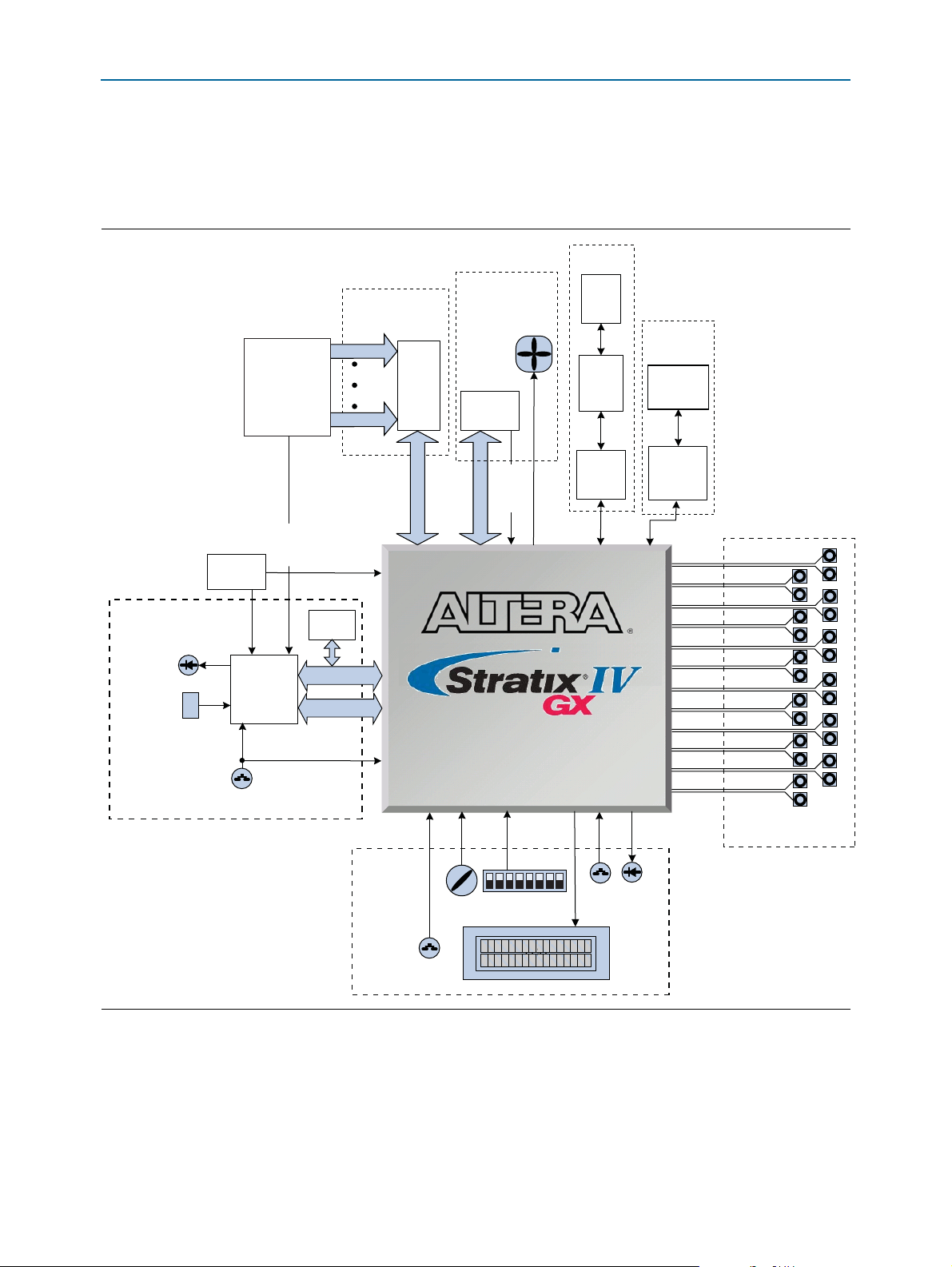
Development Board Block Diagram
Development Board Block Diagram
Figure 1–1 shows the block diagram of the Stratix IV GX transceiver signal integrity
board.
Figure 1–1. Stratix IV GX Transceiver Signal Integrity Board Block Diagram
Transceiver Signal Integrity Development Kit, November 2011 Altera Corporation
Stratix IV GX Edition Reference Manual
Page 9

Chapter 1: Overview 1–5
Handling the Board
Handling the Board
When handling the board, it is important to observe the following static discharge
precaution:
c Without proper anti-static handling, the board can be damaged. Therefore, use anti-
static handling precautions when touching the board.
The Stratix IV GX transceiver signal integrity board must be stored between –40º C
and 100º C. The recommended operating temperature is between 0º C and 55º C.
November 2011 Altera Corporation Transceiver Signal Integrity Development Kit,
Stratix IV GX Edition Reference Manual
Page 10

1–6 Chapter 1: Overview
Handling the Board
Transceiver Signal Integrity Development Kit, November 2011 Altera Corporation
Stratix IV GX Edition Reference Manual
Page 11

Introduction
1 A complete set of schematics, a physical layout database, and GERBER files for the
f For information about powering up the board and installing the development kit
2. Board Components
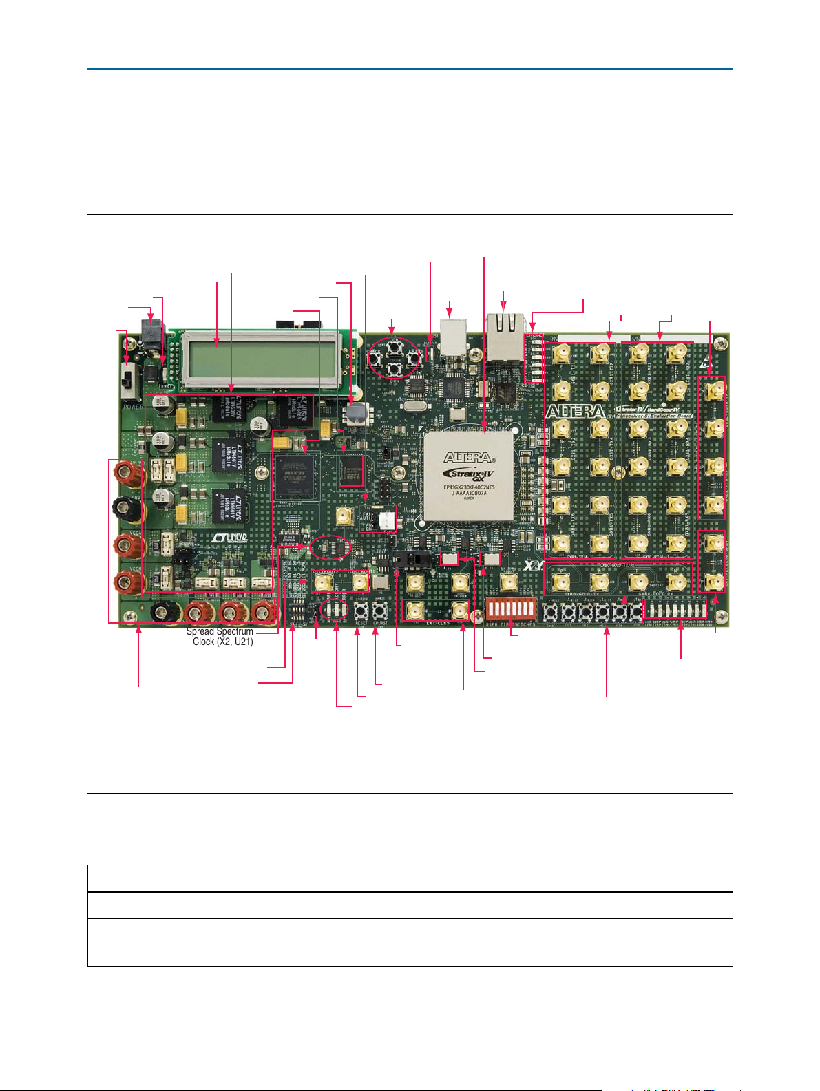
This chapter introduces all the important components on the Stratix IV GX transceiver
signal integrity development board. Figure 2–1 illustrates major component locations
and Table 2–1 lists a brief description of all features of the board.
development board reside in the Stratix IV GX transceiver signal integrity
development kit installation directory.
software, refer to the Transceiver Signal Integrity Development Kit, Stratix IV GX Edition
Getting Started User Guide.
This chapter consists of the following sections:
■ “Board Overview”
■ “Featured Device: Stratix IV GX” on page 2–6
■ “Configuration, Status, and Setup Elements” on page 2–9
■ “General User Input/Output” on page 2–15
■ “Flash Memory Device” on page 2–18
■ “Components and Interfaces” on page 2–20
■ “Power” on page 2–25
November 2011 Altera Corporation Transceiver Signal Integrity Development Kit,
Stratix IV GX Edition Reference Manual
Page 12
2–2 Chapter 2: Board Components
Powe r
Switch
(SW1)
DC Power
Jack (J1)
Power LED (D3)
LCD Display (J24)
Power Circuit (U1-U12)
MAX II CPLD
(U32)
Flash Memory (U39)
Power Select
Switch (SW16)
LCD Directional
Buttons
(SW3-SW6)
Spread Spectrum
Clock (X2, U21)
IO CLK OUT
from FPGA to SMA (J16, J17)
Spread Spectrum
Clock Settings (SW2)
Config
Program
Selection
Jumper
(J62)
User DIP Switches
(SW7)
156.25 MHz Osc (Y5)
External Clock SMA to FPGA
(J14, J15)
100 MHz Osc (Y4)
Socketed
Osc (Y3)
CPU Reset (SW9)
Board Reset (SW8)
Config Status LEDs
(D16-D18)
Fan Connector (J12)
Fan Jumper (J64)
Fan LED (D6)
Embedded
USB-Blaster
Activity LED (D7)
GXB2
TX/RX
SMAs
(J31, J33,
J35, J37)
GXB1
RX SMAs
(J38, J40,
J42, J44,
J46, J48,
J50, J52,
J54, J56,
J58, J60)
GXB1
TX SMAs
(J39, J41,
J43, J45,
J47, J49,
J51, J53,
J55, J57,
J59, J61)
Ethernet
Status
LEDs
(D19-D24)
Embedded
USB-Blaster
(CN1)
Stratix IV GX
FPGA (U33)
10/100 /1000
Ethernet (J68)
User
Push-Buttons
(SW10-SW15)
GXB0
External
SMA
Refclk0
to FPGA
(J19, J20)
User
LEDs
(D8-D15)
External Power
Input Banana
Jacks (J2-J5, J7, J9-J10)
GXB0 TX/RX
SMAs
(J30, J32,
J34, J36)
Board Overview
Board Overview
This section provides an overview of the Stratix IV GX transceiver signal integrity
development board, including an annotated board image and component
descriptions. Figure 2–1 shows an overview of the board features.
Figure 2–1. Overview of the Stratix IV GX Transceiver Signal Integrity Board Features
(1)
Note to Figure 2–1:
(1) The Stratix IV GX Transceiver Signal Integrity board depicted here is the engineering silicon board. For the production silicon board, components
F4, F5, J8, R21, and R23 have been removed and F84 has been added.
Tab le 2– 1 describes the components and lists their corresponding board references.
Table 2–1. Stratix IV GX Transceiver Signal Integrity Development Board Components (Part 1 of 4)
(1)
Board Reference Type Description
Featured Devices
U33 EP4SGX230KF40 Stratix IV GX device in a 1517-pin FBGA package.
Configuration, Status, and Setup Elements
Transceiver Signal Integrity Development Kit, November 2011 Altera Corporation
Stratix IV GX Edition Reference Manual
Page 13
Chapter 2: Board Components 2–3
Board Overview
Table 2–1. Stratix IV GX Transceiver Signal Integrity Development Board Components (Part 2 of 4)
(1)
Board Reference Type Description
J28 JTAG programming header
J26
J63
MAX II JTAG configuration
jumper
JTAG for embedded
USB-Blaster MAX II CPLD
U32 MAX II CPLD
D6 Fan LED
JTAG programming header for connecting an Altera USB-Blaster
dongle to program the FPGA and MAX II CPLD devices.
Jumper to bypass the MAX II CPLD from the JTAG programming
chain.
JTAG for embedded USB-Blaster MAX II CPLD device programming.
Altera EPM1270256C3N, MAX II 256-pin CPLD for MAX II+Flash FPP
configuration.
Indicates an FPGA over-temperature condition exists and a fan should
be attached to the FPGA and running.
D16–D18 Configuration status LEDs LEDs to indicate the status of FPP configuration.
J62
J65
Configuration program select
jumper
Socketed Y3 OSC
enable/disable jumper
Jumper to select the flash configuration image to load upon power-on
or reset.
Jumper to enable or disable the Y3 OSC.
J66 Y4 OSC enable/disable jumper Jumper to enable or disable the Y4 OSC.
J67 Y5 OSC enable/disable jumper Jumper to enable or disable the Y5 OSC.
D3 Power LED Blue LED indicates board power status.
D7 USB-Blaster LED Green activity status LED for embedded USB-Blaster.
D19–D24
J6 VCCA voltage selection jumper This jumper selects the V
J11
SW16
SW2
Bank of Ethernet LINK and
Status LEDs
VCCH voltage selection
jumper
Power measurement rotary
switch
Spread spectrum
configuration DIP switch
Ethernet Link, Speed, Full Duplex, Transmit and Receive activity LEDs.
voltage to the FPGA.
CCA
This jumper selects the V
voltage to the FPGA.
CCH
This switch selects 1 of 6 measured FPGA power rails to display on the
LCD.
DIP switch to set the spread spectrum output clock frequency and
down-spread percentages.
J18 Spread spectrum clock trigger Spread spectrum clock source routed to SMA for triggering purposes.
J21 Y3 OSC clock trigger Y3 oscillator clock source routed to SMA for triggering purposes.
J22 Y4 OSC clock trigger Y4 oscillator clock source routed to SMA for triggering purposes.
J23 Y5 OSC clock trigger Y5 oscillator clock source routed to SMA for triggering purposes.
J14, J15
J19, J20
J16, J17
Differential SMA clock input to
FPGA core
Differential SMA clock input to
FPGA transceiver
Differential SMA clock output
from FPGA core
SMA for receiving a differential external clock input to the FPGA core.
SMA for receiving a differential external clock input to the FPGA
transceiver.
SMA for sending a differential clock output from the FPGA core.
Clock Circuitry
Y2, U20 50-MHz OSC and clock buffer 50-MHz clock to FPGA and MAX II CPLD.
Y3, U22
November 2011 Altera Corporation Transceiver Signal Integrity Development Kit,
Socketed OSC and clock
buffer
5×7-mm oscillator socket for installing alternate oscillator frequencies
to the FPGA transceivers.
Stratix IV GX Edition Reference Manual
Page 14
2–4 Chapter 2: Board Components
Board Overview
Table 2–1. Stratix IV GX Transceiver Signal Integrity Development Board Components (Part 3 of 4)
(1)
Board Reference Type Description
Y4, U23
Y5, U24
100-MHz OSC and clock
buffer
156.25-MHz OSC and clock
buffer
100-MHz clock to FPGA transceivers.
156.25-MHz clock to FPGA transceivers.
X1 6-MHz XTAL XTAL for FTDI USB PHY Device.
Y1 24-MHz OSC 24-MHz oscillator for embedded USB-Blaster MAX II CPLD.
X3 25-MHz OSC 25-MHz oscillator for Marvell 88E1111 Ethernet PHY device.
X2, U21
25-MHz OSC and spread
spectrum clock buffer
25-MHz oscillator and spread spectrum clock buffer circuitry.
General User Input and Output
SW7 Bank of 8 user DIP switches User DIP switches.
SW10–SW15 Bank of 6 user push buttons User push buttons.
D8–D15 Bank of 8 user LEDs User LEDs.
SW3–SW6 LCD control push buttons
J25
General purpose user I/O
header field
Up, Down, Back, and Enter push buttons for implementing user LCD
menu/control.
Four user I/Os brought out to a 0.1 in. header field.
J24 LCD interface header Header for interfacing a 16 character × 2 line LCD.
Memory Devices
U39 Flash memory 512-Mb flash memory.
Components and Interfaces
CN1 USB Type-B connector USB interface for embedded USB-Blaster.
U17 MAX II CPLD
Altera EPM7064AETC44 MAX II CPLD device for embedded
USB-Blaster circuitry.
J68 Ethernet RJ45 jack Halo HFJ11-1G02E RJ45 Ethernet jack with integrated magnetic.
U40 10/100/1000 Ethernet PHY Marvell 88E1111 triple speed Ethernet PHY.
J34, J36 GXB0 transmit channel 0 Transceiver GXB0 transmit channel 0 connected to SMA.
J30, J32 GXB0 receive channel 0 Transceiver GXB0 receive channel 0 connected to SMA.
J39, J41 GXB1 transmit channel 1 Transceiver GXB1 transmit channel 1 connected to SMA.
J43, J45 GXB1 transmit channel 2 Transceiver GXB1 transmit channel 2 connected to SMA.
J55, J57 GXB1 transmit channel 3 Transceiver GXB1 transmit channel 3 connected to SMA.
J59, J61 GXB1 transmit channel 4 Transceiver GXB1 transmit channel 4 connected to SMA.
J47, J49 GXB1 transmit channel 5 Transceiver GXB1 transmit channel 5 connected to SMA.
J51, J53 GXB1 transmit channel 6 Transceiver GXB1 transmit channel 6 connected to SMA.
J38, J40 GXB1 receive channel 1 Transceiver GXB1 receive channel 1 connected to SMA.
J42, J44 GXB1 receive channel 2 Transceiver GXB1 receive channel 2 connected to SMA.
J54, J56 GXB1 receive channel 3 Transceiver GXB1 receive channel 3 connected to SMA.
J58, J60 GXB1 receive channel 4 Transceiver GXB1 receive channel 4 connected to SMA.
J46, J48 GXB1 receive channel 5 Transceiver GXB1 receive channel 5 connected to SMA.
J50, J52 GXB1 receive channel 6 Transceiver GXB1 receive channel 6 connected to SMA.
Transceiver Signal Integrity Development Kit, November 2011 Altera Corporation
Stratix IV GX Edition Reference Manual
Page 15

Chapter 2: Board Components 2–5
Board Overview
Table 2–1. Stratix IV GX Transceiver Signal Integrity Development Board Components (Part 4 of 4)
(1)
Board Reference Type Description
J31, J33 GXB2 transmit channel 7 Transceiver GXB2 transmit channel 7 connected to SMA.
J35, J37 GXB2 receive channel 7 Transceiver GXB2 receive channel 7 connected to SMA.
J12 Fan power connector Power connector for 5-V DC fan sink.
J64 Fan control jumper
Jumper to select whether the fan is always on or automatically
controlled by the FPGA.
SW8 Reset push button Board reset push button.
SW9 CPU reset push button CPU reset push button.
Power
J1 Power Input Jack
14-V – 20-V DC female input power jack. Accepts 2.5-mm male
center-positive barrel from supplied 16-V DC power supply.
SW1 Power switch Switch to power on/off the board.
J2 0.9-V banana jack
Banana jack for supplying external 0.9-V V
F1 and F2 must be removed prior to supplying external power to this
power to the FPGA. Fuses
CC
banana jack.
J3 VCCA banana jack
J7 VCCR and VCCT banana jack
Banana jack for supplying external V
must be removed prior to supplying external power to this banana jack.
Banana jack for supplying external V
Fuse F84 must be removed prior to supplying external power to this
power to the FPGA. Fuse F3
CCA
CCR
and V
power to the FPGA.
CCT
banana jack.
J9 VCCH banana jack
J10 VCCL banana jack
Banana jack for supplying external V
must be removed prior to supplying external power to this banana jack.
Banana jack for supplying external V
must be removed prior to supplying external power to this banana jack.
power to the FPGA. Fuse F6
CCH
power to the FPGA. Fuse F7
CCL
J4, J5 GND banana jack Banana jack connected to GND of the board.
F1, F2 10A fuse
F3 2A fuse
F6 5A fuse
F7 2A fuse
F84 5A fuse
U14 Power measurement ADC
Fuses for 0.9-V V
when an external power is applied to this banana jack.
Fuse for V
CCA
external power is applied to this banana jack.
Fuse for V
CCH
external power is applied to this banana jack.
Fuse for V
CCL
external power is applied to this banana jack.
Fuse for V
CCR
when an external power is applied to this banana jack.
Linear Technology LTC2418CGN 24-bit delta-sigma analog to digital
converter (ADC).
R3 0.001-Ω Rsense Sense resistor for measuring FPGA V
R11 0.009-Ω Rsense Sense resistor for measuring FPGA V
R24 0.009-Ω Rsense Sense resistor for measuring FPGA V
R25 0.009-Ω Rsense Sense resistor for measuring FPGA V
R20 0.009-Ω Rsense Sense resistor for measuring FPGA V
Note to Table 2–1:
(1) Information for the board reference whose components on the engineering silicon board differ from the production silicon board are listed in
Table A–2 on page A–2.
core of the FPGA. These fuses must be removed
CC
power of the FPGA. This fuse must be removed when an
power of the FPGA. This fuse must be removed when an
power of the FPGA. This fuse must be removed when an
and V
power of the FPGA. This fuse must be removed
CCT
core power.
CC
power.
CCA
power.
CCH
power.
CCL
CCR
and V
combined power.
CCT
November 2011 Altera Corporation Transceiver Signal Integrity Development Kit,
Stratix IV GX Edition Reference Manual
Page 16

2–6 Chapter 2: Board Components
Bank 8A 40
Bank 8B 24
Bank 8C 32
Bank 7C 32
Bank 6A 48
Bank 6C
EP4SGX230
Bank
Name
Number
of I/Os
40
Bank 5C 40
Bank 5A
Bank 1A
Bank 1C
Bank 2C
Bank 2A 48
48
40
40
48
Bank 7B 24
Bank 7A 40
Bank
Name
Number
of I/Os
Bank 3A40
Bank 3B24
Bank 3C32
Bank 4C32
Bank 4B24
Bank 4A40
4*
4*
Bank
GXBL2
4*
Bank
GXBL1
Bank
GXBL0
4*
4*
4*
Bank
GXBR2
Bank
GXBR1
Bank
GXBR0
*Number of
Transceiver
Channel
Featured Device: Stratix IV GX
Featured Device: Stratix IV GX
The Stratix IV GX transceiver signal integrity development board features the
EP4SGX230KF40 Stratix IV FPGA device (U33) in a 1517-pin FBGA package.
f For more information about Stratix IV GX devices, refer to the Stratix IV Device
Handbook.
Tab le 2– 2 describes the features of the Stratix IV GX EP4SGX230KF40 device.
Table 2–2. Stratix IV GX Device EP4SGX230KF40 Features
ALMs
Equivalent
LEs
M9K
RAM
Blocks
M144K
Blocks
Total
RAM
bits
DSP
Blocks
18-bit × 18-bit
Multipliers
PLLs
Maximum
User I/O pins
91,200 228,000 1,235 22 17,133 161 1,288 8 736
Tab le 2– 3 lists the Stratix IV GX component reference and manufacturing
information.
Table 2–3. Stratix IV GX Device Component Reference and Manufacturing Information
Board Reference Description Manufacturer
U33 Stratix IV GX Altera
Corporation EP4SGX230KF40 www.altera.com
Manufacturing
Part Number
I/O Resources
Figure 2–2 shows the bank organization and I/O count for the EP4SGX230K device in
a 1517-pin FBGA package.
Figure 2–2. Stratix IV GX Device I/O Bank Diagram
Package
Type
1517-pin
FBGA
Manufacturer
Website
Transceiver Signal Integrity Development Kit, November 2011 Altera Corporation
Stratix IV GX Edition Reference Manual
Page 17

Chapter 2: Board Components 2–7
Featured Device: Stratix IV GX
Tab le 2– 4 summarizes the FPGA I/O usage by function on the Stratix IV GX
transceiver signal integrity development board. I/O direction is with respect to the
FPGA.
Table 2–4. Stratix IV GX I/O Usage Summary (Part 1 of 3)
Function I/O Type I/O Count Description
FPGA Transceiver Clocks
100-MHz Diff Clock LVDS input 2 Diff REFCLK Input
Socketed Diff Clock LVDS input 2 Diff REFCLK Input
156.25-MHz Diff Clock LVDS input 2 Diff REFCLK Input
SMA Diff Clock Inputs LVDS input 2 Diff REFCLK Input
FPGA Global Clocks
50-MHz Clock 2.5-V CMOS input 1 Global Clock Input
Spread Spectrum Clock LVDS input 2 Diff Global Clock
SMA Diff Clock Input LVDS input 2 Diff Global Clock
SMA Diff I/O or Clock Output — 2 Diff Global I/O or Clock Output
Temperature Monitor
Temp Sense Diodes Analog 2 Stratix IV GX Internal Sense Diode
Power Measure
ADC Interface 2.5-V CMOS 5 8 Diff Channel 24-bit A/D Converter
Temp Measure
MAX1619 Interface 2.5V CMOS 4 Die Temp Sense
EEPROM
EEP_CSn 2.5--V CMOS output 1 EEPROM Chip Select
Fan
FAN_On 2.5-V CMOS output 1 Fan Control
FAN_LED 2.5-V CMOS output 1 Fan LED
USB-Blaster
JTAG USB-Blaster or JTAG
header
2.5-V CMOS 4
Built-in USB-Blaster or
JTAG 0.1-mm header for Debug
FPP Configuration
FPGA Dclk 2.5-V CMOS input 1 FPP Dclk
FPGA D[7:0] 2.5-V CMOS input 8 FPP Data
MSEL [2:0] 2.5-V CMOS input 3 Dedicated Configuration Pins
NCONFIG 2.5-V CMOS input 1 Dedicated Configuration Pins
NSTATUS 2.5-V CMOS inout 1 Dedicated Configuration Pins
NCE 2.5-V CMOS input 1 Dedicated Configuration Pins
CONFIG_DONE 2.5-V CMOS inout 1 Dedicated Configuration Pins
INIT_DONE 2.5-V CMOS output 1 Dedicated Configuration Pins
PGM[2:0] 2.5-V CMOS output 3 Configuration Program Select Pins
November 2011 Altera Corporation Transceiver Signal Integrity Development Kit,
Stratix IV GX Edition Reference Manual
Page 18

2–8 Chapter 2: Board Components
Featured Device: Stratix IV GX
Table 2–4. Stratix IV GX I/O Usage Summary (Part 2 of 3)
Function I/O Type I/O Count Description
Flash Memory
ADDR[25:0] 2.5-V CMOS output 26 Flash Address Bus
DATA[15:0] 2.5-V CMOS inout 16 Flash Data Bus
FLASH_CEn 2.5-V CMOS output 1 Flash Chip Enable
FLASH_OEn 2.5-V CMOS output 1 Flash Read Strobe
FLASH_WEn 2.5-V CMOS output 1 Flash Write Strobe
FLASH_BSYn 2.5-V CMOS input 1 Flash Busy
FLASH_CLK 2.5-V CMOS output 1 Flash Clock
FLASH_RSTn 2.5-V CMOS output 1 Flash Reset
FLASH_ADVn 2.5-V CMOS output 1 Flash Address Valid
FLASH_WPn 2.5-V CMOS output 1 Flash Write Protect
Resets
CPU_RESETn 2.5-V CMOS input 1 Nios
®
II CPU Reset
S4GX_RESETn 2.5-V CMOS input 1 S4GX General FPGA Reset
Switches, Buttons, LEDS
User Push Buttons 2.5-V CMOS input 6 6 User Push Buttons
User DIP Switches 2.5-V CMOS input 8 8 User DIP Switches
User LEDS 2.5-V CMOS output 8 8 User LEDs (GREEN)
HEX Rotary Switch 2.5-V CMOS input 4 16 Position Rotary Switch
Directional Menu Buttons 2.5-V CMOS input 4 4 LCD Menu Buttons
User I/Os 2.5-V CMOS inout 4 4 User I/O pins to header field
LCD
16 Character × 2 Line LCD 2.5-V CMOS 11 LCD
Ethernet
TXD[3:0] 2.5-V CMOS output 4 Ethernet Transmit RGMII Data Bus
TXEN 2.5-V CMOS output 1 Ethernet Transmit Enable
GTXCLK 2.5-V CMOS output 1 Ethernet Transmit Clock
RXD[3:0] 2.5-V CMOS input 4 Ethernet Receive RGMII Data Bus
RXDV 2.5-V CMOS input 1 Receive Data Valid
RXCLK 2.5-V CMOS input 1 Receive Clock
MDC 2.5-V CMOS input 1 Ethernet MII Clock
MDIO 2.5-V CMOS inout 1 Ethernet MII Data
ENET_SGMII_TXP/N LVDS output 2 Ethernet SGMII Transmit Data Positive/Negative
ENET_SGMII_RXP/N LVDS input 2 Ethernet SGMII Receive Data Positive/Negative
Transceivers
GXB0 Transmit Channel Transceiver channel 2 Minimize Trace Length (2.5 in.)
GXB0 Receive Channel Transceiver channel 2 Minimize Trace Length (2.5 in.)
GXB2 Long Transmit Channel Transceiver channel 2 33 in. Trace Length (8.5G)
Transceiver Signal Integrity Development Kit, November 2011 Altera Corporation
Stratix IV GX Edition Reference Manual
Page 19

Chapter 2: Board Components 2–9
Configuration, Status, and Setup Elements
Table 2–4. Stratix IV GX I/O Usage Summary (Part 3 of 3)
Function I/O Type I/O Count Description
GXB2 Short Receive Channel Transceiver channel 2 7 in. Trace Length (8.5G)
GXB1 6 Full Duplex
Transceiver Channels
(One entire block)
Spares
Spare[7:0] 2.5-V CMOS inout 8 Spare signals to the MAX II CPLD
Total Device I/O: 208
Available Stratix IV GX I/O: 736
Transceiver channel 24
Four Full Duplex channels from one entire
transceiver block (two from clock multiplier unit
(CMU) block)
Configuration, Status, and Setup Elements
This section describes the board’s configuration, status, and setup elements.
Configuration
The Stratix IV GX transceiver signal integrity development board supports three
configuration methods:
■ Embedded USB-Blaster is the default method for configuring the FPGA at any
time using the Quartus II Programmer in JTAG mode with the supplied USB cable.
■ MAX II+Flash FPP download for configuring the FPGA using stored images from
the flash on either power-up or pressing the reset push button (SW8).
■ JTAG programming header (J28) for configuring the FPGA using an external
USB-Blaster (not supplied) and the Quartus II Programmer.
The following sections describe each of these methods.
Embedded USB-Blaster
Figure 2–3 shows the block diagram for the embedded USB-Blaster. The USB-Blaster
is implemented using a Type-B USB connector (CN1), a Future Technologies FT245BL
USB PHY device (U16), and an Altera MAX7064 CPLD (U17). This allows
configuration of the FPGA using a USB cable directly connected between the USB port
on the board (CN1) and a USB port of a PC running the Quartus II software.
November 2011 Altera Corporation Transceiver Signal Integrity Development Kit,
Stratix IV GX Edition Reference Manual
Page 20

2–10 Chapter 2: Board Components
Configuration, Status, and Setup Elements
A green USB-Blaster LED (D7) indicates the USB-Blaster activity. The embedded
USB-Blaster is automatically disabled when an external USB-Blaster is connected to
the JTAG chain at header J28.
Figure 2–3. Embedded USB-Blaster
JTAG
Header
USB Type-B
Connector
USB
USB 2.0
PHY
USB FIFO Bus
MAX II
CPLD
JTAG
JTAG
Stratix V GX
FPGA
Fast Passive Parallel Download
Figure 2–4 shows the block diagram for the MAX II+Flash FPP configuration. This
method is used for automatic configuration of the FPGA with the configuration
programming image stored in the flash memory. The FPP download controller is
implemented within an Altera MAX II EPM1270F256C3N CPLD (U32). This
controller, together with the Numonyx PC28F512P30BF 512-Mb CFI NOR-type flash
device (U39), performs FPP configuration upon board power-up or reset. The CPLD
shares the flash interface with the FPGA. The configuration program select jumper,
PGMSEL (J62) selects between two Programmer Object Files (.pof)—factory .pof or
user .pof files stored in the flash. The FPP controller uses the Altera Parallel Flash
Loader (PFL) megafunction to configure the FPGA by reading data from the flash and
converting it to FPP format. This data is written to the FPGA’s dedicated
configuration pins during configuration. The configuration mode select signals,
MSEL[2:0]
green configuration status LEDs (D16–D18) indicate the status of the FPP
configuration.
Figure 2–4. MAX II+Flash FPP Configuration
, are pulled to
[0,0,0]
on the board for FPP mode configuration. Three
FPP
(D18)
Configuration
(D16)
ERROR LED
Flash
Flash
Flash
(U39)
Stratix IV GX
FPGA
(U33)
RESET button
(SW8)
PGMSEL
Jumper (J62)
Transceiver Signal Integrity Development Kit, November 2011 Altera Corporation
Stratix IV GX Edition Reference Manual
MAX II CPLD
(U32)
(D17)
USER LED
FACTORY LED
Page 21

Chapter 2: Board Components 2–11
J28
U33
Stratix IV GX
Stratix IV GX
and MAX II
External
USB-Blaster
Header
Remove jumper to
remove MAX_FPP device
from JTAG header
J26
TDI
TMS
TCK
LAST_TDO
S4GX_TDI
S4GX_TDO
JTAG_TMS
JTAG_TCK
JTAG_TMS
JTAG_TCK
MAX_FPP_TDI
MAX_FPP_TDO
U32
MAX II CPLD
9
5
1
3
Configuration, Status, and Setup Elements
JTAG Programming Header
Figure 2–5 shows the schematic connections for the dedicated JTAG programming
header (J28). This header provides another method for configuring the FPGA (U33)
using an Altera USB-Blaster with the Quartus II Programmer running on a PC. The
MAX II JTAG configuration jumper (J26) allows the MAX II CPLD device to be
removed from the JTAG chain so that the FPGA is the only device on the JTAG chain.
Figure 2–5. JTAG Programming Header
Status and Setup Elements
The development board includes board-specific status LEDs, jumpers, and switches
for enabling and configuring various features on the board, as well as a
16 character × 2 line LCD for displaying board power and temperature
measurements. This section describes the status and setup elements.
Status LEDs
Tab le 2– 5 lists the LED board references, names, and functional descriptions.
Table 2–5. Board-Specific LEDs (Part 1 of 2)
Board
Reference
D3 POWER
D6 FAN
D7 BLASTER Green LED. Blinks to indicate the embedded USB-Blaster activity.
D16 ERROR Red LED. Illuminates when a configuration error has occurred.
D17 FACTORY
D18 USER
D19 TX Green LED. Blinks to indicate Ethernet transmit activity.
D20 RX Green LED. Blinks to indicate Ethernet receive activity.
November 2011 Altera Corporation Transceiver Signal Integrity Development Kit,
LED Name Description
Blue LED. Illuminates when board power switch (SW1) is on.
(Requires 14–20 V input to DC input jack J1)
Amber LED. Illuminates to indicate an FPGA over-temperature condition. A fan sink
must be attached to the FPGA and running to prevent overheating.
Green LED. Illuminates when the factory POF image is successfully programmed into
the FPGA.
Green LED. Illuminates when the user POF image is successfully programmed into the
FPGA.
Stratix IV GX Edition Reference Manual
Page 22

2–12 Chapter 2: Board Components
Configuration, Status, and Setup Elements
Table 2–5. Board-Specific LEDs (Part 2 of 2)
Board
Reference
LED Name Description
D21 DUPLEX Green LED. Illuminates to indicate Ethernet full duplex status.
D22 1000 Green LED. Illuminates to indicate Ethernet linked at 1000 Mbps.
D23 100 Green LED. Illuminates to indicate Ethernet linked at 100 Mbps.
D24 10 Green LED. Illuminates to indicate Ethernet linked at 10 Mbps.
Tab le 2– 6 lists the surface mount LEDs which indicate the various status of the board.
Table 2–6. Status LEDs
Board
Reference
Description
D3 Power LED
D17 FACTORY LED
D18 USER LED
D16 ERROR LED
D19 Ethernet transmit activity LED
D20 Ethernet receive activity LED
D21 Ethernet Full-Duplex LED
D22 Ethernet 1000-Mbyte Link LED
D23 Ethernet 100-Mbyte Link LED
D24 Ethernet 100-Mbyte Link LED
D6 Over-Temperature LED
D7 USB-Blaster activity LED
Schematic
Signal Name
5V
FACTORY_IMAGE
USER_IMAGE
CONFIG_ERR
ENET_LED_TX
ENET_LED_RX
ENET_LED_DUPLEX
ENET_LED_LINK1000
ENET_LED_LINK100
ENET_LED_LINK10
FAN_LED
USB_LED
I/O Standard
———
2.5-V CMOS — U32 pin R8
2.5-V CMOS — U32 pin R7
2.5-V CMOS — U32 pin R9
2.5-V CMOS — U40 pin 68
2.5-V CMOS — U40 pin 69
2.5-V CMOS — U40 pin 70
2.5-V CMOS — U40 pin 73
2.5-V CMOS — U40 pin 74
2.5-V CMOS — U40 pin 76
2.5-V CMOS U33 pin F14 —
3.3-V CMOS — U17 pin 8
Stratix IV GX
Pin Number
Device
Other
Connections
Board Jumpers
Tab le 2– 7 lists the board jumper references, names, and functional descriptions.
Table 2–7. Board Jumpers (Part 1 of 2)
Board
Reference
J6 VCCA_SEL
J11 VCCH_SEL
J26
J62 PGMSEL
Transceiver Signal Integrity Development Kit, November 2011 Altera Corporation
Stratix IV GX Edition Reference Manual
Jumper Name Description
VCCA
When a jumper is installed on pins 1-2,
When a jumper is installed on pins 2-3,
When a jumper is installed on pins 1-2,
When a jumper is installed on pins 2-3,
is set to 2.5 V.
VCCA
is set to 3.0 V
VCCH
is set to 1.4 V.
VCCH
is set to 1.5 V
When a jumper is installed, the MAX II CPLD device (U32) is included in the JTAG
MAXII
BYPASS
programming chain.
When a jumper is removed, the MAX II CPLD device (U32) is removed from the JTAG
programming chain.
When a jumper is installed on pins 1-2, FPP configuration loads the user POF image
from flash.
When a jumper is installed on pins 2-3, FPP configuration loads the factory POF image
from flash.
Page 23

Chapter 2: Board Components 2–13
Configuration, Status, and Setup Elements
Table 2–7. Board Jumpers (Part 2 of 2)
Board
Reference
J64 FAN
J65
J66
J67
Jumper Name Description
When a jumper is installed on pins 1-2, the fan is automatically controlled by the FPGA.
When a jumper is installed on pins 2-3, the fan is always on.
Y3 OSC
EN/DIS
Y4 OSC
EN/DIS
Y5 OSC
EN/DIS
When a jumper is installed, Y3 oscillator is disabled.
When a jumper is removed, Y3 oscillator is enabled and running.
When a jumper is installed, Y4 oscillator is disabled.
When a jumper is removed, Y4 oscillator is enabled and running.
When a jumper is installed, Y5 oscillator is disabled.
When a jumper is removed, Y5 oscillator is enabled and running.
There is a mini-DIP switch (SW2) for configuring the spread spectrum clock device
(U21). Ta bl e 2 –8 lists the connection of the mini-DIP switch (SW2).
Table 2–8. Mini-DIP Switch Pin-Out (SW2)
Board
Reference
Description
SW2 pin 1 (S0) Spread spectrum clock
SW2 pin 2 (S1)
SW2 pin 3 (S2)
configuration DIP switch.
When the switch is in the
open position, a logic 1 is
selected. When the switch is
SW2 pin 4 (S3)
in the closed position, a logic
0 is selected.
Schematic
Signal Name
S0
S1
SS0
SS1
I/O Standard
Stratix IV GX
Device
Pin Name
Other
Connections
2.5-V CMOS — U21 pin 1
2.5-V CMOS — U21 pin 2
2.5-V CMOS — U21 pin 3
2.5-V CMOS — U21 pin 8
Tab le 2– 9 summarizes the mini-DIP switch (SW2) functionality.
Table 2–9. Mini-DIP Switch Configuration (SW2)
S1 S0 Clock Frequency S3 S2 Spread Spectrum %
0 0 25 MHz 0 0 Center ±25
0 1 100 MHz 0 1 Down –0.50
1 0 125 MHz 1 0 Down –0.75
1 1 200 MHz 1 1 No spread spectrum
November 2011 Altera Corporation Transceiver Signal Integrity Development Kit,
Stratix IV GX Edition Reference Manual
Page 24

2–14 Chapter 2: Board Components
50-MHz
OSC (Y2)
ICS8304
CLKBUF
(U20)
MAX II CPLD
(U32)
CLKIN SMA
(J14, J15)
Trigger
SMA (J18)
Trigger
SMA (J21)
25-MHz
XTAL (Y2)
Trigger
SMA (J22)
Trigger
SMA (J23)
CLKIN SMA
(J19, J20)
ICS557
Spread
Spectrum
CLKBUF
(U21)
DIPSW
(SW2)
Stratix IV GX
FPGA
(U33)
CLKOUT SMA
(J16, J17)
OSC
Socket
(Y3)
ICS8543
CLKBUF
(U22)
EN JMP
(J66)
100 MHz
OSC
(Y4)
ICS85411
CLKBUF
(U23)
ICS85411
CLKBUF
(U24)
EN JMP
(J67)
156.25 OSC
(Y5)
EN JMP
(J65)
Clocks
Clocks
Clocking for the Stratix IV GX transceiver signal integrity board is provided
separately for both the FPGA core and transceivers. The core clocks include a
dedicated 50-MHz clock, a spread spectrum clock capable of producing either
25-MHz, 100-MHz, 125-MHz, or 200-MHz clock, and a pair of SMA connectors to
receive a differential external clock. The dedicated transceiver clocks include a
100-MHz, 156.25-MHz clock source, and a socket for accepting a 5×7-mm 6-pin
oscillator. This socket has the flexibility of providing any custom oscillator frequency
to the transceivers. Additionally, if an oscillator with the desired frequency is not
readily available, the transceivers can receive a differential clock from an external
source through a pair of SMA connectors.
Figure 2–6 shows the Stratix IV GX transceiver signal integrity development board
clocking diagram.
Figure 2–6. Stratix IV GX Transceiver Signal Integrity Board Clocking Diagram
Transceiver Signal Integrity Development Kit, November 2011 Altera Corporation
Stratix IV GX Edition Reference Manual
Page 25

Chapter 2: Board Components 2–15
General User Input/Output
Tab le 2– 10 lists the clock distribution for the Stratix IV GX transceiver signal integrity
development board.
Table 2–10. Stratix IV GX Transceiver Signal Integrity Board Clock Distribution
Frequency Signal Name Signal Originates From
50 MHz
User Input
User Defined
User Defined
25 MHz, 100 MHz, 125 MHz, 200 MHz
(Y2)
(Frequencies set by switch SW2)
User Input
OSC Socket
(Y3)
156.25 MHz
(Y5)
100 MHz
(Y4)
25 MHz, 100 MHz, 125 MHz, 200 MHz
Socket
(Y3)
100 MHz
(Y4)
156.25 MHz
(Y5)
MAXII_50M_CLK
S4GX_50M_CLK4P
S4GX_EXT_CLK5P
S4GX_EXT_CLK5N
IO_CLKOUT1
IO_CLKOUT2
S4GX_CLK1P
S4GX_CLK1N
EXT_REFCLK0P_GXB0
EXT_REFCLK0N_GXB0
SKT_REFCLK1P_GXB0
155.52M_REFCLK1N_GXB0
156.25M_REFCLK1P_GXB2
156.25M_REFCLK1N_GXB2
100M_REFCLK0P_GXB2
100M_REFCLK0N_GXB2
X2 Trigger
Y3 Trigger
Y4 Trigger
Y5 Trigger
Signal
Propagates To
U20 pin 8
U20 pin 7
SMA J14
SMA J15
U33 pin M20 SMA J16
U33 pin L20 SMA J17
U21 pin 15
U21 pin 14
SMA J19
SMA J20
U22 pin 20
U22 pin 19
U24 pin 1
U24 pin 2
U23 pin 1
U23 pin 2
U21 pin 11 SMA J18
U22 pin 12 SMA J21
U23 pin 3 SMA J22
U24 pin 3 SMA J23
U32 pin H5
U33 pin AR22
U33 pin AV22
U33 pin AW22
U33 pin AB34
U33 pin AA35
U33 pin AN38
U33 pin AN39
U33 pin AL38
U33 pin AL39
U33 pin G38
U33 pin G39
U33 pin J38
U33 pin J39
General User Input/Output
This section describes the user I/O interface to the FPGA including the push buttons,
user and status LEDs, LCD, and user DIP, rotary, and slide switches. Table 2–11 lists
the component references and the manufacturing information.
Table 2–11. Component Reference Input and Ouput Devices (Part 1 of 2)
Board Reference
SW3–SW6,
SW8–SW15
D7–D15,
D17–D24
November 2011 Altera Corporation Transceiver Signal Integrity Development Kit,
Device
Description
Push Buttons Panasonic Corporation EVQPAC07K www.panasonic.com
Green LEDs Lumex Inc. SML-LX1206GC-TR www.lumex.com
Manufacturer
Manufacturer
Part Number
Stratix IV GX Edition Reference Manual
Manufacturer
Website
Page 26

2–16 Chapter 2: Board Components
General User Input/Output
Table 2–11. Component Reference Input and Ouput Devices (Part 2 of 2)
Board Reference
Device
Description
Manufacturer
Manufacturer
Part Number
Manufacturer
Website
D16 Red LED Lumex Inc. SML-LX1206IC-TR www.lumex.com
D6 Amber LED Lite-on Technology Corporation LTST-C150KYKT www.liteon.com
D3 Blue LED Lumex Inc. SML-LX1206USBC-TR www.lumex.com
LCD LCD Lumex Inc. LCM-S01602DSR/C www.lumex.com
SW7 DIP switch Grayhill Corporation 76SB08ST www.grayhill.com
SW2 Mini-DIP switch
C&K Components /
ITT Industries
TDA04H0SB1 www.ittcannon.com
SW16 Rotary switch Grayhill Corporation 94HCB16WT www.grayhill.com
SW1 Slide switch E-switch Inc. EG2201A www.e-switch.com
Push Buttons
The board has 12 push buttons for user-defined logic input. Each push-button drives
logic low when pressed and returns to driving logic high when released. Tab le 2– 12
summarizes these push buttons.
Table 2–12. Push Buttons Signal Names and Functions
Board
Reference
SW10
SW11
SW12
SW13
SW14
SW15
SW8
SW9
SW3
SW4
SW5
SW6
Description
General purpose user push-button
switches. These switches are not
debounced.
Board reset. These switches are
not debounced.
CPU reset. These switches are not
debounced.
LCD menu directional
push-buttons switches. These
switches are not debounced.
Schematic
Signal Name
USR_PB0
USR_PB1
USR_PB2
USR_PB3
USR_PB4
USR_PB5
RESETn
CPURSTn
BACK
ENTR
UP
DWN
I/O Standard
2.5-V CMOS U33 pin AW28
2.5-V CMOS U33 pin AV28
2.5-V CMOS U33 pin AU28
2.5-V CMOS U33 pin AT28
2.5-V CMOS U33 pin AR28
2.5-V CMOS U33 pin AP28
2.5-V CMOS — U32 pin T2
2.5-V CMOS U33 pin AW18
2.5-V CMOS U33 pin G21
2.5-V CMOS U33 pin G23
2.5-V CMOS U33 pin G22
2.5-V CMOS U33 pin H22
Stratix IV GX
Device
Pin Number
Other
Connections
10-kΩ pull-up
resistor to 2.5 V
10-kΩ pull-up
resistor to 2.5 V
10-kΩ pull-up
resistor to 2.5 V
Transceiver Signal Integrity Development Kit, November 2011 Altera Corporation
Stratix IV GX Edition Reference Manual
Page 27

Chapter 2: Board Components 2–17
General User Input/Output
User LEDs
A bank of eight green, surface mount LEDs (SM1206 type) are provided for general
purpose use. The cathodes of these LEDs are each connected to an FPGA I/O pin
while the anodes are pulled to 2.5 V through a current limiting resistor. Driving the
corresponding FPGA I/O pin low illuminates the LED. Driving the pin high turns the
LED off. Table 2–13 lists the assignment for each user LED.
Table 2–13. User LED Pin-Out (Green)
Board
Reference
D8
D9
D10
D11
D12
D13
D14
D15
General purpose green
surface mount (type 1206)
user LEDs.
Driving a logic 0 on the I/O
port turns the LED ON.
Driving a logic 1 on the I/O
port turns the LED OFF.
Description
LCD
The develpment board includes a 16 character × 2 line LCD which connects directly to
the FPGA device. Table 2–14 lists the LCD pin assignments.
Table 2–14. Seven-Segment Display Pin-Out
Board Reference Description
LCD LCD DATA 0
LCD LCD DATA 1
LCD LCD DATA 2
LCD LCD DATA 3
LCD LCD DATA 4
LCD LCD DATA 5
LCD LCD DATA 6
LCD LCD DATA 7
LCD LCD ENABLE Signal
LCD LCD DATA/CONTROL Signal
LCD LCD Write Enable Strobe
Schematic
Signal Name
USR_LED0
USR_LED1
USR_LED2
USR_LED3
USR_LED4
USR_LED5
USR_LED6
USR_LED7
Schematic
Signal Name
LCD_DATA0
LCD_DATA1
LCD_DATA2
LCD_DATA3
LCD_DATA4
LCD_DATA5
LCD_DATA6
LCD_DATA7
LCD_EN
LCD_D_Cn
LCD_Wen
I/O Standard
2.5-V CMOS
I/O Standard
2.5-V CMOS
Stratix IV GX
Device
Pin Number
U33 pin AW29 160 Ω to 2.5 V
U33 pin AV29 160 Ω to 2.5 V
U33 pin AU29 160 Ω to 2.5 V
U33 pin AT29 160 Ω to 2.5 V
U33 pin AW30 160 Ω to 2.5 V
U33 pin AT30 160 Ω to 2.5 V
U33 pin AP30 160 Ω to 2.5 V
U33 pin AN30 160 Ω to 2.5 V
Stratix IV GX
Device
Pin Name
U33 pin B17 J24 pin 7
U33 pin B19 J24 pin 8
U33 pin D21 J24 pin 9
U33 pin D22 J24 pin 10
U33 pin D23 J24 pin 11
U33 pin E22 J24 pin 12
U33 pin E23 J24 pin 13
U33 pin F23 J24 pin 14
U33 pin C22 J24 pin 6
U33 pin A18 J24 pin 4
U33 pin A17 J24 pin 5
Other
Connections
Other
Connections
November 2011 Altera Corporation Transceiver Signal Integrity Development Kit,
Stratix IV GX Edition Reference Manual
Page 28

2–18 Chapter 2: Board Components
Flash Memory Device
DIP Switch
The user DIP switch is for reference design functions and general purpose use. This
switch connects to the FPGA device I/O pins. Table 2–15 summarizes the function
and connections of the user DIP switch (SW7).
Table 2–15. User DIP Switch Pin-Out (SW7)
Board Reference Description
SW7 pin 1
SW7 pin 2
SW7 pin 3
SW7 pin 4
SW7 pin 5
SW7 pin 6
SW7 pin 7
SW7 pin 8
User DIP switch
connected to the FPGA
device. When the switch
is in the open position, a
logic 1 is selected.
When the switch is in the
closed position, a logic 0
is selected.
Flash Memory Device
The board features a Numonyx PC28F512P30BF 512-Mb CFI-compliant NOR-type
flash memory device. This device stores configuration files for the FPGA. Both the
MAX II CPLD (U32) and FPGA (U33) devices can access the flash. The MAX II CPLD
access the flash for FPP configuration of the FPGA using the PFL Megafunction. The
FPGA access the flash’s user space for embedded NIOS applications. Table 2–16 lists
the pin-out information of the flash memory interface to the FPGA. The signal
direction is with respect to the FPGA device.
Schematic
Signal Name
USR_DIP0
USR_DIP1
USR_DIP2
USR_DIP3
USR_DIP4
USR_DIP5
USR_DIP6
USR_DIP7
I/O Standard
2.5-V CMOS
Stratix IV GX
Device
Pin Name
U33 pin AW27
U33 pin AU27
U33 pin AT27
U33 pin AP27
U33 pin AN27
U33 pin AP26
U33 pin AN26
U33 pin AM26
Other
Connections
10-kΩ pull-up
resistor to 2.5 V
Table 2–16. Flash Memory Pin-Out (U39) (Part 1 of 2)
Board
Reference
U39 pin A1 Flash Address bus bit 1
U39 pin B1 Flash Address bus bit 2
U39 pin C1 Flash Address bus bit 3
U39 pin D1 Flash Address bus bit 4
U39 pin D2 Flash Address bus bit 5
U39 pin A2 Flash Address bus bit 6
U39 pin C2 Flash Address bus bit 7
U39 pin A3 Flash Address bus bit 8
U39 pin B3 Flash Address bus bit 9
U39 pin C3 Flash Address bus bit 10
U39 pin D3 Flash Address bus bit 11
U39 pin C4 Flash Address bus bit 12
U39 pin A5 Flash Address bus bit 13
Transceiver Signal Integrity Development Kit, November 2011 Altera Corporation
Stratix IV GX Edition Reference Manual
Description
Schematic
Signal Name
F_AD1
F_AD2
F_AD3
F_AD4
F_AD5
F_AD6
F_AD7
F_AD8
F_AD9
F_AD10
F_AD11
F_AD12
F_AD13
I/O Standard
2.5-V CMOS U33 pin AN15 U32 pin M16
2.5-V CMOS U33 pin AM14 U32 pin M15
2.5-V CMOS U33 pin AN14 U32 pin M14
2.5-V CMOS U33 pin AP15 U32 pin N16
2.5-V CMOS U33 pin AP14 U32 pin N15
2.5-V CMOS U33 pin AL15 U32 pin J16
2.5-V CMOS U33 pin AP13 U32 pin N13
2.5-V CMOS U33 pin AN13 U32 pin N14
2.5-V CMOS U33 pin J15 U32 pin C14
2.5-V CMOS U33 pin H13 U32 pin B12
2.5-V CMOS U33 pin M13 U32 pin F15
2.5-V CMOS U33 pin M14 U32 pin F16
2.5-V CMOS U33 pin K15 U32 pin D16
Stratix IV GX
Device
Pin Name
Other
Connections
Page 29

Chapter 2: Board Components 2–19
Flash Memory Device
Table 2–16. Flash Memory Pin-Out (U39) (Part 2 of 2)
Board
Reference
Description
U39 pin B5 Flash Address bus bit 14
U39 pin C5 Flash Address bus bit 15
U39 pin D7 Flash Address bus bit 16
U39 pin D8 Flash Address bus bit 17
U39 pin A7 Flash Address bus bit 18
U39 pin B7 Flash Address bus bit 19
U39 pin C7 Flash Address bus bit 20
U39 pin C8 Flash Address bus bit 21
U39 pin A8 Flash Address bus bit 22
U39 pin G1 Flash Address bus bit 23
U39 pin H8 Flash Address bus bit 24
U39 pin B6 Flash Address bus bit 25
U39 pin F2 Flash Data bus bit 0
U39 pin E2 Flash Data bus bit 1
U39 pin G3 Flash Data bus bit 2
U39 pin E4 Flash Data bus bit 3
U39 pin E5 Flash Data bus bit 4
U39 pin G5 Flash Data bus bit 5
U39 pin G6 Flash Data bus bit 6
U39 pin H7 Flash Data bus bit 7
U39 pin E1 Flash Data bus bit 8
U39 pin E3 Flash Data bus bit 9
U39 pin F3 Flash Data bus bit 10
U39 pin F4 Flash Data bus bit 11
U39 pin F5 Flash Data bus bit 12
U39 pin H5 Flash Data bus bit 13
U39 pin G7 Flash Data bus bit 14
U39 pin E7 Flash Data bus bit 15
U39 pin E6 Flash Clock
U39 pin D4 Flash Reset
U39 pin B4 Flash Chip Enable
U39 pin F8 Flash Output Enable
U39 pin G8 Flash Write Enable
U39 pin F6 Flash Adress Valid
U39 pin C6 Flash Write Protect
U39 pin F7 Flash Busy
Schematic
Signal Name
F_AD14
F_AD15
F_AD16
F_AD17
F_AD18
F_AD19
F_AD20
F_AD21
F_AD22
F_AD23
F_AD24
F_AD25
F_D0
F_D1
F_D2
F_D3
F_D4
F_D5
F_D6
F_D7
F_D8
F_D9
F_D10
F_D11
F_D12
F_D13
F_D14
F_D15
F_CLK
F_RSTn
F_CEn
F_OEn
F_Wen
F_ADVn
F_WPn
F_BSYn
I/O Standard
Stratix IV GX
Device
Pin Name
Other
Connections
2.5-V CMOS U33 pin G13 U32 pin A11
2.5-V CMOS U33 pin G14 U32 pin A12
2.5-V CMOS U33 pin J12 U32 pin B13
2.5-V CMOS U33 pin L13 U32 pin E15
2.5-V CMOS U33 pin AM13 U32 pin L14
2.5-V CMOS U33 pin AL14 U32 pin J15
2.5-V CMOS U33 pin K13 U32 pin D14
2.5-V CMOS U33 pin AL13 U32 pin K14
2.5-V CMOS U33 pin K14 U32 pin D15
2.5-V CMOS U33 pin H14 U32 pin A13
2.5-V CMOS U33 pin J13 U32 pin B14
2.5-V CMOS U33 pin K12 U32 pin C13
2.5-V CMOS U33 pin AK13 U32 pin L15
2.5-V CMOS U33 pin AK14 U32 pin L16
2.5-V CMOS U33 pin AJ13 U32 pin K15
2.5-V CMOS U33 pin AJ14 U32 pin K16
2.5-V CMOS U33 pin AH14 U32 pin H16
2.5-V CMOS U33 pin AH13 U32 pin H15
2.5-V CMOS U33 pin AG15 U32 pin G16
2.5-V CMOS U33 pin AG14 U32 pin G15
2.5-V CMOS U33 pin AE15 U32 pin M13
2.5-V CMOS U33 pin AD15 U32 pin L13
2.5-V CMOS U33 pin AF16 U32 pin J13
2.5-V CMOS U33 pin AE16 U32 pin H13
2.5-V CMOS U33 pin AG18 U32 pin G13
2.5-V CMOS U33 pin AE18 U32 pin F13
2.5-V CMOS U33 pin AG19 U32 pin F14
2.5-V CMOS U33 pin AF19 U32 pin E14
2.5-V CMOS U33 pin AU14 U32 pin R16
2.5-V CMOS U33 pin N15 U32 pin H14
2.5-V CMOS U33 pin AR13 U32 pin P14
2.5-V CMOS U33 pin AR14 U32 pin P15
2.5-V CMOS U33 pin N13 U32 pin G14
2.5-V CMOS U33 pin AT13 U32 pin P13
2.5-V CMOS U33 pin AT14 U32 pin T12
2.5-V CMOS U33 pin R14 U32 pin J14
November 2011 Altera Corporation Transceiver Signal Integrity Development Kit,
Stratix IV GX Edition Reference Manual
Page 30

2–20 Chapter 2: Board Components
Components and Interfaces
Tab le 2– 17 lists the flash memory map storage for two FPGA bitstreams (factory and
user) as well as 40 MB of reserved user space for PFL configuration settings storage,
software binaries, and other data relevant to the targeted FPGA design (that is, Nios
applications). For the EP4SGX230KF40 FPGA device, each FPGA bitstream can be a
maximum of 94.54 Mb (less than 12 MB). Hence, the factory and user POF space is set
at 12 MB.
Table 2–17. Flash Memory Map
Name Size (Mbyte) Address
Reserved 40
USER 12
FACTORY 12
0x0180.0000 – 0x03FF.FFFF
0x00C0.0000 – 0x017F.FFFF
0x0000.0000 – 0x00BF.FFFF
Tab le 2– 18 lists the flash memory device component reference and manufacturing
information.
Table 2–18. Flash Memory Device Component Reference
Board Reference Description Manufacturer
Manufacturing
Part Number
Manufacturer
Website
U39 512-Mb NOR-type flash Numonyx PC28F512P30BF www.numonyx.com
Components and Interfaces
This section describes the temperature measurement and power measurement
circuitries and the board’s communication ports.
Temperature Measurement
Figure 2–7 shows the block diagram for the temperature measurement circuitry.
Figure 2–7. Temperature Measurement
TEMPDIODE_P
MAX1619
(U15)
TEMPDIODE_N
OVERTEMPn
ALERTn
SMBDATA
SMBCLK
Stratix IV GX
FPGA
(U33)
Transceiver Signal Integrity Development Kit, November 2011 Altera Corporation
Stratix IV GX Edition Reference Manual
Page 31

Chapter 2: Board Components 2–21
Components and Interfaces
Temperature monitoring for the Stratix IV die is achieved by using a MAX1619
temperature sense device. The MAX1619 connects to the FPGA by a 2-wire SMBus
interface. The
OVERTEMPn
and
ALERTn
signals from the MAX1619 connect to the FPGA
to allow it to immediately sense a temperature fault condition and turn on the
attached fan. The FPGA controls the fan based on the
OVERTEMPn
signal from the
MAX1619, or it can be set to ON always. Table 2–19 lists the fan control jumper (J64)
which is used to configure the fan.
Table 2–19. Fan Jumper (J64)
Board Reference Jumper Name Description
J64 FAN
When jumper is installed on pins 1-2, the fan is auto-controlled by the FPGA.
When jumper is installed on pins 2-3, the fan is always on.
An over-temperature orange warning LED (D6) also connects to the FPGA to indicate
that an over-temperature condition exists and that a fan should be attached and
running. Tab le 2– 20 lists the temperature sense device pin-out.
Table 2–20. Temperature Sensor Pin-Out
Board
Reference
U15 pin 3 Analog sense DIODE P pin
U15 pin 4 Analog sense DIODE N pin
U15 pin 12 SMBus Data pin
U15 pin 14 SMBus Clock pin
U15 pin 9 Over-Temperature signal
U15 pin 11 Alert signal
Description
Tab le 2– 21 lists the temperature
Schematic Signal
Name
TEMPDIODE_P
TEMPDIODE_N
S4_SMBDATA
S4_SMBCLK
OVERTEMPn
ALERTn
sensor component reference and manufacturing
information.
Table 2–21. Temperature Sensor Component Reference
Board Reference Description Manufacturer
U15
Dual temperature sensor with
SMBus interface
Maxim Integrated
Products, Inc.
Stratix IV GX
I/O Standard
Analog U33 pin A9 —
Analog U33 pin E11 —
2.5-V CMOS
Manufacturing
MAX1619MEE+T www.maxim-ic.com
Device Pin
Number
U33 pin B14
U33 pin A14
U33 pin C14
U33 pin D14
Part Number
Other Connections
10-kΩ pull-up
resistor to 2.5 V
10-kΩ pull-up
resistor to 2.5 V
10-kΩ pull-up
resistor to 2.5 V
10-kΩ pull-up
resistor to 2.5 V
Manufacturer
Website
November 2011 Altera Corporation Transceiver Signal Integrity Development Kit,
Stratix IV GX Edition Reference Manual
Page 32

2–22 Chapter 2: Board Components
Stratix IV GX
FPGA
(U33)
SPI Bus
LTC2418
(U14)
0p9V
R3
Reg
(U1)
R20
Reg
(U6, U9)
R25
Reg
(U11)
Reg
(U10, U12)
R24
R11
Reg
(U4)
V
CCRT
V
CCL
V
CCH
V
CCA
Components and Interfaces
Power Measurement
Figure 2–8 shows the block diagram for the power measurement circuitry.
Figure 2–8. Power Measurement Circuit
Power measurement is provided for five FPGA power rails (0.9-V V
transceiver power rails—V
CCRT
, V
CCL
, V
CCH
, and V
). The power measurement is
CCA
core plus the
CC
implemented by a multi-channel differential 24-bit Linear Technology LT2418 (U14)
delta-sigma analog-to-digital converter (ADC) and sense resistors to measure the
small voltage drop across the resistors. This ADC connects to the FPGA via a serial
peripheral interface (SPI) bus. The FPGA handles all power measurement processing
and display to the LCD. A rotary switch (SW16) controls the selection of specific
power rail to be displayed on the LCD. Table 2–22 lists the power rails being
measured along with the value of the sense resistor used for each rail.
Table 2–22. Power Rail Measurements
(1)
Power Rail Name Voltage (V) Ref Des Rsense (Ω)
V
CC
V
CCRT
V
CCL
V
CCH
V
CCA
Note to Tab le 2– 22:
(1) The power rail measurements whose values on the engineering silicon board differ from the production silicon
board are listed in Table A–3 on page A–2.
0.9 R3 0.001
1.1 R20 0.009
1.1 R25 0.009
1.4 / 1.5 R24 0.009
2.5 / 3.0 R11 0.009
Transceiver Signal Integrity Development Kit, November 2011 Altera Corporation
Stratix IV GX Edition Reference Manual
Page 33

Chapter 2: Board Components 2–23
Components and Interfaces
Tab le 2– 23 lists the SPI Bus pin connections to the FPGA for the power measurement
circuitry.
Table 2–23. Power Measurement Pin-Out
Stratix IV GX
Device Pin
Number
Other
Connections
U33 pin C11 —
U33 pin B11 —
U33 pin C12 —
U33 pin C13
10-kΩ pull-up
resistor to 2.5 V
U33 pin A13 —
Board Reference Description
U14 pin 17 Serial Data Out
U14 pin 20 Serial Data In
U14 pin 18 Serial Clock
U14 pin 16 Chip Select
U14 pin 19 Frequency Control
Tab le 2– 24 lists the ADC
Schematic Signal
Name
S4_SPI_MISO
S4_SPI_MOSI
S4_SPI_SCK
S4_ADC_CSn
S4_ADC_Fo
component reference and manufacturing information.
I/O Standard
2.5-V CMOS
Table 2–24. ADC Component Reference
Board Reference Description Manufacturer
Manufacturing
Part Number
Manufacturer
Website
U14 8-Channel differential 24-bit ADC Linear Technology LTC2418CGN#PBF www.linear.com
Ethernet Port
The Stratix IV GX transceiver signal integrity development board incorporates a triple
speed 10/100/1000 Base-T Ethernet port. The implementation uses a discrete Ethernet
PHY device and RJ45 connector with integrated magnetics connected to the FPGA.
Figure 2–9 shows the block diagram of the Ethernet port.
Figure 2–9. Ethernet Port
Stratix IV GX
FPGA
(U33)
SGMII/RGMII
Marvell 88E1111
(U40)
TX/RX
RJ45 +
Mangetics (J68)
Tab le 2– 25 lists the components used for the Ethernet port and the manufacturing
information.
Table 2–25. Ethernet Component References
Board
Reference
Description Manufacturer
U40 10/100/1000 Base-T Ethernet PHY
Marvell
Semiconductor
Manufacturing
Part Number
Manufacturer
Website
88E1111-B2-CAA1C000 www.marvell.com
J68 RJ45 with integrated magnetics Halo Electronics HFJ11-1G02ERL www.haloelectronics.com
November 2011 Altera Corporation Transceiver Signal Integrity Development Kit,
Stratix IV GX Edition Reference Manual
Page 34

2–24 Chapter 2: Board Components
Components and Interfaces
Tab le 2– 26 lists the SGMII and RGMII interface pin connection to the FPGA for the
Ethernet PHY device.
Table 2–26. Power Measurement Pin-Out
Board
Reference
U40 pin 11 RGMII Transmit Data 0
U40 pin 12 RGMII Transmit Data 1
U40 pin 14 RGMII Transmit Data 2
U40 pin 16 RGMII Transmit Data 3
U40 pin 9 RGMII Transmitter Enable
U40 pin 8 RGMII Transmit Clock
U40 pin 95 RGMII Receive Data 0
U40 pin 92 RGMII Receive Data 1
U40 pin 93 RGMII Receive Data 2
U40 pin 91 RGMII Receive Data 3
U40 pin 94 RGMII Receive Data Valid
U40 pin 2 Receive Clock
U40 pin 82 SGMII Transmit Data P ENET_SGMII_TX_P LVDS output U33 pin L29 —
U40 pin 81 SGMII Transmit Data N ENET_SGMII_TX_N LVDS output U33 pin K29 —
U40 pin 77 SGMII Receive Data P ENET_SGMII_RX_P LVDS input U33 pin D31 —
U40 pin 75 SGMII Receive Data N ENET_SGMII_RX_N LVDS input U33 pin C31 —
Description
Schematic Signal
Name
TXD0
TXD1
TXD2
TXD3
TXEN
GTXCLK
RXD0
RXD1
RXD2
RXD3
RXDV
RXCLK
I/O Standard
2.5-V CMOS
Stratix IV GX
Device Pin
Number
U33 pin C29 —
U33 pin C30 —
U33 pin A27 —
U33 pin A29 —
U33 pin A31 —
U33 pin B29 —
U33 pin F27 —
U33 pin F26 —
U33 pin E29 —
U33 pin E28 —
U33 pin D28 —
U33 pin D29 —
Other
Connections
Transceiver Channels
The Stratix IV GX in the 1517-pin FBGA package incorporates six transceiver blocks
(GXB0 left/right, GXB1 left/right, and GXB2 left/right), with up to six transmit and
six receive channels per GXB block. For evaluation of these channels, this board offers
a total of 16 transceiver channels of the three left GXB blocks to SMA connectors.
Tab le 2– 27 lists the SMA connector information.
Table 2–27. SMA Connector Component References
Board
Reference
J30–J61 SMA connector Lighthorse Technology LTI-SASF546-P26-X1 www.maxim-ic.com
Description Manufacturer
In the left GXB0 block, one transmit and one receive channel are sent to SMA
connectors J30, J32, J34 and J36. In the left GXB1 block, all six transmit and six receive
channels are sent to SMA connectors J38–J61. In the left GXB2 block, one transmit and
one receive channel are sent to SMA connectors J31, J33, J35 and J37.
Manufacturing
Part Number
Manufacturer
Website
Transceiver Signal Integrity Development Kit, November 2011 Altera Corporation
Stratix IV GX Edition Reference Manual
Page 35

Chapter 2: Board Components 2–25
Power
Tab le 2– 28 summarizes the transceiver channels available on the Stratix IV GX
transceiver signal integrity development board.
Table 2–28. Transceiver Channel Pin-Out
Board
Reference
J34, J36 Left GXB0 TX Channel
J30, J32 Left GXB0 RX Channel
J39, J41 TX1 from Left GXB1 Block
J38, J40 RX1 from Left GXB1 Block
J43, J45 TX2 from Left GXB1 Block
J42, J44 RX2 from Left GXB1 Block
J55, J57 TX3 from Left GXB1 Block
J54, J56 RX3 from Left GXB1 Block
J59, J61 TX4 from Left GXB1 Block
J58, J60 RX4 from Left GXB1 Block
J47, J49 TX5 from Left GXB1 Block
J46, J48 RX5 from Left GXB1 Block
J51, J53 TX6 from Left GXB1 Block
J50, J52 RX6 from Left GXB1 Block
J31, J33
J35, J37
channel from Left GXB2 Block
Description
33 in. long transmitter
7 in. long receiver channel
from Left GXB2 Block
Schematic Signal
Name
GXB0L_TX0[p/n]
GXB0L_RX0[p/n]
GXB1L_TX1[p/n]
GXB1L_RX1[p/n]
GXB1L_TX2[p/n]
GXB1L_RX2[p/n]
GXB1L_TX3[p/n]
GXB1L_RX3[p/n]
GXB1L_TX4[p/n]
GXB1L_RX4[p/n]
GXB1L_TX5[p/n]
GXB1L_RX5[p/n]
GXB1L_TX6[p/n]
GXB1L_RX6[p/n]
GXB2L_TX7[p/n]
GXB2L_RX7[p/n]
Stratix IV GX
I/O Standard
— AT36, AT37 —
— AU38, AU39 —
—P36, P37 —
—R38, R39 —
— T36, T37 —
—U38, U39 —
— AB36, AB37 —
— AC38, AC39 —
— AD36, AD37 —
— AE38, AE39 —
—V36, V37 —
—W38, W39 —
—Y36, Y37 —
— AA38, AA39 —
—B36, B37 —
—C38, C39 —
Device Pin
Number
Other
Connections
All receive channels include a 0402 type 0.1-µF DC blocking capacitor in series with
the P and N signals to remove the DC component of the transmitted signal. The
receivers internally regenerate the required DC offset. Blocking capacitors are not
provided for the transmit channels.
Power
The board’s power is provided through a laptop style DC power input. The input
voltage must be in the range of 14 V to 20 V. The DC voltage is then stepped down to
the various power rails used by the components on the board.
The slide switch (SW1) is the board power switch. Table 2–29 lists the connection of
this power switch.
Table 2–29. Slide Pin-Out (SW1)
Board
Reference
SW1
Power switch. Slide switch to ON
position to power on the board.
Slide switch to OFF position to power
off the board.
Description
Schematic
Signal Name
RUN_SW
I/O
Standard
——
Stratix IV GX Device
Pin Name
Other
Connections
DC Input
U1 pin A10
U2 pin A10
U3 pin A10
November 2011 Altera Corporation Transceiver Signal Integrity Development Kit,
Stratix IV GX Edition Reference Manual
Page 36

Switching
Regulator
14 V - 20 V
DC Input
(60 W )
max
U1
LTM4601
LTM4601
Switching
Regulator
U2
0.9 V @ 24 A
VCC
VCCHIP
5 V @ 12 A
LTM4601
Switching
Regulator
U3
3.3 V @ 8 A
VCCD_PLL
Bead
2.5 V @ 8 A
3.3 V Devices
LTM4616
Dual Output
Micromodule
U5
LEGEND
Stratix IV GX Power
Other Power
VCCIO
VCCPD
VCCREF
VCCPGM
VCCBAT
VCC_CLKIN
2.5 V Devices
Bead
LT3080-1
LDO
2.5 V / 3.0 V
@ 1.1 A
U4
LT1761
LDO
U37
VCCA
1.8 V
@ 0.1 A
3.3V_Analog
ADC
LCD, Fan,
Pat Board
VCCA_PLL
VCCAUX
VCCL_GXB
1.1 V
@ 0.5 A
LTC3025-1
LDO
(U11)
LT3080-1
LDO
1.4 V / 1.5 V
@ 2.2 A
LTC3025-1
LDO
1.5 V
@ 0.5 A
(U10, U12)
VCCH_GXB
VCCIO_1.5 V
VCCPT
(U13)
LT3080-1
LDO
1.1 V
@ 4.4 A
VCCRT
LT3080-1
LDO
LTC3025-1
LDO
(U6, U9)
1.2 V
@ 1.1 A
(U25)
1.8 V
@ 0.5 A
(U38)
VCC_1.2V
Ethernet
VCC_1.8V
Flash
2–26 Chapter 2: Board Components
Power Distribution System
Figure 2–10 shows the power distribution system on the board.
Figure 2–10. Power Distribution System
Power
Transceiver Signal Integrity Development Kit, November 2011 Altera Corporation
Stratix IV GX Edition Reference Manual
Page 37

Chapter 2: Board Components 2–27
Power
Tab le 2– 30 lists the voltage regulator components and the manufacturing information.
Table 2–30. Voltage Regulator Component Reference
Reference
Designator
U1, U2, U3 12 A
U5
Dual 8 A/Channel µmodule
switching regulator
Device Description Manufacturer
µmodule switching regulator Linear Technology LTM4601EV#PBF www.linear.com
Linear Technology LTM4616EV#PBF www.linear.com
Manufacturer
Part Number
Manufacturer
Website
U4, U6, U7,
U8, U9, U10,
1.1 A LDO linear regulator Linear Technology LT3080EDD-1#PBF www.linear.com
U12, U25
U11, U13, U38 500 mA VLDO linear regulator Linear Technology LTC3025EDC-1#PBF www.linear.com
U37
100 mA low noise LDO linear
regulator
Linear Technology LT1761ES5-SD#PBF www.linear.com
Banana Jacks and Fuses
In addition to the power supplied by the regulators, several power rails can be
directly supplied by an external bench-top power supply through the on-board
banana jacks (J2–J4, J7, J9–J10). Figure 2–11 illustrates how the external power is
allowed in through the banana jacks by first removing the fuses (F1–F3, F6, F7, F84)
associated with the power rail to be externally supplied.
c Failure to remove the associated fuses (F1–F3, F6, F7, F84) or improperly setting the
external supply voltages too high can result in damage to the board.
Figure 2–11. External Power Supplied through Banana Jack
Regulator
Fuse
Tab le 2– 31 summarizes the banana jacks and fuses associated with each power rail
that can be supplied by external power.
Table 2–31. Banana Jack and Fuses Component Reference (Part 1 of 2)
Banana Jack
Board
Reference
J2 F1, F2
J3 F3
Fuse Board
Reference
Device Description Manufacturer
Banana jack and fuse
for supplying external
power to VCC core
Banana jack and fuse
for supplying external
power to VCCA
Johnson
Components
Littelfuse Inc. 154 010.DR www.littlefuse.com
Johnson
Components
Littelfuse Inc. 154 002 www.littlefuse.com
Banana
Jack
Sense lines to ADC
(1)
Manufacturer
Part Number
R
sense
Voltage
Rail
Manufacturer
Website
111-0702-001 www.johnsoncomponents.com
111-0702-001 www.johnsoncomponents.com
November 2011 Altera Corporation Transceiver Signal Integrity Development Kit,
Stratix IV GX Edition Reference Manual
Page 38

2–28 Chapter 2: Board Components
Power
Table 2–31. Banana Jack and Fuses Component Reference (Part 2 of 2)
Banana Jack
Board
Reference
J9 F6
J10 F7
J7 F84
J4, J5 —
Note to Table 2–31:
(1) The banana jacks and fuses whose component reference on the engineering silicon board differ from the production silicon board are listed in
Table A–4 on page A–3.
Fuse Board
Reference
Device Description Manufacturer
Banana jack and fuse
for supplying external
power to VCCH
Banana jack and fuse
for supplying external
power to VCCL
Banana jack and fuse
for supplying external
power to VCCR and
VCCT
Banana jack
connected to board
GND
Johnson
Components
Littelfuse Inc. 154 005.DR www.littlefuse.com
Johnson
Components
Littelfuse Inc. 154 002 www.littlefuse.com
Johnson
Components
Littelfuse Inc. 154 002 www.littlefuse.com
Johnson
Components
Littelfuse Inc. — www.littlefuse.com
(1)
Manufacturer
Part Number
Manufacturer
Website
111-0702-001 www.johnsoncomponents.com
111-0702-001 www.johnsoncomponents.com
111-0702-001 www.johnsoncomponents.com
111-0703-001 www.johnsoncomponents.com
Transceiver Signal Integrity Development Kit, November 2011 Altera Corporation
Stratix IV GX Edition Reference Manual
Page 39

A. Board Revision History
This appendix catalogs revisions to the Stratix IV GX transceiver signal integrity
development board.
Tab le A– 1 lists the released versions of the Stratix IV GX transceiver signal integrity
development board.
Table A–1. Stratix IV GX Transceiver Signal Integrity Development Board Revision History
Version Release Date Description
Single-die flash November 2011
Production silicon November 2009
Engineering silicon February 2009 Initial release.
Replaced Intel dual-die 512-Mb flash PC48F4400P0VB00 with Numonyx
single-die flash PC28F512P30BF.
Previously isolated power rails, VCCR and VCCT, have been combined
into a single VCCRT rail per the Stratix IV GX device pin connection
guidelines. Correspondingly, some associated board components are
removed from the production design.
Single-Die Flash Version Differences
The single-die flash version of the Stratix IV GX transceiver signal integrity
development board is created to replace the obsolete dual-die flash device with a
single-die flash device. The two flash devices are considered equivalent except for
some software routines used to access them because the single-die device has only
one CFI table whereas the duel-die device has two CFI tables.
To determine which flash your board is using, refer to the device part number
installed at U39. The single-die package is smaller than the dual-die version.
f For more information about the flash change and its application, refer to the
Transceiver Signal Integrity Development Kit, Stratix IV GX Edition Getting Started User
Guide.
Engineering Silicon Version Differences
The engineering silicon version of the Stratix IV GX transceiver signal integrity
development board is the initial release of the board. This section describes the
differences between the engineering silicon and production silicon versions of the
board.
November 2011 Altera Corporation Transceiver Signal Integrity Development Kit,
Stratix IV GX Edition Reference Manual
Page 40

A–2 Appendix A: Board Revision History
Engineering Silicon Version Differences
Tab le A– 2 lists information for the board reference whose components on the
engineering silicon board differ from the production silicon board. Board reference F4
has been replaced with F84 while J8 has been combined with J7 in the production
silicon board. Table 2–1 on page 2–2 shows the production silicon board components.
Table A–2. Stratix IV GX Transceiver Signal Integrity Development Board Components that Differ on the Engineering
Silicon Board
Board Reference Type Description
Power
J7 VCCR banana jack
J8 VCCT banana jack
F4 2A fuse
F5 2A fuse
Banana jack for supplying external V
must be removed prior to supplying external power to this banana jack.
Banana jack for supplying external V
must be removed prior to supplying external power to this banana jack.
Fuse for V
power of the FPGA. This fuse must be removed when an
CCR
external power is applied to this banana jack.
Fuse for V
power of the FPGA. This fuse must be removed when an
CCT
external power is applied to this banana jack.
R20 0.009-Ω Rsense Sense resistor for measuring FPGA V
R21 0.009-Ω Rsense Sense resistor for measuring FPGA V
power to the FPGA. Fuse F4
CCR
power to the FPGA. Fuse F4
CCT
combined power.
CCR
combined power.
CCT
Tab le A– 3 lists the power rail measurements whose values on the engineering silicon
board differ from the production silicon board. Table 2–22 on page 2–22 shows the
production silicon power rail measurements.
Table A–3. Power Rail Measurements that Differ on the Engineering Silicon Board
Power Rail Name Voltage (V) Ref Des Rsense (Ω)
V
V
CCR
CCT
1.1 R20 0.009
1.1 R21 0.009
Banana Jacks and Fuses
In addition to the power supplied by the regulators, several power rails can be
directly supplied by an external bench-top power supply through the on-board
banana jacks (J2–J4, J7–J10). Figure 2–11 on page 2–27 illustrates how external power
is allowed in through the banana jacks by first removing the fuses (F1–F7) associated
with the power rail to be externally supplied.
c Failure to remove the associated fuses (F1–F7) or improperly setting the external
supply voltages too high can result in damage to the board.
Transceiver Signal Integrity Development Kit, November 2011 Altera Corporation
Stratix IV GX Edition Reference Manual
Page 41

Appendix A: Board Revision History A–3
Engineering Silicon Version Differences
Tab le A– 4 summarizes the banana jacks and fuses whose component references on the
engineering silicon board differ from the production silicon board. Table 2–31 on
page 2–27 shows the production silicon banana jacks and fuses associated with each
power rail that can be supplied by external power.
Table A–4. Banana Jack and Fuses Component References that Differ on the Engineering Silicon Board
Banana Jack
Board
Reference
Fuse Board
Reference
J7 F4
J8 F5
Device Description Manufacturer
Banana Jack and fuse
for supplying external
power to VCCR
Banana Jack and fuse
for supplying external
power to VCCT
Johnson
Components
Littelfuse Inc. 154 002 www.littlefuse.com
Johnson
Components
Littelfuse Inc. 154 002 www.littlefuse.com
Manufacturer
Part Number
Manufacturer
Website
111-0702-001 www.johnsoncomponents.com
111-0702-001 www.johnsoncomponents.com
November 2011 Altera Corporation Transceiver Signal Integrity Development Kit,
Stratix IV GX Edition Reference Manual
Page 42

A–4 Appendix A: Board Revision History
Engineering Silicon Version Differences
Transceiver Signal Integrity Development Kit, November 2011 Altera Corporation
Stratix IV GX Edition Reference Manual
Page 43

This chapter provides additional information about the document and Altera.
Document Revision History
The following table lists the revision history for this document.
Date Version Changes
■ Added “Single-Die Flash Version Differences” section to document the replacement of
November 2011 2.1
November 2009 2.0
July 2011 1.0 Initial release.
dual-die 512-Mb flash with a single-die 512-Mb flash device.
■ Updated the flash device manufacturing part number in Table 2–18.
■ Converted the document to new frame template and made textual and style changes.
Engineering silicon to production silicon revisions:
■ Removed board components F4, F5, J8, R21, R23 and added board component F84.
■ Combined isolated power rails, VCCR and VCCT, into a single VCCRT rail.
Additional Information
How to Contact Altera
To locate the most up-to-date information about Altera products, refer to the
following table.
Contact
Technical support Website www.altera.com/support
Technical training
Product literature Website www.altera.com/literature
Nontechnical support (general) Email nacomp@altera.com
(software licensing) Email authorization@altera.com
Note to Table:
(1) You can also contact your local Altera sales office or sales representative.
(1)
Contact Method Address
Website www.altera.com/training
Email custrain@altera.com
November 2011 Altera Corporation Transceiver Signal Integrity Development Kit,
Stratix IV GX Edition Reference Manual
Page 44

Info–2 Additional Information
Typographic Conventions
Typographic Conventions
The following table shows the typographic conventions this document uses.
Visual Cue Meaning
Bold Type with Initial Capital
Letters
bold type
Italic Type with Initial Capital Letters Indicate document titles. For example, Stratix IV Design Guidelines.
italic type
Initial Capital Letters
“Subheading Title”
Courier type
r An angled arrow instructs you to press the Enter key.
1., 2., 3., and
a., b., c., and so on
■ ■ ■ Bullets indicate a list of items when the sequence of the items is not important.
1 The hand points to information that requires special attention.
h The question mark directs you to a software help system with related information.
f The feet direct you to another document or website with related information.
m The multimedia icon directs you to a related multimedia presentation.
c
w
Indicate command names, dialog box titles, dialog box options, and other GUI
labels. For example, Save As dialog box. For GUI elements, capitalization matches
the GUI.
Indicates directory names, project names, disk drive names, file names, file name
extensions, software utility names, and GUI labels. For example, \qdesigns
directory, D: drive, and chiptrip.gdf file.
Indicates variables. For example, n + 1.
Variable names are enclosed in angle brackets (< >). For example, <file name> and
<project name>.pof file.
Indicate keyboard keys and menu names. For example, the Delete key and the
Options menu.
Quotation marks indicate references to sections in a document and titles of
Quartus II Help topics. For example, “Typographic Conventions.”
Indicates signal, port, register, bit, block, and primitive names. For example,
tdi
, and
input
. The suffix n denotes an active-low signal. For example,
data1
resetn
.
Indicates command line commands and anything that must be typed exactly as it
appears. For example,
c:\qdesigns\tutorial\chiptrip.gdf
.
Also indicates sections of an actual file, such as a Report File, references to parts of
files (for example, the AHDL keyword
TRI
example,
).
SUBDESIGN
), and logic function names (for
Numbered steps indicate a list of items when the sequence of the items is important,
such as the steps listed in a procedure.
A caution calls attention to a condition or possible situation that can damage or
destroy the product or your work.
A warning calls attention to a condition or possible situation that can cause you
injury.
The envelope links to the Email Subscription Management Center page of the Altera
website, where you can sign up to receive update notifications for Altera documents.
,
Transceiver Signal Integrity Development Kit, November 2011 Altera Corporation
Stratix IV GX Edition Reference Manual
 Loading...