

Page 1

Stratix IV E FPGA Development Board Reference Manual
Stratix IV E FPGA Development Board
Reference Manual
101 Innovation Drive
San Jose, CA 95134
www.altera.com
MNL-01048-1.2
Subscribe
Page 2

© 2011 Altera Corporation. All rights reserved. ALTERA, ARRIA, CYCLONE, HARDCOPY, MAX, MEGACORE, NIOS, QUARTUS and STRATIX are Reg. U.S. Pat.
& Tm. Off. and/or trademarks of Altera Corporation in the U.S. and other countries. All other trademarks and service marks are the property of their respective
holders as described at www.altera.com/common/legal.html. Altera warrants performance of its semiconductor products to current specifications in accordance
with Altera’s standard warranty, but reserves the right to make changes to any products and services at any time without notice. Altera assumes no responsibility or
liability arising out of the application or use of any information, product, or service described herein except as expressly agreed to in writing by Altera. Altera
customers are advised to obtain the latest version of device specifications before relying on any published information and before placing orders for products or
services.
Stratix IV E FPGA Development Board Reference Manual May 2011 Altera Corporation
Page 3

Contents
Chapter 1. Overview
Introduction . . . . . . . . . . . . . . . . . . . . . . . . . . . . . . . . . . . . . . . . . . . . . . . . . . . . . . . . . . . . . . . . . . . . . . . . . . . . 1–1
General Description . . . . . . . . . . . . . . . . . . . . . . . . . . . . . . . . . . . . . . . . . . . . . . . . . . . . . . . . . . . . . . . . . . . . . 1–1
Board Component Blocks . . . . . . . . . . . . . . . . . . . . . . . . . . . . . . . . . . . . . . . . . . . . . . . . . . . . . . . . . . . . . . . . . 1–1
Development Board Block Diagram . . . . . . . . . . . . . . . . . . . . . . . . . . . . . . . . . . . . . . . . . . . . . . . . . . . . . . . . 1–4
Handling the Board . . . . . . . . . . . . . . . . . . . . . . . . . . . . . . . . . . . . . . . . . . . . . . . . . . . . . . . . . . . . . . . . . . . . . . 1–4
Chapter 2. Board Components
Introduction . . . . . . . . . . . . . . . . . . . . . . . . . . . . . . . . . . . . . . . . . . . . . . . . . . . . . . . . . . . . . . . . . . . . . . . . . . . . 2–1
Board Overview . . . . . . . . . . . . . . . . . . . . . . . . . . . . . . . . . . . . . . . . . . . . . . . . . . . . . . . . . . . . . . . . . . . . . . . . . 2–2
Featured Device: Stratix IV E Device . . . . . . . . . . . . . . . . . . . . . . . . . . . . . . . . . . . . . . . . . . . . . . . . . . . . . . . 2–5
I/O Resources . . . . . . . . . . . . . . . . . . . . . . . . . . . . . . . . . . . . . . . . . . . . . . . . . . . . . . . . . . . . . . . . . . . . . . . . 2–6
MAX II CPLD EPM2210 System Controller . . . . . . . . . . . . . . . . . . . . . . . . . . . . . . . . . . . . . . . . . . . . . . . . . 2–7
Configuration, Status, and Setup Elements . . . . . . . . . . . . . . . . . . . . . . . . . . . . . . . . . . . . . . . . . . . . . . . . . 2–12
Configuration . . . . . . . . . . . . . . . . . . . . . . . . . . . . . . . . . . . . . . . . . . . . . . . . . . . . . . . . . . . . . . . . . . . . . . . 2–12
FPGA Programming over Embedded USB-Blaster . . . . . . . . . . . . . . . . . . . . . . . . . . . . . . . . . . . . . 2–12
Flash Memory Programming . . . . . . . . . . . . . . . . . . . . . . . . . . . . . . . . . . . . . . . . . . . . . . . . . . . . . . . . 2–14
FPGA Programming from Flash Memory . . . . . . . . . . . . . . . . . . . . . . . . . . . . . . . . . . . . . . . . . . . . . 2–14
Status Elements . . . . . . . . . . . . . . . . . . . . . . . . . . . . . . . . . . . . . . . . . . . . . . . . . . . . . . . . . . . . . . . . . . . . . . 2–15
Setup Elements . . . . . . . . . . . . . . . . . . . . . . . . . . . . . . . . . . . . . . . . . . . . . . . . . . . . . . . . . . . . . . . . . . . . . . 2–17
MAX II DIP Switch . . . . . . . . . . . . . . . . . . . . . . . . . . . . . . . . . . . . . . . . . . . . . . . . . . . . . . . . . . . . . . . . 2–18
User DIP Switch . . . . . . . . . . . . . . . . . . . . . . . . . . . . . . . . . . . . . . . . . . . . . . . . . . . . . . . . . . . . . . . . . . . 2–19
Clock Enable DIP Switch . . . . . . . . . . . . . . . . . . . . . . . . . . . . . . . . . . . . . . . . . . . . . . . . . . . . . . . . . . . 2–19
JTAG Chain Jumpers . . . . . . . . . . . . . . . . . . . . . . . . . . . . . . . . . . . . . . . . . . . . . . . . . . . . . . . . . . . . . . . 2–20
On-Board Memory Headers . . . . . . . . . . . . . . . . . . . . . . . . . . . . . . . . . . . . . . . . . . . . . . . . . . . . . . . . . 2–21
Reset Configuration Push-button Switch . . . . . . . . . . . . . . . . . . . . . . . . . . . . . . . . . . . . . . . . . . . . . . 2–21
Rotary Switch . . . . . . . . . . . . . . . . . . . . . . . . . . . . . . . . . . . . . . . . . . . . . . . . . . . . . . . . . . . . . . . . . . . . . 2–22
Clock Circuitry . . . . . . . . . . . . . . . . . . . . . . . . . . . . . . . . . . . . . . . . . . . . . . . . . . . . . . . . . . . . . . . . . . . . . . . . . 2–22
Stratix IV E FPGA Clocks . . . . . . . . . . . . . . . . . . . . . . . . . . . . . . . . . . . . . . . . . . . . . . . . . . . . . . . . . . . . . 2–22
General User Input/Output . . . . . . . . . . . . . . . . . . . . . . . . . . . . . . . . . . . . . . . . . . . . . . . . . . . . . . . . . . . . . 2–24
User-Defined Push-Button Switches . . . . . . . . . . . . . . . . . . . . . . . . . . . . . . . . . . . . . . . . . . . . . . . . . . . . 2–24
User-Defined LEDs . . . . . . . . . . . . . . . . . . . . . . . . . . . . . . . . . . . . . . . . . . . . . . . . . . . . . . . . . . . . . . . . . . . 2–25
General User-Defined LEDs . . . . . . . . . . . . . . . . . . . . . . . . . . . . . . . . . . . . . . . . . . . . . . . . . . . . . . . . . 2–26
HSMC User-Defined LEDs . . . . . . . . . . . . . . . . . . . . . . . . . . . . . . . . . . . . . . . . . . . . . . . . . . . . . . . . . . 2–26
Seven-Segment LED Display . . . . . . . . . . . . . . . . . . . . . . . . . . . . . . . . . . . . . . . . . . . . . . . . . . . . . . . . . . 2–27
Character LCD . . . . . . . . . . . . . . . . . . . . . . . . . . . . . . . . . . . . . . . . . . . . . . . . . . . . . . . . . . . . . . . . . . . . . . 2–28
Graphics LCD . . . . . . . . . . . . . . . . . . . . . . . . . . . . . . . . . . . . . . . . . . . . . . . . . . . . . . . . . . . . . . . . . . . . . . . 2–30
Components and Interfaces . . . . . . . . . . . . . . . . . . . . . . . . . . . . . . . . . . . . . . . . . . . . . . . . . . . . . . . . . . . . . . 2–31
10/100/1000 Ethernet . . . . . . . . . . . . . . . . . . . . . . . . . . . . . . . . . . . . . . . . . . . . . . . . . . . . . . . . . . . . . . . . 2–31
Embedded USB-Blaster . . . . . . . . . . . . . . . . . . . . . . . . . . . . . . . . . . . . . . . . . . . . . . . . . . . . . . . . . . . . . . . 2–33
High-Speed Mezzanine Cards . . . . . . . . . . . . . . . . . . . . . . . . . . . . . . . . . . . . . . . . . . . . . . . . . . . . . . . . . 2–33
Memory . . . . . . . . . . . . . . . . . . . . . . . . . . . . . . . . . . . . . . . . . . . . . . . . . . . . . . . . . . . . . . . . . . . . . . . . . . . . . . . 2–42
DDR3 . . . . . . . . . . . . . . . . . . . . . . . . . . . . . . . . . . . . . . . . . . . . . . . . . . . . . . . . . . . . . . . . . . . . . . . . . . . . . . 2–42
QDR II+ SRAM . . . . . . . . . . . . . . . . . . . . . . . . . . . . . . . . . . . . . . . . . . . . . . . . . . . . . . . . . . . . . . . . . . . . . . 2–47
RLDRAM II CIO . . . . . . . . . . . . . . . . . . . . . . . . . . . . . . . . . . . . . . . . . . . . . . . . . . . . . . . . . . . . . . . . . . . . . 2–49
SSRAM . . . . . . . . . . . . . . . . . . . . . . . . . . . . . . . . . . . . . . . . . . . . . . . . . . . . . . . . . . . . . . . . . . . . . . . . . . . . . 2–52
Flash . . . . . . . . . . . . . . . . . . . . . . . . . . . . . . . . . . . . . . . . . . . . . . . . . . . . . . . . . . . . . . . . . . . . . . . . . . . . . . . 2–55
Power Supply . . . . . . . . . . . . . . . . . . . . . . . . . . . . . . . . . . . . . . . . . . . . . . . . . . . . . . . . . . . . . . . . . . . . . . . . . . 2–57
May 2011 Altera Corporation Stratix IV E FPGA Development Board Reference Manual
Page 4

iv Contents
Power Distribution System . . . . . . . . . . . . . . . . . . . . . . . . . . . . . . . . . . . . . . . . . . . . . . . . . . . . . . . . . . . . 2–58
Power Measurement . . . . . . . . . . . . . . . . . . . . . . . . . . . . . . . . . . . . . . . . . . . . . . . . . . . . . . . . . . . . . . . . . 2–59
Statement of China-RoHS Compliance . . . . . . . . . . . . . . . . . . . . . . . . . . . . . . . . . . . . . . . . . . . . . . . . . . . . 2–60
Appendix A. Board Revision History
Graphics LCD Version Differences . . . . . . . . . . . . . . . . . . . . . . . . . . . . . . . . . . . . . . . . . . . . . . . . . . . . . . . . A–1
Single-Die Flash Version Differences . . . . . . . . . . . . . . . . . . . . . . . . . . . . . . . . . . . . . . . . . . . . . . . . . . . . . . A–1
Additional Information
Document Revision History . . . . . . . . . . . . . . . . . . . . . . . . . . . . . . . . . . . . . . . . . . . . . . . . . . . . . . . . . . . Info–1
How to Contact Altera . . . . . . . . . . . . . . . . . . . . . . . . . . . . . . . . . . . . . . . . . . . . . . . . . . . . . . . . . . . . . . . . Info–1
Typographic Conventions . . . . . . . . . . . . . . . . . . . . . . . . . . . . . . . . . . . . . . . . . . . . . . . . . . . . . . . . . . . . . Info–2
Stratix IV E FPGA Development Board Reference Manual May 2011 Altera Corporation
Page 5

Introduction
This document describes the hardware features of the Altera® Stratix® IV E FPGA
development board, including the detailed pin-out and component reference
information required to create custom FPGA designs that interface with all
components of the board.
General Description
The Stratix IV E FPGA development board provides a hardware platform for
developing and prototyping high-performance and logic-intensive designs based on
Altera Stratix IV E devices. The board provides a wide range of peripherals and
memory interfaces to facilitate the development of the Stratix IV E FPGA designs.
Two high-speed mezzanine card (HSMC) connectors are available to add additional
functionality via a variety of HSMCs available from Altera and various partners.
1. Overview
f To see a list of the latest HSMCs available or to download a copy of the HSMC
specification, refer to the Development Board Daughtercards page of the Altera
website.
Stratix IV E devices provide a solution for applications that do not require high-speed
CDR-based transceivers, but are logic, user I/O, or memory intensive.
f For more information on the following topics, refer to the respective documents:
■ Stratix IV device family, refer to the Stratix IV Device Handbook.
■ Stratix IV E FPGA Development Kit, refer to the Stratix IV E FPGA Development Kit
User Guide.
■ HSMC Specification, refer to the High Speed Mezzanine Card (HSMC) Specification.
Board Component Blocks
The board features the following major component blocks:
■ Stratix IV E EP4SE530H35C2N FPGA in the 1152-pin hybrid FineLine BGA
(FBGA) package
■ 531,200 LEs
■ 212,480 adaptive logic modules (ALMs)
■ 8 phase locked loops (PLLs)
■ 1024 18-bit x 18-bit multipliers
■ 0.9-V core power
May 2011 Altera Corporation Stratix IV E FPGA Development Board Reference Manual
Page 6

1–2 Chapter 1: Overview
Board Component Blocks
■ MAX
®
II EPM2210F256C3N CPLD in the 256-pin FBGA package
■ 2.5-V core power
■ FPGA configuration circuitry
■ MAX
II CPLD EPM2210 System Controller and Flash fast passive parallel (FPP)
configuration
■ On-board USB-Blaster
■ On-Board ports
■ USB 2.0 – FTDI 12-Mbps PHY
■ One Gigabit Ethernet port
■ Two HSMC expansion ports
■ On-Board memory
■ 2-gigabytes (GB) DDR3 SDRAM DIMM with a 72-bit data bus
■ 72-megabits (Mb) QDR II+ SRAM with a 18-bit data bus
■ 576-Mb RLDRAM II combined input/output (CIO) with a 36-bit data bus
■ 18-Mb Synchronous Static Random Access Memory (SSRAM) with a 36-bit
TM
for use with the Quartus® II Programmer
data bus
■ 512-Mb Flash with a 16-bit data bus
■ On-Board clocking circuitry
■ Five on-board oscillators
■ 50-MHz oscillator (one single-ended input to the FPGA and Max II CPLD)
■ 66-MHz oscillator (two differential inputs to the FPGA)
■ 100-MHz oscillator (one differential inputs to the FPGA)
■ 100-MHz oscillator (one single-ended input to the Max II CPLD)
■ 125-MHz oscillator (two differential inputs to the FPGA)
■ SMA connectors for external clock input
■ SMA connector for clock output
■ HSMC input and output ports
Stratix IV E FPGA Development Board Reference Manual May 2011 Altera Corporation
Page 7

Chapter 1: Overview 1–3
Board Component Blocks
■ General user I/O
■ LEDs and displays
■ Eight user LEDs
■ One power on LED
■ One configuration done LED
■ Three HSMC LEDs per interface — one transmit (TX), one receive (RX) and
one presence detect (PSNTn)
■ Factory LEDs (LOAD, FACTORY, ERROR, USER_1, and USER_2)
■ Single quad seven-segment display
■ 128 x 64 graphics display
■ 16-character x 2-line LCD display
■ Push-Button switches
■ One CPU reset push-button switch
■ One system reset push-button switch
■ One user reset push-button switch
■ One factory configuration push-button switch
■ One reset configuration push-button switch
■ Four general user push-button switches
■ One 16-position rotary switch
■ DIP switches
■ One eight-position user DIP switch
■ One eight-position MAX
II CPLD EPM2210 System Controller specific DIP
switch
■ One four-position clock enable DIP switch
■ Power supply
■ 14-V – 20-V DC input
■ On-board power measurement circuitry
■ 20-W per HSMC interface
■ Mechanical
■ 8.25” x 7” board
■ Bench-top operation
May 2011 Altera Corporation Stratix IV E FPGA Development Board Reference Manual
Page 8

1–4 Chapter 1: Overview
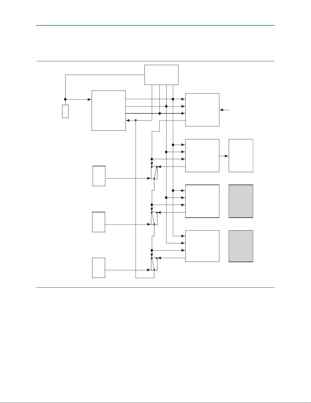
EP4SE530H35
10/100/1000
Ethernet
128 x 64
Graphic Display
RLDRAM II CIO
(x36)
Quad 7-Seg,
User LEDs Push-Button
Switches
14-pin LCD
Header
CPLD
(x32)
64 MB Flash
(x16)
4 MB SSRAM
(x32)
RJ45
Jack
Power
Measure
2.5 V
CMOS
2.5 V
CMOS
CMOS +
LVDS
2.5 V
CMOS
1.5 V/1.8 V
HSTL
2.5 V CMOS
1.5 V
SSTL
CMOS +
LVDS
100 MHz
XTAL
Port
USB
Blaster
66 MHz XTAL
4 MB QDR II+
(x18)
SMA Input
1.5 V/1.8 V
HSTL
125 MHz XTAL
SMA Output
2 GB DDR3 SDRAM DIMM (x72)
Development Board Block Diagram
Development Board Block Diagram
Figure 1–1 shows the block diagram of the Stratix IV E FPGA development board.
Figure 1–1. Stratix IV E FPGA Development Board Block Diagram
Handling the Board
c Without proper anti-static handling, the board can be damaged. Therefore, use
When handling the board, it is important to observe the following static discharge
precaution:
anti-static handling precautions when touching the board. The Stratix IV E FPGA
Stratix IV E FPGA Development Board Reference Manual May 2011 Altera Corporation
The recommended operating temperature is between 0° C and 55° C.
development board must be stored in a temperature of between –40° C and 100° C.
Page 9

Introduction
1 A complete set of schematics, a physical layout database, and GERBER files for the
f For information about powering up the board and installing the demonstration
2. Board Components
This chapter introduces the major components on the Stratix IV E FPGA development
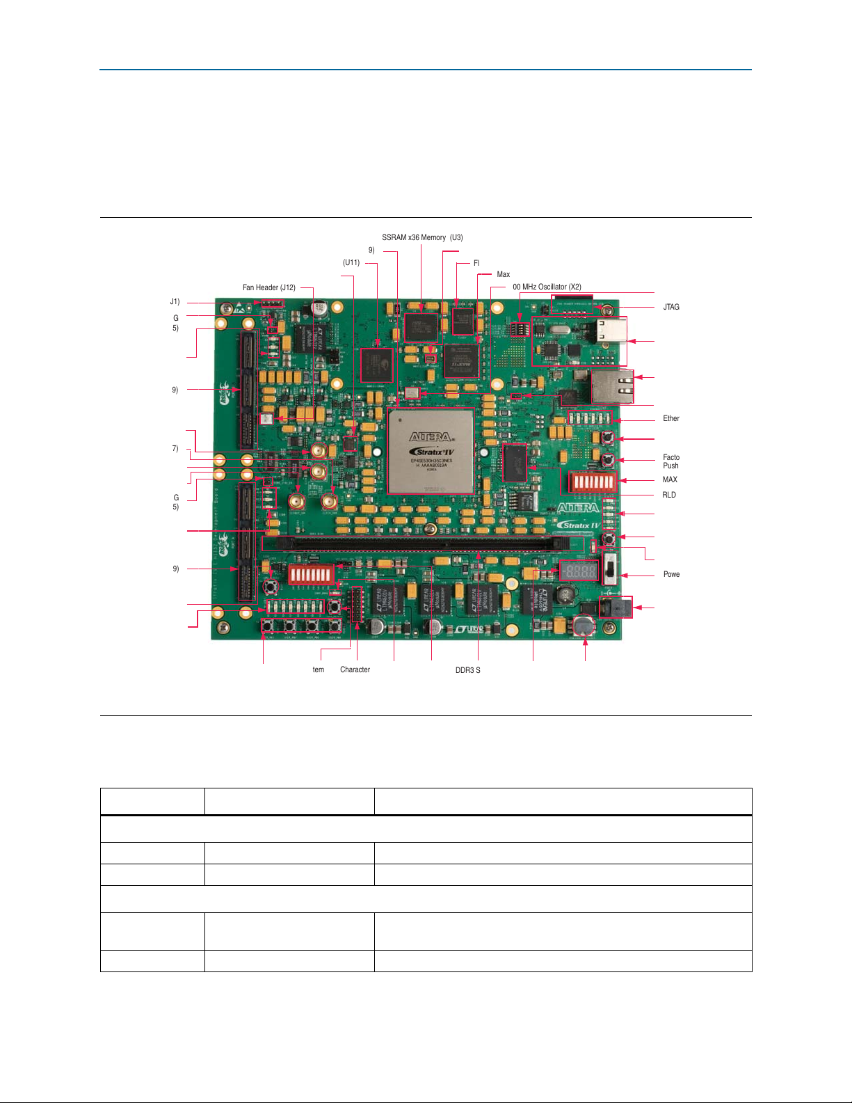
board. Figure 2–1 illustrates major component locations and Table 2–1 provides a brief
description of all component features of the board.
development board reside in the Stratix IV E FPGA development kit documents
directory.
software, refer to the Stratix IV E FPGA Development Kit User Guide.
This chapter consists of the following sections:
■ “Board Overview”
■ “Featured Device: Stratix IV E Device” on page 2–5
■ “MAX II CPLD EPM2210 System Controller” on page 2–7
■ “Configuration, Status, and Setup Elements” on page 2–12
■ “Clock Circuitry” on page 2–22
■ “General User Input/Output” on page 2–24
■ “Components and Interfaces” on page 2–31
■ “Memory” on page 2–42
■ “Power Supply” on page 2–57
■ “Statement of China-RoHS Compliance” on page 2–60
May 2011 Altera Corporation Stratix IV E FPGA Development Board Reference Manual
Page 10
2–2 Chapter 2: Board Components
HSMC Port A JTAG
Header (J15)
Character
LCD
Header
(J23)
System
Reset
Push-Button
Switch (S5)
Max II CPLD EPM2210 System Controller (U10)
DDR3 SDRAM
DIMM x72
Memory (J20)
Stratix IV E FPGA (U19)
HSMC Port B (J9)
Clock Input SMA (J17)
Speaker Header (J1)
HSMC Port A (J19)
HSMC Port B JTAG
Header (J5)
Fan Header (J12)
100 MHz Oscillator (X2)
QDRII+ x18 Memory (U11)
DC Input Jack (J22)
Power Switch (SW3)
Embedded USB-Blaster
Circuitry (J6)
JTAG Connector
(J24)
CLKIN_P SMA (J13)
HSMC Port B
Status LEDs
(D3, D4, D5)
CLKIN_N SMA (J14)
Clock Output SMA (J16)
HSMC Port A
Status LEDs
(D13, D14, D16)
CPU Reset Push-Button
Switch (S4)
User LEDs (D23-D30)
Gigabit Ethernet
Port (J8)
Ethernet LEDs
(D7-D12)
Reset Configuration
Push-Button Switch (S1)
MAX II DIP Switch (SW2)
MAX II LEDs
(D15, D17-D20)
User 1/User 2
Push-Button Switch (S3)
Power LED (D21)
Rotary Switch
(SW5)
Quad 7-Segment
Display
(U29)
User DIP
Switch
(SW4)
RLDRAM II CIO x36 (U24)
MAX II JTAG Header
(J10)
Factory Configuration
Push-Button Switch (S2)
User
Push-Button
Switches
(S6-S9)
66 MHz Oscillator (X3)
SSRAM x36 Memory (U3)
Flash x16 Memory (U2)
100 MHz Oscillator for MAX II (Y2)
Clock Enable DIP
Switch (SW1)
Configuration
Done
LED
(D22)
Board Overview
Board Overview
This section provides an overview of the Stratix IV E FPGA development board,
including an annotated board image and component descriptions. Figure 2–1
provides an overview of the development board features.
Figure 2–1. Overview of the Stratix IV E FPGA Development Board Features
Tab le 2– 1 describes the components and lists their corresponding board references.
Table 2–1. Stratix IV E FPGA Development Board Components (Part 1 of 4)
Board Reference Type Description
Featured Devices
U19 FPGA EP4SE530H35, 1152-pin FBGA.
U10 CPLD EPM2210F256, 256-pin FBGA.
Configuration, Status, and Setup Elements
J6 USB type-B connector
J24 JTAG connector (bottom side) Disables embedded blaster (for use with external USB-Blasters).
USB interface for programming the FPGA through embedded
USB-Blaster JTAG via a type-B USB cable.
Stratix IV E FPGA Development Board Reference Manual May 2011 Altera Corporation
Page 11
Chapter 2: Board Components 2–3
Board Overview
Table 2–1. Stratix IV E FPGA Development Board Components (Part 2 of 4)
Board Reference Type Description
J15 HSMC Port A JTAG header
J5 HSMC Port B JTAG header
J10 MAX II JTAG header
SW1 Clock enable DIP switch
Place a shunt on this header to include the HSMC port A in the JTAG
chain.
Place a shunt on this header to include the HSMC port B in the JTAG
chain.
Place a shunt on this header to include the MAX II CPLD EPM2210
System Controller in the JTAG chain.
Enables the oscillators when the switch is ON (positioned on the left
side of the switch).
MAX II DIP switch MAX II user DIP switches.
SW2
66 MHz oscillator select
Selects the on board oscillator when driven low and selects the
differential SMA inputs when driven high.
Selects factory or user FPGA image to load on power up. After power
SW5 Rotary switch
up, this switch selects the power rail monitored from among a total of
12 rails.
D7-D12 Ethernet LEDs
Illuminates to show the connection speed as well as transmit or
receive activity.
Illuminates when the MAX II CPLD EPM2210 System Controller is
D15, D17-D20 MAX II LEDs
actively configuring the FPGA. The LED types include
(labeled as
(labeled as
USER_1
on the board),
USER_2
on the board), and
MAX_LOAD, MAX_FACTORY, MAX_PB
MAX_ERROR
MAX_EMB
.
D21 Power LED Illuminates when power is present.
D22 Configuration done LED Illuminates when the FPGA is configured.
D13, D14 HSMC port A status LEDs You can configure these LEDs to indicate transmit or receive activity.
D16 HSMC port A present LED Illuminates when a daughtercard is plugged into the HSMC port A.
D3, D4 HSMC port B status LEDs You can configure these LEDs to indicate transmit or receive activity.
D5 HSMC port B present LED Illuminates when a daughtercard is plugged into the HSMC port B.
Clock Circuitry
X2 100 MHz oscillator 100.0 MHz crystal oscillator to the FPGA.
66.6 MHz crystal oscillator with a single-ended input to the LVDS clock
buffer (U22). This oscillator is also MUXed with the differential SMA
X3 66 MHz oscillator
clock inputs (J13 and J14) based on the
CLK66_SEL
signal needs to be set to '0' on SW2 to enable the
CLK66_SEL
input. The
oscillator clock source. Two LVDS clocks are output from the clock
buffer to the FPGA.
X4 125 MHz oscillator
X5 50 MHz oscillator
Y2
100 MHz oscillator
(for MAX II CPLD)
125.000 MHz crystal oscillator to the LVDS clock buffer. Two LVDS
clocks are output from the clock buffer to the FPGA.
50 MHz single-ended oscillator to the FPGA and MAX II CPLD
EPM2210 System Controller.
100 MHz single-ended dedicated clock oscillator to the MAX II CPLD
EPM2210 System Controller.
J17 Clock input SMAs Drives LVPECL-compatible clock inputs into the FPGA.
J16 Clock output SMA Drives out 2.5-V CMOS clock output from the FPGA.
May 2011 Altera Corporation Stratix IV E FPGA Development Board Reference Manual
Page 12
2–4 Chapter 2: Board Components
Board Overview
Table 2–1. Stratix IV E FPGA Development Board Components (Part 3 of 4)
Board Reference Type Description
J13 CLKIN_P SMA (positive) Drives LVPECL-compatible differential clock inputs into the LVDS clock
J14 CLKIN_N SMA (negative)
buffer (U22).The
CLK66_SEL
enable the SMA clock source. Two LVDS clocks are output from the
signal needs to be set to '1' on SW2 to
clock buffer to the FPGA.
General User Input/Output
SW4 User DIP switch
S1
S2
S3
Reset configuration
push-button switch
Factory configuration
push-button switch
User 1 /User 2 push-button
switch
Connects directly to the FPGA. When the switch is ON, a logic 0 is
selected.
Press to reconfigure the FPGA from flash memory.
Press to reconfigure the FPGA to the factory default design.
User-defined push-button switch. Driven to the MAX II CPLD EPM2210
System Controller.
S4 CPU reset push-button switch Press to reset the FPGA logic.
S5
System reset push-button
switch
Press to reset the MAX II CPLD EPM2210 System Controller and FPGA
logic.
S6-S9 User push-button switches Four user push-button switches. Driven low when pressed.
D23-D30 User LEDs Illuminates when driven low.
Display Ports
J23 Character LCD header
Header which interfaces to the provided 16 character × 2 line LCD
module along with two standoffs.
Quad digit seven-segment LED display. The display is controlled by the
U29 Seven-segment LED
Stratix IV E FPGA device. Each segment of the display can be
illuminated by driving a logic 0 to the connected device's I/O pin.
Connector to plug in the flex cable from the 128 × 64 graphics display.
Lift the connector latch to plug in the flex cable, and then close the
latch.
J27
Graphics LCD connector
(bottom side)
Components and Interfaces
J19 HSMC port A Provides 17 LVDS channels per the HSMC specification.
J9 HSMC port B Provides 17 LVDS channels per the HSMC specification.
RJ-45 connector providing a 10/100/1000 Ethernet connection via a
J8 Gigabit Ethernet
Marvell 88E1111 PHY and interfaces to the FPGA-based Altera Triple
Speed Ethernet MegaCore function in SGMII mode.
J12 Fan header Header to plug in the fan.
J1 Speaker header Optional speaker header for user design.
Memory Devices
DDR3 SDRAM DIMM (256 M x 72) 240-pin connector, populated with
a dual rank 2-GB memory module, and interfaces with a 72-bit data
width on the Vertical I/O (VIO) banks.
J20
DDR3 SDRAM DIMM x72
memory
U24 RLDRAM II CIO x36 memory 533-MHz RLDRAM II CIO device in a 16 M x 36 configuration.
U11 QDR II+ x18 memory
QDR II+ SRAM device in a 4 M x 18 configuration for high-speed,
low-latency memory access.
Stratix IV E FPGA Development Board Reference Manual May 2011 Altera Corporation
Page 13
Chapter 2: Board Components 2–5
Featured Device: Stratix IV E Device
Table 2–1. Stratix IV E FPGA Development Board Components (Part 4 of 4)
Board Reference Type Description
A single 250-MHz 18-Mb (2 M x 36) SSRAM device with a 165-BGA
U3 SSRAM x36 memory
U2 Flash x16 memory
Power Supply
J22 DC input jack Accepts a 14-V – 20-V DC power supply.
SW3 Power switch
package footprint. This footprint allows for both Flow-Through and
Pipelined devices (single or dual cycle deselect).
Embedded memory device which provides a 16-bit 64-MB non-volatile
memory port.
Switch to power on or off the board when power is supplied from the
DC input jack.
Featured Device: Stratix IV E Device
The Stratix IV E FPGA development board features the Stratix IV E EP4SE530H35
device (U19) in a 1152-pin FBGA package.
f For more information about the Stratix IV device family, refer to the Stratix IV Device
Handbook.
Tab le 2– 2 describes the features of the Stratix IV E EP4SE530H35 device.
Table 2–2. Stratix IV E EP4SE530H35 Device Features
ALMs
212,480 531,200 1,280 64 27,376 1,024 736 8 1152-pin FBGA
Equivalent
LEs
M9K RAM
Blocks
M144K RAM
Blocks
Total RAM
bits
18-bit × 18-bit
Multipliers
Maximum
User I/O Pins
PLLs Package Type
Tab le 2– 3 lists the Stratix IV E EP4SE530H35 component reference and manufacturing
information.
Table 2–3. Stratix IV E EP4SE530H35 Device Component Reference and Manufacturing Information
Board Reference Description Manufacturer
U19 FPGA, Stratix IV E F1152, leadfree Altera
Corporation EP4SE530H35C2N www.altera.com
Manufacturing
Part Number
Manufacturer
Website
May 2011 Altera Corporation Stratix IV E FPGA Development Board Reference Manual
Page 14
2–6 Chapter 2: Board Components
EP4SE290
EP4SE360
EP4SE530
EP4SE680
Bank 8B 24
Bank 7A 40
Bank 7B 24
Bank 7C 32
40 Bank 1C
40 Bank 2C
24 Bank 3B
40 Bank 4A
24 Bank 4B
32 Bank 4C
Bank 6C 40
Bank 5C 40
48 Bank 2A
Bank 8C 32
Bank 8A 40
32 Bank 3C
40 Bank 3A
Bank 5A 48
Bank 6A 48
Bank
Name
Number
of I/Os
Bank
Name
Number
of I/Os
48 Bank 1A
Featured Device: Stratix IV E Device
I/O Resources
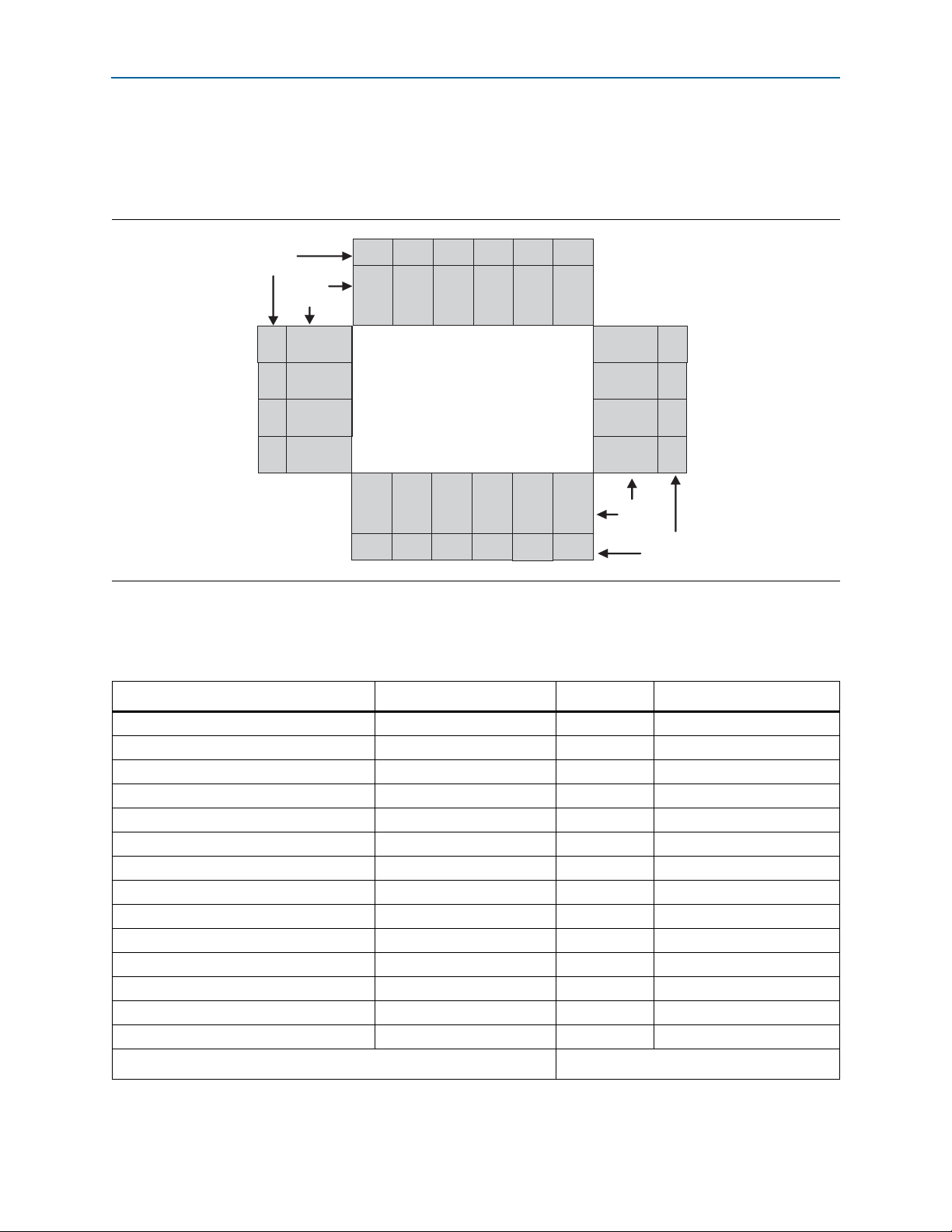
Figure 2–2 illustrates the bank organization and I/O count for the EP4SE530 device in
the 1152-pin FBGA package.
Figure 2–2. EP4SE530 Device I/O Bank Diagram
Tab le 2– 4 lists the Stratix IV E device pin count and usage by function on the
development board.
Table 2–4. Stratix IV E Device Pin Count and Usage
Function I/O Standard I/O Count Special Pins
OSC/SMAs 1.5-V/2.5-V CMOS 13 12 Clock Inputs, 1 Output
DDR3 DIMM 1.5-V SSTL 153 18 DQS pins
QDR II+ 1.5-V HSTL 69 2 CQ pins
RLDRAM II CIO 1.5-V HSTL 77 —
HSMC Port A 2.5-V CMOS + LVDS 86 3 Clock Inputs
HSMC Port B 2.5-V CMOS + LVDS 86 3 Clock Inputs
Flash, SSRAM, MAX 2.5-V CMOS 91 —
Gigabit Ethernet 2.5-V CMOS 36 —
User I/O (LEDs, DIP Switch, Push-Buttons) 1.5-V/2.5-V CMOS 21 —
14-pin LCD Header 2.5-V CMOS 11 —
Graphic Display 2.5-V CMOS 15 —
Seven-Segment Display 2.5-V CMOS 13 —
EEPROM 2.5-V CMOS 4 —
MAX II Control, Speaker 2.5-V CMOS 6 —
Device I/O Total:
681
Stratix IV E FPGA Development Board Reference Manual May 2011 Altera Corporation
Page 15
Chapter 2: Board Components 2–7
MAX1619
Controller
Information
Register
EMB
Blaster
MAX II Device
SLD-HUB
PFL
FSM BUS
Power
Measure
Results
Virtual-JTAG
PC
Temperature
Measure
Results
FPGA
LTC2418
Controller
FLASH
Decoder
Encoder
GPIO
JTAG Control
SRAM
Control
Register
Fast Configuration
Downloader
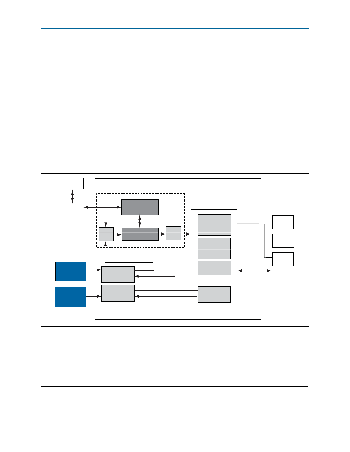
MAX II CPLD EPM2210 System Controller
MAX II CPLD EPM2210 System Controller
The board utilizes the EPM2210 System Controller, an Altera MAX II CPLD, for the
following purposes:
■ FPGA configuration from flash memory
■ Power consumption monitoring
■ Temp er a ture m on it or in g
■ Fan control
■ Virtual JTAG interface for PC-based power and temperature GUI
■ Control registers for clocks
■ Control registers for remote system update
Figure 2–3 illustrates the MAX II CPLD EPM2210 System Controller's functionality
and external circuit connections as a block diagram.
Figure 2–3. MAX II CPLD EPM2210 System Controller Block Diagram
Table 2–5. MAX II CPLD EPM2210 System Controller Device (U10) Pin-Out (Part 1 of 5)
Schematic Signal Name
2.5V_FPGA_PG
2.5V_HSMC_PG
May 2011 Altera Corporation Stratix IV E FPGA Development Board Reference Manual
Tab le 2– 5 lists the I/O signals present on the MAX
Controller. The signal names and functions are relative to the MAX
I/O
Standard
EPM2210
Pin Number
Stratix IV E
Device
Pin Number
Other
Connections
2.5-V E9 — U41.7 FPGA 2.5-V power good monitor
2.5-V A7 — U26.7 HSMC 2.5-V power good monitor
II CPLD EPM2210 System
II device (U10).
Description
Page 16
2–8 Chapter 2: Board Components
MAX II CPLD EPM2210 System Controller
Table 2–5. MAX II CPLD EPM2210 System Controller Device (U10) Pin-Out (Part 2 of 5)
Schematic Signal Name
3.3V_PG
CLK100_EN
CLK125_EN
CLK50_EN
CLK66_EN
CLK66_SEL
CLKIN_50
CLKIN_MAX_100
FACTORY_CONFIGn
FLASH_ADVn
FLASH_CEn
FLASH_CLK
FLASH_OEn
FLASH_RDYBSYn
FLASH_RESETn
FLASH_WEn
FPGA_CONF_DONE
FPGA_CONFIGn
FPGA_DATA0
FPGA_DATA1
FPGA_DATA2
FPGA_DATA3
FPGA_DATA4
FPGA_DATA5
FPGA_DATA6
FPGA_DATA7
FPGA_DCLK
FPGA_STATUSn
FSM_A0
FSM_A1
FSM_A2
FSM_A3
FSM_A4
FSM_A5
FSM_A6
I/O
Standard
EPM2210
Pin Number
Stratix IV E
Device
Pin Number
Other
Connections
Description
2.5-V E8 — U9.G12 3.3-V power good monitor
2.5-V J1 — SW1.3, X2.1 100 MHz oscillator enable
2.5-V J2 — SW1.4, X4.1 125 MHz oscillator enable
2.5-V H3 — SW1.1, X5.1 50 MHz oscillator enable
2.5-V H4 — SW1.2, X3.1 66 MHz oscillator enable
2.5-V L14 — SW2.8, U22.3 DIP-clock select SMA or oscillator
2.5-V J12 J12 X5.3 50 MHz clock input
2.5-V H12 — Y2.3
2.5-V A10 — S2.2
2.5-V L13 D20 U2.F6
100 MHz oscillator to the MAX II
CPLD EPM2210 System Controller
Load factory or user design at
power-up
FSM bus flash memory address
valid
2.5-V K14 K25 U2.B4 FSM bus flash memory chip enable
2.5-V L15 K24 U2.E6 FSM bus flash memory clock
2.5-V M16 K23 U2.F8
FSM bus flash memory output
enable
2.5-V L11 C20 U2.F7 FSM bus flash memory ready
2.5-V M15 G21 U2.D4 FSM bus flash memory reset
2.5-V L12 L22 U2.G8 FSM bus flash memory write enable
2.5-V E3 AH29 — FPGA configuration done
2.5-V E4 AE25 — FPGA configuration active
2.5-V D3 T28 — FPGA configuration data
2.5-V L1 T27 — FPGA configuration data
2.5-V K5 R34 — FPGA configuration data
2.5-V L2 R33 — FPGA configuration data
2.5-V K4 T25 — FPGA configuration data
2.5-V M1 T24 — FPGA configuration data
2.5-V K3 T32 — FPGA configuration data
2.5-V M2 R31 — FPGA configuration data
2.5-V C2 AL3 — FPGA configuration clock
2.5-V C3 AH28 — FPGA configuration ready
2.5-V N9 F22 — FSM bus address
2.5-V T8 H23 U2.A1 FSM bus address
2.5-V T9 G23 U3.R6, U2.B1 FSM bus address
2.5-V R9 F23 U3.P6, U2.C1 FSM bus address
2.5-V P9 D27 U3.A2, U2.D1 FSM bus address
2.5-V T10 D28 U3.A10, U2.D2 FSM bus address
2.5-V P13 F25 U3.B2, U2.A2 FSM bus address
Stratix IV E FPGA Development Board Reference Manual May 2011 Altera Corporation
Page 17
Chapter 2: Board Components 2–9
MAX II CPLD EPM2210 System Controller
Table 2–5. MAX II CPLD EPM2210 System Controller Device (U10) Pin-Out (Part 3 of 5)
Schematic Signal Name
FSM_A7
FSM_A8
FSM_A9
FSM_A10
FSM_A11
FSM_A12
FSM_A13
FSM_A14
FSM_A15
FSM_A16
FSM_A17
FSM_A18
FSM_A19
FSM_A20
FSM_A21
FSM_A22
FSM_A23
FSM_A24
FSM_A25
FSM_A26
FSM_D0
FSM_D1
FSM_D2
FSM_D3
FSM_D4
FSM_D5
FSM_D6
FSM_D7
FSM_D8
FSM_D9
FSM_D10
FSM_D11
FSM_D12
FSM_D13
FSM_D14
FSM_D15
FSM_D16
FSM_D17
I/O
Standard
EPM2210
Pin Number
Stratix IV E
Device
Pin Number
Other
Connections
2.5-V R10 F26 U3.B10, U2.C2 FSM bus address
2.5-V M10 G24 U3.N6, U2.A3 FSM bus address
2.5-V T11 F24 U3.P3, U2.B3 FSM bus address
2.5-V N10 E26 U3.P4, U2.C3 FSM bus address
2.5-V R11 D26 U3.P8, U2.D3 FSM bus address
2.5-V P10 A30 U3.P9, U2.C4 FSM bus address
2.5-V T12 A33 U3.P10, U2.A5 FSM bus address
2.5-V M11 B31 U3.P11, U2.B5 FSM bus address
2.5-V R12 A31 U3.R3, U2.C5 FSM bus address
2.5-V N11 B32 U3.R4, U2.D7 FSM bus address
2.5-V T13 A32 U3.R8, U2.D8 FSM bus address
2.5-V P11 M23 U3.R9, U2.A7 FSM bus address
2.5-V R13 L23 U3.R10, U2.B7 FSM bus address
2.5-V M12 B29 U3.R11, U2.C7 FSM bus address
2.5-V R14 C29 U3.B1, U2.C8 FSM bus address
2.5-V N12 C31 U3.A1, U2.A8 FSM bus address
2.5-V T15 D31 U3.B11, U2.G1 FSM bus address
2.5-V P12 F27 U3.C10, U2.H8 FSM bus address
2.5-V E13 D18 U3.P2, U2.B6 FSM bus address
2.5-V J16 W10 U2.B8 FSM bus address
2.5-V P4 G27 U3.J10, U2.F2 FSM bus data
2.5-V R1 F28 U3.J11, U2.E2 FSM bus data
2.5-V P5 E28 U3.K10, U2.G3 FSM bus data
2.5-V T2 D30 U3.K11, U2.E4 FSM bus data
2.5-V N5 C30 U3.L10, U2.E5 FSM bus data
2.5-V R3 F29 U3.L11, U2.G5 FSM bus data
2.5-V P6 E29 U3.M10, U2.G6 FSM bus data
2.5-V R4 J24 U3.M11, U2.H7 FSM bus data
2.5-V N6 J25 U3.D10, U2.E1 FSM bus data
2.5-V T4 A24 U3.D11, U2.E3 FSM bus data
2.5-V M6 A26 U3.E10, U2.F3 FSM bus data
2.5-V R5 B25 U3.E11, U2.F4 FSM bus data
2.5-V P7 A25 U3.F10, U2.F5 FSM bus data
2.5-V T5 J20 U3.F11, U2.H5 FSM bus data
2.5-V N7 K20 U3.G10, U2.G7 FSM bus data
2.5-V R6 K21 U3.G11, U2.E7 FSM bus data
2.5-V M7 K22 U3.D1 FSM bus data
2.5-V T6 C26 U3.D2 FSM bus data
Description
May 2011 Altera Corporation Stratix IV E FPGA Development Board Reference Manual
Page 18

2–10 Chapter 2: Board Components
MAX II CPLD EPM2210 System Controller
Table 2–5. MAX II CPLD EPM2210 System Controller Device (U10) Pin-Out (Part 4 of 5)
Stratix IV E
Device
Pin Number
Other
Connections
J24.1, U8.L9,
J9.35, J19.35
J24.5, U8.J11,
J9.36, J19.36
Description
JTAG clock signal
JTAG mode select signal
Schematic Signal Name
FSM_D18
FSM_D19
FSM_D20
FSM_D21
FSM_D22
FSM_D23
FSM_D24
FSM_D25
FSM_D26
FSM_D27
FSM_D28
FSM_D29
FSM_D30
FSM_D31
HSMA_PSNTn
HSMB_PSNTn
JTAG_EPM2210_TDO
JTAG_FPGA_TDO
JTAG_TCK
I/O
Standard
2.5-V P14 B26 U3.E1 FSM bus data
2.5-V R7 J22 U3.E2 FSM bus data
2.5-V P8 J21 U3.F1 FSM bus data
2.5-V T7 C24 U3.F2 FSM bus data
2.5-V N8 E25 U3.G1 FSM bus data
2.5-V R8 D25 U3.G2 FSM bus data
2.5-V F12 D24 U3.J1 FSM bus data
2.5-V D16 A27 U3.J2 FSM bus data
2.5-V F13 A29 U3.K1 FSM bus data
2.5-V D15 C27 U3.K2 FSM bus data
2.5-V F14 C28 U3.L1 FSM bus data
2.5-V D14 E23 U3.L2 FSM bus data
2.5-V E12 D23 U3.M1 FSM bus data
2.5-V C15 B28 U3.M2 FSM bus data
2.5-V F16 — J19.160, R189 HSMC port A present
2.5-V G13 — J9.160, R189 HSMC port B present
2.5-V M5 — U35.5 JTAG data output for MAX II
2.5-V L6 G29 U35.2 JTAG data output for FPGA
2.5-V P3 F30
EPM2210
Pin Number
JTAG_TMS 2.5-V N4 H28
MAX_CLK 2.5-V H5 N3 — FSM bus MAX II clock
MAX_CSn 2.5-V L16 N29 — FSM bus MAX II chip select
MAX_DIP0
MAX_DIP1
MAX_DIP2
MAX_DIP3
MAX_DIP4
MAX_DIP5
MAX_DIP6
MAX_EMB 2.5-V E15 — D15
MAX_ERROR
MAX_FACTORY
MAX_LOAD
2.5-V E14 — SW2.1 DIP - reserved
2.5-V D13 — SW2.2 DIP - reserved
2.5-V K16 — SW2.3 DIP - reserved
2.5-V N2 — SW2.4 DIP - reserved
2.5-V N14 — SW2.5 DIP - reserved
2.5-V M13 — SW2.6 DIP - reserved
2.5-V N15 — SW2.7 DIP - reserved
User-defined push-button switch
(labeled as
USER_1
on the board)
2.5-V H15 — D20 FPGA configuration error LED
2.5-V G16 — D18 FPGA factory configuration LED
2.5-V H14 — D17 FPGA configuration active LED
MAX_OEn 2.5-V K13 K27 — FSM bus MAX II output enable
MAX_PB 2.5-V D4 — S3
User-defined push-button switch
(labeled as
USER_2
on the board)
Stratix IV E FPGA Development Board Reference Manual May 2011 Altera Corporation
Page 19
Chapter 2: Board Components 2–11
MAX II CPLD EPM2210 System Controller
Table 2–5. MAX II CPLD EPM2210 System Controller Device (U10) Pin-Out (Part 5 of 5)
Stratix IV E
Device
Pin Number
Other
Connections
Description
Power regulator 0 degrees phase
control
Power regulator 180 degrees phase
control
Schematic Signal Name
I/O
Standard
EPM2210
Pin Number
MAX_PHASE_CLK0 2.5-V J4 — U30.A8
MAX_PHASE_CLK180 2.5-V K1 — U33.B9
MAX_TO_STRATIX4 2.5-V H1 K1 — Optional pin for user function
MAX_USER
2.5-V G12 — D19
User-defined LED (labeled as
USER_1/USER_2
on the board)
MAX_WEn 2.5-V K15 K28 — FSM bus MAX II write enable
OVERTEMP 2.5-V M4 — Q1 Fan speed control
OVERTEMPn 2.5-V E7 — U18.9
Temperature monitor
over-temperature indicator
PGM0 2.5-V N13 — SW5.1 Rotary switch input
PGM1 2.5-V P15 — SW5.2 Rotary switch input
PGM2 2.5-V M14 — SW5.4 Rotary switch input
PGM3 2.5-V N16 — SW5.8 Rotary switch input
PHASE0 2.5-V C13 — U49.4 Power clock 0 degrees
PHASE90 2.5-V B16 — U49.5, U36.A8 Power clock 90 degrees
PHASE180 2.5-V C12 — U49.6, U29.A8 Power clock 180 degrees
PHASE270 2.5-V A15 — U49.7, U6.A8 Power clock 270 degrees
RESET_CONFIGn 2.5-V R16 — S1
Force FPGA configuration
push-button switch
SENSE_ADC_F0 2.5-V E2 — U44.2 Power monitor frequency
SENSE_CS0n 2.5-V F5 — U43.3 Power monitor 0 chip select
SENSE_CS1n 2.5-V F2 — U43.2 Power monitor 1 chip select
SENSE_SCK 2.5-V E1 — U44.5 Power monitor SPI clock
SENSE_SDI 2.5-V F4 — U44.4 Power monitor SPI data in
SENSE_SDO 2.5-V F3 — U44.3 Power monitor SPI data out
SSRAM_GWn 2.5-V E11 — U3.B7 FSM bus SSRAM global write enable
SSRAM_MODE 2.5-V D11 — U3.R1
FSM bus SSRAM burst sequence
selection
SSRAM_ZZ 2.5-V A13 — U3.H11 FSM bus SSRAM power sleep mode
SYS_RESETn 2.5-V M9 U31 S5 User-defined reset
TSENSE_ALERTN 2.5-V J5 — U18.11 Temperature monitor alert
TSENSE_SMB_CLK 2.5-V L3 — U18.14, U21.6 Temperature monitor SMB clock
TSENSE_SMB_DATA 2.5-V N1 — U18.12, U21.7 Temperature monitor SMB data
VDDQ_QDRII_PG 2.5-V A9 — U16.7 I/O supply
May 2011 Altera Corporation Stratix IV E FPGA Development Board Reference Manual
Page 20

2–12 Chapter 2: Board Components
Configuration, Status, and Setup Elements
Tab le 2– 6 lists the MAX II CPLD EPM2210 System Controller component reference
and manufacturing information.
Table 2–6. MAX II CPLD EPM2210 System Controller Component Reference and Manufacturing Information
Board Reference Description Manufacturer
U10
IC - MAX II CPLD EPM2210
256FBGA -3 LF 2.5V VCCINT
Altera
Corporation EPM2210F256C3N www.altera.com
Configuration, Status, and Setup Elements
This section describes the board's configuration, status, and setup elements.
Configuration
This section describes the FPGA, flash memory, and MAX II CPLD EPM2210 System
Controller device programming methods supported by the Stratix IV E FPGA
development board. The Stratix IV E FPGA development board supports the
following three configuration methods:
■ Embedded USB-Blaster is the default method for configuring the FPGA at any
time using the Quartus II Programmer in JTAG mode with the supplied USB cable.
■ Flash memory programming using the Board Update Portal factory design.
■ FPGA Programming from Flash memory for configuring the FPGA using stored
images from the flash memory on either power-up or pressing the reset
configuration push-button switch (S1).
Manufacturing
Part Number
Manufacturer
Website
FPGA Programming over Embedded USB-Blaster
The USB-Blaster is implemented using a USB Type-B connector (J6), a FTDI USB 2.0
PHY device (U7), and an Altera MAX II CPLD (U10). This allows the configuration of
the FPGA using a USB cable directly connected between the USB port on the board
(J6) and a USB port of a PC running the Quartus II software. The JTAG chain is
normally mastered by the embedded USB-Blaster found in the MAX
EPM2210 System Controller.
II CPLD
Stratix IV E FPGA Development Board Reference Manual May 2011 Altera Corporation
Page 21
Chapter 2: Board Components 2–13
Embedded
Blaster
GPIO
TCK
EP4S530
FPGA
Analog
Switch
MAX II CPLD
EPM2210
System
Controller
HSMC
Port A
HSMC
Port B
GPIO
TMS
GPIO
TDO
GPIO
TDI
JTAG Master
GPIO
DISABLE
JTAG Master/Slave
JTAG Master/Slave
Installed
HSMC
Card
Installed
HSMC
Card
TCK
TMS
TDI
TDO
TCK
TMS
TDI
TDO
TCK
TMS
TDI
TDO
TCK
TMS
TDI
TDO
JTAG Slave
JTAG Slave
Analog
Switch
Analog
Switch
ENABLE
ALWAYS
ENABLED
(in chain)
Jumper
10-pin
JTAG Connector
Flash
Memory
(on install)
J10
Jumper
Jumper
Jumper
J15
J5
ENABLE
ENABLE
J4
Configuration, Status, and Setup Elements
The embedded USB-Blaster is automatically disabled when an external USB-Blaster is
connected to the JTAG chain. Figure 2–4 illustrates the JTAG chain.
Figure 2–4. JTAG Chain
Each jumper shown in Figure 2–4 is located near its corresponding interface. To
connect a device or interface in the chain, the corresponding shunt must be installed
1 A board must be plugged into the HSMC port in order for the chain to be contiguous.
May 2011 Altera Corporation Stratix IV E FPGA Development Board Reference Manual
to the jumper. The FPGA, by default, is always in the chain.
If there is a shunt on the jumper without a board plugged in to the corresponding
HSMC port, the chain is broken and configuration cannot be performed.
The MAX
II CPLD EPM2210 System Controller must be in the chain to use some of the
GUI interfaces. For this setting, place a jumper shunt on the MAX II JTAG header
(J10).
Page 22
2–14 Chapter 2: Board Components
Configuration, Status, and Setup Elements
Flash Memory Programming
Flash memory programming is possible through a variety of methods using the
Stratix IV E device.
The default method is to use the factory design called the Board Update Portal. This
design is an embedded webserver, which serves the Board Update Portal web page.
The web page allows you to select new FPGA designs including hardware, software,
or both in an industry-standard S-Record File (.flash) and write the design to the user
hardware page (page 1) of the flash memory over the network.
The secondary method is to use the pre-built parallel flash loader (PFL) design
included in the development kit. The development board implements the Altera PFL
megafunction for flash memory programming. The PFL megafunction is a block of
logic that is programmed into an Altera programmable logic device (FPGA or CPLD).
The PFL functions as a utility for writing to a compatible flash memory device. This
pre-built design contains the PFL megafunction that allows you to write either page 0,
page 1, or other areas of flash memory over the USB interface using the Quartus II
software. This method is used to restore the development board to its factory default
settings.
Other methods to program the flash memory can be used as well, including the
®
Nios
II processor.
f For more information on the Nios II processor, refer to the Nios II Processor page of
the Altera website.
FPGA Programming from Flash Memory
On either power-up or by pressing the reset configuration push-button switch (S1),
the MAX
flash memory. The PFL megafunction reads 16-bit data from the flash memory and
converts it to fast passive parallel (FPP) format. This 8-bit data is then written to the
FPGA's dedicated configuration pins during configuration. The bit stream loaded into
the FPGA is selected by the PGM rotary switch (SW5) connected to the MAX
EPM2210 System Controller.
Figure 2–5 illustrates the connection for FPGA programming from flash memory.
Figure 2–5. FPGA Programming from Flash Memory
Flash Memory
Rotary Switch
II CPLD EPM2210 System Controller's PFL configures the FPGA from the
Flash Data
PGM
EPM2210F256
CPLD
Fast Passive Parallel
(FPP)
EP4SE530H35
II CPLD
Stratix IV E FPGA Development Board Reference Manual May 2011 Altera Corporation
Page 23

Chapter 2: Board Components 2–15
Configuration, Status, and Setup Elements
Tab le 2– 7 shows the flash memory map storage.
Table 2–7. Flash Memory Map
Block Description Size Address Range
Unused 32 KB
Unused 32 KB
Unused 32 KB
Unused 32 KB
User software 11,669 KB
User hardware 21,627 KB
Reserved 128 KB
zipfs (html, web content) 5,898 KB
Factory software 5,898 KB
Factory hardware 21,627 KB
PFL option bits 32 KB
Reserved 32 KB
Ethernet option bits 32 KB
0x03FF8000 - 0x03FFFFFF
0x03FF0000 - 0x03FF7FFF
0x03FE8000 - 0x03FEFFFF
0x03FE0000 - 0x03FE7FFF
0x034C0000 - 0x03FDFFFF
0x02020000 - 0x034BFFFF
0x02000000 - 0x0201FFFF
0x01A60000 - 0x01FFFFFF
0x014C0000 - 0x01A5FFFF
0x00020000 - 0x014BFFFF
0x00018000 - 0x0001FFFF
0x00010000 - 0x00017FFF
0x00008000 - 0x0000FFFF
User design reset vector 32 KB 0x00000000 - 0x00007FFF
There are two pages reserved for the FPGA configuration data. The factory hardware
page is considered page 0 and is loaded upon power-up if the rotary switch is set to
'0'. Otherwise, the user hardware page 1 is loaded.
f For more information on the following topics, refer to the respective documents:
■ Board Update Portal, refer to the Stratix IV E FPGA Development Kit User Guide.
■ PFL design, refer to the Stratix IV E FPGA Development Kit User Guide.
■ PFL megafunction, refer to AN 386: Using the Parallel Flash Loader with the Quartus
II Software.
Status Elements
The development board includes general user, board specific, and status LEDs. This
section describes the status elements.
May 2011 Altera Corporation Stratix IV E FPGA Development Board Reference Manual
Page 24

2–16 Chapter 2: Board Components
Configuration, Status, and Setup Elements
Tab le 2– 8 lists the LED board references, names, and functional descriptions.
Table 2–8. Board-Specific LEDs (Part 1 of 2)
Stratix IV
Board
Reference
Schematic Signal Name Description
I/O
Standard
E Device
Pin
Other
Connections
Number
Green LED. Illuminates to indicate Ethernet
D11
ENET_LED_TX
PHY transmit activity. Driven by the Marvell
——
88E1111 PHY.
Green LED. Illuminates to indicate Ethernet
D12
ENET_LED_RX
PHY receive activity. Driven by the Marvell
——
88E1111 PHY.
Green LED. Illuminates to indicate Ethernet
D7
ENET_LED_LINK10
linked at 10 Mbps connection speed.
——
Driven by the Marvell 88E1111 PHY.
Green LED. Illuminates to indicate Ethernet
D8
ENET_LED_LINK100
linked at 100 Mbps connection speed.
——
Driven by the Marvell 88E1111 PHY.
Green LED. Illuminates to indicate Ethernet
D9
ENET_LED_LINK1000
linked at 1000 Mbps connection speed.
N32 —
Driven by the Marvell 88E1111 PHY.
Green LED. Illuminates to indicate Ethernet
D10
D15
ENET_LED_DUPLEX
MAX_EMB
(labeled
USER_1
on the board)
PHY is operating in Duplex mode. Driven
by the Marvell 88E1111 PHY.
Green LED. Illuminates to indicate which
configuration page is loaded.
——
2.5-V
— U10.E15
Green LED. Illuminates when the MAX II
CPLD EPM2210 System Controller is
D17
MAX_LOAD
actively configuring the FPGA. Driven by
— U10.H14
the MAX II CPLD EPM2210 System
Controller.
D18
D19
MAX_FACTORY
MAX_USER
USER_2
(labeled
on the board)
Green LED. Illuminates when FPGA is
configured with the default factory design.
Green LED. Illuminates to indicate which
configuration page is loaded.
— U10.G16
— U10.G12
Red LED. Illuminates when the MAX II
D20
MAX_ERROR
CPLD EPM2210 System Controller fails to
configure the FPGA. Driven by the MAX II
— U10.H15
CPLD EPM2210 System Controller.
Green LED. Illuminates when the FPGA is
D22
FPGA_CONF_DONE
successfully configured. Driven by the
AH29 U10.E3
MAX II CPLD EPM2210 System Controller.
D21
12V
Blue LED. Illuminates when 12-V power rail
is active.
—— —
Stratix IV E FPGA Development Board Reference Manual May 2011 Altera Corporation
Page 25

Chapter 2: Board Components 2–17
Configuration, Status, and Setup Elements
Table 2–8. Board-Specific LEDs (Part 2 of 2)
Stratix IV
Board
Reference
Schematic Signal Name Description
I/O
Standard
E Device
Pin
Other
Connections
Number
Green LEDs. Illuminates when HSMC port
D16 HSMA_PSNTn
D5 HSMB_PSNTn
A has a board or cable plugged-in such that
pin 160 becomes grounded. Driven by the
add-in card.
Green LEDs. Illuminates when HSMC port
B has a board or cable plugged-in such that
pin 160 becomes grounded. Driven by the
——
2.5-V
——
add-in card.
Tab le 2– 9 lists the board-specific LEDs component references and manufacturing
information.
Table 2–9. Board-Specific LEDs Component References and Manufacturing Information
Board Reference Description Manufacturer
Manufacturer
Part Number
Manufacturer Website
D5, D7-D19, D22-D30 Green LEDs Lumex Inc. SML-LX1206GC-TR www.lumex.com
D20 Red LED Lumex Inc. SML-LX1206IC-TR www.lumex.com
D21 Blue LED Lumex Inc. SML-LX1206USBC-TR www.lumex.com
Setup Elements
The development board includes several different kinds of setup elements. This
section describes the following setup elements:
■ MAX II DIP switch
■ User DIP switch
■ Clock enable DIP switch
■ JTAG chain jumpers
■ On-Board memory headers
■ Reset configuration push-button switch
■ Rotary switch
May 2011 Altera Corporation Stratix IV E FPGA Development Board Reference Manual
Page 26

2–18 Chapter 2: Board Components
Configuration, Status, and Setup Elements
MAX II DIP Switch
The MAX II DIP switch (SW2) provides user-specific control settings for the MAX II
CPLD EPM2210 System Controller logic design. There is a 66-MHz clock select switch
which is used to select between the on-board oscillator or the user-defined external
clock source supplied on the SMA inputs. Tab le 2– 10 shows the switch controls and
descriptions.
Table 2–10. MAX II DIP Switch Controls
Board
Reference
SW2.1
SW2.2
SW2.3
SW2.4
SW2.5
SW2.6
SW2.7
SW2.8
Schematic
Signal Name
DIP0
DIP1
DIP2
DIP3
DIP4
DIP5
DIP6
CLK66_SEL
Description
MAX II user-defined DIP switch. When
the switch is in the OPEN or OFF position,
a logic 1 is selected. When the switch is
in the CLOSED or ON position, a logic 0
is selected.
Selects either the on-board oscillator or
the SMA inputs.
ON : SMA input clock select
OFF : 66 MHz clock select
I/O
Standard
2.5-V
Stratix IV E
Device Pin
Number
— U10.E14 ON
— U10.D13 ON
— U10.K16 ON
— U10.N2 ON
— U10.N14 ON
— U10.M13 ON
— U10.N15 ON
— U10.L14 ON
Other
Connections
Tab le 2– 11 lists the MAX II DIP switch component reference and manufacturing
information.
Table 2–11. MAX II DIP Switch Component Reference and Manufacturing Information
Board Reference Description Manufacturer
SW2 Eight-Position slide DIP switch Grayhill 76SB08ST www.grayhill.com
Manufacturer
Part Number
Manufacturer Website
Default
Stratix IV E FPGA Development Board Reference Manual May 2011 Altera Corporation
Page 27

Chapter 2: Board Components 2–19
Configuration, Status, and Setup Elements
User DIP Switch
Board reference SW4 is a 8-pin DIP switch. The switches in SW4 are user-defined and
provided for additional FPGA input control. There is no board-specific function for
these switches. Tab le 2– 12 shows the user DIP switch controls and descriptions.
Table 2–12. User DIP Switch Controls
Board
Reference
SW4.1
SW4.2
SW4.3
SW4.4
SW4.5
SW4.6
SW4.7
SW4.8
Schematic Signal
Name
USER_DIPSW0
USER_DIPSW1
USER_DIPSW2
USER_DIPSW3
USER_DIPSW4
USER_DIPSW5
USER_DIPSW6
USER_DIPSW7
Description
User-Defined DIP switch connected
to the FPGA device. When the
switch is in the OFF position, a
logic 1 is selected. When the
switch is in the ON position, a logic
0 is selected.
I/O
Standard
2.5-V
Stratix IV E
Device Pin
Number
A28 — ON
A19 — ON
C18 — ON
A20 — ON
K19 — ON
J19 — ON
L19 — ON
L20 — ON
Other
Connections
Tab le 2– 13 lists the user DIP switch component reference and manufacturing
information.
Table 2–13. User DIP Switch Component Reference and Manufacturing Information
Board Reference Description Manufacturer
SW4 Eight-Position slide DIP switch Grayhill 76SB08ST www.grayhill.com
Manufacturer
Part Number
Manufacturer Website
Clock Enable DIP Switch
The clock enable DIP switch (SW1) enables or disables the on-board oscillators.
Tab le 2– 14 shows the switch controls and descriptions.
Default
Table 2–14. Clock Enable DIP Switch Controls
Board
Reference
1
2
3
4
May 2011 Altera Corporation Stratix IV E FPGA Development Board Reference Manual
Schematic
Signal Name
CLK50_EN
CLK66_EN
CLK100_EN
CLK125_EN
Description
Clock enable DIP switch. When the
switch is in the OPEN or ENABLE
position, a logic 1 is selected. When the
switch is in the CLOSED or DISABLE
position, a logic 0 is selected.
I/O
Standard
2.5-V
Stratix IV E
Device Pin
Number
— U10.H3 ENABLE
— U10.H4 ENABLE
— U10.J1 ENABLE
— U10.J2 ENABLE
Other
Connections
Default
Page 28

2–20 Chapter 2: Board Components
Configuration, Status, and Setup Elements
Tab le 2– 15 lists the clock enable DIP switch component reference and manufacturing
information.
Table 2–15. Clock Enable DIP Switch Component Reference and Manufacturing Information
Board
Reference
SW1 Four-Position slide DIP switch
Description Manufacturer
JTAG Chain Jumpers
The JTAG chain jumpers are provided to either remove or include devices in the
active JTAG chain. However, the Stratix IV E FPGA device is always in the JTAG
chain. Table 2–16 shows the jumper controls and its descriptions.
Table 2–16. JTAG Chain Jumper Controls
Board
Reference
J4
J10
J15
J5
J21
J2 MSEL0
Schematic Signal Name Description Default
USB_DISABLEn
MAXII_JTAG_EN
HSMA_JTAG_EN
HSMB_JTAG_EN
VCC_VCCL_SEL
ON : Embedded USB-Blaster disable
OFF : Embedded USB-Blaster enable
ON : MAX II CPLD EPM2210 System Controller in-chain
OFF : Bypass MAX II CPLD EPM2210 System Controller
ON : HSMA in-chain
OFF : Bypass HSMA
ON : HSMB in-chain
OFF : Bypass HSMB
ON (Pins 1 and 2) : VCC and VCCL = 0.9 V (if R126 is installed)
ON (Pins 2 and 3) : VCC and VCCL = 1.1 V (do not place the
shunt on these pins)
OFF : VCC and VCCL = 0.6 V (do not leave the shunt off)
ON : Logic 0 is selected for MSEL
OFF : Logic 1 is selected for MSEL
C & K Components/
TTI Inc.
Manufacturer
Part Number
TDA04H0SB1
Manufacturer Website
www.ck-components.com
www.ttiinc.com
OFF
ON
OFF
OFF
ON (Pins 1
and 2)
ON
Tab le 2– 17 lists the JTAG chain jumper component references and manufacturing
information.
Table 2–17. JTAG Chain Jumper Component References and Manufacturing Information
Board Reference Device Description Manufacturer
J2, J21 2×1 pin, 100 mil header Samtec TSW-103-08-G-S www.samtec.com
J4, J5, J10, J15 2×1 pin, 2 mm header Samtec TMM-102-01-S-S www.samtec.com
Stratix IV E FPGA Development Board Reference Manual May 2011 Altera Corporation
Manufacturer
Part Number
Manufacturer Website
Page 29

Chapter 2: Board Components 2–21
Configuration, Status, and Setup Elements
On-Board Memory Headers
The on-board memory headers are provided to set the output impedance and I/O
voltage level for the QDR II+ and RLDRAM II memories. Table 2–16 shows the header
settings and its descriptions.
Table 2–18. On-Board Memory Header Settings
Board
Reference
J7
J11
J18
J28
J29 DDR3_DIMM_TEST[5:1] User-defined test pins for the DDR3 (optional). Shunt OFF
Schematic Signal Name Description Default
Shunt on pins 1-2: Min output impedance
QDRII_ZQ
—
—
RLDC_ZQ
Shunt on pins 3-4: 50-Ω output impedance
Shunt on pins 5-6: 60-Ω output impedance
Shunt ON: QDR II VDDQ at 1.8 V
Shunt OFF: QDR II VDDQ at 1.5 V
Shunt ON: RLDRAMII VDDQ at 1.8 V
Shunt OFF: RLDRAMII VDDQ at 1.5 V
Shunt on pins 1-2: Max output impedance
Shunt on pins 3-4: 60-Ω output impedance
Shunt on pins 5-6: 50-Ω output impedance
Shunt on pins 3-4
Shunt OFF
Shunt OFF
Shunt OFF
Tab le 2– 19 lists the on-board memory header component references and
manufacturing information.
Table 2–19. On-Board Memory Header Component References and Manufacturing Information
Board
Reference
J7, J28 3×2 vertical header Samtec TSW-103-07-L-D www.samtec.com
J11, J18 2×1 2 mm pitch vertical header Samtec TMM-102-01-S-S www.samtec.com
J29 2×5 100 mil pitch vertical header Samtec TSM-105-01-T-DV-TR www.samtec.com
Device Description Manufacturer
Manufacturer
Part Number
Manufacturer Website
Reset Configuration Push-button Switch
The reset configuration push-button switch (S1), is an input to the MAX II CPLD
EPM2210 System Controller. The push-button switch forces a reconfiguration of the
FPGA from flash memory. The location in the flash memory is based on the rotary
switch setting when the configuration push-button is released. Valid settings include
0 and 1 on the two pages in flash memory reserved for FPGA designs.
Tab le 2– 20 lists the reset configuration push-button switches component reference
and manufacturing information.
Table 2–20. Reset Configuration Push-Button Switches Component Reference and Manufacturing Information
Board
Reference
S1 Push-Button switch Panasonic EVQPAC07K
May 2011 Altera Corporation Stratix IV E FPGA Development Board Reference Manual
Description Manufacturer
Manufacturer
Part Number
Manufacturer Website
www.panasonic.com/industrial/components/
components.html
Page 30

2–22 Chapter 2: Board Components
Clock Circuitry
Rotary Switch
The 16-position rotary switch (SW5) is wired to the MAX II CPLD EPM2210 System
Controller. This rotary switch serves the following purposes:
■ At power-up or when the reset configuration push-button switch (S1) is pressed,
this switch selects either the factory (page 0) or the user (page 1) design to load
into the FPGA. The FPGA reconfiguration can also be done by writing a logic 1 to
the
srst
register over the FSM bus in the MAX II CPLD EPM2210 System
Controller.
■ After power-up, the rotary switch selects the power rail monitored from among a
total of 12 rails. The power information is displayed in the Power GUI on a host PC
with a USB connection to the board.
■ User applications can obtain the switch value by reading the
FSM bus in the MAX
II CPLD EPM2210 System Controller.
rsr
register over the
Refer to Table 2–53 on page 2–59 for the specific power rails that are measured based
on the rotary switch position.
Tab le 2– 21 lists the rotary switch component reference and manufacturing
information.
Table 2–21. Rotary Switch Component Reference and Manufacturing Information
Board Reference Description Manufacturer
SW5 16-position rotary switch Grayhill 94HCB16WT www.grayhill.com
Manufacturer
Part Number
Manufacturer
Website
Clock Circuitry
This section describes the board's clocking circuitry.
Stratix IV E FPGA Clocks
The development board has several on-board oscillators.
Stratix IV E FPGA Development Board Reference Manual May 2011 Altera Corporation
Page 31

Chapter 2: Board Components 2–23
LVDS
EP4SE530H35
EPM2210F256
CPLD
CLK66_SEL (SW2)
CLKIN_66M_P0
CLKOUT_SMA
Clock Buffer
Clock Buffer
66.6 MHz SMT
Oscillator
SMASMA
SMASMA
LVDS
CLKIN_50
CLKIN_MAX_100
LVPECL
LVPECL
LVPECL
125.0 MHz SMT
Oscillator
50.0 MHz SMT
Oscillator
100.0 MHz SMT
Oscillator
100.0 MHz SMT
Oscillator
CLKIN_66M_N0
CLKIN_66M_P1
CLKIN_66M_N1
CLKIN_SMA
CLKIN_125M_P0
CLKIN_125M_N0
CLKIN_125M_P1
CLKIN_125M_N1
Clock Circuitry
Figure 2–6 shows the Stratix IV E FPGA development board clocking diagram.
Figure 2–6. Stratix IV E FPGA Development Board Clocking Diagram
Tab le 2– 22 shows the clock distribution for the Stratix IV E FPGA development board.
Table 2–22. Stratix IV E FPGA Development Board Clock Distribution (Part 1 of 2)
Frequency Schematic Signal Name Signal Originates From Signal Propagates To
66.6 MHz
CLKIN_66M_P0
CLKIN_66M_N0
CLKIN_66M_P1
CLKIN_66M_N1
User Input
CLKIN_SMA_P J13
CLKIN_SMA_N J14
CLKIN_125M_P0
CLKIN_125M_P1
125.00 MHz
CLKIN_125M_N0
CLKIN_125M_N1
100.00 MHz
May 2011 Altera Corporation Stratix IV E FPGA Development Board Reference Manual
CLKIN_100M_P0 X2.4 U19.B17
CLKIN_100M_N0 X2.5 U19.A17
X3.3
X4.4
X4.5
U19.W33
U19.W34
U19.AN16
U19.AP16
(From clock buffer, IDT ICS8543, U22)
U19.T33
U19.B16
(From clock buffer NB6L11SMNG, U40)
U19.T34
U19.A16
(From clock buffer NB6L11SMNG, U40)
Page 32

2–24 Chapter 2: Board Components
Table 2–22. Stratix IV E FPGA Development Board Clock Distribution (Part 2 of 2)
Frequency Schematic Signal Name Signal Originates From Signal Propagates To
50 MHz CLKIN_50 X5.3 U19.V33 and U10.J12
6.000 MHz USB_XTAL Y1 U7.27 and U7.28 (USB PHY, FT245BL)
24 MHz CLKIN_24MHZ Y3 U8.E1 (Embedded USB-Blaster, EPM240M100)
100.00 MHz CLKIN_MAX_100 Y2.3 U10.H12 (MAX II CPLD EPM2210 System Controller)
25 MHz ENET_XTAL_25MHZ X1 U15.55 (Ethernet PHY, Marvell 88E1111 PHY)
General User Input/Output
Tab le 2– 23 lists the crystal oscillators component references and manufacturing
information.
Table 2–23. Crystal Oscillator Component References and Manufacturing Information
Board
Reference
Y1 6 MHz Crystal Oscillator Abracon Corporation ABL-6.000MHZ-B2 www.abracon.com
X1
X5
Y2
X4
Y3
X2
X3 66 MHz Crystal Oscillator ECS, Inc. ECS-3953C-666-X www.ecsxtal.com
25 MHz Crystal Oscillator,
LVCMOS/LVTTL
50 MHz Oscillator, 2.5 V, clock
oscillator, SMD
100 MHz Oscillator, 1.8 V,
CMOS clock oscillator, SMD
125 MHz Crystal Oscillator,
2.5 V, LVDS
24 MHz Oscillator, 3.3 V,
CMOS clock oscillator, SMD
100 MHz Crystal Oscillator,
2.5 V, LVDS
Description Manufacturer
ECS, Inc. ECS-3953C-250-B www.ecsxtal.com
ECS, Inc. ECS-3525-500-B-xx www.ecsxtal.com
Pletronics SM5545TEX-100.00M www.pletronics.com
Epson
Pletronics SM5545TEV-24.0M www.pletronics.com
Epson
Manufacturer
Part Number
EG-2121CA
125.0000M-LGPNL3
EG-2121CA
100.0000M-LHPNL3
Manufacturer Website
www.eea.epson.com
www.eea.epson.com
General User Input/Output
This section describes the user I/O interface to the FPGA, including the push-buttons,
DIP switches, and LCD displays.
User-Defined Push-Button Switches
The development board includes four user-defined push-button switches. For
information on the board specific push-button switches, refer to “Setup Elements” on
page 2–17.
Board references S6 to S9 are push-button switches that allow you to interact with the
Stratix IV E device. When the switch is pressed and held down, the device pin is set to
logic 0; when the switch is released, the device pin is set to logic 1. There is no
board-specific function for these general user push-button switches.
Stratix IV E FPGA Development Board Reference Manual May 2011 Altera Corporation
Page 33

Chapter 2: Board Components 2–25
General User Input/Output
The board reference S4 is the CPU reset push-button switch,
input to the Stratix IV E FPGA device. The
CPU_RESETn
reset signal for the FPGA design loaded into the Stratix IV E device. The
signal must be enabled within the Quartus II software for this reset function to work.
Otherwise, the
CPU_RESETn
acts as a regular I/O pin. When enabled in the Quartus II
software, and then pulled high on the board, this switch resets every register within
the FPGA.
Tab le 2– 24 lists the user-defined push-button switch schematic signal names and their
corresponding Stratix IV E FPGA device pin numbers.
Table 2–24. User-Defined Push-Button Switch Schematic Signal Names and Functions
Board
Reference
S1
S2
S3
S4
S5
S6
S7
S8
S9
Description
Reset configuration push-button switch.
Driven to the MAX II CPLD System
Controller to reconfigure the FPGA from
flash memory.
Factory configuration push-button
switch. Driven to the MAX II CPLD
System Controller to reconfigure the
FPGA to the default factory design.
User-defined push-button switch. Driven
to the MAX II CPLD System Controller.
CPU reset push-button switch. Driven to
the Stratix IV E device to reset the FPGA.
User-defined reset push-button switch.
Driven to MAX II CPLD and Stratix IV E
device for logic reset.
User-defined push-button switch. Driven
to the Stratix IV E device.
Schematic Signal
Name
RESET_CONFIGn
FACTORY_CONFIGn — U10.A10
MAX_PB
(Labeled as
USER_1/USER_2
the board)
CPU_RESETn
SYS_RESETn U31 U10.M9
USER_PB0
USER_PB1
USER_PB2
USER_PB3
on
I/O
Standard
2.5-V
CPU_RESETn
, which is an
is intended to be the master
CPU_RESETn
Stratix IV E
Device Pin
Number
— U10.R16
— U10.D4
Y4 —
L17 —
F16 —
E16 —
K17 —
Other
Connections
Tab le 2– 25 lists the user-defined push-button switch component reference and the
manufacturing information.
Table 2–25. User-Defined Push-button Switch Component Reference and Manufacturing Information
Board
Reference
S1-S9
Description Manufacturer
Push-Button
Switch
Panasonic EVQPAC07K
Manufacturer
Part Number
Manufacturer Website
www.panasonic.com/industrial/components/components.
html
User-Defined LEDs
The development board includes general and HSMC user-defined LEDs. This section
describes all user-defined LEDs. For information on board specific or status LEDs,
refer to “Status Elements” on page 2–15.
May 2011 Altera Corporation Stratix IV E FPGA Development Board Reference Manual
Page 34

2–26 Chapter 2: Board Components
General User Input/Output
General User-Defined LEDs
Board references D23 through D30 are eight user-defined LEDs which allow status
and debugging signals to be driven to the LEDs from the designs loaded into the
Stratix IV E FPGA device. The LEDs illuminate when a logic 0 is driven, and turns off
when a logic 1 is driven. There is no board-specific function for these LEDs.
Tab le 2– 26 lists the user-defined LED schematic signal names and their corresponding
Stratix IV E FPGA pin numbers.
Table 2–26. User-Defined LED Schematic Signal Names and Functions
Board
Reference
D30
D29
D28
D27
D26
D25
D24
D23
Description
User-defined LEDs.
Driving a logic 0 on the I/O pin turns the LED ON.
Driving a logic 1 on the I/O pin turns the LED OFF.
Schematic
Signal Name
USER_LED0
USER_LED1
USER_LED2
USER_LED3
USER_LED4
USER_LED5
USER_LED6
USER_LED7
I/O
Standard
2.5-V
Tab le 2– 27 lists the user-defined LED component reference and the manufacturing
information.
Table 2–27. User-Defined LED Component Reference and Manufacturing Information
Board Reference
D23-D30 Green LEDs Lumex Inc. SML-LX1206GC-TR www.lumex.com
Device
Description
Manufacturer
Manufacturer
Part Number
Manufacturer Website
HSMC User-Defined LEDs
The HSMC port A and B have three LEDs located nearby. The LEDs are labeled TX,
RX, and PSNTn. The PSNTn LED illuminates when a daughtercard is plugged into
the respective HSMC port. There are no board-specific functions for the TX and RX
LEDs but they are intended to display data flow to and from the connected
daughtercards and are driven by the Stratix IV E FPGA device.
Stratix IV E Device
Pin Number
F21
C23
B23
A23
D19
C19
F19
E19
Stratix IV E FPGA Development Board Reference Manual May 2011 Altera Corporation
Page 35

Chapter 2: Board Components 2–27
General User Input/Output
Tab le 2– 28 lists the HSMC user-defined LED schematic signal names and their
corresponding Stratix IV E FPGA pin numbers.
Table 2–28. HSMC User-Defined LED Schematic Signal Names and Functions
Board
Reference
D13
D14
D3
D4
Description
User-defined green LEDs. Illuminates when data is being
transmitted by the FPGA.
User-defined green LEDs. Illuminates when data is being
received by the FPGA.
User-defined green LEDs. Illuminates when data is being
transmitted by the FPGA.
User-defined green LEDs. Illuminates when data is being
received by the FPGA.
Schematic
Signal Name
HSMA_TX_LED
HSMA_RX_LED
HSMB_TX_LED
HSMB_RX_LED
I/O Standard
2.5-V
Tab le 2– 29 lists the HSMC user-defined LED component reference and the
manufacturing information.
Table 2–29. HSMC User-Defined LED Component Reference and Manufacturing Information
Board Reference Description Manufacturer
D3, D4, D13, D14 Green LEDs Lumex Inc. SML-LX1206GC-TR www.lumex.com
Manufacturer
Part Number
Manufacturer Website
Seven-Segment LED Display
The development board includes one quad digit seven-segment LED display. The
display is controlled by the Stratix IV E FPGA device. Each segment of the display can
be illuminated by driving a logic 0 to the connected device's I/O pin.
Stratix IV E
Device
Pin Number
G30
AK12
N4
P23
Tab le 2– 30 summarizes the display segments and pin assignments for the
seven-segment LED display.
Table 2–30. Seven-Segment LED Display Pin Assignments, Schematic Signal Names, and Functions
Board Reference Description
U29.12 A
U29.11 B
U29.3 C
U29.8 D
U29.2 E
U29.9 F
Schematic Signal Name
SEVEN_SEG_A
SEVEN_SEG_B
SEVEN_SEG_C
SEVEN_SEG_D
SEVEN_SEG_E
SEVEN_SEG_F
I/O Standard
2.5-V
Stratix IV E Device
Pin Number
F33
N30
L32
R26
L31
M27
May 2011 Altera Corporation Stratix IV E FPGA Development Board Reference Manual
Page 36

2–28 Chapter 2: Board Components
Table 2–30. Seven-Segment LED Display Pin Assignments, Schematic Signal Names, and Functions
General User Input/Output
Board Reference Description
U29.7 G
U29.5 DP
U29.1 DIG_SEL1
U29.10 DIG_SEL2
U29.4 DIG_SEL3
U29.6 DIG_SEL4
U29.13 DIG_MINUS
Schematic Signal Name
SEVEN_SEG_G
SEVEN_SEG_DP
SEVEN_SEG_SEL1
SEVEN_SEG_SEL2
SEVEN_SEG_SEL3
SEVEN_SEG_SEL4
SEVEN_SEG_MINUS
I/O Standard
2.5-V
Tab le 2– 29 lists the seven-segment LED display component reference and the
manufacturing information.
Table 2–31. Seven-Segment LED Display Component Reference and Manufacturing Information
Board
Reference
U29 Quad digit seven-segment LED Lumex Inc. LDQ-M2212RI www.lumex.com
Description Manufacturer
Manufacturer
Part Number
Manufacturer Website
Character LCD
The development board contains a single 14-pin 0.1" pitch dual-row header that
interfaces to a 16 character × 2 line Lumex character LCD display. The LCD has a
14-pin receptacle that mounts directly to the board's 14-pin character LCD header
(J23), so it can be easily removed for access to components under the display. You can
also use the character LCD header for debugging or other purposes.
Stratix IV E Device
Pin Number
K29
L29
M26
R28
J29
R27
K30
Tab le 2– 32 summarizes the character LCD pin assignments. The signal names are
relative to the Stratix IV E FPGA.
Table 2–32. Character LCD Header Pin Assignments, Schematic Signal Names, and Functions
Board Reference Description
J23.1 Power
J23.2 Ground
J23.3 Ground
J23.4 LCD data or command select
J23.5 LCD write enable
J23.6 LCD chip select
J23.7 LCD data bus
J23.8 LCD data bus
J23.9 LCD data bus
J23.10 LCD data bus
J23.11 LCD data bus
J23.12 LCD data bus
Schematic Signal Name
5.0V
GND
GND
LCD_D_Cn
LCD_WEn
LCD_CSn
LCD_DATA0
LCD_DATA1
LCD_DATA2
LCD_DATA3
LCD_DATA4
LCD_DATA5
I/O Standard
——
——
——
2.5-V
Stratix IV E Device
Pin Number
AF13
AF14
AM9
AP9
AP11
AN10
AP10
AE13
AE14
Stratix IV E FPGA Development Board Reference Manual May 2011 Altera Corporation
Page 37

Chapter 2: Board Components 2–29
General User Input/Output
Table 2–32. Character LCD Header Pin Assignments, Schematic Signal Names, and Functions
Board Reference Description
J23.13 LCD data bus
J23.14 LCD data bus
Tab le 2– 33 shows the character LCD pin definitions, and is an excerpt from the Lumex
data sheet.
f For more information such as timing, character maps, interface guidelines, and other
related documentation, visit www.lumex.com.
Table 2–33. Character LCD Pin Definitions and Functions
Pin
Number
1V
2V
3V
Symbol
DD
SS
0
4RS H/L
5R/W H/L
6 E H, H to L Enable
7–14 DB0–DB7 H/L Data bus, software selectable 4-bit or 8-bit mode
Schematic Signal Name
LCD_DATA6
LCD_DATA7
Level
I/O Standard
2.5-V
Function
—
—GND (0 V)
Power supply
Stratix IV E Device
Pin Number
AE15
AF15
5 V
— For LCD drive
Register select signal
H: Data input
L: Instruction input
H: Data read (module to MPU)
L: Data write (MPU to module)
Figure 2–7 shows the functional block diagram of the Lumex LCD display.
Figure 2–7. Character LCD Display Block Diagram
Block Diagram 16 X 2, 1/16 Duty, 1/5 Bias
DB[7:0]
R/W
RS
V
V
LCD
E
SS
DD
V
O
A
K
Controller
LSI
and
Driver
SEC 80
COM 16
LED Backlight
1 The particular model used does not have a backlight.
LCD
Panel
May 2011 Altera Corporation Stratix IV E FPGA Development Board Reference Manual
Page 38

2–30 Chapter 2: Board Components
General User Input/Output
Tab le 2– 34 lists the LCD component references and the manufacturing information.
Table 2–34. LCD Component References and Manufacturing Information
Board
Reference
J23
Description Manufacturer
2×7 pin, 100 mil, vertical header Samtec TSM-107-01-G-DV www.samtec.com
2×16 character LCD display, 5×8 dot matrix Lumex Inc. LCM-S01602DSR/C www.lumex.com
Manufacturer
Part Number
Graphics LCD
The development board contains a single 30-pin 0.5 mm pitch connector that
interfaces to a 128 × 64 graphics LCD display.
Tab le 2– 35 summarizes the graphics LCD pin assignments. The signal names are
relative to the Stratix IV E FPGA.
Table 2–35. Graphics LCD Pin Assignments, Schematic Signal Names, and Functions
Board Reference Description
J27.1 LCD chip select
J27.2 LCD reset
J27.3 LCD data or command select
J27.4 LCD write enable
J27.5 LCD
J27.6 LCD data bus
J27.7 LCD data bus
J27.8 LCD data bus
J27.9 LCD data bus
J27.10 LCD data bus
J27.11 LCD data bus
J27.12 LCD data bus
J27.13 LCD data bus
J27.28 LCD interface mode select
J27.29 LCD parallel or serial data select
Schematic Signal Name
LCD1_CSn
LCD1_RSTn
LCD1_D_Cn
LCD1_WEn
LCD1_E_RDn
LCD1_DATA0
LCD1_DATA1
LCD1_DATA2
LCD1_DATA3
LCD1_DATA4
LCD1_DATA5
LCD1_DATA6
LCD1_DATA7
LCD1_BS1
LCD1_SERn
I/O Standard
2.5-V
2.5-V
Manufacturer
Website
Stratix IV E Device
Pin Number
N25
AL12
N26
N31
H31
F31
H32
J30
E34
J33
R24
P25
M30
N24
R29
Tab le 2– 36 lists the graphics LCD component references and the manufacturing
information.
Table 2–36. Graphics LCD Component References and Manufacturing Information
Board
Reference
FPC/FFC 30POS, 0.5 mm pitch Horz
J27
Stratix IV E FPGA Development Board Reference Manual May 2011 Altera Corporation
SMD bottom contact, flick lock
128 × 64 graphics LCD display Optrex America, Inc. F-55472GNFQJ-LB-AEN www.optrex.com
Description Manufacturer
Hirose Electronic Co. FH12S-30S-0.5SH(55)
Manufacturer
Part Number
Manufacturer
Website
www.hiroseconnectors.com
Page 39

Chapter 2: Board Components 2–31
Components and Interfaces
Components and Interfaces
This section describes the development board's communication ports and interface
cards relative to the Stratix IV E FPGA device. The development board supports the
following communication ports:
■ 10/100/1000 Ethernet
■ Embedded USB-Blaster
■ HSMC
10/100/1000 Ethernet
The development board incorporates a triple speed 10/100/1000 BASE-T Ethernet
port. This implementation uses a discrete Ethernet PHY (Marvell 88E1111) device and
RJ45 connector with integrated magnetics connected to the FPGA. The Marvell
88E1111 PHY device is an auto-negotiating Ethernet PHY with a GMII, RGMII, or
SGMII interface to the FPGA. The MAC function must be provided in the FPGA for
typical networking applications. The device uses 2.5-V and 1.1-V power rails and
requires a 25-MHz reference clock driven from a dedicated oscillator.
Tab le 2– 37 lists the SGMII and RGMII interface pin assignments to the FPGA for the
Ethernet PHY device.
Table 2–37. Ethernet PHY Pin Assignments, Signal Names and Functions
Board
Reference
U15.8 RGMII transmit clock
U15.23 Management bus interrupt
U15.70 Duplex/Collision LED
U15.76 10 Mb Link LED
U15.74 100 Mb Link LED
U15.73 1000 Mb Link LED
U15.69 RX Data Active LED
U15.68 TX Data Active LED
U15.25 Management bus data clock
U15.24 Management bus data
U15.28 Device reset
U15.30 Reset
U15.2 RSGMII receive clock
U15.83 GMII collision
U15.84 GMII carrier sense
U15.95 RSGMII receive data bus
U15.92 RSGMII receive data bus
U15.93 RSGMII receive data bus
Description
Schematic Signal Name
ENET_GTX_CLK
ENET_INTn
ENET_LED_DUPLEX
ENET_LED_LINK10
ENET_LED_LINK100
ENET_LED_LINK1000
ENET_LED_RX
ENET_LED_TX
ENET_MDC
ENET_MDIO
ENET_RESETn
ENET_RSET
ENET_RX_CLK
ENET_RX_COL
ENET_RX_CRS
ENET_RX_D0
ENET_RX_D1
ENET_RX_D2
I/O Standard
2.5-V
Stratix IV E
Device
Pin Number
M33 —
F32 —
——
—
——
— U15.65
— U15.61
K34 —
N27 —
M31 —
——
K32 —
J31 —
K33 —
M24 —
P34 —
J34 —
Other
Connections
U15.64,
U15.59
—
May 2011 Altera Corporation Stratix IV E FPGA Development Board Reference Manual
Page 40

2–32 Chapter 2: Board Components
Components and Interfaces
Table 2–37. Ethernet PHY Pin Assignments, Signal Names and Functions
Board
Reference
Description
U15.91 RSGMII receive data bus
U15.90 RSGMII receive data bus
U15.89 RSGMII receive data bus
U15.87 RSGMII receive data bus
U15.86 RSGMII receive data bus
U15.94 RSGMII receive control
U15.3 GMII receive error
U15.75 SGMII receive data
U15.77 SGMII receive data
U15.80 SGMII 625 MHz Clock
U15.79 SGMII 625 MHz Clock
U15.4 25 MHz MII Transmit Clock
U15.11 RGMII transmit data bus
U15.12 RGMII transmit data bus
U15.14 RGMII transmit data bus
U15.16 RGMII transmit data bus
U15.17 RGMII transmit data bus
U15.18 RGMII transmit data bus
U15.19 RGMII transmit data bus
U15.20 RGMII transmit data bus
U15.9 RGMII transmit control
U15.7 GMII transmit error
U15.81 SGMII data input
U15.82 SGMII data input
U15.55 25 MHz crystal
Schematic Signal Name
ENET_RX_D3
ENET_RX_D4
ENET_RX_D5
ENET_RX_D6
ENET_RX_D7
ENET_RX_DV
ENET_RX_ER
ENET_RX_N
ENET_RX_P
ENET_S_CLKN
ENET_S_CLKP
ENET_TX_CLK
ENET_TX_D0
ENET_TX_D1
ENET_TX_D2
ENET_TX_D3
ENET_TX_D4
ENET_TX_D5
ENET_TX_D6
ENET_TX_D7
ENET_TX_EN
ENET_TX_ER
ENET_TX_N
ENET_TX_P
ENET_XTAL_25MHZ
I/O Standard
2.5-V
LVDS
2.5-V
2.5-V
LVDS
Stratix IV E
Device
Pin Number
M34 —
C34 —
P29 —
H34 —
J32 —
P32 —
K31 —
D34 —
D33 —
V32 —
V31 —
R32 —
P28 —
F34 —
N34 —
L28 —
G33 —
C33 —
N33 —
G31 —
L34 —
M29 —
T30 —
T29 —
— X1.4
Other
Connections
U15.31 Media dependent interface MDI_N0 — J8.2
U15.34 Media dependent interface MDI_N1 — J8.6
U15.41 Media dependent interface MDI_N2 — J8.5
U15.43 Media dependent interface MDI_N3 — J8.8
2.5-V
U15.29 Media dependent interface MDI_P0 — J8.1
U15.33 Media dependent interface MDI_P1 — J8.3
U15.39 Media dependent interface MDI_P2 — J8.4
U15.42 Media dependent interface MDI_P3 — J8.7
Stratix IV E FPGA Development Board Reference Manual May 2011 Altera Corporation
Page 41

Chapter 2: Board Components 2–33
Components and Interfaces
Tab le 2– 38 lists the Ethernet PHY device component references and manufacturing
information.
Table 2–38. Ethernet PHY Component References and Manufacturing Information
Board
Reference
U15
J8 RJ45 single port with magnetics
10/100/1000 Base-T Ethernet
PHY
Description Manufacturer
Embedded USB-Blaster
The development board incorporates the FTDI USB 2.0 PHY chip which interfaces to
the USB type-B connector (J6). The maximum speed of the interface is 12 Mbps. The
typical application speed is 1.5 Mbps; however, the actual system speed may vary.
The primary usage for the USB device is to provide JTAG programming for on-board
devices such as the FPGA and flash memory. The interface is also the default means
through which the FPGA connects to Altera PC applications such as SignalTap
DSP Builder, and the Nios II JTAG UART. You can build user applications using the
Virtual JTAG or System Console libraries found in the Quartus II software.
f For more information about the data sheet and related documentation, contact FTDI
at www.ftdichip.com.
Tab le 2– 39 lists the USB 2.0 component reference and manufacturing information.
Marvell
Semiconductor
Halo Electronics,
Inc.
Manufacturing
Part Number
88E1111-B2-CAAIC000 www.marvell.com
HFJ11-1G02ERL www.haloelectronics.com
Manufacturer
Website
®
II,
Table 2–39. USB 2.0 Component Reference and Manufacturing Information
Board
Reference
U7 FTDI USB FIFO FTDI Ltd. FT245BL www.ftdichip.com
Description Manufacturer
Manufacturing
Part Number
Manufacturer
Website
High-Speed Mezzanine Cards
The development board contains two HSMC interfaces called port A and port B. The
HSMC interfaces support both single-ended and differential signaling. The interface
also allows JTAG, SMB, clock outputs and inputs, as well as power for compatible
HSMC cards. The HSMC is an Altera-developed open specification, which allows you
to expand the functionality of the development board through the addition of
mezzanine cards.
f For more information about the HSMC specification such as signaling standards,
signal integrity, compatible connectors, and mechanical information, refer to the High
Speed Mezzanine Card (HSMC) Specification manual.
May 2011 Altera Corporation Stratix IV E FPGA Development Board Reference Manual
Page 42

2–34 Chapter 2: Board Components
Components and Interfaces
The HSMC connector has a total of 172 pins, including 120 signal pins, 39 power pins,
and 13 ground pins. The ground pins are located between the two rows of signal and
power pins, acting both as a shield and a reference. The HSMC host connector is
based on the 0.5 mm-pitch QSH/QTH family of high-speed, board-to-board
connectors from Samtec. There are three banks in this connector. Bank 1 has every
third pin removed as done in the QSH-DP/QTH-DP series. Bank 2 and bank 3 have
all the pins populated as done in the QSH/QTH series.
Figure 2–8 shows the bank arrangement of signals with respect to the Samtec
connector's three banks.
Figure 2–8. HSMC Signal and Bank Diagram
Bank 3
Powe r
D(79.40)
-or-
LVDS
CLKIN2, CLKOUT2
Bank 2
Powe r
D(39:0)
-or-
D[3:0] + LVDS
CLKIN1, CLKOUT1
Bank 1
8 TX Channels CDR
8 RX Channels CDR
JTAG
SMB
CLKIN0, CLKOUT0
The HSMC interface has programmable bi-directional I/O pins that can be used as
2.5-V LVCMOS, which is 3.3-V LVTTL-compatible. These pins can also be used as
various differential I/O standards including, but not limited to, LVDS, mini-LVDS,
and RSDS with up to 17 full-duplex channels.
1 As noted in the High Speed Mezzanine Card (HSMC) Specification manual, LVDS and
single-ended I/O standards are only guaranteed to function when mixed according to
either the generic single-ended pin-out or generic differential pin-out.
Tab le 2– 40 lists the HSMC port A interface pin assignments, signal names, and
functions.
Table 2–40. HSMC Port A Pin Assignments, Schematic Signal Names, and Functions (Part 1 of 5)
Board
Reference
Description
J19.1 Transceiver TX bit 7
Schematic Signal
Name
I/O Standard
Stratix IV E
Device
Pin Number
Connections
——
J19.2 Transceiver RX bit 7 — —
J19.3 Transceiver TX bit 7n — —
J19.4 Transceiver RX bit 7n — —
NC 1.4-V PCML
J19.5 Transceiver TX bit 6 — —
J19.6 Transceiver RX bit 6 — —
Other
Stratix IV E FPGA Development Board Reference Manual May 2011 Altera Corporation
Page 43

Chapter 2: Board Components 2–35
Components and Interfaces
Table 2–40. HSMC Port A Pin Assignments, Schematic Signal Names, and Functions (Part 2 of 5)
Board
Reference
Description
J19.7 Transceiver TX bit 6n
Schematic Signal
Name
I/O Standard
Stratix IV E
Device
Pin Number
Other
Connections
——
J19.8 Transceiver RX bit 6n — —
J19.9 Transceiver TX bit 5 — —
J19.10 Transceiver RX bit 5 — —
J19.11 Transceiver TX bit 5n — —
J19.12 Transceiver RX bit 5n — —
J19.13 Transceiver TX bit 4 — —
J19.14 Transceiver RX bit 4 — —
J19.15 Transceiver TX bit 4n — —
J19.16 Transceiver RX bit 4n — —
J19.17 Transceiver TX bit 3 — —
J19.18 Transceiver RX bit 3 — —
J19.19 Transceiver TX bit 3n — —
J19.20 Transceiver RX bit 3n — —
NC 1.4-V PCML
J19.21 Transceiver TX bit 2 — —
J19.22 Transceiver RX bit 2 — —
J19.23 Transceiver TX bit 2n — —
J19.24 Transceiver RX bit 2n — —
J19.25 Transceiver TX bit 1 — —
J19.26 Transceiver RX bit 1 — —
J19.27 Transceiver TX bit 1n — —
J19.28 Transceiver RX bit 1n — —
J19.29 Transceiver TX bit 0 — —
J19.30 Transceiver RX bit 0 — —
J19.31 Transceiver TX bit 0n — —
J19.32 Transceiver RX bit 0n — —
J19.33 Management serial data
J19.34 Management serial clock
J19.35 JTAG clock signal
J19.36 JTAG mode select signal
J19.37 JTAG data output
J19.38 JTAG data input
J19.39 Dedicated CMOS clock out
J19.40 Dedicated CMOS clock in
J19.41 Dedicated CMOS I/O bit 0
J19.42 Dedicated CMOS I/O bit 1
J19.43 Dedicated CMOS I/O bit 2
J19.44 Dedicated CMOS I/O bit 3
HSMA_SDA
HSMA_SCL
JTAG_TCK
JTAG_TMS
HSMA_JTAG_TDO
HSMA_JTAG_TDI
HSMA_CLK_OUT0
HSMA_CLK_IN0
HSMA_D0
HSMA_D1
HSMA_D2
HSMA_D3
2.5-V
V3 —
Y2 —
——
——
——
——
W11 —
B20 —
AL10 —
AL11 —
AN7 —
AP7 —
May 2011 Altera Corporation Stratix IV E FPGA Development Board Reference Manual
Page 44

2–36 Chapter 2: Board Components
Components and Interfaces
Table 2–40. HSMC Port A Pin Assignments, Schematic Signal Names, and Functions (Part 3 of 5)
Board
Reference
Description
J19.47 LVDS TX bit 0 or CMOS bit 4
J19.48 LVDS RX bit 0 or CMOS bit 5
J19.49 LVDS TX bit 0n or CMOS bit 6
J19.50 LVDS RX bit 0n or CMOS bit 7
J19.53 LVDS TX bit 1 or CMOS bit 8
J19.54 LVDS RX bit 1 or CMOS bit 9
J19.55 LVDS TX bit 1n or CMOS bit 10
J19.56 LVDS RX bit 1n or CMOS bit 11
J19.59 LVDS TX bit 2 or CMOS bit 12
J19.60 LVDS RX bit 2 or CMOS bit 13
J19.61 LVDS TX bit 2n or CMOS bit 14
J19.62 LVDS RX bit 2n or CMOS bit 15
J19.65 LVDS TX bit 3 or CMOS bit 16
J19.66 LVDS RX bit 3 or CMOS bit 17
J19.67 LVDS TX bit 3n or CMOS bit 18
J19.68 LVDS RX bit 3n or CMOS bit 19
J19.71 LVDS TX bit 4 or CMOS bit 20
J19.72 LVDS RX bit 4 or CMOS bit 21
J19.73 LVDS TX bit 4n or CMOS bit 22
J19.74 LVDS RX bit 4n or CMOS bit 23
J19.77 LVDS TX bit 5 or CMOS bit 24
J19.78 LVDS RX bit 5 or CMOS bit 25
J19.79 LVDS TX bit 5n or CMOS bit 26
J19.80 LVDS RX bit 5n or CMOS bit 27
J19.83 LVDS TX bit 6 or CMOS bit 28
J19.84 LVDS RX bit 6 or CMOS bit 29
J19.85 LVDS TX bit 6n or CMOS bit 30
J19.86 LVDS RX bit 6n or CMOS bit 31
J19.89 LVDS TX bit 7 or CMOS bit 32
J19.90 LVDS RX bit 7 or CMOS bit 33
J19.91 LVDS TX bit 7n or CMOS bit 34
J19.92 LVDS RX bit 7n or CMOS bit 35
J19.95
J19.96
J19.97
LVDS or CMOS clock out 1 or
CMOS bit 36
LVDS or CMOS clock in 1 or
CMOS bit 37
LVDS or CMOS clock out 1 or
CMOS bit 38
Schematic Signal
Name
HSMA_TX_D_P0
HSMA_RX_D_P0
HSMA_TX_D_N0
HSMA_RX_D_N0
HSMA_TX_D_P1
HSMA_RX_D_P1
HSMA_TX_D_N1
HSMA_RX_D_N1
HSMA_TX_D_P2
HSMA_RX_D_P2
HSMA_TX_D_N2
HSMA_RX_D_N2
HSMA_TX_D_P3
HSMA_RX_D_P3
HSMA_TX_D_N3
HSMA_RX_D_N3
HSMA_TX_D_P4
HSMA_RX_D_P4
HSMA_TX_D_N4
HSMA_RX_D_N4
HSMA_TX_D_P5
HSMA_RX_D_P5
HSMA_TX_D_N5
HSMA_RX_D_N5
HSMA_TX_D_P6
HSMA_RX_D_P6
HSMA_TX_D_N6
HSMA_RX_D_N6
HSMA_TX_D_P7
HSMA_RX_D_P7
HSMA_TX_D_N7
HSMA_RX_D_N7
HSMA_CLK_OUT_P1
HSMA_CLK_IN_P1
HSMA_CLK_OUT_N1
I/O Standard
LVDS or 2.5-V
Stratix IV E
Device
Pin Number
AC11 —
AJ4 —
AB10 —
AJ3 —
AC9 —
AG4 —
AC8 —
AG3 —
AH5 —
AM2 —
AH4 —
AM1 —
AE8 —
AL2 —
AE7 —
AL1 —
AF6 —
AJ2 —
AF5 —
AK1 —
AD7 —
AH2 —
AD6 —
AJ1 —
AE6 —
AF4 —
AE5 —
AF3 —
AD4 —
AG1 —
AD3 —
AH1 —
V10 —
W2 —
W9 —
Other
Connections
Stratix IV E FPGA Development Board Reference Manual May 2011 Altera Corporation
Page 45

Chapter 2: Board Components 2–37
Components and Interfaces
Table 2–40. HSMC Port A Pin Assignments, Schematic Signal Names, and Functions (Part 4 of 5)
Board
Reference
J19.98
LVDS or CMOS clock in 1 or
CMOS bit 39
Description
J19.101 LVDS TX bit 8 or CMOS bit 40
J19.102 LVDS RX bit 8 or CMOS bit 41
J19.103 LVDS TX bit 8n or CMOS bit 42
J19.104 LVDS RX bit 8n or CMOS bit 43
J19.107 LVDS TX bit 9 or CMOS bit 44
J19.108 LVDS RX bit 9 or CMOS bit 45
J19.109 LVDS TX bit 9n or CMOS bit 46
J19.110 LVDS RX bit 9n or CMOS bit 47
J19.113 LVDS TX bit 10 or CMOS bit 48
J19.114 LVDS RX bit 10 or CMOS bit 49
J19.115 LVDS TX bit 10n or CMOS bit 50
J19.116 LVDS RX bit 10n or CMOS bit 51
J19.119 LVDS TX bit 11 or CMOS bit 52
J19.120 LVDS RX bit 11 or CMOS bit 53
J19.121 LVDS TX bit 11n or CMOS bit 54
J19.122 LVDS RX bit 11n or CMOS bit 55
J19.125 LVDS TX bit 12 or CMOS bit 56
J19.126 LVDS RX bit 12 or CMOS bit 57
J19.127 LVDS TX bit 12n or CMOS bit 58
J19.128 LVDS RX bit 12n or CMOS bit 59
J19.131 LVDS TX bit 13 or CMOS bit 60
J19.132 LVDS RX bit 13 or CMOS bit 61
J19.133 LVDS TX bit 13n or CMOS bit 62
J19.134 LVDS RX bit 13n or CMOS bit 63
J19.137 LVDS TX bit 14 or CMOS bit 64
J19.138 LVDS RX bit 14 or CMOS bit 65
J19.139 LVDS TX bit 14n or CMOS bit 66
J19.140 LVDS RX bit 14n or CMOS bit 67
J19.143 LVDS TX bit 15 or CMOS bit 68
J19.144 LVDS RX bit 15 or CMOS bit 69
J19.145 LVDS TX bit 15n or CMOS bit 70
J19.146 LVDS RX bit 15n or CMOS bit 71
J19.149 LVDS TX bit 16 or CMOS bit 72
J19.150 LVDS RX bit 16 or CMOS bit 73
J19.151 LVDS TX bit 16n or CMOS bit 74
J19.152 LVDS RX bit 16n or CMOS bit 75
Schematic Signal
Name
HSMA_CLK_IN_N1
HSMA_TX_D_P8
HSMA_RX_D_P8
HSMA_TX_D_N8
HSMA_RX_D_N8
HSMA_TX_D_P9
HSMA_RX_D_P9
HSMA_TX_D_N9
HSMA_RX_D_N9
HSMA_TX_D_P10
HSMA_RX_D_P10
HSMA_TX_D_N10
HSMA_RX_D_N10
HSMA_TX_D_P11
HSMA_RX_D_P11
HSMA_TX_D_N11
HSMA_RX_D_N11
HSMA_TX_D_P12
HSMA_RX_D_P12
HSMA_TX_D_N12
HSMA_RX_D_N12
HSMA_TX_D_P13
HSMA_RX_D_P13
HSMA_TX_D_N13
HSMA_RX_D_N13
HSMA_TX_D_P14
HSMA_RX_D_P14
HSMA_TX_D_N14
HSMA_RX_D_N14
HSMA_TX_D_P15
HSMA_RX_D_P15
HSMA_TX_D_N15
HSMA_RX_D_N15
HSMA_TX_D_P16
HSMA_RX_D_P16
HSMA_TX_D_N16
HSMA_RX_D_N16
I/O Standard
LVDS or 2.5-V
Stratix IV E
Device
Pin Number
W1 —
AC6 —
AF2 —
AC5 —
AF1 —
AB6 —
AE2 —
AB5 —
AE1 —
AB8 —
AE4 —
AC7 —
AE3 —
Y6 —
AC2 —
Y5 —
AD1 —
AA7 —
AB2 —
AA6 —
AC1 —
Y8 —
AA1 —
Y7 —
AB1 —
Y10 —
AC4 —
Y9 —
AB3 —
W12 —
AB4 —
Y11 —
AA3 —
AA12 —
AA4 —
AB11 —
Y3 —
Other
Connections
May 2011 Altera Corporation Stratix IV E FPGA Development Board Reference Manual
Page 46

2–38 Chapter 2: Board Components
Components and Interfaces
Table 2–40. HSMC Port A Pin Assignments, Schematic Signal Names, and Functions (Part 5 of 5)
Board
Reference
J19.155
J19.156
J19.157
J19.158
Description
LVDS or CMOS clock out 2 or
CMOS bit 76
LVDS or CMOS clock in 2 or
CMOS bit 77
LVDS or CMOS clock out 2 or
CMOS bit 78
LVDS or CMOS clock in 2 or
CMOS bit 79
Schematic Signal
Name
HSMA_CLK_OUT_P2
HSMA_CLK_IN_P2
HSMA_CLK_OUT_N2
HSMA_CLK_IN_N2
J19.160 HSMC port A presence detect HSMA_PSNTn
D4
D3
User LED to show RX data activity
on HSMC port A
User LED to show TX data activity
on HSMC port A
HSMA_RX_LED AK12 —
HSMA_TX_LED G30 —
I/O Standard
LVDS or 2.5-V
2.5-V
Stratix IV E
Device
Pin Number
Connections
R12 —
U4 —
T11 —
U3 —
—U10.F16
Tab le 2– 41 lists the HSMC port B interface pin assignments, signal names, and
functions.
Table 2–41. HSMC Port B Pin Assignments, Schematic Signal Names, and Functions (Part 1 of 4)
Board
Reference
Description Schematic Signal
J9.1 Transceiver TX bit 7
I/O Standard
Name
Stratix IV E
Device
Pin Number
Connections
——
J9.2 Transceiver RX bit 7 — —
J9.3 Transceiver TX bit 7n — —
J9.4 Transceiver RX bit 7n — —
J9.5 Transceiver TX bit 6 — —
J9.6 Transceiver RX bit 6 — —
J9.7 Transceiver TX bit 6n — —
J9.8 Transceiver RX bit 6n — —
J9.9 Transceiver TX bit 5 — —
J9.10 Transceiver RX bit 5 — —
J9.11 Transceiver TX bit 5n — —
NC 1.4-V PCML
J9.12 Transceiver RX bit 5n — —
J9.13 Transceiver TX bit 4 — —
J9.14 Transceiver RX bit 4 — —
J9.15 Transceiver TX bit 4n — —
J9.16 Transceiver RX bit 4n — —
J9.17 Transceiver TX bit 3 — —
J9.18 Transceiver RX bit 3 — —
J9.19 Transceiver TX bit 3n — —
J9.20 Transceiver RX bit 3n — —
Other
Other
Stratix IV E FPGA Development Board Reference Manual May 2011 Altera Corporation
Page 47

Chapter 2: Board Components 2–39
Components and Interfaces
Table 2–41. HSMC Port B Pin Assignments, Schematic Signal Names, and Functions (Part 2 of 4)
Board
Reference
Description Schematic Signal
J9.21 Transceiver TX bit 2
I/O Standard
Name
Stratix IV E
Device
Pin Number
Other
Connections
——
J9.22 Transceiver RX bit 2 — —
J9.23 Transceiver TX bit 2n — —
J9.24 Transceiver RX bit 2n — —
J9.25 Transceiver TX bit 1 — —
J9.26 Transceiver RX bit 1 — —
J9.27 Transceiver TX bit 1n — —
NC 1.4-V PCML
J9.28 Transceiver RX bit 1n — —
J9.29 Transceiver TX bit 0 — —
J9.30 Transceiver RX bit 0 — —
J9.31 Transceiver TX bit 0n — —
J9.32 Transceiver RX bit 0n — —
J9.33 Management serial data
J9.34 Management serial clock
J9.35 JTAG clock signal
J9.36 JTAG mode select signal
J9.37 JTAG data output
J9.38 JTAG data input
J9.39 Dedicated CMOS clock out
J9.40 Dedicated CMOS clock in
J9.41 Dedicated CMOS I/O bit 0
J9.42 Dedicated CMOS I/O bit 1
J9.43 Dedicated CMOS I/O bit 2
J9.44 Dedicated CMOS I/O bit 3
HSMB_SDA
HSMB_SCL
JTAG_TCK
JTAG_TMS
HSMB_JTAG_TDO
HSMB_JTAG_TDI
HSMB_CLK_OUT0
HSMB_CLK_IN0
HSMB_D0
HSMB_D1
HSMB_D2
HSMB_D3
J9.47 LVDS TX bit 0 or CMOS bit 4 HSMB_TX_D_P0
2.5-V
U10 —
M28 —
——
——
——
——
N6 —
B19 —
P7 —
W5 —
N5 —
P8 —
P11 —
J9.48 LVDS RX bit 0 or CMOS bit 5 HSMB_RX_D_P0 R4 —
J9.49 LVDS TX bit 0n or CMOS bit 6 HSMB_TX_D_N0 P10 —
J9.50 LVDS RX bit 0n or CMOS bit 7 HSMB_RX_D_N0 R3 —
J9.53 LVDS TX bit 1 or CMOS bit 8 HSMB_TX_D_P1 T9 —
J9.54 LVDS RX bit 1 or CMOS bit 9 HSMB_RX_D_P1 P4 —
J9.55 LVDS TX bit 1n or CMOS bit 10 HSMB_TX_D_N1 T8 —
J9.56 LVDS RX bit 1n or CMOS bit 11 HSMB_RX_D_N1 P3 —
LVDS or 2.5-V
J9.59 LVDS TX bit 2 or CMOS bit 12 HSMB_TX_D_P2 T7 —
J9.60 LVDS RX bit 2 or CMOS bit 13 HSMB_RX_D_P2 P2 —
J9.61 LVDS TX bit 2n or CMOS bit 14 HSMB_TX_D_N2 U6 —
J9.62 LVDS RX bit 2n or CMOS bit 15 HSMB_RX_D_N2 R1 —
J9.65 LVDS TX bit 3 or CMOS bit 16 HSMB_TX_D_P3 T5 —
J9.66 LVDS RX bit 3 or CMOS bit 17 HSMB_RX_D_P3 N2 —
May 2011 Altera Corporation Stratix IV E FPGA Development Board Reference Manual
Page 48

2–40 Chapter 2: Board Components
Components and Interfaces
Table 2–41. HSMC Port B Pin Assignments, Schematic Signal Names, and Functions (Part 3 of 4)
Board
Reference
Description Schematic Signal
Name
J9.67 LVDS TX bit 3n or CMOS bit 18 HSMB_TX_D_N3
I/O Standard
Stratix IV E
Device
Pin Number
Other
Connections
T4 —
J9.68 LVDS RX bit 3n or CMOS bit 19 HSMB_RX_D_N3 P1 —
J9.71 LVDS TX bit 4 or CMOS bit 20 HSMB_TX_D_P4 R10 —
J9.72 LVDS RX bit 4 or CMOS bit 21 HSMB_RX_D_P4 M1 —
J9.73 LVDS TX bit 4n or CMOS bit 22 HSMB_TX_D_N4 R9 —
J9.74 LVDS RX bit 4n or CMOS bit 23 HSMB_RX_D_N4 N1 —
J9.77 LVDS TX bit 5 or CMOS bit 24 HSMB_TX_D_P5 R7 —
J9.78 LVDS RX bit 5 or CMOS bit 25 HSMB_RX_D_P5 L2 —
J9.79 LVDS TX bit 5n or CMOS bit 26 HSMB_TX_D_N5 R6 —
J9.80 LVDS RX bit 5n or CMOS bit 27 HSMB_RX_D_N5 L1 —
J9.83 LVDS TX bit 6 or CMOS bit 28 HSMB_TX_D_P6 N9 —
J9.84 LVDS RX bit 6 or CMOS bit 29 HSMB_RX_D_P6 K4 —
J9.85 LVDS TX bit 6n or CMOS bit 30 HSMB_TX_D_N6 N8 —
J9.86 LVDS RX bit 6n or CMOS bit 31 HSMB_RX_D_N6 K3 —
J9.89 LVDS TX bit 7 or CMOS bit 32 HSMB_TX_D_P7 M7 —
J9.90 LVDS RX bit 7 or CMOS bit 33 HSMB_RX_D_P7 J4 —
J9.91 LVDS TX bit 7n or CMOS bit 34 HSMB_TX_D_N7 M6 —
J9.92 LVDS RX bit 7n or CMOS bit 35 HSMB_RX_D_N7 J3 —
J9.95
J9.96
J9.97
J9.98
LVDS or CMOS clock out 1 or
CMOS bit 36
LVDS or CMOS clock in 1 or
CMOS bit 37
LVDS or CMOS clock out 1 or
CMOS bit 38
LVDS or CMOS clock in 1 or
CMOS bit 39
HSMB_CLK_OUT_P1
HSMB_CLK_IN_P1
HSMB_CLK_OUT_N1
HSMB_CLK_IN_N1
LVDS or 2.5-V
P6 —
U2 —
P5 —
U1 —
J9.101 LVDS TX bit 8 or CMOS bit 40 HSMB_TX_D_P8 L7 —
J9.102 LVDS RX bit 8 or CMOS bit 41 HSMB_RX_D_P8 H2 —
J9.103 LVDS TX bit 8n or CMOS bit 42 HSMB_TX_D_N8 L6 —
J9.104 LVDS RX bit 8n or CMOS bit 43 HSMB_RX_D_N8 J1 —
J9.107 LVDS TX bit 9 or CMOS bit 44 HSMB_TX_D_P9 L5 —
J9.108 LVDS RX bit 9 or CMOS bit 45 HSMB_RX_D_P9 G2 —
J9.109 LVDS TX bit 9n or CMOS bit 46 HSMB_TX_D_N9 L4 —
J9.110 LVDS RX bit 9n or CMOS bit 47 HSMB_RX_D_N9 H1 —
J9.113 LVDS TX bit 10 or CMOS bit 48 HSMB_TX_D_P10 K6 —
J9.114 LVDS RX bit 10 or CMOS bit 49 HSMB_RX_D_P10 F1 —
J9.115 LVDS TX bit 10n or CMOS bit 50 HSMB_TX_D_N10 K5 —
J9.116 LVDS RX bit 10n or CMOS bit 51 HSMB_RX_D_N10 G1 —
J9.119 LVDS TX bit 11 or CMOS bit 52 HSMB_TX_D_P11 J7 —
Stratix IV E FPGA Development Board Reference Manual May 2011 Altera Corporation
Page 49

Chapter 2: Board Components 2–41
Components and Interfaces
Table 2–41. HSMC Port B Pin Assignments, Schematic Signal Names, and Functions (Part 4 of 4)
Board
Reference
Description Schematic Signal
Name
J9.120 LVDS RX bit 11 or CMOS bit 53 HSMB_RX_D_P11
I/O Standard
Stratix IV E
Device
Pin Number
Other
Connections
H4 —
J9.121 LVDS TX bit 11n or CMOS bit 54 HSMB_TX_D_N11 J6 —
J9.122 LVDS RX bit 11n or CMOS bit 55 HSMB_RX_D_N11 H3 —
J9.125 LVDS TX bit 12 or CMOS bit 56 HSMB_TX_D_P12 W8 —
J9.126 LVDS RX bit 12 or CMOS bit 57 HSMB_RX_D_P12 E2 —
J9.127 LVDS TX bit 12n or CMOS bit 58 HSMB_TX_D_N12 W7 —
J9.128 LVDS RX bit 12n or CMOS bit 59 HSMB_RX_D_N12 E1 —
J9.131 LVDS TX bit 13 or CMOS bit 60 HSMB_TX_D_P13 K8 —
J9.132 LVDS RX bit 13 or CMOS bit 61 HSMB_RX_D_P13 C1 —
J9.133 LVDS TX bit 13n or CMOS bit 62 HSMB_TX_D_N13 K7 —
J9.134 LVDS RX bit 13n or CMOS bit 63 HSMB_RX_D_N13 D1 —
J9.137 LVDS TX bit 14 or CMOS bit 64 HSMB_TX_D_P14 L9 —
J9.138 LVDS RX bit 14 or CMOS bit 65 HSMB_RX_D_P14 D3 —
J9.139 LVDS TX bit 14n or CMOS bit 66 HSMB_TX_D_N14 L8 —
J9.140 LVDS RX bit 14n or CMOS bit 67 HSMB_RX_D_N14 D2 —
J9.143 LVDS TX bit 15 or CMOS bit 68 HSMB_TX_D_P15 M10 —
LVDS or 2.5-V
J9.144 LVDS RX bit 15 or CMOS bit 69 HSMB_RX_D_P15 G5 —
J9.145 LVDS TX bit 15n or CMOS bit 70 HSMB_TX_D_N15 M9 —
J9.146 LVDS RX bit 15n or CMOS bit 71 HSMB_RX_D_N15 G4 —
J9.149 LVDS TX bit 16 or CMOS bit 72 HSMB_TX_D_P16 N11 —
J9.150 LVDS RX bit 16 or CMOS bit 73 HSMB_RX_D_P16 F4 —
J9.151 LVDS TX bit 16n or CMOS bit 74 HSMB_TX_D_N16 N10 —
J9.152 LVDS RX bit 16n or CMOS bit 75 HSMB_RX_D_N16 F3 —
J9.155
J9.156
J9.157
J9.158
J9.160 HSMC port B presence detect HSMB_PSNTn
D4
D3
LVDS or CMOS clock out 2 or
CMOS bit 76
LVDS or CMOS clock in 2 or
CMOS bit 77
LVDS or CMOS clock out 2 or
CMOS bit 78
LVDS or CMOS clock in 2 or
CMOS bit 79
User LED to show RX data activity
on HSMC port B
User LED to show TX data activity
on HSMC port B
HSMB_CLK_OUT_P2
HSMB_CLK_IN_P2
HSMB_CLK_OUT_N2
HSMB_CLK_IN_N2
H6 —
T2 —
H5 —
T1 —
—U10.G13
HSMB_RX_LED P23 —
2.5-V
HSMB_TX_LED N4 —
May 2011 Altera Corporation Stratix IV E FPGA Development Board Reference Manual
Page 50

2–42 Chapter 2: Board Components
Memory
Tab le 2– 42 lists the HSMC connector component reference and manufacturing
information.
Table 2–42. HSMC Connector Component Reference and Manufacturing Information
Board Reference Description Manufacturer
J9 and J19
HSMC, custom version of QSH-DP
family high-speed socket.
Samtec ASP-122953-01 www.samtec.com
Memory
This section describes the board's memory interface support, signal names, types, and
connectivity relative to the Stratix IV E FPGA device. The board has the following
memory interfaces:
■ DDR3
■ QDR II+
■ RLDRAM II CIO
■ SSRAM
■ Flash
f For more information about the memory interfaces, refer to the External Memory
Interfaces Handbook.
DDR3
Manufacturing
Part Number
Manufacturer
Website
There is a single DDR3 SDRAM DIMM on the board, providing a dual rank 2-GB
interface with a 72-bit data bus width on the vertical I/O banks. This memory
interface is designed to run at a maximum frequency of 533 MHz.
Tab le 2– 43 lists the DDR3 pin assignments, signal names, and functions.
Table 2–43. DDR3 Pin Assignments, Schematic Signal Names, and Functions (Part 1 of 5)
Board
Reference
J20.188 Address bus
J20.181 Address bus
J20.61 Address bus
J20.180 Address bus
J20.59 Address bus
J20.58 Address bus
J20.178 Address bus
J20.56 Address bus
Description
Schematic Signal Name
DDR3_DIMM_A0
DDR3_DIMM_A1
DDR3_DIMM_A2
DDR3_DIMM_A3
DDR3_DIMM_A4
DDR3_DIMM_A5
DDR3_DIMM_A6
DDR3_DIMM_A7
I/O Standard
1.5-V SSTL Class I
Stratix IV E
Device
Pin Number
AL17
AM17
AL18
AM18
AN18
AP18
AL19
AM19
Stratix IV E FPGA Development Board Reference Manual May 2011 Altera Corporation
Page 51

Chapter 2: Board Components 2–43
Memory
Table 2–43. DDR3 Pin Assignments, Schematic Signal Names, and Functions (Part 2 of 5)
Board
Reference
Description
J20.177 Address bus
J20.175 Address bus
J20.70 Address bus
J20.55 Address bus
J20.174 Address bus
J20.196 Address bus
J20.172 Address bus
J20.171 Address bus
J20.71 Bank address bus
J20.190 Bank address bus
J20.52 Bank address bus
J20.74 Column address strobe
J20.50 Clock enable 0
J20.169 Clock enable 1
J20.185
J20.64
Differential output clock 0
complement
Differential output clock 1
complement
J20.184 Differential output clock 0
J20.63 Differential output clock 1
J20.193 Chip select
J20.76 Chip select
J20.79 Chip select
J20.198 Chip select
J20.125 Data write mask bit 0 (byte enables)
J20.134 Data write mask bit 1 (byte enables)
J20.143 Data write mask bit 2 (byte enables)
J20.152 Data write mask bit 3 (byte enables)
J20.203 Data write mask bit 4 (byte enables)
J20.212 Data write mask bit 5 (byte enables)
J20.221 Data write mask bit 6 (byte enables)
J20.230 Data write mask bit 7 (byte enables)
J20.161 Data write mask bit 8 (byte enables)
J20.3 Data bus
J20.4 Data bus
J20.9 Data bus
J20.10 Data bus
J20.122 Data bus
Schematic Signal Name
DDR3_DIMM_A8
DDR3_DIMM_A9
DDR3_DIMM_A10
DDR3_DIMM_A11
DDR3_DIMM_A12
DDR3_DIMM_A13
DDR3_DIMM_A14
DDR3_DIMM_A15
DDR3_DIMM_BA0
DDR3_DIMM_BA1
DDR3_DIMM_BA2
DDR3_DIMM_CASn
DDR3_DIMM_CKE0
DDR3_DIMM_CKE1
DDR3_DIMM_CLK_N0
DDR3_DIMM_CLK_N1
DDR3_DIMM_CLK_P0
DDR3_DIMM_CLK_P1
DDR3_DIMM_CSn0
DDR3_DIMM_CSn1
DDR3_DIMM_CSn2
DDR3_DIMM_CSn3
DDR3_DIMM_DM0
DDR3_DIMM_DM1
DDR3_DIMM_DM2
DDR3_DIMM_DM3
DDR3_DIMM_DM4
DDR3_DIMM_DM5
DDR3_DIMM_DM6
DDR3_DIMM_DM7
DDR3_DIMM_DM8
DDR3_DIMM_DQ0
DDR3_DIMM_DQ1
DDR3_DIMM_DQ2
DDR3_DIMM_DQ3
DDR3_DIMM_DQ4
I/O Standard
1.5-V SSTL Class I
Differential 1.5-V
SSTL Class I
1.5-V SSTL Class I
Stratix IV E
Device
Pin Number
AP19
AK18
AP15
AL20
AK19
AF16
AE18
AD19
AM15
AM16
AK16
AK13
AJ16
AD18
AJ8
AK7
AH8
AJ7
AL16
AE16
AD15
AD16
AJ28
AG24
AL26
AH22
AK21
AN12
AK9
AL5
AF21
AL29
AM29
AN30
AM30
AJ29
May 2011 Altera Corporation Stratix IV E FPGA Development Board Reference Manual
Page 52

2–44 Chapter 2: Board Components
Memory
Table 2–43. DDR3 Pin Assignments, Schematic Signal Names, and Functions (Part 3 of 5)
Board
Reference
J20.123 Data bus
J20.128 Data bus
J20.129 Data bus
J20.12 Data bus
J20.13 Data bus
J20.18 Data bus
J20.19 Data bus
J20.131 Data bus
J20.132 Data bus
J20.137 Data bus
J20.138 Data bus
J20.21 Data bus
J20.22 Data bus
J20.27 Data bus
J20.28 Data bus
J20.140 Data bus
J20.141 Data bus
J20.146 Data bus
J20.147 Data bus
J20.30 Data bus
J20.31 Data bus
J20.36 Data bus
J20.37 Data bus
J20.149 Data bus
J20.150 Data bus
J20.155 Data bus
J20.156 Data bus
J20.81 Data bus
J20.82 Data bus
J20.87 Data bus
J20.88 Data bus
J20.200 Data bus
J20.201 Data bus
J20.206 Data bus
J20.207 Data bus
J20.90 Data bus
J20.91 Data bus
J20.96 Data bus
Description
Schematic Signal Name
DDR3_DIMM_DQ5
DDR3_DIMM_DQ6
DDR3_DIMM_DQ7
DDR3_DIMM_DQ8
DDR3_DIMM_DQ9
DDR3_DIMM_DQ10
DDR3_DIMM_DQ11
DDR3_DIMM_DQ12
DDR3_DIMM_DQ13
DDR3_DIMM_DQ14
DDR3_DIMM_DQ15
DDR3_DIMM_DQ16
DDR3_DIMM_DQ17
DDR3_DIMM_DQ18
DDR3_DIMM_DQ19
DDR3_DIMM_DQ20
DDR3_DIMM_DQ21
DDR3_DIMM_DQ22
DDR3_DIMM_DQ23
DDR3_DIMM_DQ24
DDR3_DIMM_DQ25
DDR3_DIMM_DQ26
DDR3_DIMM_DQ27
DDR3_DIMM_DQ28
DDR3_DIMM_DQ29
DDR3_DIMM_DQ30
DDR3_DIMM_DQ31
DDR3_DIMM_DQ32
DDR3_DIMM_DQ33
DDR3_DIMM_DQ34
DDR3_DIMM_DQ35
DDR3_DIMM_DQ36
DDR3_DIMM_DQ37
DDR3_DIMM_DQ38
DDR3_DIMM_DQ39
DDR3_DIMM_DQ40
DDR3_DIMM_DQ41
DDR3_DIMM_DQ42
I/O Standard
1.5-V SSTL Class I
Stratix IV E
Device
Pin Number
AJ27
AH27
AJ26
AP32
AP30
AP31
AN31
AH26
AF24
AH25
AF23
AM28
AP29
AP27
AN27
AK27
AL28
AK25
AM26
AK24
AL25
AM23
AL23
AH23
AJ24
AJ23
AK22
AM21
AP20
AP21
AN21
AL22
AM22
AJ20
AJ21
AH15
AJ15
AG15
Stratix IV E FPGA Development Board Reference Manual May 2011 Altera Corporation
Page 53

Chapter 2: Board Components 2–45
Memory
Table 2–43. DDR3 Pin Assignments, Schematic Signal Names, and Functions (Part 4 of 5)
Board
Reference
Description
J20.97 Data bus
J20.209 Data bus
J20.210 Data bus
J20.215 Data bus
J20.216 Data bus
J20.99 Data bus
J20.100 Data bus
J20.105 Data bus
J20.106 Data bus
J20.218 Data bus
J20.219 Data bus
J20.224 Data bus
J20.225 Data bus
J20.108 Data bus
J20.109 Data bus
J20.114 Data bus
J20.115 Data bus
J20.227 Data bus
J20.228 Data bus
J20.233 Data bus
J20.234 Data bus
J20.39 Data bus
J20.40 Data bus
J20.45 Data bus
J20.46 Data bus
J20.158 Data bus
J20.159 Data bus
J20.164 Data bus
J20.165 Data bus
J20.6 Data strobe bit N0
J20.15 Data strobe bit N1
J20.24 Data strobe bit N2
J20.33 Data strobe bit N3
J20.84 Data strobe bit N4
J20.93 Data strobe bit N5
J20.102 Data strobe bit N6
J20.111 Data strobe bit N7
J20.42 Data strobe bit N8
Schematic Signal Name
DDR3_DIMM_DQ43
DDR3_DIMM_DQ44
DDR3_DIMM_DQ45
DDR3_DIMM_DQ46
DDR3_DIMM_DQ47
DDR3_DIMM_DQ48
DDR3_DIMM_DQ49
DDR3_DIMM_DQ50
DDR3_DIMM_DQ51
DDR3_DIMM_DQ52
DDR3_DIMM_DQ53
DDR3_DIMM_DQ54
DDR3_DIMM_DQ55
DDR3_DIMM_DQ56
DDR3_DIMM_DQ57
DDR3_DIMM_DQ58
DDR3_DIMM_DQ59
DDR3_DIMM_DQ60
DDR3_DIMM_DQ61
DDR3_DIMM_DQ62
DDR3_DIMM_DQ63
DDR3_DIMM_DQ64
DDR3_DIMM_DQ65
DDR3_DIMM_DQ66
DDR3_DIMM_DQ67
DDR3_DIMM_DQ68
DDR3_DIMM_DQ69
DDR3_DIMM_DQ70
DDR3_DIMM_DQ71
DDR3_DIMM_DQS_N0
DDR3_DIMM_DQS_N1
DDR3_DIMM_DQS_N2
DDR3_DIMM_DQS_N3
DDR3_DIMM_DQS_N4
DDR3_DIMM_DQS_N5
DDR3_DIMM_DQS_N6
DDR3_DIMM_DQS_N7
DDR3_DIMM_DQS_N8
I/O Standard
1.5-V SSTL Class I
Stratix IV E
Device
Pin Number
AK15
AP13
AM12
AN13
AP14
AH12
AJ12
AG12
AJ13
AJ10
AL8
AL7
AJ9
AN4
AP4
AP2
AP5
AM6
AN6
AL4
AM4
AP26
AP23
AP24
AN24
AE22
AE21
AD21
AE20
AM32
AP33
AP28
AM24
AP22
AJ14
AJ11
AP3
AP25
May 2011 Altera Corporation Stratix IV E FPGA Development Board Reference Manual
Page 54

2–46 Chapter 2: Board Components
Memory
Table 2–43. DDR3 Pin Assignments, Schematic Signal Names, and Functions (Part 5 of 5)
Board
Reference
Description
J20.126 Data strobe bit N9
J20.135 Data strobe bit N10
J20.144 Data strobe bit N11
J20.153 Data strobe bit N12
J20.204 Data strobe bit N13
J20.213 Data strobe bit N14
J20.222 Data strobe bit N15
J20.231 Data strobe bit N16
J20.162 Data strobe bit N17
J20.7 Data strobe bit P0
J20.16 Data strobe bit P1
J20.25 Data strobe bit P2
J20.34 Data strobe bit P3
J20.85 Data strobe bit P4
J20.94 Data strobe bit P5
J20.103 Data strobe bit P6
J20.112 Data strobe bit P7
J20.43 Data strobe bit P8
J20.53 DIMM error output
J20.187 DIMM event
J20.195 On-die termination control pin 0
J20.77 On-die termination control pin 1
J20.68 DIMM parity input
J20.192 Row address strobe
J20.168 Reset
J20.118 Presence detect clock input
J20.238 Presence detect data
— Test pin
— Test pin
— Test pin
— Test pin
— Test pin
J20.73 Write enable
Schematic Signal Name
DDR3_DIMM_DQS_N9
DDR3_DIMM_DQS_N10
DDR3_DIMM_DQS_N11
DDR3_DIMM_DQS_N12
DDR3_DIMM_DQS_N13
DDR3_DIMM_DQS_N14
DDR3_DIMM_DQS_N15
DDR3_DIMM_DQS_N16
DDR3_DIMM_DQS_N17
DDR3_DIMM_DQS_P0
DDR3_DIMM_DQS_P1
DDR3_DIMM_DQS_P2
DDR3_DIMM_DQS_P3
DDR3_DIMM_DQS_P4
DDR3_DIMM_DQS_P5
DDR3_DIMM_DQS_P6
DDR3_DIMM_DQS_P7
DDR3_DIMM_DQS_P8
DDR3_DIMM_ERR_OUTn
DDR3_DIMM_EVENTn
DDR3_DIMM_ODT0
DDR3_DIMM_ODT1
DDR3_DIMM_PAR_IN
DDR3_DIMM_RASn
DDR3_DIMM_RESETn
DDR3_DIMM_SCL
DDR3_DIMM_SDA
DDR3_DIMM_TEST1
DDR3_DIMM_TEST2
DDR3_DIMM_TEST3
DDR3_DIMM_TEST4
DDR3_DIMM_TEST5
DDR3_DIMM_WEn
I/O Standard
1.5-V SSTL Class I
Stratix IV E
Device
Pin Number
AK28
AH24
AL27
AJ22
AL21
AP12
AL9
AM5
AG21
AM31
AN33
AN28
AL24
AN22
AH14
AH11
AN3
AN25
AG19
AE11
AL14
AL13
AH19
AL15
AJ19
AF20
AN19
AC22
AE24
AF19
AF11
AC12
AM14
Stratix IV E FPGA Development Board Reference Manual May 2011 Altera Corporation
Page 55

Chapter 2: Board Components 2–47
Memory
Tab le 2– 44 lists the DDR3 component references and manufacturing information.
Table 2–44. DDR3 Component References and Manufacturing Information
Board Reference Description Manufacturer
B2
J20
533-MHz 2-GB DDR3
SDRAM UDIMM 256M x72
DDR3 240-pin DIMM
Socket
Micron MT18JSF25672AY-1G1 www.micron.com
AMP/Tyco 1932000-6 www.tycoelectronics.com
Manufacturing
Part Number
QDR II+ SRAM
The 72-Mb QDR II+ consists of a single QDR II+ burst-of-4 SRAM, providing 4-MB
memory interface with an 18-bit read data bus and an 18-bit write data bus. The
default I/O voltage for the QDR II+ SRAM and the Stratix IV E FPGA is 1.5 V. Placing
a shunt on jumper J11 provides 1.8 V for VDDQ.
This memory interface is designed to run between 120 MHz, the minimum frequency
for this device, and at a maximum frequency of 400 MHz. The internal bus in the
FPGA is typically 2 or 4 times the width at full rate or half rate respectively. For
example, a 400-MHz 18-bit interface becomes a 200-MHz 72-bit bus.
Tab le 2– 45 lists the QDR II+ SRAM pin assignments, signal names, and functions.
Table 2–45. QDR II+ SRAM Pin Assignments, Schematic Signal Names, and Functions (Part 1 of 3)
Board Reference Description
U11.A9 Address bus
U11.B4 Address bus
U11.B8 Address bus
U11.C5 Address bus
U11.C7 Address bus
U11.N5 Address bus
U11.N6 Address bus
U11.N7 Address bus
U11.P4 Address bus
U11.P5 Address bus
U11.P7 Address bus
U11.P8 Address bus
U11.R3 Address bus
U11.R4 Address bus
U11.R5 Address bus
U11.R7 Address bus
U11.R8 Address bus
U11.R9 Address bus
U11.A3 Address bus
U11.A10 Address bus
Schematic Signal Name
QDRII_A0
QDRII_A1
QDRII_A2
QDRII_A3
QDRII_A4
QDRII_A5
QDRII_A6
QDRII_A7
QDRII_A8
QDRII_A9
QDRII_A10
QDRII_A11
QDRII_A12
QDRII_A13
QDRII_A14
QDRII_A15
QDRII_A16
QDRII_A17
QDRII_A18
QDRII_A19
I/O Standard
1.5-V HSTL Class I
Manufacturer
Website
Stratix IV E Device
Pin Number
D14
E14
A15
A14
C14
C7
A6
F14
D7
B8
D9
E10
E8
D8
B7
A8
C9
F15
B13
D15
May 2011 Altera Corporation Stratix IV E FPGA Development Board Reference Manual
Page 56

2–48 Chapter 2: Board Components
Memory
Table 2–45. QDR II+ SRAM Pin Assignments, Schematic Signal Names, and Functions (Part 2 of 3)
Board Reference Description
U11.A2 Address bus
U11.C6 Address bus
Schematic Signal Name
QDRII_A20
QDRII_A21
U11.B7 Write byte select 0 QDRII_BWSN0 C11
I/O Standard
1.5-V HSTL Class I
Stratix IV E Device
Pin Number
E13
B14
U11.A5 Write byte select 1 QDRII_BWSN1 D11
U11.A1 Read clock N QDRII_CQ_N
U11.A11 Read clock P QDRII_CQ_P H11
U11.P10 Write data bit
U11.N11 Write data bit
U11.M11 Write data bit
U11.K10 Write data bit
U11.J11 Write data bit
U11.G11 Write data bit
U11.E10 Write data bit
U11.D11 Write data bit
U11.C11 Write data bit
U11.B3 Write data bit
U11.C3 Write data bit
U11.D2 Write data bit
U11.F3 Write data bit
U11.G2 Write data bit
U11.J3 Write data bit
U11.L3 Write data bit
U11.M3 Write data bit
U11.N2 Write data bit
QDRII_D0
QDRII_D1
QDRII_D2
QDRII_D3
QDRII_D4
QDRII_D5
QDRII_D6
QDRII_D7
QDRII_D8
QDRII_D9
QDRII_D10
QDRII_D11
QDRII_D12
QDRII_D13
QDRII_D14
QDRII_D15
QDRII_D16
QDRII_D17
Differential 1.5-V
HSTL Class I
1.5-V HSTL Class I
C4
A9
B10
B11
A11
E11
A12
C12
D12
D13
L14
K15
K13
K14
G13
D10
F11
F13
G12
U11.H1 DLL enable QDRII_DOFFn K12
U11.A6 Write clock N
U11.B6 Write clock P
U11.R6 On-die termination QDRII_ODT
U11.P11 Read data bit
U11.M10 Read data bit
U11.L11 Read data bit
U11.K11 Read data bit
U11.J10 Read data bit
U11.F11 Read data bit
U11.E11 Read data bit
U11.C10 Read data bit
U11.B11 Read data bit
U11.B2 Read data bit
U11.D3 Read data bit
QDRII_K_N
QDRII_K_P
QDRII_Q0
QDRII_Q1
QDRII_Q2
QDRII_Q3
QDRII_Q4
QDRII_Q5
QDRII_Q6
QDRII_Q7
QDRII_Q8
QDRII_Q9
QDRII_Q10
Differential 1.5-V
HSTL Class I
1.5-V HSTL Class I
H14
J14
C3
A3
B4
A4
A5
C6
F8
G9
F9
G10
J12
J11
Stratix IV E FPGA Development Board Reference Manual May 2011 Altera Corporation
Page 57

Chapter 2: Board Components 2–49
Memory
Table 2–45. QDR II+ SRAM Pin Assignments, Schematic Signal Names, and Functions (Part 3 of 3)
Board Reference Description
U11.E3 Read data bit
U11.F2 Read data bit
U11.G3 Read data bit
U11.K3 Read data bit
U11.L2 Read data bit
U11.N3 Read data bit
U11.P3 Read data bit
U11.P6 Read data valid
U11.A8 Read port select
U11.A4 Write port select
Schematic Signal Name
QDRII_Q11
QDRII_Q12
QDRII_Q13
QDRII_Q14
QDRII_Q15
QDRII_Q16
QDRII_Q17
QDRII_QVLD
QDRII_RPSn
QDRII_WPSn
1.5-V HSTL Class I
Tab le 2– 46 lists the QDR II+ SRAM component reference and manufacturing
information.
Table 2–46. QDR II+ SRAM Component Reference and Manufacturing Information
Board
Reference
U11
Description Manufacturer
QDR II+ 4M x18, 400 MHz,
BGA-165
Cypress
Semiconductor
NEC
UPD44647186AF5-E25-FQ1-SSA
UPD44647186AF5-E22-FQ1-SSA
Manufacturing
Part Number
CY7C15632V18-400BZXC
CY7C15632V18-450BZXC
I/O Standard
Stratix IV E Device
Pin Number
G8
G11
B2
B5
F6
C5
D6
A2
K16
D17
Manufacturer
Website
www.cypress.com
www.nec.com
RLDRAM II CIO
The RLDRAM II CIO is a 576-Mb RLDRAM II memory interface with a 36-bit data bus
width. This memory interface is designed to run at a maximum frequency of
400 MHz. The default I/O voltage for the RLDRAM II CIO device and the Stratix IV E
FPGA is 1.5 V. Placing a shunt on jumper J11 provides 1.8 V for VDDQ.
May 2011 Altera Corporation Stratix IV E FPGA Development Board Reference Manual
Page 58

2–50 Chapter 2: Board Components
Memory
Tab le 2– 47 lists the RLDRAM II CIO pin assignments, signal names, and functions.
Table 2–47. RLDRAM II CIO Pin Assignments, Schematic Signal Names, and Functions (Part 1 of 3)
Board Reference Description
U24.G12 Address bus
U24.G11 Address bus
U24.G10 Address bus
U24.H12 Address bus
U24.H11 Address bus
U24.F1 Address bus
U24.G2 Address bus
U24.G3 Address bus
U24.G1 Address bus
U24.H2 Address bus
U24.M12 Address bus
U24.M11 Address bus
U24.M10 Address bus
U24.L12 Address bus
U24.L11 Address bus
U24.P1 Address bus
U24.M2 Address bus
U24.M3 Address bus
U24.N1 Address bus
U24.N12 Address bus
U24.E12 Address bus
U24.E1 Address bus
U24.D1 Address bus
U24.J11 Bank address
U24.K11 Bank address
U24.H1 Bank address
Schematic Signal Name
RLDC_A0
RLDC_A1
RLDC_A2
RLDC_A3
RLDC_A4
RLDC_A5
RLDC_A6
RLDC_A7
RLDC_A8
RLDC_A9
RLDC_A10
RLDC_A11
RLDC_A12
RLDC_A13
RLDC_A14
RLDC_A15
RLDC_A16
RLDC_A17
RLDC_A18
RLDC_A19
RLDC_A20
RLDC_A21
RLDC_A22
RLDC_BA0
RLDC_BA1
RLDC_BA2
U24.K12 Input clock N RLDC_CK_N
U24.J12 Input clock P RLDC_CK_P AF31
I/O Standard
1.5-V HSTL Class I
1.5-V HSTL Class I
Differential 1.5-V
HSTL Class I
Stratix IV E Device
Pin Number
V25
V24
AB25
AB24
W26
AB26
AA33
AA25
AA34
AB27
AH30
AG30
AH34
AG33
AH33
AG34
AD30
AE31
AF34
AG29
AA24
W30
W27
AC31
AC28
AB33
AF32
U24.L2 Chip select RLDC_CSn 1.5-V HSTL Class I AC29
U24.J2 Input data clock
U24.K2 Input data clock
U24.J1 Input data clock
U24.K1 Input data clock
RLDC_DK_N0
RLDC_DK_N1
RLDC_DK_P0
RLDC_DK_P1
Differential 1.5-V
HSTL Class I
AB34
AK34
AC34
AK33
Stratix IV E FPGA Development Board Reference Manual May 2011 Altera Corporation
Page 59

Chapter 2: Board Components 2–51
Memory
Table 2–47. RLDRAM II CIO Pin Assignments, Schematic Signal Names, and Functions (Part 2 of 3)
Board Reference Description
U24.P12 Input data mask
U24.B11 Data bit
U24.B10 Data bit
U24.C11 Data bit
U24.C10 Data bit
U24.E11 Data bit
U24.E10 Data bit
U24.F11 Data bit
U24.F10 Data bit
U24.B2 Data bit
U24.B3 Data bit
U24.C2 Data bit
U24.C3 Data bit
U24.D2 Data bit
U24.D3 Data bit
U24.E2 Data bit
U24.E3 Data bit
U24.F2 Data bit
U24.F3 Data bit
U24.U2 Data bit
U24.U3 Data bit
U24.T2 Data bit
U24.T3 Data bit
U24.P2 Data bit
U24.P3 Data bit
U24.N2 Data bit
U24.N3 Data bit
U24.U11 Data bit
U24.U10 Data bit
U24.T11 Data bit
U24.T10 Data bit
U24.R11 Data bit
U24.R10 Data bit
U24.P11 Data bit
U24.P10 Data bit
U24.N11 Data bit
U24.N10 Data bit
Schematic Signal Name
RLDC_DM
RLDC_DQ0
RLDC_DQ1
RLDC_DQ2
RLDC_DQ3
RLDC_DQ4
RLDC_DQ5
RLDC_DQ6
RLDC_DQ7
RLDC_DQ8
RLDC_DQ9
RLDC_DQ10
RLDC_DQ11
RLDC_DQ12
RLDC_DQ13
RLDC_DQ14
RLDC_DQ15
RLDC_DQ16
RLDC_DQ17
RLDC_DQ18
RLDC_DQ19
RLDC_DQ20
RLDC_DQ21
RLDC_DQ22
RLDC_DQ23
RLDC_DQ24
RLDC_DQ25
RLDC_DQ26
RLDC_DQ27
RLDC_DQ28
RLDC_DQ29
RLDC_DQ30
RLDC_DQ31
RLDC_DQ32
RLDC_DQ33
RLDC_DQ34
RLDC_DQ35
I/O Standard
1.5-V HSTL Class I
Differential 1.5-V
HSTL Class I
1.5-V HSTL Class I
Stratix IV E Device
Pin Number
AH31
AA29
AA30
AB29
AB30
AD33
AD34
AE34
Y25
Y26
AE33
AA31
AA32
W24
Y23
Y28
Y29
AA27
AA28
AD28
AD29
AE29
AE30
AF28
AF29
AG31
AG32
AC25
AC26
AD26
AD27
AE27
AE28
AL33
AL34
AM34
AL32
May 2011 Altera Corporation Stratix IV E FPGA Development Board Reference Manual
Page 60

2–52 Chapter 2: Board Components
Table 2–47. RLDRAM II CIO Pin Assignments, Schematic Signal Names, and Functions (Part 3 of 3)
Memory
Board Reference Description
U24.D10 Output data clock N RLDC_QK_N0
U24.R3 Output data clock N RLDC_QK_N1 AJ32
U24.D11 Output data clock P RLDC_QK_P0 AB31
U24.R2 Output data clock P RLDC_QK_P1 AJ31
U24.F12 Data valid
U24.L1 Input reference voltage
U24.M1 Write enable
Schematic Signal Name
RLDC_QVLD
RLDC_REFn
RLDC_WEn
I/O Standard
Differential 1.5-V
HSTL Class I
1.5-V HSTL Class I
Stratix IV E Device
Pin Number
AB32
AC32
AD31
AE32
Tab le 2– 48 lists the RLDRAM II CIO component reference and manufacturing
information.
Table 2–48. RLDRAM II CIO Component Reference and Manufacturing Information
Board
Reference
U24 533 MHz RLDRAM II CIO 16M x36, BGA-144 Micron MT49H16M36HT-18 www.micron.com
Description Manufacturer
Manufacturing
Part Number
Manufacturer
Website
SSRAM
The SSRAM device consists of a single standard synchronous SRAM, providing 2-MB
memory interface with a 36-bit data bus. This device is part of the shared FSM bus
which connects to the flash memory, SSRAM, and MAX
Controller. The device speed is 250-MHz single-data-rate.
II CPLD EPM2210 System
Stratix IV E FPGA Development Board Reference Manual May 2011 Altera Corporation
Page 61

Chapter 2: Board Components 2–53
Memory
Tab le 2– 49 lists the SSRAM pin assignments, signal names, and functions.
Table 2–49. SSRAM Pin Assignments, Schematic Signal Names, and Functions (Part 1 of 3)
Board
Reference
Description Schematic Signal
U3.R6 Address bus
U3.P6 Address bus
U3.A2 Address bus
U3.A10 Address bus
U3.B2 Address bus
U3.B10 Address bus
U3.N6 Address bus
U3.P3 Address bus
U3.P4 Address bus
U3.P8 Address bus
U3.P9 Address bus
U3.P10 Address bus
U3.P11 Address bus
U3.R3 Address bus
U3.R4 Address bus
U3.R8 Address bus
U3.R9 Address bus
U3.R10 Address bus
U3.R11 Address bus
U3.B1 Address bus
U3.A1 Address bus
U3.B11 Address bus
U3.C10 Address bus
U3.P2 Address bus
U3.J10 Data bus
U3.J11 Data bus
U3.K10 Data bus
U3.K11 Data bus
U3.L10 Data bus
U3.L11 Data bus
U3.M10 Data bus
Name
FSM_A2
FSM_A3
FSM_A4
FSM_A5
FSM_A6
FSM_A7
FSM_A8
FSM_A9
FSM_A10
FSM_A11
FSM_A12
FSM_A13
FSM_A14
FSM_A15
FSM_A16
FSM_A17
FSM_A18
FSM_A19
FSM_A20
FSM_A21
FSM_A22
FSM_A23
FSM_A24
FSM_A25
FSM_D0
FSM_D1
FSM_D2
FSM_D3
FSM_D4
FSM_D5
FSM_D6
I/O
Standard
2.5-V
Stratix IV E
Device
Other Connections
Pin Number
G23 U10.T9, U2.B1
F23 U10.R9, U2.C1
D27 U10.P9, U2.D1
D28 U10.T10, U2.D2
F25 U10.P13, U2.A2
F26 U10.R10, U2.C2
G24 U10.M10, U2.A3
F24 U10.T11, U2.B3
E26 U10.N10, U2.C3
D26 U10.R11, U2.D3
A30 U10.P10, U2.C4
A33 U10.T12, U2.A5
B31 U10.M11, U2.B5
A31 U10.R12, U2.C5
B32 U10.N11, U2.D7
A32 U10.T13, U2.D8
M23 U10.P11, U2.A7
L23 U10.R13, U2.B7
B29 U10.M12, U2.C7
C29 U10.R14, U2.C8
C31 U10.N12, U2.A8
D31 U10.T15, U2.G1
F27 U10.P12, U2.H8
D18 U10.E13, U2.B6
G27 U10.P4, U2.F2
F28 U10.R1, U2.E2
E28 U10.P5, U2.G3
D30 U10.T2, U2.E4
C30 U10.N5, U2.E5
F29 U10.R3, U2.G5
E29 U10.P6, U2.G6
May 2011 Altera Corporation Stratix IV E FPGA Development Board Reference Manual
Page 62

2–54 Chapter 2: Board Components
Memory
Table 2–49. SSRAM Pin Assignments, Schematic Signal Names, and Functions (Part 2 of 3)
Board
Reference
Description Schematic Signal
U3.M11 Data bus
U3.D10 Data bus
U3.D11 Data bus
U3.E10 Data bus
U3.E11 Data bus
U3.F10 Data bus
U3.F11 Data bus
U3.G10 Data bus
U3.G11 Data bus
U3.D1 Data bus
U3.D2 Data bus
U3.E1 Data bus
U3.E2 Data bus
U3.F1 Data bus
U3.F2 Data bus
U3.G1 Data bus
U3.G2 Data bus
U3.J1 Data bus
U3.J2 Data bus
U3.K1 Data bus
U3.K2 Data bus
U3.L1 Data bus
U3.L2 Data bus
U3.M1 Data bus
U3.M2 Data bus
U3.A8 Address status controller
U3.B9 Address status processor
U3.A9 Address valid
U3.A7 Byte write enable
U3.B5 Byte lane 0 write enable
U3.A5 Byte lane 1 write enable
U3.A4 Byte lane 2 write enable
U3.B4 Byte lane 3 write enable
U3.B3 Chip enable 2
U3.A3 Chip enable 1
U3.A6 Chip enable 3
U3.B6 Clock
Name
FSM_D7
FSM_D8
FSM_D9
FSM_D10
FSM_D11
FSM_D12
FSM_D13
FSM_D14
FSM_D15
FSM_D16
FSM_D17
FSM_D18
FSM_D19
FSM_D20
FSM_D21
FSM_D22
FSM_D23
FSM_D24
FSM_D25
FSM_D26
FSM_D27
FSM_D28
FSM_D29
FSM_D30
FSM_D31
SSRAM_ADSCn
SSRAM_ADSPn
SSRAM_ADVn
SSRAM_BWEn
SSRAM_BWn0
SSRAM_BWn1
SSRAM_BWn2
SSRAM_BWn3
SSRAM_CE2
SSRAM_CE1n
SSRAM_CE3n
SSRAM_CLK
I/O
Standard
2.5-V
Stratix IV E
Device
Other Connections
Pin Number
J24 U10.R4, U2.H7
J25 U10.N6, U2.E1
A24 U10.T4, U2.E3
A26 U10.M6, U2.F3
B25 U10.R5, U2.F4
A25 U10.P7, U2.F5
J20 U10.T5, U2.H5
K20 U10.N7, U2.G7
K21 U10.R6, U2.E7
K22 U10.M7
C26 U10.T6
B26 U10.P14
J22 U10.R7
J21 U10.P8
C24 U10.T7
E25 U10.N8
D25 U10.R8
D24 U10.F12
A27 U10.D16
A29 U10.F13
C27 U10.D15
C28 U10.F14
E23 U10.D14
D23 U10.E12
B28 U10.C15
G20 —
F20 —
D21 —
B22 —
D22 —
E22 —
E20 —
H20 —
——
A21 —
——
C21 —
U3.N11 Data bus parity lane 0 SSRAM_DQP0 — —
Stratix IV E FPGA Development Board Reference Manual May 2011 Altera Corporation
Page 63

Chapter 2: Board Components 2–55
Memory
Table 2–49. SSRAM Pin Assignments, Schematic Signal Names, and Functions (Part 3 of 3)
Board
Reference
U3.C11 Data bus parity lane 1 SSRAM_DQP1
U3.C1 Data bus parity lane 2 SSRAM_DQP2 — —
U3.N1 Data bus parity lane 3 SSRAM_DQP3 — —
U3.B7 Global write enable
U3.R1 Mode
U3.B8 Output enable
U3.H11 Sleep
Description Schematic Signal
Name
SSRAM_GWn
SSRAM_MODE
SSRAM_OEn
SSRAM_ZZ
I/O
Standard
2.5-V
Stratix IV E
Device
Pin Number
——
— U10.E11
—U10.D11
A22 —
— U10.A13
Other Connections
Tab le 2– 50 lists the SSRAM component reference and manufacturing information.
Table 2–50. SSRAM Component Reference and Manufacturing Information
Board
Reference
U3
Description Manufacturer
250 MHz standard synchronous pipelined
SCD static RAM, 512K × 36, BGA-165
ISSI Inc. IS61VPS51236A-250B3 www.issi.com
Manufacturing
Part Number
Manufacturer
Website
Flash
The flash interface consists of a single Numonyx StrataFlash embedded memory
device, providing 64-MB memory interface with a 16-bit data bus. This device is part
of the shared FSM bus which connects to the flash memory, SSRAM, and MAX II
CPLD EPM2210 System Controller.
The parameter blocks of this device are located at the bottom of the address space. The
parameter blocks are 32 K and main blocks are 128 K.
This 16-bit data memory interface can sustain burst read operations at up to 52 MHz
for a throughput of 832 Mbps. The write performance is 125 µs for a single word and
440 µs for a 32-word buffer. The erase time is 400 ms for a 32 K parameter block and
1200 ms for a 128 K main block.
May 2011 Altera Corporation Stratix IV E FPGA Development Board Reference Manual
Page 64

2–56 Chapter 2: Board Components
Memory
Tab le 2– 51 lists the flash pin assignments, signal names, and functions.
Table 2–51. Flash Pin Assignments, Schematic Signal Names, and Functions (Part 1 of 2)
Board
Reference
Description
U2.F6 Address valid
U2.B4 Chip enable
U2.E6 Clock
U2.F8 Output enable
U2.F7 Ready
U2.D4 Reset
U2.G8 Write enable
U2.C6 Write protect
U2.A1 Address bus
U2.B1 Address bus
U2.C1 Address bus
U2.D1 Address bus
U2.D2 Address bus
U2.A2 Address bus
U2.C2 Address bus
U2.A3 Address bus
U2.B3 Address bus
U2.C3 Address bus
U2.D3 Address bus
U2.C4 Address bus
U2.A5 Address bus
U2.B5 Address bus
U2.C5 Address bus
U2.D7 Address bus
U2.D8 Address bus
U2.A7 Address bus
U2.B7 Address bus
U2.C7 Address bus
U2.C8 Address bus
U2.A8 Address bus
U2.G1 Address bus
U2.H8 Address bus
U2.B6 Address bus
U2.B8 Address bus
U2.F2 Data bus
Schematic Signal Name
FLASH_ADVn
FLASH_CEn
FLASH_CLK
FLASH_OEn
FLASH_RDYBSYn
FLASH_RESETn
FLASH_WEn
FLASH_WPn
FSM_A1
FSM_A2
FSM_A3
FSM_A4
FSM_A5
FSM_A6
FSM_A7
FSM_A8
FSM_A9
FSM_A10
FSM_A11
FSM_A12
FSM_A13
FSM_A14
FSM_A15
FSM_A16
FSM_A17
FSM_A18
FSM_A19
FSM_A20
FSM_A21
FSM_A22
FSM_A23
FSM_A24
FSM_A25
FSM_A26
FSM_D0
I/O
Standard
2.5-V
Stratix IV E
Device
Pin Number
Other
Connections
D20 U10.L13
K25 U10.K14
K24 U10.L15
K23 U10.M16
C20 U10.L11
G21 U10.M15
L22 U10.L12
——
H23 U10.T8
G23 U10.T9, U3.R6
F23 U10.R9, U3.P6
D27 U10.P9, U3.A2
D28 U10.T10, U3.A10
F25 U10.P13, U3.B2
F26 U10.R10, U3.B10
G24 U10.M10, U3.N6
F24 U10.T11, U3.P3
E26 U10.N10, U3.P4
D26 U10.R11, U3.P8
A30 U10.P10, U3.P9
A33 U10.T12, U3.P10
B31 U10.M11, U3.P11
A31 U10.R12, U3.R3
B32 U10.N11, U3.R4
A32 U10.T13, U3.R8
M23 U10.P11, U3.R9
L23 U10.R13, U3.R10
B29 U10.M12, U3.R11
C29 U10.R14, U3.B1
C31 U10.N12, U3.A1
D31 U10.T15, U3.B11
F27 U10.P12, U3.C10
D18 U10.E13, U3.P2
W10 U10.J16
G27 U10.P4, U3.J10
Stratix IV E FPGA Development Board Reference Manual May 2011 Altera Corporation
Page 65

Chapter 2: Board Components 2–57
Power Supply
Table 2–51. Flash Pin Assignments, Schematic Signal Names, and Functions (Part 2 of 2)
Board
Reference
U2.E2 Data bus
U2.G3 Data bus
U2.E4 Data bus
U2.E5 Data bus
U2.G5 Data bus
U2.G6 Data bus
U2.H7 Data bus
U2.E1 Data bus
U2.E3 Data bus
U2.F3 Data bus
U2.F4 Data bus
U2.F5 Data bus
U2.H5 Data bus
U2.G7 Data bus
U2.E7 Data bus
Stratix IV E
Device
Pin Number
F28 U10.R1, U3.J11
E28 U10.P5, U3.K10
D30 U10.T2, U3.K11
C30 U10.N5, U3.L10
F29 U10.R3, U3.L11
E29 U10.P6, U3.M10
J24 U10.R4, U3.M11
J25 U10.N6, U3.D10
A24 U10.T4, U3.D11
A26 U10.M6, U3.E10
B25 U10.R5, U3.E11
A25 U10.P7, U3.F10
J20 U10.T5, U3.F11
K20 U10.N7, U3.G10
K21 U10.R6, U3.G11
Other
Connections
Description
Schematic Signal Name
FSM_D1
FSM_D2
FSM_D3
FSM_D4
FSM_D5
FSM_D6
FSM_D7
FSM_D8
FSM_D9
FSM_D10
FSM_D11
FSM_D12
FSM_D13
FSM_D14
FSM_D15
I/O
Standard
2.5-V
Tab le 2– 52 lists the flash component reference and manufacturing information.
Table 2–52. Flash Component Reference and Manufacturing Information
Board
Reference
U2 512-Mbyte synchronous flash Numonyx PC28F512P30BF www.numonyx.com
Description Manufacturer
Manufacturing
Part Number
Manufacturer
Power Supply
The development board's power is provided through a laptop style DC power input.
The input voltage must be in the range of 14 V to 20 V. The DC voltage is then stepped
down to various power rails used by the components on the board.
An on-board multi-channel analog-to-digital converter (ADC) is used to measure both
the voltage and current for several specific board rails. The power utilization is
displayed in a GUI that graphs power consumption versus time.
Website
May 2011 Altera Corporation Stratix IV E FPGA Development Board Reference Manual
Page 66

2–58 Chapter 2: Board Components
TPS74801
1.8 V
Wide Input
Switching
Regulator
Module
(LTM4604A)
12V
Power Net
HSMC Port A, B, LCD Display
12 V
5.37 V
5.37 V
U20
2.5_V Partial Plane
CPLD, Marvell PHY,
SSRAM, Flash
2.5V_B4B Partial Plane
2.5V_B1_B8
Partial Plane
FPGA VCCIO Bank 4B
1.5V_VCCPT
S4E VCCPT
Power Net
RLDRAM II VDD
1.5 V
2.5 V
2.5 V
2.5 V
14 V - 20 V
DC INPUT
1.1V_VCC
Stratix III VCC
1.1 V
FPGA VCCIO Banks 1 & 8
1.5V_1.8V_B7
Partial Plane
FPGA VCCIO (B7)
12 V
5.0V_MONITOR1
Power Net
LTC2418
5.0 V
VCC
FPGA (SIII 1.1 V and SIV)
VCCL and VCC
0.9 V/1.1 V
2.5 V
5.0V
Power Net
Regulator Bias, MAX3378,
14-pin LCD Header
1.5 V
1.5V_DIMM
Partial Plane
DIMM VDD/VDDQ
1.5 V
1.5V_DDR3
Partial Plane
FPGA VCCIO (B3, B4)
1.5 V
3.3V
Power Net
HSMC Port A, B
2.5V_VCCPD
Partial Plane
VCCPD
2.5 V
2.5V_FPGA
2.5V_VCCPGM
Partial Plane
VCCPGM
2.5v_VCC_CLKIN
Partial Plane
VCC_CLKIN
VTT_RLDRAM II
Power Net
RLDRAM II Termination
VTT_QDRII
Power Net
QDRII Termination
2.5V_A, VCCPT, VCCAUX
Power Net
FPGA VCCA_PLL, VCCAUX,
S3_VCCPT
R
SENSE
R
SENSE
R
MEASURE
R
SENSE
R
MEASURE
R
MEASURE
R
MEASURE
Linear
(LT3026)
5.0 V
1.8 V
5.0 V
3.3 V
R
MEASURE
2.5 V
R
MEASURE
R
SENSE
VTT_DIMM
Power Net
Linear
(TPS5100)
R
SENSE
R
SENSE
VCCD_PLL
Power Net
FPGA_VCCD_PLL
1.1V
Power Net
ENET PHY DVDD
2.5V_B5_B6
Power Net
FPGA VCCIO (Bank 5 & 6)
Linear
(LT1764A)
R
MEASURE
R
MEASURE
VDDQ_QDRII
Partial Plane
QDRII VDDQ
1.5V_1.8V_B2
Partial Plane
FPGA VCCIO (B2)
VDDQ_RLD
Partial Plane
RLDII VDDQ
1.5 V/1.8 V
1.5 V/1.8 V 1.5 V/1.8 V
1.5 V/1.8 V
2.5 V
0.9 V/
1.1 V
1.1 V
2.5 V
3.3 V
3.3 V
3.3 V
3.3 V
3.3 V
5.0 V
1.5 V/1.8 V
1.5 V/1.8 V
1.5 V
V
REF
0.9 V/0.75 V
0.9 V/0.75 V
0.75 V
U48
U12
U16
U27
U6
U47
U46
U45
U31/U32
U33
U30
U9
U13
U42
U37
U50
U14
U39
U26
BST
V
IN
Linear
(LT3026)
Linear
(LT3026)
Linear
(LT3026)
Linear
(LT3026)
Linear
(LT3026)
Linear
(LT3026)
Linear
(LT3026)
V
IN
V
IN
V
IN
V
IN
V
IN
V
IN
V
IN
BST
BST
BST
BST
BST
BST
Wide Input
Switching
Regulator
Module
(LTM4601)
V
IN
Wide Input
Switching
Regulator
Module
(LTM4605)
Linear
(LT1761)
Linear
(LT1761)
Linear
(LT1764A)
Wide Input
Switching
Regulator
Module
(LTM4601)
5.0V_MONITOR2
Power Net
LTC2418
Wide Input
Switching
Regulator
Module
(LTM4601)
Wide Input
Switching
Regulator
Module
(LTM4601)
5.0 V
U41
V
REF
V
REF
Linear
(TPS5100)
Linear
(TPS5100)
Figure 2–9. Power Distribution System
Stratix IV E FPGA Development Board Reference Manual May 2011 Altera Corporation
Power Distribution System
Figure 2–9 shows the power distribution system on the development board.
Power Supply
Page 67

Chapter 2: Board Components 2–59
SCK
DSI
DSO
CSn
8 Ch.
To Plane 0x0
To Plane 0xE
Supply
0x0
Supply
0xE
R
SENSE
R
SENSE
SCK
DSI
DSO
CSn
8 Ch.
EPM2210 EP4SE530
LTC2418
LTC2418
U44
EPM
240
USB
PHY
To User PC
Power GUI
JTAG Chain
SPI Bus
Embedded
USB-Blaster
To Plane 0xF
12-V
Supply
R
SENSE
SCL
SDA
1 Ch.
LTC4151
SM Bus
U21
U43
Power Supply
Power Measurement
There are 12 power supply rails which have on-board voltage and current sense
capabilities. These 8-channel differential 24-bit ADC devices and rails are split from
the primary supply plane by a low-value sense resistor for the ADC to measure
voltage and current. A SPI bus connects these ADC devices to the MAX II CPLD
EPM2210 System Controller.
Figure 2–10 shows the block diagram for the power measurement circuitry.
Figure 2–10. Power Measurement Circuit
1.5 VCCIO_B7 Bank 7 I/O power (QDRII)
2.5
VCCIO_B5 Bank 5 I/O power (HSMC port A)
VCCIO_B6 Bank 6 I/O power (HSMC port B)
VCCIO_B3 Bank 3 I/O power (DDR3 memory)
1.5
VCCIO_B4A Bank 4A I/O power (DDR3 memory)
VCCIO_B4C Bank 4C I/O power (DDR3 memory)
Tab le 2– 53 lists the targeted rails. The schematic signal name column specifies the
name of the rail being measured and the device pin column specifies the devices
attached to the rail. If no subnet is named, the power is the total output power for that
voltage.
Table 2–53. Power Rail Measurements Based on the Rotary Switch Position (Part 1 of 2)
Switch Schematic Signal Name Voltage (V) Device Pin Description
0
1
2
May 2011 Altera Corporation Stratix IV E FPGA Development Board Reference Manual
1.5V_1.8V_B7
2.5V_B5_B6
1.5V_DDR3
Page 68

2–60 Chapter 2: Board Components
Statement of China-RoHS Compliance
Table 2–53. Power Rail Measurements Based on the Rotary Switch Position (Part 2 of 2)
Switch Schematic Signal Name Voltage (V) Device Pin Description
3
4
5
6
7
8
9
10
11
12
2.5V_B4B
1.5V_1.8V_B2
2.5V_VCCPD
VCCL
VCCPT
VCCD_PLL
2.5V_A_SENSE
2.5V_VCCPGM
2.5V_VCC_CLKIN
2.5V_B1_B8
2.5 VCCIO_B4B Bank 4B I/O power (Character LCD, HSMA)
1.5 VCCIO_B2 Bank 2 I/O power (RLDRAM II CIO)
VCCPD I/O pre-drivers power
0.9 VCC FPGA core and periphery power
1.5 VCCPT Programmable power technology
0.9 VCCD_PLL Digital PLL power
2.5 VCCA_PLL Analog PLL power
2.5 VCCPGM Configuration pins power
2.5 VCC_CLKIN
2.5
VCCIO_B1
Differential clock power for top and bottom
I/O banks
Bank 1 I/O power (Graphics LCD, Ethernet,
and seven-segment display)
VCCIO_B8 Bank 8 I/O power (FSM bus and user LEDs)
Tab le 2– 54 lists the power measurement ADC component reference and
manufacturing information
Table 2–54. Power Measurement ADC Component Reference and Manufacturing Information
Board Reference Description Manufacturer
Manufacturing
Part Number
Manufacturer
Website
U23, U25 8-channel differential 24-bit ADC Linear Technology LTC2418CGN#PBF www.linear.com
Statement of China-RoHS Compliance
Tab le 2– 55 lists hazardous substances included with the kit.
Table 2–55. Table of Hazardous Substances’ Name and Concentration Notes (1), (2)
Hexavalent
Chromium
(Cr6+)
Mercury
(Hg)
Polybrominated
biphenyls (PBB)
Part Name
Stratix IV E FPGA development
board
Lead
(Pb)
Cadmium
(Cd)
X* 0 0 0 0 0
12 V power supply 0 0 0 0 0 0
Type A-B USB cable 0 0 0 0 0 0
User guide 0 0 0 0 0 0
Notes to Table 2–55:
(1) 0 indicates that the concentration of the hazardous substance in all homogeneous materials in the parts is below the relevant threshold of the
SJ/T11363-2006 standard.
(2) X* indicates that the concentration of the hazardous substance of at least one of all homogeneous materials in the parts is above the relevant
threshold of the SJ/T11363-2006 standard, but it is exempted by EU RoHS.
Polybrominated
diphenyl Ethers
(PBDE)
Stratix IV E FPGA Development Board Reference Manual May 2011 Altera Corporation
Page 69

This appendix catalogs revisions to the Stratix IV E FPGA development board.
Tab le A– 1 lists the versions of all releases of the Stratix IV E FPGA development
board.
Table A–1. Stratix IV E FPGA Development Board Revision History
Version Release Date Description
Graphics LCD May 2011
Single-die flash June 2010
Production silicon November 2009 Initial release.
The Optrex 128x64 graphics LCD part number F-51852GNFQJ-LB-AIN
was replaced with Optrex part number F-55472GNFQJ-LB-AEN.
The Intel dual-die 512-Mb flash part number PC48F4400P0VB00 was
replaced with Numonyx single-die flash part number PC28F512P30BF.
Graphics LCD Version Differences
A. Board Revision History
The original graphics LCD part number F-51852GNFQJ-LB-AIN which uses negative
bias voltages connected to nets V1, V2, V3, V4, and V5 has become obsolete. The
replacement module uses positive bias voltages connected to these same nets. This
requires a modification to the power supply on the circuit board.
1 You should not use the original graphics LCD on a newer, positive bias voltage circuit
board, and conversely, not use the newer graphics LCD on an earlier, negative bias
voltage circuit board.
To determine which graphics LCD model your board is using, refer to the back of the
module itself (J27) for the printed part number. This may require un-snapping the
module from the board.
To determine which type of power supply your board is using, check if your board
has inductors L5 and L6 installed. These inductors are located on the bottom of the
board underneath the graphics LCD.
Single-Die Flash Version Differences
The single-die flash version of the Stratix IV E FPGA development board is created to
replace the obsolete dual-die flash device with a single-die flash device. The two flash
devices are considered equivalent except for some software routines used to access
them because the single-die device has only one CFI table whereas the duel-die
device has two CFI tables.
To determine which flash your board is using, refer to the device part number
installed at U2. The single-die package is smaller than the dual-die version.
f For more information about the flash change and its application, refer to the Stratix IV
E FPGA Development Kit User Guide.
May 2011 Altera Corporation Stratix IV E FPGA Development Board Reference Manual
Page 70

A–2 Appendix A: Board Revision History
Single-Die Flash Version Differences
Stratix IV E FPGA Development Board Reference Manual May 2011 Altera Corporation
Page 71

This chapter provides additional information about the document and Altera.
Document Revision History
The following table shows the revision history for this document.
Date Version Changes
■ Updated the manufacturing part number of the flash device in Table 2–52 to indicate the
replacement of dual-die flash with a single-die flash.
May 2011 1.2
February 2010 1.1
November 2009 1.0 Initial release.
■ Updated the manufacturing part number of the graphics LCD in Table 2–36 to indicate the
replacement of a new graphics LCD version.
■ Added an appendix to document the board revision changes.
■ Converted the document to new frame template and made textual and style changes.
■ Updated development board block diagram in Figure 1–1.
■ Adjusted flash memory map in Table 2–7.
■ Updated QDR II+ SRAM manufacturing information in Table 2–46.
Additional Information
How to Contact Altera
To locate the most up-to-date information about Altera products, refer to the
following table.
Contact (1) Contact Method Address
Technical support Website www.altera.com/support
Technical training
Product literature Website www.altera.com/literature
Non-technical support (General) Email nacomp@altera.com
Note to Table:
(1) You can also contact your local Altera sales office or sales representative.
Website www.altera.com/training
Email custrain@altera.com
(Software Licensing) Email authorization@altera.com
May 2011 Altera Corporation Stratix IV E FPGA Development Board Reference Manual
Page 72

Info–2 Additional Information
Typographic Conventions
Typographic Conventions
The following table shows the typographic conventions this document uses.
Visual Cue Meaning
Bold Type with Initial Capital
Letters
bold type
Italic Type with Initial Capital Letters Indicate document titles. For example, Stratix IV Design Guidelines.
italic type
Initial Capital Letters
“Subheading Title”
Courier type
r An angled arrow instructs you to press the Enter key.
1., 2., 3., and
a., b., c., and so on
■ ■ ■ Bullets indicate a list of items when the sequence of the items is not important.
1 The hand points to information that requires special attention.
A question mark directs you to a software help system with related information.
f The feet direct you to another document or website with related information.
c
w
Indicate command names, dialog box titles, dialog box options, and other GUI
labels. For example, Save As dialog box. For GUI elements, capitalization matches
the GUI.
Indicates directory names, project names, disk drive names, file names, file name
extensions, software utility names, and GUI labels. For example, \qdesigns
directory, D: drive, and chiptrip.gdf file.
Indicates variables. For example, n + 1.
Variable names are enclosed in angle brackets (< >). For example, <file name> and
<project name>.pof file.
Indicate keyboard keys and menu names. For example, the Delete key and the
Options menu.
Quotation marks indicate references to sections within a document and titles of
Quartus II Help topics. For example, “Typographic Conventions.”
Indicates signal, port, register, bit, block, and primitive names. For example,
tdi
, and
input
. The suffix n denotes an active-low signal. For example,
Indicates command line commands and anything that must be typed exactly as it
appears. For example,
Also indicates sections of an actual file, such as a Report File, references to parts of
files (for example, the AHDL keyword
TRI
example,
Numbered steps indicate a list of items when the sequence of the items is important,
such as the steps listed in a procedure.
A caution calls attention to a condition or possible situation that can damage or
destroy the product or your work.
A warning calls attention to a condition or possible situation that can cause you
injury.
The envelope links to the Email Subscription Management Center page of the Altera
website, where you can sign up to receive update notifications for Altera documents.
).
c:\qdesigns\tutorial\chiptrip.gdf
SUBDESIGN
), and logic function names (for
.
data1
resetn
.
,
Stratix IV E FPGA Development Board Reference Manual May 2011 Altera Corporation
 Loading...